

Dual-Output Low Dropout Voltage Regulators With … · with integrated svs for split voltage...
41
1 2 3 4 5 6 7 8 9 10 11 12 24 23 22 21 20 19 18 17 16 15 14 13 GND/HEATSINK GND/HEATSINK V IN1 V IN2 V OUT2 V OUT1 V SENSE2 /FB2 V IN1 V IN2 V OUT2 V OUT1 NC MR EN1 EN2 RESET GND NC = No internal connection GND/HEATSINK GND/HEATSINK NC NC PG2 PG1 V SENSE1 /FB1 PWP PACKAGE (TOP VIEW) 1.8 V V IN1 V IN2 EN1 EN2 V OUT1 V SENSE1 PG1 MR RESET PG2 V SENSE2 V OUT2 TPS70451 PWP 5 V 3.3 V I/O PG2 Core 0.22 mF RESET 22 mF 47 mF 0.22 mF MR PG1 EN1 250 kW >2 V <0.7 V 250 kW >2 V <0.7 V >2 V <0.7 V EN2 250 kW TPS70445, TPS70448 TPS70451, TPS70458 TPS70402 www.ti.com SLVS307F – SEPTEMBER 2000 – REVISED APRIL 2010 DUAL-OUTPUT, LOW DROPOUT VOLTAGE REGULATORS WITH INTEGRATED SVS FOR SPLIT VOLTAGE SYSTEMS Check for Samples: TPS70445, TPS70448, TPS70451, TPS70458, TPS70402 1FEATURES DESCRIPTION 23• Dual Output Voltages for Split-Supply The TPS704xx family of devices consists of Applications dual-output, low-dropout voltage regulators with integrated SVS (RESET, POR, or power on reset) • Independent Enable Functions (See Part and power good (PG) functions. These devices are Number TPS703xx for Sequenced Outputs) capable of supplying 1 A and 2 A by regulator 1 and • Output Current Range of 1 A on Regulator 1 regulator 2 respectively. Quiescent current is typically and 2 A on Regulator 2 185 mA at full load. Differentiated features, such as • Fast Transient Response accuracy, fast transient response, SVS supervisory circuit (power on reset), manual reset input, and • Voltage Options: 3.3-V/2.5-V, 3.3-V/1.8-V, independent enable functions provide a complete 3.3-V/1.5-V, 3.3-V/1.2-V, and Dual Adjustable system solution. Outputs • Open Drain Power-On Reset with 120-ms Delay • Open Drain Power Good for Regulator 1 and Regulator 2 • Ultralow 185mA (typ) Quiescent Current • 2mA Input Current During Standby • Low Noise: 78mV RMS Without Bypass Capacitor • Quick Output Capacitor Discharge Feature • One Manual Reset Input • 2% Accuracy Over Load and Temperature • Undervoltage Lockout (UVLO) Feature • 24-Pin PowerPAD™ TSSOP Package • Thermal Shutdown Protection 1 Please be aware that an important notice concerning availability, standard warranty, and use in critical applications of Texas Instruments semiconductor products and disclaimers thereto appears at the end of this data sheet. 2PowerPAD is a trademark of Texas Instruments. 3All other trademarks are the property of their respective owners. PRODUCTION DATA information is current as of publication date. Copyright © 2000–2010, Texas Instruments Incorporated Products conform to specifications per the terms of the Texas Instruments standard warranty. Production processing does not necessarily include testing of all parameters.
Transcript of Dual-Output Low Dropout Voltage Regulators With … · with integrated svs for split voltage...

1
2
3
4
5
6
7
8
9
10
11
12
24
23
22
21
20
19
18
17
16
15
14
13
GND/HEATSINK
GND/HEATSINK
VIN1
VIN2 VOUT2
VOUT1
VSENSE2/FB2
VIN1
VIN2 VOUT2
VOUT1
NC
MR
EN1
EN2
RESET
GND
NC = No internal connection
GND/HEATSINK
GND/HEATSINK
NC
NC
PG2
PG1
VSENSE1/FB1
PWP PACKAGE
(TOP VIEW)
1.8 V
VIN1
VIN2
EN1
EN2
VOUT1
VSENSE1
PG1
MR
RESET
PG2
VSENSE2
VOUT2
TPS70451 PWP
5 V3.3 V
I/O
PG2
Core
0.22 mF
RESET
22 mF
47 mF
0.22 mF
MR
PG1
EN1
250 kW
>2 V
<0.7 V
250 kW
>2 V
<0.7 V
>2 V
<0.7 V
EN2
250 kW
TPS70445, TPS70448TPS70451, TPS70458
TPS70402www.ti.com SLVS307F –SEPTEMBER 2000–REVISED APRIL 2010
DUAL-OUTPUT, LOW DROPOUT VOLTAGE REGULATORSWITH INTEGRATED SVS FOR SPLIT VOLTAGE SYSTEMS
Check for Samples: TPS70445, TPS70448, TPS70451, TPS70458, TPS70402
1FEATURES DESCRIPTION23• Dual Output Voltages for Split-Supply The TPS704xx family of devices consists of
Applications dual-output, low-dropout voltage regulators withintegrated SVS (RESET, POR, or power on reset)• Independent Enable Functions (See Partand power good (PG) functions. These devices areNumber TPS703xx for Sequenced Outputs)capable of supplying 1 A and 2 A by regulator 1 and
• Output Current Range of 1 A on Regulator 1 regulator 2 respectively. Quiescent current is typicallyand 2 A on Regulator 2 185 mA at full load. Differentiated features, such as
• Fast Transient Response accuracy, fast transient response, SVS supervisorycircuit (power on reset), manual reset input, and• Voltage Options: 3.3-V/2.5-V, 3.3-V/1.8-V,independent enable functions provide a complete3.3-V/1.5-V, 3.3-V/1.2-V, and Dual Adjustablesystem solution.Outputs
• Open Drain Power-On Reset with 120-ms Delay• Open Drain Power Good for Regulator 1 and
Regulator 2• Ultralow 185mA (typ) Quiescent Current• 2mA Input Current During Standby• Low Noise: 78mVRMS Without Bypass Capacitor• Quick Output Capacitor Discharge Feature• One Manual Reset Input• 2% Accuracy Over Load and Temperature• Undervoltage Lockout (UVLO) Feature• 24-Pin PowerPAD™ TSSOP Package• Thermal Shutdown Protection
1
Please be aware that an important notice concerning availability, standard warranty, and use in critical applications of TexasInstruments semiconductor products and disclaimers thereto appears at the end of this data sheet.
2PowerPAD is a trademark of Texas Instruments.3All other trademarks are the property of their respective owners.
PRODUCTION DATA information is current as of publication date. Copyright © 2000–2010, Texas Instruments IncorporatedProducts conform to specifications per the terms of the TexasInstruments standard warranty. Production processing does notnecessarily include testing of all parameters.

TPS70445, TPS70448TPS70451, TPS70458TPS70402SLVS307F –SEPTEMBER 2000–REVISED APRIL 2010 www.ti.com
The TPS704xx family of voltage regulators offers very low dropout voltage and dual outputs. These devices haveextremely low noise output performance without using any added filter bypass capacitors and are designed tohave a fast transient response and be stable with 47-mF low ESR capacitors.
These devices have fixed 3.3-V/2.5-V, 3.3-V/1.8-V, 3.3-V/1.5-V, 3.3-V/1.2-V, and adjustable voltage options.Regulator 1 can support up to 1 A, and regulator 2 can support up to 2 A. Separate voltage inputs allow thedesigner to configure the source power.
Because the PMOS device behaves as a low-value resistor, the dropout voltage is very low (typically 160 mV onregulator 1) and is directly proportional to the output current. Additionally, since the PMOS pass element is avoltage-driven device, the quiescent current is very low and independent of output loading (maximum of 250 mAover the full range of output current and full range of temperature). This LDO family also features a sleep mode;applying a high signal to EN1 or EN2 (enable) shuts down regulator 1 or regulator 2, respectively. When a highsignal is applied to both EN1 and EN2, both regulators enter sleep mode, thereby reducing the input current to 2mA at TJ = +25°C.
For each regulator, there is an internal discharge transistor to discharge the output capacitor when the regulatoris turned off (disabled).
The PG1 pin reports the voltage condition at VOUT1. The PG1 pin can be used to implement a SVS (RESET,POR, or power on reset) for the circuitry supplied by regulator 1. The PG2 pin reports the voltage conditions atVOUT2. The PG2 pin can be used to implement a SVS (power on reset) for the circuitry supplied by regulator 2.
The TPS704xx features a RESET (SVS, POR, or power on reset). RESET is an active low, open drain outputand requires a pull-up resistor for normal operation. When pulled up, RESET goes into a high impedance state(that is, logic high) after a 120-ms delay when both of the following conditions are met. First, VIN1 must be abovethe undervoltage condition. Second, the manual reset (MR) pin must be in a high impedance state. To monitorVOUT1, the PG1 output pin can be connected to MR. To monitor VOUT2, the PG2 output pin can be connected toMR. RESET can be used to drive power on reset or a low-battery indicator. If RESET is not used, it can be leftfloating.
Internal bias voltages are powered by VIN1 and require 2.7 V for full functionality. Each regulator input has anundervoltage lockout circuit that prevents each output from turning on until the respective input reaches 2.5 V.
2 Submit Documentation Feedback Copyright © 2000–2010, Texas Instruments Incorporated

TPS70445, TPS70448TPS70451, TPS70458
TPS70402www.ti.com SLVS307F –SEPTEMBER 2000–REVISED APRIL 2010
This integrated circuit can be damaged by ESD. Texas Instruments recommends that all integrated circuits be handled withappropriate precautions. Failure to observe proper handling and installation procedures can cause damage.
ESD damage can range from subtle performance degradation to complete device failure. Precision integrated circuits may be moresusceptible to damage because very small parametric changes could cause the device not to meet its published specifications.
ORDERING INFORMATION (1)
VOLTAGE (V) (2) PACKAGE- SPECIFIEDLEAD TEMPERATURE ORDERING TRANSPORT
PRODUCT VOUT1 VOUT2 (DESIGNATOR) RANGE (TJ) NUMBER MEDIA, QUANTITY
TPS70402PWP Tube, 60TPS70402 Adjustable Adjustable HTSSOP-24 (PWP) –40°C to +125°C
TPS70402PWPR Tape and Reel, 2000
TPS70445PWP Tube, 60TPS70445 3.3 V 1.2 V HTSSOP-24 (PWP) –40°C to +125°C
TPS70445PWPR Tape and Reel, 2000
TPS70448PWP Tube, 60TPS70448 3.3 V 1.5 V HTSSOP-24 (PWP) –40°C to +125°C
TPS70448PWPR Tape and Reel, 2000
TPS70451PWP Tube, 60TPS70451 3.3 V 1.8 V HTSSOP-24 (PWP) –40°C to +125°C
TPS70451PWPR Tape and Reel, 2000
TPS70458PWP Tube, 60TPS70458 3.3 V 2.5 V HTSSOP-24 (PWP) –40°C to +125°C
TPS70458PWPR Tape and Reel, 2000
(1) For the most current package and ordering information, see the Package Option Addendum at the end of this document, or visit thedevice product folder at ti.com.
(2) For fixed 1.20 V operation, tie FB to OUT.
ABSOLUTE MAXIMUM RATINGS (1)
Over operating free-air temperature range (unless otherwise noted).
TPS704xx UNIT
Input voltage range: VIN1, VIN2(2) –0.3 to +7 V
Voltage range at EN1, EN2 –0.3 to +7 V
Output voltage range (VOUT1, VSENSE1) 5.5 V
Output voltage range (VOUT2, VSENSE2) 5.5 V
Maximum RESET, PG1, PG2 voltage 7 V
Maximum MR voltage VIN1 V
Peak output current Internally limited —
Continuous total power dissipation See Dissipation Ratings Table —
Operating virtual junction temperature range, TJ –40 to +150 °C
Storage temperature range, Tstg –65 to +150 °C
ESD rating, HBM 2 kV
(1) Stresses beyond those listed under absolute maximum ratings may cause permanent damage to the device. These are stress ratingsonly, and functional operation of the device at these or any other conditions beyond those indicated under recommended operatingconditions is not implied. Exposure to absolute-maximum-rated conditions for extended periods may affect device reliability.
(2) All voltages are tied to network ground.
Copyright © 2000–2010, Texas Instruments Incorporated Submit Documentation Feedback 3

TPS70445, TPS70448TPS70451, TPS70458TPS70402SLVS307F –SEPTEMBER 2000–REVISED APRIL 2010 www.ti.com
DISSIPATION RATINGSDERATINGPACKAGE AIR FLOW (CFM) TA ≤ +25°C TA = +70°C TA = +85°CFACTOR
0 3.067W 30.67mW/°C 1.687W 1.227WPWP (1)
250 4.115W 41.15mW/°C 2.265W 1.646W
(1) This parameter is measured with the recommended copper heat sink pattern on a 4-layer PCB, 1 oz. copper on a 4-in by 4-in groundlayer. For more information, refer to TI technical brief SLMA002.
RECOMMENDED OPERATING CONDITIONSOver operating temperature range (unless otherwise noted).
MIN MAX UNIT
Input voltage, VI(1) (regulator 1 and 2) 2.7 6 V
Output current, IO (regulator 1) 0 1 A
Output current, IO (regulator 2) 0 2 A
Output voltage range (for adjustable option) 1.22 5.5 V
Operating virtual junction temperature, TJ –40 +125 °C
(1) To calculate the minimum input voltage for maximum output current, use the following equation: VI(min) = VO(max) + VDO(max load).
4 Submit Documentation Feedback Copyright © 2000–2010, Texas Instruments Incorporated

Line regulation (mV) = (%/V) x Vo x 1000(V 2.7)
100
-Imax
x 1000[V (V + 1) ]
100
-Imax oLine regulation (mV) = (%/V) x Vo
(3) If VO < 1.8 V then VImax = 6 V, VImin = 2.7 V:
If VO > 2.5 V then VImax = 6 V, VImin = VO + 1 V:
TPS70445, TPS70448TPS70451, TPS70458
TPS70402www.ti.com SLVS307F –SEPTEMBER 2000–REVISED APRIL 2010
ELECTRICAL CHARACTERISTICSOver recommended operating junction temperature range (TJ = –40°C to +125°C), VIN1 or VIN2 = VOUT(nom) + 1 V, IO = 1 mA,EN = 0 V, COUT1 = 22 mF, and COUT2 = 47 mF (unless otherwise noted).
PARAMETER TEST CONDITIONS MIN TYP MAX UNIT
2.7 V < VIN < 6 V, FB connected to VO 1.22Reference TJ = +25°Cvoltage
2.7 V < VIN < 6 V, FB connected to VO 1.196 1.244
2.7 V < VIN < 6 V, TJ = +25°C 1.21.2 V Output(VOUT2) 2.7 V < VIN < 6 V, 1.176 1.224
2.7 V < VIN < 6 V, TJ = +25°C 1.51.5 V OutputOutput(VOUT2) 2.7 V < VIN < 6 V, 1.47 1.53VO voltage (1) , V
(2)2.8 V < VIN < 6 V, TJ = +25°C 1.81.8 V Output
(VOUT2) 2.8 V < VIN < 6 V, 1.764 1.836
3.5 V < VIN < 6 V, TJ = +25°C 2.52.5 V Output(VOUT2) 3.5 V < VIN < 6 V, 2.45 2.55
4.3 V < VIN < 6 V, TJ = +25°C 3.33.3 V Output(VOUT2) 4.3 V < VIN < 6 V, 3.234 3.366
Quiescent current (GND current) for See (2) TJ = +25°C 185regulator 1 and regulator 2, EN1 = EN2 mA
See (2) 250= 0 V (1)
VO + 1 V < VIN ≤ 6 V, TJ = +25°C (1) 0.01Output voltage line regulation (∆VO/VO) %Vfor regulator 1 and regulator 2 (3)VO + 1 V < VIN ≤ 6 V (1) 0.1
Load regulation for VOUT 1 and VOUT2 TJ = +25°C 1 mV
Output noise Regulator 1 79Vn voltage BW = 300 Hz to 50 kHz, CO = 33 mF, TJ = +25°C mVRMS
Regulator 2 77(TPS70451)
Regulator 1 1.75 2.2Output current limit VOUT = 0 V A
Regulator 2 3.8 4.5
Thermal shutdown junction temperature +150 °C
Regulator 1 EN1 = VIN, EN2 = VIN TJ = +25°C 1 2II StandbymA(standby) current Regulator 2 EN1 = VIN, EN2 = VIN 10
Power- Regulator 1 f = 1 kHz TJ = +25°C (1) 65supply ripplePSRR dBrejection Regulator 2 f = 1 kHz TJ = +25°C (1) 60(TPS70451)
RESET Terminal
Minimum input voltage for valid RESET IRESET = 300 mA, V(RESET) ≤ 0.8 V 1.0 1.3 V
t (RESET) RESET pulse duration 80 120 160 ms
Output low voltage VIN = 3.5 V, I(RESET) = 1 mA 0.15 0.4 V
Leakage current V(RESET) = 6 V 1 mA
(1) Minimum input operating voltage is 2.7 V or VO(typ) + 1 V, whichever is greater. Maximum input voltage = 6 V, minimum outputcurrent = 1 mA.
(2) IO = 1 mA to 1 A for Regulator 1 and 1 mA to 2 A for Regulator 2.
Copyright © 2000–2010, Texas Instruments Incorporated Submit Documentation Feedback 5

TPS70445, TPS70448TPS70451, TPS70458TPS70402SLVS307F –SEPTEMBER 2000–REVISED APRIL 2010 www.ti.com
ELECTRICAL CHARACTERISTICS (continued)Over recommended operating junction temperature range (TJ = –40°C to +125°C), VIN1 or VIN2 = VOUT(nom) + 1 V,IO = 1 mA,EN = 0 V, COUT1 = 22 mF, and COUT2 = 47 mF (unless otherwise noted).
PARAMETER TEST CONDITIONS MIN TYP MAX UNIT
VIN1/VIN2 Terminal
UVLO threshold 2.4 2.65 V
UVLO hysteresis 110 mV
PG1/PG2 Terminal
Minimum input voltage for valid PGx I(PGx) = 300 mA, V(PGx) ≤ 0.8 V 1.0 1.3 V
Trip threshold voltage VO decreasing 92 95 98 %VOUT
Hysteresis voltage Measured at VO 0.5 %VOUT
tr(PGx) Rising edge deglitch 30 ms
Output low voltage VIN = 2.7V, I(PGx) = 1 mA 0.15 0.4 V
Leakage current V(PGx) = 6V 1 mA
EN1/EN2 Terminal
High-level ENx input voltage 2 V
Low-level ENx input voltage 0.7 V
Input current (ENx) –1 1 mA
MR Terminal
High-level input voltage 2 V
Low-level input voltage 0.7 V
Pull-up current source 6 mA
VOUT1 Terminal
IO = 1 A, VIN1 = 3.2 V TJ = +25°C 160Dropout voltage (4) mV
IO = 1 A, VIN1 = 3.2 V 250
Peak output current 2 ms pulse width 1.2 A
Discharge transistor current VOUT1 = 1.5 V 7.5 mA
VOUT2 Terminal
Peak output current 2 ms pulse width 3 A
Discharge transistor current VOUT2 = 1.5 V 7.5 mA
FB Terminal
Input current: TPS70402 FB = 1.8 V 1 mA
(4) Input voltage (VIN1 or VIN2) = VO(typ) – 100 mV. For 1.5-V, 1.8-V, and 2.5-V regulators, the dropout voltage is limited by input voltagerange. The 3.3-V regulator input is set to 3.2 V to perform this test.
6 Submit Documentation Feedback Copyright © 2000–2010, Texas Instruments Incorporated

UVLO1Comp
+
-
+
-
Thermal
Shutdown
2.5 V
+-
Current
Sense
Reference Vref
Vref
ENA_1
10kW
ENA_1
120 ms
Delay
0.95 x Vref
VSENSE1
0.95 x Vref
VSENSE2
Rising Edge
Deglitch
ENA_1
ENA_2
Current
Sense
+-
ENA_2
ENA_2
FB2Vref
VIN1 (2 Pins)
GND
EN1
EN2
VIN2 (2 Pins)
VSENSE1
(see Note A)
PG1
MR
RESET
VSENSE2
(see Note A)
VIN1
PG1Comp
Rising Edge
Deglitch
PG2PG2Comp
VOUT1 (2 Pins)
VOUT2 (2 Pins)
2.5 V
UVLO2Comp
+
-
+
-
10kW
TPS70445, TPS70448TPS70451, TPS70458
TPS70402www.ti.com SLVS307F –SEPTEMBER 2000–REVISED APRIL 2010
DEVICE INFORMATION
Fixed Voltage Version
A. For most applications, VSENSE1 and VSENSE2 should be externally connected to VOUT1 and VOUT2, respectively, asclose as possible to the device. For other implementations, refer to SENSE terminal connection discussion in theApplication Information section.
Copyright © 2000–2010, Texas Instruments Incorporated Submit Documentation Feedback 7

UVLO1Comp
+
-
+
-
Thermal
Shutdown
2.5 V
+-
Current
Sense
Reference Vref
Vref
ENA_1
FB1
ENA_1
120 ms
Delay
0.95 x Vref
FB1
0.95 x Vref
FB2
Rising Edge
Deglitch
ENA_1
ENA_2
Current
Sense
+-
ENA_2
ENA_2
FB2Vref
VIN1 (2 Pins)
GND
EN1
EN2
VIN2 (2 Pins)
FB1(see Note A)
PG1
MR
RESET
FB2(see Note A)
VIN1
PG1Comp
Rising Edge
Deglitch
PG2PG2Comp
VOUT1 (2 Pins)
VOUT2 (2 Pins)
2.5 V
UVLO2Comp
+
-
+
-
TPS70445, TPS70448TPS70451, TPS70458TPS70402SLVS307F –SEPTEMBER 2000–REVISED APRIL 2010 www.ti.com
Adjustable Voltage Version
A. For most applications, FB1 and FB2 should be externally connected to resistor dividers as close as possible to thedevice. For other implementations, refer to FB terminals connection discussion in the Application Informationsection.
8 Submit Documentation Feedback Copyright © 2000–2010, Texas Instruments Incorporated
VIN1
VUVLO VUVLO
t
t
t
MR Input
RESET Output
120 ms
Delay
120 ms
Delay
VRES
Output
UndefinedOutput
Undefined
VRES
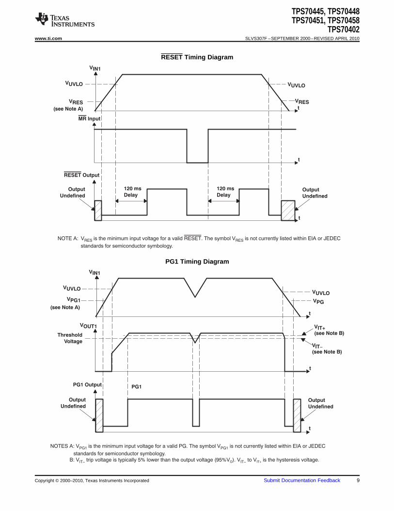
NOTE A: V is the minimum input voltage for a valid . The symbol V is not currently listed within EIA or JEDEC
standards for semiconductor symbology.
RES RESRESET
(see Note A)
VPG
t
t
t
PG1 Output
VIT+(see Note B)
VIN1
VOUT1
VPG1
V
(see Note B)
VUVLOVUVLO
PG1
Threshold
Voltage
Output
UndefinedOutput
Undefined
NOTES A: V is the minimum input voltage for a valid PG. The symbol V is not currently listed within EIA or JEDEC
standards for semiconductor symbology.
B:
PG1 PG1
V trip voltage is typically 5% lower than the output voltage (95%V ). V to V is the hysteresis voltage.IT IT- -O IT+NOTES
(see Note A)
IT-
TPS70445, TPS70448TPS70451, TPS70458
TPS70402www.ti.com SLVS307F –SEPTEMBER 2000–REVISED APRIL 2010
RESET Timing Diagram
PG1 Timing Diagram
Copyright © 2000–2010, Texas Instruments Incorporated Submit Documentation Feedback 9

t
t
PG2
Output
VIN2
t
VIT+(see Note A)
VOUT2
V
(see Note A)
Threshold
VoltageIT-
NOTE A: V trip voltage is typically 5% lower than the output voltage (95%V ). V to V is the hysteresis voltage.IT IT- -O IT+
TPS70445, TPS70448TPS70451, TPS70458TPS70402SLVS307F –SEPTEMBER 2000–REVISED APRIL 2010 www.ti.com
PG2 Timing Diagram (assuming VIN1 already powered up)
TERMINAL FUNCTIONSTERMINAL
I/O DESCRIPTIONNAME NO.
EN1 6 I Active low enable for VOUT1
EN2 7 I Active low enable for VOUT2
GND 9 — Ground
GND/HEATSI 1, 12, 13, 24 — Ground/heatsinkNK
MR 5 I Manual reset input, active low, pulled up internally
NC 4, 17, 20 — No connection
PG1 19 O Open drain output, low when VOUT1 voltage is less than 95% of the nominal regulated voltage
PG2 18 O Open drain output, low when VOUT2 voltage is less than 95% of the nominal regulated voltage
RESET 8 O Open drain output, SVS (power-on reset) signal, active low
VIN1 2, 3 I Input voltage of regulator 1
VIN2 10, 11 I Input voltage of regulator 2
VOUT1 22, 23 O Output voltage of regulator 1
VOUT2 14, 15 O Output voltage of regulator 2
VSENSE1/FB1 21 I Regulator 1 output voltage sense/regulator 1 feedback for adjustable
VSENSE2/FB2 16 I Regulator 2 output voltage sense/regulator 2 feedback for adjustable
10 Submit Documentation Feedback Copyright © 2000–2010, Texas Instruments Incorporated
TPS70445, TPS70448TPS70451, TPS70458
TPS70402www.ti.com SLVS307F –SEPTEMBER 2000–REVISED APRIL 2010
Detailed Description
The TPS704xx low dropout regulator family provides dual regulated output voltages with independent enablefunctions. These devices provide fast transient response and high accuracy with small output capacitors, whiledrawing low quiescent current. Other features are integrated SVS (power-on reset, RESET) and power good(PG1, PG2) that monitor output voltages and provide logic output to the system. These differentiated featuresprovide a complete power solution.
The TPS704xx, unlike many other LDOs, features very low quiescent current that remains virtually constant evenwith varying loads. Conventional LDO regulators use a PNP pass element, the base current of which is directlyproportional to the load current through the regulator (IB = IC/b). The TPS704xx uses a PMOS transistor to passcurrent; because the gate of the PMOS is voltage-driven, operating current is low and stable over the full loadrange.
Pin Functions
Enable (EN1, EN2)
The EN terminals are inputs that enable or shut down each respective regulator. If EN is at a voltage high signal,the respective regulator is in shutdown mode. When EN goes to voltage low, the respective regulator is enabled.
Power-Good (PG1, PG2)
The PG terminals are open drain, active high output terminals that indicate the status of each respectiveregulator. When VOUT1 reaches 95% of its regulated voltage, PG1 goes to a high impedance state. When VOUT2reaches 95% of its regulated voltage, PG2 goes to a high impedance state. Each PG goes to a low impedancestate when its respective output voltage is pulled below 95% (that is, goes to an overload condition) of itsregulated voltage. The open drain outputs of the PG terminals require a pull-up resistor.
Manual Reset Pin
MR is an active low input terminal used to trigger a reset condition. When MR is pulled to logic low, a POR(RESET) occurs. The terminal has a 6-mA pull-up current to VIN1; however, it is recommended that the pin bepulled high to VIN1 when it is not used.
Sense (VSENSE1, VSENSE2)
The sense terminals of fixed-output options must be connected to the regulator outputs, and the connectionshould be as short as possible. Internally, the sense terminal connects to high-impedance, wide-bandwidthamplifiers through a resistor-divider network and noise pickup feeds through to the regulator output. It is essentialto route the sense connection in such a way as to minimize or avoid noise pickup. Adding RC networks betweensense terminals and VOUT terminals to filter noise is not recommended because these networks can cause theregulators to oscillate.
Copyright © 2000–2010, Texas Instruments Incorporated Submit Documentation Feedback 11

TPS70445, TPS70448TPS70451, TPS70458TPS70402SLVS307F –SEPTEMBER 2000–REVISED APRIL 2010 www.ti.com
FB1 and FB2
FB1 and FB2 are input terminals used for adjustable-output devices and must be connected to the externalfeedback resistor divider. FB1 and FB2 connections should be as short as possible. It is essential to route themin such a way as to minimize or avoid noise pickup. Adding RC networks between FB terminals and VOUTterminals to filter noise is not recommended because these networks can cause the regulators to oscillate.
RESET Indicator
RESET is an active low, open drain output and requires a pullup resistor for normal operation. When pulled up,RESET goes into a high impedance state (that is, logic high) after a 120-ms delay when both of the followingconditions are met. First, VIN1 must be above the undervoltage condition. Second, the manual reset (MR) pinmust be in a high impedance state. To monitor VOUT1, the PG1 output pin can be connected to MR. To monitorVOUT2, the PG2 output pin can be connected to MR. If RESET is not used, it can be left floating.
VIN1 and VIN2
VIN1 and VIN2 are inputs to each regulator. Internal bias voltages are powered by VIN1.
VOUT1 and VOUT2
VOUT1 and VOUT2 are output terminals of each regulator.
12 Submit Documentation Feedback Copyright © 2000–2010, Texas Instruments Incorporated
1.785
1.79
1.795
1.8
1.805
0 500 1000 1500 2000
1.81
1.815
V = 2.8 V
T = 25 C
V
IN2
J
OUT2
°
I Output Current mAO - -
VO
utp
ut
Vo
ltag
eV
O-
-
3.27
3.28
3.29
3.30
3.31
0 200 400 600 800 1000
3.32
3.33
V = 4.3 V
T = 25 C
V
IN1
J
OUT1
°
I Output Current mAO - -
VO
utp
ut
Vo
ltag
eV
O-
-
TPS70445, TPS70448TPS70451, TPS70458
TPS70402www.ti.com SLVS307F –SEPTEMBER 2000–REVISED APRIL 2010
TYPICAL CHARACTERISTICS
Table of GraphsFIGURE
vs Output current Figure 1 and Figure 2VO Output voltage
vs Junction temperature Figure 3 to Figure 4
Ground current vs Junction temperature Figure 5
PSRR Power-supply rejection ratio vs Frequency Figure 6 to Figure 9
Output spectral noise density vs Frequency Figure 10 to Figure 13
ZO Output impedance vs Frequency Figure 14 to Figure 17
vs Temperature Figure 18 and Figure 19Dropout voltage
vs Input voltage Figure 20 and Figure 21
Load transient response Figure 22 and Figure 23
Line transient response (VOUT1) Figure 24
Line transient response (VOUT2) Figure 25
VO Output voltage vs Time (start-up) Figure 26 and Figure 27
Equivalent series resistance (ESR) vs Output current Figure 29 to Figure 32
TPS70451 TPS70451OUTPUT VOLTAGE OUTPUT VOLTAGE
vs vsOUTPUT CURRENT OUTPUT CURRENT
Figure 1. Figure 2.
Copyright © 2000–2010, Texas Instruments Incorporated Submit Documentation Feedback 13
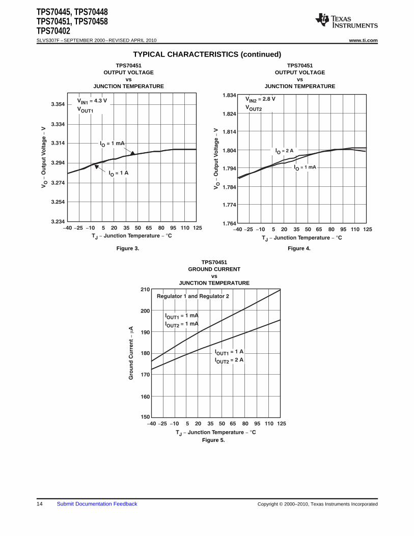
-40 -25 -10 5 20 35 50 65 80 95 110 1253.234
3.254
3.274
3.294
3.314
3.334
3.354
T Junction Temperature C- -J °
IO = 1 mA
V
VIN1
OUT1
= 4.3 V
I = 1 AO
VO
utp
ut
Vo
ltag
eV
O-
-
1.764
1.774
1.784
1.794
1.804
1.814
1.824
1.834
-40 -25 -10 5 20 35 50 65 80 95 110 125
IO = 1 mA
V
VIN2
OUT2
= 2.8 V
IO = 2 A
VO
utp
ut
Vo
ltag
eV
O-
-
T Junction Temperature C- -J °
150
160
170
180
190
200
-40 -25 -10 5 20 35 50 65 80 95 110 125
210
Regulator 1 and Regulator 2
Gro
un
d C
urr
en
tA
- m
T Junction Temperature C- -J °
I
I = 1 mAOUT1
OUT2
= 1 mA
I
I = 2 AOUT1
OUT2
= 1 A
TPS70445, TPS70448TPS70451, TPS70458TPS70402SLVS307F –SEPTEMBER 2000–REVISED APRIL 2010 www.ti.com
TYPICAL CHARACTERISTICS (continued)TPS70451 TPS70451
OUTPUT VOLTAGE OUTPUT VOLTAGEvs vs
JUNCTION TEMPERATURE JUNCTION TEMPERATURE
Figure 3. Figure 4.
TPS70451GROUND CURRENT
vsJUNCTION TEMPERATURE
Figure 5.
14 Submit Documentation Feedback Copyright © 2000–2010, Texas Instruments Incorporated
10 100 1 k 10 k 100 k 1 M
V = 4.3 V
V = 3.3 V
I = 1 A
C = 22 F
IN1
OUT1
O
O m
PS
RR
Po
wer
Su
pp
ly R
eje
cti
on
Rati
od
B-
-
f Frequency Hz- -
0
10
20
30
40
50
60
70
80
90
100
-
-
-
-
-
-
-
-
-
-10 100 1 k 10 k 100 k 1 M
V = 4.3 V
V = 3.3 V
I = 10 mA
C = 22 F
IN1
OUT1
O
O m
PS
RR
Po
wer
Su
pp
ly R
eje
cti
on
Rati
od
B-
-
f Frequency Hz- -
10
20
30
40
50
60
70
80
90
-
-
-
-
-
-
-
-
-
10 100 1 k 10 k 100 k 1 M
V = 2.8 V
V = 1.8 V
I = 10 mA
C = 47 F
IN2
OUT2
O
O m
PS
RR
Po
wer
Su
pp
ly R
eje
cti
on
Rati
od
B-
-
0
10
20
30
40
50
60
70
80
90
100
-
-
-
-
-
-
-
-
-
-
f Frequency Hz- -
10 100 1 k 10 k 100 k 1 M
PS
RR
Po
wer
Su
pp
ly R
eje
cti
on
Rati
od
B-
-
0
10
20
30
40
50
60
70
80
90
100
-
-
-
-
-
-
-
-
-
-
f Frequency Hz- -
V = 2.8 V
V = 1.8 V
I = 2 A
C = 47 F
IN2
OUT2
O
O m
TPS70445, TPS70448TPS70451, TPS70458
TPS70402www.ti.com SLVS307F –SEPTEMBER 2000–REVISED APRIL 2010
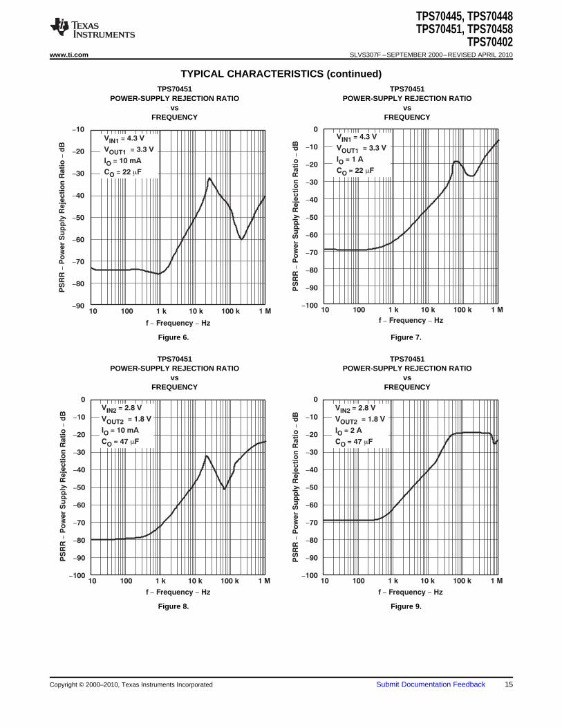
TYPICAL CHARACTERISTICS (continued)TPS70451 TPS70451
POWER-SUPPLY REJECTION RATIO POWER-SUPPLY REJECTION RATIOvs vs
FREQUENCY FREQUENCY
Figure 6. Figure 7.
TPS70451 TPS70451POWER-SUPPLY REJECTION RATIO POWER-SUPPLY REJECTION RATIO
vs vsFREQUENCY FREQUENCY
Figure 8. Figure 9.
Copyright © 2000–2010, Texas Instruments Incorporated Submit Documentation Feedback 15

0.01
0.1
1
10
100 1 k 10 k 100 k
f Frequency Hz- -
V = 4.3 V
V = 3.3 V
C = 22 F
I = 10 mA
T = 25 C
IN1
OUT1
OUT1
O
J
m
°
Ou
tpu
t S
pectr
al N
ois
e D
en
sit
y-
mV
/H
zÖ
0.01
0.1
1
10
100 1 k 10 k 100 k
V = 2.8 V
V = 1.8 V
C = 47 F
I = 10 mA
T = 25 C
IN2
OUT2
OUT2
O
J
m
°
f Frequency Hz- -
Ou
tpu
t S
pectr
al N
ois
e D
en
sit
y-
mV
/H
zÖ
0.01
0.1
1
10
100 1 k 10 k 100 k
V = 2.8 V
V = 1.8 V
C = 47 F
I = 2 A
T = 25 C
IN2
OUT2
OUT2
O
J
m
°
f Frequency Hz- -
Ou
tpu
t S
pectr
al N
ois
e D
en
sit
y-
mV
/H
zÖ
0.01
0.1
1
10
100 1 k 10 k 100 k
V = 4.3 V
V = 3.3 V
C = 22 F
I = 1 mA
T = 25 C
IN1
OUT1
OUT1
O
J
m
°
f Frequency Hz- -
Ou
tpu
t S
pectr
al N
ois
e D
en
sit
y-
mV
/H
zÖ
TPS70445, TPS70448TPS70451, TPS70458TPS70402SLVS307F –SEPTEMBER 2000–REVISED APRIL 2010 www.ti.com
TYPICAL CHARACTERISTICS (continued)OUTPUT SPECTRAL NOISE DENSITY OUTPUT SPECTRAL NOISE DENSITY
vs vsFREQUENCY FREQUENCY
Figure 10. Figure 11.
OUTPUT SPECTRAL NOISE DENSITY OUTPUT SPECTRAL NOISE DENSITYvs vs
FREQUENCY FREQUENCY
Figure 12. Figure 13.
16 Submit Documentation Feedback Copyright © 2000–2010, Texas Instruments Incorporated
0.1
0.01
10 100 1 k 10 k
1
100 k 1 M 10 M
V = 3.3 V
I = 10 mA
C = 22 F
OUT1
O
O m
ZO
utp
ut
Imp
ed
an
ce
O-
-W
f Frequency Hz- -
0.1
0.01
10 100 1 k 10 k
1
100 k 1 M 10 M
V = 3.3 V
I = 1 A
C = 22 F
OUT1
O
O m
ZO
utp
ut
Imp
ed
an
ce
O-
-W
f Frequency Hz- -
0.1
0.01
10 100 1 k 10 k
1
100 k 1 M 10 M
V = 1.8 V
I = 10 mA
C = 47 F
OUT2
O
O m
ZO
utp
ut
Imp
ed
an
ce
O-
-W
f Frequency Hz- -
0.1
0.01
10 100 1 k 10 k
1
100 k 1 M 10 M
V = 1.8 V
I = 2 A
C = 47 F
OUT2
O
O m
ZO
utp
ut
Imp
ed
an
ce
O-
-W
f Frequency Hz- -
TPS70445, TPS70448TPS70451, TPS70458
TPS70402www.ti.com SLVS307F –SEPTEMBER 2000–REVISED APRIL 2010
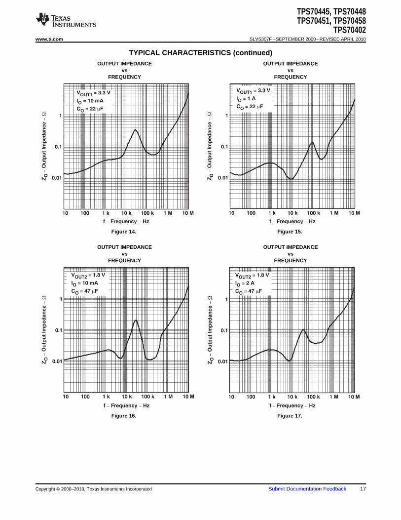
TYPICAL CHARACTERISTICS (continued)OUTPUT IMPEDANCE OUTPUT IMPEDANCE
vs vsFREQUENCY FREQUENCY
Figure 14. Figure 15.
OUTPUT IMPEDANCE OUTPUT IMPEDANCEvs vs
FREQUENCY FREQUENCY
Figure 16. Figure 17.
Copyright © 2000–2010, Texas Instruments Incorporated Submit Documentation Feedback 17

-40 -25 -10 5 20 35 50 65 80 95 110 1250
50
100
150
200
250
IO = 1 A
V
V = 3.2 VOUT1
IN1
T Temperature C- - °
Dro
po
ut
Vo
ltag
e-
mV
0
5
10
15
20
25
-40 -25 -10 5 20 35 50 65 80 95 110 125
IO = 100 mA
IO = 10 mAIO = 1 mA
V
V = 3.2 VOUT1
IN1
T Temperature C- - °
Dro
po
ut
Vo
ltag
e-
mV
0
50
100
150
200
250
2.5 3 3.5 4 4.5 5 5.5
300V
I = 1 AOUT1
O
V Input Voltage VI - -
Dro
po
ut
Vo
ltag
e-
mV T = 125 CJ °
T = 40 CJ - °
T = 25 CJ °
0
50
100
150
200
250
2.5 3 3.5 4 4.5 5 5.5
300V
I = 2 AOUT2
O
V Input Voltage VI - -
T = 125 CJ °
T = 40 CJ - °
T = 25 CJ °
Dro
po
ut
Vo
ltag
e-
mV
TPS70445, TPS70448TPS70451, TPS70458TPS70402SLVS307F –SEPTEMBER 2000–REVISED APRIL 2010 www.ti.com
TYPICAL CHARACTERISTICS (continued)TPS70451 TPS70451
DROPOUT VOLTAGE DROPOUT VOLTAGEvs vs
TEMPERATURE TEMPERATURE
Figure 18. Figure 19.
TPS70402 TPS70402DROPOUT VOLTAGE DROPOUT VOLTAGE
vs vsINPUT VOLTAGE INPUT VOLTAGE
Figure 20. Figure 21.
18 Submit Documentation Feedback Copyright © 2000–2010, Texas Instruments Incorporated

0 0.2 0.4 0.6 0.8 1 1.2 1.4 1.6 1.8 2
50
0
1
0
-50
2
V = 1.8 V
I = 2 A
C = 47 F
OUT2
O
O m
t Time ms- -D
-
-
VC
han
ge in m
VO
Ou
tpu
t V
olt
ag
eI
Ou
tpu
t C
urr
en
tA
O-
-
0 0.2 0.4 0.6 0.8 1 1.2 1.4 1.6 1.8 2
0
0.5
0
-50
-100
1
50
V = 4.3 V
V = 3.3 V
C = 22 F
IN1
OUT1
O m
D-
-
VC
han
ge in m
VO
Ou
tpu
t V
olt
ag
eI
Ou
tpu
t C
urr
en
tA
O-
-
t Time ms- -
0 20 40 60 80 100 120 140 160 180 20
100
2.8
0
100
3.8
200
V = 1.8 V
I = 2 A
C = 47 F
OUT2
O
O m
t Time s- - m
D-
-
VC
han
ge in m
VO
Ou
tpu
t V
olt
ag
eV
Inp
ut
Vo
ltag
eV
I-
-
0 20 40 60 80 100 120 140 160 180 200
50
4.3
0
50
5.3
100
V = 3.3 V
I = 1 A
C = 22 F
OUT1
O
O m
t Time s- - m
D-
-
VC
han
ge in m
VO
Ou
tpu
t V
olt
ag
eV
Inp
ut
Vo
ltag
eV
I-
-
TPS70445, TPS70448TPS70451, TPS70458
TPS70402www.ti.com SLVS307F –SEPTEMBER 2000–REVISED APRIL 2010
TYPICAL CHARACTERISTICS (continued)LOAD TRANSIENT RESPONSE LOAD TRANSIENT RESPONSE
Figure 22. Figure 23.
LINE TRANSIENT RESPONSE LINE TRANSIENT RESPONSE
Figure 24. Figure 25.
Copyright © 2000–2010, Texas Instruments Incorporated Submit Documentation Feedback 19

0 2
3
1
0
0
5
0.2 1.81.61.41.210.4 0.6 0.8
2
4
V = 3.3 V
I = 1 A
C = 22 F
V = 4.3 V
= High
OUT1
O
O
IN1
m
EN2
En
ab
le V
olt
ag
e-
VV
Ou
tpu
t V
olt
ag
eV
O-
-
t Time ms- -
0 2
2
1
0
0
5
0.2 1.81.61.41.210.4 0.6 0.8
V = 1.8 V
I = 2 A
C = 47 F
V = 2.8 V
= High
OUT2
O
O
IN2
m
EN1
t Time ms- -
En
ab
le V
olt
ag
e-
VV
Ou
tpu
t V
olt
ag
eV
O-
-
IN
EN
OUT
GND
ESR
VIN
COUT
To Load
RL
+
TPS70445, TPS70448TPS70451, TPS70458TPS70402SLVS307F –SEPTEMBER 2000–REVISED APRIL 2010 www.ti.com
TYPICAL CHARACTERISTICS (continued)OUTPUT VOLTAGE AND ENABLE VOLTAGE OUTPUT VOLTAGE AND ENABLE VOLTAGE
vs vsTIME (START-UP) TIME (START-UP)
Figure 26. Figure 27.
Figure 28. Test Circuit for Typical Regions of Stability
20 Submit Documentation Feedback Copyright © 2000–2010, Texas Instruments Incorporated

0.1
0.01
10
1
0 0.2
REGION OF INSTABILITY
0.1 0.3 0.4 0.5 0.6 0.7 0.8 0.9 1
V = 3.3 VOUT1
C = 220 FmO
15 mW
I Output Current- -O A
ES
RE
qu
ivale
nt
Seri
es R
esis
tan
ce
-W
-
0.1
0.01
10
1
0 0.2
REGION OF INSTABILITY
0.1 0.3 0.4 0.5 0.6 0.7 0.8 0.9 1
V = 3.3 VOUT1
C = 22 FmO
ES
RE
qu
ivale
nt
Seri
es R
esis
tan
ce
-W
-
50 mW
I Output Current- -O A
0.1
0.01
10
1
0 0.20.1 0.3 0.4 0.5 0.6 0.7 0.8 0.9 1
REGION OF INSTABILITY
V = 1.8 VOUT2
C = 680 FmO
15 mW
I Output Current- -O A
ES
RE
qu
ivale
nt
Seri
es R
esis
tan
ce
-W
-
0.1
0.01
10
1
0 0.2
REGION OF INSTABILITY
0.1 0.3 0.4 0.5 0.6 0.7 0.8 0.9 1
V = 1.8 VOUT2
C = 47 FmO
50 mW
I Output Current- -O A
ES
RE
qu
ivale
nt
Seri
es R
esis
tan
ce
-W
-
TPS70445, TPS70448TPS70451, TPS70458
TPS70402www.ti.com SLVS307F –SEPTEMBER 2000–REVISED APRIL 2010
TYPICAL CHARACTERISTICS (continued)TYPICAL REGION OF STABILITY TYPICAL REGION OF STABILITY
EQUIVALENT SERIES RESISTANCE(1) EQUIVALENT SERIES RESISTANCE(1)
vs vsOUTPUT CURRENT OUTPUT CURRENT
Figure 29. Figure 30.
TYPICAL REGION OF STABILITY TYPICAL REGION OF STABILITYEQUIVALENT SERIES RESISTANCE(1) EQUIVALENT SERIES RESISTANCE(1)
vs vsOUTPUT CURRENT OUTPUT CURRENT
Figure 31. Figure 32.
(1) Equivalent series resistance (ESR) refers to the total series resistance, including the ESR of the capacitor, anyseries resistance added externally, and PWB trace resistance to CO.
Copyright © 2000–2010, Texas Instruments Incorporated Submit Documentation Feedback 21

DIE
Side View (a)
End View (b)
DIE
Thermal
Pad
Bottom View (c)
TPS70445, TPS70448TPS70451, TPS70458TPS70402SLVS307F –SEPTEMBER 2000–REVISED APRIL 2010 www.ti.com
THERMAL INFORMATION
Thermally-Enhanced TSSOP-24 (PWP— PowerPAD™)
The thermally-enhanced PWP package is based on the 24-pin TSSOP, but includes a thermal pad [seeFigure 33(c)] to provide an effective thermal contact between the IC and the printed wiring board (PWB).
Traditionally, surface mount and power have been mutually exclusive terms. A variety of scaled-downTO220-type packages have leads formed as gull wings to make them applicable for surface-mount applications.These packages, however, suffer from several shortcomings: they do not address the very low profilerequirements (<2 mm) of many of today’s advanced systems, and they do not offer a pin-count high enough toaccommodate increasing integration. On the other hand, traditional low-power surface-mount packages requirepower-dissipation derating that severely limits the usable range of many high-performance analog circuits.
The PWP package (thermally-enhanced TSSOP) combines fine-pitch surface-mount technology with thermalperformance comparable to much larger power packages.
The PWP package is designed to optimize the heat transfer to the PWB. Because of the very small size andlimited mass of a TSSOP package, thermal enhancement is achieved by improving the thermal conduction pathsthat remove heat from the component. The thermal pad is formed using a lead-frame design (patent pending)and manufacturing technique to provide the user with direct connection to the heat-generating IC. When this padis soldered or otherwise coupled to an external heat dissipator, high power dissipation in the ultrathin, fine-pitch,surface-mount package can be reliably achieved.
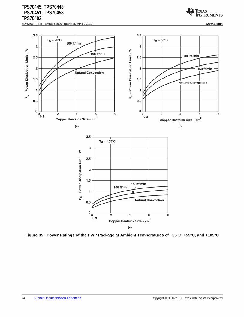
Figure 33. Views of Thermally-Enhanced PWP Package
Because the conduction path has been enhanced, power-dissipation capability is determined by the thermalconsiderations in the PWB design. For example, simply adding a localized copper plane (heat-sink surface),which is coupled to the thermal pad, enables the PWP package to dissipate 2.5 W in free air (referenceFigure 35(a), 8 cm2 of copper heat sink and natural convection). Increasing the heat-sink size increases thepower dissipation range for the component. The power dissipation limit can be further improved by adding airflowto a PWB/IC assembly (see Figure 34 and Figure 35). The line drawn at 0.3 cm2 in Figure 34 and Figure 35indicates performance at the minimum recommended heat-sink size, illustrated in Figure 36.
22 Submit Documentation Feedback Copyright © 2000–2010, Texas Instruments Incorporated

100
75
50
25
0 2 3 5
125
150
7 81 4 60.3
Natural Convection
50 ft/min
250 ft/min
300 ft/min
100 ft/min
150 ft/min
200 ft/min
Copper Heatsink Area - cm2
RT
herm
al R
esis
tan
ce
-C
/WqJA
-°
TPS70445, TPS70448TPS70451, TPS70458
TPS70402www.ti.com SLVS307F –SEPTEMBER 2000–REVISED APRIL 2010
The thermal pad is directly connected to the substrate of the IC, which for the TPS704xx series is a secondaryelectrical connection to device ground. The heat-sink surface that is added to the PWP can be a ground plane orleft electrically isolated. In TO220-type surface-mount packages, the thermal connection is also the primaryelectrical connection for a given terminal which is not always ground. The PWP package provides up to 24independent leads that can be used as inputs and outputs (Note: leads 1, 12, 13, and 24 are internallyconnected to the thermal pad and the IC substrate).
THERMAL RESISTANCEvs COPPER HEATSINK AREA
Figure 34.
Copyright © 2000–2010, Texas Instruments Incorporated Submit Documentation Feedback 23
1
0.5
3
00 2 4 6
2
1.5
2.5
3.5
80.3
300 ft/min
150 ft/min
Natural Convection
TA = 55°C
(b)
1
0.5
3
00 2 4 6
2
1.5
2.5
3.5
80.3
300 ft/min150 ft/min
Natural Convection
TA = 105°C
(c)
1
0.5
3
00 2 4 6
2
1.5
2.5
3.5
80.3
300 ft/min
150 ft/min
Natural Convection
TA = 25°C
(a)
Copper Heatsink Size - cm2
PP
ow
er
Dis
sip
ati
on
Lim
it-
WD
-
Copper Heatsink Size - cm2
PP
ow
er
Dis
sip
ati
on
Lim
it-
WD
-
Copper Heatsink Size - cm2
PP
ow
er
Dis
sip
ati
on
Lim
it-
WD
-
TPS70445, TPS70448TPS70451, TPS70458TPS70402SLVS307F –SEPTEMBER 2000–REVISED APRIL 2010 www.ti.com
Figure 35. Power Ratings of the PWP Package at Ambient Temperatures of +25°C, +55°C, and +105°C
24 Submit Documentation Feedback Copyright © 2000–2010, Texas Instruments Incorporated

Board thickness 62 mils
Board size
Board material FR4
Copper trace/heat sink 1 oz
Exposed pad mounting 63/67 tin/lead solder
Heatsink Area
1 oz Copper
3.2 in 3.2 in´
P =D(max)
T T-Jmax A
RqJA(system)
P =D(total) V V-IN1 OUT1( ( V V-IN2 OUT2( (´ I + V ´ +OUT1 IN1
I
2
Q I
2
Q´ ´I + VOUT2 IN2
P =D(total) V V-IN1 OUT1( ( V V-IN2 OUT2( (´ I +OUT1 ´ IOUT2
P =D(max)
T T-Jmax A
RqJA(system)
=+125 C 55 C-° °
+50°C/W= 1.4 W
P =D(total) V V-IN1 OUT1( ( V V-IN2 OUT2( (´ I +OUT1 ´ IOUT2
= (5.0 3.3) 0.5 + (2.8 1.8) 0.8 = 1.25 W- -´ ´
TPS70445, TPS70448TPS70451, TPS70458
TPS70402www.ti.com SLVS307F –SEPTEMBER 2000–REVISED APRIL 2010
Figure 36 is an example of a thermally-enhanced PWB layout for use with the new PWP package. This boardconfiguration was used in the thermal experiments that generated the power ratings shown in Figure 34 andFigure 35. As discussed earlier, copper has been added on the PWB to conduct heat away from the device. RqJAfor this assembly is illustrated in Figure 34 as a function of heat-sink area. A family of curves is included toillustrate the effect of airflow introduced into the system.
Figure 36. PWB Layout (Including Copper Heatsink Area) for Thermally-Enhanced PWP Package
From Figure 34, RqJA for a PWB assembly can be determined and used to calculate the maximumpower-dissipation limit for the component/PWB assembly, with the equation:
where:• TJmax is the maximum specified junction temperature (+150°C absolute maximum limit, +125°C recommended
operating limit) and TA is the ambient temperature. (1)
PD(max) should then be applied to the internal power dissipated by the TPS704xx regulator. The equation forcalculating total internal power dissipation of the TPS704xx is:
(2)
Since the quiescent current of the TPS704xx is very low, the second term is negligible, further simplifying theequation to:
(3)
For the case where TA = +55°C, airflow = 200 ft/min, copper heat-sink area = 4 cm2, the maximumpower-dissipation limit can be calculated. First, from Figure 34, we find the system RqJA is +50°C/W; therefore,the maximum power-dissipation limit is:
(4)
If the system implements a TPS704xx regulator, where VIN1 = 5.0V, VIN2 = 2.8 V, IOUT1 = 500 mA, and IOUT2 =800 mA, the internal power dissipation is:
(5)
Copyright © 2000–2010, Texas Instruments Incorporated Submit Documentation Feedback 25

Location of Exposed
Thermal Pad on
PWP Package
Minimum Recommended
Heatsink Area
TPS70445, TPS70448TPS70451, TPS70458TPS70402SLVS307F –SEPTEMBER 2000–REVISED APRIL 2010 www.ti.com
Comparing PD(total) with PD(max) reveals that the power dissipation in this example does not exceed the calculatedlimit. When it does, one of two corrective actions should be made: raising the power-dissipation limit byincreasing the airflow or the heat-sink area, or lowering the internal power dissipation of the regulator by reducingthe input voltage or the load current. In either case, the above calculations should be repeated with the newsystem parameters. This parameter is measured with the recommended copper heat sink pattern on a 4-layerPWB, 2 oz. copper traces on 4-in × 4-in ground layer. Simultaneous and continuous operation of both regulatoroutputs at full load may exceed the power dissipation rating of the PWP package.
Mounting Information
The primary requirement is to complete the thermal contact between the thermal pad and the PWB metal. Thethermal pad is a solderable surface and is fully intended to be soldered at the time the component is mounted.Although voiding in the thermal-pad solder-connection is not desirable, up to 50% voiding is acceptable. The dataincluded in Figure 34 and Figure 36 are for soldered connections with voiding between 20% and 50%. Thethermal analysis shows no significant difference resulting from the variation in voiding percentage.
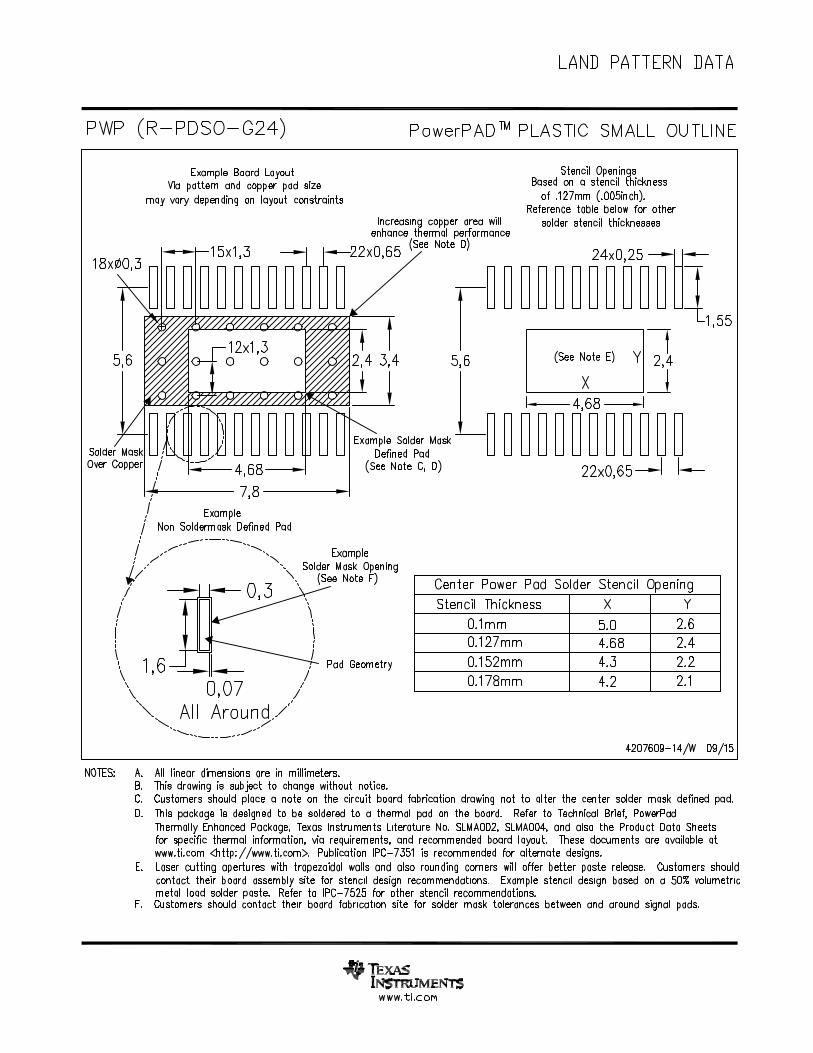
Figure 37 shows the solder-mask land pattern for the PWP package. The minimum recommended heat-sink areais also illustrated. This is simply a copper plane under the body extent of the package, including metal routedunder terminals 1, 12, 13, and 24.
Figure 37. PWP Package Land Pattern
26 Submit Documentation Feedback Copyright © 2000–2010, Texas Instruments Incorporated
>2 V
<0.7 V
>2 V
<0.7 V
TPS704xxPWP
(Fixed Output Option)
0.22 Fm
0.22 Fm
47 Fm
22 Fm250 kW
250 kW
RESETRESET
VINVIN1
VIN2
VOUT1
VSENSE1
PG1
MRMR
VOUT1
EN1
EN2
EN1
EN2
VSENSE2
VOUT2
PG2PG2
VOUT2
95%
95%
PG2
PG1
NOTES: A. t : Time at which V is greater than V and is logic high.
B. The timing diagram is not drawn to scale.
1 IN UVLO MR
120 mst1
EN2
EN1
VOUT2
VOUT1
MR
MR(PG2 tied to )
RESET
TPS70445, TPS70448TPS70451, TPS70458
TPS70402www.ti.com SLVS307F –SEPTEMBER 2000–REVISED APRIL 2010
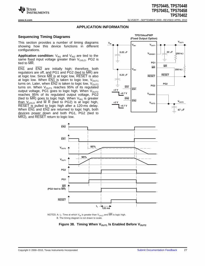
APPLICATION INFORMATION
Sequencing Timing Diagrams
This section provides a number of timing diagramsshowing how this device functions in differentconfigurations.
Application condition: VIN1 and VIN2 are tied to thesame fixed input voltage greater than VUVLO. PG2 istied to MR.
EN1 and EN2 are initially high; therefore, bothregulators are off, and PG1 and PG2 (tied to MR) areat logic low. Since MR is at logic low, RESET is alsoat logic low. When EN1 is taken to logic low, VOUT1turns on. Later, when EN2 is taken to logic low, VOUT2turns on. When VOUT1 reaches 95% of its regulatedoutput voltage, PG1 goes to logic high. When VOUT2reaches 95% of its regulated output voltage, PG2(tied to MR) goes to logic high. When VIN1 is greaterthan VUVLO and M R (tied to PG2) is at logic high,RESET is pulled to logic high after a 120-ms delay.When EN1 and EN2 are returned to logic high, bothdevices power down and both PG1, PG2 (tied toMR2), and RESET return to logic low.
Figure 38. Timing When VOUT1 Is Enabled Before VOUT2
Copyright © 2000–2010, Texas Instruments Incorporated Submit Documentation Feedback 27

2 V
0.7 V
TPS704xxPWP
(Fixed Output Option)
22 Fm
0.22 Fm
0.22 Fm
250 kW
250 kW
250 kW
47 Fm
EN1
EN2
>2 V
<0.7 V
>2 V
<0.7 V
EN2
EN1
VIN2
VIN1
VIN
VOUT2
VSENSE2
MR
PG2
RESET
VSENSE1
VOUT1
MR
RESET
PG2
VOUT2
VOUT1
95%
95%
EN2
EN1
VOUT1
VOUT2
PG2
PG1
MR
RESET
NOTES: A. t : Time at which V is greater than V and is logic high.
B. The timing diagram is not drawn to scale.
1 IN UVLO MR
120 mst1
TPS70445, TPS70448TPS70451, TPS70458TPS70402SLVS307F –SEPTEMBER 2000–REVISED APRIL 2010 www.ti.com
Application condition: VIN1 and VIN2 are tied to thesame fixed input voltage greater than VUVLO. MR isinitially logic high but is eventually toggled.
EN1 and EN2 are initially high; therefore, bothregulators are off, and PG1 and PG2 are at logic low.Since VIN1 is greater than VUVLO and MR is at logichigh, RESET is also at logic high. When EN2 is takento logic low, VOUT2 turns on. Later, when EN1 is takento logic low, VOUT1 turns on. When VOUT2 reaches95% of its regulated output voltage, PG2 goes tologic high. When VOUT1 reaches 95% of its regulatedoutput voltage, PG1 goes to logic high. When MR istaken to logic low, RESET is taken low. When MRreturns to logic high, RESET returns to logic highafter a 120-ms delay.
Figure 39. Timing When MR is Toggled
28 Submit Documentation Feedback Copyright © 2000–2010, Texas Instruments Incorporated
TPS704xxPWP
(Fixed Output Option)
0.22 Fm 22 Fm
0.22 Fm
250 kW
250 kW
47 Fm
>2 V
<0.7 V
>2 V
<0.7 V
EN1
EN2
EN1
EN2
VIN1
VIN2
VIN
RESET
VOUT1
VSENSE1
PG1
MR
VSENSE2
VOUT2
PG2
VOUT2
RESET
PG2
VOUT1
95%
95%
EN2
EN1
VOUT1
VOUT2
PG2
PG1
MR
MR(PG1 tied to )
RESET
FAULT ON VOUT1
NOTES: A. t : Time at which V is greater than V and is logic high.
B. The timing diagram is not drawn to scale.
1 IN UVLO MR
120 mst1
TPS70445, TPS70448TPS70451, TPS70458
TPS70402www.ti.com SLVS307F –SEPTEMBER 2000–REVISED APRIL 2010
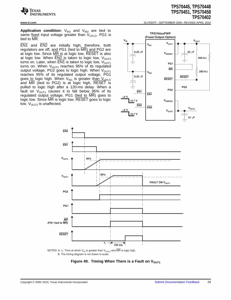
Application condition: VIN1 and VIN2 are tied tosame fixed input voltage greater than VUVLO. PG1 istied to MR.
EN1 and EN2 are initially high; therefore, bothregulators are off, and PG1 (tied to MR) and PG2 areat logic low. Since MR is at logic low, RESET is alsoat logic low. When EN2 is taken to logic low, VOUT2turns on. Later, when EN1 is taken to logic low, VOUT1turns on. When VOUT2 reaches 95% of its regulatedoutput voltage, PG2 goes to logic high. When VOUT1reaches 95% of its regulated output voltage, PG1goes to logic high. When VIN1 is greater than VUVLOand MR (tied to PG2) is at logic high, RESET ispulled to logic high after a 120-ms delay. When afault on VOUT1 causes it to fall below 95% of itsregulated output voltage, PG1 (tied to MR) goes tologic low. Since MR is logic low, RESET goes to logiclow. VOUT2 is unaffected.
Figure 40. Timing When There is a Fault on VOUT1
Copyright © 2000–2010, Texas Instruments Incorporated Submit Documentation Feedback 29
TPS70445, TPS70448TPS70451, TPS70458TPS70402SLVS307F –SEPTEMBER 2000–REVISED APRIL 2010 www.ti.com
APPLICATION INFORMATION
Input Capacitor
For a typical application, a ceramic input bypass capacitor (0.22 mF to 1 mF) is recommended. This capacitorshould be as close to the input pins as possible. Due to the impedance of the input supply, large transientcurrents cause the input voltage to droop. If this droop causes the input voltage to drop below the UVLOthreshold, the device turns off. Therefore, it is recommended to place a larger capacitor in parallel with theceramic bypass capacitor at the regulator input. The size of this capacitor depends on the output current, theresponse time of the main power supply, and the main power supply distance to the regulator. At a minimum, thecapacitor should be sized to ensure that the input voltage does not drop below the minimum UVLO thresholdvoltage during normal operating conditions.
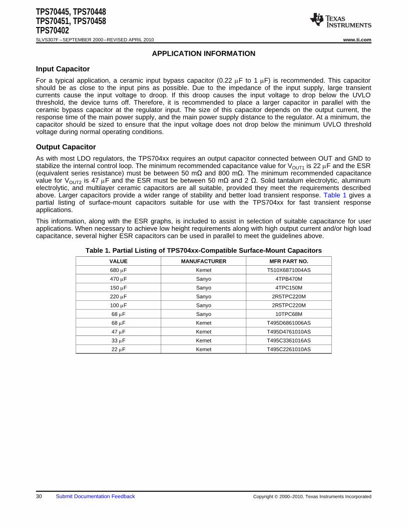
Output Capacitor
As with most LDO regulators, the TPS704xx requires an output capacitor connected between OUT and GND tostabilize the internal control loop. The minimum recommended capacitance value for VOUT1 is 22 mF and the ESR(equivalent series resistance) must be between 50 mΩ and 800 mΩ. The minimum recommended capacitancevalue for VOUT2 is 47 mF and the ESR must be between 50 mΩ and 2 Ω. Solid tantalum electrolytic, aluminumelectrolytic, and multilayer ceramic capacitors are all suitable, provided they meet the requirements describedabove. Larger capacitors provide a wider range of stability and better load transient response. Table 1 gives apartial listing of surface-mount capacitors suitable for use with the TPS704xx for fast transient responseapplications.
This information, along with the ESR graphs, is included to assist in selection of suitable capacitance for userapplications. When necessary to achieve low height requirements along with high output current and/or high loadcapacitance, several higher ESR capacitors can be used in parallel to meet the guidelines above.
Table 1. Partial Listing of TPS704xx-Compatible Surface-Mount Capacitors
VALUE MANUFACTURER MFR PART NO.
680 mF Kemet T510X6871004AS
470 mF Sanyo 4TPB470M
150 mF Sanyo 4TPC150M
220 mF Sanyo 2R5TPC220M
100 mF Sanyo 2R5TPC220M
68 mF Sanyo 10TPC68M
68 mF Kemet T495D6861006AS
47 mF Kemet T495D4761010AS
33 mF Kemet T495C3361016AS
22 mF Kemet T495C2261010AS
30 Submit Documentation Feedback Copyright © 2000–2010, Texas Instruments Incorporated

R1 =V
V
OUT
REF
- 1 ´ R2( (
OUTPUT VOLTAGE
PROGRAMMING GUIDE
VO
VI
OUT
FB
R1
R2GND
EN
IN
<0.7 V
>2.0 V
TPS70402
0.1 mF
+
OUTPUT
VOLTAGER1 R2
2.5 V
3.3 V
3.6 V
UNIT
31.6
51.1
59.0
30.1
30.1
30.1
kW
kW
kW
TPS70445, TPS70448TPS70451, TPS70458
TPS70402www.ti.com SLVS307F –SEPTEMBER 2000–REVISED APRIL 2010
Programming the TPS70402 Adjustable LDO Regulator
The output voltage of the TPS70402 adjustable regulators is programmed using external resistor dividers asshown in Figure 41.
Resistors R1 and R2 should be chosen for approximately a 50-mA divider current. Lower value resistors can beused, but offer no inherent advantage and waste more power. Higher values should be avoided as leakagecurrents at the sense terminal increase the output voltage error. The recommended design procedure is tochoose R2 = 30.1 kΩ to set the divider current at approximately 50 mA, and then calculate R1 using Equation 6:
(6)
where:• VREF = 1.224 V typ (the internal reference voltage)
Figure 41. TPS70402 Adjustable LDO Regulator Programming
Regulator Protection
Both TPS704xx PMOS-pass transistors have built-in back diodes that conduct reverse currents when the inputvoltage drops below the output voltage (for example, during power-down). Current is conducted from the outputto the input and is not internally limited. When extended reverse voltage is anticipated, external limiting may beappropriate.
The TPS704xx also features internal current limiting and thermal protection. During normal operation, theTPS704xx regulator 1 limits output current to approximately 1.75 A (typ) and regulator 2 limits output current toapproximately 3.8 A (typ). When current limiting engages, the output voltage scales back linearly until theovercurrent condition ends. While current limiting is designed to prevent gross device failure, care should betaken not to exceed the power dissipation ratings of the package. If the temperature of the device exceeds+150°C (typ), thermal-protection circuitry shuts it down. Once the device has cooled below +130°C (typ),regulator operation resumes.
Copyright © 2000–2010, Texas Instruments Incorporated Submit Documentation Feedback 31

TPS70445, TPS70448TPS70451, TPS70458TPS70402SLVS307F –SEPTEMBER 2000–REVISED APRIL 2010 www.ti.com
REVISION HISTORY
NOTE: Page numbers for previous revisions may differ from page numbers in the current version.
Changes from Revision E (February 2010) to Revision F Page
• Changed Tube transport media, quatity values from 70 to 60 in Ordering Information table .............................................. 3
Changes from Revision D (December, 2007) to Revision E Page
• Corrected pin description for pin 21 in pinout drawing ......................................................................................................... 1
• Updated Dissipation Ratings table values ............................................................................................................................ 4
• Deleted falling edge delay specification ................................................................................................................................ 6
• Updated Fixed Voltage Version block diagram .................................................................................................................... 7
• Updated Adjustable Voltage Version block diagram ............................................................................................................ 8
32 Submit Documentation Feedback Copyright © 2000–2010, Texas Instruments Incorporated

PACKAGE OPTION ADDENDUM
www.ti.com 10-Jun-2014
Addendum-Page 1
PACKAGING INFORMATION
Orderable Device Status(1)
Package Type PackageDrawing
Pins PackageQty
Eco Plan(2)
Lead/Ball Finish(6)
MSL Peak Temp(3)
Op Temp (°C) Device Marking(4/5)
Samples
TPS70402PWP ACTIVE HTSSOP PWP 24 60 Green (RoHS& no Sb/Br)
CU NIPDAU Level-2-260C-1 YEAR -40 to 125 PT70402
TPS70402PWPG4 ACTIVE HTSSOP PWP 24 60 Green (RoHS& no Sb/Br)
CU NIPDAU Level-2-260C-1 YEAR -40 to 125 PT70402
TPS70402PWPR ACTIVE HTSSOP PWP 24 2000 Green (RoHS& no Sb/Br)
CU NIPDAU Level-2-260C-1 YEAR -40 to 125 PT70402
TPS70402PWPRG4 ACTIVE HTSSOP PWP 24 2000 Green (RoHS& no Sb/Br)
CU NIPDAU Level-2-260C-1 YEAR -40 to 125 PT70402
TPS70445PWP ACTIVE HTSSOP PWP 24 60 Green (RoHS& no Sb/Br)
CU NIPDAU Level-2-260C-1 YEAR -40 to 125 PT70445
TPS70445PWPG4 ACTIVE HTSSOP PWP 24 60 Green (RoHS& no Sb/Br)
CU NIPDAU Level-2-260C-1 YEAR -40 to 125 PT70445
TPS70445PWPR ACTIVE HTSSOP PWP 24 2000 Green (RoHS& no Sb/Br)
CU NIPDAU Level-2-260C-1 YEAR -40 to 125 PT70445
TPS70448PWP ACTIVE HTSSOP PWP 24 60 Green (RoHS& no Sb/Br)
CU NIPDAU Level-2-260C-1 YEAR -40 to 125 PT70448
TPS70448PWPG4 ACTIVE HTSSOP PWP 24 60 Green (RoHS& no Sb/Br)
CU NIPDAU Level-2-260C-1 YEAR -40 to 125 PT70448
TPS70448PWPR ACTIVE HTSSOP PWP 24 2000 Green (RoHS& no Sb/Br)
CU NIPDAU Level-2-260C-1 YEAR -40 to 125 PT70448
TPS70451PWP ACTIVE HTSSOP PWP 24 60 Green (RoHS& no Sb/Br)
CU NIPDAU Level-2-260C-1 YEAR -40 to 125 PT70451
TPS70451PWPG4 ACTIVE HTSSOP PWP 24 60 Green (RoHS& no Sb/Br)
CU NIPDAU Level-2-260C-1 YEAR -40 to 125 PT70451
TPS70451PWPR ACTIVE HTSSOP PWP 24 2000 Green (RoHS& no Sb/Br)
CU NIPDAU Level-2-260C-1 YEAR -40 to 125 PT70451
TPS70451PWPRG4 ACTIVE HTSSOP PWP 24 2000 Green (RoHS& no Sb/Br)
CU NIPDAU Level-2-260C-1 YEAR -40 to 125 PT70451
TPS70458PWP ACTIVE HTSSOP PWP 24 60 Green (RoHS& no Sb/Br)
CU NIPDAU Level-2-260C-1 YEAR -40 to 125 PT70458
TPS70458PWPG4 ACTIVE HTSSOP PWP 24 60 Green (RoHS& no Sb/Br)
CU NIPDAU Level-2-260C-1 YEAR -40 to 125 PT70458
TPS70458PWPR ACTIVE HTSSOP PWP 24 2000 Green (RoHS& no Sb/Br)
CU NIPDAU Level-2-260C-1 YEAR -40 to 125 PT70458

PACKAGE OPTION ADDENDUM
www.ti.com 10-Jun-2014
Addendum-Page 2
Orderable Device Status(1)
Package Type PackageDrawing
Pins PackageQty
Eco Plan(2)
Lead/Ball Finish(6)
MSL Peak Temp(3)
Op Temp (°C) Device Marking(4/5)
Samples
TPS70458PWPRG4 ACTIVE HTSSOP PWP 24 2000 Green (RoHS& no Sb/Br)
CU NIPDAU Level-2-260C-1 YEAR -40 to 125 PT70458
(1) The marketing status values are defined as follows:ACTIVE: Product device recommended for new designs.LIFEBUY: TI has announced that the device will be discontinued, and a lifetime-buy period is in effect.NRND: Not recommended for new designs. Device is in production to support existing customers, but TI does not recommend using this part in a new design.PREVIEW: Device has been announced but is not in production. Samples may or may not be available.OBSOLETE: TI has discontinued the production of the device.
(2) Eco Plan - The planned eco-friendly classification: Pb-Free (RoHS), Pb-Free (RoHS Exempt), or Green (RoHS & no Sb/Br) - please check http://www.ti.com/productcontent for the latest availabilityinformation and additional product content details.TBD: The Pb-Free/Green conversion plan has not been defined.Pb-Free (RoHS): TI's terms "Lead-Free" or "Pb-Free" mean semiconductor products that are compatible with the current RoHS requirements for all 6 substances, including the requirement thatlead not exceed 0.1% by weight in homogeneous materials. Where designed to be soldered at high temperatures, TI Pb-Free products are suitable for use in specified lead-free processes.Pb-Free (RoHS Exempt): This component has a RoHS exemption for either 1) lead-based flip-chip solder bumps used between the die and package, or 2) lead-based die adhesive used betweenthe die and leadframe. The component is otherwise considered Pb-Free (RoHS compatible) as defined above.Green (RoHS & no Sb/Br): TI defines "Green" to mean Pb-Free (RoHS compatible), and free of Bromine (Br) and Antimony (Sb) based flame retardants (Br or Sb do not exceed 0.1% by weightin homogeneous material)
(3) MSL, Peak Temp. - The Moisture Sensitivity Level rating according to the JEDEC industry standard classifications, and peak solder temperature.
(4) There may be additional marking, which relates to the logo, the lot trace code information, or the environmental category on the device.
(5) Multiple Device Markings will be inside parentheses. Only one Device Marking contained in parentheses and separated by a "~" will appear on a device. If a line is indented then it is a continuationof the previous line and the two combined represent the entire Device Marking for that device.
(6) Lead/Ball Finish - Orderable Devices may have multiple material finish options. Finish options are separated by a vertical ruled line. Lead/Ball Finish values may wrap to two lines if the finishvalue exceeds the maximum column width.
Important Information and Disclaimer:The information provided on this page represents TI's knowledge and belief as of the date that it is provided. TI bases its knowledge and belief on informationprovided by third parties, and makes no representation or warranty as to the accuracy of such information. Efforts are underway to better integrate information from third parties. TI has taken andcontinues to take reasonable steps to provide representative and accurate information but may not have conducted destructive testing or chemical analysis on incoming materials and chemicals.TI and TI suppliers consider certain information to be proprietary, and thus CAS numbers and other limited information may not be available for release.
In no event shall TI's liability arising out of such information exceed the total purchase price of the TI part(s) at issue in this document sold by TI to Customer on an annual basis.

TAPE AND REEL INFORMATION
*All dimensions are nominal
Device PackageType
PackageDrawing
Pins SPQ ReelDiameter
(mm)
ReelWidth
W1 (mm)
A0(mm)
B0(mm)
K0(mm)
P1(mm)
W(mm)
Pin1Quadrant
TPS70402PWPR HTSSOP PWP 24 2000 330.0 16.4 6.95 8.3 1.6 8.0 16.0 Q1
TPS70445PWPR HTSSOP PWP 24 2000 330.0 16.4 6.95 8.3 1.6 8.0 16.0 Q1
TPS70448PWPR HTSSOP PWP 24 2000 330.0 16.4 6.95 8.3 1.6 8.0 16.0 Q1
TPS70451PWPR HTSSOP PWP 24 2000 330.0 16.4 6.95 8.3 1.6 8.0 16.0 Q1
TPS70458PWPR HTSSOP PWP 24 2000 330.0 16.4 6.95 8.3 1.6 8.0 16.0 Q1
PACKAGE MATERIALS INFORMATION
www.ti.com 14-Jul-2012
Pack Materials-Page 1

*All dimensions are nominal
Device Package Type Package Drawing Pins SPQ Length (mm) Width (mm) Height (mm)
TPS70402PWPR HTSSOP PWP 24 2000 367.0 367.0 38.0
TPS70445PWPR HTSSOP PWP 24 2000 367.0 367.0 38.0
TPS70448PWPR HTSSOP PWP 24 2000 367.0 367.0 38.0
TPS70451PWPR HTSSOP PWP 24 2000 367.0 367.0 38.0
TPS70458PWPR HTSSOP PWP 24 2000 367.0 367.0 38.0
PACKAGE MATERIALS INFORMATION
www.ti.com 14-Jul-2012
Pack Materials-Page 2
IMPORTANT NOTICE
Texas Instruments Incorporated and its subsidiaries (TI) reserve the right to make corrections, enhancements, improvements and otherchanges to its semiconductor products and services per JESD46, latest issue, and to discontinue any product or service per JESD48, latestissue. Buyers should obtain the latest relevant information before placing orders and should verify that such information is current andcomplete. All semiconductor products (also referred to herein as “components”) are sold subject to TI’s terms and conditions of salesupplied at the time of order acknowledgment.TI warrants performance of its components to the specifications applicable at the time of sale, in accordance with the warranty in TI’s termsand conditions of sale of semiconductor products. Testing and other quality control techniques are used to the extent TI deems necessaryto support this warranty. Except where mandated by applicable law, testing of all parameters of each component is not necessarilyperformed.TI assumes no liability for applications assistance or the design of Buyers’ products. Buyers are responsible for their products andapplications using TI components. To minimize the risks associated with Buyers’ products and applications, Buyers should provideadequate design and operating safeguards.TI does not warrant or represent that any license, either express or implied, is granted under any patent right, copyright, mask work right, orother intellectual property right relating to any combination, machine, or process in which TI components or services are used. Informationpublished by TI regarding third-party products or services does not constitute a license to use such products or services or a warranty orendorsement thereof. Use of such information may require a license from a third party under the patents or other intellectual property of thethird party, or a license from TI under the patents or other intellectual property of TI.Reproduction of significant portions of TI information in TI data books or data sheets is permissible only if reproduction is without alterationand is accompanied by all associated warranties, conditions, limitations, and notices. TI is not responsible or liable for such altereddocumentation. Information of third parties may be subject to additional restrictions.Resale of TI components or services with statements different from or beyond the parameters stated by TI for that component or servicevoids all express and any implied warranties for the associated TI component or service and is an unfair and deceptive business practice.TI is not responsible or liable for any such statements.Buyer acknowledges and agrees that it is solely responsible for compliance with all legal, regulatory and safety-related requirementsconcerning its products, and any use of TI components in its applications, notwithstanding any applications-related information or supportthat may be provided by TI. Buyer represents and agrees that it has all the necessary expertise to create and implement safeguards whichanticipate dangerous consequences of failures, monitor failures and their consequences, lessen the likelihood of failures that might causeharm and take appropriate remedial actions. Buyer will fully indemnify TI and its representatives against any damages arising out of the useof any TI components in safety-critical applications.In some cases, TI components may be promoted specifically to facilitate safety-related applications. With such components, TI’s goal is tohelp enable customers to design and create their own end-product solutions that meet applicable functional safety standards andrequirements. Nonetheless, such components are subject to these terms.No TI components are authorized for use in FDA Class III (or similar life-critical medical equipment) unless authorized officers of the partieshave executed a special agreement specifically governing such use.Only those TI components which TI has specifically designated as military grade or “enhanced plastic” are designed and intended for use inmilitary/aerospace applications or environments. Buyer acknowledges and agrees that any military or aerospace use of TI componentswhich have not been so designated is solely at the Buyer's risk, and that Buyer is solely responsible for compliance with all legal andregulatory requirements in connection with such use.TI has specifically designated certain components as meeting ISO/TS16949 requirements, mainly for automotive use. In any case of use ofnon-designated products, TI will not be responsible for any failure to meet ISO/TS16949.
Products ApplicationsAudio www.ti.com/audio Automotive and Transportation www.ti.com/automotiveAmplifiers amplifier.ti.com Communications and Telecom www.ti.com/communicationsData Converters dataconverter.ti.com Computers and Peripherals www.ti.com/computersDLP® Products www.dlp.com Consumer Electronics www.ti.com/consumer-appsDSP dsp.ti.com Energy and Lighting www.ti.com/energyClocks and Timers www.ti.com/clocks Industrial www.ti.com/industrialInterface interface.ti.com Medical www.ti.com/medicalLogic logic.ti.com Security www.ti.com/securityPower Mgmt power.ti.com Space, Avionics and Defense www.ti.com/space-avionics-defenseMicrocontrollers microcontroller.ti.com Video and Imaging www.ti.com/videoRFID www.ti-rfid.comOMAP Applications Processors www.ti.com/omap TI E2E Community e2e.ti.comWireless Connectivity www.ti.com/wirelessconnectivity
Mailing Address: Texas Instruments, Post Office Box 655303, Dallas, Texas 75265Copyright © 2016, Texas Instruments Incorporated