Dual Output Isolated Flyback Design:User Guide · L1 FERRITE BEAD Bead Core Ferrite Bead Core...
21
LM5020 Reference Design - Dual Output Flyback Converter with isolated outputs of [email protected] and [email protected]. Two LM2736Y's provide an additional output of [email protected] and [email protected]. National Semiconductor LM5020 Power Applications Design Center, Americas May 2007 1.0 Design Specifications Inputs Output #1 Output #2 Output #3 Output #4 VinMin=9V Vout1=5V Vout2=12V Vout3=3.3V Vout4=5V VinMax=42V Iout1=0.2A Iout2=2.1A Iout3=0.5A Iout4=0.5A 2.0 Design Description This design utilizes the LM5020 Current Mode PWM Con- troller configured in a dual output Flyback converter. This isolated design operates at 300kHz and uses a custom trans- former to convert the input voltage, via flyback action, to an output voltage level of 12V at 2.1A, as well as produce an isolated [email protected] rail. The relative low output power of this design, and the fact that V cc is not required to power addi- tional IC’s, allows the primary bias winding to be connected to V in . The LM5020 has a minimum input voltage of 13V so a start-up bias circuit was added to apply an external voltage to V cc until the input voltage reached the proper threshold level. With total potential output power less than 30W, a custom EFD20 core was chosen for this design. Because of the input voltage range, a CCM to DCM transition tradeoff was made to minimize losses associated with DCM operation. Radiated EMI requirements necessitated the use of snubbers and other filtering elements to minimize high energy signals from inter- fering with adjacent circuitry. The 12V rail also fed a [email protected] rail, as well as an optional [email protected] rail. The secondary side feedback components are selected appropriately to ensure the voltage regulation remains solid and that proper gain and phase margins are maintained for stable operation and quick transient response. © 2007 National Semiconductor Corporation www.national.com LM5020 Reference Design - Dual Output Flyback Converter with isolated outputs of [email protected] and [email protected]. Two LM2736Y's provide an additional output of [email protected] and [email protected]
Transcript of Dual Output Isolated Flyback Design:User Guide · L1 FERRITE BEAD Bead Core Ferrite Bead Core...
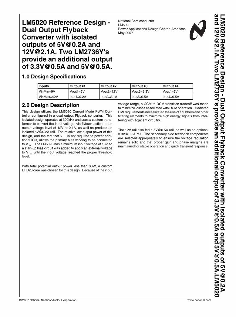
LM5020 Reference Design -Dual Output FlybackConverter with isolatedoutputs of [email protected] [email protected]. Two LM2736Y'sprovide an additional outputof [email protected] and [email protected].
National SemiconductorLM5020Power Applications Design Center, AmericasMay 2007
1.0 Design Specifications
Inputs Output #1 Output #2 Output #3 Output #4
VinMin=9V Vout1=5V Vout2=12V Vout3=3.3V Vout4=5V
VinMax=42V Iout1=0.2A Iout2=2.1A Iout3=0.5A Iout4=0.5A
2.0 Design DescriptionThis design utilizes the LM5020 Current Mode PWM Con-troller configured in a dual output Flyback converter. Thisisolated design operates at 300kHz and uses a custom trans-former to convert the input voltage, via flyback action, to anoutput voltage level of 12V at 2.1A, as well as produce anisolated [email protected] rail. The relative low output power of thisdesign, and the fact that V cc is not required to power addi-tional IC’s, allows the primary bias winding to be connectedto V in . The LM5020 has a minimum input voltage of 13V soa start-up bias circuit was added to apply an external voltageto V cc until the input voltage reached the proper thresholdlevel.
With total potential output power less than 30W, a customEFD20 core was chosen for this design. Because of the input
voltage range, a CCM to DCM transition tradeoff was madeto minimize losses associated with DCM operation. RadiatedEMI requirements necessitated the use of snubbers and otherfiltering elements to minimize high energy signals from inter-fering with adjacent circuitry.
The 12V rail also fed a [email protected] rail, as well as an [email protected] rail. The secondary side feedback componentsare selected appropriately to ensure the voltage regulationremains solid and that proper gain and phase margins aremaintained for stable operation and quick transient response.
© 2007 National Semiconductor Corporation www.national.com
LM
5020 R
efe
ren
ce D
esig
n - D
ual O
utp
ut F
lyb
ack C
on
verte
r with
iso
late
d o
utp
uts
of 5
V@
0.2
Aan
d 1
2V
@2.1
A. T
wo
LM
2736Y
's p
rovid
e a
n a
dd
ition
al o
utp
ut o
f 3.3
V@
0.5
A a
nd
5V
@0.5
A.L
M5020
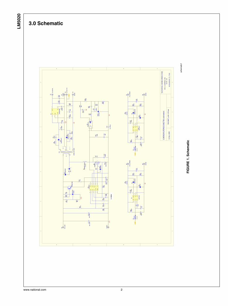
3.0 Schematic
12
34
56
ABCD
65
43
21
D C B A
NA
TIO
NA
L SE
MIC
ON
DU
CTO
R
801
E. C
AM
PBEL
L R
D.
SUIT
E 5
25
RIC
HA
RD
SON
, TX
750
81
LM50
20/L
P299
2/LM
2736
con
verte
rs
13-D
ec-2
005
NSC
0607
_with
3.3
Vou
t
R11
21.0
kC
90.
01u
C10
100p
R12
2.00
k
C13
2.2u
F
P1
9V to
42V
PG
ND
1
P3
5V @
0.2
A
P5
SGN
D1
C8
1uF
, 100
V
C15
10n
R13 10
fs=3
00kH
z
Vin
1
VFB
2
com
p3
Vcc
4
out
5G
ND
6
UV
LO7
CS
8
RT
9
SS10
U1
LM
5020
-1
C12
0.1u
R8
2.49
k
R9
10.7
k
R16
1.00
k
Q2
SI44
86E
Y
R5
OP
EN
C1
OP
EN
D1
MM
SD41
48
1 234
U2
PS25
01-1
-L
C16
1n, 2
50V
ac
C14
100p
F
R7
10
D4
36V
R18
499
C18
0.04
7u
C11
100p
R17
499
C17
0.47
u
RE
F2
LM
V43
1
R20
10.0
k
R19
100
R2
10k
R10
10k
R1
78.7
k
RE
F1
LM
V43
1
D5
MU
RS1
10T
3
R6
OP
EN
C2
OP
EN
D6
MU
RS2
20T
3
P4
12V
@ 2
.1A
R23
86.6
k
+12V
R15
0.05
, 0.1
W
79 610
4,5
T10
EFD
15-3
F3-A
63S
Np
= 7t
Ns1
= 7
t
Ns2
= 4
t
P2
SGN
D2
C5
1uF
C4
1uF
Boo
st1
Gnd
2
FB3
EN4
Vin
5
SW6
U4
LM
2736
-YR
2210
.0k
R25
30.1
k
C20
0.01
u
C24
1u
L4
47uH
+12V
P9
SGN
D1
P7
5V
@ 5
00m
A
D3
MM
SD41
48C
224.
7uR
410
0k
D8
B13
0
+C
315
0uF
+C
668
0uF
Boo
st1
Gnd
2
FB3
EN4
Vin
5
SW6
U3
LM
2736
-YR
2110
.0k
R24
16.5
k
C19
0.01
u
C23
1u
L3
47uH
+12V
P8
SGN
D1
P6
3.3V
@ 5
00m
A
D2
MM
SD41
48C
214.
7uR
3
100k
D7
B13
0
R14 0L1
FE
RR
ITE
BE
AD
(Opt
iona
l)(O
ptio
nal)
(Opt
iona
l)
C7
1uF
, 100
V
C25
OP
EN
C26
OP
EN
R27
OP
EN
R26
OP
EN
L2
10uH
160
8
L5
10uH
160
8
Q1
MM
BT
3904
Vin
1
gnd
2
on/o
ff3
VO
UT
5
bp4
U5 LP2
992A
IM5 C27
0.01
uF
+C
2822
uFC
2910
uF
R28
806
D9
OP
EN
R29
10k
schem
atic
1
FIG
UR
E 1
. S
ch
em
ati
c
www.national.com 2
LM
5020
4.0 Bill of Materials
3 www.national.com
LM
5020
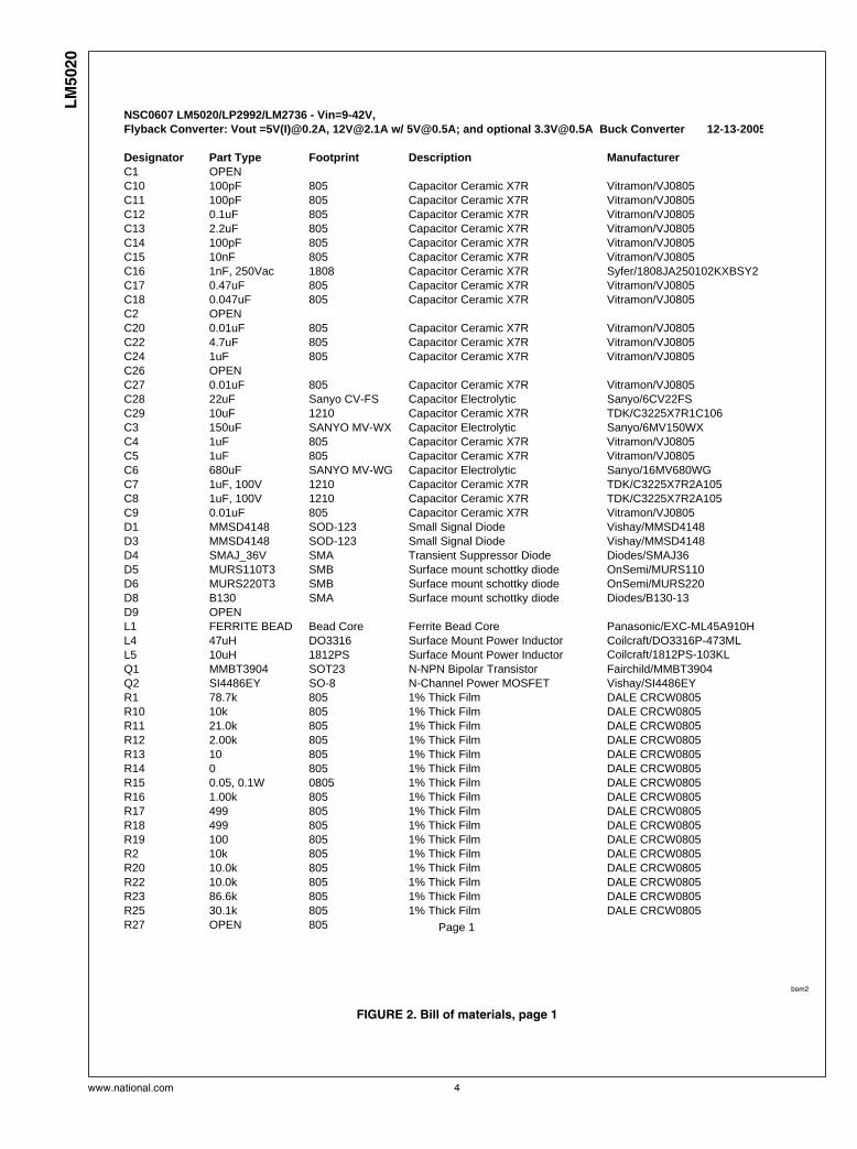
NSC0607 LM5020/LP2992/LM2736 - Vin=9-42V,Flyback Converter: Vout =5V(I)@0.2A, [email protected] w/ [email protected]; and optional [email protected] Buck Converter 12-13-2005
Designator Part Type Footprint Description ManufacturerC1 OPENC10 100pF 805 Capacitor Ceramic X7R Vitramon/VJ0805C11 100pF 805 Capacitor Ceramic X7R Vitramon/VJ0805C12 0.1uF 805 Capacitor Ceramic X7R Vitramon/VJ0805C13 2.2uF 805 Capacitor Ceramic X7R Vitramon/VJ0805C14 100pF 805 Capacitor Ceramic X7R Vitramon/VJ0805C15 10nF 805 Capacitor Ceramic X7R Vitramon/VJ0805C16 1nF, 250Vac 1808 Capacitor Ceramic X7R Syfer/1808JA250102KXBSY2C17 0.47uF 805 Capacitor Ceramic X7R Vitramon/VJ0805C18 0.047uF 805 Capacitor Ceramic X7R Vitramon/VJ0805C2 OPENC20 0.01uF 805 Capacitor Ceramic X7R Vitramon/VJ0805C22 4.7uF 805 Capacitor Ceramic X7R Vitramon/VJ0805C24 1uF 805 Capacitor Ceramic X7R Vitramon/VJ0805C26 OPENC27 0.01uF 805 Capacitor Ceramic X7R Vitramon/VJ0805C28 22uF Sanyo CV-FS Capacitor Electrolytic Sanyo/6CV22FSC29 10uF 1210 Capacitor Ceramic X7R TDK/C3225X7R1C106C3 150uF SANYO MV-WX Capacitor Electrolytic Sanyo/6MV150WXC4 1uF 805 Capacitor Ceramic X7R Vitramon/VJ0805C5 1uF 805 Capacitor Ceramic X7R Vitramon/VJ0805C6 680uF SANYO MV-WG Capacitor Electrolytic Sanyo/16MV680WGC7 1uF, 100V 1210 Capacitor Ceramic X7R TDK/C3225X7R2A105C8 1uF, 100V 1210 Capacitor Ceramic X7R TDK/C3225X7R2A105C9 0.01uF 805 Capacitor Ceramic X7R Vitramon/VJ0805D1 MMSD4148 SOD-123 Small Signal Diode Vishay/MMSD4148D3 MMSD4148 SOD-123 Small Signal Diode Vishay/MMSD4148D4 SMAJ_36V SMA Transient Suppressor Diode Diodes/SMAJ36D5 MURS110T3 SMB Surface mount schottky diode OnSemi/MURS110D6 MURS220T3 SMB Surface mount schottky diode OnSemi/MURS220D8 B130 SMA Surface mount schottky diode Diodes/B130-13D9 OPENL1 FERRITE BEAD Bead Core Ferrite Bead Core Panasonic/EXC-ML45A910HL4 47uH DO3316 Surface Mount Power Inductor Coilcraft/DO3316P-473MLL5 10uH 1812PS Surface Mount Power Inductor Coilcraft/1812PS-103KLQ1 MMBT3904 SOT23 N-NPN Bipolar Transistor Fairchild/MMBT3904Q2 SI4486EY SO-8 N-Channel Power MOSFET Vishay/SI4486EYR1 78.7k 805 1% Thick Film DALE CRCW0805R10 10k 805 1% Thick Film DALE CRCW0805R11 21.0k 805 1% Thick Film DALE CRCW0805R12 2.00k 805 1% Thick Film DALE CRCW0805R13 10 805 1% Thick Film DALE CRCW0805R14 0 805 1% Thick Film DALE CRCW0805R15 0.05, 0.1W 0805 1% Thick Film DALE CRCW0805R16 1.00k 805 1% Thick Film DALE CRCW0805R17 499 805 1% Thick Film DALE CRCW0805R18 499 805 1% Thick Film DALE CRCW0805R19 100 805 1% Thick Film DALE CRCW0805R2 10k 805 1% Thick Film DALE CRCW0805R20 10.0k 805 1% Thick Film DALE CRCW0805R22 10.0k 805 1% Thick Film DALE CRCW0805R23 86.6k 805 1% Thick Film DALE CRCW0805R25 30.1k 805 1% Thick Film DALE CRCW0805R27 OPEN 805 Page 1
bom2
FIGURE 2. Bill of materials, page 1
www.national.com 4
LM
5020
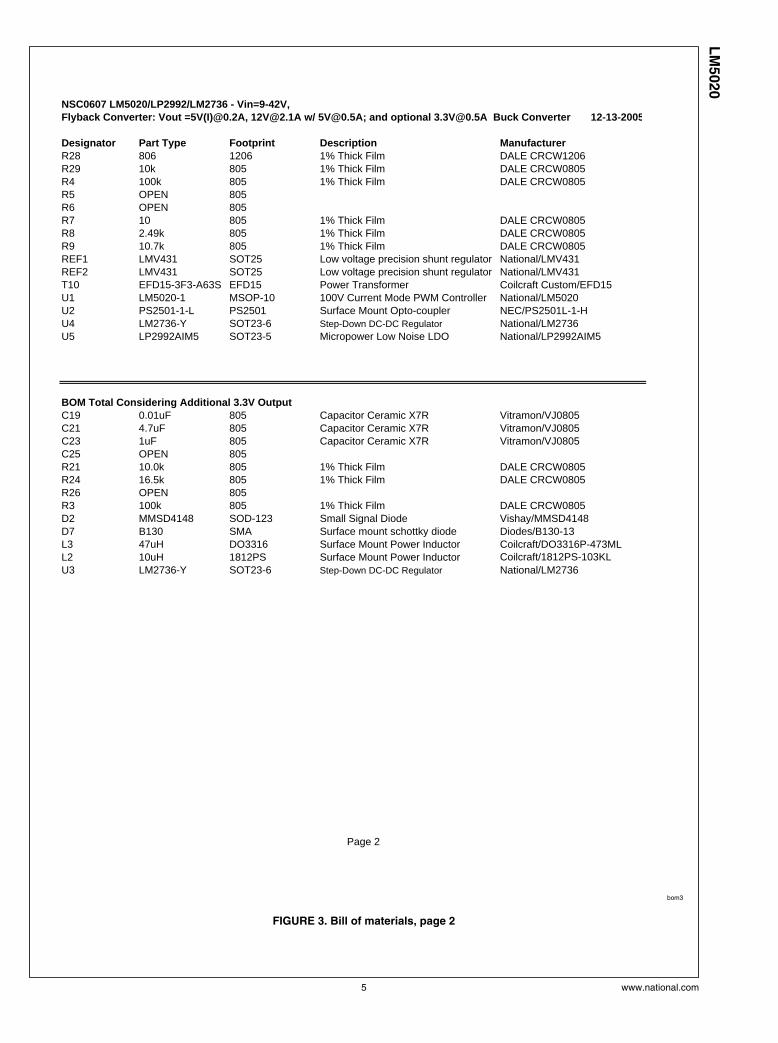
NSC0607 LM5020/LP2992/LM2736 - Vin=9-42V,Flyback Converter: Vout =5V(I)@0.2A, [email protected] w/ [email protected]; and optional [email protected] Buck Converter 12-13-2005
Designator Part Type Footprint Description ManufacturerR28 806 1206 1% Thick Film DALE CRCW1206R29 10k 805 1% Thick Film DALE CRCW0805R4 100k 805 1% Thick Film DALE CRCW0805R5 OPEN 805R6 OPEN 805R7 10 805 1% Thick Film DALE CRCW0805R8 2.49k 805 1% Thick Film DALE CRCW0805R9 10.7k 805 1% Thick Film DALE CRCW0805REF1 LMV431 SOT25 Low voltage precision shunt regulator National/LMV431REF2 LMV431 SOT25 Low voltage precision shunt regulator National/LMV431T10 EFD15-3F3-A63S EFD15 Power Transformer Coilcraft Custom/EFD15U1 LM5020-1 MSOP-10 100V Current Mode PWM Controller National/LM5020U2 PS2501-1-L PS2501 Surface Mount Opto-coupler NEC/PS2501L-1-HU4 LM2736-Y SOT23-6 Step-Down DC-DC Regulator National/LM2736U5 LP2992AIM5 SOT23-5 Micropower Low Noise LDO National/LP2992AIM5
BOM Total Considering Additional 3.3V Output C19 0.01uF 805 Capacitor Ceramic X7R Vitramon/VJ0805C21 4.7uF 805 Capacitor Ceramic X7R Vitramon/VJ0805C23 1uF 805 Capacitor Ceramic X7R Vitramon/VJ0805C25 OPEN 805R21 10.0k 805 1% Thick Film DALE CRCW0805R24 16.5k 805 1% Thick Film DALE CRCW0805R26 OPEN 805R3 100k 805 1% Thick Film DALE CRCW0805D2 MMSD4148 SOD-123 Small Signal Diode Vishay/MMSD4148D7 B130 SMA Surface mount schottky diode Diodes/B130-13L3 47uH DO3316 Surface Mount Power Inductor Coilcraft/DO3316P-473MLL2 10uH 1812PS Surface Mount Power Inductor Coilcraft/1812PS-103KLU3 LM2736-Y SOT23-6 Step-Down DC-DC Regulator National/LM2736
Page 2
bom3
FIGURE 3. Bill of materials, page 2
5 www.national.com
LM
5020
5.0 Other Operating Values
Operating Values
Description Parameter Value Unit
Modulation Frequency Frequency 300 KHz
Total output power Pout 30 W
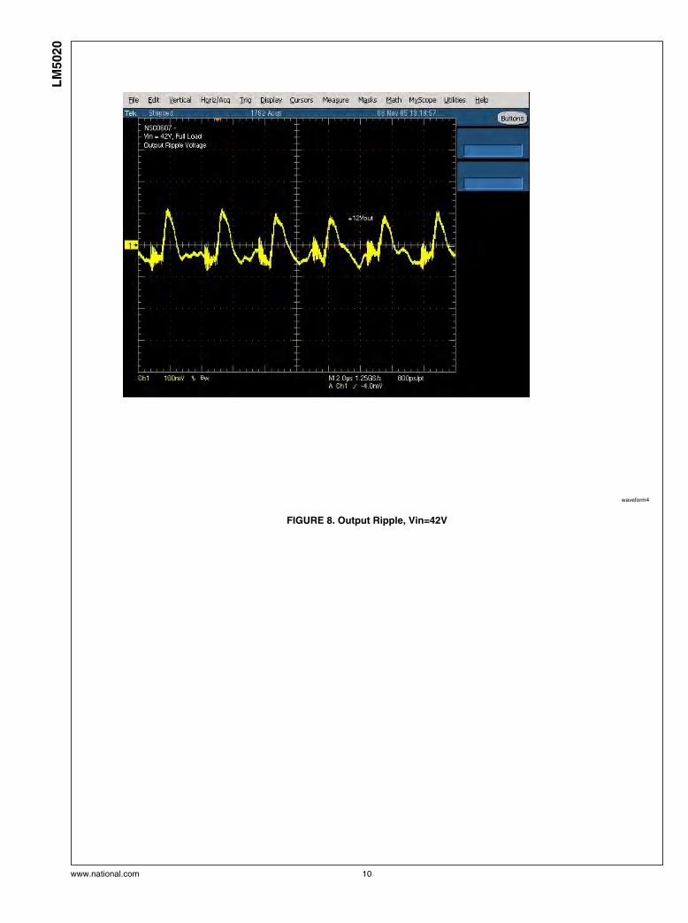
Peak to peak ripple voltage, 9Vin with full load Vout p-p 250 mV
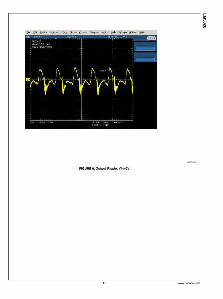
Peak to peak ripple voltage, 42Vin with full load Vout p-p 200 mV
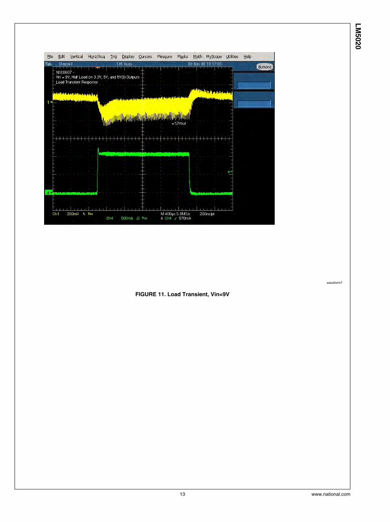
Dynamic Load Regulation, Vin = 9V, half load on 3.3V, 5V, Outputs, full load step Dynamic Load 400 mV
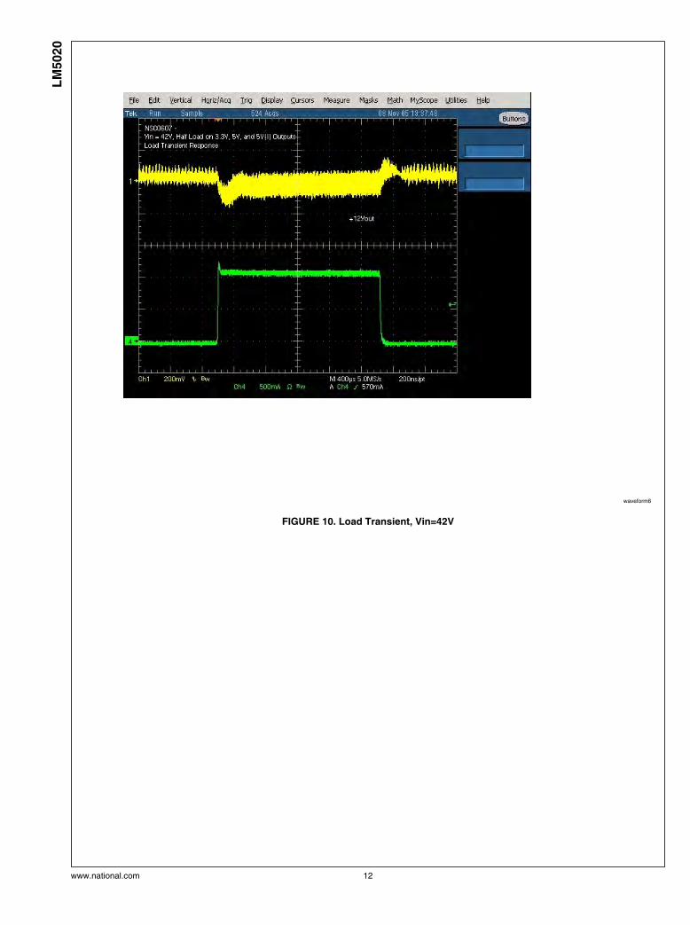
Dynamic Load Regulation, Vin = 42V, half load on 3.3V, 5V, Outputs, full load step Dynamic Load 300 mV
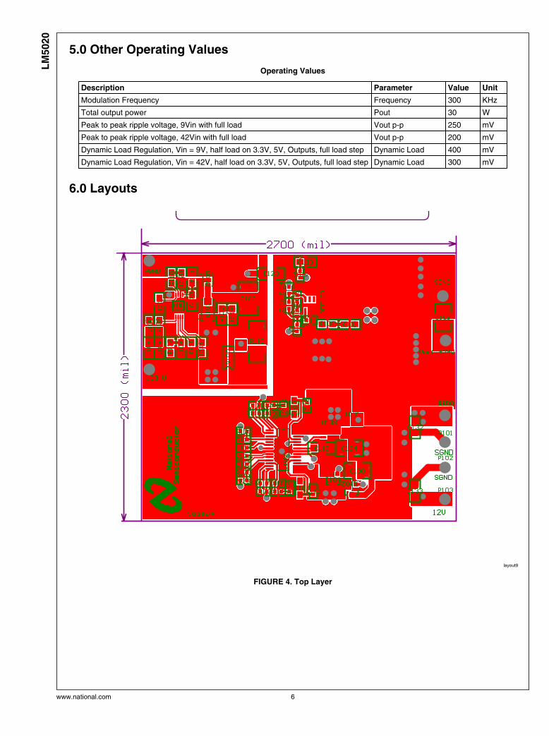
6.0 Layouts
layout9
FIGURE 4. Top Layer
www.national.com 6
LM
5020
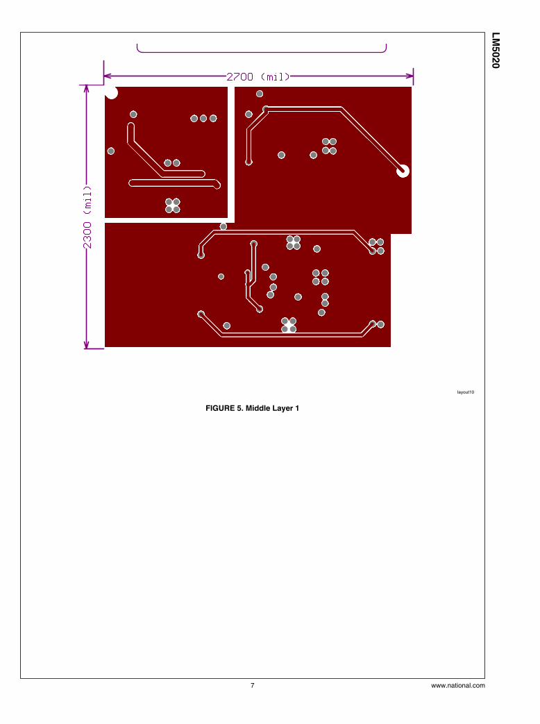
layout10
FIGURE 5. Middle Layer 1
7 www.national.com
LM
5020
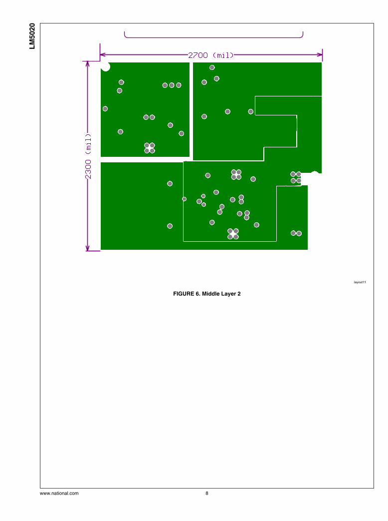
layout11
FIGURE 6. Middle Layer 2
www.national.com 8
LM
5020
layout12
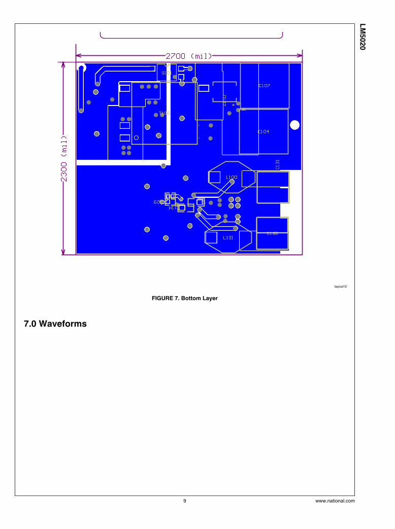
FIGURE 7. Bottom Layer
7.0 Waveforms
9 www.national.com
LM
5020
waveform4
FIGURE 8. Output Ripple, Vin=42V
www.national.com 10
LM
5020
waveform5
FIGURE 9. Output Ripple, Vin=9V
11 www.national.com
LM
5020
waveform6
FIGURE 10. Load Transient, Vin=42V
www.national.com 12
LM
5020
waveform7
FIGURE 11. Load Transient, Vin=9V
13 www.national.com
LM
5020
waveform
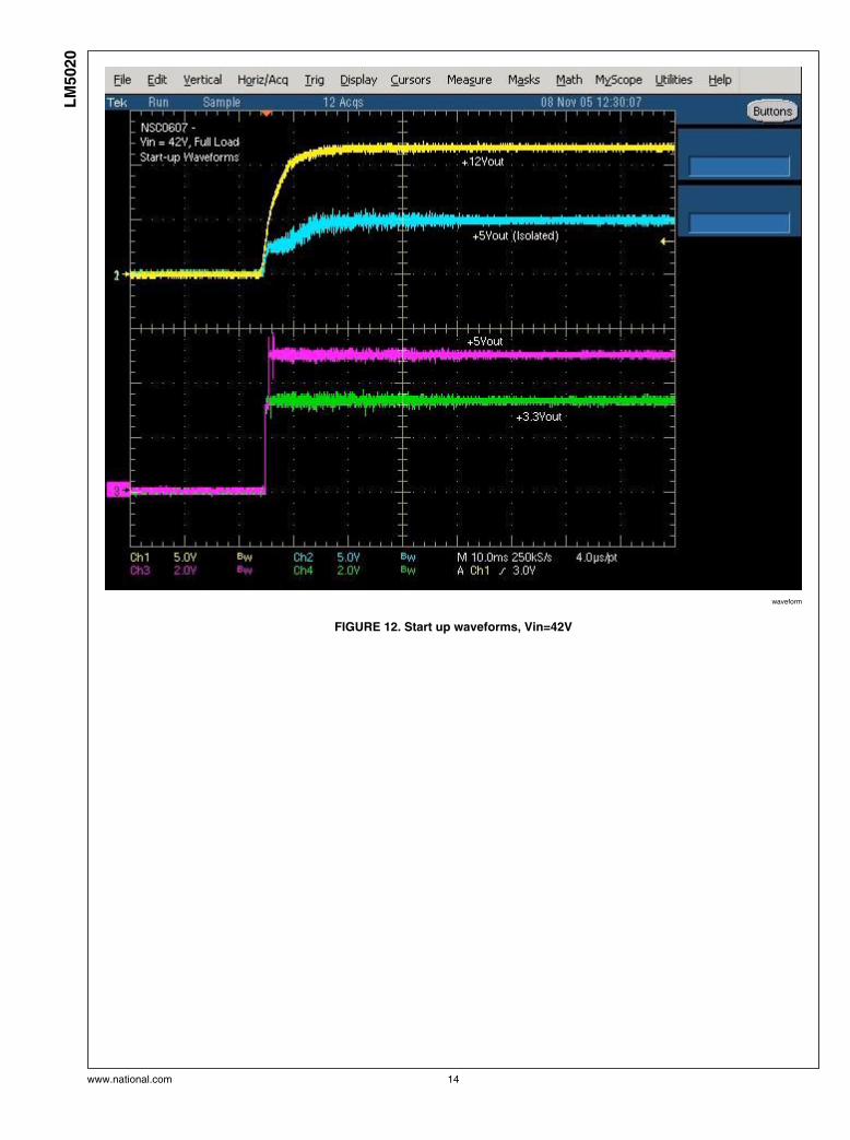
FIGURE 12. Start up waveforms, Vin=42V
www.national.com 14
LM
5020
waveform8
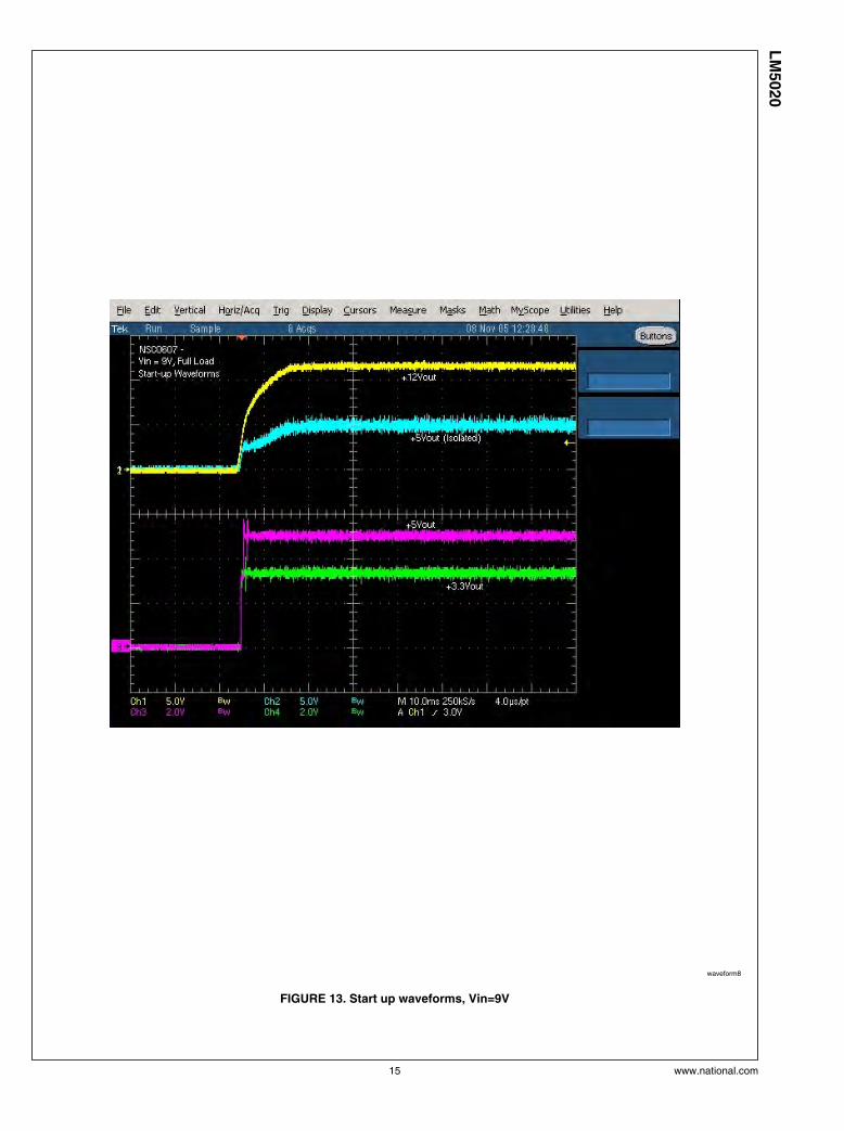
FIGURE 13. Start up waveforms, Vin=9V
15 www.national.com
LM
5020
waveform9
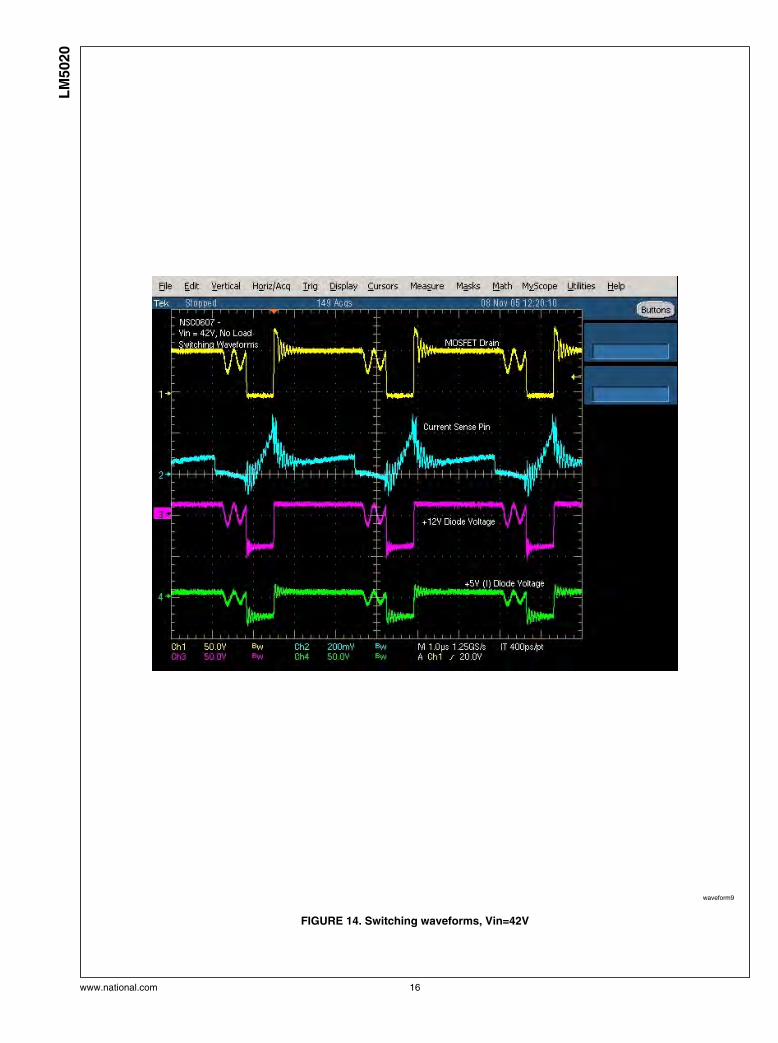
FIGURE 14. Switching waveforms, Vin=42V
www.national.com 16
LM
5020
waveform10
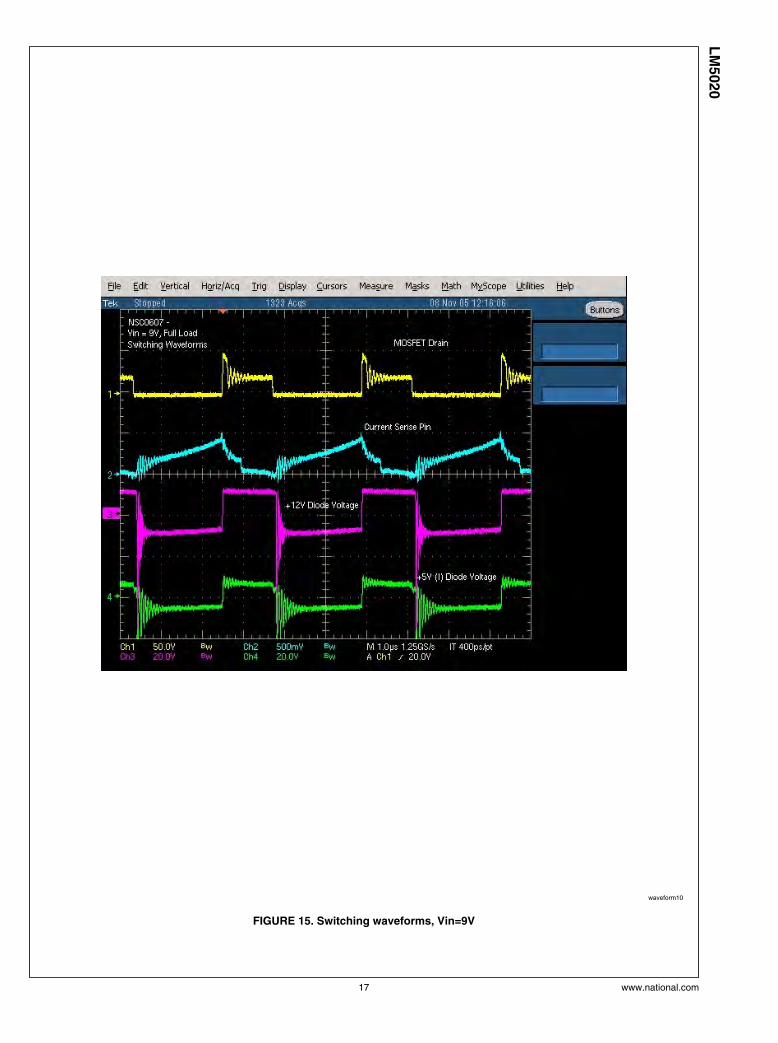
FIGURE 15. Switching waveforms, Vin=9V
17 www.national.com
LM
5020
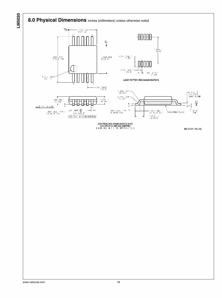
8.0 Physical Dimensions inches (millimeters) unless otherwise noted
www.national.com 18
LM
5020

Notes
19 www.national.com
LM
5020
Notes
LM
5020
LM
5020 R
efe
ren
ce D
esig
n -
Du
al O
utp
ut
Fly
back C
on
vert
er
wit
h iso
late
do
utp
uts
of
5V
@0.2
A a
nd
12V
@2.1
A. T
wo
LM
2736Y
's p
rovid
e a
n a
dd
itio
nal
ou
tpu
t o
f 3.3
V@
0.5
A a
nd
5V
@0.5
A.
National Semiconductor's design tools attempt to recreate the performance of a substantially equivalent physical implementation of thedesign. Reference designs are created using National's published specifications as well as the published specifications of other devicemanufacturers. While National does update this information periodically, this information may not be current at the time the referencedesign is built. National and/or its licensors do not warrant the accuracy or completeness of the specifications or any information containedtherein. National and/or its licensors do not warrant that any designs or recommended parts will meet the specifications you entered, willbe suitable for your application or fit for any particular purpose, or will operate as shown in the simulation in a physical implementation.National and/or its licensors do not warrant that the designs are production worthy. You should completely validate and test your designimplementation to confirm the system functionality for your application.
National does not assume any responsibility for use of any circuitry described, no circuit patent licenses are implied and National reservesthe right at any time without notice to change said circuitry and specifications.
For the most current product information visit us at www.national.com.
LIFE SUPPORT POLICY
NATIONAL'S PRODUCTS ARE NOT AUTHORIZED FOR USE AS CRITICAL COMPONENTS IN LIFE SUPPORT DEVICES OR SYS-TEMS WITHOUT THE EXPRESS WRITTEN APPROVAL OF THE PRESIDENT AND GENERAL COUNSEL OF NATIONAL SEMICON-DUCTOR CORPORATION. As used herein:
1. Life support devices or systems are devices or systems which,(a) are intended for surgical implant into the body, or (b) supportor sustain life, and whose failure to perform when properly usedin accordance with instructions for use provided in the labeling,can be reasonably expected to result in a significant injury tothe user.
2. A critical component is any component of a life support deviceor system whose failure to perform can be reasonably expectedto cause the failure of the life support device or system, or toaffect its safety or effectiveness.
BANNED SUBSTANCE COMPLIANCE
National Semiconductor certifies that the products and packing materials meet the provisions of the Customer Products StewardshipSpecification (CSP-9-111C2) and the Banned Substances and Materials of Interest Specification (CSP-9-111S2) and contain no "BannedSubstances" as defined in CSP-9-111S2.
Leadfree products are RoHS compliant.
National SemiconductorAmericas CustomerSupport CenterEmail:[email protected]: 1-800-272-9959
National Semiconductor EuropeCustomer Support CenterFax: +49 (0) 180-530-85-86Email: [email protected] Tel: +49 (0) 69 9508 6208English Tel: +49 (0) 870 24 0 2171Français Tel: +33 (0) 1 41 91 8790
National Semiconductor AsiaPacific Customer Support CenterEmail: [email protected]
National Semiconductor JapanCustomer Support CenterFax: 81-3-5639-7507Email: [email protected]: 81-3-5639-7560
www.national.com

IMPORTANT NOTICE
Texas Instruments Incorporated and its subsidiaries (TI) reserve the right to make corrections, modifications, enhancements, improvements,and other changes to its products and services at any time and to discontinue any product or service without notice. Customers shouldobtain the latest relevant information before placing orders and should verify that such information is current and complete. All products aresold subject to TI’s terms and conditions of sale supplied at the time of order acknowledgment.
TI warrants performance of its hardware products to the specifications applicable at the time of sale in accordance with TI’s standardwarranty. Testing and other quality control techniques are used to the extent TI deems necessary to support this warranty. Except wheremandated by government requirements, testing of all parameters of each product is not necessarily performed.
TI assumes no liability for applications assistance or customer product design. Customers are responsible for their products andapplications using TI components. To minimize the risks associated with customer products and applications, customers should provideadequate design and operating safeguards.
TI does not warrant or represent that any license, either express or implied, is granted under any TI patent right, copyright, mask work right,or other TI intellectual property right relating to any combination, machine, or process in which TI products or services are used. Informationpublished by TI regarding third-party products or services does not constitute a license from TI to use such products or services or awarranty or endorsement thereof. Use of such information may require a license from a third party under the patents or other intellectualproperty of the third party, or a license from TI under the patents or other intellectual property of TI.
Reproduction of TI information in TI data books or data sheets is permissible only if reproduction is without alteration and is accompaniedby all associated warranties, conditions, limitations, and notices. Reproduction of this information with alteration is an unfair and deceptivebusiness practice. TI is not responsible or liable for such altered documentation. Information of third parties may be subject to additionalrestrictions.
Resale of TI products or services with statements different from or beyond the parameters stated by TI for that product or service voids allexpress and any implied warranties for the associated TI product or service and is an unfair and deceptive business practice. TI is notresponsible or liable for any such statements.
TI products are not authorized for use in safety-critical applications (such as life support) where a failure of the TI product would reasonablybe expected to cause severe personal injury or death, unless officers of the parties have executed an agreement specifically governingsuch use. Buyers represent that they have all necessary expertise in the safety and regulatory ramifications of their applications, andacknowledge and agree that they are solely responsible for all legal, regulatory and safety-related requirements concerning their productsand any use of TI products in such safety-critical applications, notwithstanding any applications-related information or support that may beprovided by TI. Further, Buyers must fully indemnify TI and its representatives against any damages arising out of the use of TI products insuch safety-critical applications.
TI products are neither designed nor intended for use in military/aerospace applications or environments unless the TI products arespecifically designated by TI as military-grade or "enhanced plastic." Only products designated by TI as military-grade meet militaryspecifications. Buyers acknowledge and agree that any such use of TI products which TI has not designated as military-grade is solely atthe Buyer's risk, and that they are solely responsible for compliance with all legal and regulatory requirements in connection with such use.
TI products are neither designed nor intended for use in automotive applications or environments unless the specific TI products aredesignated by TI as compliant with ISO/TS 16949 requirements. Buyers acknowledge and agree that, if they use any non-designatedproducts in automotive applications, TI will not be responsible for any failure to meet such requirements.
Following are URLs where you can obtain information on other Texas Instruments products and application solutions:
Products Applications
Audio www.ti.com/audio Automotive and Transportation www.ti.com/automotive
Amplifiers amplifier.ti.com Communications and Telecom www.ti.com/communications
Data Converters dataconverter.ti.com Computers and Peripherals www.ti.com/computers
DLP® Products www.dlp.com Consumer Electronics www.ti.com/consumer-apps
DSP dsp.ti.com Energy and Lighting www.ti.com/energy
Clocks and Timers www.ti.com/clocks Industrial www.ti.com/industrial
Interface interface.ti.com Medical www.ti.com/medical
Logic logic.ti.com Security www.ti.com/security
Power Mgmt power.ti.com Space, Avionics and Defense www.ti.com/space-avionics-defense
Microcontrollers microcontroller.ti.com Video and Imaging www.ti.com/video
RFID www.ti-rfid.com
OMAP Mobile Processors www.ti.com/omap
Wireless Connectivity www.ti.com/wirelessconnectivity
TI E2E Community Home Page e2e.ti.com
Mailing Address: Texas Instruments, Post Office Box 655303, Dallas, Texas 75265Copyright © 2012, Texas Instruments Incorporated