Dual line IPAD , common mode filter with ESD protection ... · Dual line IPAD™, common mode...
13
This is information on a product in full production. March 2014 DocID018656 Rev 2 1/13 ECMF02-2BF3 Dual line IPAD™, common mode filter with ESD protection for high speed serial interface Datasheet - production data Features • Very large differential bandwidth above 5 GHz • High common mode attenuation: – - 23 dB at 900 MHz. • High common mode attenuation: – - 20 dB between 800 MHz and 2.2 GHz. • Very low PCB space consumption: <1.1mm 2 • Thin package: 0.50 mm max. after reflow • Lead-free package • High reduction of parasitic elements through integration Complies with the following standard: • IEC 61000-4-2 level 4 input and output pins: – ±15 kV (air discharge) – ±8 kV (contact discharge) Application High speed serial interfaces such as USB 2.0, MIPI D-PHY, MDDI and HDMI. Description The ECMF02-2BF3 is a highly integrated common mode filter designed to suppress EMI/RFI common mode noise on high speed differential serial buses like MIPI D-PHY, MDDI, USB 2.0 and HDMI. The ECMF02-2BF3 can protect and filter one differential lane. Figure 1. Pin configuration (bump side) Figure 2. Schematic TM: IPAD is a trademark of STMicroelectronics. Flip Chip 5 bumps 1 2 A B C IN1 IN2 GND OUT1 OUT2 IN1 IN2 OUT1 OUT2 GND GND www.st.com
Transcript of Dual line IPAD , common mode filter with ESD protection ... · Dual line IPAD™, common mode...

This is information on a product in full production.
March 2014 DocID018656 Rev 2 1/13
ECMF02-2BF3
Dual line IPAD™, common mode filter withESD protection for high speed serial interface
Datasheet - production data
Features
• Very large differential bandwidth above 5 GHz
• High common mode attenuation:
– - 23 dB at 900 MHz.
• High common mode attenuation:
– - 20 dB between 800 MHz and 2.2 GHz.
• Very low PCB space consumption: <1.1mm2
• Thin package: 0.50 mm max. after reflow
• Lead-free package
• High reduction of parasitic elements through integration
Complies with the following standard:
• IEC 61000-4-2 level 4 input and output pins:
– ±15 kV (air discharge)
– ±8 kV (contact discharge)
Application
High speed serial interfaces such as USB 2.0, MIPI D-PHY, MDDI and HDMI.
Description
The ECMF02-2BF3 is a highly integrated common mode filter designed to suppress EMI/RFI common mode noise on high speed differential serial buses like MIPI D-PHY, MDDI, USB 2.0 and HDMI.
The ECMF02-2BF3 can protect and filter one differential lane.
Figure 1. Pin configuration (bump side)
Figure 2. Schematic
TM: IPAD is a trademark of STMicroelectronics.
Flip Chip5 bumps
12
A
B
C
IN1
IN2
GND
OUT1
OUT2
IN1
IN2
OUT1
OUT2
GND
GND
www.st.com

Characteristics ECMF02-2BF3
2/13 DocID018656 Rev 2
1 Characteristics
Figure 3. Electrical characteristics (definitions)
Table 1. Absolute maximum ratings (Tamb = 25 °C)
Symbol Parameter Value Unit
VPP Peak pulse voltage(1)
1. Measurements done on IEC 61000-4-2 test bench. For further details see Application note AN3353.
IEC 61000-4-2 contact discharge
IEC 61000-4-2 air discharge
10
20kV
Tj Maximum junction temperature 125 °C
Top Operating temperature range - 30 to + 85 °C
Tstg Storage temperature range - 55 to 150 °C
Table 2. Electrical characteristics (values, Tamb = 25 °C)
Symbol Test conditions Min. Typ. Max. Unit
VBR IR = 1 mA 6 V
IRM VRM = 3 V per line 100 nA
RDC DC serial resistance 3 4 Ω
Symbol ParameterV = Breakdown voltage
I
I
= Leakage current @
= Leakage current @
V
VV = Stand-off voltage
BR
RM
R
RM
BR
RM
I
VVBRVRM
IRIRM
IRM
IR
VRMVBR

DocID018656 Rev 2 3/13
ECMF02-2BF3 Application schematics
13
2 Application schematics
Figure 4. USB2.0 application
Figure 5. MIPI D-PHY application
ECMF02-2BF3
D-
D+
GND
To U
SB
tra
nsc
eive
r
ID
VBUS
IN1
GND
OUT1
OUT2 IN2
D0+
D0-
D1+
D1 -
D2+
D2-
CLK+
CLK-
GND
GND
GND
GND
IN1
GND
OUT1
OUT2 IN2
IN1
GND
OUT1
OUT2 IN2
IN1
GND
OUT1
OUT2 IN2
IN1
GND
OUT1
OUT2 IN2
To d
isp
lay
and
cam
era
MIP
I D-P
HY
Measurement curves ECMF02-2BF3
4/13 DocID018656 Rev 2
3 Measurement curves
Figure 6. SDD21 differential attenuation measurement (Z0 diff = 100 Ω)
Figure 7. SCC21 common mode attenuation measurement (Z0 com = 50 Ω)
100.0k 1.0M 10.0M 100.0M 1.0G-3.00
-2.50
-2.00
-1.50
-1.00
-0.50
0.00SDD21 (dB)
F (Hz)
SCC21 (dB)
100.0k 1.0M 10.0M 100.0M 1.0G-40.00
-35.00
-30.00
-25.00
-20.00
-15.00
-10.00
-5.00
0.00
F (Hz)

DocID018656 Rev 2 5/13
ECMF02-2BF3 Measurement curves
13
Figure 8. SDD11 and SDD22 differential return loss measurement (Z0 diff = 100 Ω)
100.0k 1.0M 10.0M 100.0M 1.0G-40.00
-35.00
-30.00
-25.00
-20.00
-15.00
-10.00
-5.00
0.00
SDD11 SDD22
SDD1 and SDD22 (dB)
F (Hz)
Measurement curves ECMF02-2BF3
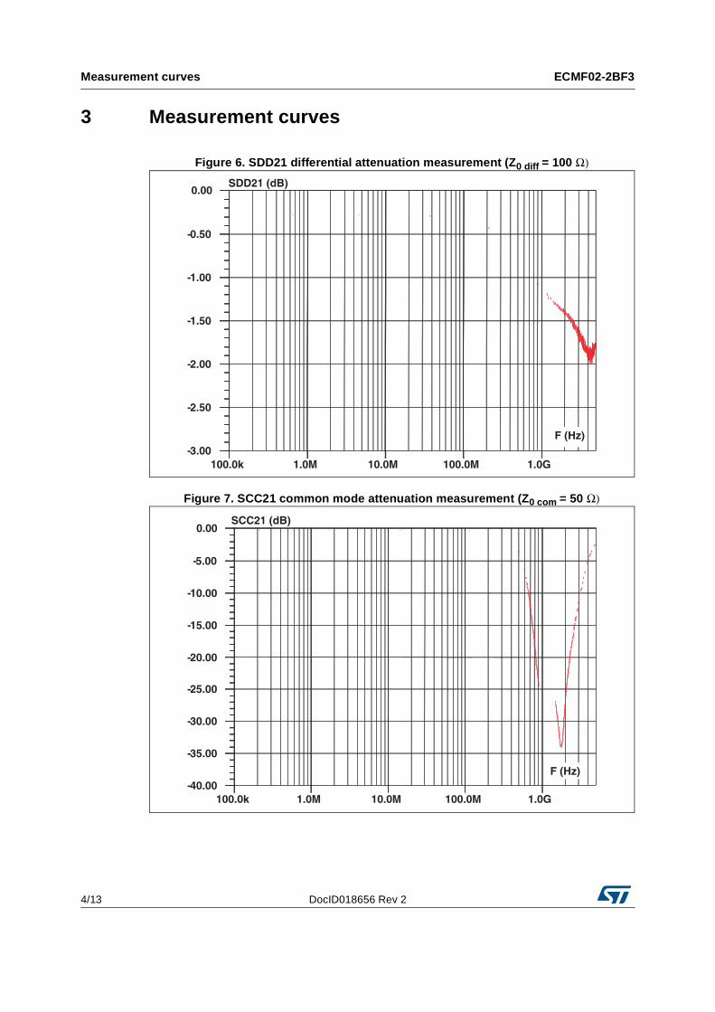
6/13 DocID018656 Rev 2
Figure 9. ESD response to IEC 61000-4-2 (+8 kV contact discharge)
Figure 10. ESD response to IEC 61000-4-2 (-8 kV contact discharge)
61.2 V
31.8 V
19.6 V 16.4 V
1
2
43
V : ESD peak voltageV :clamping voltage @ 30 nsV :clamping voltage @ 60 ns
PP
CL
CL
V :clamping voltage @ 100 nsCL
1234
-60.6 V
-21.9 V-16.7 V -13.7 V
1
243
V : ESD peak voltageV :clamping voltage @ 30 nsV :clamping voltage @ 60 ns
PP
CL
CL
V :clamping voltage @ 100 nsCL
1234
DocID018656 Rev 2 7/13
ECMF02-2BF3 High speed differential standard compliance tests
13
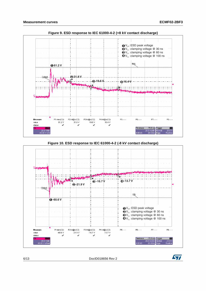
4 High speed differential standard compliance tests
4.1 USB2.0 compliance tests
Figure 11. TDR measurement (loaded by Zdiff = 90 Ω)
Figure 12. Eye diagram with USB2.0 template
70
75
80
85
90
95
100
110
0.5 1.0 1.5 2.0 2.5 3.0 3.5
ZDIFF ( )Ω
t(ns)
0.0
105
tr = 400 ps (10% - 90%)
200 mV/div 200 mV/div
347.2 ps/div347.2 ps/div
Through ISS* Board + ECMF02-2BF3
* Impedance standard substrate

High speed differential standard compliance tests ECMF02-2BF3
8/13 DocID018656 Rev 2
4.2 HDMI1.4 compliance tests
Figure 13. TDR measurement (loaded by Zdiff = 100 Ω), tr = 194 ps (10% - 90%)
DocID018656 Rev 2 9/13
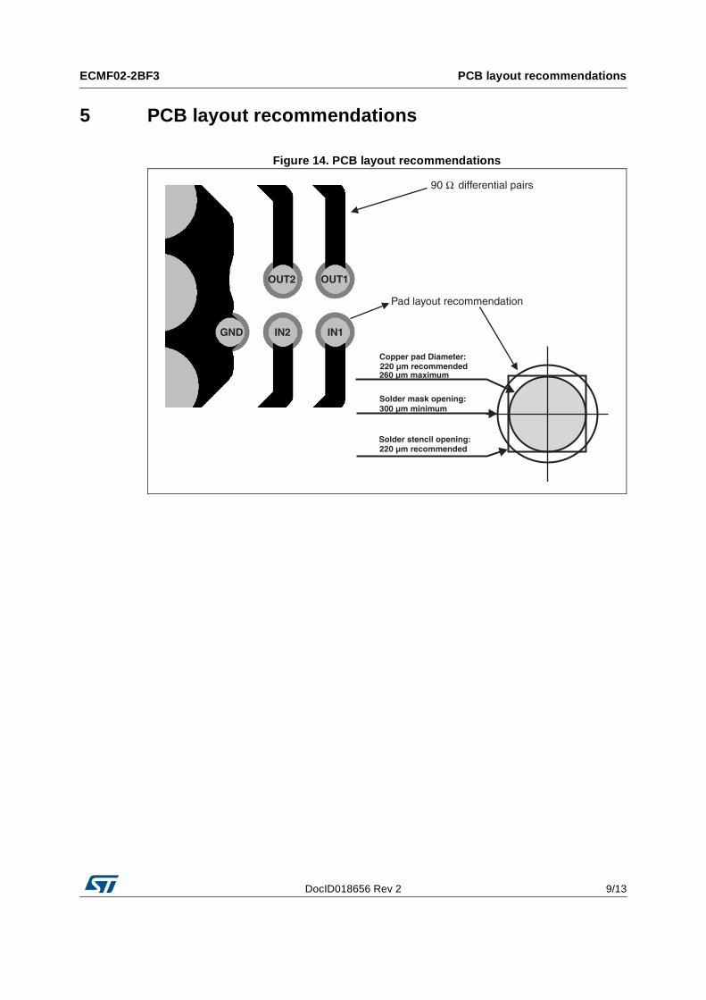
ECMF02-2BF3 PCB layout recommendations
13
5 PCB layout recommendations
Figure 14. PCB layout recommendations
90 Ω differential pairs
Pad layout recommendation
GND IN2 IN1
OUT2 OUT1
220 µm recommended
220 µm recommended260 µm maximum
Solder stencil opening:
Copper pad Diameter:
Solder mask opening:300 µm minimum

Package information ECMF02-2BF3
10/13 DocID018656 Rev 2
6 Package information
In order to meet environmental requirements, ST offers these devices in different grades of ECOPACK® packages, depending on their level of environmental compliance. ECOPACK® specifications, grade definitions and product status are available at: www.st.com. ECOPACK® is an ST trademark.
Figure 15. Package dimensions
Figure 16. Marking
1230
µm
± 4
0 µ
m
830 µm ± 30 µm
255 µm ± 40
400 µm ± 40
400
µm
± 4
0 505 µm ± 55
215 µm
215
µm
xy
xw
zw
DotECOPACK grade
xx = marking
yww = datecode(y = year
z = manufacturing location
DocID018656 Rev 2 11/13
ECMF02-2BF3 Ordering information
13
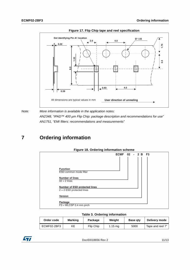
Figure 17. Flip Chip tape and reel specification
Note: More information is available in the application notes:AN2348, “IPAD™ 400 µm Flip Chip: package description and recommendations for use”AN1751, “EMI filters: recommendations and measurements”
7 Ordering information
Figure 18. Ordering information scheme
Dot identifying Pin A1 location
User direction of unreelingAll dimensions are typical values in mm
4.0
4.0
2.0
8.0
1.75
3.5
Ø 1.55
0.59
0.93
0.22
1.33
ST ST STxxzyww
xxzyww
xxzyww
Table 3. Ordering information
Order code Marking Package Weight Base qty Delivery mode
ECMF02-2BF3 KE Flip Chip 1.15 mg 5000 Tape and reel 7”
ECMF 02 - 2 B F3
Function
Number of lines
Number of ESD protected lines
Version
Package
ESD common mode filter
02 = 2 lines
2 = 2 ESD protected lines
F3 = WLCSP 0.4 mm pirch
Revision history ECMF02-2BF3
12/13 DocID018656 Rev 2
8 Revision history
Table 4. Document revision history
Date Revision Changes
09-Feb-2012 1 Initial release.
07-Mar-2014 2 Updated Figure 13.

DocID018656 Rev 2 13/13
ECMF02-2BF3
13
Please Read Carefully:
Information in this document is provided solely in connection with ST products. STMicroelectronics NV and its subsidiaries (“ST”) reserve theright to make changes, corrections, modifications or improvements, to this document, and the products and services described herein at anytime, without notice.
All ST products are sold pursuant to ST’s terms and conditions of sale.
Purchasers are solely responsible for the choice, selection and use of the ST products and services described herein, and ST assumes noliability whatsoever relating to the choice, selection or use of the ST products and services described herein.
No license, express or implied, by estoppel or otherwise, to any intellectual property rights is granted under this document. If any part of thisdocument refers to any third party products or services it shall not be deemed a license grant by ST for the use of such third party productsor services, or any intellectual property contained therein or considered as a warranty covering the use in any manner whatsoever of suchthird party products or services or any intellectual property contained therein.
UNLESS OTHERWISE SET FORTH IN ST’S TERMS AND CONDITIONS OF SALE ST DISCLAIMS ANY EXPRESS OR IMPLIEDWARRANTY WITH RESPECT TO THE USE AND/OR SALE OF ST PRODUCTS INCLUDING WITHOUT LIMITATION IMPLIEDWARRANTIES OF MERCHANTABILITY, FITNESS FOR A PARTICULAR PURPOSE (AND THEIR EQUIVALENTS UNDER THE LAWSOF ANY JURISDICTION), OR INFRINGEMENT OF ANY PATENT, COPYRIGHT OR OTHER INTELLECTUAL PROPERTY RIGHT.
ST PRODUCTS ARE NOT DESIGNED OR AUTHORIZED FOR USE IN: (A) SAFETY CRITICAL APPLICATIONS SUCH AS LIFESUPPORTING, ACTIVE IMPLANTED DEVICES OR SYSTEMS WITH PRODUCT FUNCTIONAL SAFETY REQUIREMENTS; (B)AERONAUTIC APPLICATIONS; (C) AUTOMOTIVE APPLICATIONS OR ENVIRONMENTS, AND/OR (D) AEROSPACE APPLICATIONSOR ENVIRONMENTS. WHERE ST PRODUCTS ARE NOT DESIGNED FOR SUCH USE, THE PURCHASER SHALL USE PRODUCTS ATPURCHASER’S SOLE RISK, EVEN IF ST HAS BEEN INFORMED IN WRITING OF SUCH USAGE, UNLESS A PRODUCT ISEXPRESSLY DESIGNATED BY ST AS BEING INTENDED FOR “AUTOMOTIVE, AUTOMOTIVE SAFETY OR MEDICAL” INDUSTRYDOMAINS ACCORDING TO ST PRODUCT DESIGN SPECIFICATIONS. PRODUCTS FORMALLY ESCC, QML OR JAN QUALIFIED AREDEEMED SUITABLE FOR USE IN AEROSPACE BY THE CORRESPONDING GOVERNMENTAL AGENCY.
Resale of ST products with provisions different from the statements and/or technical features set forth in this document shall immediately voidany warranty granted by ST for the ST product or service described herein and shall not create or extend in any manner whatsoever, anyliability of ST.
ST and the ST logo are trademarks or registered trademarks of ST in various countries.Information in this document supersedes and replaces all information previously supplied.
The ST logo is a registered trademark of STMicroelectronics. All other names are the property of their respective owners.
© 2014 STMicroelectronics - All rights reserved
STMicroelectronics group of companies
Australia - Belgium - Brazil - Canada - China - Czech Republic - Finland - France - Germany - Hong Kong - India - Israel - Italy - Japan - Malaysia - Malta - Morocco - Philippines - Singapore - Spain - Sweden - Switzerland - United Kingdom - United States of America
www.st.com