Dual high side smart power solid state relay€¦ · Dual high side smart power solid state relay...
22
This is information on a product in full production. November 2017 DocID15187 Rev 9 1/22 VNI2140 Dual high side smart power solid state relay Datasheet - production data Features Nominal current: 0.5 A per channel Shorted-load protections Junction overtemperature protection Case overtemperature protection for thermal independence of the channels Thermal case shutdown restart not simultaneous for the various channels Protection against loss of ground Current limitation 1 A per channel Undervoltage shutdown Open-load in off-state and short to V CC detection Open-drain diagnostic outputs 3.3 V CMOS/TTL compatible inputs Fast demagnetization of inductive loads Conforms to IEC 61131-2 Description The VNI2140J is a monolithic device designed using STMicroelectronics' VIPower technology. The device drives two independent resistive or inductive loads with one side connected to ground. Active current limitation prevents a drop in system power supply in cases of shorted-load, and built-in thermal shutdown protects the chip from damage due to overtemperature and short- circuit. In overload conditions, channel turns OFF and ON automatically to maintain the junction temperature between TTSD and TR. If the case temperature reaches TCSD, the overloaded channel is turned OFF and restarts only when case temperature decreases down to TCR. In order to avoid high-peak current from the supply, when more than one channel is overloaded the TCSD restart is not simultaneous. Non overloaded channels continue to operate normally. The open-drain diagnostics output indicates overtemperature conditions and open- load in off state. PowerSSO-12™ Table 1. Device summary Order codes Package Packaging VNI2140J PowerSSO-12™ Tube VNI2140JTR Tape and reel Table 2. Main features Type V demag (1) 1. Per channel. R DSon (1) I out (1) V CC VNI2140J V CC -45 V 0.08 1 A (2) 2. Current limitation. 45 V www.st.com
Transcript of Dual high side smart power solid state relay€¦ · Dual high side smart power solid state relay...

This is information on a product in full production.
November 2017 DocID15187 Rev 9 1/22
VNI2140
Dual high side smart power solid state relay
Datasheet - production data
Features
Nominal current: 0.5 A per channel
Shorted-load protections
Junction overtemperature protection
Case overtemperature protection for thermal independence of the channels
Thermal case shutdown restart not simultaneous for the various channels
Protection against loss of ground
Current limitation 1 A per channel
Undervoltage shutdown
Open-load in off-state and short to VCC detection
Open-drain diagnostic outputs
3.3 V CMOS/TTL compatible inputs
Fast demagnetization of inductive loads
Conforms to IEC 61131-2
Description
The VNI2140J is a monolithic device designed using STMicroelectronics' VIPower technology. The device drives two independent resistive or inductive loads with one side connected to ground. Active current limitation prevents a drop in system power supply in cases of shorted-load, and built-in thermal shutdown protects the chip from damage due to overtemperature and short-circuit. In overload conditions, channel turns OFF and ON automatically to maintain the junction temperature between TTSD and TR. If the case temperature reaches TCSD, the overloaded channel is turned OFF and restarts only when case temperature decreases down to TCR. In order to avoid high-peak current from the supply, when more than one channel is overloaded the TCSD restart is not simultaneous. Non overloaded channels continue to operate normally. The open-drain diagnostics output indicates overtemperature conditions and open-load in off state.
PowerSSO-12™
Table 1. Device summary
Order codes Package Packaging
VNI2140JPowerSSO-12™
Tube
VNI2140JTR Tape and reel
Table 2. Main features
Type Vdemag(1)
1. Per channel.
RDSon(1) Iout
(1) VCC
VNI2140J VCC -45 V 0.08 1 A(2)
2. Current limitation.
45 V
www.st.com
Contents VNI2140
2/22 DocID15187 Rev 9
Contents
1 Block diagram . . . . . . . . . . . . . . . . . . . . . . . . . . . . . . . . . . . . . . . . . . . . . . 3
2 Pin connections . . . . . . . . . . . . . . . . . . . . . . . . . . . . . . . . . . . . . . . . . . . . . 4
3 Maximum ratings . . . . . . . . . . . . . . . . . . . . . . . . . . . . . . . . . . . . . . . . . . . . 5
Thermal data. . . . . . . . . . . . . . . . . . . . . . . . . . . . . . . . . . . . . . . . . . . . . . . . . . . . . . 5
4 Electrical characteristics . . . . . . . . . . . . . . . . . . . . . . . . . . . . . . . . . . . . . 6
5 Truth table . . . . . . . . . . . . . . . . . . . . . . . . . . . . . . . . . . . . . . . . . . . . . . . . . 9
6 Switching waveforms . . . . . . . . . . . . . . . . . . . . . . . . . . . . . . . . . . . . . . . 10
7 Open-load . . . . . . . . . . . . . . . . . . . . . . . . . . . . . . . . . . . . . . . . . . . . . . . . . 13
8 Package and PCB thermal data . . . . . . . . . . . . . . . . . . . . . . . . . . . . . . . 15
9 Reverse polarity protection . . . . . . . . . . . . . . . . . . . . . . . . . . . . . . . . . . 17
10 Package information . . . . . . . . . . . . . . . . . . . . . . . . . . . . . . . . . . . . . . . . 18
10.1 PowerSSO-12 package information . . . . . . . . . . . . . . . . . . . . . . . . . . . . . 18
11 Revision history . . . . . . . . . . . . . . . . . . . . . . . . . . . . . . . . . . . . . . . . . . . 21

DocID15187 Rev 9 3/22
VNI2140 Block diagram
22
1 Block diagram
Figure 1. Block diagram

Pin connections VNI2140
4/22 DocID15187 Rev 9
2 Pin connections
Figure 2. Pin connections (top view)
Table 3. Pin description
No. Name Description
1 NC Not connected
2 Input 1 Channel 1 input 3.3 V CMOS/TTL compatible
3 Diag 1 Channel 1 diagnostic in open-drain configuration
4 GND Device ground connection
5 Diag 2 Channel 2 diagnostic in open-drain configuration
6 Input 2 Channel 2 input 3.3 V CMOS/TTL compatible
7 VCC Supply voltage
8 Output 2 Channel 2 power stage output, internally protected
9 Output 2 Channel 2 power stage output, internally protected
10 Output 1 Channel 1 power stage output, internally protected
11 Output 1 Channel 1 power stage output, internally protected
12 VCC Supply voltage
TAB TAB Supply voltage
VCCOutput 1Output 1
Output 2Output 2
VCC
NC
Input 1Diag 1
GNDDiag 2
Input 2

DocID15187 Rev 9 5/22
VNI2140 Maximum ratings
22
3 Maximum ratings
Thermal data
Table 4. Absolute maximum ratings
Symbol Parameter Value Unit
VCC Power supply voltage 45 V
-VCC Reverse supply voltage -0.3 V
IGND DC ground reverse current -250 mA
IOUT Output current (continuous) Internally limited A
IR Reverse output current (per channel) -5 A
IIN Input current (per channel) ± 10 mA
VIN Input voltage +VCC V
VDIAG Diag pin voltage +VCC V
IDIAG Diag pin current ± 10 mA
VESD Electrostatic discharge (R = 1.5 k; C = 100 pF) 2000 V
EASSingle pulse avalanche energy per channel, all channels driven simultaneously at Tamb = 125 °C, IOUT = 1 A
300 mJ
PTOT Power dissipation at Tc = 25 °C Internally limited W
TJ Junction operating temperature Internally limited C
TSTG Storage temperature -55 to 150 C
Table 5. Thermal data
Symbol Parameter Value Unit
Rth(JC) Thermal resistance junction to case(1)
1. Per channel.
Max. 1 °C/W
Rth(JA) Thermal resistance junction to ambient(2)
2. When mounted using minimum recommended pad size on FR-4 board.
Max.See Figure 11 on
page 15°C/W
Electrical characteristics VNI2140
6/22 DocID15187 Rev 9
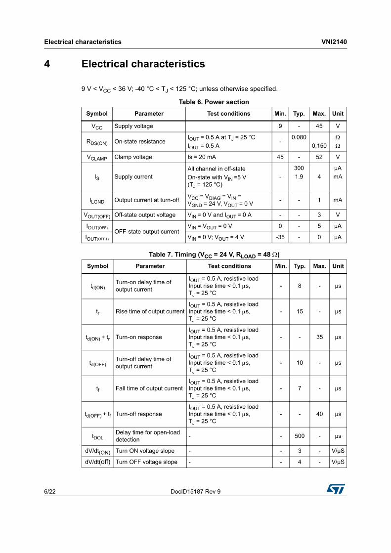
4 Electrical characteristics
9 V < VCC < 36 V; -40 °C < TJ < 125 °C; unless otherwise specified.
Table 6. Power section
Symbol Parameter Test conditions Min. Typ. Max. Unit
VCC Supply voltage 9 - 45 V
RDS(ON) On-state resistanceIOUT = 0.5 A at TJ = 25 °C
IOUT = 0.5 A-
0.080
0.150
VCLAMP Clamp voltage Is = 20 mA 45 - 52 V
IS Supply currentAll channel in off-state
On-state with VIN =5 V (TJ = 125 °C)
-
300
1.9 4
µA
mA
ILGND Output current at turn-offVCC = VDIAG = VIN = VGND = 24 V, VOUT = 0 V
- - 1 mA
VOUT(OFF) Off-state output voltage VIN = 0 V and IOUT = 0 A - - 3 V
IOUT(OFF)OFF-state output current
VIN = VOUT = 0 V 0 - 5 µA
IOUT(OFF1) VIN = 0 V; VOUT = 4 V -35 - 0 µA
Table 7. Timing (VCC = 24 V, RLOAD = 48 )
Symbol Parameter Test conditions Min. Typ. Max. Unit
td(ON)Turn-on delay time of output current
IOUT = 0.5 A, resistive load Input rise time < 0.1 s, TJ = 25 °C
- 8 - µs
tr Rise time of output currentIOUT = 0.5 A, resistive load Input rise time < 0.1 s, TJ = 25 °C
- 15 - µs
td(ON) + tr Turn-on responseIOUT = 0.5 A, resistive load Input rise time < 0.1 s, TJ = 25 °C
- - 35 µs
td(OFF)Turn-off delay time of output current
IOUT = 0.5 A, resistive load Input rise time < 0.1 s, TJ = 25 °C
- 10 - µs
tf Fall time of output currentIOUT = 0.5 A, resistive load Input rise time < 0.1 s, TJ = 25 °C
- 7 - µs
td(OFF) + tf Turn-off responseIOUT = 0.5 A, resistive load Input rise time < 0.1 s, TJ = 25 °C
- - 40 µs
tDOLDelay time for open-load detection
- - 500 - µs
dV/dt(ON) Turn ON voltage slope - - 3 - V/µS
dV/dt(off) Turn OFF voltage slope - - 4 - V/µS

DocID15187 Rev 9 7/22
VNI2140 Electrical characteristics
22
Table 8. Logical input
Symbol Parameter Test conditions Min. Typ. Max. Unit
VIL Input low level voltage - - - 0.8 V
VIH Input high level voltage - 2.20 - - V
VI(HYST)Input hysteresis voltage
- - 0.15 - V
IIN Input currentVIN = 15 V - - 10
AVIN = 36 V - - 210
Table 9. Protection and diagnostic
Symbol Parameter Test conditions Min. Typ. Max. Unit
VDIAG (1)
1. Diag determination > 100 ms after the switching edge.
Diag voltage output low
IDIAG = 1.5 mA (fault condition) - - 0.6 V
VUSDUndervoltage protection
- 7 - 9 V
VUSDHYSUndervoltage hysteresis
- 0.4 0.5 - V
ILIMDC short-circuit current
VCC = 24 V; RLOAD < 10 m 1 - 2 A
ILDIAG Diag leakage current VCC = 32 V - 30 - A
VOL
Open-load off-state voltage detection threshold
VIN = 0 V 2 3 4 V
TTSDJunction shutdown temperature
- 150 170 - °C
TRJunction reset temperature
- 135 155 200 °C
THISTJunction thermal hysteresis
- 7 15 - °C
TCSDCase shutdown temperature
- 125 130 135 °C
TCRCase reset temperature
- 110 - - °C
TCHYSTCase thermal hysteresis
- 7 15 - °C
VdemagOutput voltage at turn-OFF
IOUT = 0.5 A; LLOAD >= 1 mHVCC-45
VCC-50
VCC-52
V

Electrical characteristics VNI2140
8/22 DocID15187 Rev 9
Figure 3. Current and voltage conventions

DocID15187 Rev 9 9/22
VNI2140 Truth table
22
5 Truth table
.
Table 10. Truth table
IC condition INPUTn OUTPUTn DIAGn
Normal operationL
H
L
H
H
H
OvertemperatureL
H
L
L
H
L
UndervoltageL
H
L
L
X
X
Shorted-load
(current limitation)
L
H
L
X
H
H
Output voltage > VOLL
H
Z(1)
H
1. Z = depending on the external circuit.
L
H
Short to VCCL
H
H
H
L
H
Switching waveforms VNI2140
10/22 DocID15187 Rev 9
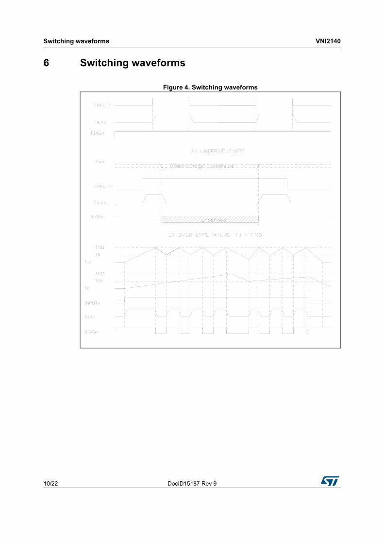
6 Switching waveforms
Figure 4. Switching waveforms

DocID15187 Rev 9 11/22
VNI2140 Switching waveforms
22
Figure 5. Switching waveforms (continued)
Figure 6. Switching parameter test conditions
IOUT
VIN

Switching waveforms VNI2140
12/22 DocID15187 Rev 9
Figure 7. Typical application circuit
DocID15187 Rev 9 13/22
VNI2140 Open-load
22
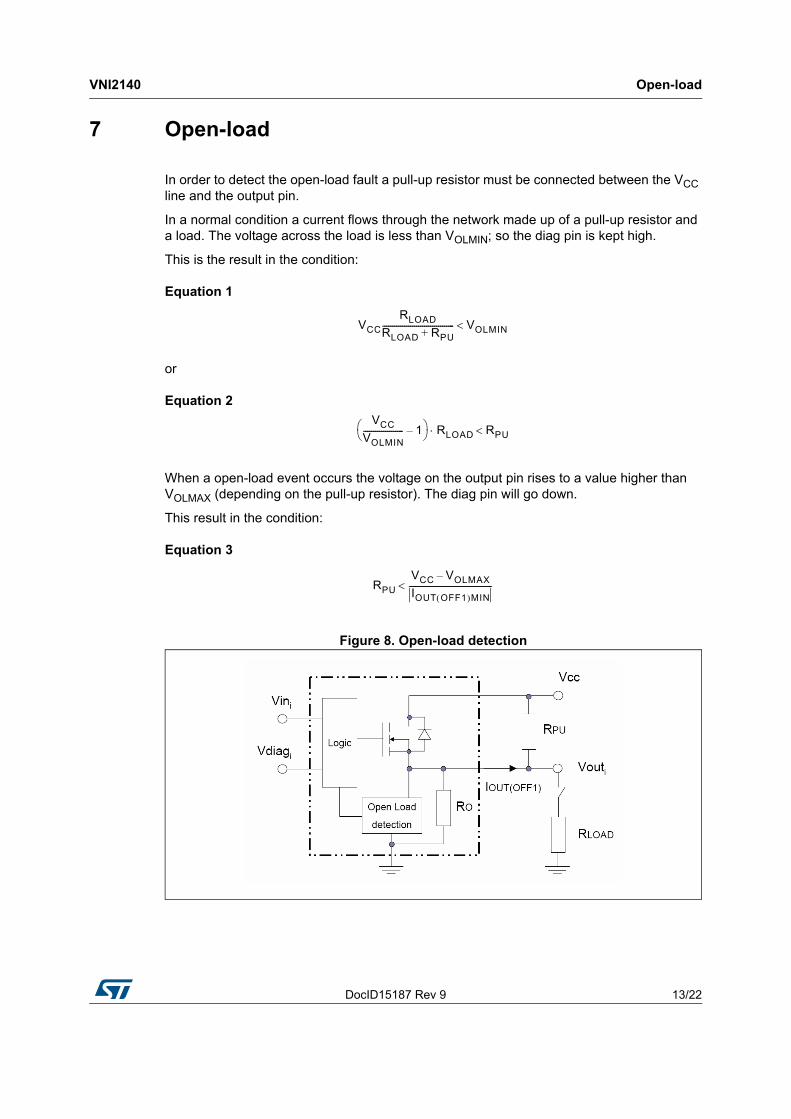
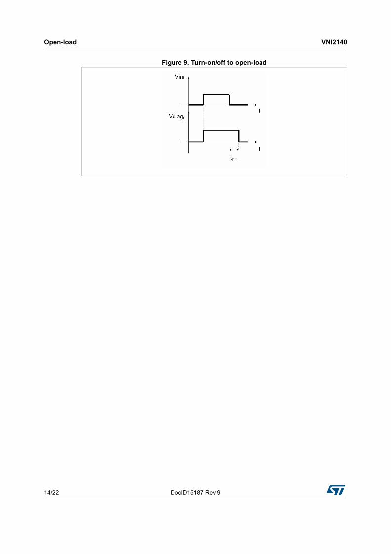
7 Open-load
In order to detect the open-load fault a pull-up resistor must be connected between the VCC line and the output pin.
In a normal condition a current flows through the network made up of a pull-up resistor and a load. The voltage across the load is less than VOLMIN; so the diag pin is kept high.
This is the result in the condition:
Equation 1
or
Equation 2
When a open-load event occurs the voltage on the output pin rises to a value higher than VOLMAX (depending on the pull-up resistor). The diag pin will go down.
This result in the condition:
Equation 3
Figure 8. Open-load detection
VCC
RLOAD
RLOAD RPU+------------------------------------ VOLMIN
VCC
VOLMIN-------------------- 1– RLOAD RPU
RPU
VCC VOLMAX–
IOUT OFF1 MIN------------------------------------------
Open-load VNI2140
14/22 DocID15187 Rev 9
Figure 9. Turn-on/off to open-load
DocID15187 Rev 9 15/22
VNI2140 Package and PCB thermal data
22
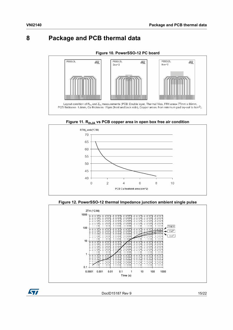
8 Package and PCB thermal data
Figure 10. PowerSSO-12 PC board
Figure 11. RthJA vs PCB copper area in open box free air condition
Figure 12. PowerSSO-12 thermal Impedance junction ambient single pulse
Package and PCB thermal data VNI2140
16/22 DocID15187 Rev 9
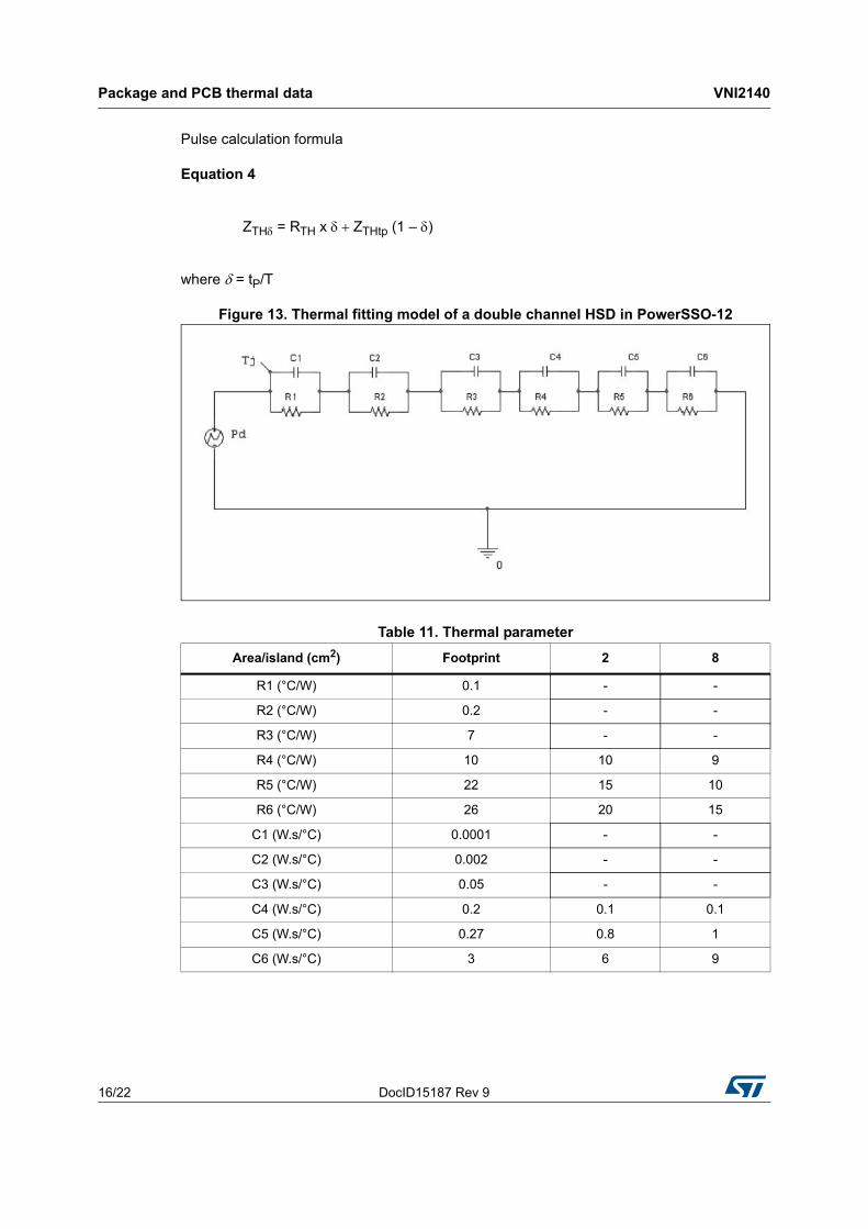
Pulse calculation formula
Equation 4
ZTH = RTH x ZTHtp (1 – )
where = tP/T
Figure 13. Thermal fitting model of a double channel HSD in PowerSSO-12
Table 11. Thermal parameter
Area/island (cm2) Footprint 2 8
R1 (°C/W) 0.1 - -
R2 (°C/W) 0.2 - -
R3 (°C/W) 7 - -
R4 (°C/W) 10 10 9
R5 (°C/W) 22 15 10
R6 (°C/W) 26 20 15
C1 (W.s/°C) 0.0001 - -
C2 (W.s/°C) 0.002 - -
C3 (W.s/°C) 0.05 - -
C4 (W.s/°C) 0.2 0.1 0.1
C5 (W.s/°C) 0.27 0.8 1
C6 (W.s/°C) 3 6 9
DocID15187 Rev 9 17/22
VNI2140 Reverse polarity protection
22
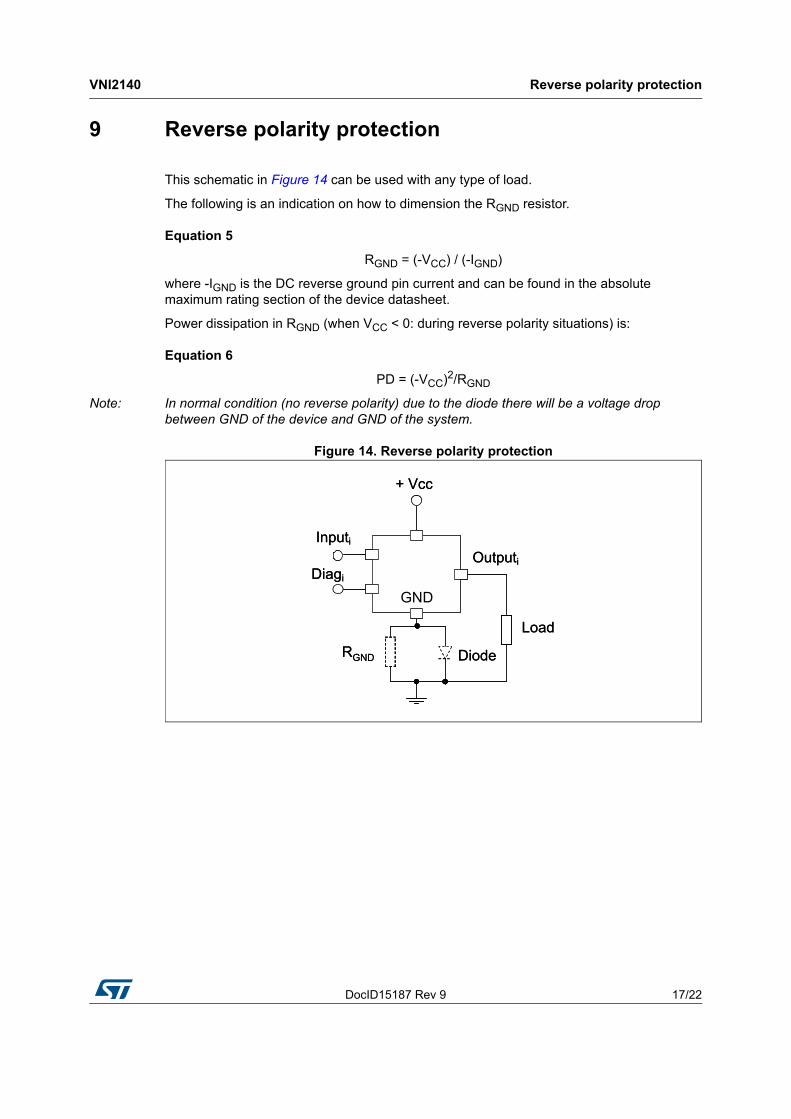
9 Reverse polarity protection
This schematic in Figure 14 can be used with any type of load.
The following is an indication on how to dimension the RGND resistor.
Equation 5
RGND = (-VCC) / (-IGND)
where -IGND is the DC reverse ground pin current and can be found in the absolute maximum rating section of the device datasheet.
Power dissipation in RGND (when VCC < 0: during reverse polarity situations) is:
Equation 6
PD = (-VCC)2/RGND
Note: In normal condition (no reverse polarity) due to the diode there will be a voltage drop between GND of the device and GND of the system.
Figure 14. Reverse polarity protection
Diagi
Inputi
GND
Outputi
+ Vcc
RGND
Load
Diode
Diagi
Inputi
GND
Outputi
+ Vcc
RGND
Load
Diode
Package information VNI2140
18/22 DocID15187 Rev 9
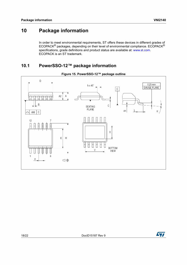
10 Package information
In order to meet environmental requirements, ST offers these devices in different grades of ECOPACK® packages, depending on their level of environmental compliance. ECOPACK® specifications, grade definitions and product status are available at: www.st.com. ECOPACK is an ST trademark.
10.1 PowerSSO-12™ package information
Figure 15. PowerSSO-12™ package outline
DocID15187 Rev 9 19/22
VNI2140 Package information
22
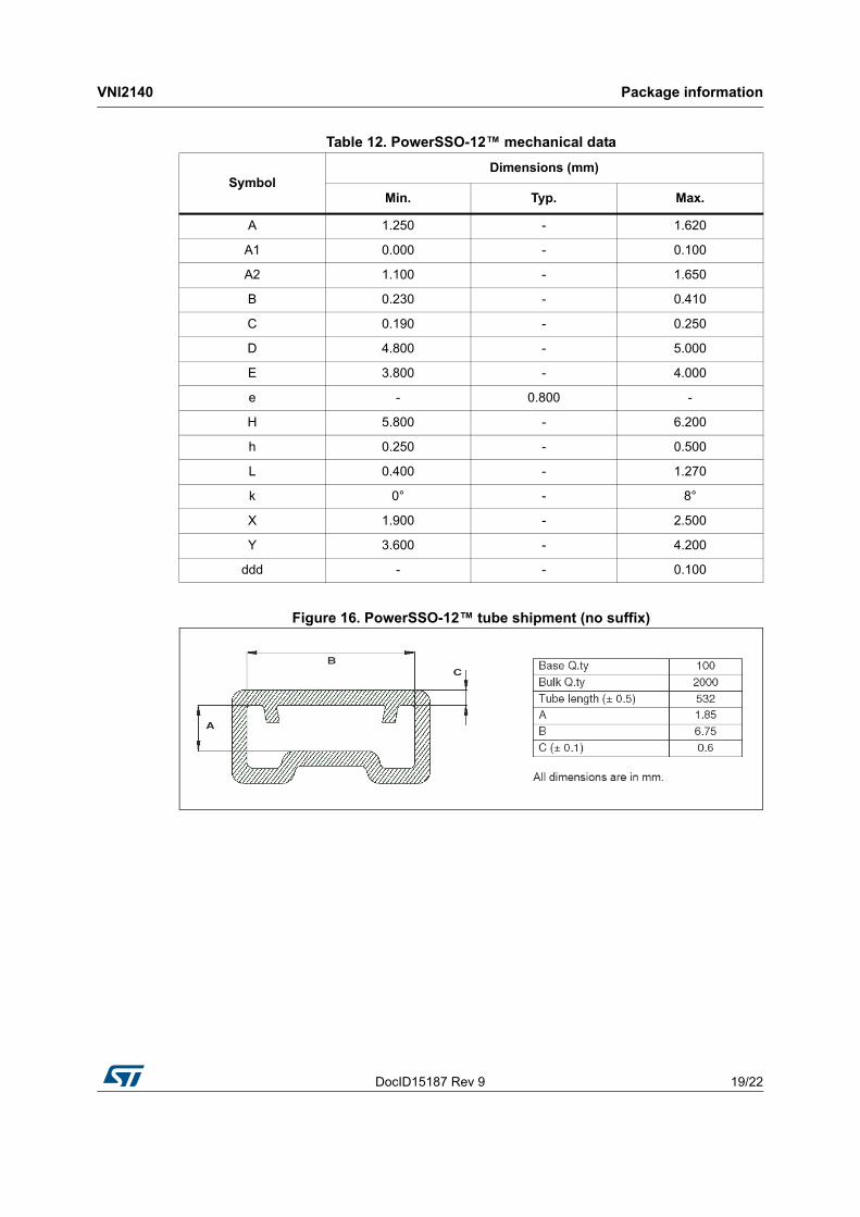
Figure 16. PowerSSO-12™ tube shipment (no suffix)
Table 12. PowerSSO-12™ mechanical data
Symbol Dimensions (mm)
Min. Typ. Max.
A 1.250 - 1.620
A1 0.000 - 0.100
A2 1.100 - 1.650
B 0.230 - 0.410
C 0.190 - 0.250
D 4.800 - 5.000
E 3.800 - 4.000
e - 0.800 -
H 5.800 - 6.200
h 0.250 - 0.500
L 0.400 - 1.270
k 0° - 8°
X 1.900 - 2.500
Y 3.600 - 4.200
ddd - - 0.100
Package information VNI2140
20/22 DocID15187 Rev 9
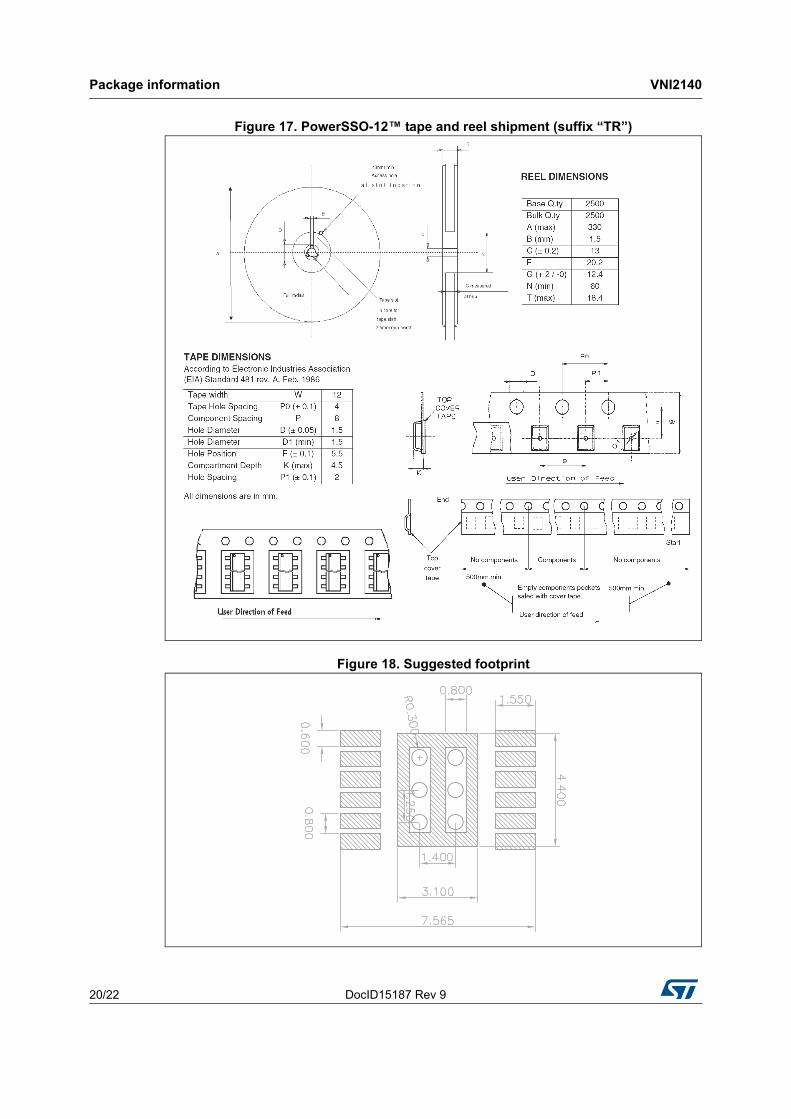
Figure 17. PowerSSO-12™ tape and reel shipment (suffix “TR”)
Figure 18. Suggested footprint
DocID15187 Rev 9 21/22
VNI2140 Revision history
22
11 Revision history
Table 13. Document revision history
Date Revision Changes
16-Dec-2008 1 Initial release
29-Apr-2009 2 Updated Table 5 on page 6
03-Jul-2009 3 Updated features in coverpage and Table 5 on page 6
27-Aug-2009 4 Updated Section 9: Reverse polarity protection
25-Mar-2010 5 Updated Coverpage and Table 4 on page 5
26-Apr-2010 6 Updated Table 5 on page 6
21-Jul-2010 7 Updated Table 8 on page 7
15-Nov-2011 8 Updated Figure 18 on page 21
09-Nov-2017 9Updated Table 4 on page 5 and Table 7 on page 6.
Minor modifications throughout document.

VNI2140
22/22 DocID15187 Rev 9
IMPORTANT NOTICE – PLEASE READ CAREFULLY
STMicroelectronics NV and its subsidiaries (“ST”) reserve the right to make changes, corrections, enhancements, modifications, and improvements to ST products and/or to this document at any time without notice. Purchasers should obtain the latest relevant information on ST products before placing orders. ST products are sold pursuant to ST’s terms and conditions of sale in place at the time of order acknowledgement.
Purchasers are solely responsible for the choice, selection, and use of ST products and ST assumes no liability for application assistance or the design of Purchasers’ products.
No license, express or implied, to any intellectual property right is granted by ST herein.
Resale of ST products with provisions different from the information set forth herein shall void any warranty granted by ST for such product.
ST and the ST logo are trademarks of ST. All other product or service names are the property of their respective owners.
Information in this document supersedes and replaces information previously supplied in any prior versions of this document.
© 2017 STMicroelectronics – All rights reserved