Dual 3 MHz, 1200 mA Buck Regulators with One 300 mA LDO ... · 3 MHz buck operation with forced PWM...
28
Dual 3 MHz, 1200 mA Buck Regulators with One 300 mA LDO Data Sheet ADP5024 Rev. E Document Feedback Information furnished by Analog Devices is believed to be accurate and reliable. However, no responsibility isassumed byAnalog Devicesfor its use, nor foranyinfringements of patents or other rights ofthird partiesthat mayresult from its use.Specifications subjectto change without notice.No license is granted by implication or otherwise under any patent or patent rights of Analog Devices. Trademarks and registered trademarks arethe property of their respectiveowners. One Technology Way, P.O. Box 9106, Norwood, MA 02062-9106, U.S.A. Tel: 781.329.4700 ©2011–2013 Analog Devices, Inc. All rights reserved. Technical Support www.analog.com FEATURES Main input voltage range: 2.3 V to 5.5 V Two 1200 mA buck regulators and one 300 mA LDO 24-lead, 4 mm × 4 mm LFCSP package Regulator accuracy: ±1.8% Factory programmable or external adjustable VOUTx 3 MHz buck operation with forced PWM and automatic PWM/PSM modes BUCK1/BUCK2: output voltage range from 0.8 V to 3.8 V LDO: output voltage range from 0.8 V to 5.2 V LDO: input supply voltage from 1.7 V to 5.5 V LDO: high PSRR and low output noise APPLICATIONS Power for processors, ASICS, FPGAs, and RF chipsets Portable instrumentation and medical devices Space constrained devices GENERAL DESCRIPTION The ADP5024 combines two high performance buck regula- tors and one low dropout (LDO) regulator in a small, 24-lead, 4 mm × 4 mm LFCSP to meet demanding performance and board space requirements. The high switching frequency of the buck regulators enables tiny multilayer external components and minimizes the board space. When the MODE pin is set high, the buck regulators operate in forced PWM mode. When the MODE pin is set low, the buck regulators operate in PWM mode when the load current is above a predefined threshold. When the load current falls below a pre- defined threshold, the regulator operates in power save mode (PSM), improving the light load efficiency. Table 1. Family Models Model Channels Maximum Current Package ADP5023 2 Buck, 1 LDO 800 mA, 300 mA LFCSP (CP-24-10) ADP5024 2 Buck, 1 LDO 1.2 A, 300 mA LFCSP (CP-24-10) ADP5034 2 Buck, 2 LDOs 1.2 A, 300 mA LFCSP (CP-24-10), TSSOP (RE-28-1) ADP5037 2 Buck, 2 LDOs 800 mA, 300 mA LFCSP (CP-24-10) ADP5033 2 Buck, 2 LDOs with 2 EN pins 800 mA, 300 mA WLCSP (CB-16-8) The two bucks operate out of phase to reduce the input capacitor requirement. The low quiescent current, low dropout voltage, and wide input voltage range of the LDO extends the battery life of portable devices. The ADP5024 LDO maintains power supply rejection greater than 60 dB for frequencies as high as 10 kHz while operating with a low headroom voltage. Regulators in the ADP5024 are activated though dedicated enable pins. The default output voltages can be either externally set in the adjustable version or factory programmable to a wide range of preset values in the fixed voltage version. TYPICAL APPLICATION CIRCUIT VIN1 VIN3 EN1 PWM PSM/PWM 2.3V TO 5.5V SW1 FB1 R2 R1 VOUT1 PGND1 MODE C5 10μF V OUT1 AT 1200mA V OUT2 AT 1200mA V OUT3 AT 300mA L1 1μH EN1 BUCK1 MODE C3 1μF C2 4.7μF C1 4.7μF AVIN C AVIN 0.1μF VIN2 EN2 AGND EN2 BUCK2 MODE EN3 1.7V TO 5.5V ON OFF ON OFF EN3 LDO (ANALOG) HOUSEKEEPING SW2 FB2 R4 R3 VOUT2 PGND2 C6 10μF L2 1μH FB3 R6 R5 VOUT3 C7 1μF ADP5024 09888-001 Figure 1.
Transcript of Dual 3 MHz, 1200 mA Buck Regulators with One 300 mA LDO ... · 3 MHz buck operation with forced PWM...

Dual 3 MHz, 1200 mA Buck Regulators with One 300 mA LDO
Data Sheet ADP5024
Rev. E Document Feedback Information furnished by Analog Devices is believed to be accurate and reliable. However, no responsibility is assumed by Analog Devices for its use, nor for any infringements of patents or other rights of third parties that may result from its use. Specifications subject to change without notice. No license is granted by implication or otherwise under any patent or patent rights of Analog Devices. Trademarks and registered trademarks are the property of their respective owners.
One Technology Way, P.O. Box 9106, Norwood, MA 02062-9106, U.S.A. Tel: 781.329.4700 ©2011–2013 Analog Devices, Inc. All rights reserved. Technical Support www.analog.com
FEATURES Main input voltage range: 2.3 V to 5.5 V Two 1200 mA buck regulators and one 300 mA LDO 24-lead, 4 mm × 4 mm LFCSP package Regulator accuracy: ±1.8% Factory programmable or external adjustable VOUTx 3 MHz buck operation with forced PWM and automatic
PWM/PSM modes BUCK1/BUCK2: output voltage range from 0.8 V to 3.8 V LDO: output voltage range from 0.8 V to 5.2 V LDO: input supply voltage from 1.7 V to 5.5 V LDO: high PSRR and low output noise
APPLICATIONS Power for processors, ASICS, FPGAs, and RF chipsets Portable instrumentation and medical devices Space constrained devices
GENERAL DESCRIPTION The ADP5024 combines two high performance buck regula-tors and one low dropout (LDO) regulator in a small, 24-lead, 4 mm × 4 mm LFCSP to meet demanding performance and board space requirements.
The high switching frequency of the buck regulators enables tiny multilayer external components and minimizes the board space. When the MODE pin is set high, the buck regulators operate in forced PWM mode. When the MODE pin is set low, the buck regulators operate in PWM mode when the load current is above
a predefined threshold. When the load current falls below a pre-defined threshold, the regulator operates in power save mode (PSM), improving the light load efficiency.
Table 1. Family Models
Model Channels Maximum Current Package
ADP5023 2 Buck, 1 LDO 800 mA, 300 mA
LFCSP (CP-24-10)
ADP5024 2 Buck, 1 LDO 1.2 A, 300 mA
LFCSP (CP-24-10)
ADP5034 2 Buck, 2 LDOs 1.2 A, 300 mA
LFCSP (CP-24-10), TSSOP (RE-28-1)
ADP5037 2 Buck, 2 LDOs 800 mA, 300 mA
LFCSP (CP-24-10)
ADP5033 2 Buck, 2 LDOs with 2 EN pins
800 mA, 300 mA
WLCSP (CB-16-8)
The two bucks operate out of phase to reduce the input capacitor requirement. The low quiescent current, low dropout voltage, and wide input voltage range of the LDO extends the battery life of portable devices. The ADP5024 LDO maintains power supply rejection greater than 60 dB for frequencies as high as 10 kHz while operating with a low headroom voltage.
Regulators in the ADP5024 are activated though dedicated enable pins. The default output voltages can be either externally set in the adjustable version or factory programmable to a wide range of preset values in the fixed voltage version.
TYPICAL APPLICATION CIRCUIT
VIN1
VIN3
EN1PWM
PSM/PWM
2.3V TO5.5V
SW1
FB1
R2
R1
VOUT1
PGND1
MODE
C510µF
VOUT1 AT1200mA
VOUT2 AT1200mA
VOUT3 AT300mA
L1 1µH
EN1
BUCK1
MODE
C31µF
C24.7µF
C14.7µF
AVINCAVIN0.1µF
VIN2
EN2
AGND
EN2
BUCK2
MODE
EN3
1.7V TO5.5V
ONOFF
ONOFF
EN3 LDO(ANALOG)
HOUSEKEEPING
SW2
FB2
R4
R3
VOUT2
PGND2C610µF
L2 1µH
FB3
R6
R5VOUT3
C71µF
ADP5024
0988
8-00
1
Figure 1.
ADP5024 Data Sheet
Rev. E | Page 2 of 28
TABLE OF CONTENTS Features .....................................................................................1 Applications...............................................................................1 General Description ..................................................................1 Typical Application Circuit........................................................1 Revision History ........................................................................2 Specifications .............................................................................3
General Specifications............................................................3 BUCK1 and BUCK2 Specifications........................................4 LDO Specifications ................................................................5 Input and Output Capacitor, Recommended Specifications ..6
Absolute Maximum Ratings ......................................................7 Thermal Resistance ................................................................7 ESD Caution ..........................................................................7
Pin Configuration and Function Descriptions...........................8 Typical Performance Characteristics .........................................9
Theory of Operation................................................................ 16 Power Management Unit ..................................................... 17 BUCK1 and BUCK2 ............................................................ 19 LDO..................................................................................... 20
Applications Information ........................................................ 21 Buck External Component Selection ................................... 21 LDO External Component Selection ................................... 23
Power Dissipation and Thermal Considerations ..................... 24 Buck Regulator Power Dissipation....................................... 24 Junction Temperature .......................................................... 25
PCB Layout Guidelines............................................................ 26 Typical Application Schematics ............................................... 27
Bill of Materials.................................................................... 27 Outline Dimensions ................................................................ 28
Ordering Guide ................................................................... 28
REVISION HISTORY 5/13—Rev. D to Rev. E
Added Table 1; Renumbered Sequentially .................................1 Changes to Figure 1 ...................................................................1 Changes to NC Pin Description.................................................8 Changes to Figure 48 ...............................................................20 Changes to Figure 50 ...............................................................22 Changes to Figure 52 and Figure 53.........................................27
1/13—Rev. C to Rev. D
Changes to Figure 9 .................................................................10 Changes to Ordering Guide .....................................................28
12/12—Rev. B to Rev. C
Changes to Ordering Guide .....................................................28
11/12—Rev. A to Rev. B
Changes to Features Section ......................................................1 Changes to Output Voltage Accuracy and Voltage Feedback Parameters, Table 2 ....................................................................4 Changes to Output Voltage Accuracy and Voltage Feedback Parameters, Table 3 ....................................................................5
Changes to Figure 6, Figure 7 and Figure 8................................ 9 Changes to Figure 30 and Figure 31 ........................................ 13 Changes to Figure 34 ............................................................... 14 Change to Figure 38 ................................................................ 14 Changes to Undervoltage Lockout Section .............................. 17 Changes to Buck Regulator Power Dissipation Section ........... 24
1/12—Rev. 0 to Rev. A
Changes to Features Section and Figure 1 ................................. 1 Changes to Table 2..................................................................... 4 Changes to Table 3..................................................................... 5 Changes to Table 4..................................................................... 6 Changes to Table 7..................................................................... 8 Changes to Figure 34 ............................................................... 14 Changes to LDO Section and Figure 48................................... 20 Changes to Table 9 and Figure 50 ............................................ 22 Changes to Buck Regulator Power Dissipation Section ........... 24 Changes to Figure 52 and Figure 53 ........................................ 27
8/11—Revision 0: Initial Version

Data Sheet ADP5024
Rev. E | Page 3 of 28
SPECIFICATIONS GENERAL SPECIFICATIONS VAVIN = VIN1 = VIN2 = 2.3 V to 5.5 V; VIN3 = 1.7 V to 5.5 V; TJ = −40°C to +125°C for minimum/maximum specifications, and TA = 25°C for typical specifications, unless otherwise noted.
Table 2. Parameter Symbol Test Conditions/Comments Min Typ Max Unit INPUT VOLTAGE RANGE VAVIN, VIN1, VIN2 2.3 5.5 V
THERMAL SHUTDOWN Threshold TSSD TJ rising 150 °C Hysteresis TSSD-HYS 20 °C
START-UP TIME1 BUCK1, LDO tSTART1 250 µs BUCK2 tSTART2 300 µs
EN1, EN2, EN3, MODE INPUTS Input Logic High VIH 1.1 V Input Logic Low VIL 0.4 V Input Leakage Current VI-LEAKAGE 0.05 1 µA
INPUT CURRENT All Channels Enabled ISTBY-NOSW No load, no buck switching 108 175 µA All Channels Disabled ISHUTDOWN TJ = −40°C to +85°C 0.3 1 µA
VIN1 UNDERVOLTAGE LOCKOUT High UVLO Input Voltage Rising UVLOVIN1RISE 3.9 V High UVLO Input Voltage Falling UVLOVIN1FALL 3.1 V Low UVLO Input Voltage Rising UVLOVIN1RISE 2.275 V Low UVLO Input Voltage Falling UVLOVIN1FALL 1.95 V
1 Start-up time is defined as the time from EN1 = EN2 = EN3 from 0 V to VAVIN to VOUT1, VOUT2, and VOUT3 reaching 90% of their nominal levels. Start-up times are
shorter for individual channels if another channel is already enabled. See the Typical Performance Characteristics section for more information.

ADP5024 Data Sheet
Rev. E | Page 4 of 28
BUCK1 AND BUCK2 SPECIFICATIONS VAVIN = VIN1 = VIN2 = 2.3 V to 5.5 V; TJ = −40°C to +125°C for minimum/maximum specifications, and TA = 25°C for typical specifications, unless otherwise noted. 1
Table 3. Parameter Symbol Test Conditions/Comments Min Typ Max Unit OUTPUT CHARACTERISTICS
Output Voltage Accuracy ΔVOUT1/VOUT1, ΔVOUT2/VOUT2
ILOAD1 = ILOAD2 = 0 mA −1.8 +1.8 %
Line Regulation (ΔVOUT1/VOUT1)/ΔVIN1, (ΔVOUT2/VOUT2)/ΔVIN2
PWM mode −0.05 %/V
Load Regulation (ΔVOUT1/VOUT1)/ΔIOUT1, (ΔVOUT2/VOUT2)/ΔIOUT2
ILOAD = 0 mA to 1200 mA, PWM mode −0.1 %/A
VOLTAGE FEEDBACK VFB1, VFB2 Models with adjustable outputs 0.491 0.5 0.509 V
OPERATING SUPPLY CURRENT MODE = ground BUCK1 Only IIN ILOAD1 = 0 mA, device not switching, all other
channels disabled 44 μA
BUCK2 Only IIN ILOAD2 = 0 mA, device not switching, all other channels disabled
55 μA
BUCK1 and BUCK2 IIN ILOAD1 = ILOAD2 = 0 mA, device not switching, LDO channels disabled
67 μA
PSM CURRENT THRESHOLD IPSM PSM to PWM operation 100 mA
SW CHARACTERISTICS SW On Resistance RNFET VIN1 = VIN2 = 3.6 V 155 240 mΩ RPFET VIN1 = VIN2 = 3.6 V 205 310 mΩ RNFET VIN1 = VIN2 = 5.5 V 137 204 mΩ RPFET VIN1 = VIN2 = 5.5 V 162 243 mΩ Current Limit ILIMIT1, ILIMIT2 PFET switch peak current limit 1600 1950 2300 mA
ACTIVE PULL-DOWN RPDWN-B Channel disabled 75 Ω OSCILLATOR FREQUENCY fSW 2.5 3.0 3.5 MHz 1 All limits at temperature extremes are guaranteed via correlation using standard statistical quality control (SQC).

Data Sheet ADP5024
Rev. E | Page 5 of 28
LDO SPECIFICATIONS VIN3 = (VOUT3 + 0.5 V) or 1.7 V (whichever is greater) to 5.5 V; CIN = COUT = 1 µF; TJ = −40°C to +125°C for minimum/maximum specifications, and TA = 25°C for typical specifications, unless otherwise noted. 1
Table 4. Parameter Symbol Test Conditions/Comments Min Typ Max Unit INPUT VOLTAGE RANGE VIN3 1.7 5.5 V OPERATING SUPPLY CURRENT
Bias Current per LDO2 IVIN3BIAS IOUT3 = 0 µA 10 30 µA IOUT3 = 10 mA 60 100 µA IOUT3 = 300 mA 165 245 µA
Total System Input Current IIN Includes all current into AVIN, VIN1, VIN2, and VIN3
LDO Only IOUT3 = 0 µA, all other channels disabled
53 µA
OUTPUT CHARACTERISTICS Output Voltage Accuracy ΔVOUT3/VOUT3 100 µA < IOUT3 < 300 mA −1.8 +1.8 % Line Regulation (ΔVOUT3/VOUT3)/ΔVIN3 IOUT3 = 1 mA −0.03 +0.03 %/V Load Regulation3 (ΔVOUT3/VOUT3)/ΔIOUT3 IOUT3 = 1 mA to 300 mA 0.001 0.003 %/mA
VOLTAGE FEEDBACK VFB3 0.491 0.5 0.509 V DROPOUT VOLTAGE4 VDROPOUT VOUT3 = 5.2 V, IOUT3 = 300 mA 50 mV VOUT3 = 3.3 V, IOUT3 = 300 mA 75 140 VOUT3 = 2.5 V, IOUT3 = 300 mA 100 mV VOUT3 = 1.8 V, IOUT3 = 300 mA 180 mV CURRENT-LIMIT THRESHOLD5 ILIMIT3 335 600 mA ACTIVE PULL-DOWN RPDWN-L Channel disabled 600 Ω OUTPUT NOISE
Regulator LDO NOISELDO 10 Hz to 100 kHz, VIN3 = 5 V, VOUT3 = 2.8 V 100 µV rms POWER SUPPLY REJECTION
RATIO PSRR
Regulator LDO 10 kHz, VIN3 = 3.3 V, VOUT3 = 2.8 V, IOUT3 = 1 mA
60 dB
100 kHz, VIN3 = 3.3 V, VOUT3 = 2.8 V, IOUT3 = 1 mA
62 dB
1 MHz, VIN3 = 3.3 V, VOUT3 = 2.8 V, IOUT3 = 1 mA
63 dB
1 All limits at temperature extremes are guaranteed via correlation using standard statistical quality control (SQC). 2 This is the input current into VIN3, which is not delivered to the output load. 3 Based on an endpoint calculation using 1 mA and 300 mA loads. 4 Dropout voltage is defined as the input-to-output voltage differential when the input voltage is set to the nominal output voltage. This applies only to output voltages
above 1.7 V. 5 Current-limit threshold is defined as the current at which the output voltage drops to 90% of the specified typical value. For example, the current limit for a 3.0 V
output voltage is defined as the current that causes the output voltage to drop to 90% of 3.0 V or 2.7 V.

ADP5024 Data Sheet
Rev. E | Page 6 of 28
INPUT AND OUTPUT CAPACITOR, RECOMMENDED SPECIFICATIONS TA = −40°C to +125°C, unless otherwise specified.
Table 5. Parameter Symbol Min Typ Max Unit NOMINAL INPUT AND OUTPUT CAPACITOR RATINGS
BUCK1, BUCK2 Input Capacitor Ratings CMIN1, CMIN2 4.7 40 µF BUCK1, BUCK2 Output Capacitor Ratings CMIN1, CMIN2 10 40 µF LDO1 Input and Output Capacitor Ratings CMIN3, CMIN4 1.0 µF
CAPACITOR ESR RESR 0.001 1 Ω 1 The minimum input and output capacitance should be greater than 0.70 µF over the full range of operating conditions. The full range of operating conditions in the
application must be considered during device selection to ensure that the minimum capacitance specification is met. X7R- and X5R-type capacitors are recommended; Y5V and Z5U capacitors are not recommended for use because of their poor temperature and dc bias characteristics.

Data Sheet ADP5024
Rev. E | Page 7 of 28
ABSOLUTE MAXIMUM RATINGS Table 6. Parameter Rating
AVIN to AGND −0.3 V to +6 V VIN1, VIN2 to AVIN −0.3 V to +0.3 V PGND1, PGND2 to AGND −0.3 V to +0.3 V VIN3, VOUT1, VOUT2, FB1, FB2, FB3,
EN1, EN2, EN3, MODE to AGND −0.3 V to (AVIN + 0.3 V)
VOUT3 to AGND −0.3 V to (VIN3 + 0.3 V) SW1 to PGND1 −0.3 V to (VIN1 + 0.3 V) SW2 to PGND2 −0.3 V to (VIN2 + 0.3 V) Storage Temperature Range −65°C to +150°C Operating Junction Temperature
Range −40°C to +125°C
Soldering Conditions JEDEC J-STD-020
Stresses above those listed under Absolute Maximum Ratings may cause permanent damage to the device. This is a stress rating only; functional operation of the device at these or any other conditions above those indicated in the operational section of this specification is not implied. Exposure to absolute maximum rating conditions for extended periods may affect device reliability.
For detailed information on power dissipation, see the Power Dissipation and Thermal Considerations section.
THERMAL RESISTANCE θJA is specified for the worst-case conditions, that is, a device soldered in a circuit board for surface-mount packages.
Table 7. Thermal Resistance Package Type θJA θJC Unit 24-Lead, 0.5 mm pitch LFCSP 35 3 °C/W
ESD CAUTION
ADP5024 Data Sheet
Rev. E | Page 8 of 28
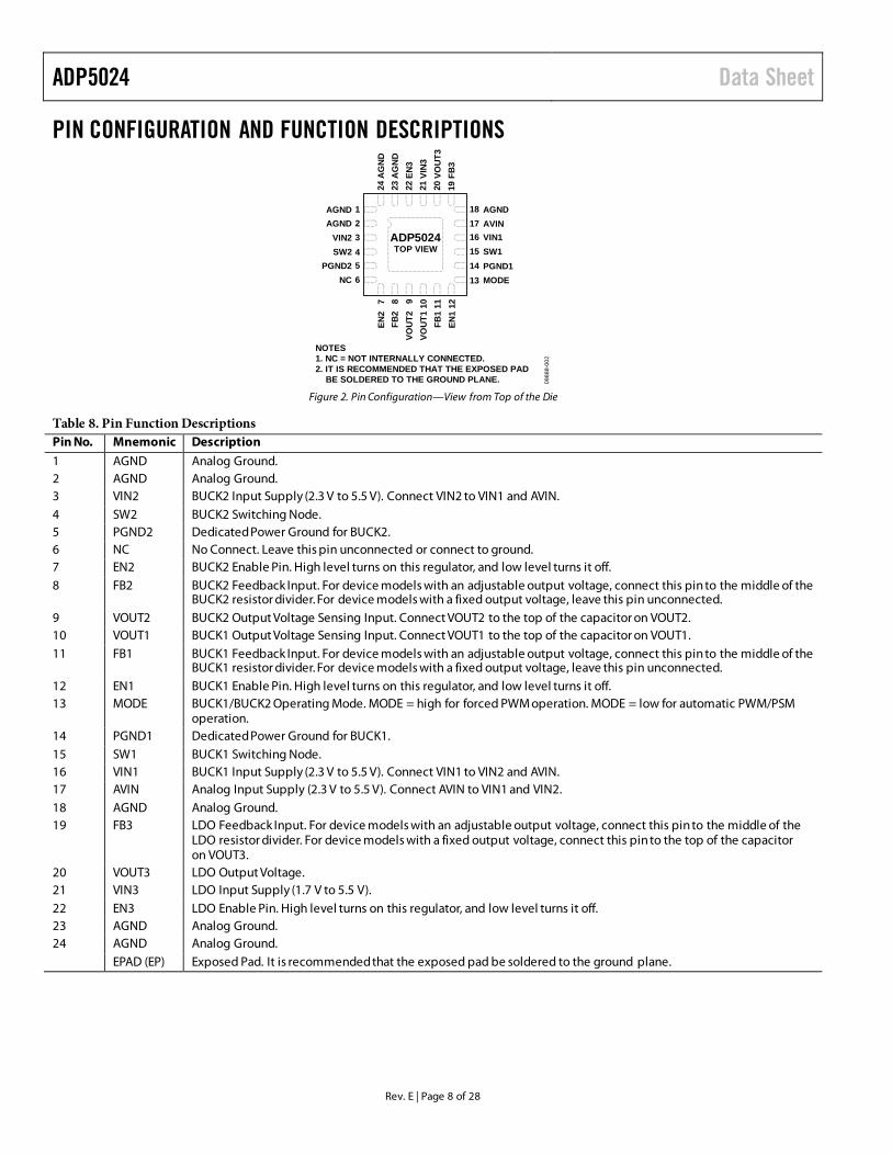
PIN CONFIGURATION AND FUNCTION DESCRIPTIONS
NOTES1. NC = NOT INTERNALLY CONNECTED.2. IT IS RECOMMENDED THAT THE EXPOSED PAD BE SOLDERED TO THE GROUND PLANE.
21
3456
181716151413NC
PGND2SW2VIN2
AGNDAGND
MODEPGND1SW1VIN1AVINAGND
8 9 10 117FB
2VO
UT2
VOU
T1FB
112
EN1
EN2
20 1921VO
UT3
FB3
VIN
322
EN3
23A
GN
D24
AG
ND
ADP5024TOP VIEW
0988
8-00
2
Figure 2. Pin Configuration—View from Top of the Die
Table 8. Pin Function Descriptions Pin No. Mnemonic Description
1 AGND Analog Ground. 2 AGND Analog Ground. 3 VIN2 BUCK2 Input Supply (2.3 V to 5.5 V). Connect VIN2 to VIN1 and AVIN. 4 SW2 BUCK2 Switching Node. 5 PGND2 Dedicated Power Ground for BUCK2. 6 NC No Connect. Leave this pin unconnected or connect to ground. 7 EN2 BUCK2 Enable Pin. High level turns on this regulator, and low level turns it off. 8 FB2 BUCK2 Feedback Input. For device models with an adjustable output voltage, connect this pin to the middle of the
BUCK2 resistor divider. For device models with a fixed output voltage, leave this pin unconnected. 9 VOUT2 BUCK2 Output Voltage Sensing Input. Connect VOUT2 to the top of the capacitor on VOUT2. 10 VOUT1 BUCK1 Output Voltage Sensing Input. Connect VOUT1 to the top of the capacitor on VOUT1. 11 FB1 BUCK1 Feedback Input. For device models with an adjustable output voltage, connect this pin to the middle of the
BUCK1 resistor divider. For device models with a fixed output voltage, leave this pin unconnected. 12 EN1 BUCK1 Enable Pin. High level turns on this regulator, and low level turns it off. 13 MODE BUCK1/BUCK2 Operating Mode. MODE = high for forced PWM operation. MODE = low for automatic PWM/PSM
operation. 14 PGND1 Dedicated Power Ground for BUCK1. 15 SW1 BUCK1 Switching Node. 16 VIN1 BUCK1 Input Supply (2.3 V to 5.5 V). Connect VIN1 to VIN2 and AVIN. 17 AVIN Analog Input Supply (2.3 V to 5.5 V). Connect AVIN to VIN1 and VIN2. 18 AGND Analog Ground. 19 FB3 LDO Feedback Input. For device models with an adjustable output voltage, connect this pin to the middle of the
LDO resistor divider. For device models with a fixed output voltage, connect this pin to the top of the capacitor on VOUT3.
20 VOUT3 LDO Output Voltage. 21 VIN3 LDO Input Supply (1.7 V to 5.5 V). 22 EN3 LDO Enable Pin. High level turns on this regulator, and low level turns it off. 23 AGND Analog Ground. 24 AGND Analog Ground. EPAD (EP) Exposed Pad. It is recommended that the exposed pad be soldered to the ground plane.
Data Sheet ADP5024
Rev. E | Page 9 of 28
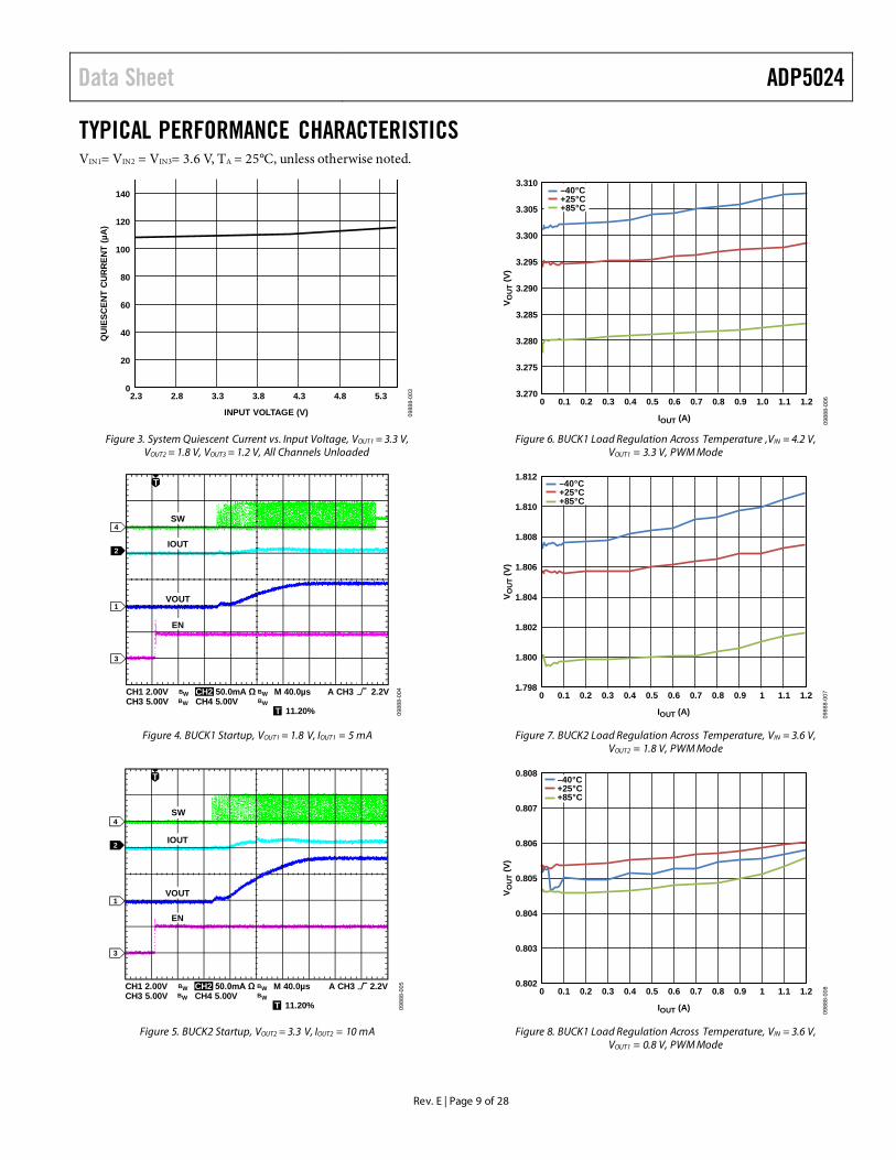
TYPICAL PERFORMANCE CHARACTERISTICS VIN1= VIN2 = VIN3= 3.6 V, TA = 25°C, unless otherwise noted.
0
20
40
60
80
100
120
140
2.3 2.8 3.3 3.8 4.3 4.8 5.3
INPUT VOLTAGE (V)
QU
IESC
ENT
CU
RR
ENT
(µA
)
0988
8-00
3
Figure 3. System Quiescent Current vs. Input Voltage, VOUT1 = 3.3 V, VOUT2 = 1.8 V, VOUT3 = 1.2 V, All Channels Unloaded
4
1
3
T
2
CH1 2.00VCH4 5.00V
M 40.0µs A CH3 2.2V
T 11.20%
BW CH2 50.0mA Ω BWBWCH3 5.00V BW
SW
IOUT
VOUT
EN
0988
8-00
4
Figure 4. BUCK1 Startup, VOUT1 = 1.8 V, IOUT1 = 5 mA
4
1
3
T
2
CH1 2.00VCH4 5.00V
M 40.0µs A CH3 2.2V
T 11.20%
BW CH2 50.0mA Ω BW BWCH3 5.00V BW
SW
IOUT
VOUT
EN
0988
8-00
5
Figure 5. BUCK2 Startup, VOUT2 = 3.3 V, IOUT2 = 10 mA
3.270
3.275
3.280
3.285
3.290
3.295
3.300
3.305
3.310
0 0.1 0.2 0.3 0.4 0.5 0.6 0.7 0.8 0.9 1.0 1.1 1.2
V OU
T (V
)
IOUT (A)
–40°C+25°C+85°C
0988
8-00
6
Figure 6. BUCK1 Load Regulation Across Temperature ,VIN = 4.2 V,
VOUT1 = 3.3 V, PWM Mode
1.798
1.800
1.802
1.804
1.806
1.808
1.810
1.812
0 0.1 0.2 0.3 0.4 0.5 0.6 0.7 0.8 0.9 1 1.1 1.2
V OU
T(V
)
IOUT (A)
–40°C+25°C+85°C
0988
8-00
7
Figure 7. BUCK2 Load Regulation Across Temperature, VIN = 3.6 V, VOUT2 = 1.8 V, PWM Mode
0.802
0.803
0.804
0.805
0.806
0.807
0.808
0 0.1 0.2 0.3 0.4 0.5 0.6 0.7 0.8 0.9 1 1.1 1.2
V OU
T (V
)
IOUT (A)
–40°C+25°C+85°C
0988
8-00
8
Figure 8. BUCK1 Load Regulation Across Temperature, VIN = 3.6 V, VOUT1 = 0.8 V, PWM Mode

ADP5024 Data Sheet
Rev. E | Page 10 of 28
0
10
20
30
40
50
60
70
80
90
100
0.001 0.01 0.1 1
EFFI
CIE
NCY
(%)
IOUT (A)
VIN = 3.9V
VIN = 5.5V
VIN = 4.2V
0988
8-00
9
Figure 9. BUCK1 Efficiency vs. Load Current, Across Input Voltage,
VOUT1 = 3.3 V, Automatic Mode
0
10
20
30
40
50
60
70
80
90
100
0.001 0.01 0.1 1
EFFI
CIE
NCY
(%)
IOUT (A)
VIN = 4.2V
VIN = 5.5V
VIN = 3.9V
0988
8-01
0
Figure 10. BUCK1 Efficiency vs. Load Current, Across Input Voltage, VOUT1 = 3.3 V, PWM Mode
0
10
20
30
40
50
60
70
80
90
100
0.001 0.01 0.1 1
EFFI
CIE
NCY
(%)
IOUT (A)
VIN = 2.3VVIN = 5.5VVIN = 4.2V
VIN = 3.6V
0988
8-01
1
Figure 11. BUCK2 Efficiency vs. Load Current, Across Input Voltage,
VOUT2 = 1.8 V, Automatic Mode
0
10
20
30
40
50
60
70
80
90
100
0.001 0.01 0.1 1
EFFI
CIE
NCY
(%)
IOUT (A)
VIN = 2.3V
VIN = 3.6V
VIN = 4.2V
VIN = 5.5V
0988
8-01
2
Figure 12. BUCK2 Efficiency vs. Load Current, Across Input Voltage,
VOUT2 = 1.8 V, PWM Mode
0
10
20
30
40
50
60
70
80
90
100
0.001 0.01 0.1 1
EFFI
CIE
NC
Y(%
)
IOUT (A)
VIN = 2.3VVIN = 5.5VVIN = 4.2V
VIN = 3.6V
0988
8-01
3
Figure 13. BUCK1 Efficiency vs. Load Current, Across Input Voltage,
VOUT1 = 0.8 V, Automatic Mode
0
10
20
30
40
50
60
70
80
90
100
0.001 0.01 0.1 1
EFFI
CIE
NCY
(%)
IOUT (A)
VIN = 2.3V
VIN = 4.2V
VIN = 5.5V
VIN = 3.6V
0988
8-01
4
Figure 14. BUCK1 Efficiency vs. Load Current, Across Input Voltage,
VOUT1 = 0.8 V, PWM Mode

Data Sheet ADP5024
Rev. E | Page 11 of 28
0
10
20
30
40
50
60
70
80
90
100
0.001 0.01 0.1 1
EFFI
CIE
NCY
(%)
IOUT (A)
–40°C
+25°C
+85°C
0988
8-01
5
Figure 15. BUCK1 Efficiency vs. Load Current, Across Temperature,
VIN = 3.9 V, VOUT1 = 3.3 V, Automatic Mode
0
10
20
30
40
50
60
70
80
90
100
0.001 0.01 0.1 1
EFFI
CIE
NCY
(%)
IOUT (A)
+85°C+25°C
–40°C
0988
8-01
6
Figure 16. BUCK2 Efficiency vs. Load Current, Across Temperature,
VOUT2 = 1.8 V, Automatic Mode
0
10
20
30
40
50
60
70
80
90
100
0.001 0.01 0.1 1
EFFI
CIE
NCY
(%)
IOUT (A)
+85°C
+25°C
–40°C
0988
8-01
7
Figure 17. BUCK1 Efficiency vs. Load Current, Across Temperature,
VOUT1 = 0.8 V, Automatic Mode
2.5
2.6
2.7
2.8
2.9
3.0
3.1
3.2
3.3
0 0.2 0.4 0.6 0.8 1.0 1.2
SCO
PE F
REQ
UEN
CY
(MH
z)
IOUT (A)
+85°C
+25°C
–40°C
0988
8-01
8
Figure 18. BUCK2 Switching Frequency vs. Output Current, Across
Temperature, VOUT2 = 1.8 V, PWM Mode
2
4
T
1
CH1 50mV M 4.00µs A CH2 240mA
T 28.40%
CH2 500mA ΩCH4 2.00V
ISW
VOUT
SW
0988
8-01
9
Figure 19. Typical Waveforms, VOUT1 = 3.3 V, IOUT1 = 30 mA, Automatic Mode
2
4
T
1
CH1 50mV M 4.00µs A CH2 220mA
T 28.40%
BW CH2 500mA ΩCH4 2.00V BW
ISW
VOUT
SW
0988
8-02
0
Figure 20. Typical Waveforms, VOUT2 = 1.8 V, IOUT2 = 30 mA, Automatic Mode
ADP5024 Data Sheet
Rev. E | Page 12 of 28
2
4
T
1
CH1 50mV M 400ns A CH2 220mA
T 28.40%
BW CH2 500mA ΩCH4 2.00V BW
ISW
VOUT
SW
0988
8-02
1
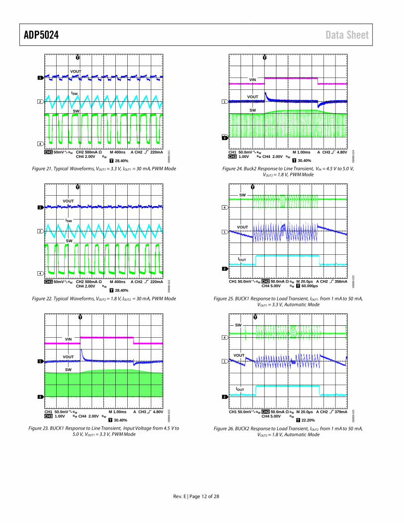
Figure 21. Typical Waveforms, VOUT1 = 3.3 V, IOUT1 = 30 mA, PWM Mode
2
4
T
1
CH1 50mV M 400ns A CH2 220mA
T 28.40%
BW CH2 500mA ΩCH4 2.00V BW
ISW
VOUT
SW
0988
8-02
2
Figure 22. Typical Waveforms, VOUT2 = 1.8 V, IOUT2 = 30 mA, PWM Mode
CH1 50.0mVCH3 1.00V CH4 2.00V
M 1.00ms A CH3 4.80V
1
3
T 30.40%
T
BWBW BW
VOUT
VIN
SW
0988
8-02
3
Figure 23. BUCK1 Response to Line Transient, Input Voltage from 4.5 V to
5.0 V, VOUT1 = 3.3 V, PWM Mode
1
4
T
3
CH1 50.0mVCH3 1.00V CH4 2.00V
M 1.00ms A CH3 4.80V
T 30.40%
BWBW BW
VOUT
VIN
SW
0988
8-02
4
Figure 24. Buck2 Response to Line Transient, VIN = 4.5 V to 5.0 V,
VOUT2 = 1.8 V, PWM Mode
4
1
T
2
CH1 50.0mVCH4 5.00V
M 20.0µs A CH2 356mAT 60.000µs
BW CH2 50.0mA Ω BWBW
VOUT
IOUT
SW
0988
8-02
5
Figure 25. BUCK1 Response to Load Transient, IOUT1 from 1 mA to 50 mA, VOUT1 = 3.3 V, Automatic Mode
4
1
T
2
CH1 50.0mVCH4 5.00V
M 20.0µs A CH2 379mA
T 22.20%
BW CH2 50.0mA Ω BWBW
VOUT
IOUT
SW
0988
8-02
6
Figure 26. BUCK2 Response to Load Transient, IOUT2 from 1 mA to 50 mA,
VOUT2 = 1.8 V, Automatic Mode

Data Sheet ADP5024
Rev. E | Page 13 of 28
4
2
T
1
CH1 50.0mVCH4 5.00V
M 20.0µs A CH2 408mA
T 20.40%
BW CH2 200mA Ω BW BW
VOUT
IOUT
SW
0988
8-02
7
Figure 27. BUCK1 Response to Load Transient, IOUT1 from 20 mA to 180 mA,
VOUT1 = 3.3 V, Automatic Mode
4
2
T
1
CH1 100mVCH4 5.00V
M 20.0µs A CH2 88.0mA
T 19.20%
BW CH2 200mA Ω BW BW
VOUT
IOUT
SW
0988
8-02
8
Figure 28. BUCK2 Response to Load Transient, IOUT2 from 20 mA to 180 mA, VOUT2 = 1.8 V, Automatic Mode
4
1
3
T
2
CH1 5.00VCH4 5.00V
M 400ns A CH4 1.90V
T 50.00%
BW CH2 5.00V BW BWCH3 5.00V BW
VOUT1
VOUT2
SW1
SW2
0988
8-02
9
Figure 29. VOUTx and SW Waveforms for BUCK1 and BUCK2 in PWM Mode Showing Out-of-Phase Operation
CH1 100mA CH2 5V M40µs 2.5GS/s1M Points
A CH2 4.20VT 159.4µsCH3 1V
2
3
1
EN
VOUT
IIN
0988
8-03
0
Figure 30. LDO Startup, VOUT3 = 1.8 V
3.294
3.295
3.296
3.297
3.298
3.299
3.300
3.301
3.302
3.303
3.304
0 0.1 0.2 0.3
V OU
T (V
)
IOUT (A)
VIN = 3.8VVIN = 4.2VVIN = 5.5V
0988
8-03
1
Figure 31. LDO Load Regulation Across Input Voltage, VOUT3 = 3.3 V
0
50
100
150
200
250
300
350
400
2.3 2.8 3.3 3.8 4.3 4.8 5.3
RD
S ON
(mΩ
)
INPUT VOLTAGE (V)
+25°C+125°C
–40°C
0988
8-03
2
Figure 32. NMOS RDSON vs. Input Voltage Across Temperature

ADP5024 Data Sheet
Rev. E | Page 14 of 28
2.3 2.8 3.3 3.8 4.3 4.8 5.3
RD
S ON
(mΩ
)
INPUT VOLTAGE (V)
+125°C+25°C
–40°C
0
50
100
150
200
250
0988
8-03
3
Figure 33. PMOS RDSON vs. Input Voltage Across Temperature
1.792
1.793
1.794
1.795
1.796
1.797
1.798
1.799
1.800
1.801
1.802
0 0.1 0.2 0.3
V OU
T (V
)
IOUT (A)
–40°C+25°C+85°C
0988
8-03
4
Figure 34. LDO Load Regulation Across Temperature, VIN3 = 3.6 V, VOUT3 = 1.8 V
0
0.5
1.0
1.5
2.0
2.5
3.0
2.4 2.6 2.8 3.0 3.2 3.4 3.6 3.8 4.0 4.2 4.4 4.6 4.8 5.0 5.2 5.4
VIN (V)
IOUT = 300mAIOUT = 150mA
IOUT = 100mAIOUT = 1mA
IOUT = 10mA IOUT = 100µA
0988
8-03
5
V OU
T(V
)
Figure 35. LDO Line Regulation Across Output Load, VOUT3 = 2.8 V
0 0.05 0.10 0.15 0.20 0.25
GR
OU
ND
CU
RR
ENT
(µA
)
LOAD CURRENT (A)
0
5
10
15
20
25
30
35
40
45
50
0988
8-03
6
Figure 36. LDO Ground Current vs. Output Load, VIN3 = 3.3 V, VOUT3 = 2.8 V
2
T
1
CH1 100mV M 40.0µs A CH2 52.0mA
T 19.20%
BW CH2 100mA Ω BW
VOUT
IOUT
0988
8-03
7
Figure 37. LDO Response to Load Transient, IOUT3 from 1 mA to 80 mA, VOUT3 = 2.8 V
2
3
T
1
CH1 20.0mVCH3 1.00V
M 100µs A CH3 4.80V
T 28.40%
VOUT
VIN
0988
8-03
8
Figure 38. LDO Response to Line Transient, Input Voltage from 4.5 V to 5 V, VOUT3 = 2.8 V

Data Sheet ADP5024
Rev. E | Page 15 of 28
60
55
50
45
40
35
30
250.001 0.01 0.1 1 10 100
ILOAD (mA)
RM
S N
OIS
E (µ
V)
VIN = 3.3V
VIN = 5V
0988
8-03
9
Figure 39. LDO Output Noise vs. Load Current, Across Input Voltage,
VOUT3 = 2.8 V
60
65
55
50
45
40
35
30
250.001 0.01 0.1 1 10 100
ILOAD (mA)
RM
S N
OIS
E (µ
V)
VIN = 3.3V
VIN = 5V
0988
8-04
0
Figure 40. LDO Output Noise vs. Load Current, Across Input Voltage,
VOUT3 = 3.0 V
0
–10
–20
–30
–40
–50
–60
–70
–80
–90
–10010 100 1k 10k 100k 1M 10M
FREQUENCY (Hz)
PSR
R (d
B)
100µA1mA10mA50mA100mA150mA
0988
8-04
1
Figure 41. LDO PSRR Across Output Load, VIN3 = 3.3 V, VOUT3 = 2.8 V
0
–20
–40
–60
–80
–100
–12010 100 1k 10k 100k 1M 10M
FREQUENCY (Hz)
PSR
R (d
B)
100µA1mA10mA50mA100mA150mA
0988
8-04
2
Figure 42. LDO PSRR Across Output Load, VIN3 = 3.3 V, VOUT3 = 3.0 V
0
–20
–40
–60
–80
–100
–12010 100 1k 10k 100k 1M 10M
FREQUENCY (Hz)
PSR
R (d
B)
100µA1mA10mA50mA100mA150mA
0988
8-04
3
Figure 43. LDO PSRR Across Output Load, VIN3 = 5.0 V, VOUT3 = 2.8 V
0
–10
–20
–30
–40
–50
–60
–70
–80
–90
–10010 100 1k 10k 100k 1M 10M
FREQUENCY (Hz)
PSR
R (d
B)
100µA1mA10mA50mA100mA150mA
0988
8-04
4
Figure 44. LDO PSRR Across Output Load, VIN3 = 5.0 V, VOUT3 = 3.0 V
ADP5024 Data Sheet
Rev. E | Page 16 of 28
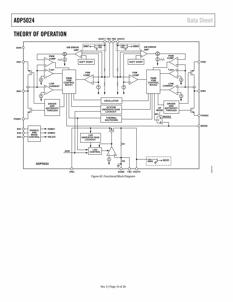
THEORY OF OPERATION
LDOCONTROL
LDOUNDERVOLTAGE
LOCKOUT
SOFT START
PWM/PSM
CONTROLBUCK2
DRIVERAND
ANTISHOOTTHROUGH
SOFT START
DRIVERAND
ANTISHOOTTHROUGH
OSCILLATOR
THERMALSHUTDOWN
SYSTEMUNDERVOLTAGE
LOCKOUT
PWMCOMP
GM ERRORAMP
GM ERRORAMP
PSMCOMP
PSMCOMP
LOWCURRENT
ILIMIT
PWMCOMP
LOWCURRENT
ILIMIT
R1
R2ADP5024
VOUT1 VOUT2
VIN1
AVIN
SW1
PGND1
VIN3 AGND VOUT3FB3
PGND2
SW2
VIN2
AVIN
75ΩENBK1
ENABLEAND
MODECONTROL
EN1 ENBK1
ENBK2
ENLDO
75Ω ENBK2
EN2
EN3
600Ω ENLDO
B
SEL
OPMODE
MODE2
AY
MODE
FB1 FB2
PWM/PSM
CONTROLBUCK1
0988
8-04
5
Figure 45. Functional Block Diagram

Data Sheet ADP5024
Rev. E | Page 17 of 28
POWER MANAGEMENT UNIT The ADP5024 is a micropower management unit (microPMU) combing two step-down (buck) dc-to-dc convertors and one low dropout linear regulator (LDO). The high switching frequency and tiny 24-lead LFCSP package allow for a small power manage-ment solution.
To combine these high performance regulators into the microPMU, there is a system controller allowing them to operate together.
The buck regulators can operate in forced PWM mode if the MODE pin is at a logic level high. In forced PWM mode, the buck switching frequency is always constant and does not change with the load current. If the MODE pin is at logic level low, the switching regulators operate in automatic PWM/PSM mode. In this mode, the regulators operate at a fixed PWM frequency when the load current is above the PSM current threshold. When the load current falls below the PSM current threshold, the regulator in question enters PSM, where the switching occurs in bursts. The burst repetition rate is a function of the current load and the output capacitor value. This operating mode reduces the switching and quiescent current losses. The automatic PWM/PSM mode transition is controlled independently for each buck regulator. The two bucks operate synchronized to each other.
The ADP5024 has individual enable pins (EN1 to EN3) that control the activation of each regulator. The regulators are activated by a logic level high applied to the respective EN pin, wherein EN1 controls BUCK1, EN2 controls BUCK2, and EN3 controls the LDO.
Regulator output voltages are set through external resistor dividers or can be optionally factory programmed to default values (see the Ordering Guide section).
When a regulator is turned on, the output voltage ramp rate is controlled though a soft start circuit to avoid a large inrush current due to the charging of the output capacitors.
Thermal Protection
In the event that the junction temperature rises above 150°C, the thermal shutdown circuit turns off all of the regulators. Extreme junction temperatures can be the result of high current operation, poor circuit board design, or high ambient tempera-ture. A 20°C hysteresis is included so that when thermal shutdown
occurs, the regulators do not return to operation until the on-chip temperature drops below 130°C. When emerging from thermal shutdown, all regulators restart with soft start control.
Undervoltage Lockout
To protect against battery discharge, undervoltage lockout (UVLO) circuitry is integrated in the system. If the input voltage on AVIN drops below a typical 2.15 V UVLO threshold, all channels shut down. In the buck channels, both the power switch and the synchronous rectifier turn off. When the voltage on AVIN rises above the UVLO threshold, the part is enabled once more.
Alternatively, the user can select device models with a UVLO set at a higher level, suitable for 5 V supply applications. For these models, the device reaches the turn off threshold when the input supply drops to 3.65 V typical.
In case of a thermal or UVLO event, the active pull-downs (if factory enabled) are enabled to discharge the output capacitors quickly. The pull-down resistors remain engaged until the thermal fault event is no longer present or the input supply voltage falls below the VPOR voltage level. The typical value of VPOR is approx-imately 1 V.
Enable/Shutdown
The ADP5024 has an individual control pin for each regulator. A logic level high applied to the ENx pin activates a regulator whereas a logic level low turns off a regulator.
Figure 46 shows the regulator activation timings for the ADP5024 when all enable pins are connected to AVIN. Also shown is the active pull-down activation.

ADP5024 Data Sheet
Rev. E | Page 18 of 28
AVIN
VOUT3
VOUT1
VUVLO
VOUT2
VPOR
BUCK2PULL-DOWN
BUCK1, LDOPULL-DOWNS
50µs (MIN)
30µs(MIN) 50µs (MIN)
30µs(MIN)
0988
8-04
6
Figure 46. Regulator Sequencing (EN1 = EN2 = EN3 = VAVIN)
Data Sheet ADP5024
Rev. E | Page 19 of 28
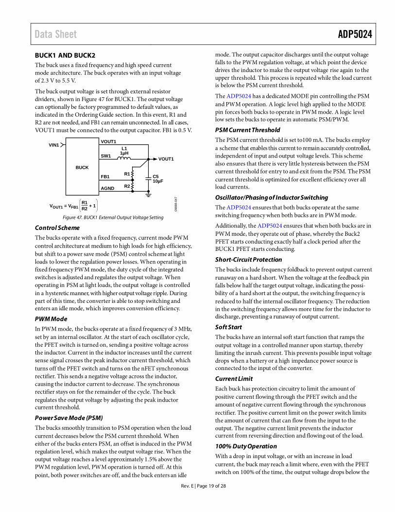
BUCK1 AND BUCK2 The buck uses a fixed frequency and high speed current mode architecture. The buck operates with an input voltage of 2.3 V to 5.5 V.
The buck output voltage is set through external resistor dividers, shown in Figure 47 for BUCK1. The output voltage can optionally be factory programmed to default values, as indicated in the Ordering Guide section. In this event, R1 and R2 are not needed, and FB1 can remain unconnected. In all cases, VOUT1 must be connected to the output capacitor. FB1 is 0.5 V.
BUCK
AGND
FB1
SW1
R1
R2
VOUT1
VOUT1
VIN1L1
1µH
C510µF
VOUT1 = VFB1 + 1R1R2 09
888-
047
Figure 47. BUCK1 External Output Voltage Setting
Control Scheme
The bucks operate with a fixed frequency, current mode PWM control architecture at medium to high loads for high efficiency, but shift to a power save mode (PSM) control scheme at light loads to lower the regulation power losses. When operating in fixed frequency PWM mode, the duty cycle of the integrated switches is adjusted and regulates the output voltage. When operating in PSM at light loads, the output voltage is controlled in a hysteretic manner, with higher output voltage ripple. During part of this time, the converter is able to stop switching and enters an idle mode, which improves conversion efficiency.
PWM Mode
In PWM mode, the bucks operate at a fixed frequency of 3 MHz, set by an internal oscillator. At the start of each oscillator cycle, the PFET switch is turned on, sending a positive voltage across the inductor. Current in the inductor increases until the current sense signal crosses the peak inductor current threshold, which turns off the PFET switch and turns on the nFET synchronous rectifier. This sends a negative voltage across the inductor, causing the inductor current to decrease. The synchronous rectifier stays on for the remainder of the cycle. The buck regulates the output voltage by adjusting the peak inductor current threshold.
Power Save Mode (PSM)
The bucks smoothly transition to PSM operation when the load current decreases below the PSM current threshold. When either of the bucks enters PSM, an offset is induced in the PWM regulation level, which makes the output voltage rise. When the output voltage reaches a level approximately 1.5% above the PWM regulation level, PWM operation is turned off. At this point, both power switches are off, and the buck enters an idle
mode. The output capacitor discharges until the output voltage falls to the PWM regulation voltage, at which point the device drives the inductor to make the output voltage rise again to the upper threshold. This process is repeated while the load current is below the PSM current threshold.
The ADP5024 has a dedicated MODE pin controlling the PSM and PWM operation. A logic level high applied to the MODE pin forces both bucks to operate in PWM mode. A logic level low sets the bucks to operate in automatic PSM/PWM.
PSM Current Threshold
The PSM current threshold is set to100 mA. The bucks employ a scheme that enables this current to remain accurately controlled, independent of input and output voltage levels. This scheme also ensures that there is very little hysteresis between the PSM current threshold for entry to and exit from the PSM. The PSM current threshold is optimized for excellent efficiency over all load currents.
Oscillator/Phasing of Inductor Switching
The ADP5024 ensures that both bucks operate at the same switching frequency when both bucks are in PWM mode.
Additionally, the ADP5024 ensures that when both bucks are in PWM mode, they operate out of phase, whereby the Buck2 PFET starts conducting exactly half a clock period after the BUCK1 PFET starts conducting.
Short-Circuit Protection
The bucks include frequency foldback to prevent output current runaway on a hard short. When the voltage at the feedback pin falls below half the target output voltage, indicating the possi-bility of a hard short at the output, the switching frequency is reduced to half the internal oscillator frequency. The reduction in the switching frequency allows more time for the inductor to discharge, preventing a runaway of output current.
Soft Start
The bucks have an internal soft start function that ramps the output voltage in a controlled manner upon startup, thereby limiting the inrush current. This prevents possible input voltage drops when a battery or a high impedance power source is connected to the input of the converter.
Current Limit
Each buck has protection circuitry to limit the amount of positive current flowing through the PFET switch and the amount of negative current flowing through the synchronous rectifier. The positive current limit on the power switch limits the amount of current that can flow from the input to the output. The negative current limit prevents the inductor current from reversing direction and flowing out of the load.
100% Duty Operation
With a drop in input voltage, or with an increase in load current, the buck may reach a limit where, even with the PFET switch on 100% of the time, the output voltage drops below the
ADP5024 Data Sheet
Rev. E | Page 20 of 28
desired output voltage. At this limit, the buck transitions to a mode where the PFET switch stays on 100% of the time. When the input conditions change again and the required duty cycle falls, the buck immediately restarts PWM regulation without allowing overshoot on the output voltage.
Active Pull-Down Resistors
All regulators have optional, factory programmable, active pull-down resistors discharging the respective output capacitors when the regulators are disabled. The pull-down resistors are connected between VOUTx and AGND. Active pull-downs are disabled when the regulators are turned on. The typical value of the pull-down resistor is 600 Ω for the LDO and 75 Ω for each buck. Figure 46 shows the activation timings for the active pull-downs during regulator activation and deactivation.
LDO The ADP5024 contains one LDO with low quiescent current and low dropout voltage and provides up to 300 mA of output current. Drawing a low 10 μA quiescent current (typical) at no load makes the LDO ideal for battery-operated portable equipment.
The LDO operates with an input voltage of 1.7 V to 5.5 V. The wide operating range makes the LDO suitable for cascading
configurations where the LDO supply voltage is provided from one of the buck regulators.
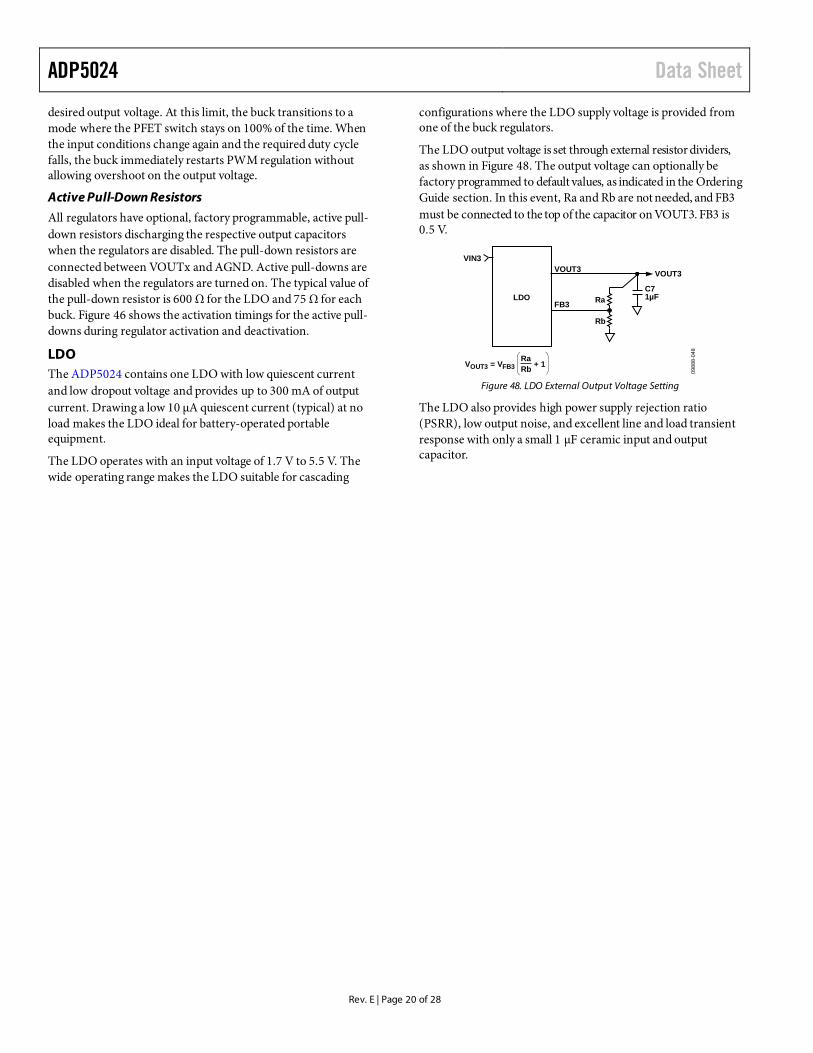
The LDO output voltage is set through external resistor dividers, as shown in Figure 48. The output voltage can optionally be factory programmed to default values, as indicated in the Ordering Guide section. In this event, Ra and Rb are not needed, and FB3 must be connected to the top of the capacitor on VOUT3. FB3 is 0.5 V.
LDOFB3 Ra
Rb
VOUT3 VOUT3
VIN3
C71µF
VOUT3 = VFB3 + 1RaRb 09
888-
048
Figure 48. LDO External Output Voltage Setting
The LDO also provides high power supply rejection ratio (PSRR), low output noise, and excellent line and load transient response with only a small 1 µF ceramic input and output capacitor.

Data Sheet ADP5024
Rev. E | Page 21 of 28
APPLICATIONS INFORMATION BUCK EXTERNAL COMPONENT SELECTION Trade-offs between performance parameters such as efficiency and transient response can be made by varying the choice of external components in the applications circuit, as shown in Figure 1.
Feedback Resistors
For the adjustable model, shown in Figure 47, the total combined resistance for R1 and R2 is not to exceed 400 kΩ.
Inductor
The high switching frequency of the ADP5024 bucks allows for the selection of small chip inductors. For best performance, use inductor values between 0.7 μH and 3 μH. Suggested inductors are shown in Table 9.
The peak-to-peak inductor current ripple is calculated using the following equation:
LfVVVV
ISWIN
OUTINOUTRIPPLE ××
−×=
)(
where: fSW is the switching frequency. L is the inductor value.
The minimum dc current rating of the inductor must be greater than the inductor peak current. The inductor peak current is calculated using the following equation:
2)(RIPPLE
MAXLOADPEAKI
II +=
Inductor conduction losses are caused by the flow of current through the inductor, which has an associated internal dc resistance (DCR). Larger sized inductors have smaller DCR, which may decrease inductor conduction losses. Inductor core losses are related to the magnetic permeability of the core material. Because the bucks are high switching frequency dc-to-dc converters, shielded ferrite core material is recommended for its low core losses and low EMI.
Output Capacitor
Higher output capacitor values reduce the output voltage ripple and improve load transient response. When choosing this value, it is also important to account for the loss of capacitance due to output voltage dc bias.
Ceramic capacitors are manufactured with a variety of dielec-trics, each with a different behavior over temperature and applied voltage. Capacitors must have a dielectric that is adequate to ensure the minimum capacitance over the necessary temperature range and dc bias conditions. X5R or X7R dielectrics with a voltage rating of 6.3 V or 10 V are recommended for best per-formance. Y5V and Z5U dielectrics are not recommended for use with any dc-to-dc converter because of their poor temperature and dc bias characteristics.
The worst-case capacitance accounting for capacitor variation over temperature, component tolerance, and voltage is calcu-lated using the following equation:
CEFF = COUT × (1 − TEMPCO) × (1 − TOL)
where: CEFF is the effective capacitance at the operating voltage. TEMPCO is the worst-case capacitor temperature coefficient. TOL is the worst-case component tolerance.
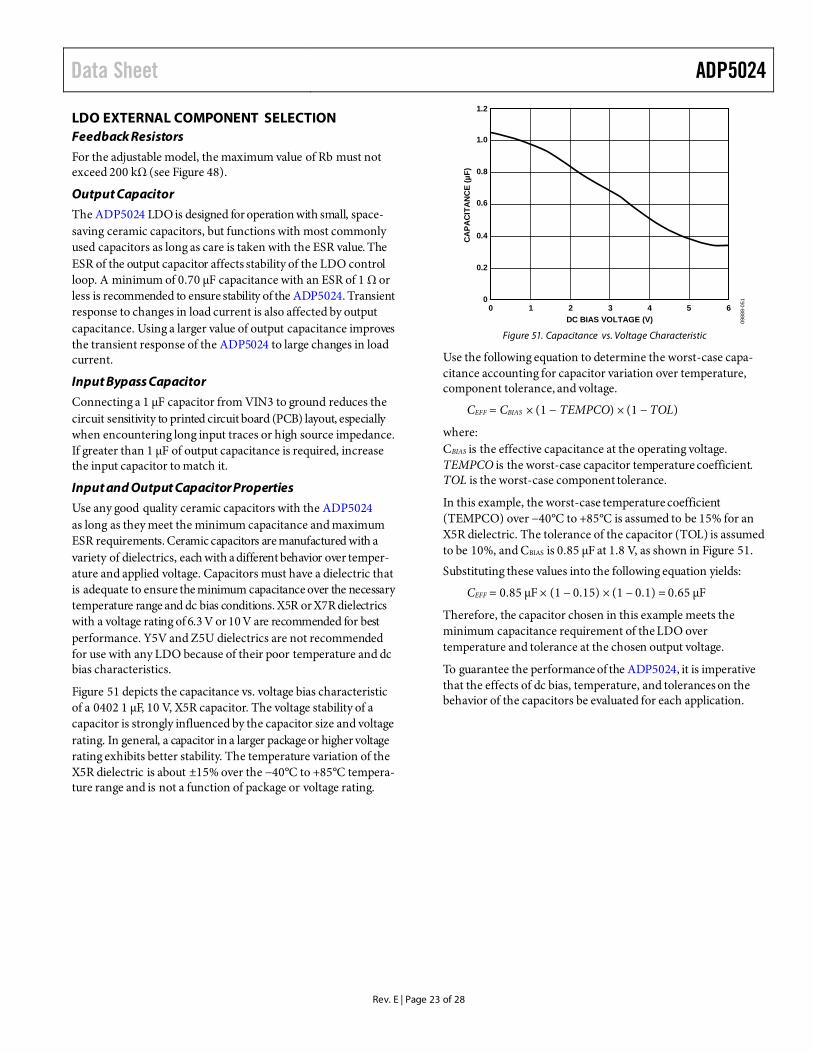
In this example, the worst-case temperature coefficient (TEMPCO) over −40°C to +85°C is assumed to be 15% for an X5R dielectric. The tolerance of the capacitor (TOL) is assumed to be 10%, and COUT is 9.2 μF at 1.8 V, as shown in Figure 49.
Substituting these values in the equation yields
CEFF = 9.2 μF × (1 − 0.15) × (1 − 0.1) ≈ 7.0 μF
To guarantee the performance of the bucks, it is imperative that the effects of dc bias, temperature, and tolerances on the behavior of the capacitors be evaluated for each application.
0
2
4
6
8
10
12
0 1 2 3 4 5 6
DC BIAS VOLTAGE (V)
CA
PAC
ITA
NC
E (µ
F)
0988
8-04
9
Figure 49. Capacitance vs. Voltage Characteristic
Table 9. Suggested 1.0 μH Inductors Vendor Model Dimensions (mm) ISAT (mA) DCR (mΩ) Murata LQM2MPN1R0NG0B 2.0 × 1.6 × 0.9 1400 85
Murata LQH32PN1R0NN0 3.2 × 2.5 × 1.6 2300 45 Taiyo Yuden CBC3225T1R0MR 3.2 × 2.5 × 2.5 2000 71 Coilcraft XFL4020-102ME 4.0 × 4.0 × 2.1 5400 11
Coilcraft XPL2010-102ML 1.9 × 2.0 × 1.0 1800 89 Toko MDT2520-CN 2.5 × 2.0 × 1.2 1350 85

ADP5024 Data Sheet
Rev. E | Page 22 of 28
The peak-to-peak output voltage ripple for the selected output capacitor and inductor values is calculated using the following equation:
( ) OUTSW
IN
OUTSW
RIPPLERIPPLE CLf
VCf
IV
×××π≈
××= 228
Capacitors with lower equivalent series resistance (ESR) are preferred to guarantee low output voltage ripple, as shown in the following equation:
RIPPLE
RIPPLECOUT I
VESR ≤
The effective capacitance needed for stability, which includes temperature and dc bias effects, is a minimum of 7 µF and a maximum of 40 µF.
The buck regulators require 10 µF output capacitors to guarantee stability and response to rapid load variations and to transition into and out of the PWM/PSM modes. A list of suggested capaci-tors is shown in Table 10. In certain applications where one or both buck regulator powers a processor, the operating state is known because it is controlled by software. In this condition, the processor can drive the MODE pin according to the operating state; consequently, it is possible to reduce the output capacitor from 10 µF to 4.7 µF because the regulator does not expect a large load variation when working in PSM mode (see Figure 50).
Input Capacitor Higher value input capacitors help to reduce the input voltage ripple and improve transient response. Maximum input capacitor current is calculated using the following equation:
IN
OUTINOUTMAXLOADCIN V
VVVII
)()(
−≥
To minimize supply noise, place the input capacitor as close as possible to the VINx pin of the buck. As with the output capa-citor, a low ESR capacitor is recommended.
A 4.7 µF capacitor is recommended for a typical application; depending on the application, a smaller or larger output capacitor may be chosen. A list of suggested 4.7 µF capacitors is shown in Table 11. The effective capacitance needed for stability, which includes temperature and dc bias effects, is a minimum of 3 µF and a maximum of 10 µF.
Table 10. Suggested 10 μF Capacitors
Vendor Type Model Case Size
Voltage Rating (V)
Murata X5R GRM188R60J106 0603 6.3 TDK X5R C1608JB0J106K 0603 6.3 Panasonic X5R ECJ1VB0J106M 0603 6.3
Table 11. Suggested 4.7 μF Capacitors
Vendor Type Model Case Size
Voltage Rating (V)
Murata X5R GRM188R60J475ME19D 0402 6.3 Taiyo Yuden X5R JMK107BJ475 0402 6.3 Panasonic X5R ECJ-0EB0J475M 0402 6.3
Table 12. Suggested 1.0 μF Capacitors
Vendor Type Model Case Size
Voltage Rating (V)
Murata X5R GRM155B30J105K 0402 6.3 TDK X5R C1005JB0J105KT 0402 6.3
Panasonic X5R ECJ0EB0J105K 0402 6.3 Taiyo Yuden
X5R LMK105BJ105MV-F 0402 10.0
VIN1
VIN3
EN1PWM
PSM/PWM
2.3V TO5.5V
SW1
FB1
R2
R1
VOUT1
PGND1
MODE
C510µF
VOUT1 AT1200mA
L1 1µH
EN1
BUCK1
MODE
C31µF
C24.7µF
C14.7µF
AVINCAVIN0.1µF
VIN2
EN2
AGND
EN2
BUCK2
MODE
EN3
1.7V TO5.5V
ONOFF
ONOFF
EN3 LDO(ANALOG)
ADP5024
HOUSEKEEPING
SW2FB2
R4
R3
VOUT2
PGND2C610µF
VOUT2 AT1200mA
L2 1µH
FB3
R6
R5VOUT3
C71µF
VOUT3 AT300mA
0988
8-05
0
Figure 50. Processor System Power Management with PSM/PWM Control
Data Sheet ADP5024
Rev. E | Page 23 of 28
LDO EXTERNAL COMPONENT SELECTION Feedback Resistors
For the adjustable model, the maximum value of Rb must not exceed 200 kΩ (see Figure 48).
Output Capacitor
The ADP5024 LDO is designed for operation with small, space-saving ceramic capacitors, but functions with most commonly used capacitors as long as care is taken with the ESR value. The ESR of the output capacitor affects stability of the LDO control loop. A minimum of 0.70 µF capacitance with an ESR of 1 Ω or less is recommended to ensure stability of the ADP5024. Transient response to changes in load current is also affected by output capacitance. Using a larger value of output capacitance improves the transient response of the ADP5024 to large changes in load current.
Input Bypass Capacitor
Connecting a 1 µF capacitor from VIN3 to ground reduces the circuit sensitivity to printed circuit board (PCB) layout, especially when encountering long input traces or high source impedance. If greater than 1 µF of output capacitance is required, increase the input capacitor to match it.
Input and Output Capacitor Properties
Use any good quality ceramic capacitors with the ADP5024 as long as they meet the minimum capacitance and maximum ESR requirements. Ceramic capacitors are manufactured with a variety of dielectrics, each with a different behavior over temper-ature and applied voltage. Capacitors must have a dielectric that is adequate to ensure the minimum capacitance over the necessary temperature range and dc bias conditions. X5R or X7R dielectrics with a voltage rating of 6.3 V or 10 V are recommended for best performance. Y5V and Z5U dielectrics are not recommended for use with any LDO because of their poor temperature and dc bias characteristics.
Figure 51 depicts the capacitance vs. voltage bias characteristic of a 0402 1 µF, 10 V, X5R capacitor. The voltage stability of a capacitor is strongly influenced by the capacitor size and voltage rating. In general, a capacitor in a larger package or higher voltage rating exhibits better stability. The temperature variation of the X5R dielectric is about ±15% over the −40°C to +85°C tempera-ture range and is not a function of package or voltage rating.
1.2
1.0
0.8
0.6
0.4
0.2
00 1 2 3 4 5 6
DC BIAS VOLTAGE (V)
CA
PAC
ITA
NC
E (µ
F)
0988
8-05
1
Figure 51. Capacitance vs. Voltage Characteristic
Use the following equation to determine the worst-case capa-citance accounting for capacitor variation over temperature, component tolerance, and voltage.
CEFF = CBIAS × (1 − TEMPCO) × (1 − TOL)
where: CBIAS is the effective capacitance at the operating voltage. TEMPCO is the worst-case capacitor temperature coefficient. TOL is the worst-case component tolerance.
In this example, the worst-case temperature coefficient (TEMPCO) over −40°C to +85°C is assumed to be 15% for an X5R dielectric. The tolerance of the capacitor (TOL) is assumed to be 10%, and CBIAS is 0.85 μF at 1.8 V, as shown in Figure 51.
Substituting these values into the following equation yields:
CEFF = 0.85 μF × (1 − 0.15) × (1 − 0.1) = 0.65 μF
Therefore, the capacitor chosen in this example meets the minimum capacitance requirement of the LDO over temperature and tolerance at the chosen output voltage.
To guarantee the performance of the ADP5024, it is imperative that the effects of dc bias, temperature, and tolerances on the behavior of the capacitors be evaluated for each application.

ADP5024 Data Sheet
Rev. E | Page 24 of 28
POWER DISSIPATION AND THERMAL CONSIDERATIONS The ADP5024 is a highly efficient micropower management unit (microPMU), and, in most cases, the power dissipated in the device is not a concern. However, if the device operates at high ambient temperatures and maximum loading condition, the junction temperature can reach the maximum allowable operating limit (125°C).
When the temperature exceeds 150°C, the ADP5024 turns off all of the regulators allowing the device to cool down. When the die temperature falls below 130°C, the ADP5024 resumes normal operation.
This section provides guidelines to calculate the power dissi-pated in the device and ensure that the ADP5024 operates below the maximum allowable junction temperature.
The efficiency for each regulator on the ADP5024 is given by
100%×=IN
OUT
PP
η (1)
where: η is the efficiency. PIN is the input power. POUT is the output power.
Power loss is given by
PLOSS = PIN − POUT (2a)
or
PLOSS = POUT (1− η)/η (2b)
Power dissipation can be calculated in several ways. The most intuitive and practical is to measure the power dissipated at the input and at all of the outputs. Perform the measurements at the worst-case conditions (voltages, currents, and temperature). The difference between input and output power is dissipated in the device and the inductor. Use Equation 4 to derive the power lost in the inductor, and from this result use Equation 3 to calculate the power dissipation in the ADP5024 buck converter.
A second method to estimate the power dissipation uses the effi-ciency curves provided for the buck regulator, and the power lost on the LDO can be calculated using Equation 12. When the buck efficiency is known, use Equation 2b to derive the total power lost in the buck regulator and inductor, use Equa-tion 4 to derive the power lost in the inductor, and then calculate the power dissipation in the buck converter using Equation 3. Add the power dissipated in the buck and in the LDO to find the total dissipated power.
Note that the buck efficiency curves are typical values and may not be provided for all possible combinations of VIN, VOUT, and IOUT. To account for these variations, it is necessary to include a safety margin when calculating the power dissipated in the buck.
A third way to estimate the power dissipation is analytical and involves modeling the losses in the buck circuit provided by Equation 8 to Equation 11 and calculating the losses in the LDO provided by Equation 12.
BUCK REGULATOR POWER DISSIPATION The power loss of the buck regulator is approximated by
PLOSS = PDBUCK + PL (3)
where: PDBUCK is the power dissipation on one of the ADP5024 buck regulators. PL is the inductor power loss.
The inductor losses are external to the device and they do not have any effect on the die temperature.
The inductor losses are estimated (without core losses) by
PL ≈ IOUT1(RMS)2 × DCRL (4)
where: DCRL is the inductor series resistance. IOUT1(RMS) is the rms load current of the buck regulator.
12+1)(
rII OUT1RMSOUT1 ×= (5)
where r is the normalized inductor ripple current.
r = VOUT1 × (1 − D)/(IOUT1 × L × fSW) (6)
where: L is the inductance. fSW is the switching frequency. D is the duty cycle.
D = VOUT1/VIN1 (7)
The buck regulator power dissipation, PDBUCK, of the ADP5024 includes the power switch conductive losses, the switch losses, and the transition losses of each channel. There are other sources of loss, but these are generally less significant at high output load currents, where the thermal limit of the application is located. Equation 8 captures the calculation that must be made to estimate the power dissipation in the buck regulator.
PDBUCK = PCOND + PSW + PTRAN (8)
The power switch conductive losses are due to the output current, IOUT1, flowing through the P-MOSFET and the N-MOSFET power switches that have internal resistance, RDSON-P and RDSON-N. The amount of conductive power loss is found by
PCOND = [RDSON-P × D + RDSON-N × (1 − D)] × IOUT1(RMS)2 (9)
where RDSON-P is approximately 0.2 Ω, and RDSON-N is approxi-mately 0.16 Ω at a junction temperature of 25°C and VIN1 = VIN2 = 3.6 V. At VIN1 = VIN2 = 2.3 V, these values change to 0.31 Ω and 0.21 Ω, respectively, and at VIN1 = VIN2 = 5.5 V, the values are 0.16 Ω and 0.14 Ω, respectively.

Data Sheet ADP5024
Rev. E | Page 25 of 28
Switching losses are associated with the current drawn by the driver to turn on and turn off the power devices at the switching frequency. The amount of switching power loss is given by
PSW = (CGATE-P + CGATE-N) × VIN12 × fSW (10)
where: CGATE-P is the P-MOSFET gate capacitance. CGATE-N is the N-MOSFET gate capacitance.
For the ADP5024, the total of (CGATE-P + CGATE-N) is approx-imately 150 pF.
The transition losses occur because the P-channel power MOSFET cannot be turned on or off instantaneously, and the SW node takes some time to slew from near ground to near VOUT1 (and from VOUT1 to ground). The amount of transition loss is calculated by
PTRAN = VIN1 × IOUT1 × (tRISE + tFALL) × fSW (11)
where tRISE and tFALL are the rise time and the fall time of the switching node, SW. For the ADP5024, the rise and fall times of SW are in the order of 5 ns.
If the preceding equations and parameters are used for estimating the converter efficiency, it must be noted that the equations do not describe all of the converter losses, and the parameter values given are typical numbers. The converter performance also depends on the choice of passive components and board layout; therefore, include a sufficient safety margin in the estimate.
LDO Regulator Power Dissipation
The power loss of the LDO regulator is given by
PDLDO = [(VIN − VOUT) × ILOAD] + (VIN × IGND) (12)
where: ILOAD is the load current of the LDO regulator. VIN and VOUT are input and output voltages of the LDO, respectively. IGND is the ground current of the LDO regulator.
Power dissipation due to the ground current is small, and it can be ignored.
JUNCTION TEMPERATURE In cases where the board temperature, TA, is known, the thermal resistance parameter, θJA, can be used to estimate the junction temperature rise. TJ is calculated from TA and PD using the formula
TJ = TA + (PD × θJA) (14)
The typical θJA value for the 24-lead, 4 mm × 4 mm LFCSP is 35°C/W (see Table 7). A very important factor to consider is that θJA is based on a 4-layer, 4 in × 3 in, 2.5 oz copper, as per JEDEC standard, and real applications may use different sizes and layers. To remove heat from the device, it is important to maximize the use of copper. Copper exposed to air dissipates heat better than copper used in the inner layers. Connect the exposed pad to the ground plane with several vias.
If the case temperature can be measured, the junction temperature is calculated by
TJ = TC + (PD × θJC) (15)
where TC is the case temperature and θJC is the junction-to-case thermal resistance provided in Table 7.
When designing an application for a particular ambient temperature range, calculate the expected ADP5024 power dissipation (PD) due to the losses of all channels by using Equation 8 to Equation 13. From this power calculation, the junction temperature, TJ, can be estimated using Equation 14.
The reliable operation of the converter and the LDO regulator can be achieved only if the estimated die junction temperature of the ADP5024 (see Equation 14) is less than 125°C. Reliability and mean time between failures (MTBF) is highly affected by increasing the junction temperature. Additional information about product reliability can be found from the ADI Reliability Handbook, which is available at the following URL: www.analog.com/reliability_handbook.
The total power dissipation in the ADP5024 simplifies to
PD = PDBUCK1 + PDBUCK2 + PDLDO (13)

ADP5024 Data Sheet
Rev. E | Page 26 of 28
PCB LAYOUT GUIDELINES Poor layout can affect ADP5024 performance, causing electro-magnetic interference (EMI) and electromagnetic compatibility (EMC) problems, ground bounce, and voltage losses. Poor layout can also affect regulation and stability. A good layout is implemented using the following guidelines. Also, refer to User Guide UG-271.
• Place the inductor, input capacitor, and output capacitor close to the IC using short tracks. These components carry high switching frequencies, and large tracks act as antennas.
• Route the output voltage path away from the inductor and SW node to minimize noise and magnetic interference.
• Maximize the size of ground metal on the component side to help with thermal dissipation.
• Use a ground plane with several vias connected to the component side ground to further reduce noise interference on sensitive circuit nodes.
• Connect VIN1, VIN2, and AVIN together close to the IC using short tracks.

Data Sheet ADP5024
Rev. E | Page 27 of 28
TYPICAL APPLICATION SCHEMATICS
VIN1
VIN3
EN1PWM
PSM/PWM
2.3V TO5.5V
SW1
FB1
VOUT1
PGND1
MODE
C510µF
VOUT1 AT1200mA
L1 1µH
EN1
BUCK1
MODE
C31µF
C24.7µF
C14.7µF
AVINCAVIN0.1µF
VIN2
EN2
AGND
EN2
BUCK2
MODE
EN3
1.7V TO5.5V
ONOFF
ONOFF
EN3 LDO(ANALOG)
ADP5024
HOUSEKEEPING
SW2FB2
VOUT2
PGND2C610µF
VOUT2 AT1200mA
L2 1µH
FB3
VOUT3
C71µF
VOUT3 AT300mA
0988
8-05
2
Figure 52. Fixed Output Voltages with Enable Pins
VIN1
VIN3
EN1PWM
PSM/PWM
2.3V TO5.5V
SW1
FB1
R2
R1
VOUT1
PGND1
MODE
C510µF
VOUT1 AT1200mA
L1 1µH
EN1
BUCK1
MODE
C31µF
C24.7µF
C14.7µF
AVINCAVIN0.1µF
VIN2
EN2
AGND
EN2
BUCK2
MODE
EN3
1.7V TO5.5V
ONOFF
ONOFF
EN3 LDO(ANALOG)
ADP5024
HOUSEKEEPING
SW2FB2
R4
R3
VOUT2
PGND2C610µF
VOUT2 AT1200mA
L2 1µH
FB3
R6
R5VOUT3
C71µF
VOUT3 AT300mA
0988
8-05
3
Figure 53. Adjustable Output Voltages with Enable Pins
BILL OF MATERIALS
Table 13. Reference Value Part Number Vendor Package or Dimension (mm) CAVIN 0.1 µF, X5R, 6.3 V JMK105BJ104MV-F Taiyo-Yuden 0402 C3, C7 1 µF, X5R, 6.3 V LMK105BJ105MV-F Taiyo-Yuden 0402 C1, C2 4.7 µF, X5R, 6.3 V ECJ-0EB0J475M Panasonic-ECG 0402 C5, C6 10 µF, X5R, 6.3 V JMK107BJ106MA-T Taiyo-Yuden 0603 L1, L2 1 µH, 0.18 Ω, 850 mA BRC1608T1R0M Taiyo-Yuden 0603 1 µH, 0.085 Ω, 1400 mA LQM2MPN1R0NG0B Murata 2.0 × 1.6 × 0.9 1 µH, 0.059 Ω, 900 mA EPL2014-102ML Coilcraft 2.0 × 2.0 × 1.4 1 µH, 0.086 Ω, 1350 mA MDT2520-CN Toko 2.5 × 2.0 × 1.2 IC1 Three-regulator microPMU ADP5024 Analog Devices 24-lead LFCSP
ADP5024 Data Sheet
Rev. E | Page 28 of 28
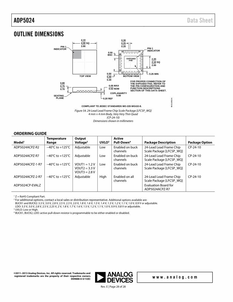
OUTLINE DIMENSIONS
0.50BSC
0.500.400.30
0.300.250.20
COMPLIANT TO JEDEC STANDARDS MO-220-WGGD-8. 06-1
1-20
12-A
BOTTOM VIEWTOP VIEW
EXPOSEDPAD
PIN 1INDICATOR
4.104.00 SQ3.90
SEATINGPLANE
0.800.750.70
0.20 REF
0.25 MIN
COPLANARITY0.08
PIN 1INDICATOR
2.202.10 SQ2.00
124
71213
1819
6
FOR PROPER CONNECTION OFTHE EXPOSED PAD, REFER TOTHE PIN CONFIGURATION ANDFUNCTION DESCRIPTIONSSECTION OF THIS DATA SHEET.
0.05 MAX0.02 NOM
Figure 54. 24-Lead Lead Frame Chip Scale Package [LFCSP_WQ]
4 mm × 4 mm Body, Very Very Thin Quad (CP-24-10)
Dimensions shown in millimeters
ORDERING GUIDE
Model1 Temperature Range
Output Voltage2 UVLO3
Active Pull-Down4 Package Description Package Option
ADP5024ACPZ-R2 −40°C to +125°C Adjustable Low Enabled on buck channels
24-Lead Lead Frame Chip Scale Package [LFCSP_WQ]
CP-24-10
ADP5024ACPZ-R7 −40°C to +125°C Adjustable Low Enabled on buck channels
24-Lead Lead Frame Chip Scale Package [LFCSP_WQ]
CP-24-10
ADP5024ACPZ-1-R7 −40°C to +125°C VOUT1 = 1.2 VVOUT2 = 3.3 VVOUT3 = 2.8 V
Low Enabled on buck channels
24-Lead Lead Frame Chip Scale Package [LFCSP_WQ]
CP-24-10
ADP5024ACPZ-2-R7 −40°C to +125°C Adjustable High Enabled on all channels
24-Lead Lead Frame Chip Scale Package [LFCSP_WQ]
CP-24-10
ADP5024CP-EVALZ Evaluation Board for ADP5024ACPZ-R7
1 Z = RoHS Compliant Part. 2 For additional options, contact a local sales or distribution representative. Additional options available are:
BUCK1 and BUCK2: 3.3 V, 3.0 V, 2.8 V, 2.5 V, 2.3 V, 2.0 V, 1.8 V, 1.6 V, 1.5 V, 1.4 V, 1.3 V, 1.2 V, 1.1 V, 1.0 V, 0.9 V or adjustable. LDO: 3.3 V, 3.0 V, 2.8 V, 2.5 V, 2.25 V, 2 V, 1.8 V, 1.7 V, 1.6 V, 1.5 V, 1.2 V, 1.1 V, 1.0 V, 0.9 V, 0.8 V or adjustable.
3 UVLO: Low or High. 4 BUCK1, BUCK2, LDO: active pull-down resistor is programmable to be either enabled or disabled.
©2011–2013 Analog Devices, Inc. All rights reserved. Trademarks and registered trademarks are the property of their respective owners. D09888-0-5/13(E)