DUAL 2:1 AND 1:2, ICS85354 DIFFERENTIAL-TO-LVPECL/ECL ... Sheets/IDT/ICS85354.pdf ·...
19
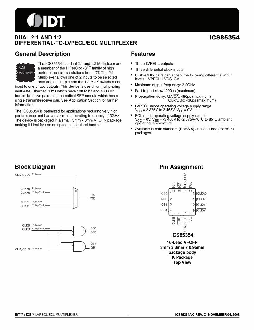
DUAL 2:1 AND 1:2, DIFFERENTIAL-TO-LVPECL/ECL MULTIPLEXER ICS85354 IDT™ / ICS™ LVPECL/ECL MULTIPLEXER 1 ICS85354AK REV. C NOVEMBER 04, 2008 General Description The ICS85354 is a dual 2:1 and 1:2 Multiplexer and a member of the HiPerClockS TM family of high performance clock solutions from IDT. The 2:1 Multiplexer allows one of 2 inputs to be selected onto one output pin and the 1:2 MUX switches one input to one of two outputs. This device is useful for multiplexing multi-rate Ethernet PHYs which have 100 M bit and 1000 bit transmit/receive pairs onto an optical SFP module which has a single transmit/receive pair. See Application Section for further information. The ICS85354 is optimized for applications requiring very high performance and has a maximum operating frequency of 3GHz. The device is packaged in a small, 3mm x 3mm VFQFN package, making it ideal for use on space-constrained boards. Features • Three LVPECL outputs • Three differential clock inputs • CLKx/CLKx pairs can accept the following differential input levels: LVPECL, LVDS, CML • Maximum output frequency: 3.2GHz • Part-to-part skew: 200ps (maximum) • Propagation delay: QA/QA : 450ps (maximum) QBx/QBx : 430ps (maximum) • LVPECL mode operating voltage supply range: V CC = 2.375V to 3.465V, V EE = 0V • ECL mode operating voltage supply range: V CC = 0V, V EE = -3.465V to -2.375V-40°C to 85°C ambient operating temperature • Available in both standard (RoHS 5) and lead-free (RoHS 6) packages HiPerClockS™ ICS 0 1 QA QA CLKA0 CLK_SELA CLK_SELB CLKA0 CLKA1 CLKA1 CLKB CLKB QB0 QB0 QB1 QB1 Pulldown Pulldown Pulldown Pulldown Pulldown Pullup/Pulldown Pullup/Pulldown Pullup/Pulldown 5 6 7 8 16 15 14 13 1 2 3 4 12 11 10 9 QB0 QB0 QB1 QB1 CLKA0 CLKA0 CLKA1 CLKA1 CLKB CLKB CLK_SELB VEE QA CLK_SELA VCC QA ICS85354 16-Lead VFQFN 3mm x 3mm x 0.95mm package body K Package Top View Pin Assignment Block Diagram
-
Upload
nguyenmien -
Category
Documents
-
view
219 -
download
0
Transcript of DUAL 2:1 AND 1:2, ICS85354 DIFFERENTIAL-TO-LVPECL/ECL ... Sheets/IDT/ICS85354.pdf ·...
DUAL 2:1 AND 1:2, DIFFERENTIAL-TO-LVPECL/ECL MULTIPLEXER
ICS85354
IDT™ / ICS™ LVPECL/ECL MULTIPLEXER 1 ICS85354AK REV. C NOVEMBER 04, 2008
General Description
The ICS85354 is a dual 2:1 and 1:2 Multiplexer and a member of the HiPerClockSTM family of high performance clock solutions from IDT. The 2:1 Multiplexer allows one of 2 inputs to be selected onto one output pin and the 1:2 MUX switches one
input to one of two outputs. This device is useful for multiplexing multi-rate Ethernet PHYs which have 100 M bit and 1000 bit transmit/receive pairs onto an optical SFP module which has a single transmit/receive pair. See Application Section for further information.
The ICS85354 is optimized for applications requiring very high performance and has a maximum operating frequency of 3GHz. The device is packaged in a small, 3mm x 3mm VFQFN package, making it ideal for use on space-constrained boards.
Features
• Three LVPECL outputs
• Three differential clock inputs
• CLKx/CLKx pairs can accept the following differential input levels: LVPECL, LVDS, CML
• Maximum output frequency: 3.2GHz
• Part-to-part skew: 200ps (maximum)
• Propagation delay: QA/QA: 450ps (maximum) QBx/QBx: 430ps (maximum)
• LVPECL mode operating voltage supply range:VCC = 2.375V to 3.465V, VEE = 0V
• ECL mode operating voltage supply range:VCC = 0V, VEE = -3.465V to -2.375V-40°C to 85°C ambient operating temperature
• Available in both standard (RoHS 5) and lead-free (RoHS 6) packages
HiPerClockS™
ICS
0
1
QAQA
CLKA0
CLK_SELA
CLK_SELB
CLKA0
CLKA1CLKA1
CLKBCLKB QB0
QB0
QB1QB1
Pulldown
Pulldown
Pulldown
Pulldown
Pulldown
Pullup/Pulldown
Pullup/Pulldown
Pullup/Pulldown
5 6 7 8
16 15 14 13 1
2
3
4
12
11
10
9
QB0
QB0
QB1
QB1
CLKA0
CLKA0
CLKA1
CLKA1
CLK
B
CLK
B
CLK
_SE
LB VE
E
QA
CLK
_SE
L A
VC
C
QA
ICS8535416-Lead VFQFN
3mm x 3mm x 0.95mm package body
K PackageTop View
Pin AssignmentBlock Diagram

ICS85354DUAL 2:1 AND 1:2, DIFFERENTIAL-TO-LVPECL/ECL MULTIPLEXER
IDT™ / ICS™ LVPECL/ECL MULTIPLEXER 2 ICS85354AK REV. C NOVEMBER 04, 2008
Table 1. Pin Descriptions
NOTE: Pullup and Pulldown refer to internal input resistors. See Table 2, Pin Characteristics, for typical values.
Table 2. Pin Characteristics
Function TablesTable 3A. Control Input Function Table, (Bank A) Table 3B. Control Input Function Table, (Bank B)
Number Name Type Description
1, 2 QB0/QB0 Output Differential output pair. LVPECL/ECL interface levels.
3, 4 QB1/QB1 Output Differential output pair. LVPECL/ECL interface levels.
5 CLKB Input Pulldown Non-inverting LVPECL/ECL differential clock input.
6 CLKB InputPullup/
PulldownInverting differential LVPECL clock input. VCC/2 default when left floating.
7 CLK_SELB Input PulldownClock select pin for QBx outputs. When HIGH, selects QB1/QB1 outputs. When LOW, selects QB0/QB0 outputs. LVCMOS/LVTTL interface levels.
8 VEE Power Negative supply pin.
9 CLKA1 InputPullup/
PulldownInverting differential LVPECL clock input. VCC/2 default when left floating.
10 CLKA1 Input Pulldown Non-inverting LVPECL/ECL differential clock input.
11 CLKA0 InputPullup/
PulldownInverting differential LVPECL clock input. VCC/2 default when left floating.
12 CLKA0 Input Pulldown Non-inverting LVPECL/ECL differential clock input.
13 VCC Power Positive supply pin.
14 CLK_SELA Input PulldownClock select pin for QA output. When HIGH, selects QA output. When LOW, selects QA output. LVCMOS/LVTTL interface levels.
15, 16 QA/QA Output Differential output pair. LVPECL/ECL interface levels.
Symbol Parameter Test Conditions Minimum Typical Maximum Units
RPULLDOWN Input Pulldown Resistor 37.5 kΩ
RVCC/2 Pullup/Pulldown Resistor 37.5 kΩ
Bank A
Control Input Outputs
CLK_SELA QA/QA
0 Selects CLKA0/CLKA0
1 Selects CLKA1/CLKA1
Bank B
Control Input Outputs
CLK_SELB QB0/QB0 QB1/QB1
0 Follows CLKB input Low
1 Low Follows CLKB input

ICS85354DUAL 2:1 AND 1:2, DIFFERENTIAL-TO-LVPECL/ECL MULTIPLEXER
IDT™ / ICS™ LVPECL/ECL MULTIPLEXER 3 ICS85354AK REV. C NOVEMBER 04, 2008
Absolute Maximum RatingsNOTE: Stresses beyond those listed under Absolute Maximum Ratings may cause permanent damage to the device. These ratings are stress specifications only. Functional operation of product at these conditions or any conditions beyond those listed in the DC Characteristics or AC Characteristics is not implied. Exposure to absolute maximum rating conditions for extended periods may affect product reliability.
DC Electrical CharacteristicsTable 4A. Power Supply DC Characteristics, VCC = 2.375V to 3.465V, VEE = 0V or VCC = 0V, VEE = -3.465V to -2.375V, TA = -40°C to 85°C
Table 4B. LVCMOS/LVTTL DC Characteristics, VCC = 2.375V to 3.465V, VEE = 0V, TA = -40°C to 85°C
Item Rating
Supply Voltage, VCC 4.6V (LVPECL mode, VEE = 0V)
Negative Supply Voltage, VEE -4.6V (ECL mode, VCC = 0V)
Inputs, VI (LVPECL mode) -0.5V to VCC + 0.5V
Inputs, VI (ECL mode) 0.5V to VEE – 0.5V
Outputs, IO Continuos CurrentSurge Current
50mA100mA
Operating Termperature Range, TA -40°C to 85°C
Storage Temperature, TSTG -65°C to 150°C
Package Thermal Impedance, θJA 51.5°C/W (0 lfpm)
Symbol Parameter Test Conditions Minimum Typical Maximum Units
VCC Positive Supply Voltage3.135 3.3 3.465 V
2.375 2.5 2.625 V
IEE Power Supply Current 50 mA
Symbol Parameter Test Conditions Minimum Typical Maximum Units
VIH Input High Voltage 0.7VCC VCC + 0.3 V
VIL Input Low Voltage -0.3 0.3VCC V
IIH Input High CurrentCLK_SELA, CLK_SELB
VCC = VIN 150 µA
IIL Input Low CurrentCLK_SELA, CLK_SELB
VCC = VIN -150 µA
ICS85354DUAL 2:1 AND 1:2, DIFFERENTIAL-TO-LVPECL/ECL MULTIPLEXER
IDT™ / ICS™ LVPECL/ECL MULTIPLEXER 4 ICS85354AK REV. C NOVEMBER 04, 2008
Table 4C. LVCMOS/LVTTL DC Characteristics, VCC = 0V, VEE = -3.465V to -2.375V, TA = -40°C to 85°C
Table 4D. LVPECL DC Characteristics, VCC = 2.375V to 3.465V, VEE = 0V, TA = -40°C to 85°C
NOTE 1: Common mode input voltage is defined as VIH.NOTE 2: For single-ended applications, the maximum input voltage for CLKx, CLKx is VCC + 0.3V.NOTE 3: Outputs terminated with 50Ω to VCC – 2V.
Symbol Parameter Test Conditions Minimum Typical Maximum Units
VIH Input High Voltage 0.3VEE 0.3 V
VIL Input Low Voltage VEE – 0.3 0.7VEE V
IIH Input High CurrentCLK_SELA, CLK_SELB
VCC = VIN 150 µA
IIL Input Low CurrentCLK_SELA, CLK_SELB
VCC = VIN -150 µA
Symbol Parameter Test Conditions Minimum Typical Maximum Units
IIH Input High CurrentCLKA[0:1], CLKB VCC = VIN 200 µA
CLKA[0:1], CLKB VCC = VIN 200 µA
IIL Input Low Current
CLKA[0:1], CLKBVCC = 3.465V,
VIN = 0V-200 µA
CLKA[0:1], CLKB VCC = 3.465V,
VIN = 0V-200 µA
VPP Peak-to-Peak Input Voltage 0.15 1.2 V
VCMRCommon Mode Input Voltage; NOTE 1, 2
1.2 VCC V
VOH Output High Current; NOTE 3 VCC – 1.125 VCC – 1.005 VCC – 0.92 V
VOL Output Low Current; NOTE 3 VCC – 1.895 VCC – 1.78 VCC – 1.62 V
VSWING Peak-to-Peak Output Voltage Swing 0.6 1.0 V

ICS85354DUAL 2:1 AND 1:2, DIFFERENTIAL-TO-LVPECL/ECL MULTIPLEXER
IDT™ / ICS™ LVPECL/ECL MULTIPLEXER 5 ICS85354AK REV. C NOVEMBER 04, 2008
AC Electrical CharacteristicsTable 5. AC Characteristics, VCC = 2.375V to 3.465V, VEE = 0V or VCC = 0V, VEE = -3.465V to -2.375V, TA = -40°C to 85°C
All parameters are measured ≤ 1GHz unless otherwise noted.NOTE 1: Measured from the differential input crossing point to the differential output crossing point.NOTE 2: Defined as skew between outputs on different devices operating at the same supply voltages and with equal load conditions. Using the same type of inputs on each device, the outputs are measured at the differential cross points.NOTE 3: This parameter is defined in accordance with JEDEC Standard 65.NOTE 4: Measured using standard LVPECL input at 622MHz.
Parameter Symbol Test Conditions Minimum Typical Maximum Units
fMAX Output Frequency 3.2 GHz
tPDPropagation Delay; NOTE 1
QA/QA 225 335 445 ps
QBx/QBx 195 305 420 ps
tsk(pp) Part-to-Part Skew; NOTE 2, 3 200 ps
MUX_ISOLATION MUX Isolation; NOTE 4 55 dB
tR / tF Output Rise/Fall Time 20% to 80% 75 155 245 ps

ICS85354DUAL 2:1 AND 1:2, DIFFERENTIAL-TO-LVPECL/ECL MULTIPLEXER
IDT™ / ICS™ LVPECL/ECL MULTIPLEXER 6 ICS85354AK REV. C NOVEMBER 04, 2008
Parameter Measurement Information
LVPECL Output Load AC Test Circuit
Part-to-Part Skew
Output Rise/Fall Time
Differential Input Level
Propagation Delay
SCOPEQx
nQxLVPECL
VEE
VCC
2V
-0.375V to -1.465V
tsk(pp)
Par t 1
Par t 2
Qx
Qx
Qx
Qx
Clock Outputs
20%
80% 80%
20%
tR tF
VSWING
VCMR
Cross Points VPP
VCC
VEE
CLKA0, CLKA1,CLKB
CLKA0, CLKA1,CLKB
tPD
CLKA[0:1],CLKB
CLKA[0:1],CLKB
QA,QB[0:1]
QA,QB[0:1]

ICS85354DUAL 2:1 AND 1:2, DIFFERENTIAL-TO-LVPECL/ECL MULTIPLEXER
IDT™ / ICS™ LVPECL/ECL MULTIPLEXER 7 ICS85354AK REV. C NOVEMBER 04, 2008
Application Information
Wiring the Differential Input to Accept Single Ended Levels
Figure 1 shows how the differential input can be wired to accept single ended levels. The reference voltage V_REF = VCC/2 is generated by the bias resistors R1, R2 and C1. This bias circuit should be located as close as possible to the input pin. The ratio of R1 and R2 might need to be adjusted to position the V_REF in the center of the input voltage swing. For example, if the input clock swing is only 2.5V and VCC = 3.3V, V_REF should be 1.25V and R2/R1 = 0.609.
Figure 1. Single-Ended Signal Driving Differential Input
Recommendations for Unused Input and Output Pins
Inputs:
LVCMOS Control PinsAll control pins have internal pull-ups or pull-downs; additional resistance is not required but can be added for additional protection. A 1kΩ resistor can be used.
CLK/CLK INPUTS
For applications not requiring the use of the differential input, both CLK and CLK can be left floating. Though not required, but for additional protection, a 1kΩ resistor can be tied from CLK to ground.
Outputs:
LVPECL OutputsAll unused LVPECL outputs can be left floating. We recommend that there is no trace attached. Both sides of the differential output pair should either be left floating or terminated.
V_REF
Single Ended Clock Input
VCC
CLKx
nCLKx
R11K
C10.1u R2
1K
ICS85354DUAL 2:1 AND 1:2, DIFFERENTIAL-TO-LVPECL/ECL MULTIPLEXER
IDT™ / ICS™ LVPECL/ECL MULTIPLEXER 8 ICS85354AK REV. C NOVEMBER 04, 2008
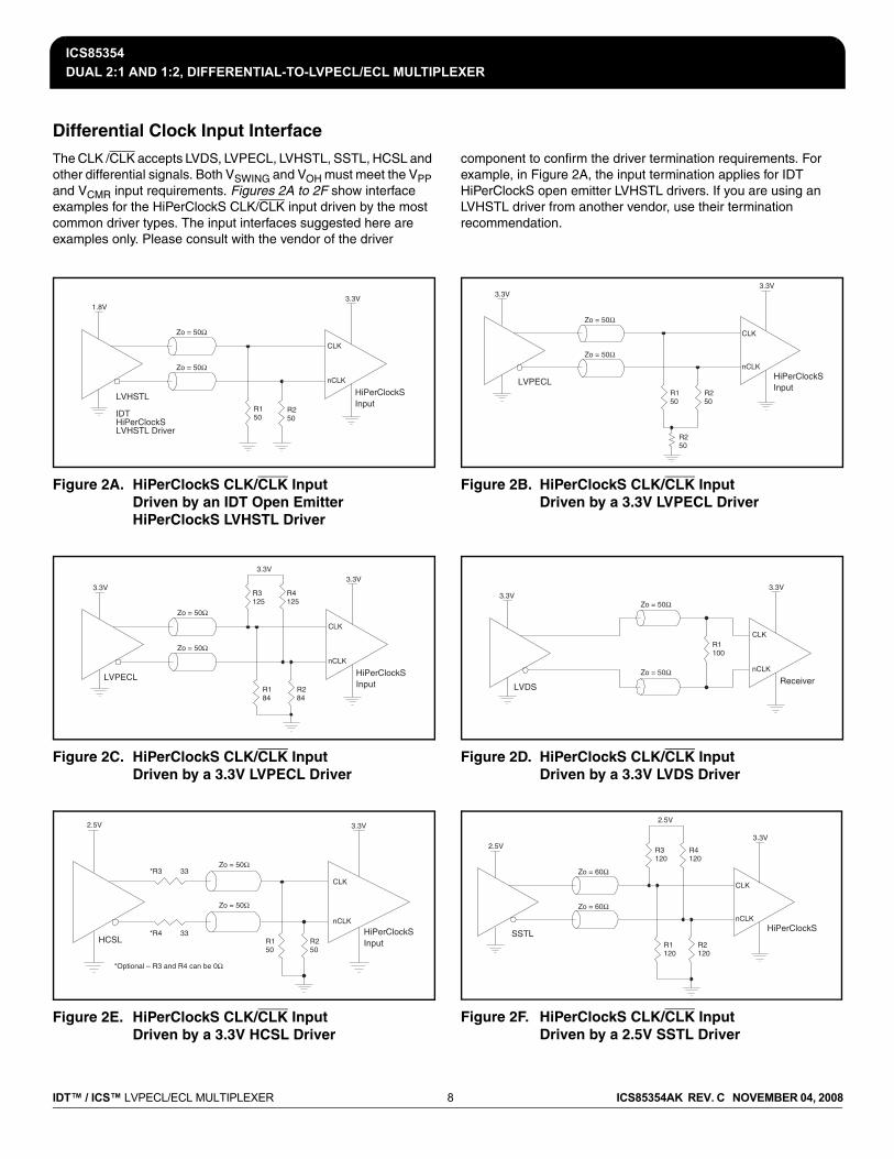
Differential Clock Input Interface
The CLK /CLK accepts LVDS, LVPECL, LVHSTL, SSTL, HCSL and other differential signals. Both VSWING and VOH must meet the VPP and VCMR input requirements. Figures 2A to 2F show interface examples for the HiPerClockS CLK/CLK input driven by the most common driver types. The input interfaces suggested here are examples only. Please consult with the vendor of the driver
component to confirm the driver termination requirements. For example, in Figure 2A, the input termination applies for IDT HiPerClockS open emitter LVHSTL drivers. If you are using an LVHSTL driver from another vendor, use their termination recommendation.
Figure 2A. HiPerClockS CLK/CLK Input Driven by an IDT Open Emitter HiPerClockS LVHSTL Driver
Figure 2C. HiPerClockS CLK/CLK InputDriven by a 3.3V LVPECL Driver
Figure 2E. HiPerClockS CLK/CLK InputDriven by a 3.3V HCSL Driver
Figure 2B. HiPerClockS CLK/CLK Input Driven by a 3.3V LVPECL Driver
Figure 2D. HiPerClockS CLK/CLK InputDriven by a 3.3V LVDS Driver
Figure 2F. HiPerClockS CLK/CLK InputDriven by a 2.5V SSTL Driver
R150
R250
1.8V
Zo = 50Ω
Zo = 50Ω
CLK
nCLK
3.3V
LVHSTL
IDTHiPerClockS LVHSTL Driver
HiPerClockSInput
R3125
R4125
R184
R284
3.3V
Zo = 50Ω
Zo = 50Ω
CLK
nCLK
3.3V3.3V
LVPECL HiPerClockSInput
HCSL
*R3 33
*R4 33
CLK
nCLK
2.5V 3.3V
Zo = 50Ω
Zo = 50Ω
HiPerClockSInputR1
50R250
*Optional – R3 and R4 can be 0Ω
CLK
nCLKHiPerClockS Input
LVPECL
3.3V
Zo = 50Ω
Zo = 50Ω
3.3V
R150
R250
R250
3.3V
R1100
LVDS
CLK
nCLK
3.3V
Receiver
Zo = 50Ω
Zo = 50Ω
CLK
nCLKHiPerClockS
SSTL
2.5V
Zo = 60Ω
Zo = 60Ω
2.5V
3.3V
R1120
R2120
R3120
R4120
ICS85354DUAL 2:1 AND 1:2, DIFFERENTIAL-TO-LVPECL/ECL MULTIPLEXER
IDT™ / ICS™ LVPECL/ECL MULTIPLEXER 9 ICS85354AK REV. C NOVEMBER 04, 2008
VFQFN EPAD Thermal Release Path
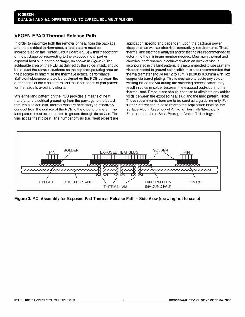
In order to maximize both the removal of heat from the package and the electrical performance, a land pattern must be incorporated on the Printed Circuit Board (PCB) within the footprint of the package corresponding to the exposed metal pad or exposed heat slug on the package, as shown in Figure 3. The solderable area on the PCB, as defined by the solder mask, should be at least the same size/shape as the exposed pad/slug area on the package to maximize the thermal/electrical performance. Sufficient clearance should be designed on the PCB between the outer edges of the land pattern and the inner edges of pad pattern for the leads to avoid any shorts.
While the land pattern on the PCB provides a means of heat transfer and electrical grounding from the package to the board through a solder joint, thermal vias are necessary to effectively conduct from the surface of the PCB to the ground plane(s). The land pattern must be connected to ground through these vias. The vias act as “heat pipes”. The number of vias (i.e. “heat pipes”) are
application specific and dependent upon the package power dissipation as well as electrical conductivity requirements. Thus, thermal and electrical analysis and/or testing are recommended to determine the minimum number needed. Maximum thermal and electrical performance is achieved when an array of vias is incorporated in the land pattern. It is recommended to use as many vias connected to ground as possible. It is also recommended that the via diameter should be 12 to 13mils (0.30 to 0.33mm) with 1oz copper via barrel plating. This is desirable to avoid any solder wicking inside the via during the soldering process which may result in voids in solder between the exposed pad/slug and the thermal land. Precautions should be taken to eliminate any solder voids between the exposed heat slug and the land pattern. Note: These recommendations are to be used as a guideline only. For further information, please refer to the Application Note on the Surface Mount Assembly of Amkor’s Thermally/Electrically Enhance Leadfame Base Package, Amkor Technology.
Figure 3. P.C. Assembly for Exposed Pad Thermal Release Path – Side View (drawing not to scale)
SOLDERSOLDER PINPIN EXPOSED HEAT SLUG
PIN PAD PIN PADGROUND PLANE LAND PATTERN (GROUND PAD)THERMAL VIA

ICS85354DUAL 2:1 AND 1:2, DIFFERENTIAL-TO-LVPECL/ECL MULTIPLEXER
IDT™ / ICS™ LVPECL/ECL MULTIPLEXER 10 ICS85354AK REV. C NOVEMBER 04, 2008
Termination for 3.3V LVPECL Outputs
The clock layout topology shown below is a typical termination for LVPECL outputs. The two different layouts mentioned are recommended only as guidelines.
FOUT and FOUT are low impedance follower outputs that generate ECL/LVPECL compatible outputs. Therefore, terminating resistors (DC current path to ground) or current sources must be used for functionality. These outputs are designed to drive 50Ω
transmission lines. Matched impedance techniques should be used to maximize operating frequency and minimize signal distortion. Figures 4A and 4B show two different layouts which are recommended only as guidelines. Other suitable clock layouts may exist and it would be recommended that the board designers simulate to guarantee compatibility across all printed circuit and clock component process variations.
Figure 4A. 3.3V LVPECL Output Termination Figure 4B. 3.3V LVPECL Output Termination
VCC - 2V
50Ω 50Ω
RTT
Zo = 50Ω
Zo = 50Ω
FOUT FIN
RTT = Zo 1((VOH + VOL) / (VCC – 2)) – 2
3.3V
125Ω 125Ω
84Ω 84Ω
Zo = 50Ω
Zo = 50Ω
FOUT FIN

ICS85354DUAL 2:1 AND 1:2, DIFFERENTIAL-TO-LVPECL/ECL MULTIPLEXER
IDT™ / ICS™ LVPECL/ECL MULTIPLEXER 11 ICS85354AK REV. C NOVEMBER 04, 2008
Termination for 2.5V LVPECL Outputs
Figure 5A and Figure 5B show examples of termination for 2.5V LVPECL driver. These terminations are equivalent to terminating 50Ω to VCC – 2V. For VCC = 2.5V, the VCC – 2V is very close to
ground level. The R3 in Figure 5B can be eliminated and the termination is shown in Figure 5C.
Figure 5A. 2.5V LVPECL Driver Termination Example
Figure 5C. 2.5V LVPECL Driver Termination Example
Figure 5B. 2.5V LVPECL Driver Termination Example
2.5V LVPECL Driver
VCC = 2.5V2.5V
2.5V
50Ω
50Ω
R1250
R3250
R262.5
R462.5
+
–
2.5V LVPECL Driver
VCC = 2.5V2.5V
50Ω
50Ω
R150
R250
+
–
2.5V LVPECL Driver
VCC = 2.5V2.5V
50Ω
50Ω
R150
R250
R318
+
–

ICS85354DUAL 2:1 AND 1:2, DIFFERENTIAL-TO-LVPECL/ECL MULTIPLEXER
IDT™ / ICS™ LVPECL/ECL MULTIPLEXER 12 ICS85354AK REV. C NOVEMBER 04, 2008
A Typical Application for the ICS85354
Used to connect a multi-rate PHY with the Tx/Rx pins of an SFP Module.
Problem Addressed: How to map the 2 Tx/Rx pairs of the multi-rate PHY to the single Tx/Rx pair on the SFP Module.
Mode 1, 100BaseX Connected to SFP
All lines are differential pairs, but drawn as single-ended to simplify the drawing.
Bold red lines are active connections highlighting the signal path.
MULTI-RATE PHY SFP MODULE
100BaseFX
1000BaseX
Tx
Rx
RxRx
TxTx ?
MULTI-RATE PHY SFP MODULE
100BaseFX
1000BaseX
Tx
Rx
Tx
Rx
Rx
Tx
0
1
ICS85354
CLK_SELA = 0
CLKA1
QB0
QB1
CLKA0
CLK_SELB = 0
QA
CLKB

ICS85354DUAL 2:1 AND 1:2, DIFFERENTIAL-TO-LVPECL/ECL MULTIPLEXER
IDT™ / ICS™ LVPECL/ECL MULTIPLEXER 13 ICS85354AK REV. C NOVEMBER 04, 2008
Mode 2, 100BaseX Connected to SFP
All lines are differential pairs, but drawn as single-ended to simplify the drawing.
Bold red lines are active connections highlighting the signal path.
MULTI-RATE PHY SFP MODULE
100BaseFX
1000BaseX
Tx
Rx
Tx
Rx
Rx
Tx
0
1
ICS85354
CLK_SELA = 1
CLKA1
QB0
QB1
CLKA0
CLK_SELB = 1
QA
CLKB
ICS85354DUAL 2:1 AND 1:2, DIFFERENTIAL-TO-LVPECL/ECL MULTIPLEXER
IDT™ / ICS™ LVPECL/ECL MULTIPLEXER 14 ICS85354AK REV. C NOVEMBER 04, 2008
Power ConsiderationsThis section provides information on power dissipation and junction temperature for the ICS85354. Equations and example calculations are also provided.
1. Power Dissipation.
The total power dissipation for the ICS85354 is the sum of the core power plus the power dissipated in the load(s). The following is the power dissipation for VCC = 3.3V + 5% = 3.465V, which gives worst case results.
NOTE: Please refer to Section 3 for details on calculating power dissipated in the load.
• Power (core)MAX = VCC_MAX * IEE_MAX = 3.465V * 50mA = 173.25mW
• Power (outputs)MAX = 27.83mW/Loaded Output pairIf all outputs are loaded, the total power is 4 * 27.83mW = 111.3mW
Total Power_MAX (3.3V, with all outputs switching) =173.25mW + 111.3mW = 284.55mW
2. Junction Temperature.
Junction temperature, Tj, is the temperature at the junction of the bond wire and bond pad and directly affects the reliability of the device. The maximum recommended junction temperature for HiPerClockS devices is 125°C.
The equation for Tj is as follows: Tj = θJA * Pd_total + TA
Tj = Junction Temperature
θJA = Junction-to-Ambient Thermal Resistance
Pd_total = Total Device Power Dissipation (example calculation is in section 1 above)
TA = Ambient Temperature
In order to calculate junction temperature, the appropriate junction-to-ambient thermal resistance θJA must be used. Assuming a moderate air flow of 1 meter per second and a multi-layer board, the appropriate value is 65°C/W per Table 6 below.
Therefore, Tj for an ambient temperature of 85°C with all outputs switching is:
85°C + 0.285W * 51.5°C/W = 99.7°C. This is well below the limit of 125°C.
This calculation is only an example. Tj will obviously vary depending on the number of loaded outputs, supply voltage, air flow and the type of board (single layer or multi-layer).
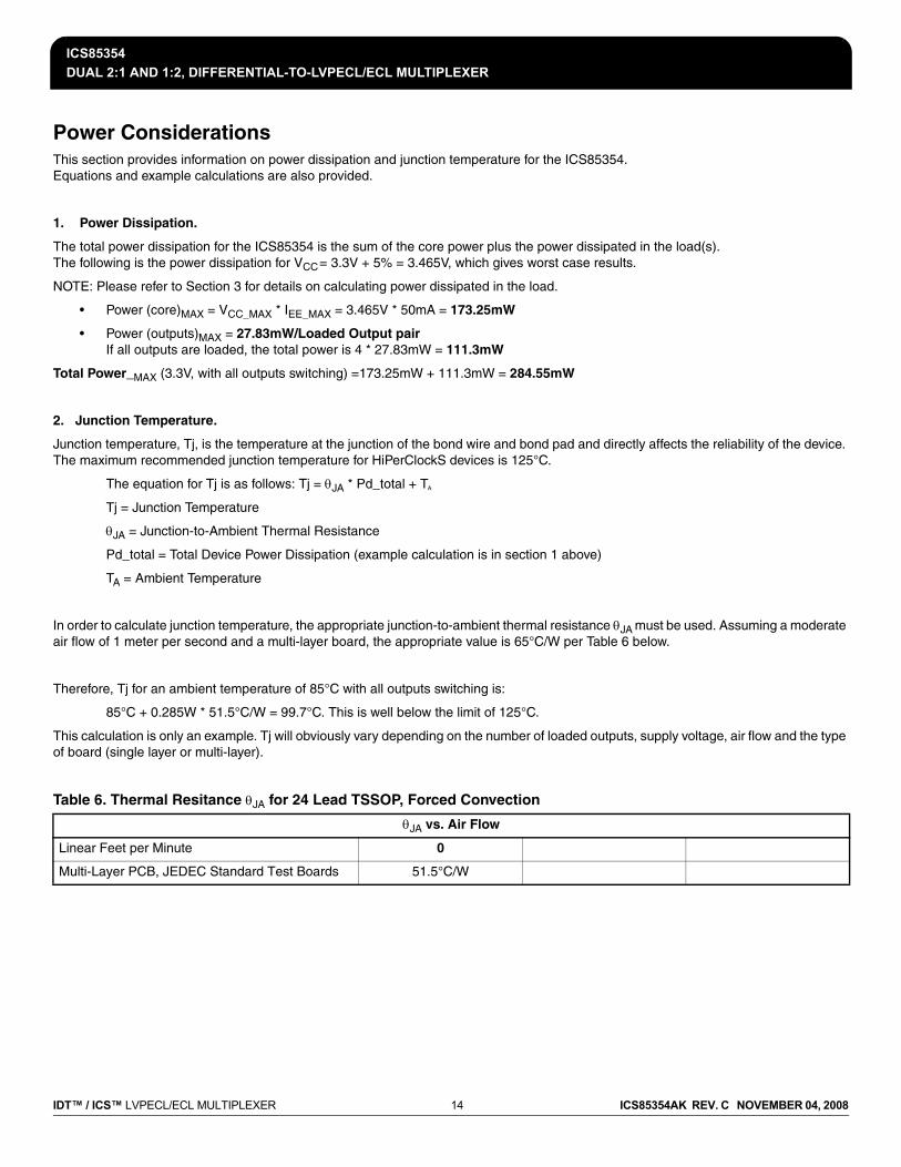
Table 6. Thermal Resitance θJA for 24 Lead TSSOP, Forced Convection
θJA vs. Air Flow
Linear Feet per Minute 0
Multi-Layer PCB, JEDEC Standard Test Boards 51.5°C/W
ICS85354DUAL 2:1 AND 1:2, DIFFERENTIAL-TO-LVPECL/ECL MULTIPLEXER
IDT™ / ICS™ LVPECL/ECL MULTIPLEXER 15 ICS85354AK REV. C NOVEMBER 04, 2008
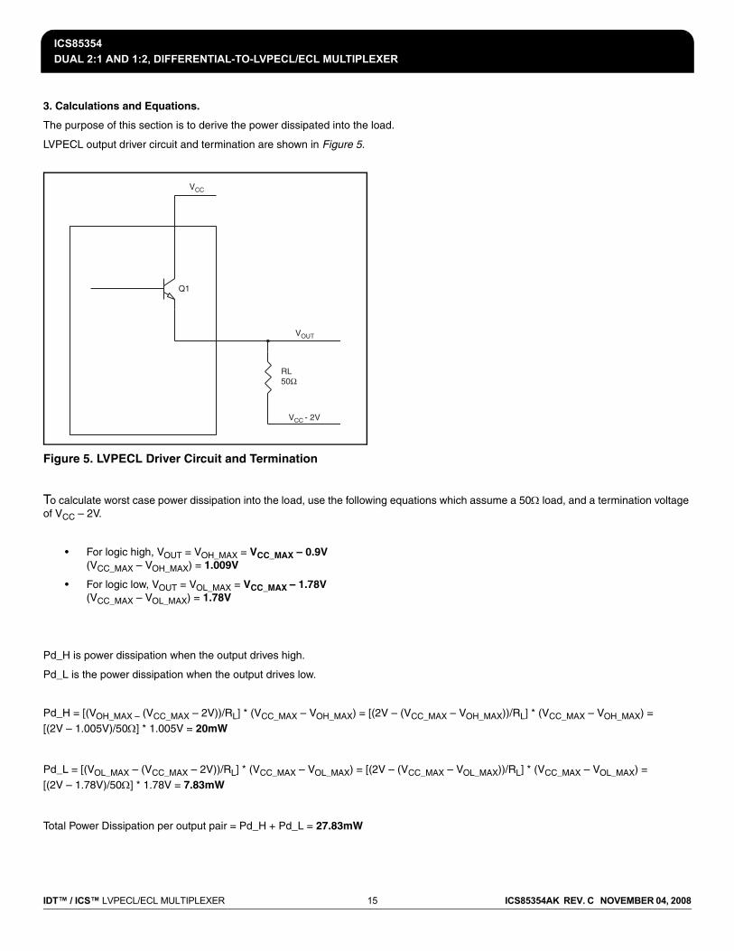
3. Calculations and Equations.
The purpose of this section is to derive the power dissipated into the load.
LVPECL output driver circuit and termination are shown in Figure 5.
Figure 5. LVPECL Driver Circuit and Termination
To calculate worst case power dissipation into the load, use the following equations which assume a 50Ω load, and a termination voltage of VCC – 2V.
• For logic high, VOUT = VOH_MAX = VCC_MAX – 0.9V(VCC_MAX – VOH_MAX) = 1.009V
• For logic low, VOUT = VOL_MAX = VCC_MAX – 1.78V(VCC_MAX – VOL_MAX) = 1.78V
Pd_H is power dissipation when the output drives high.
Pd_L is the power dissipation when the output drives low.
Pd_H = [(VOH_MAX – (VCC_MAX – 2V))/RL] * (VCC_MAX – VOH_MAX) = [(2V – (VCC_MAX – VOH_MAX))/RL] * (VCC_MAX – VOH_MAX) =
[(2V – 1.005V)/50Ω] * 1.005V = 20mW
Pd_L = [(VOL_MAX – (VCC_MAX – 2V))/RL] * (VCC_MAX – VOL_MAX) = [(2V – (VCC_MAX – VOL_MAX))/RL] * (VCC_MAX – VOL_MAX) =
[(2V – 1.78V)/50Ω] * 1.78V = 7.83mW
Total Power Dissipation per output pair = Pd_H + Pd_L = 27.83mW
VOUT
VCC
VCC - 2V
Q1
RL50Ω
ICS85354DUAL 2:1 AND 1:2, DIFFERENTIAL-TO-LVPECL/ECL MULTIPLEXER
IDT™ / ICS™ LVPECL/ECL MULTIPLEXER 16 ICS85354AK REV. C NOVEMBER 04, 2008
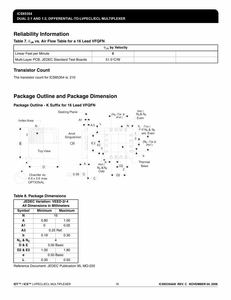
Reliability InformationTable 7. θJA vs. Air Flow Table for a 16 Lead VFQFN
Transistor Count
The transistor count for ICS85354 is: 210
Package Outline and Package Dimension
Package Outline - K Suffix for 16 Lead VFQFN
Table 8. Package Dimensions
Reference Document: JEDEC Publication 95, MO-220
θJA by Velocity
Linear Feet per Minute 0
Multi-Layer PCB, JEDEC Standard Test Boards 51.5°C/W
JEDEC Variation: VEED-2/-4All Dimensions in Millimeters
Symbol Minimum MaximumN 16
A 0.80 1.00
A1 0 0.05A3 0.25 Ref.
b 0.18 0.30
ND & NE 4D & E 3.00 Basic
D2 & E2 1.00 1.80
e 0.50 Basic
L 0.30 0.50
Top View
Index Area
D
Chamfer 4x0.6 x 0.6 maxOPTIONAL
AnvilSingula tion
A
0. 08 CC
A3
A1
Seating Plane
E2E2 2
L
(N -1)x e (Ref.)
(Ref.)N & N Even
N
eD2 2
D2
(Ref.)N & N Odd
1
2
e2
(Typ.)If N & N are Even
(N -1)x e (Re f.)
b
Thermal Base
N
OR
D E
D D E
D E
E

ICS85354DUAL 2:1 AND 1:2, DIFFERENTIAL-TO-LVPECL/ECL MULTIPLEXER
IDT™ / ICS™ LVPECL/ECL MULTIPLEXER 17 ICS85354AK REV. C NOVEMBER 04, 2008
Ordering InformationTable 9. Ordering Information
NOTE: Parts that are ordered with an "LF" suffix to the part number are the Pb-Free configuration and are RoHS compliant.
Part/Order Number Marking Package Shipping Packaging Temperature85354AK 354A 16 Lead VFQFN Tube -40°C to 85°C85354AKT 354A 16 Lead VFQFN 2500 Tape & Reel -40°C to 85°C85354AKLF 54AL “Lead-Free” 16 Lead VFQFN Tube -40°C to 85°C85354AKLFT 54AL “Lead-Free” 16 Lead VFQFN 2500 Tape & Reel -40°C to 85°C
While the information presented herein has been checked for both accuracy and reliability, Integrated Device Technology (IDT) assumes no responsibility for either its use or for the infringement of any patents or other rights of third parties, which would result from its use. No other circuits, patents, or licenses are implied. This product is intended for use in normal commercial and industrial applications. Any other applications, such as those requiring high reliability or other extraordinary environmental requirements are not recommended without additional processing by IDT. IDT reserves the right to change any circuitry or specifications without notice. IDT does not authorize or warrant any IDT product for use in life support devices or critical medical instruments.

ICS85354DUAL 2:1 AND 1:2, DIFFERENTIAL-TO-LVPECL/ECL MULTIPLEXER
IDT™ / ICS™ LVPECL/ECL MULTIPLEXER 18 ICS85354AK REV. C NOVEMBER 04, 2008
Revision History Sheet
Rev Table Page Description of Change Date
B T4D 4 LVPECL Characteristics Table - added min. & max. values to VOH and VOL. 5/6/05
C T4D467
LVPECL Characteristics Table - deleted VBB row.Added Recommendations for Unused Input and Output Pins.Corrected Differential Clock Input Interface section.
10/5/05
C T9 16 Ordering Information Table - corrected Shipping Packaging from Tray to Tube. 3/14/06
CT8
915
Added Thermal Release Path Application Note.Package Dimensions Table - corrected D2/E2 dimensions from 0.25min/1.25max. to 1.0min/1.8max.Updated format throughout the datasheet.
5/3/07
C89
16
Updated Differential Clock Input Interface section.Updated Thermal Release Path section.Updated Package Outline.
2/19/08
ICS85354DUAL 2:1 AND 1:2, DIFFERENTIAL-TO-LVPECL/ECL MULTIPLEXER
www.IDT.com© 2008 Integrated Device Technology, Inc. All rights reserved. Product specifications subject to change without notice. IDT and the IDT logo are trademarks of Integrated DeviceTechnology, Inc. Accelerated Thinking is a service mark of Integrated Device Technology, Inc. All other brands, product names and marks are or may be trademarks or registeredtrademarks used to identify products or services of their respective owners. Printed in USA
For Sales800-345-7015408-284-8200Fax: 408-284-2775
For Tech [email protected]
Innovate with IDT and accelerate your future networks. Contact:
www.IDT.com
Corporate HeadquartersIntegrated Device Technology, Inc.6024 Silver Creek Valley RoadSan Jose, CA 95138United States800 345 7015+408 284 8200 (outside U.S.)
AsiaIntegrated Device TechnologyIDT (S) Pte. Ltd.1 Kallang Sector, #07-01/06Kolam Ayer Industrial ParkSingapore 349276+65 67443356Fax: +65 67441764
EuropeIDT Europe, Limited321 Kingston RoadLeatherhead, SurreyKT22 7TUEngland+44 (0) 1372 363 339Fax: +44 (0) 1372 [email protected]
JapanNIPPON IDT KKSanbancho Tokyu, Bld. 7F,8-1 SanbanchoChiyoda-ku, Tokyo 102-0075+81 3 3221 9822Fax: +81 3 3221 9824