
Dual 13 or Single 26 Regulator with Digital System ... · LTM 4676 1 4676 For more information...
76
LTM4676 1 4676f For more information www.linear.com/LTM4676 TYPICAL APPLICATION FEATURES DESCRIPTION Dual 13A or Single 26A µModule Regulator with Digital Power System Management The LTM ® 4676 is a dual 13A or single 26A step-down uModule ® (micromodule) DC/DC regulator featuring re- mote configurability and telemetry-monitoring of power management parameters over PMBus— an open standard I 2 C-based digital interface protocol. The LTM4676 is comprised of fast analog control loops, precision mixed- signal circuitry, EEPROM, power MOSFETs, inductors and supporting components. The LTM4676’s 2-wire serial interface allows outputs to be margined, tuned and ramped up and down at programmable slew rates with sequencing delay times. Input and output currents and voltages, output power, temperatures, uptime and peak values are readable. Custom configuration of the EEPROM contents is not required. At start-up, output voltages, switching frequency, and channel phase angle assignments can be set by pin-strapping resistors. The LTpowerPlay™ GUI and DC1613 USB-to-PMBus converter and demo kits are available. The LTM4676 is offered in a 16mm × 16mm × 5.01mm BGA package and is RoHS compliant. APPLICATIONS n Dual, Fast, Analog Loops with Digital Interface for Control and Monitoring n Wide Input Voltage Range: 4.5V to 26.5V n Output Voltage Range: 0.5V to 5.4V (4V on V OUT0 ) n ±1% Maximum DC Output Error Over Temperature n ±2.5% Current Readback Accuracy at 10A Load n 400kHz PMBus-Compliant I 2 C Serial Interface n Integrated 16-Bit ∆Σ ADC n Constant Frequency Current Mode Control n Parallel and Current Share Multiple Modules n 16 Slave Addresses; Rail/Global Addressing n 16mm × 16mm × 5.01mm BGA Package Readable Data: n Input and Output Voltages, Currents, and Temperatures n Running Peak Values, Uptime, Faults and Warnings n Onboard EEPROM Fault Log Record Writable Data and Configurable Parameters: n Output Voltage, Voltage Sequencing and Margining n Digital Soft-Start/Stop Ramp n OV/UV/OT, UVLO, Frequency and Phasing n System Optimization, Characterization and Data Min- ing in Prototype, Production and Field Environments n Telecom, Datacom, and Storage Systems L, LT, LTC, LTM, Linear Technology, the Linear logo, µModule, Burst Mode and PolyPhase are registered trademarks and LTpowerPlay is a trademark of Linear Technology Corporation. All other trademarks are the property of their respective owners. Protected by U.S. Patents including 5408150, 5481178, 5705919, 5929620, 6144194, 6177787, 6580258, 7420359. Licensed under U.S. Patent 7000125 and other related patents worldwide. Dual 13A µModule Regulator with Digital Interface for Control and Monitoring* Using PMBus and LTpowerPlay to Monitor Telemetry and Margin V OUT0 /V OUT1 During Load Pattern Tests. 10Hz Polling Rate. 12V IN 22μF ×3 ON/OFF CONTROL FAULT INTERRUPTS, POWER SEQUENCING PWM CLOCK AND TIME-BASE SYNCHRONIZATION V IN 5.75V TO 26.5V V OSNS0 – V OUT0 , ADJUSTABLE UP TO 13A 100μF ×7 V OSNS0 + V OUT0 V IN0 V IN1 SV IN LOAD 0 V OUT1 , ADJUSTABLE UP TO 13A 100μF ×7 I 2 C/SMBus I/F WITH PMBus COMMAND SET TO/FROM IPMI OR OTHER BOARD MANAGEMENT CONTROLLER LOAD 1 RUN 0 RUN 1 WP *FOR COMPLETE CIRCUIT, SEE FIGURE 41 LTM4676 GND 4676 TA01a SGND SCL SDA ALERT V OSNS1 V OUT1 GPIO 0 GPIO 1 REGISTER WRITE PROTECTION SYNC SHARE_CLK 1.1 1.0 0.9 V OUT0 (V) V OUT1 (V) 0.8 1.9 1.8 1.7 1.6 0 3 6 TIME (SEC) Output Voltage Readback, V OUT Margined 7.5% Low 4677 TA01b 9 12 15 10 5 I OUT0 (A) I OUT1 (A) 0 15 10 5 0 0 3 6 TIME (SEC) Output Current Readback, Varying Load Pattern 4676 TA01c 9 12 1.5 1.0 0.5 I IN0 (A) I IN1 (A) 0 2.4 1.6 0.8 0 0 3 6 TIME (SEC) Input Current Readback 4676 TA01d 9 12 60 57 54 CHANNEL 0 TEMP (°C) CHANNEL 1 TEMP (°C) 51 60 57 54 51 0 3 6 TIME (SEC) Power Stage Temperature Readback 4676 TA01e 9 12
Transcript of Dual 13 or Single 26 Regulator with Digital System ... · LTM 4676 1 4676 For more information...

LTM4676
14676f
For more information www.linear.com/LTM4676
TYPICAL APPLICATION
FEATURES DESCRIPTION
Dual 13A or Single 26A µModule Regulator with Digital
Power System Management
The LTM®4676 is a dual 13A or single 26A step-down uModule® (micromodule) DC/DC regulator featuring re-mote configurability and telemetry-monitoring of power management parameters over PMBus— an open standard I2C-based digital interface protocol. The LTM4676 is comprised of fast analog control loops, precision mixed-signal circuitry, EEPROM, power MOSFETs, inductors and supporting components.
The LTM4676’s 2-wire serial interface allows outputs to be margined, tuned and ramped up and down at programmable slew rates with sequencing delay times. Input and output currents and voltages, output power, temperatures, uptime and peak values are readable. Custom configuration of the EEPROM contents is not required. At start-up, output voltages, switching frequency, and channel phase angle assignments can be set by pin-strapping resistors. The LTpowerPlay™ GUI and DC1613 USB-to-PMBus converter and demo kits are available.
The LTM4676 is offered in a 16mm × 16mm × 5.01mm BGA package and is RoHS compliant.
APPLICATIONS
n Dual, Fast, Analog Loops with Digital Interface for Control and Monitoring
n Wide Input Voltage Range: 4.5V to 26.5Vn Output Voltage Range: 0.5V to 5.4V (4V on VOUT0)n ±1% Maximum DC Output Error Over Temperaturen ±2.5% Current Readback Accuracy at 10A Loadn 400kHz PMBus-Compliant I2C Serial Interfacen Integrated 16-Bit ∆Σ ADCn Constant Frequency Current Mode Controln Parallel and Current Share Multiple Modulesn 16 Slave Addresses; Rail/Global Addressingn 16mm × 16mm × 5.01mm BGA PackageReadable Data:n Input and Output Voltages, Currents, and Temperaturesn Running Peak Values, Uptime, Faults and Warningsn Onboard EEPROM Fault Log RecordWritable Data and Configurable Parameters:n Output Voltage, Voltage Sequencing and Marginingn Digital Soft-Start/Stop Rampn OV/UV/OT, UVLO, Frequency and Phasing
n System Optimization, Characterization and Data Min-ing in Prototype, Production and Field Environments
n Telecom, Datacom, and Storage Systems
L, LT, LTC, LTM, Linear Technology, the Linear logo, µModule, Burst Mode and PolyPhase are registered trademarks and LTpowerPlay is a trademark of Linear Technology Corporation. All other trademarks are the property of their respective owners. Protected by U.S. Patents including 5408150, 5481178, 5705919, 5929620, 6144194, 6177787, 6580258, 7420359. Licensed under U.S. Patent 7000125 and other related patents worldwide.
Dual 13A µModule Regulator with Digital Interface for Control and Monitoring*
Using PMBus and LTpowerPlay to Monitor Telemetry and Margin VOUT0/VOUT1 During Load Pattern Tests. 10Hz Polling Rate. 12VIN
22µF×3
ON/OFF CONTROL
FAULT INTERRUPTS,POWER SEQUENCING
PWM CLOCK ANDTIME-BASE
SYNCHRONIZATION
VIN5.75V TO 26.5V
VOSNS0–
VOUT0,ADJUSTABLEUP TO 13A
100µF×7
VOSNS0+
VOUT0VIN0VIN1SVIN LOAD0
VOUT1,ADJUSTABLEUP TO 13A
100µF×7
I2C/SMBus I/F WITHPMBus COMMAND SETTO/FROM IPMI OR OTHERBOARD MANAGEMENTCONTROLLER
LOAD1
RUN0RUN1
WP
*FOR COMPLETE CIRCUIT, SEE FIGURE 41
LTM4676
GND4676 TA01a
SGND
SCLSDA
ALERT
VOSNS1
VOUT1GPIO0GPIO1
REGISTER WRITEPROTECTION
SYNCSHARE_CLK
1.1
1.0
0.9V OUT
0 (V
) VOUT1 (V)
0.8
1.9
1.8
1.7
1.60 3 6
TIME (SEC)
Output Voltage Readback, VOUT Margined 7.5% Low
4677 TA01b
9 12
15
10
5I OUT
0 (A
) IOUT1 (A)
0
15
10
5
00 3 6
TIME (SEC)
Output Current Readback, Varying Load Pattern
4676 TA01c
9 12
1.5
1.0
0.5I IN0
(A) IIN1 (A)
0
2.4
1.6
0.8
00 3 6
TIME (SEC)
Input Current Readback
4676 TA01d
9 12
60
57
54
CHAN
NEL
0 TE
MP
(°C)
CHANNEL 1 TEMP (°C)51
60
57
54
510 3 6
TIME (SEC)
Power Stage Temperature Readback
4676 TA01e
9 12

LTM4676
24676f
For more information www.linear.com/LTM4676
TABLE OF CONTENTSFeatures ..................................................... 1Applications ................................................ 1Typical Application ........................................ 1Description.................................................. 1Absolute Maximum Ratings .............................. 3Order Information .......................................... 3Pin Configuration .......................................... 3Electrical Characteristics ................................. 4Typical Performance Characteristics .................. 11Pin Functions .............................................. 14Simplified Block Diagram ............................... 19Decoupling Requirements ............................... 19Functional Diagram ...................................... 20Test Circuits ............................................... 21Operation................................................... 22
Power Module Introduction ....................................22Power Module Configurability and Readback Data ........................................................ 24Time-Averaged and Peak Readback Data ................26Power Module Overview .........................................29EEPROM .................................................................33Additional Information ............................................33
Applications Information ................................ 34LTM4676 Control IC Differences from LTC3880 .....34VIN to VOUT Step-Down Ratios ................................45Input Capacitors .....................................................45Output Capacitors ...................................................45Light Load Current Operation .................................45Switching Frequency and Phase .............................46Minimum On-Time Considerations..........................48
Variable Delay Time, Soft-Start and Output Voltage Ramping .................................................................48Digital Servo Mode .................................................49Soft Off (Sequenced Off) ........................................50Undervoltage Lockout .............................................50Fault Conditions ...................................................... 51Open-Drain Pins ..................................................... 51Phase-Locked Loop and Frequency Synchronization ......................................................52RCONFIG Pin-Straps (External Resistor Configuration Pins) .................................................52Voltage Selection ....................................................52Connecting the USB to the I2C/SMBus/PMBus Controller to the LTM4676 In System .....................53LTpowerPlay: An Interactive GUI for Digital Power System Management ..............................................54PMBus Communication and Command Processing ..............................................................56Thermal Considerations and Output Current Derating .........................................58EMI Performance ....................................................66Safety Considerations .............................................67Layout Checklist/Example ......................................67
Typical Applications ...................................... 68Package Description ..................................... 73Package Photograph ..................................... 74Package Description ..................................... 75Typical Application ....................................... 76Design Resources ........................................ 76Related Parts .............................................. 76
The LTC3880 data sheet is an essential reference document for this product. To obtain it go to:
www.linear.com/LTC3880

LTM4676
34676f
For more information www.linear.com/LTM4676
PIN CONFIGURATIONABSOLUTE MAXIMUM RATINGS
Terminal Voltages:VINn (Note 4), SVIN ..................................... –0.3V to 28VVOUTn ........................................................... –0.3V to 6VVOSNS0
+, VORB0+ ..................................... –0.3V to 4.25V
VOSNS1, VORB1, INTVCC, ISNSna+, ISNSnb
+,ISNSn a
–, ISNSn b– ........................................... –0.3V to 6V
RUNn, SDA, SCL, ALERT ........................... –0.3V to 5.5VFSWPHCFG, VOUTnCFG, VTRIMnCFG, ASEL .. –0.3V to 2.75VVDD33, GPIOn, SYNC, SHARE_CLK, WP, TSNSn a, COMPna, COMPnb, VOSNS0
–, VORB0– ......... –0.3V to 3.6V
SGND ........................................................ –0.3V to 0.3V Terminal CurrentsINTVCC Peak Output Current ................................100mAVDD25 ...................................................–1.5mA to 1.5mATSNSnb ....................................................–1mA to 10mATemperatures Internal Operating Temperature Range (Note 2) .................................................. –40°C to 125°CStorage Temperature Range .................. –55°C to 125°CPeak Package Body Temperature During Reflow .. 245°C
(Note 1)
VIN0
VIN1
VOUT0
VOUT1
1
A
B
C
D
E
F
G
H
J
K
L
M
2 3 4 5 6 7TOP VIEW
8 9 10 11 12
GND
GND
GND
GND
BGA PACKAGE144-LEAD (16mm × 16mm × 5.01mm)
GND
GND
TJMAX = 125°C, θJCtop = 8.8°C/W, θJCbottom = 0.8°C/W, θJB = 1.3°C/W, θJA = 10.3°C/W
θ VALUES DETERMINED PER JESD51-12WEIGHT = 3.3 GRAMS
ORDER INFORMATIONLEAD FREE FINISH TRAY PART MARKING* PACKAGE DESCRIPTION TEMPERATURE RANGE (Note 2)
LTM4676EY#PBF LTM4676EY#PBF LTM4676Y 144-Lead (16mm × 16mm × 5.01mm) BGA –40°C to 125°C
LTM4676IY#PBF LTM4676IY#PBF LTM4676Y 144-Lead (16mm × 16mm × 5.01mm) BGA –40°C to 125°C
Consult LTC Marketing for parts specified with wider operating temperature ranges. *The temperature grade is identified by a label on the shipping container.
For more information on lead free part marking, go to: http://www.linear.com/leadfree/ This product is only offered in trays. For more information go to: http://www.linear.com/packaging/

LTM4676
44676f
For more information www.linear.com/LTM4676
ELECTRICAL CHARACTERISTICS The l denotes the specifications which apply over the specified internal operating temperature range (Note 2). Specified as each individual output channel (Note 4). TA = 25°C, VIN = 12V, RUNn = 5V, FREQUENCY_SWITCH = 500kHz and VOUTn commanded to 1.000V unless otherwise noted. Configured with factory-default EEPROM settings and per Test Circuit 1, unless otherwise noted.
SYMBOL PARAMETER CONDITIONS MIN TYP MAX UNITS
VIN Input DC Voltage Test Circuit 1 Test Circuit 2; VIN_OFF < VIN_ON = 4.25V
l
l
5.75 4.5
26.5 5.75
V V
VOUT0 Range of Output Voltage Regulation, Channel 0
VOUT0 Differentially Sensed on VOSNS0+/VOSNS0
– Pin-Pair; Commanded by Serial Bus or with Resistors Present at Start-Up on VOUT0CFG and/or VTRIM0CFG
l 0.5 4.0 V
VOUT1 Range of Output Voltage Regulation, Channel 1
VOUT1 Differentially Sensed on VOSNS1/SGND Pin-Pair; Commanded by Serial Bus or with Resistors Present at Start-Up on VOUT1CFG and/or VTRIM1CFG
l 0.5 5.4 V
VOUTn(DC) Output Voltage, Total Variation with Line and Load
Digital Servo Engaged (MFR_PWM_MODEn[6] = 1b) Digital Servo Disengaged (MFR_PWM_MODEn[6] = 0b) VOUTn Commanded to 1.000V, VOUTn Low Range (MFR_PWM_CONFIG[6-n] = 1b), FREQUENCY_SWITCH = 250kHz (Note 5)
l 0.990 0.985
1.000 1.000
1.010 1.015
V V
Input Specifications
IINRUSH(VIN) Input Inrush Current at Start-Up
Test Circuit 1, VOUTn =1V, VIN = 12V; No Load Besides Capacitors; TON_RISEn = 3ms
400 mA
IQ(SVIN) Input Supply Bias Current Forced Continuous Mode, MFR_PWM_MODEn[1:0] = 10b RUNn = 5V, RUN1-n = 0V Shutdown, RUN0 = RUN1 = 0V
40 20
mA mA
IS(VINn,BURST) Input Supply Current in Burst Mode® Operation
Burst Mode Operation, MFR_PWM_MODEn[1:0] = 01b, IOUTn = 100mA
15 mA
IS(VINn,PSM) Input Supply Current in Pulse-Skipping Mode Operation
Pulse-Skipping Mode, MFR_PWM_MODEn[1:0] = 00b, IOUTn = 100mA
20 mA
IS(VINn,FCM) Input Supply Current in Forced-Continuous Mode Operation
Forced Continuous Mode, MFR_PWM_MODEn[1:0] = 10b IOUTn = 100mA IOUTn = 13A
40
1.37
mA
A
IS(VINn,SHUTDOWN) Input Supply Current in Shutdown
Shutdown, RUNn = 0V 50 µA
Output Specifications
IOUTn Output Continuous Current Range
(Note 6) 0 13 A
∆VOUTn(LINE)
VOUTn
Line Regulation Accuracy Digital Servo Engaged (MFR_PWM_MODEn[6] = 1b) Digital Servo Disengaged (MFR_PWM_MODEn[6] = 0b) SVIN and VINn Electrically Shorted Together and INTVCC Open Circuit; IOUTn = 0A, 5.75V ≤ VIN ≤ 26.5V, VOUT Low Range (MFR_PWM_CONFIG[6-n] = 1b) FREQUENCY_SWITCH = 250kHz (Referenced to 12VIN) (Note 5)
l
0.03 0.03
±0.2
% %/V
∆VOUTn(LOAD)
VOUTn
Load Regulation Accuracy
Digital Servo Engaged (MFR_PWM_MODEn[6] = 1b) Digital Servo Disengaged (MFR_PWM_MODEn[6] = 0b) 0A ≤ IOUTn ≤ 13A, VOUT Low Range, (MFR_PWM_CONFIG[6-n] = 1b) FREQUENCY_SWITCH = 250kHz (Note 5)
l
0.03 0.2
0.5
% %
VOUTn(AC) Output Voltage Ripple 10 mVP-P
fS (Each Channel) VOUTn Ripple Frequency FREQUENCY_SWITCH Set to 500kHz (0xFBE8) l 462.5 500 537.5 kHz
∆VOUTn(START) Turn-On Overshoot TON_RISEn = 3ms (Note 12) 8 mV
tSTART Turn-On Start-Up Time Time from VIN Toggling from 0V to 12V to Rising Edge of GPIOn. TON_DELAYn = 0ms, TON_RISEn = 3ms, MFR_GPIO_PROPAGATE = 0x0100, MFR_GPIO_RESPONSE = 0x0000
l 153 170 ms

LTM4676
54676f
For more information www.linear.com/LTM4676
ELECTRICAL CHARACTERISTICS The l denotes the specifications which apply over the specified internal operating temperature range (Note 2). Specified as each individual output channel (Note 4). TA = 25°C, VIN = 12V, RUNn = 5V, FREQUENCY_SWITCH = 500kHz and VOUTn commanded to 1.000V unless otherwise noted. Configured with factory-default EEPROM settings and per Test Circuit 1, unless otherwise noted.
SYMBOL PARAMETER CONDITIONS MIN TYP MAX UNITS
tDELAY(0ms) Turn-On Delay Time Time from First Rising Edge of RUNn to Rising Edge of GPIOn. TON_DELAYn = 0ms, TON_RISEn = 3ms, MFR_GPIO_PROPAGATE = 0x0100, MFR_GPIO_RESPONSE = 0x0000. VIN Having Been Established for at Least 170ms
l 2.75 3.1 3.5 ms
∆VOUTn (LS) Peak Output Voltage Deviation for Dynamic Load Step
Load: 0A to 6.5A and 6.5A to 0A at 6.5A/µs, Figure 41 Circuit, VOUTn = 1V, VIN = 12V (Note 12)
50 mV
tSETTLE Settling Time for Dynamic Load Step
Load: 0A to 6.5A and 6.5A to 0A at 6.5A/µs, Figure 41 Circuit, VOUTn = 1V, VIN = 12V (Note 12)
35 µs
IOUTn(OCL_PK) Output Current Limit, Peak
Cycle-by-Cycle Inductor Peak Current Limit Inception 22.5 A
IOUTn(OCL_AVG) Output Current Limit, Time Averaged
Time-Averaged Output Inductor Current Limit Inception Threshold, Commanded by IOUT_OC_FAULT_LIMITn (Note 12)
15.6A; See IO-RB-ACC Specification (Output Current
Readback Accuracy)
Control Section
VFBCM0 Channel 0 Feedback Input Common Mode Range
VOSNS0– Valid Input Range (Referred to SGND)
VOSNS0+ Valid Input Range (Referred to SGND)
l
l
–0.1 0.3 4.25
V V
VFBCM1 Channel 1 Feedback Input Common Mode Range
SGND Valid Input Range (Referred to GND) VOSNS1 Valid Input Range (Referred to SGND)
l
l
–0.3 0.3 5.5
V V
VOUT0-RNG0 Channel 0 Full-Scale Command Voltage, Range 0
(Notes 7, 15) VOUT0 Commanded to 4.095V, MFR_PWM_CONFIG[6] = 0b Resolution LSB Step Size
4.015
12 1.375
4.176
V
Bits mV
VOUT0-RNG1 Channel 0 Full-Scale Command Voltage, Range 1
(Notes 7, 15) VOUT0 Commanded to 2.750V, MFR_PWM_CONFIG[6] = 1b Resolution LSB Step Size
2.711
12 0.6875
2.788
V
Bits mV
VOUT1-RNG0 Channel 1 Full-Scale Command Voltage, Range 0
(Notes 7, 15) VOUT1 Commanded to 5.500V, MFR_PWM_CONFIG[5] = 0b Resolution LSB Step Size
5.422
12 1.375
5.576
V
Bits mV
VOUT1-RNG1 Channel 1 Full-Scale Command Voltage, Range 1
(Notes 7, 15) VOUT1 Commanded to 2.750V, MFR_PWM_CONFIG[5] = 1b Resolution LSB Step Size
2.711
12 0.6875
2.788
V
Bits mV
RVSENSE0+ VOSNS0
+ Impedance to SGND
0.05V ≤ VVOSNS0+ – VSGND ≤ 4.1V 41 kΩ
RVSENSE1 VOSNS1 Impedance to SGND
0.05V ≤ VVOSNS1 – VSGND ≤ 5.5V 37 kΩ
tON(MIN) Minimum On-Time (Note 8 ) 90 ns
Analog OV/UV (Overvoltage/Undervoltage) Output Voltage Supervisor Comparators (VOUT_OV/UV_FAULT_LIMIT and VOUT_OV/UV_WARN_LIMIT Monitors)
NOV/UV_COMP Resolution, Output Voltage Supervisors, Channels 0 and 1
(Note 15) 8 Bits
V0OU-RNG Output Voltage Comparator Threshold Detection Range, Channel 0
(Note 15) High Range Scale, MFR_PWM_CONFIG[6] = 0b Low Range Scale, MFR_PWM_CONFIG[6] = 1b
1
0.5
4.095
2.7
V V

LTM4676
64676f
For more information www.linear.com/LTM4676
ELECTRICAL CHARACTERISTICS The l denotes the specifications which apply over the specified internal operating temperature range (Note 2). Specified as each individual output channel (Note 4). TA = 25°C, VIN = 12V, RUNn = 5V, FREQUENCY_SWITCH = 500kHz and VOUTn commanded to 1.000V unless otherwise noted. Configured with factory-default EEPROM settings and per Test Circuit 1, unless otherwise noted.
SYMBOL PARAMETER CONDITIONS MIN TYP MAX UNITS
V0OU-STP Output Voltage Comparator Threshold Programming LSB Step Size, Channel 0
(Note 15) High Range Scale, MFR_PWM_CONFIG[6] = 0b Low Range Scale, MFR_PWM_CONFIG[6] = 1b
22 11
mV mV
V0OU-ACC Output Voltage Comparator Threshold Accuracy, Channel 0
(See Note 14) 2V ≤ VVOSNS0
+ – VVOSNS0– ≤ 4.095V, MFR_PWM_CONFIG[6] = 0b
1V ≤ VVOSNS0+ – VVOSNS0
– ≤ 2.7V, MFR_PWM_CONFIG[6] = 1b 0.5V ≤ VVOSNS0
+ – VVOSNS0– < 1V, MFR_PWM_CONFIG[6] = 1b
l
l
l
±2 ±2 20
% %
mV
V1OU-RNG Output Voltage Comparator Threshold Detection Range, Channel 1
(Note 15) High Range Scale, MFR_PWM_CONFIG[5] = 0b Low Range Scale, MFR_PWM_CONFIG[5] = 1b
1
0.5
5.5 2.7
V V
V1OU-STP Output Voltage Comparator Threshold Programming LSB Step Size, Channel 1
(Note 15) High Range Scale, MFR_PWM_CONFIG[5] = 0b Low Range Scale, MFR_PWM_CONFIG[5] = 1b
22 11
mV mV
V1OU-ACC Output Voltage Comparator Threshold Accuracy, Channel 1
(See Note 14) 2V ≤ VVOSNS1 – VSGND ≤ 5.5V, MFR_PWM_CONFIG[5] = 0b 1.5V ≤ VVOSNS1 – VSGND ≤ 2.7V, MFR_PWM_CONFIG[5] = 1b 0.5V ≤ VVOSNS1 – VSGND < 1.5V, MFR_PWM_CONFIG[5] = 1b
l
l
l
±2 ±2 30
% %
mV
tPROP-OV Output OV Comparator Response Times, Channels 0 and 1
Overdrive to 10% Above Programmed Threshold 35 µs
tPROP-UV Output UV Comparator Response Times, Channels 0 and 1
Underdrive to 10% Below Programmed Threshold 50 µs
Analog OV/UV SVIN Input Voltage Supervisor Comparators (Threshold Detectors for VIN_ON and VIN_OFF)
NSVIN-OV/UV-COMP SVIN OV/UV Comparator Threshold-Programming Resolution
(Note 15) 8 Bits
SVIN-OU-RANGE SVIN OV/UV Comparator Threshold-Programming Range
l 4.5 20 V
SVIN-OU-STP SVIN OV/UV Comparator Threshold-Programming LSB Step Size
(Note 15) 82 mV
SVIN-OU-ACC SVIN OV/UV Comparator Threshold Accuracy
9V < SVIN ≤ 20V 4.5V ≤ SVIN ≤ 9V
l
l
±2.5 ±225
% mV
tPROP-SVIN-HIGH-VIN SVIN OV/UV Comparator Response Time, High VIN Operating Configuration
Test Circuit 1, and: VIN_ON = 9V; SVIN Driven from 8.775V to 9.225V VIN_OFF = 9V; SVIN Driven from 9.225V to 8.775V
l
l
35 35
µs µs
tPROP-SVIN-LOW-VIN SVIN OV/UV Comparator Response Time, Low VIN Operating Configuration
Test Circuit 2, and: VIN_ON = 4.5V; SVIN Driven from 4.225V to 4.725V VIN_OFF = 4.5V; SVIN Driven from 4.725V to 4.225V
l
l
35 35
µs µs
Channels 0 and 1 Output Voltage Readback (READ_VOUTn)
NVO-RB Output Voltage Readback Resolution and LSB Step Size
(Note 15) 16 244
Bits µV

LTM4676
74676f
For more information www.linear.com/LTM4676
ELECTRICAL CHARACTERISTICS The l denotes the specifications which apply over the specified internal operating temperature range (Note 2). Specified as each individual output channel (Note 4). TA = 25°C, VIN = 12V, RUNn = 5V, FREQUENCY_SWITCH = 500kHz and VOUTn commanded to 1.000V unless otherwise noted. Configured with factory-default EEPROM settings and per Test Circuit 1, unless otherwise noted.
SYMBOL PARAMETER CONDITIONS MIN TYP MAX UNITS
VO-F/S Output Voltage Full-Scale Digitizable Range
VRUNn = 0V (Notes 7, 15) 8 V
VO-RB-ACC Output Voltage Readback Accuracy
Channel 0: 0.6V ≤ VVOSNS0+ – VVOSNS0
– ≤ 4V Channel 1: 0.6V ≤ VVOSNS1 – VSGND ≤ 5.4V
l
l
Within ±1% of Reading Within ±1% of Reading
tCONVERT-VO-RB Output Voltage Readback Update Rate
(Notes 9, 15) 120 ms
Input Voltage (SVIN) Readback (READ_VIN)
NSVIN-RB Input Voltage Readback Resolution and LSB Step Size
(Notes 10, 15) 10 15.625
Bits mV
SVIN-F/S Input Voltage Full-Scale Digitizable Range
(Notes 11, 15) 38.91 V
SVIN-RB-ACC Input Voltage Readback Accuracy
READ_VIN, 4.5V ≤ SVIN ≤ 26.5V l Within ±2% of Reading
tCONVERT-SVIN-RB Input Voltage Readback Update Rate
(Notes 9, 15) 120 ms
Channels 0 and 1 Output Current (READ_IOUTn), Duty Cycle (READ_DUTY_CYCLEn), and Computed Input Current (MFR_READ_IINn) Readback
NIO-RB Output Current Readback Resolution and LSB Step Size
(Notes 10, 12) 10 15.6
Bits mA
IO-F/S, II-F/S Output Current Full-Scale Digitizable Range and Input Current Range of Calculation
(Note 12) ±40 A
IO-RB-ACC Output Current, Readback Accuracy
READ_IOUTn, Channels 0 and 1, 0 ≤ IOUTn ≤ 10A, Forced-Continuous Mode, MFR_PWM_MODEn[1:0] = 10b
l Within 250mA of Reading
IO-RB(13A) Full Load Output Current Readback
IOUTn = 13A (Note 12). See Histograms in Typical Performance Characteristics
13.1 A
NII-RB Computed Input Current, Readback Resolution and LSB Step Size
(Notes 10, 12) 10 1.95
Bits mA
II-RB-ACC Computed Input Current, Readback Accuracy, Neglecting ISVIN
MFR_READ_IINn, Channels 0 and 1, 0 ≤ IOUTn ≤ 10A, Forced-Continuous Mode, MFR_PWM_MODEn[1:0] = 10b, MFR_IIN_OFFSETn = 0mA
l Within 150mA of Reading
tCONVERT-IO-RB Output Current Readback Update Rate
(Notes 9, 15) 120 ms
tCONVERT-II-RB Computed Input Current, Readback Update Rate
(Notes 9, 15) 120 ms
NDUTY-RB Resolution, Duty Cycle Readback
(Notes 10, 15) 10 Bits
DRB-ACC Duty Cycle TUE READ_DUTY-CYCLEn, 16.3% Duty Cycle (Note 15) ±3 %
tCONVERT-DUTY-RB Duty Cycle Readback Update Rate
(Notes 9, 15) 120 ms
Temperature Readback for Channel 0, Channel 1, and Controller (Respectively: READ_TEMPERATURE_10, READ_TEMPERATURE_11, and READ_TEMPERATURE_2)
TRES-RB Temperature Readback Resolution
Channel 0, Channel 1, and Controller (Note 15) 0.0625 °C

LTM4676
84676f
For more information www.linear.com/LTM4676
ELECTRICAL CHARACTERISTICS The l denotes the specifications which apply over the specified internal operating temperature range (Note 2). Specified as each individual output channel (Note 4). TA = 25°C, VIN = 12V, RUNn = 5V, FREQUENCY_SWITCH = 500kHz and VOUTn commanded to 1.000V unless otherwise noted. Configured with factory-default EEPROM settings and per Test Circuit 1, unless otherwise noted.
SYMBOL PARAMETER CONDITIONS MIN TYP MAX UNITS
TRB-CH-ACC(72mV) Channel Temperature TUE, Switching Action Off
Channels 0 and 1, PWM Inactive, RUNn = 0V, ∆VTSNSna = 72mV
l Within ±3°C of Reading
TRB-CH-ACC(ON) Channel Temperature TUE, Switching Action On
READ_TEMPERATURE_1n, Channels 0 and 1, PWM Active, RUNn = 5V (Note 12)
Within ±3°C of Reading
TRB-CTRL-ACC(ON) Control IC Die Temperature TUE, Switching Action On
READ_TEMPERATURE_2, PWM Active, RUN0 = RUN1 = 5V (Note 12)
Within ±1°C of Reading
tCONVERT-TEMP-RB Temperature Readback Update Rate
(Notes 9, 15) 120 ms
INTVCC Regulator
VINTVCC Internal VCC Voltage No Load
6V ≤ VIN ≤ 26.5V l 4.8 5 5.2 V
∆VINTVCC(LOAD)
VINTVCC
INTVCC Load Regulation 0mA ≤ IINTVCC ≤ 50mA 0.5 ±2 %
VDD33 Regulator
VVDD33 Internal VDD33 Voltage l 3.2 3.3 3.4 V
ILIM(VDD33) VDD33 Current Limit VDD33 Electrically Short-Circuited to GND 70 mA
VVDD33_OV VDD33 Overvoltage Threshold
(Note 15) 3.5 V
VVDD33_UV VDD33 Undervoltage Threshold
(Note 15) 3.1 V
VDD25 Regulator
VVDD25 Internal VDD25 Voltage l 2.25 2.5 2.75 V
ILIM(VDD25) VDD25 Current Limit VDD25 Electrically Short-Circuited to GND 50 mA
Oscillator and Phase-Locked Loop (PLL)
fOSC Oscillator Frequency Accuracy
FREQUENCY_SWITCH = 500kHz (0xFBE8) 250kHz ≤ FREQUENCY_SWITCH ≤ 1MHz (Note 15)
l ±7.5 ±7.5
% %
fSYNC PLL SYNC Capture Range FREQUENCY_SWITCH Set to Frequency Slave Mode (0x0000); SYNC Driven by External Clock; 3.3VOUT
l 225 1100 kHz
VTH,SYNC SYNC Input Threshold VSYNC Rising (Note 15) VSYNC Falling (Note 15)
1.5 1
V V
VOL,SYNC SYNC Low Output Voltage
ISYNC = 3mA l 0.3 0.4 V
ISYNC SYNC Leakage Current in Frequency Slave Mode
0V ≤ VSYNC ≤ 3.6V FREQUENCY_SWITCH Set to Slave Mode (0x0000)
l ±5 µA
θSYNC-θ0 SYNC-to-Channel 0 Phase Relationship, Lag from Falling Edge of Sync to Rising Edge of Top MOSFET (MT0) Gate
(Note 15) MFR_PWM_CONFIG[2:0] = 000b, 01Xb MFR_PWM_CONFIG[2:0] = 101b MFR_PWM_CONFIG[2:0] = 001b MFR_PWM_CONFIG[2:0] = 1X0b
0
60 90
120
Deg Deg Deg Deg
θSYNC-θ1 SYNC-to-Channel 1 Phase Relationship, Lag from Falling Edge of Sync to Rising Edge of Top MOSFET (MT1) Gate
(Note 15) MFR_PWM_CONFIG[2:0] = 011b MFR_PWM_CONFIG[2:0] = 000b MFR_PWM_CONFIG[2:0] = 010b, 10Xb MFR_PWM_CONFIG[2:0] = 001b MFR_PWM_CONFIG[2:0] = 110b
120 180 240 270 300
Deg Deg Deg Deg Deg
LTM4676
94676f
For more information www.linear.com/LTM4676
ELECTRICAL CHARACTERISTICS The l denotes the specifications which apply over the specified internal operating temperature range (Note 2). Specified as each individual output channel (Note 4). TA = 25°C, VIN = 12V, RUNn = 5V, FREQUENCY_SWITCH = 500kHz and VOUTn commanded to 1.000V unless otherwise noted. Configured with factory-default EEPROM settings and per Test Circuit 1, unless otherwise noted.
SYMBOL PARAMETER CONDITIONS MIN TYP MAX UNITS
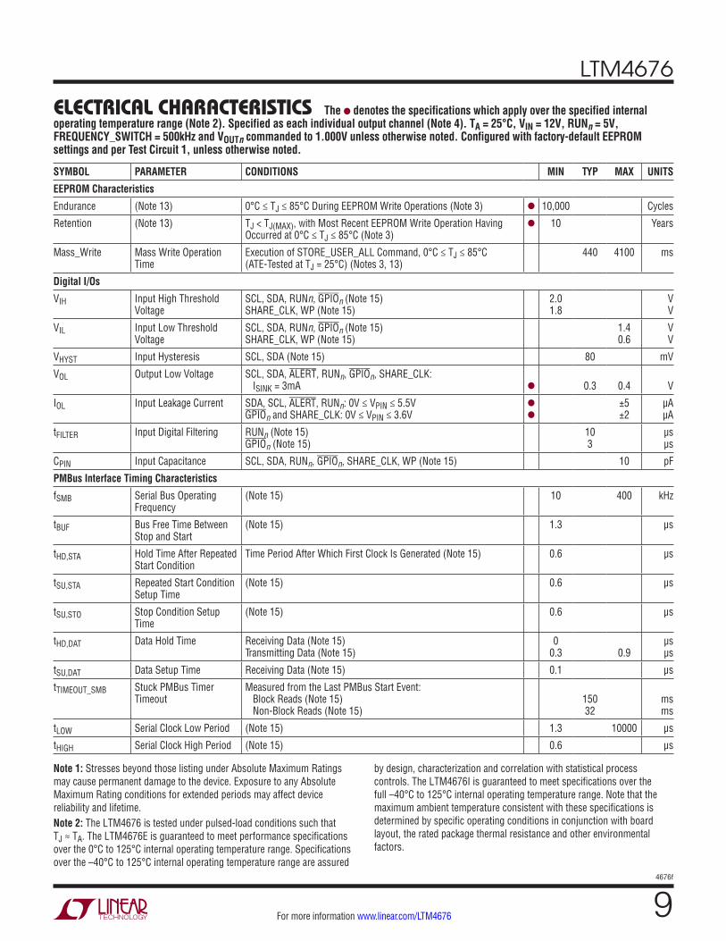
EEPROM Characteristics
Endurance (Note 13) 0°C ≤ TJ ≤ 85°C During EEPROM Write Operations (Note 3) l 10,000 Cycles
Retention (Note 13) TJ < TJ(MAX), with Most Recent EEPROM Write Operation Having Occurred at 0°C ≤ TJ ≤ 85°C (Note 3)
l 10 Years
Mass_Write Mass Write Operation Time
Execution of STORE_USER_ALL Command, 0°C ≤ TJ ≤ 85°C (ATE-Tested at TJ = 25°C) (Notes 3, 13)
440 4100 ms
Digital I/Os
VIH Input High Threshold Voltage
SCL, SDA, RUNn, GPIOn (Note 15) SHARE_CLK, WP (Note 15)
2.0 1.8
V V
VIL Input Low Threshold Voltage
SCL, SDA, RUNn, GPIOn (Note 15) SHARE_CLK, WP (Note 15)
1.4 0.6
V V
VHYST Input Hysteresis SCL, SDA (Note 15) 80 mV
VOL Output Low Voltage SCL, SDA, ALERT, RUNn, GPIOn, SHARE_CLK: ISINK = 3mA
l
0.3
0.4
V
IOL Input Leakage Current SDA, SCL, ALERT, RUNn: 0V ≤ VPIN ≤ 5.5V GPIOn and SHARE_CLK: 0V ≤ VPIN ≤ 3.6V
l
l
±5 ±2
µA µA
tFILTER Input Digital Filtering RUNn (Note 15) GPIOn (Note 15)
10 3
µs µs
CPIN Input Capacitance SCL, SDA, RUNn, GPIOn, SHARE_CLK, WP (Note 15) 10 pF
PMBus Interface Timing Characteristics
fSMB Serial Bus Operating Frequency
(Note 15) 10 400 kHz
tBUF Bus Free Time Between Stop and Start
(Note 15) 1.3 μs
tHD,STA Hold Time After Repeated Start Condition
Time Period After Which First Clock Is Generated (Note 15) 0.6 µs
tSU,STA Repeated Start Condition Setup Time
(Note 15) 0.6 μs
tSU,STO Stop Condition Setup Time
(Note 15) 0.6 μs
tHD,DAT Data Hold Time Receiving Data (Note 15) Transmitting Data (Note 15)
0 0.3
0.9
µs µs
tSU,DAT Data Setup Time Receiving Data (Note 15) 0.1 μs
tTIMEOUT_SMB Stuck PMBus Timer Timeout
Measured from the Last PMBus Start Event: Block Reads (Note 15) Non-Block Reads (Note 15)
150 32
ms ms
tLOW Serial Clock Low Period (Note 15) 1.3 10000 μs
tHIGH Serial Clock High Period (Note 15) 0.6 μs
Note 1: Stresses beyond those listing under Absolute Maximum Ratings may cause permanent damage to the device. Exposure to any Absolute Maximum Rating conditions for extended periods may affect device reliability and lifetime.Note 2: The LTM4676 is tested under pulsed-load conditions such that TJ ≈ TA. The LTM4676E is guaranteed to meet performance specifications over the 0°C to 125°C internal operating temperature range. Specifications over the –40°C to 125°C internal operating temperature range are assured
by design, characterization and correlation with statistical process controls. The LTM4676I is guaranteed to meet specifications over the full –40°C to 125°C internal operating temperature range. Note that the maximum ambient temperature consistent with these specifications is determined by specific operating conditions in conjunction with board layout, the rated package thermal resistance and other environmental factors.

LTM4676
104676f
For more information www.linear.com/LTM4676
ELECTRICAL CHARACTERISTICSNote 3: The LTM4676’s EEPROM temperature range for valid write commands is 0°C to 85°C. To achieve guaranteed EEPROM data retention, execution of the “STORE_USER_ALL” command—i.e., uploading RAM contents to NVM—outside this temperature range is not recommended. However, as long as the LTM4676’s EEPROM temperature is less than 130°C, the LTM4676 will obey the STORE_USER_ALL command. Only when EEPROM temperature exceeds 130°C, the LTM4676 will not act on any STORE_USER_ALL transactions: instead, the LTM4676 NACKs the serial command and asserts its relevant CML (communications, memory, logic) fault bits. EEPROM temperature can be queried prior to commanding STORE_USER_ALL; see the Applications Information section. Note 4: The two power inputs—VIN0 and VIN1—and their respective power outputs—VOUT0 and VOUT1—are tested independently in production. A shorthand notation is used in this document that allows these parameters to be refered to by “VINn” and “VOUTn”, where n is permitted to take on a value of 0 or 1. This italicized, subscripted “n ” notation and convention is extended to encompass all such pin names, as well as register names with channel-specific, i.e., paged data. For example, VOUT_COMMANDn refers to the VOUT_COMMAND command code data located in Pages 0 and 1, which in turn relate to Channels 0 (VOUT0) and Channel 1 (VOUT1). Registers containing non-page-specific data, i.e., whose data is “global” to the module or applies to both of the module's Channels lack the italicized, subscripted “n ”, e.g., FREQUENCY_SWITCH.Note 5: VOUTn (DC) and line and load regulation tests are performed in production with digital servo disengaged (MFR_PWM_MODEn[6] = 0b) and low VOUTn range selected (MFR_PWM_CONFIG[6-n ] = 1b. The digital servo control loop is exercised in production (setting MFR_PWM_MODEn[6] = 1b), but convergence of the output voltage to its final settling value is not necessarily observed in final test—due to potentially long time constants involved—and is instead guaranteed by the output voltage readback accuracy specification. Evaluation in application demonstrates capability; see the Typical Performance Characteristics section.Note 6: See output current derating curves for different VIN, VOUT, and TA, located in the Applications Information section.Note 7: Even though VOUT0 and VOUT1 and their associated current-sensing pins (ISNSn [a/b][+/–]) are specified for 6V absolute maximum and recommended for not more than 5.5V continuous, the maximum recommended command voltage to regulate output channels 0 and 1 is: 4.0V and 5.4V, respectively, when the VOUT range setting for those channels—MFR_PWM_CONFIG’s bits 6 and 5, respectively—are set to “high range”, i.e., 0b; and 2.5V for any channel whose respective MFR_PWM_CONFIG VOUT range-setting bit is set to “low range”, i.e., 1b.
Note 8: Minimum on-time is tested at wafer sort.Note 9: Data conversion is performed in round-robin (cyclic) fashion. All telemetry signals are continuously digitized, and reported data is based on measurements not older than 120ms, typical.Note 10: The following telemetry parameters are formatted in PMBus-defined “Linear Data Format”, in which each register contains a word comprised of 5 most significant bits—representing a signed exponent, to be raised to the power of 2—and 11 least significant bits—representing a signed mantissa: input voltage (on SVIN), accessed via the READ_VIN command code; output currents (IOUTn), accessed via the READ_IOUTn command codes; module input current (IVIN0 + IVIN1 + ISVIN), accessed via the READ_IIN command code; channel input currents (IVINn + 1/2 • ISVIN), accessed via the MFR_READ_IINn command codes;and duty cycles of channel 0 and channel 1 switching power stages, accessed via the READ_DUTY_CYCLEn command codes. This data format limits the resolution of telemetry readback data to 10 bits even though the internal ADC is 16 bits and the LTM4676’s internal calculations use 32-bit words.Note 11: The absolute maximum rating for the SVIN pin is 28V. Input voltage telemetry (READ_VIN) is obtained by digitizing a voltage scaled down from the SVIN pin. Note 12: These typical parameters are based on bench measurements and are not production tested.Note 13: EEPROM endurance and retention are guaranteed by wafer-level testing for data retention. The minimum retention specification applies for devices whose EEPROM has been cycled less than the minimum endurance specification, and whose EEPROM data was written to at 0°C ≤ TJ ≤ 85°C. The RESTORE_USER_ALL command (downloading NVM contents to RAM) is valid over the entire operating temperature range and does not influence EEPROM characteristics. Note 14: V0OU-ACC OV/UV comparator threshold accuracy for MFR_PWM_CONFIG[6] = 1b tested in ATE at VVOSNS0
+ – VVOSNS0– =
0.5V and 2.7V. 1V condition tested at IC-Level, only. V1OU-ACC OV/UV comparator threshold accuracy for MFR_PWM_CONFIG[5] = 1b tested in ATE with VVOSNS1-VSGND = 0.5V and 2.7V. 1.5V condition tested at IC-level, only.Note 15: Tested at IC-level ATE.

LTM4676
114676f
For more information www.linear.com/LTM4676
TYPICAL PERFORMANCE CHARACTERISTICS
Efficiency vs Output Current, 5VIN, VOUT0 and VOUT1 Paralleled, VIN = SVIN = VINn = INTVCC, MFR_PWR_MODEn[1:0] = 10b
Efficiency vs Output Current, VOUT1 = 5V, VOUT0 = OFF, VIN = SVIN = VINn, INTVCC Open, MFR_PWR_MODEn[1:0] = 10b
Efficiency vs Output Current, 24VIN, VOUT0 and VOUT1 Paralleled, VIN = SVIN = VINn, INTVCC Open, MFR_PWR_MODEn[1:0] = 10b
Efficiency vs Output Current, 8VIN, VOUT0 and VOUT1 Paralleled, VIN = SVIN = VINn, INTVCC Open,MFR_PWR_MODEn[1:0] = 10b
Single Phase Single Output Burst Mode Efficiency, VIN = SVIN = VINn, INTVCC Open, MFR_PWR_MODEn[1:0] = 01b
Efficiency vs Output Current, 12VIN, VOUT0 and VOUT1 Paralleled, VIN = SVIN = VINn, INTVCC Open,MFR_PWR_MODEn[1:0] = 10b
TA = 25°C, 12VIN to 1VOUT, unless otherwise noted.
OUTPUT CURRENT (A)0 2 4
80
90
22 24 26
4676 G01
70
606 8 10 12 14 16 18 20
100
75
85
65
95
3.3VOUT, 425kHz2.5VOUT, 425kHz1.8VOUT, 425kHz1.5VOUT, 350kHz1.2VOUT, 350kHz1.0VOUT, 350kHz0.9VOUT, 350kHz
EFFI
CIEN
CY (%
)
OUTPUT CURRENT (A)0 2 4
80
90
22 24 26
4676 G02
70
606 8 10 12 14 16 18 20
100
75
85
65
95
3.3VOUT, 575kHz2.5VOUT, 500kHz1.8VOUT, 425kHz1.5VOUT, 350kHz1.2VOUT, 350kHz1.0VOUT, 350kHz0.9VOUT, 350kHz
EFFI
CIEN
CY (%
)
OUTPUT CURRENT (A)0 2 4
80
90
22 24 26
4676 G03
70
606 8 10 12 14 16 18 20
100
75
85
65
95
3.3VOUT, 650kHz2.5VOUT, 575kHz1.8VOUT, 500kHz1.5VOUT, 425kHz1.2VOUT, 350kHz1.0VOUT, 350kHz0.9VOUT, 350kHz
EFFI
CIEN
CY (%
)
OUTPUT CURRENT (A)0 2 4
80
90
22 24 26
4676 G04
70
606 8 10 12 14 16 18 20
100
75
85
65
953.3VOUT, 750kHz2.5VOUT, 650kHz1.8VOUT, 500kHz1.5VOUT, 425kHz
1.2VOUT, 350kHz1.0VOUT, 250kHz0.9VOUT, 250kHz
EFFI
CIEN
CY (%
)
OUTPUT CURRENT (A)0 1 2
80
90
11 12 13
4676 G05
70
603 4 5 6 7 8 9 10
100
75
85
65
95
8VIN, 500kHz12VIN, 750kHz24VOUT, 1MHz
EFFI
CIEN
CY (%
)
OUTPUT CURRENT (A)0 1 2
50
70
11 12 13
4676 G06
403 4 5 6 7 8 9 10
90
60
80
24VIN TO 5VOUT, 1MHz12VIN TO 1.5VOUT, 425kHz
EFFI
CIEN
CY (%
)

LTM4676
124676f
For more information www.linear.com/LTM4676
TYPICAL PERFORMANCE CHARACTERISTICS TA = 25°C, 12VIN to 1VOUT, unless otherwise noted.
Dual Phase Single Output Load Transient Response,12VIN to 1VOUT
Single Phase Single Output Load Transient Response,12VIN to 1VOUT
Dual Phase Single Output Load Transient Response, 5VIN to 1VOUT
Dual Output Concurrent Rail Start-Up/Shutdown
Dual Output Start-Up/Shutdown with a Pre-Biased Load
Single Phase Single Output Short-Circuit Protection at No Load
Single Phase Single Output Load Transient Response, 24VIN to 1VOUT
Single Phase Single Output Load Transient Response, 24VIN to 3.3VOUT
Single Phase Single OutputPulse-Skipping (Discontinuous) Mode Efficiency,VIN = SVIN = VINn, INTVCC Open, MFR_PWR_MODEn[1:0] = 00b
OUTPUT CURRENT (A)0 1 2
50
70
11 12 13
4676 G07
403 4 5 6 7 8 9 10
90
60
80
24VIN TO 5VOUT, 1MHz12VIN TO 1.5VOUT, 425kHz
EFFI
CIEN
CY (%
)
VOUT50mV/DIV
AC-COUPLED
IOUT8A/DIV
40µs/DIVFIGURE 34 CIRCUIT AT 12VIN, INTVCC PINOPEN CIRCUIT AND VOUT_COMMANDn SETTO 1.000V. 0A TO 20A LOAD STEP AT 20A/µs
4676 G08
VOUT050mV/DIV
AC-COUPLED
IOUT4A/DIV
40µs/DIVFIGURE 41 CIRCUIT AT 12VIN0A TO 10A LOAD STEP AT 10A/µs
4676 G09
VOUT50mV/DIV
AC-COUPLED
IOUT8A/DIV
40µs/DIVFIGURE 34 CIRCUIT AT 5VIN, VOUT_COMMANDn SET TO 1.000V. 0A TO 20A LOAD STEP AT 20A/µs
4676 G10
VOUT050mV/DIV
AC-COUPLED
IOUT4A/DIV
40µs/DIVFIGURE 41 CIRCUIT AT 24VIN0A TO 10A LOAD STEP AT 10A/µs
4676 G11
VOUT050mV/DIV
AC-COUPLED
IOUT4A/DIV
40µs/DIVFIGURE 41 CIRCUIT AT 24VIN, COUT0 = 5× 100µFAND VOUT0 COMMANDED TO 3.300V. 0A TO 10A LOAD STEP AT 10A/µs
4676 G12
VOUT0, VOUT1500mV/DIV
IOUT05A/DIV
RUN0, RUN15A/DIV
2ms/DIVFIGURE 41 CIRCUIT AT 12VIN, 77mΩ LOAD ONVOUT0, NO LOAD ON VOUT1. TON_RISE0 = 3ms,TON_RISE1 = 5.297ms, TOFF_DELAY1 = 0ms,TOFF_DELAY0 = 2.43ms, TOFF_FALL1 = 5.328ms,TOFF_FALL0 = 3ms, ON_OFF_CONFIG = 0x1E
4676 G13
VOUT0, VOUT1500mV/DIV
IDIODE1mA/DIV
RUN0, RUN15A/DIV
2ms/DIVFIGURE 41 CIRCUIT AT 12VIN, 77mΩ LOAD ONVOUT0, 500Ω ON VOUT1. VOUT1 PRE-BIASEDTHROUGH A DIODE. TON_RISE0 = 3ms,TON_RISE1 = 5.297ms, TOFF_DELAY1 = 0ms,TOFF_DELAY0 = 2.43ms, TOFF_FALL1 = 5.328ms,TOFF_FALL0 = 3ms, ON_OFF_CONFIG = 0x1F
4676 G14
VOUT0200mV/DIV
IIN01A/DIV
10µs/DIVFIGURE 41 CIRCUIT AT 12VIN, NO LOAD ON VOUT0 PRIOR TO APPLICATION OF SHORT CIRCUIT
4676 G15

LTM4676
134676f
For more information www.linear.com/LTM4676
READ_TEMPERATURE_2 (Control IC Temperature Error) vs Junction Temperature, RUNn = 0V
READ_VIN (Input VoltageReadback Telemetry) Error vs SVIN, RUNn = 0V
MFR_READ_IINn (Input Current Readback) Error vs (IVINn + ISVIN), FCM, IOUTnSwept from 0A to 13A, One Channel at a Time, RUN1-n = 0V
Single Phase Single Output Short-Circuit Protection at Full Load
READ_VOUTn (Output Voltage Readback) Error vs VOUTn IOUTn = No Load, RUN1-n = 0V
READ_IOUTn (Output Current Readback) Error vs IOUTn
TYPICAL PERFORMANCE CHARACTERISTICS TA = 25°C, 12VIN to 1VOUT, unless otherwise noted.
ACTUAL TEMPERATURE (°C)–45
–1.0
MEA
SURE
MEN
T ER
ROR
(°C)
–0.8
–0.4
–0.2
0
1.0
0.4
–5 35 55
4676 G19
–0.6
0.6
0.8
0.2
–25 15 75 95 115
VOUT0200mV/DIV
IIN01A/DIV
10µs/DIVFIGURE 41 CIRCUIT AT 12VIN, 77mΩ LOAD ON VOUT0 PRIOR TO APPLICATION OF SHORT CIRCUIT
4676 G16
VOUT (V)0.5
MEA
SURE
MEN
T ER
ROR
(mV)
0
20
40
60
4.5
4676 G17
–20
–40
–10
10
30
50
–30
–50
–601.5 2.5 3.51.0 5.02.0 3.0 4.0 5.5
SPECIFIED UPPER LIMIT
SPECIFIED LOWER LIMIT
CHANNEL 0
CHANNEL 1
IOUT (A)0
–300
MEA
SURE
MEN
T ER
ROR
(mA)
–200
–100
0
100
CHANNEL 0
CHANNEL 1
200
300
3.25 6.50 9.75 13.00
SPECIFIED UPPER LIMIT
SPECIFIED LOWER LIMIT
4676 G18
SVIN (V)4
–600
MEA
SURE
MEN
T ER
ROR
(mV)
–400
–200
0
200
400
600
10 16 22 28
SPECIFIED UPPER LIMIT
SPECIFIED LOWER LIMIT
4676 G20
IINn + ISVIN (A)0
–200
MEA
SURE
MEN
T ER
ROR
(mA)
–100
0
100
200
0.2 0.4 0.6 0.8
4676 G21
1.0 1.2 1.4
CHANNEL 0
CHANNEL 1
SPECIFIED UPPER LIMIT
SPECIFIED LOWER LIMIT

LTM4676
144676f
For more information www.linear.com/LTM4676
PIN FUNCTIONSPACKAGE ROW AND COLUMN LABELING MAY VARY AMONG µModule PRODUCTS. REVIEW EACH PACKAGE LAYOUT CAREFULLY.
GND (A4, A6-10, B4-B9, C4, C6-C9, D4, D7, E3, F3, F10, G3, G10-12, H3, H10, J4, J10, K4, K7-9, L4-9, M4, M6-10): Power Ground of the LTM4676. Power return for VOUT0 and VOUT1.
VOUT0 (A1-3, B1-3, C1-3, D1-3): Channel 0 Output Voltage.
VOSNS0+ (D9): Channel 0 Positive Differential Voltage Sense
Input. Together, VOSNS0+ and VOSNS0
– serve to kelvin-sense the VOUT0 output voltage at VOUT0’s point of load (POL) and provide the differential feedback signal directly to Channel 0’s feedback loop. VOUT0 can regulate up to 4.0V output. Command VOUT0’s target regulation voltage by serial bus. Its initial command value at SVIN power-up is dictated by NVM (non-volatile memory) contents (factory default: 1.000V)—or, optionally, may be set by configuration resistors; see VOUT0CFG, VTRIM0CFG and the Applications Information section.
VOSNS0– (E9): Channel 0 Negative Differential Voltage
Sense Input. See VOSNS0+.
TYPICAL PERFORMANCE CHARACTERISTICS TA = 25°C, 12VIN to 1VOUT, unless otherwise noted.
READ_OUT of 20 LTM4676s (DC1811) 12VIN, 1VOUT, TJ = –40°C, IOUTn = 13A, System Having Reached Thermally Steady-State Condition, No Airflow
READ_OUT of 20 LTM4676s (DC1811) 12VIN, 1VOUT, TJ = 25°C, IOUTn = 13A, System Having Reached Thermally Steady-State Condition, No Airflow
READ_OUT of 20 LTM4676s (DC1811) 12VIN, 1VOUT, TJ = 125°C, IOUTn = 13A, System Having Reached Thermally Steady-State Condition, No Airflow
READ_IOUT CHANNEL READBACK (A)
13.1
2500
13.1
5625
13.1
8750
13.2
1875
13.2
5000
13.2
8125
13.3
1250
13.3
4375
13.3
7500
0
NUM
BER
OF C
HANN
ELS
2
4
6
8
10
12
4676 G22 READ_IOUT CHANNEL READBACK (A)
13.0
0000
13.0
3125
13.0
6250
13.0
9375
13.1
2500
13.1
5625
13.1
8750
13.2
1875
13.2
5000
0
NUM
BER
OF C
HANN
ELS
2
4
6
8
10
12
4676 G23 READ_IOUT CHANNEL READBACK (A)
12.9
6875
13.0
0000
13.0
3125
13.0
6250
13.0
9375
13.1
2500
13.1
8750
13.1
5625
13.2
1875
0
NUM
BER
OF C
HANN
ELS
2
4
6
8
10
12
4676 G24
VORB0+ (D10): Channel 0 Positive Readback Pin. Shorted
to VOSNS0+ internal to the LTM4676. If desired, place a test
point on this node and measure its impedance to VOUT0 on one’s hardware (e.g., motherboard, during in circuit test (ICT) post-assembly process) to provide a means of verifying the integrity of the feedback signal connection between VOSNS0
+ and VOUT0.
VORB0– (E10): Channel 0 Negative Readback Pin. Shorted
to VOSNS0– internal to the LTM4676. If desired, place a
test point on this node and measure its impedance to GND on one’s hardware (e.g., motherboard, during ICT post-assembly process) to provide a means of verifying the integrity of the feedback signal connection between VOSNS0
– and GND (VOUT0 power return).
VOUT1 (J1-3, K1-3, L1-3, M1-3): Channel 1 Output Voltage.
VOSNS1 (H9): Channel 1 Positive Voltage Sense Input. To-gether, VOSNS1 and SGND serve to kelvin-sense the VOUT1 output voltage at VOUT1’s POL and provide the differential feedback signal directly to Channel 1’s feedback loop. VOUT1 can regulate up to 5.4V output. Command VOUT1’s target regulation voltage by serial bus. Its initial command value at SVIN power-up is dictated by NVM (non-volatile

LTM4676
154676f
For more information www.linear.com/LTM4676
PIN FUNCTIONSmemory) contents (factory default: 1.000V)—or, option-ally, may be set by configuration resistors; see VOUT1CFG, VTRIM1CFG and the Applications Information section.
SGND (F7-8, G7-8): Channel 1 Negative Differential Volt-age Sense Input. See VOSNS1. Additionally, SGND is the signal ground return path of the LTM4676. If desired, one may place a test point on one of the four SGND pins and measure its impedance to GND on one’s hardware (e.g., motherboard, during ICT post-assembly process) to pro-vide a means of verifying the integrity of the feedback signal connection between the other three SGND pins and GND (VOUT1 power return). SGND is not electrically connected to GND internal to the LTM4676. Connect SGND to GND at VOUT1’s POL negative voltage sense point.
VORB1 (J9): Channel 1 Positive Readback Pin. Shorted to VOSNS1 internal to the LTM4676. At one’s option, place a test point on this node and measure its impedance to VOUT1 on one’s hardware (e.g., motherboard, during ICT post-assembly process) to provide a means of verifying the integrity of the feedback signal connection between VOUT1 and VOSNS1.
VIN0 (A11-12, B11-12, C11-12, D11-12, E12): Positive Power Input to Channel 0 Switching Stage. Provide suf-ficient decoupling capacitance in the form of multilayer ceramic capacitors (MLCCs) and low ESR electrolytic (or equivalent) to handle reflected input current ripple from the step-down switching stage. MLCCs should be placed as close to the LTM4676 as physically possible. See Layout Recommendations in the Applications Information section.
VIN1 (H12, J11-12, K11-12, L11-12, M11-12): Positive Power Input to Channel 1 Switching Stage. Provide suf-ficient decoupling capacitance in the form of MLCCs and low ESR electrolytic (or equivalent) to handle reflected input current ripple from the step-down switching stage. MLCCs should be placed as close to the LTM4676 as physically possible. See Layout Recommendations in the Applications Information section.
SW0 (B10): Switching Node of Channel 0 Step-Down Converter Stage. Used for test purposes or EMI-snubbing heavier than that supported by SNUB0. May be routed a short distance to a local test point to monitor switching
action of Channel 0, if desired, but do not route near any sensitive signals; otherwise, leave electrically isolated (open).
SW1 (L10): Switching Node of Channel 1 Step-Down Converter Stage. Used for test purposes or EMI-snubbing heavier than that supported by SNUB1. May be routed a short distance to a local test point to monitor switching action of Channel 1, if desired, but do not route near any sensitive signals; otherwise, leave open.
SNUB0 (A5): Access to Channel 0 Switching Stage Snubber Capacitor. Connecting an optional resistor from SNUB0 to GND can reduce radiated EMI, with only a minor penalty towards power conversion efficiency. See the Applications Information section. Pin should otherwise be left open.
SNUB1 (M5): Access to Channel 1 Switching Stage Snubber Capacitor. Connecting an optional resistor from SNUB0 to GND can reduce radiated EMI, with only a minor penalty towards power conversion efficiency. See the Applications Information section. Pin should otherwise be left open.
SVIN (F11-12): Input Supply for LTM4676’s Internal Control IC. In most applications, SVIN connects to VIN0 and/or VIN1, in which case no external decoupling beyond that already allocated for VIN0/VIN1 is required. If SVIN is operated from an auxiliary supply separate from VIN0/VIN1, decouple this pin to GND with a capacitor (0.1μF to 1μF).
INTVCC (F9, G9): Internal Regulator, 5V Output. When operating the LTM4676 from 5.75V ≤ SVIN ≤ 26.5V, an LDO generates INTVCC from SVIN to bias internal control circuits and the MOSFET drivers of the LTM4676. No exter-nal decoupling is required. INTVCC is regulated regardless of the RUNn pin state. When operating the LTM4676 with 4.5V ≤ SVIN < 5.75V, INTVCC must be electrically shorted to SVIN.
VDD33 (J7): Internally Generated 3.3V Power Supply Output Pin. This pin should only be used to provide ex-ternal current for the pull-up resistors required for GPIOn, SHARE_CLK, and SYNC, and may be used to provide external current for pull-up resistors on RUNn, SDA, SCL and ALERT. No external decoupling is required.

LTM4676
164676f
For more information www.linear.com/LTM4676
PIN FUNCTIONSVDD25 (J6): Internally Generated 2.5V Power Supply Output Pin. Do not load this pin with external current; it is used strictly to bias internal logic and provides current for the internal pull-up resistors connected to the configuration-programming pins. No external decoupling is required.
ASEL (G4): Serial Bus Address Configuration Pin. On any given I2C/SMBus serial bus segment, every device must have its own unique slave address. If this pin is left open, the LTM4676 powers up to its default slave address of 0x4F (hexadecimal), i.e., 1001111b (industry standard convention is used throughout this document: 7-bit slave addressing). The lower four bits of the LTM4676’s slave address can be altered from this default value by connecting a resistor from this pin to SGND—hence configuring the 7-bit slave address of the LTM4676 to one of 16 supported values. Minimize capacitance—especially when the pin is left open—to assure accurate detection of the pin state.
FSWPHCFG (H4): Switching Frequency, Channel Phase-Interleaving Angle and Phase Relationship to SYNC Configuration Pin. If this pin is left open—or, if the LTM4676 is configured to ignore pin-strap (RCONFIG) resistors, i.e., MFR_CONFIG_ALL[6] = 1b—then the LTM4676’s switching frequency (FREQUENCY_SWITCH) and channel phase relationships (with respect to the SYNC clock; MFR_PWM_CONFIG[2:0]) are dictated at SVIN power-up according to the LTM4676’s NVM contents. Default factory values are: 500kHz operation; Channel 0 at 0°; and Channel 1 at 180°C (convention throughout this document: a phase angle of 0° means the channel’s switch node rises coincident with the falling edge of the SYNC pulse). Connecting a resistor from this pin to SGND (and using the factory-default NVM setting of MFR_CONFIG_ALL[6] = 0b) allows a convenient way to configure multiple LTM4676s with identical NVM contents for different switching frequen-cies of operation and phase interleaving angle settings of intra- and extra-module-paralleled channels—all, without GUI intervention or the need to “custom pre-program” module NVM contents. (See the Applications Information section.) Minimize capacitance—especially when the pin is left open—to assure accurate detection of the pin state.
VOUT0CFG (G5): Output Voltage Select Pin for VOUT0, Coarse Setting. If the VOUT0CFG and VTRIM0CFG pins are both left open—or, if the LTM4676 is configured to ignore
pin-strap (RCONFIG) resistors, i.e., MFR_CONFIG_ALL[6] = 1b—then the LTM4676’s target VOUT0 output voltage setting (VOUT_COMMAND0) and associated power-good and OV/UV warning and fault thresholds are dictated at SVIN power-up according to the LTM4676’s NVM contents. A resistor connected from this pin to SGND—in combination with resistor pin settings on VTRIM0CFG, and using the factory-default NVM setting of MFR_CONFIG_ALL[6] = 0b—can be used to config-ure the LTM4676’s Channel 0 output to power-up to a VOUT_COMMAND value (and associated output voltage monitoring and protection/fault-detection thresholds) different from those of NVM contents. (See the Applications Information section.) Connecting resistor(s) from VOUT0CFG to SGND and/or VTRIM0CFG to SGND in this manner allows a convenient way to configure multiple LTM4676s with identical NVM contents for different output voltage settings—all without GUI intervention or the need to “custom-pre-program” module NVM contents. Minimize capacitance—especially when the pin is left open—to assure accurate detection of the pin state. Note that use of RCONFIGs on VOUT0CFG/VTRIM0CFG can affect the VOUT0 range setting (MFR_PWM_CONFIG[6]) and loop gain.
VTRIM0CFG (H5): Output Voltage Select Pin for VOUT0, Fine Setting. Works in combination with VOUT0CFG to affect the VOUT_COMMAND (and associated output voltage monitoring and protection/fault-detection thresholds) of Channel 0, at SVIN power-up. (See VOUT0CFG and the Applications Information section.) Minimize capacitance—especially when the pin is left open—to assure accurate detection of the pin state. Note that use of RCONFIGs on VOUT0CFG/VTRIM0CFG can affect the VOUT0 range setting (MFR_PWM_CONFIG[6]) and loop gain.
VOUT1CFG (G6): Output Voltage Select Pin for VOUT1, Coarse Setting. If the VOUT1CFG and VTRIM1CFG pins are both left open—or, if the LTM4676 is configured to ignore pin-strap (RCONFIG) resistors, i.e., MFR_CONFIG_ALL[6] = 1b—then the LTM4676’s target VOUT1 output voltage setting (VOUT_COMMAND1) and associated power good and OV/UV warning and fault thresholds are dictated at SVIN power-up according to the LTM4676’s NVM contents, in precisely the same fashion that the VOUT0CFG and VTRIM0CFG pins affect the respective settings of VOUT0/Channel 0. (See VOUT0CFG, VTRIM0CFG and the Applications Information
LTM4676
174676f
For more information www.linear.com/LTM4676
PIN FUNCTIONSsection.) Minimize capacitance—especially when the pin is left open—to assure accurate detection of the pin state. Note that use of RCONFIGs on VOUT1CFG/VTRIM1CFG can affect the VOUT1 range setting (MFR_PWM_CONFIG[5]) and loop gain.
VTRIM1CFG (H6): Output Voltage Select Pin for VOUT1, Fine Setting. Works in combination with VOUT1CFG to affect the VOUT_COMMAND (and associated output voltage monitoring and protection/fault-detection thresholds) of Channel 1, at SVIN power-up. (See VOUT1CFG and the Applications Information section.) Minimize capacitance—especially when the pin is left open—to assure accurate detection of the pin state. Note that use of RCONFIGs on VOUT1CFG/VTRIM1CFG can affect the VOUT1 range setting (MFR_PWM_CONFIG[5]) and loop gain.
SYNC (E7): PWM Clock Synchronization Input and Open-Drain Output Pin. The setting of the FREQUENCY_SWITCH register dictates whether the LTM4676 is a “sync master” or “sync slave” module. When the LTM4676 is a sync master, FREQUENCY_SWITCH contains the commanded switching frequency of Channels 0 and 1—in PMBus linear data format—and it drives its SYNC pin low for 500ns at a time, at this commanded rate. Whereas, a sync slave uses FREQUENCY_SWITCH=0x0000 and does not pull its SYNC pin low. The LTM4676’s PLL synchronizes the LTM4676’s PWM clock to the waveform present on the SYNC pin—and therefore, a resistor pull-up to 3.3V is required in the application, regardless of whether the LTM4676 is a sync master or slave. EXCEPTION: driving the SYNC pin with an external clock is permissible; see the Applications Information section for details.
SCL (E6): Serial Bus Clock Open-Drain Input (Can Be an Input and Output, if Clock Stretching is Enabled). A pull-up resistor to 3.3V is required in the application for digital communication to the SMBus master(s) that nominally drive this clock. The LTM4676 will never encounter scenarios where it would need to engage clock stretching unless SCL communication speeds exceed 100kHz—and even then, LTM4676 will not clock stretch unless clock stretching is enabled by means of setting MFR_CONFIG_ALL[1] = 1b. The factory-default NVM configuration setting has MFR_CONFIG_ALL[1] = 0b: clock stretching disabled. If communication on the bus at
clock speeds above 100kHz is required, the user’s SMBus master(s) need to implement clock stretching support to assure solid serial bus communications, and only then should MFR_CONFIG_ALL[1] be set to 1b. When clock stretching is enabled, SCL becomes a bidirectional, open-drain output pin on LTM4676.
SDA (D6): Serial Bus Data Open-Drain Input and Output. A pull-up resistor to 3.3V is required in the application.
ALERT (E5): Open-Drain Digital Output. A pull-up resistor to 3.3V is required in the application only if SMBALERT interrupt detection is implemented in one’s SMBus system.
SHARE_CLK (H7): Share Clock, Bidirectional Open-Drain Clock Sharing Pin. Nominally 100kHz. Used for synchronizing the time base between multiple LTM4676s (and any other Linear Technology devices with a SHARE_CLK pin)—to realize well-defined rail sequencing and rail tracking. Tie the SHARE_CLK pins of all such devices together; all devices with a SHARE_CLK pin will synchronize to the fastest clock. A pull-up resistor to 3.3V is only re-quired when synchronizing the time base between devices.
GPIO0, GPIO1 (E4 and F4, Respectively): Digital, Programmable General Purpose Inputs and Outputs. Open-drain outputs and/or high impedance inputs. The LTM4676’s factory-default NVM configurations for MFR_GPIO_PROPAGATEn—0x6893—and MFR_GPIO_RESPONSEn—0xC0—are such that: (1) when a channel-specific fault condition is detected—such as channel OT (overtemperature) or output UV/OV—the respective GPIOn pin pulls logic low; (2) when a non-channel specific fault condition is detected—such as input OV or control IC OT—both GPIOn pins pull logic low; (3) the LTM4676 ceases switching action on Channel 0 and 1 when its respective GPIOn pin is logic low. Most significantly, this default configuration provides for graceful integration and interoperation of LTM4676 with paralleled channel(s) of other LTM4676(s)—in terms of properly coordinating efforts in starting, ceasing, and resuming switching action and output voltage regulation, in unison—all without GUI intervention or the need to “custom-preprogram” module NVM contents. Pull-up resistors from GPIOn to 3.3V are required for proper operation in the vast majority of applications. (Only if the LTM4676’s MFR_GPIO_RESPONSEn value were set to 0x00 might pull-ups be

LTM4676
184676f
For more information www.linear.com/LTM4676
PIN FUNCTIONSunnecessary. See the Applications Information section for details.)
WP (K6): Write Protect Pin, Active High. An internal 10μA current source pulls this pin to VDD33. If WP is open circuit or logic high, only I2C writes to PAGE, OPERATION, CLEAR_FAULTS, MFR_CLEAR_PEAKS and MFR_EE_UNLOCK are supported. Additionally, Individual faults can be cleared by writing 1b’s to bits of interest in registers prefixed with “STATUS”. If WP is low, I2C writes are unrestricted.
RUN0, RUN1 (F5 and F6, Respectively): Enable Run Input for Channels 0 and 1, Respectively. Open-drain input and output. Logic high on these pins enables the respective outputs of the LTM4676. These open-drain output pins hold the pin low until the LTM4676 is out of reset and SVIN is detected to exceed VIN_ON. A pull-up resistor to 3.3V is required in the application. The LTM4676 pulls RUN0 and/or RUN1 low, as appropriate, when a global fault and/or channel-specific fault occurs whose fault response is configured to latch off and cease regulation; issuing a CLEAR_FAULTS command via I2C or power-cycling SVIN is necessary to restart the module, in such cases. Do not pull RUN logic high with a low impedance source.
TSNS0a, TSNS1a (D5 and J5, Respectively): Temperature Sensor Excitation and Measurement Ports for Channels 0 and 1, Respectively. Normally, connect these pins to TSNS0b and TSNS1b, respectively, to allow the LTM4676 to monitor its Channel 0 and 1 internal thermal sensors. See the Applications Information section for information on how to use TSNS1a to monitor an auxiliary (outside) temperature sensor, e.g., a PN junction on the die of a microprocessor.
TSNS0b, TSNS1b (C5 and K5, Respectively): Thermal Sensor Inputs for Channels 0 and 1, Respectively. See TSNS0a and TSNS1a.
ISNS0a+, ISNS1a
+ (F2 and H2, Respectively): Control IC Current Sense Positive Port Inputs—for Channels 0 and 1, respectively. Connect to ISNS0b
+ and ISNS1b+, respectively.
ISNS0b+, ISNS1b
+ (F1 and H1, Respectively): Positive Current Sense Signal Kelvin Connections for Channels 0 and 1, Respectively. See ISNS0a
+ and ISNS1a+.
ISNS0a–, ISNS1a
– (E2 and G2, Respectively): Control IC Current Sense Negative Port Inputs for Channels 0 and 1, Respectively. Connect to ISNS0b
– and ISNS1b–, respectively.
ISNS0b–, ISNS1b
– (E1 and G1, Respectively): Negative Current Sense Signal Kelvin Connections for Channels 0 and 1, Respectively. See ISNS0a
–/ISNS1a–.
COMP0a, COMP1a (E8 and H8, Respectively): Current Control Threshold and Error Amplifier Compensation Nodes for Channels 0 and 1, Respectively. The trip threshold of each channel’s current comparator increases with a respective rise in COMPna voltage. Small filter capacitors (22pF) internal to the LTM4676 on these COMP pins (ter-minated to SGND) introduce high frequency roll off of the error-amplifier response, yielding good noise rejection in the control loop. See COMP0b/COMP1b.
COMP0b, COMP1b (D8 and J8, Respectively): Internal Loop Compensation Networks for Channels 0 and 1, Respectively. For the vast majority of applications, the internal, default loop compensation of the LTM4676 is suitable to apply “as is”, and yields very satisfactory re-sults: apply the default loop compensation to the control loops of Channels 0 and 1 by simply connecting COMP0a to COMP0b and COMP1a to COMP1b, respectively. Whereas, when more specialized applications require a personal touch the optimization of control loop response, this can be easily accomplished by connecting (an) R-C network(s) from COMP0a and/or COMP1a—terminated to SGND—and leaving COMP0b and/or COMP1b open, as desired.
DNC (C10, E11, H11, K10): Do not connect these pins to external circuitry. Solder these pins only to mounting pads on the PC board for mechanical integrity. These pads must remain electrically open circuit.

LTM4676
194676f
For more information www.linear.com/LTM4676
SIMPLIFIED BLOCK DIAGRAM
DECOUPLING REQUIREMENTS
+
+
VIN0
VOUT0
VIN5.75V TO 26.5V
SW0
SNUB0
GND
ISNS0b–
ISNS0b+
ISNS0a+
ISNS0a–
TSNS0b
TSNS0a
VOSNS0+
VOSNS0–
LOCALHIGHFREQMLCCs
x1
COMP0a
COMP0b
VOUT1
SW1
SNUB1
GND
ISNS1b–
ISNS1b+
ISNS1a+
ISNS1a–
TSNS1b
TSNS1a
VOSNS1[+]
SGND [/VOSNS1–]
COMP1aCONTROLLER SIGNAL GND
COMP1b
SYNC
ASEL
4676 F01
VDD25
VOUT0CFG
VTRIM0CFG
VTRIM1CFG
VOUT1CFG
FSWPHCFG
SCL
5V TOLERANT; PULL-UPRESISTORS NOT SHOWN
5V TOLERANT; PULL-UPRESISTORS NOT SHOWN
3.3V TOLERANT; PULL-UPRESISTOR NOT NEEDED
SDA
ALERT
WP
RUN0
RUN1
GPIO0
GPIO1
SHARE_CLK
COUT0LF COUT1LFCOUT1HFCOUT0HF
VOUT0ADJUSTABLEUP TO 4.0VUP TO 13A
SVIN
1µF2.2nF 1µF
MT0
600nH 600nH
THERMALSENSOR
THERMALSENSORMB0
MT1
MB12.2µF 2.2µF
INTVCC VDD33 VIN1
CINHCINL
THERMALSENSOR
ANALOGREADBACKSIGNALS
TO ERRORAMPLIFIER
POWER CONTROLANALOG SECTION
POWER MANAGEMENTDIGITAL SECTION
+–
LOAD0
LOCALHIGHFREQ
MLCCs
LOAD1
+
VOUT1ADJUSTABLEUP TO 5.4VUP TO 13A
2.2nF
INTERNALCOMP
SPISLAVE
SPIMASTER
SYNCDRIVER
OSC(32MHz)
DIGITAL ENGINE
EEPROM
ROM
RAM
INTERNALCOMPADC
3.3V TOLERANT; PULL-UPRESISTORS NOT SHOWN
3.3V TOLERANT; PULL-UPRESISTOR NOT SHOWN
CONFIGURATIONRESISTORS TERMINATINGTO SGND NOT SHOWN
Figure 1. Simplified LTM4676 Block Diagram
SYMBOL PARAMETER CONDITIONS MIN TYP MAX UNITS
CINH External High Frequency Input Capacitor Requirement (5.75V ≤ VIN ≤ 26.5V, VOUTn Commanded to 1.000V)
IOUT0 = 13A, 3 × 22μF, or 4 × 10μF IOUT1 = 13A, 3 × 22μF, or 4 × 10μF
40 66 µF
COUTnHF External High Frequency Output Capacitor Requirement (5.75V ≤ VIN ≤ 26.5V, VOUTn Commanded to 1.000V)
IOUT0 = 13A IOUT1 = 13A
400 400
µF µF
TA = 25°C. Using Figure 1 configuration.

LTM4676
204676f
For more information www.linear.com/LTM4676
FUNCTIONAL DIAGRAM
+
V IN0
C INH
C INL
+C O
UT0L
F
(Com
pute
d To
tal I
nput
Cur
rent
, IVI
NO +
I VIN
1 +
I SVI
N: R
EAD_
IIN)
(Com
pute
d Ch
anne
l 0 In
put C
urre
nt, I
VIN0
+ 1
/2 •
I SVI
N: M
FR_R
EAD_
IIN0)
(Com
pute
d Ch
anne
l 1 In
put C
urre
nt, I
VIN1
+ 1
/2 •
I SVI
N: M
FR_R
EAD_
IIN1)
V IN
5.75
V TO
26.
5V
(SV I
N Te
lem
etry
: RE
AD_V
IN a
nd M
FR_V
IN_P
EAK)
(PW
M0
Tele
met
ry:
READ
_DUT
Y_CY
CLE 0
)(P
WM
1 Te
lem
etry
: RE
AD_D
UTY_
CYCL
E 1)
(I OUT
0 Te
lem
etry
: REA
D_IO
UT0
and
MFR
_IOU
T_PE
AK0)
(I OUT
1 Te
lem
etry
: REA
D_IO
UT1
and
MFR
_IOU
T_PE
AK1)
Chan
nel 0
The
rmal
Sen
sor
(Tel
emet
ry: R
EAD_
TEM
PERA
TURE
_10
and
MFR
_TEM
PERA
TURE
_1_P
EAK 0
)
Chan
nel 1
The
rmal
Sen
sor
(Tel
emet
ry: R
EAD_
TEM
PERA
TURE
_11
and
MFR
_TEM
PERA
TURE
_1_P
EAK 1
)
+
++
––
–
SVIN
INTV
CCV D
D33
V IN1
INT
FILT
ER
MT0
MT1
MB1
MB0
POW
ER C
ONTR
OLAN
ALOG
SEC
TION
V OUT
0
GND
I SNS
0b–
C OUT
0HF
C OUT
1LF
C OUT
1HF
V OUT
0AD
JUST
ABLE
UP T
O 4.
0VUP
TO
13A
V OUT
1AD
JUST
ABLE
UP T
O 5.
4VUP
TO
13A
SW0
SNUB
0
Optio
nal S
nubb
erRe
sist
or fo
r Mod
erat
eRe
duct
ion
in E
MI
(Size
: EIA
0603
~EI
A251
2)
R SNU
B0UP
TO
2W
Optio
nal S
nubb
erRe
sist
or fo
r Mod
erat
eRe
duct
ion
in R
adia
ted
EMI
(Size
: EIA
0603
~EI
A251
2)
R SNU
B1UP
TO
2W
Z ISN
S0b–
I SNS
0b+
V OUT
1
GND
I SNS
1b–
SW1
SNUB
1
I SNS
1b+
Z ISN
S0b+
I SNS
0a+
TSNS
0b
TSNS
0a
∆ISN
S0a,
Cha
nnel
0 C
urre
nt S
ense
Sig
nal
Chan
nel 1
Cur
rent
Sen
se S
igna
l, ∆I
SNS1
a
Chan
nel 1
(VOU
T1) V
olta
ge F
eedb
ack
Sign
al(D
iffer
entia
l whe
n Te
rmin
atin
g SG
ND a
t LOA
D 1 a
s Sh
own)
∆VOS
NS0,
Diff
eren
tial F
eedb
ack
Sign
al
Chan
nel 0
(VOU
T0) V
olta
ge F
eedb
ack
Sign
al
Chan
nel 0
Cur
rent
Dem
and
Sign
alCh
anne
l 1 C
urre
nt D
eman
d Si
gnal
Chan
nel 0
Inte
rnal
Loo
p Co
mpe
nsat
ion
Chan
nel 1
In
tern
al L
oop
Com
pens
atio
n
Pow
er C
ontro
ller T
herm
al S
enso
r(T
elem
etry
: REA
D_TE
MPE
RATU
RE_2
)
Z ISN
S0a
Z COM
P0b
I SNS
0a–
I SNS
1a+
TSNS
1b
TSNS
1a
I SNS
1a–
V OSN
S0+
V OSN
S0–
V OSN
S1[+
]
SGND
[/V O
SNS1
– ]
COM
P 0a
COM
P 0b
SCL
SDA
WP
RUN 0
RUN 1
GPIO
0
GPIO
1
SHAR
E_CL
K
ALER
T
COM
P 1a
COM
P 1b
TMUX
2µA
32µA
CURR
ENT
MOD
EPW
M C
TRL.
LOO
PS,
LIN.
REG
ULAT
ORS,
DACs
ADC
, UV/
OVCO
MPA
RATO
RS,
VCO
AND
PLL,
MOS
FET
DRIV
ERS
AND
POW
ERSW
ITCH
LOG
IC
+ –
∆VOSNS0VOSNS1∆ISNS0a∆ISNS1aSVIN÷39
PWM0PWM1
8:1
MUX
V TSN
S
DACs
, OV/
UVCo
mpa
rato
rs,
Othe
r
POW
ER M
ANAG
EMEN
TDI
GITA
L SE
CTIO
NDI
GITA
L EN
GINE
, INC
LUDI
NG:
ROM
, RAM
, NVM
AND
OSC
ILLA
TOR
16-B
ITAD
CSP
ISL
AVE
R
R
TO E
/A
22pF
22pF
1nF
+ 20
kΩ1n
F +
20kΩ
A =
1 R
R
LOCA
LHI
GHFR
EQM
LCCs
LOCA
LHI
GHFR
EQM
LCCs
(VOU
T0 T
elem
etry
:RE
AD_V
OUT 0
and
MFR
_VOU
T_PE
AK0)
(VOU
T1 T
elem
etry
:RE
AD_V
OUT 1
and
MFR
_VOU
T_PE
AK1)
(LOA
D0 P
ower
Con
sum
ptio
nTe
lem
etry
: REA
D_PO
UT0)
LOAD
0
Z COM
P1b
+
Z ISN
S1a
(LOA
D1 P
ower
Con
sum
ptio
nTe
lem
etry
: REA
D_PO
UT1)LO
AD1
Cont
rolle
r Sig
nal G
ND
(Sw
itchi
ng F
requ
ency
Tel
emet
ry:
READ
_FRE
QUEN
CY)
SYNC
V DD2
5
ASEL
F SW
PHCF
G
V OUT
0CFG
V TRI
M0C
FG
Confi
gura
tion
Resi
stor
s Te
rmin
atin
gto
SGN
D No
t Sho
wn
V OUT
1CFG
V TRI
M1C
FG
4676
FD
14.3
k×6
3.3V
Tol
eran
t; Pu
ll-Up
Resi
stor
Not
Sho
wn
SPI
MAS
TER
DIGI
TAL
ENGI
NE, M
AIN
CONT
ROL
EEPR
OMRA
M
SYNC
DRIV
ERRO
MPR
OGRA
MV D
D33
COM
PARE
I2 C-BA
SED
SMBu
sIN
TERF
ACE
WIT
H PM
Bus
COM
MAN
D SE
T(1
0kHz
TO
400k
HzCO
MPA
TIBL
E)
CHAN
NEL
TIM
ING
MAN
AGEM
ENT
UVLO
OSC
(32M
Hz)
CONF
IGDE
TECT
SINC
3
V DD3
3
V DD3
3
10µA
5V T
oler
ant;
Pull-
UpRe
sist
ors
Not S
how
n
5V T
oler
ant;
Pull-
UpRe
sist
ors
Not S
how
n
3.3V
Tol
eran
t; Pu
ll-Up
Resi
stor
Not
Nee
ded
3.3V
Tol
eran
t; Pu
ll-Up
Resi
stor
s No
t Sho
wn
Z ISN
S1b–
Z ISN
S1b+

LTM4676
214676f
For more information www.linear.com/LTM4676
TEST CIRCUITSTest Circuit 1. LTM4676 ATE High VIN Operating Range Configuration, 5.75V ≤ VIN ≤ 26.5V
Test Circuit 2. LTM4676 ATE Low VIN Operating Range Configuration, 4.5V ≤ VIN ≤ 5.75V
CINH10µF×6
CINL150µF
VIN5.75V TO 26.5V COUTH0
100µF×4
VOUT01V ADJUSTABLEUP TO 13A
VOUT11V ADJUSTABLEUP TO 13A
VIN0VIN1SVINVDD33
SCLSDAALERTRUN0RUN1GPIO0GPIO1SYNCSHARE_CLKWP
VOUT0TSNS0aTSNS0bISNS0a
+
ISNS0b+
ISNS0a–
ISNS0b–
VOSNS0+
VOSNS0–
VOUT1TSNS1aTSNS1bISNS1a
+
ISNS1b+
ISNS1a–
ISNS1b–
VOSNS1SGND
INTV
CCV D
D25
SW0
SW1
SNUB
0SN
UB1
COM
P 0a
COM
P 0b
COM
P 1a
COM
P 1b
ASEL
F SW
PHCF
GV O
UT0C
FGV T
RIM
0CFG
V OUT
1CFG
V TRI
M1C
FGGN
D
+COUTL0OPT*
+
COUTL1OPT*
+
LOAD
COUTH1100µF×4
LTM4676
LOAD
SMBus INTERFACE WITHPMBus COMMAND SET
ON/OFF CONTROL,FAULT MANAGEMENT AND
POWER SEQUENCING
PWM CLOCK SYNCHTIME BASE SYNCH
(PULL-UP RESISTORS ON DIGITALI/O PINS NOT SHOWN)
RTH130.1k *COUTL0, COUTL1 NOT USED IN ATE TESTING
RTH030.1k
4676 TC01
CTH1470pF
CTH0470pF
RTH130.1k *COUTL0, COUTL1 NOT USED IN ATE TESTING
RTH030.1k
CTH1470pF
CTH0470pF
CINH10µF×6
CINL150µF
VIN4.5V TO 5.75V COUTH0
100µF×4
VOUT01V ADJUSTABLEUP TO 13A
VOUT11V ADJUSTABLEUP TO 13A
VIN0VIN1SVINVDD33
SCLSDAALERTRUN0RUN1GPIO0GPIO1SYNCSHARE_CLKWP
VOUT0TSNS0aTSNS0bISNS0a
+
ISNS0b+
ISNS0a–
ISNS0b–
VOSNS0+
VOSNS0–
VOUT1TSNS1aTSNS1bISNS1a
+
ISNS1b+
ISNS1a–
ISNS1b–
VOSNS1SGND
INTV
CCV D
D25
SW0
SW1
SNUB
0SN
UB1
COM
P 0a
COM
P 0b
COM
P 1a
COM
P 1b
ASEL
F SW
PHCF
GV O
UT0C
FGV T
RIM
0CFG
V OUT
1CFG
V TRI
M1C
FGGN
D
+
LOAD
COUTH1100µF×4
LTM4676
LOAD
SMBus INTERFACE WITHPMBus COMMAND SET
ON/OFF CONTROL,FAULT MANAGEMENT AND
POWER SEQUENCING
PWM CLOCK SYNCHTIME BASE SYNCH
(PULL-UP RESISTORS ON DIGITALI/O PINS NOT SHOWN)
4676 TC02
COUTL0OPT*
+
COUTL1OPT*
+

LTM4676
224676f
For more information www.linear.com/LTM4676
OPERATIONThe LTC3880 data sheet is an essential reference docu-ment for this product. To obtain it go to:
www.linear.com/LTC3880
POWER MODULE INTRODUCTION
The LTM4676 is a highly configurable dual 13A output standalone nonisolated switching mode step-down DC/DC power supply with built-in EEPROM NVM (non-volatile memory) and I2C-based PMBus/SMBus 2-wire serial communication interface capable of 400kHz SCL bus speed. Two output voltages can be regulated (VOUT0, VOUT1—collectively, VOUTn) with a few external input and output capacitors and pull-up resistors. Readback telemetry data of average input and output voltages and currents, Channel PWM duty cycles, and module temperatures are continually digitized cyclically by an integrated 16-bit ADC (analog-to-digital converter). Many fault thresholds and responses are customizable. Data can be autonomously saved to EEPROM when a fault occurs, and the resulting fault log can be retrieved over I2C at a later time, for analysis.
The LTM4676 provides precisely regulated output voltages (±1%) between 0.6VDC to 4VDC (VOUT0) and between 0.6VDC to 5.4VDC (VOUT1). The target output voltage can be set according to pin-strapping resistors (VOUTn CFG and/or VTRIMnCFG pins), NVM/register settings, and/or can be altered on the fly via the I2C interface. The NVM factory-default switching frequency is 500kHz and the phase-interleaving angle between its two channels is 180°. Channel switching frequency, phase angle, and phase relationship with the falling edge of the SYNC pin waveform can be configured according to a pin-strap resistor (FSWPHCFG pin) and NVM/register settings—though, not on the fly during regulation. The 7-bit I2C slave address of the module defaults to 0x4F, but the least significant four bits of the address can be altered by the presence of the ASEL resistor—yielding 16 possible slave addresses. With the exception of the ASEL pin, the module can be configured to ignore all pin-strap resistors, if desired (see MFR_CONFIG_ALL[6]). The slave address cannot be changed over I2C.
The LTM4676 control IC is a slightly modified version of the LTC®3880; differences between the LTC3880 and the
LTM4676’s control IC are outlined in Table 1 of this data sheet—in the Applications Information section.
An indexed list of supported PMBus (I2C) and manu-facturer-specific transaction command codes, register map documentation, register-by-register factory-default settings and the corresponding communication protocols, payload size and data formats for the LTM4676’s control IC are provided in the LTC3880 data sheet—again, with exceptions noted in Table 1 of this data sheet. Therefore, the LTC3880 data sheet is an essential reference for all LTM4676 users.
Major features of the LTM4676 strictly from a DC/DC converter power delivery point of view are as follows:n Up to 13A Output Current Delivery from Each of Two
Integrated Power Stages (See Front Page Figure)—or Up to 26A Output, Combined (See Figure 34).
n Wide Input Voltage Range: DC/DC Step-Down Con-version from 5.75V to 26.5V Input (See Figure 41).
n DC/DC Step-Down Conversion from 4.5V to 5.75V Input, Connecting SVIN to INTVCC (See Figure 34).
n DC/DC Step-Down Conversion Possible from Less Than 4.5V Input When an Auxiliary 5V Bias Supply Powers SVIN and INTVCC (See Figure 36).
n Output Voltage Range: 0.5V to 4V on VOUT0, 0.5V to 5.4V on VOUT1.
n Differential Remote Sensing of VOUT0 (VOSNS0+/
VOSNS0–) and VOUT1 (VOSNS1/SGND).
n Start-Up Into a Pre-Biased Load Without Sinking Current.
n Four LTM4676s Can Be Paralleled to Deliver Up to 100A (See Figure 38).
n One LTM4676 Can Be Paralleled with Three LTM4620A Modules to Deliver Up to 100A; Infer Rail Status and Telemetry of Paralleled LTM4620A via the Sole LTM4676 (See Figure 39.)
n Discontinuous Mode and Burst Mode Operation Available for Higher Light-Load Efficiency (MFR_PWM_MODEn[1:0]).

LTM4676
234676f
For more information www.linear.com/LTM4676
OPERATIONn Output Current Limit and Overvoltage Protection.n Three Integrated Temperature Sensors, Over/Under-
temperature Protection.n Constant Frequency Peak Current Mode Control.n Configurable Switching Frequency, 250kHz to 1MHz;
Synchronizable to External Clock; Seven Configurable Channel Phase Interleaving Settings.
n Internal Loop Compensation Provided; External Loop Compensation Can Be Applied, if Preferred.
n Integrated Snubber Capacitors Enable EMI Reduction by Placing External Snubber Resistors Adjacent to the Module (see Figures 31, 32).
n Low Profile (16mm × 16mm × 5.01mm) BGA Package Power Solution Requires Only Input and Output Capaci-tors; at Most, Nine Pull-Up Resistors for Open-Drain Digital Signals; at Most, Six Pull-Down Resistors to Configure All Possible Pin-Strapping Options.
Features of the LTM4676 that enable power system management, rail sequencing, and fault monitoring and reporting are as follows:n I2C-based PMBus/SMBus 2-Wire Serial Communication
Interface (SDA, SCL) with ALERT Interrupt Pin, SCL Clock Capable of 400kHz Bus Communication Speeds with Clock Low Extending—or 100kHz, Otherwise.
n Configurable Output Voltage.n Configurable Input Undervoltage Comparators
(UVLO Rising, UVLO Falling).n Configurable Switching Frequency.n Configurable Current Limit.n Configurable Output Over/Undervoltage Comparators.n Configurable Turn-On and Turn-Off Delay Times.n Configurable Output Ramp Rise and Fall Times.n Non-Volatile Configuration Memory (NVM EEPROM) to
Configure Aforementioned Settings, and More—Yield-ing Standalone Operation, if Desired, and Also Enabling In-Situ Changes to the LTM4676’s Configuration in Embedded Designs.
n Monitoring and Reporting of Telemetry Data: Average Output and Input Currents and Voltages, Internal Tem-peratures, and Power Stage Duty Cycles—Continuously Digitized Cyclically by a 16-Bit ADC.
• Peak Observed Output Current and Voltage, Input Voltage, and Module Temperatures Can Be Polled and Cleared/Reset.
• ADC Latency Not Greater Than 120ms, Nominal.
• Option to Monitor One External Temperature in Lieu of Channel 1 (VOUT1) Module Power Stage Temperature.
n Monitoring, Reporting, and Configurable Response to Latching and Non-Latching Individual Fault and/or Warning Status, Including but Not Limited to:
• Output Over/Undervoltages.
• Input (SVIN) Over/Undervoltages.
• Module Input and Power Stage Output Overcurrents.
• Module Power Stage Over/Undertemperatures.
• Internal Control IC Overtemperature.
• Communication, Memory and Logic (CML) Faults.n Fault Logging Upon Detection of a Fault Condition. The
LTM4676 Can Be Configured to Automatically Upload a Fault Log to Its NVM, Consisting of: an Uptime Counter, Peak Observed Telemetry, Telemetry Gathered from the Six Most Recent Rounds of Cyclical ADC Data Leading Up to the Detection of the Fault That Triggered Fault Log Writing, and Fault Status Associated with That ADC History.
n Two Configurable Open-Drain General Purpose Input/Output Pins (GPIO0, GPIO1), Which Can Be Used for:
• Fault Reporting, e.g., as a System Interrupt Signal.
• Coordinating Turn-On/Off of the LTM4676 in Multi-phase/Multirail Systems.
• Propagating an Unfiltered Power Good Signal (Output of a VOUTn Undervoltage Comparator) to Command Turn-On/Off of a Downstream Rail.

LTM4676
244676f
For more information www.linear.com/LTM4676
OPERATIONn A Write Protect (WP) Pin and Configurable WRITE_
PROTECT Register to Protect the Internal Configuration of RAM and NVM Against Unintended Changes via I2C.
n Time-Base Interconnect (SHARE_CLK, 100kHz Heart-beat) for Synchronization in the Time Domain Between Multiple LTM4676s.
n Optional External Configuration Resistors (RCONFIGs) for Setting Start-Up Output Voltages, Switching Fre-quency and Channel-to-Channel Phase Interleaving Angle.
n 16 Supported Slave Addresses (0x4F Default), Con-figured by Resistor Pin Strapping the ASEL Pin.
POWER MODULE CONFIGURABILITY AND READBACK DATA
This section of the data sheet describes in detail all the configurable features and readable data of the LTM4676 accessible via I2C. The relevant register name(s) are indicated by use of all capital letters, e.g., “VIN_ON”. Refer to the LTC3880 data sheet and Table 1 of this data sheet in order to identify the associated command code, payload size, data format and factory-default value for each register name of interest. Specific register bits of some registers are indicated with the use of brackets, i.e., “[” and “]”. The least significant bit (LSB) of a register is bit number zero, indicated by “[0]”. The most significant bit of a byte-long (8-bit-long) register is bit number seven, indicated by “[7]”. The most significant bit (MSB) of a word-long (16-bit-long) register is bit number fifteen, indicated by “[15]”. Multiple bits of a register can be alluded to with the use of a colon, e.g., bits 2, 1 and 0 of the MFR_PWM_CONFIG register are indicated by “MFR_PWM_CONFIG[2:0]”. Bits can take on values of 0b or 1b. The subscripted “b” suffix indicates the number’s value is in binary. Values in hexadecimal are indicated with a “0x” prefix. For example, decimal value “89” is indicated by 0x59 and 01011001b (8-bit-long values), as well as 0x0059 and 0000000001011001b (16-bit-long values).
One further shorthand notion the reader will notice is the italicized “n” or “n”. “n” can take on a value of 0 or 1—and provides an easy way to refer to registers which are paged commands, i.e., register names which have the same command code value but can be configured independently (or yield channel-specific telemetry) for Channel 0 (Page 0, or 0x00) vs Channel 1 (Page 1, or 0x01). Registers lacking an “n” are therefore easily identified as being global in nature, i.e., common to both Channels/Outputs. For example, the switching frequency setting commanded by register FREQUENCY_SWITCH is common to both channels, and lacks “n”. Another example: the READ_VIN register contains the digitized input voltage as seen at the SVIN pin, and SVIN is unique, i.e., common to both Channels. Whereas, the nominal commanded output voltage is indicated by the register VOUT_COMMANDn. The “n” indicates that VOUT_COMMAND can be set dif-ferently for Channel 0 vs Channel 1. Executing the PAGE Command (Command Code 0x00) with payload 0x00 sets the LTM4676 to write/read data pertaining to Channel 0 in all subsequent I2C transactions until the Page is changed. Executing the PAGE Command with payload 0x01 sets the LTM4676 to write/read data pertaining to Channel 1 in all subsequent I2C transactions until the Page is changed. Executing the PAGE Command with payload 0xFF sets the LTM4676 to write data pertaining to Channels 0 and 1 in all subsequent I2C write transactions until the Page is changed. Reads from and writes to global registers do not require setting the Page to 0xFF. Reads from channel-specific (i.e., non-global) registers when the Page is set to 0xFF result in the LTM4676 reporting the value on Page 0x00 (i.e., Channel 0-specific data).
The list below itemizes aspects of the LTM4676 relating to power supply functions that are configurable by I2C communications—provided the state of the WP (write protect) pin and the WRITE_PROTECT register value permit the I2C writes—and by EEPROM settings:

LTM4676
254676f
For more information www.linear.com/LTM4676
OPERATIONn Output Start-Up Voltages (VOUT_COMMANDn),
the Maximum Commandable Output Voltages (VOUT_MAXn), Output Voltage Power Good “On” (VOUT_PGOOD_ONn) and “Off” (POWER_GOOD_OFFn) Thresholds, Output Margin High (VOUT_MARGIN_HIGHn) and Margin Low (VOUT_MARGIN_LOWn) Command Voltages, and Output Over/Undervoltage Warning and Fault Thresholds (VOUT_OV_WARN_LIMITn, VOUT_OV_FAULT_LIMITn, VOUT_UV_WARN_LIMITn, and VOUT_UV_FAULT_LIMITn). Additionally, these Values Can Be Configured at SVIN Power-Up According to Resistor-Pin Strapping of the VOUT0CFG, VTRIM0CFG, VOUT1CFG and/or VTRIM1CFG Pins, Provided MFR_CONFIG_ALL[6] = 0b.
n Output Voltages, On the Fly, Including Transition Rate (∆V/∆t), VOUT_TRANSITION_RATEn—Either by I2C Writes to the VOUT_COMMANDn, VOUT_MARGIN_HIGHn, or VOUT_MARGIN_LOWn Registers, and/or to the OPERATIONn Register.
n Input Undervoltage-Lockout, Rising (VIN_ON) and Input Undervoltage Lockout, Falling (VIN_OFF), Based on the SVIN Pin Voltage.
n Switching Frequency (FREQUENCY_SWITCH) and Channel Phase-Interleaving Angle (MFR_PWM_CONFIG[2:0]). However, these Parameters Can Be Changed via I2C Communications Only When the LTM4676’s Channels are Off, i.e., not Switching. Additionally, These Parameters Can Be Configured at SVIN Power-Up According to Resistor-Pin Strapping of the FSWPHCFG Pin, Provided MFR_CONFIG_ALL[6] = 0b.
n Output Voltage Turn On and Turn Off Sequencing and Associated Watchdog Timers, Namely:
• Output Voltage Turn-On Delay Time (the Time Delay from the LTM4676 Being Commanded to Turn On, e.g., by the RUNn Pin Toggling from Logic Low to High, Before Switching Action Commences. TON_DELAYn).
• Output Voltage Soft-Start Ramp-Up Time (TON_RISEn).
• The Amount of Time (TON_MAX_FAULT_LIMITn) Permitted to Elapse After the LTM4676 is Commanded to Turn On, e.g., by the RUNn Pin Toggling from Logic Low to High, After Which, If the Output Voltage Fails to Exceed the Output Undervoltage Fault Threshold (VOUT_UV_FAULT_LIMITn), the LTM4676’s Output (VOUTn) is Declared to Have Not Come Up in a Timely Manner.
• The LTM4676’s Response to Any Such Afore-mentioned TON_MAX_FAULT_LIMITn Event (TON_MAX_FAULT_RESPONSEn).
• Output Voltage Soft-Stop Ramp-Down Time (TOFF_FALLn).
• Output Voltage Turn-Off Delay Time (the Time Delay from the LTM4676 Being Commanded to Turn Off, e.g., by the RUNn Pin Toggling from Logic High to Low, Before Switching Action Ceases. TOFF_DELAYn).
• When Commanded to Turn Off it Output—or, When Turning Off its Output in Response to a Fault—Configuring Whether the LTM4676's Output (VOUTn) Becomes High Impedance (“High-Z” or “Three State”—turning off both MTn and BTn in the Power Stage). (“Immediate Off”, ON_OFF_CONFIGn[0] = 1b vs Configuring the Output Voltage to Be Ramped Down According to TOFF_FALLn and/or TOFF_DELAYn Settings, ON_OFF_CONFIGn[0] = 0b).
• The Amount of Time (TOFF_MAX_WARN_LIMITn) Permitted to Elapse After the LTM4676 is Supposed to Have Turned Off its Output, i.e., at the End of the Period Dictated by TOFF_FALLn, After Which, If the Output Voltage Has Not Fallen Below 12.5% of the Former Target Voltage of Regulation, the LTM4676’s Output (VOUTn) is Declared to Have Not Powered Down in a Timely Manner.

LTM4676
264676f
For more information www.linear.com/LTM4676
OPERATIONn Configurable Output Voltage Restart Time. Subse-
quent to the RUNn Pin Being Pulled Low, the LTM4676 Pulls RUNn Logic Low, Itself, and the Output Cannot Be Restarted Until a Minimum Time Has Elapsed—the Restart Delay Time. This Delay Assures Proper Sequencing of All System Rails. The Minimum Restart Delay Processed By the LTM4676 is the Longer of (TOFF_DELAYn + TOFF_FALLn + 136ms) vs the Commanded MFR_RESTART_DELAYn Register Value. At the End of This Delay, the LTM4676 Releases its RUNn Pin.
n Configurable Fault-Hiccup Retry Delay Time. When a Fault Occurs in Which the LTM4676’s Fault Response Behavior to That Fault Is to Reattempt Power-Up of its Output Voltage After Said Fault Ceases to Be Present (e.g., “Infinite Retry”), the Delay Time for the LTM4676 to Re-engage Switching Action Is the Longer of the MFR_RETRY_DELAYn Time vs the Time Required for the Output to Decay Below 12.5% of the Formerly Commanded Output Voltage Value (Unless This Lattermost Criteria, i.e., Requiring the Output to Decay Below 12.5% Is Negated By the Setting of MFR_CHAN_CONFIGn[0] to “1b”—Which is the LTM4676’s Factory-NVM Default Setting).
n Output Over/Undervoltage Fault Responses (VOUT_OV_FAULT_RESPONSEn, VOUT_UV_FAULT_RESPONSEn).
n Time-Averaged Current Limit Warning and Instantaneous Peak (Cycle-by-Cycle) Fault Thresholds, and Fault Response (IOUT_OC_WARN_LIMITn, IOUT_OC_FAULT_LIMITn, IOUT_OC_FAULT_RESPONSEn).
n Channel (VOUT0, VOUT1) Overtemperature Warning and Fault Thresholds, and Fault Response (OT_WARN_LIMITn, OT_FAULT_LIMITn, OT_FAULT_RESPONSEn).
n Channel (VOUT0, VOUT1) Undertemperature Fault Thresholds and Fault Response (UT_FAULT_LIMITn, UT_FAULT_RESPONSEn).
n Input Overvoltage Fault Threshold and Response (VIN_OV_FAULT_LIMIT, VIN_OV_FAULT_RESPONSE), Based on the SVIN Pin Voltage.
n Input Undervoltage Warning Threshold (VIN_UV_WARN_LIMIT) Based on the SVIN Pin Voltage.
n Module Input Overcurrent Warning Threshold (IIN_OC_WARN_LIMIT)
The control IC within the LTM4676 module ceases switching action if control IC temperature exceeds 160°C (Note 12). The control IC resumes operation after a 10°C cool-down hysteresis. Note that these typical parameters are based on measurements in a lab oven and are not production tested. This overtemperature protection is intended to protect the device during momentary overload conditions. The maximum rated junction temperature will be exceeded when this protection is active. Continuous operation above the specified absolute maximum operat-ing junction temperature may impair device reliability or permanently damage the device.
TIME-AVERAGED AND PEAK READBACK DATA
Time-averaged telemetry readback data accessible via I2C communications follow:n Channel Output Current (READ_IOUTn) and Peak
Observed Value of READ_IOUTn (MFR_IOUT_PEAKn).n Channel Output Voltage (READ_VOUTn) and Peak
Observed Value of READ_VOUTn (MFR_VOUT_PEAKn).n Channel Output Power (READ_POUTn).n Channel Input Current (MFR_READ_IINn) and Module
Input Current (READ_IIN).n Channel Temperatures (READ_TEMPERATURE_1n) and
Peak Observed Values of READ_TEMPERATURE_1n (MFR_TEMPERATURE_1_PEAKn).
n Control IC Temperature (READ_TEMPERATURE_2) and Peak Observed Value (MFR_TEMPERATURE_2_PEAK).
n Input Voltage (READ_VIN), Based on the Voltage of the SVIN Pin, and Peak Observed Value of READ_VIN (MFR_VIN_PEAK).
n Channel Topside Power MOSFET (MTn) Duty Cycle (READ_DUTY_CYCLEn)
Peak observed values of telemetry readback data can be cleared with the MFR_CLEAR_PEAKS I2C command, provided the WRITE_PROTECT register value permits it. (Executing MFR_CLEAR_PEAKS can be performed regard-less of the state of the WP pin.)

LTM4676
274676f
For more information www.linear.com/LTM4676
OPERATIONDetails on the LTM4676’s Fault Log Feature follow:n Fault Logging is Enabled When MFR_CONFIG_ALL[7] = 1b.n A Fault Log is Present in NVM When STATUS_MFR_
SPECIFICn[3]Reports “1b”, Which Is Propagated to the MFR Bit (Bit 12) of the STATUS_WORD Register.
n Retrieving Fault Log Data, if Present, Is Performed with the MFR_FAULT_LOG Command. 147 Bytes of Data are Retrieved Using the PMBus-Defined Variant to the SMBus Block Read Protocol.
n The Fault Log Contents in NVM, if Present, Are Cleared By Executing the MFR_FAULT_LOG_CLEAR Command.
n The Fault Log Will Not Be Written if a Fault Log Is Already Present in NVM.
n The LTM4676 Can Be Forced to Write a Fault Log to Its NVM by Executing the MFR_FAULT_LOG_STORE Command; the LTM4676 Will Behave as if a Channel Faulted Off. Note the command is NACKed and a CML fault is reported if a Fault Log is already present at the time of executing MFR_FAULT_LOG_STORE.
When an external stimulus pulls the LTM4676’s GPIOn pin(s) logic low, the respective channel (VOUTn) ei-ther: takes no action on it, i.e., ignores it completely— if MFR_GPIO_RESPONSEn = 0x00; or, turns off immediately, i.e., the power stage(s) become high impedance (“inhibited”)—if MFR_GPIO_RESPONSEn = 0xC0.
The MFR_GPIO_PROPAGATEn register contents config-ure which fault(s) cause the LTM4676 to pull its GPIOn pin(s) logic low.
I2C communications are originated by the user’s (system’s)I2C master device. Writes/reads to/from Channel 0 of the LTM4676 (VOUT0: PAGE 0x00), to/from Channel 1 of the LTM4676 (VOUT1: PAGE 0x01), or writes to both Channels 0 and 1 of the LTM4676 (VOUT0 and VOUT1: PAGE 0xFF) are possible. The target channel(s) of interest are selected by the I2C master by executing the PAGE command and sending the appropriate argument (0x00, 0x01, 0xFF) in the payload. The PAGE command is unrestricted, i.e., not affected by the WP pin or WRITE_PROTECT register settings.
The LTM4676 always responds to its global slave ad-dresses, 0x5A and 0x5B. Commands sent to the global address 0x5A act the same as if the PAGE command were set to 0xFF, i.e., received commands are written to both channels simultaneously. Commands sent to the global address 0x5B are applied to the PAGE active at the time of the global address transaction, i.e., allows channel-specific command of all LTM4676 devices on the bus.
I2C commands not listed above that relate to Fault Status and EEPROM NVM Operations follow. Writing of the following is possible provided the state of the WP (write protect) pin and the WRITE_PROTECT register value permits the I²C writes:n Soliciting (Reading) Module Fault Status and
Clearing (Writing) Module Fault Status (CLEAR_FAULTS, STATUS_BYTEn, STATUS_WORDn, STATUS_VOUTn, STATUS_IOUTn, STATUS_INPUT, STATUS_TEMPERATUREn, STATUS_CML [Communications, Memory, and/or Logic], and STATUS_MFR_SPECIFICn [Miscellaneous]).
n Storing the LTM4676’s User-Writable RAM Register Data to the EEPROM NVM (STORE_USER_ALL).
n Downloading EEPROM NVM Data to RAM Registers (RESTORE_USER_ALL).
n An Alternate Means to the STORE_USER_ALL Command to Directly Erase and Write the LTM4676’s EEPROM Contents, Protected by Unlock Keys, to Facilitate Programming of the LTM4676 EEPROM in Environments Such as ICT (In-Circuit Test) and Bulk Programming by, e.g., Embedded Hardware or by the LTpowerPlay GUI. Also, a Means to Directly Read the LTM4676 EEPROM Contents (MFR_EE_UNLOCK, MFR_EE_ERASE, MFR_EE_DATA).
n Instigating a Reset of the LTM4676 without Power-Cycling SVIN Power (MFR_RESET).

LTM4676
284676f
For more information www.linear.com/LTM4676
OPERATIONOther data that can be obtained from the LTM4676 via I2C communications are as follows:n Soliciting the LTM4676 for its PMBus Capabilities, as
Defined by PMBus (CAPABILITY):
• PEC (Packet Error Checking). Note, the LTM4676 Requires Valid PEC in I2C Communications when MFR_CONFIG_ALL[2] = 1b. The NVM Factory-Default Configuration is MFR_CONFIG_ALL[2] = 0b, i.e., PEC Not Required.
• I2C Communications Can Be Supported at Up to 400kHz SCL Bus Speed. Note, Clock Low Extending (Clock Stretching) Must Be Enabled On the LTM4676 to Ensure Robust Communications Above 100kHz SCL Bus Speeds, i.e., MFR_CONFIG_ALL[1] = 1b. The NVM Factory-Default Configuration is MFR_CONFIG_ALL[1] = 0b, i.e. Clock Stretching is Disabled.
• The LTM4676 Has an SMBALERT (ALERT) Pin and Does Support the SMBus ARA (Alert Response Ad-dress) Protocol.
n Soliciting the Module for the Maximum Output Voltage It Can Be Commanded to Produce (MFR_VOUT_MAXn).
n Soliciting the Device for the Data Format of Its Output Voltage-Related Registers (VOUT_MODEn).
n Soliciting the Device for the Revisions of PMBus Specifica-tions That It Supports (Part I: Rev. 1.1; Part II: Rev 1.1).
n Soliciting the Device for the Identification of the Manufacturer of the LTM4676, “LTC” (MFR_ID) and the Manufacturer Code Representing the LTM4676 and Revision, 0x440X (MFR_SPECIAL_ID).
n Soliciting the Device for Its Part Number, “LTM4676” (MFR_MODEL).
n Soliciting the Module for the Date of Its Final Factory Test, in YYMMDD Format (MFR_DATE).
n Soliciting the Module for Its Serial Number (MFR_SERIAL).
n The Digital Status of the LTM4676’s I/O Pads and Validity of the ADC (MFR_PADS) and WP Pin Status (MFR_COMMON[0]).
The following list indicates other aspects of the LTM4676 relating to power system management and power se-quencing that are configurable by I2C communications—provided the state of the WP (write protect) pin and the WRITE_PROTECT register value permit the I2Cwrites—and by EEPROM settings:n Providing Multiple Means to Read/Write Data Directly
to a Particular Channel of the LTM4676 By Assigning Additional Slave Address for Channels 0 and 1 (MFR_CHANNEL_ADDRESSn, MFR_RAIL_ADDRESSn), the Benefit of Which Is That It Reduces Page Command Usage and Associated I2C Traffic. It Also Facilitates Altering the Same Register of Multiple LTM4676 in Unison without Invoking the PMBus Group Command Protocol.
n Configuring the Output Voltage to Be On or Off by Means Other Than the RUNn Pin (ON_OFF_CONFIGn[3], OPERATION commands)
n Configuring Whether the LTM4676 Masks PLL (Phase-Locked Loop) Out-of-Lock Faults. (MFR_CONFIG_ALL[3]).
n Configuring Whether the LTM4676 Performs a CLEAR_FAULTS Command Upon Itself When Either RUNn Pin Toggles from Logic Low to Logic High. (MFR_CONFIG_ALL[0]).
n Configuring Whether the LTM4676 Pulls RUNn Logic Low When the LTM4676 is Commanded Off By Other Means (MFR_CHAN_CONFIGn[4]).
n Configuring the Response of the LTM4676 When It Is Commanded to Turn On Its Output Prior to the Completion of Processing TOFF_DELAYn and TOFF_FALLn Power-Down Sequencing (MFR_CHAN_CONFIGn[3]).
n Configuring Whether the LTM4676’s Output Is Disabled When SHARE_CLK Is Held Low (MFR_CHAN_CONFIGn[2]).
n Configuring Whether the ALERT Pin is Pulled Low When GPIOn Is Pulled Low by External Stimulus (MFR_CHAN_CONFIGn[1]).

LTM4676
294676f
For more information www.linear.com/LTM4676
OPERATIONn Setting the Value of the MFR_IIN_OFFSETn Registers,
Representing an Estimate of the Current Drawn by the SVIN Pin. The SVIN Pin Current Is Not Measured by the LTM4676 but the MFR_IIN_OFFSETn Is Used in Computing and Reporting Channel and Total Module Input Currents (MFR_READ_IINn, READ_IIN).
n Three Words (Six Bytes) of the LTM4676’s EEPROM That Are Available for Storing User Data. (USER_DATA_03n, USER_DATA_04).
n Invoking or Releasing Several Levels of I2C Write Protection (WRITE_PROTECT).
n Determining Whether the User-Editable RAM Register Values Are Identical to the Contents of the User NVM (MFR_COMPARE_USER_ALL).
n Setting the Programmable Output Voltage Range of VOUT to a Narrower Range (0.5V to 2.75V) in Order to Achieve a Higher Resolution of VOUT Adjustment Than Is Available by Default (MFR_PWM_CONFIG[6:5]). MFR_PWM_CONFIG Cannot Be Changed On the Fly; Switching Action Must Be Off. Note that Altering the VOUT Range Alters the Gain of the Control Loop and May Therefore Require Loop Compensation to Be Adjusted.
n Altering the Temperature Coefficient of the LTM4676’s Current Sensing Elements, if Needed (MFR_IOUT_CAL_GAIN_TCn) (Uncommon to Alter This Parameter from its NVM-Factory Default Setting).
n Altering the Gain or Offset of the Power Stage Sensors (MFR_TEMP_1_GAINn and MFR_TEMP_1_OFFSETn)—or That of the External Temperature Sensor, When an External Temperature Sensor Is Used On the TSNS1a Pin. (Uncommon to Alter This Parameter from its NVM-Factory Default Setting).
n Configuring Whether the LTM4676 Pulls SHARE_CLK Logic Low When SVIN Has Fallen Outside Its UVLO Thresholds (MFR_PWM_CONFIG[4]). MFR_PWM_CONFIG Cannot Be Changed On the Fly; Switching Action Must Be Off (Uncommon to Alter This Parameter from its NVM-Factory Default Setting).
n Configuring Whether the LTM4676’s Output Voltage Digital Servos Are Active vs Disengaged (MFR_PWM_MODEn[6]. Uncommon to Alter This Parameter from its NVM-Factory Default Settings).
n Configuring Whether the LTM4676’s Current Limit Range is Set to High Range vs Low Range. (MFR_PWM_MODEn[7]. Not Recommended to Alter This Parameter from its NVM-Factory Default Settings).
Remaining LTM4676 status that can be queried over I2C communications follow:n Access to Three “Hand-Shaking” Status Bits
(MFR_COMMON[6:4]) to Ease Implementation of PMBus Busy Protocols, i.e., Enabling Fast and Robust System Level Communication Through Polling of These Bits to Infer LTM4676’s Readiness to Act on Subsequent I2C Writes. (See PMBus Communication and Command Processing, in the Applications Information Section.)
n Providing a Means to Determine Whether the LTM4676 NVM Download to RAM Has Occurred (“NVM Initialized”, MFR_COMMON[3]).
n Providing a Means Other Than ARA Protocol to De-termine Whether the LTM4676 is Pulling ALERT Low (MFR_COMMON[7]).
n De tec t ing a SHARE_CLK Timeout Event (MFR_COMMON[1]).
n Verifying the Slave Address of the LTM4676 (MFR_ADDRESS).
POWER MODULE OVERVIEW
A dedicated remote-sense amplifier precisely kelvin-senses VOUT0’s load via the differential pin-pair formed by VOSNS0
+ and VOSNS0–. VOUT0 can be commanded to
between 0.5VDC and 4.0VDC. VOUT1 is precision kelvin sensed via the differential pin-pair formed by VOSNS1 and signal ground of the module’s internal control IC, SGND. VOUT1 can be commanded to between 0.5VDC and 5.4VDC. Output voltage readback telemetry is available over I2C (READ_VOUTn registers). Peak output voltage readback

LTM4676
304676f
For more information www.linear.com/LTM4676
OPERATIONtelemetry is accessible in the MFR_READ_VOUT_PEAKn registers. If VOSNS0
– exceeds VOSNS+, no phase reversal
of the differentially-sensed output voltage feedback signal occurs (Note 12). Similarly, no phase reversal occurs when SGND exceeds VOSNS1(Note 12).
The typical application schematic is shown in Figure 41 on the back page of this data sheet.
The LTM4676 can operate from input voltages between 5.75V and 26.5V (see front page figure). In this con-figuration, INTVCC MOSFET driver and control IC bias is generated internally by an LDO fed from SVIN to produce 5V at up to 100mA peak output current. Additional in-ternal LDOs—3.3V (VDD33), derived from INTVCC, and 2.5V (VDD25), derived from VDD33—bias the LTM4676’s digital circuitry. When INTVCC is connected to SVIN, the LTM4676 can operate from input voltages between 4.5V and 5.75V (see Figure 34). Control IC bias (SVIN) is routed independent of the inputs to the power stages (VIN0, VIN1); this enables step-down DC/DC conversion from less than 4.5V input (see Figure 36), so long as auxiliary power (4.5V ~ 26.5V) is available to bias the control IC appropriately. Furthermore, the inputs of the two power stages are not connected together internal to the module; therefore, DC/DC step-down conversion from two different source power supplies can be performed.
Per Note 6 of the Electrical Characteristics section, the output current may require derating for some operating scenarios. Detailed derating guidance is provided in the Applications Information section.
The LTM4676 contains dual integrated constant frequency current mode control buck regulators (Channel 0 and Channel 1) whose built-in power MOSFETs are capable of fast switching speed. The factory NVM-default switching frequency clocks SYNC at 500kHz, to which the regula-tors synchronize their switching frequency. The default phase-interleaving angle between the channels is 180°. A pin-strapping resistor on FSWPHCFG configures the fre-quency of the SYNC clock (switching frequency) and the channel phase relationship of the channels to each other and with respect to the falling edge of the SYNC signal. (Not all possible combinations of switching frequency and phase-angle assignments are settable by resistor pin programming; see Table 4. Configure the LTM4676’s
NVM to implement settings not available by resistor-pin strapping.) When a FSWPHCFG pin-strap resistor sets the channel phase relationship of the LTM4676’s channels, the SYNC clock is not driven by the module; instead, SYNC becomes strictly a high impedance input and channel switching frequency is then synchronized to SYNC provided by an externally-generated clock or sibling LTM4676 with pull-up resistor to VDD33. Switching frequency and phase relationship can be altered via the I2C interface, but only when switching action is off, i.e., when the module is not regulating either output. See the Applications Information section for details.
Internal feedback loop compensation for Regulator 0 is available by connecting COMP0a to COMP0b. (For Regula-tor 1, the connection is from COMP1a to COMP1b.) With current mode control and internal feedback loop com-pensation, the LTM4676 module has sufficient stability margins and good transient performance with a wide range of output capacitors—even all-ceramic MLCCs. Table 20 provides guidance on input and output capacitors recommended for many common operating conditions. The Linear Technology μModule Power Design Tool is available for transient and stability analysis. Furthermore, expert users who prefer to not make use of the module’s internal feedback loop compensation—but instead, tailor the feedback loop compensation specifically for his/her application—may do so by not connecting COMPn a to COMPnb: the personalized loop compensation network can be applied externally, i.e., from COMPn a to SGND, and leaving COMPnb open circuit.
The LTM4676 has two general purpose input/output pins, named GPIO0 and GPIO1. The behavior of these pins is configurable via registers MFR_GPIO_PROPAGATEn and MFR_GPIO_RESPONSEn. The GPIOn pins are high impedance during NVM-download-to-RAM initialization. These pins are intended to perform one of two primary functions, or a hybrid of the two: behave as open- drain, active low fault/warning indicators; and/or, behave as auxiliary RUN pins for their respective VOUTs. In the former case, the pins can be configured as interrupt pins, pulling active low when output under/overvoltage, input under/overvoltage, input/output overcurrent, overtemperature, and/or communication, memory or logic (CML) fault or warning events are detected by the LTM4676. Factory

LTM4676
314676f
For more information www.linear.com/LTM4676
OPERATIONNVM-default settings configure the LTM4676 for the latter case, enabling the GPIOn to be bussed to paralleled siblings (paralleled LTM4676 channels and/or modules), for purposes of coordinating orderly power-up and power-down, i.e., in unison. The LTM4676 DC/DC regulator does not feature a traditional “power good” (PGOOD) indicator pin to indicate when the output voltage is within a few percent of the target regulation point. However, the GPIOn pin can be configured as a PGOOD indicator. If used for event-based sequencing of downstream rails, configure GPIOn as the unfiltered output of the VOUT_UV_FAULT_LIMITn comparator, setting Bit 12 of MFR_GPIO_PROPAGATEn to “1b”; do not set Bits 9 and 10 of MFR_GPIO_PROPAGATEn for this purpose, since the propagation of power good in those latter instances is subject to the ADC’s latency of up to 120ms, nominal. If it is necessary to have the desired PGOOD polarity appear on the GPIOn pin immediately upon SVIN power-up—given that the pin will initially be high impedance, until NVM contents have downloaded to RAM—a pull-down Schottky diode is needed between the RUNn pin of the LTM4676 and the respective GPIOn pin. (The Schottky’s cathode attaches to the RUNn pin, and the anode connects to the GPIOn pin.) If the GPIOn pin is configured as a PGOOD indicator, the MFR_GPIO_RESPONSEn must be set to “ignore” or else the LTM4676 cannot start up due to the latch-off conditions imposed.
The RUNn pin is a bidirectional open-drain pin. This means it should never be driven logic high from a low impedance source. Instead, simply provide a 10k pull-up resistor from the RUNn pins to VDD33. The LTM4676 pulls its RUNn pin logic low during NVM-download-to-RAM initialization, when SVIN is below the commanded undervoltage lockout voltage (VIN_ON, rising and VIN_OFF, falling), and when-ever a fault condition is detected whose fault response behavior is set to cease switching action. Bussing the RUNn pin to sibling LTM4676 modules enables coor-dinated power-up/power-down to be well orchestrated, i.e., performing turn-on and turn-off in a unified fashion.
When RUNn exceeds 2V, the LTM4676 initially idles for a time dictated by the TON_DELAYn register. After the TON_DELAYn time expires, the module begins ramping up the respective control loop’s internal reference,
starting from 0V. In the absence of a pre-biased VOUTn condition, the output voltage is ramped linearly from 0V to the commanded target voltage, with a ramp-up time dictated by the TON_RISEn register. In the presence of a pre-biased VOUTn condition, the output voltage is brought into regulation in the same manner as aforementioned, with the exception that inductor current is prevented from going negative (the module’s controller operated in discontinuous mode operation during start-up). In both cases, the output voltage reaches regulation in a consistent time, as measured with respect to RUNn toggling high. See start-up oscilloscope shots in the Typical Performance Characteristics section.
Pulling the RUNn pin below 1.4V turns off the DC/DC converter, i.e., forces the respective regulator into a shutdown state. Factory NVM-default settings configure the LTM4676 to turn off its power stage MOSFETs im-mediately, thereby becoming high impedance. The out-put voltage then decays according to whatever output capacitance and load impedance is present. Alternatively, NVM/register settings can configure the LTM4676 to actively discharge VOUTn when RUNn is pulled logic low, according to prescribed TOFF_DELAYn delay and TOFF_FALLn ramp-down times. See the Applications Infor-mation section for details. The LTM4676 does not feature an explicit, analog TRACK pin. Rail-to-rail tracking and sequencing is handled digitally, as explained previously.
Bussing the open-drain SHARE_CLK pins of all LTM4676s (and providing a pull-up resistor to VDD33) provides a means for all LTM4676s in the system to synchronize their time-base (or “heartbeat”) to the fastest SHARE_CLK clock. Sharing the heartbeat amongst all LTM4676 ensures that all rails are sequenced according to expectations; it negates timing errors that could otherwise materialize due to SHARE_CLK (time-base) tolerance and part-to-part variation.
Electrically connect adjacent pins ISNS0a+ to ISNS0b
+; ISNS0a–
to ISNS0b–; ISNS1a
+ to ISNS1b+; and ISNS1a
– to ISNS01b–.
Current sense information is derived from across the power inductors (ISNSnb
+/ISNSnb– pin-pairs) internal to the
LTM4676 and made available to the internal control IC’s current control loops and ADC sensors (ISNSna
+/ISNSn a–) by

LTM4676
324676f
For more information www.linear.com/LTM4676
OPERATIONthe aforementioned connections. Output current readback telemetry is available over I2C (READ_IOUTn registers). Peak output current readback telemetry is available in the MFR_READ_IOUT_PEAKn registers.
Output power readback is computed by the LTM4676 according to:
READ_POUTn = READ_VOUTn • READ_IOUTn
Alternating excitation currents of 2µA and 32µA are sourced from each of the TSNS0a and TSNS1a pins. Connecting TSNS0a to TSNS0b, and then TSNS1a to TSNS1b, temperature sensing of the Channel 0 and Channel 1 power stages is realized by the LTM4676 digitizing the voltages that appear at the PNP transistor temperature sensors that reside at pins TSNS0b and TSNS1b, respectively. The LTM4676 performs what is known in the industry as delta VBE (∆VBE) computations and makes channel (power stage) temperature telemetry available over I2C (READ_TEMPERATURE_1n). The junction temperature of the control IC within the LTM4676 is also available over I2C (READ_TEMPERATURE_2). Observed peak Channel temperatures can be read back in registers READ_MFR_TEMPERATURE_1_PEAKn. Observed peak temperature of the control IC can be read back in register MFR_READ_TEMPERATURE_2_PEAK.
For a fixed load current, the amplitude of the current sense information changes over temperature due to the temperature coefficient of copper (inductor DCR), which is approximately 3900ppm/°C. This would introduce signifi-cant current readback error over the operating range of the module if not for the fact that the LTM4676’s temperature readback information is used in conjunction with the per-ceived current sense signal to yield temperature-corrected current readback data.
If desired, it is possible to use only the temperature readback information derived from the TSNS0a/TSNS0b pins to yield temperature-corrected current readback data for both Channels 0 and 1. This frees up the Channel 1 temperature sensor to monitor a temperature sensor external to the LTM4676. This is achieved by setting MFR_PWM_MODEn_LTM46760[3] = 1 (the NVM-factory default value is 0). This degrades the current readback accuracy of Channel 1—more so when Channel 0 and
Channel 1 are not paralleled outputs. However, the TSNS1a pin becomes available to be connected to an external diode-connected small-signal PNP transistor (such as 2N3906) and 10nF X7R capacitor, i.e., an external temperature sensor, whose temperature readback data and peak value is available over I2C (READ_TEMPERATURE_11, MFR_READ_TEMPERATURE_1_PEAK1). Details on how to connect an external temperature sensor and 10nF capacitor to the TSNS1a pin are detailed in the LTC3880 data sheet (the TSNS1a pin of the LTM4676 is the TSNS1 pin of LTM4676’s internal control IC).
Power stage duty cycle readback telemetry is available over I2C (READ_DUTY_CYCLEn registers). Computed channel input current readback is computed by the LTM4676 as:
MFR_READ_IINn = READ_DUTY_CYCLEn • READ_IOUTn + MFR_IIN_OFFSETn
Computed module input current readback is computed by the LTM4676 as:
READ_IIN = MFR_READ_IIN0 +MFR_READ_IIN1
where MFR_IIN_OFFSETn is a register value representing the SVIN input bias current. The SVIN current is not dig-itized by the module. The factory NVM-default value of MFR_IIN_OFFSETn is 30.5mA, representing the contribution of current drawn by each of the module’s channels on the SVIN pin, when the power stages are operating in forced continuous mode at the factory-default switching frequency of 500kHz. See Table 8 in the Applications Information section for recommended MFR_IIN_OFFSETn setting vs Switching Frequency. The aforementioned method by which input current is calculated yields an accurate current readback value even at light load currents, but only as long as the module is configured for forced continuous operation (NVM-factory default). SVIN and peak SVIN readback telemetry is accessible via I2C in the READ_VIN and MFR_VIN_PEAK registers, respectively.
The power stage switch nodes are brought out on the SWn pin for functional operation monitoring and for optional installation of a resistor-capacitor snubber circuit (termi-nated to GND) for reduced EMI. Internal 2.2nF snubber capacitors connected directly to the switch nodes further facilitate implementation of a snubber network, if desired. See the Application Information section for details.

LTM4676
334676f
For more information www.linear.com/LTM4676
OPERATIONThe LTM4676 features a write protect (WP) pin. If WP is open circuit or logic high, I2C writes are severely restricted: only I2C writes to the PAGE, OPERATION, CLEAR_FAULTS, MFR_CLEAR_PEAKS, and MFR_EE_UNLOCK commands are supported, with the exception that individual fault bits can be cleared by writing a “1b” to the respective bits in the STATUS_* registers. Register reads are never restricted. Not to be confused with the WP pin, the LTM4676 features a WRITE_PROTECT register, which is also used to restrict I2C writes to register contents. Refer to the LTC3880 data sheet for details. The WP pin and the WRITE_PROTECT register provide a level of protection against accidental changes to RAM and EEPROM contents.
The LTM4676 supports up to 16 possible slave addresses. The factory NVM-default slave address is 0x4F. The lower four bits of the LTM4676’s slave address can be altered from this default value by connecting a resistor from this pin to SGND. See Table 5 in the Applications Information section for details.
Up to four LTM4676 modules (8 channels) can be par-alleled, suitable for powering ~100A loads such as CPUs and GPUs. (See Figure 38.) The LTM4676 can be paralleled with LTM4620A modules, as well (see Figures 39 and 40).
EEPROM
The LTM4676’s control IC contains an internal EEPROM (non-volatile memory, NVM) to store configuration settings and fault log information. EEPROM endurance retention and mass write operation time are specified in the Electrical Characteristics and Absolute Maximum Ratings sections. Write operations at TJ > 85°C are possible although the Electrical Characteristics are not guaranteed and the EEPROM retention characteristics may be degraded. Read operations performed at junction temperatures
between 85°C and 125°C do not degrade the EEPROM. The fault logging function, which is useful in debugging system problems that may occur at high temperatures, only writes to fault log-specific EEPROM locations (parti-tions). If occasional writes to these registers occur above 85°C junction, the slight degradation in the data retention characteristics of the fault log does not undermine the usefulness of the function.
It is recommended that the EEPROM not be written when the control IC die temperature is greater than 85°C. If the die temperature exceeds 130°C, the LTM4676’s control IC disables all EEPROM write operations. EEPROM write operations are subsequently re-enabled when the die temperature drops below 125°C.
ADDITIONAL INFORMATION
An even more detailed account of the operation of the LTM4676’s internal control IC can be perused in the LTC3880 data sheet. Be reminded of the differences between the LTM4676’s control IC and the LTC3880, per Table 1.
Operational topics discussed in the LTC3880 data sheet not covered here—but are equally applicable to the LTM4676—follow:n Bus Timeout Failure.n Similarities Between PMBus, SMBus, and I2C 2-Wire
Interface.n The PMBus Serial Digital Interface and Timing Diagrams.n PMBus Data Format Terminology.n Protocols for Reading/Writing to PMBus Registers of
the LTM4676/LTC3880 Control ICs, Over I2C/SMBus.

LTM4676
344676f
For more information www.linear.com/LTM4676
APPLICATIONS INFORMATIONThe LTC3880 data sheet is an essential reference docu-ment for this product. To obtain it go to:
www.linear.com/LTC3880
LTM4676 CONTROL IC DIFFERENCES FROM LTC3880
The LTM4676 control IC is a slightly modified version of the LTC3880; differences between the LTC3880 and the LTM4676’s control IC are summarized in Table 1. As such, it should stand to reason that the LTC3880 data sheet is a valuable reference document for the LTM4676 user, especially for newcomers to the PMBus suite of commands/command codes (registers) and working with I2C/SMBus 2-wire interface.
Apart from exceptions noted in Table 1, the PMBus com-mands codes (registers) supported by the LTM4676 are identical in scope and data format to that of the LTC3880’s. Refer to LTC3880’s PMBus Command Summary and PMBus Command Details data sheet sections for detailed information on the supported command codes.
Note that the LTC3880 RCONFIG (resistor pin-strapable) pins require resistor networks from VDD25 to SGND, whereas the LTM4676 integrates the “top” resistors and therefore only requires pull-down (termination) resistors to SGND. As a result, the resistor pin-strap tables for the LTM4676 differ from the LTC3880. Additionally, the LTM4676’s FSWPHCFG pin-strap options have been slightly modified compared to LTC3880’s FREQ_CFG pin-strap options. Refer to Tables 2 to 5 in this data sheet for details.
The typical LTM4676 application circuit is shown in Fig-ure 41 on the back page of this data sheet.
External capacitor selection is primarily determined by the maximum load current and output voltage. Refer to Table 20 for specific external capacitor requirements for particular applications.
Note that up to nine pull-up resistors are required for proper operation of the LTM4676:
• Three for the SMBus/I2C interface (the SCL, SDA, and ALERT pins); two, only if the system SMBus host does not make use of the ALERT interrupt.
• One each for the RUN0 and RUN1 pins (or, just one to RUN0 and RUN1, if RUN0 and RUN1 are electrically connected together).
• One each for GPIO0 and GPIO1 (or, just one to GPIO0 and GPIO1, if GPIO0 and GPIO1 are electrically connected together).
• One on SHARE_CLK, required, for the LTM4676 to establish a heartbeat time base for timing-related op-erations and functions (output voltage ramp-up timing, voltage margining transition timing, SYNC open-drain drive frequency).
• One on SYNC, in order for the LTM4676 to phase lock to the frequency generated by the open-drain output of its digital engine. EXCEPTION: in some applications, it is desirable to drive the LTM4676’s SYNC pin with a hard-driven (low impedance) external clock. This is the only scenario where the LTM4676 does not require a pull-up resistor on SYNC. However, be aware that the SYNC pin can be low impedance during NVM ini-tialization, i.e., during download of EEPROM contents to RAM (for ~50ms [Note 12] after SVIN power is ap-plied). Therefore, the hard-driven clock signal should only be applied to the LTM4676 SYNC pin through a series resistor whose impedance limits current into the SYNC pin during NVM initialization to less than 10mA. Furthermore, any clock signal should be provided prior to the RUNn pins toggle from logic low to logic high, or else the switching frequency of the LTM4676 will start off at the low end of its PLL-capture range (~225kHz) until the SYNC clock becomes established.

LTM4676
354676f
For more information www.linear.com/LTM4676
APPLICATIONS INFORMATIONTable 1. Summary of Supported Commands and Differences Between the LTM4676’s Control IC and the LTC3880 (Items of Greatest Significance Indicated by Gray-Shaded Cells; Common Commands, Values and Attributes Indicated by Non-Shaded, Merged Cells)
PMBus COMMAND NAME, OR FEATURE
CMD CODE (REGISTER)
COMMAND OR FEATURE DESCRIPTION
LTC3880 NVM FACTORY-DEFAULT VALUE AND/OR ATTRIBUTES
LTM4676 NVM FACTORY-DEFAULT VALUE AND/OR ATTRIBUTES
FREQCFG (or FSWPHCFG) Pin-Strap Options
N/A Switching frequency and phase-angle pin-strap table.
Look-up table for pin-strapping options on setting Channel phase angles and power-up switching frequency is different. FREQCFG pin on the LTC3880; FSWPHCFG pin on the LTM4676. See Table 4 of this data sheet.
PAGEn 0x00 Channel or page currently targeted for paged communications.
No difference: 0x00, read/write, non-paged, not stored in NVM.
OPERATIONn 0x01 Operating mode control. On/off, margin high and margin low.
No difference: 0x80, read/write, paged, stored in user-editable NVM.
ON_OFF_CONFIGn 0x02 RUNn pin and On/Off Configuration. 0x1E, read/write, paged, stored in user-editable NVM.
0x1F, read/write, paged, stored in user-editable NVM.
CLEAR_FAULTS 0x03 Clear any fault bits that have been set.
No difference: default value not applicable, send byte only, non-paged, not stored in NVM.
WRITE_PROTECT 0x10 Level of protection provided by the device against accidental changes.
No difference: 0x00, read/write, non-paged, stored in user-editable NVM.
STORE_USER_ALL 0x15 Store user operating memory to EEPROM (user-editable NVM).
No difference: default value not applicable, send byte only, non-paged, not stored in NVM.
RESTORE_USER_ALL
0x16 Restore user operating memory from EEPROM.
No difference: default value not applicable, send byte only, non-paged, not stored in NVM.
CAPABILITY 0x19 Summary of PMBus optional communication protocols supported by this device.
No difference: 0xB0, read-only, non-paged, not stored in NVM.
VOUT_MODEn 0x20 Output voltage format/exponent. No difference: 0x14 (2–12), read-only, paged, not stored in NVM.
VOUT_COMMANDn 0x21 Nominal output voltage set point. No difference: 0x1000 (1.000V), read/write, paged, stored in user-editable NVM.
VOUT_MAXn 0x24 The upper limit on the commandable output voltage.
Page 0x00: 0x4189 (4.096V). Page 0x01: 0x5800 (5.500V). Read/write, paged, stored in user-editable NVM.
Page 0x00: 0x4000 (4.000V). Page 0x01: 0x5666 (5.400V). Read/write, paged, stored in user-editable NVM.
VOUT_MARGIN_HIGHn
0x25 Margin high output voltage set point. Must be greater than VOUT_COMMANDn.
No difference: 0x10CD (1.050V), read/write, paged, stored in user-editable NVM.
VOUT_MARGIN_LOWn
0x26 Margin low output voltage set point. Must be less than VOUT_COMMANDn.
No difference: 0x0F33 (0.950V), read/write, paged, stored in user-editable NVM.
VOUT_TRANSISTION_RATEn
0x27 The rate at which the output voltage changes when VOUTn is commanded to a new value via I2C.
0xAA00 (0.25V/ms), read/write, paged, stored in user-editable NVM.
0x8042 (0.001V/ms). Read/write, paged, stored in user-editable NVM.
FREQUENCY_SWITCH
0x33 The switching frequency setting. 0xFABC (350kHz), read/write, non-paged, stored in user-editable NVM.
0xFBE8 (500kHz), read/write, non-paged, stored in user-editable NVM.
VIN_ON 0x35 The undervoltage lockout (UVLO)-rising threshold.
0xCB40 (6.5V), as monitored on the LTC3880’s “VIN” pin, read/write, non-paged, stored in user-editable NVM.
0xCAC0 (5.500V), as monitored on the LTM4676’s “SVIN” pin, read/write, non-paged, stored in user-editable NVM.
VIN_OFF 0x36 The undervoltage lockout (UVLO)-falling threshold.
0xCB00 (6.0V) , as monitored on the LTC3880’s “VIN” pin, read/write, non-paged, stored in user-editable NVM.
0xCAA0 (5.250V) , as monitored on the LTM4676’s “SVIN” pin, read/write, non-paged, stored in user-editable NVM.

LTM4676
364676f
For more information www.linear.com/LTM4676
APPLICATIONS INFORMATIONPMBus COMMAND NAME, OR FEATURE
CMD CODE (REGISTER)
COMMAND OR FEATURE DESCRIPTION
LTC3880 NVM FACTORY-DEFAULT VALUE AND/OR ATTRIBUTES
LTM4676 NVM FACTORY-DEFAULT VALUE AND/OR ATTRIBUTES
IOUT_CAL_GAINn 0x38 The ratio of the voltage at the control IC’s current-sense pins to the sensed current, in mΩ, at 25°C.
1.8mΩ, read/write, paged, stored in user-editable NVM.
Trimmed at ATE, read-only, stored in factory-only NVM.
VOUT_OV_FAULT_LIMITn
0x40 Output overvoltage fault limit. No difference: 0x119A (1.100V), read/write, paged, stored in user-editable NVM.
VOUT_OV_FAULT_RESPONSEn
0x41 Action to be taken by the device when an output overvoltage fault is detected.
No difference: 0xB8 (non-latching shutdown; autonomous restart upon fault removal), read/write, paged, stored in user-editable NVM.
VOUT_OV_WARN_LIMITn
0x42 Output overvoltage warning threshold.
0x1133 (1.075V), read/write, paged, stored in user-editable NVM.
0x111F (1.070V), read/write, paged, stored in user-editable NVM.
VOUT_UV_WARN_LIMITn
0x43 Output undervoltage warning threshold.
0x0ECD (0.925V), read/write, paged, stored in user-editable NVM.
0x0EE1 (0.930V), read/write, paged, stored in user-editable NVM.
VOUT_UV_FAULT_LIMITn
0x44 Output undervoltage fault limit. No difference: 0x0E66 (0.900V), read/write, paged, stored in user-editable NVM.
VOUT_UV_FAULT_RESPONSEn
0x45 Action to be taken by the device when an output undervoltage fault is detected.
No difference: 0xB8 (non-latching shutdown; autonomous restart upon fault removal), read/write, paged, stored in user-editable NVM.
IOUT_OC_FAULT_LIMITn
0x46 Output overcurrent fault threshold (cycle-by-cycle inductor peak current).
0xDBB8 (29.75A), read/write, paged, stored in user-editable NVM.
0xDADB (22.84A), read/write, paged, stored in user-editable NVM.
IOUT_OC_FAULT_RESPONSEn
0x47 Action to be taken by the device when an output overcurrent fault is detected.
No difference: 0x00 (try to regulate through the fault condition/event; limit the cycle-by-cycle peak of the inductor current to not exceed the commanded IOUT_OC_FAULT_LIMIT), read/write, paged, stored in user-editable NVM.
IOUT_OC_WARN_LIMITn
0x4A Output overcurrent warning threshold (time-averaged inductor current).
0xDA80 (20.00A), read/write, paged, stored in user-editable NVM.
0xD3E6 (15.59A), read/write, paged, stored in user-editable NVM.
OT_FAULT_LIMITn 0x4F Overtemperature fault threshold. 0xEB20 (100°C), read/write, paged, stored in user-editable NVM.
0xF200 (128°C), read/write, paged, stored in user-editable NVM.
OT_FAULT_RESPONSEn
0x50 Action to be taken by the device when an overtemperature fault is detected via TSNSna (TSNSn).
No difference: 0xB8 (non-latching shutdown; autonomous restart upon fault removal), read/write, paged, stored in user-editable NVM.
OT_WARN_LIMITn 0x51 Overtemperature warning threshold. 0xEAA8 (85°C), read/write, paged, stored in user-editable NVM.
0xEBE8 (125°C), read/write, paged, stored in user-editable NVM.
UT_FAULT_LIMITn 0x53 Undertemperature fault threshold. 0xE580 (–40°C), read/write, paged, stored in user-editable NVM.
0xE530 (–45°C), read/write, paged, stored in user-editable NVM.
UT_FAULT_RESPONSEn
0x54 Response to undertemperature fault events.
0xB8 (non-latching shutdown; autonomous restart upon fault removal), read/write, paged, stored in user-editable NVM.
0x00 (ignore; continue without interruption), read/write, paged, stored in user-editable NVM, read/write, paged, stored in user-editable NVM.
VIN_OV_FAULT_LIMIT
0x55 Input supply (SVIN) overvoltage fault limit.
0xD3E0 (15.5V), read/write, non-paged, stored in user-editable NVM.
0xDB60 (27.0V), read/write, non-paged, stored in user-editable NVM.
VIN_OV_FAULT_RESPONSEn
0x56 Response to input overvoltage fault events.
0x80 (latched-off shutdown), read/write, paged, stored in user-editable NVM.
0xB8 (non-latching shutdown; autonomous restart upon fault removal), read/write, paged, stored in user-editable NVM.
VIN_UV_WARN_LIMIT
0x58 Input undervoltage warning threshold.
0xCB26 (6.297V), read/write, non-paged, stored in user-editable NVM.
0xCAA6 (5.297V), read/write, non-paged, stored in user-editable NVM.
IIN_OC_WARN_LIMIT
0x5D Input supply overcurrent warning threshold.
0xD280 (10A), read/write, non-paged, stored in user-editable NVM.
0xD300 (12A), read/write, non-paged, stored in user-editable NVM.

LTM4676
374676f
For more information www.linear.com/LTM4676
APPLICATIONS INFORMATIONPMBus COMMAND NAME, OR FEATURE
CMD CODE (REGISTER)
COMMAND OR FEATURE DESCRIPTION
LTC3880 NVM FACTORY-DEFAULT VALUE AND/OR ATTRIBUTES
LTM4676 NVM FACTORY-DEFAULT VALUE AND/OR ATTRIBUTES
POWER_GOOD_ONn 0x5E Output voltage at or above which a power good should be asserted.
No difference: 0x0EE1 (0.9299V), read/write, paged, stored in user-editable NVM.
POWER_GOOD_OFFn 0x5F Output voltage at or below which a power good should be de-asserted.
No difference: 0x0EB8 (0.9199V), read/write, paged, stored in user-editable NVM.
TON_DELAYn 0x60 Time from RUNn and/or OPERATIONn on to output rail turn-on.
No difference: 0x8000 (0ms), read/write, paged, stored in user-editable NVM.
TON_RISEn 0x61 Time from when the output voltage reference starts to rise until it reaches its commanded setting.
0xD200 (8ms), read/write, paged, stored in user-editable NVM.
0xC300 (3ms), read/write, paged, stored in user-editable NVM.
TON_MAX_FAULT_LIMITn
0x62 Turn-on watchdog timeout fault threshold (time permitted for VOUTn to reach or exceed VOUT_UV_FAULT_LIMITn after turn-on command is received).
0xD280 (10ms), read/write, paged, stored in user-editable NVM.
0xCA80 (5ms), read/write, paged, stored in user-editable NVM.
TON_MAX_FAULT_RESPONSEn
0x63 Action to be taken by the device when a TON_MAX_FAULTn event is detected.
No difference: 0xB8 (non-latching shutdown; autonomous restart upon fault removal), read/write, paged, stored in user-editable NVM.
TOFF_DELAYn 0x64 Time from RUN and/or Operation off to the start of TOFF_FALLn ramp.
No difference: 0x8000 (0ms), read/write, paged, stored in user-editable NVM.
TOFF_FALLn 0x65 Time from when the output voltage reference starts to fall until it reaches 0V.
0xD200 (8ms), read/write, paged, stored in user-editable NVM.
0xC300 (3ms), read/write, paged, stored in user-editable NVM.
TOFF_MAX_WARN_LIMITn
0x66 Turn-off watchdog timeout fault threshold (time permitted for VOUTn to decay to or below 12.5% of the commanded VOUTn value at the time of receiving a turn-off command).
0xF258 (150ms), read/write, paged, stored in user-editable NVM.
0x8000 (no limit; warning is disabled), read/write, paged, stored in user-editable NVM.
STATUS_BYTEn 0x78 One byte summary of the unit’s fault condition.
No difference: default value not applicable, read/write, paged, not stored in NVM.
STATUS_WORDn 0x79 Two byte summary of the unit’s fault condition.
No difference: default value not applicable, read/write, paged, not stored in NVM.
STATUS_VOUTn 0x7A Output voltage fault and warning status.
No difference: default value not applicable, read/write, paged, not stored in NVM.
STATUS_IOUTn 0x7B Output current fault and warning status.
No difference: default value not applicable, read/write, paged, not stored in NVM.
STATUS_INPUT 0x7C Input supply (SVIN) fault and warning status.
No difference: default value not applicable, read/write, non-paged, not stored in NVM.
STATUS_TEMPERATUREn
0x7D TSNSna (TSNSn)-sensed temperature fault and warning status for READ_TEMERATURE_1n .
No difference: default value not applicable, read/write, paged, not stored in NVM.
STATUS_CML 0x7E Communication and memory fault and warning status.
No difference: default value not applicable, read/write, non-paged, not stored in NVM.
STATUS_MFR_SPECIFICn
0x80 Manufacturer specific fault and state information.
No difference: default value not applicable, read/write, paged, not stored in NVM.
READ_VIN 0x88 Measured input supply (SVIN) voltage.
No difference: default value not applicable, read-only, non-paged, not stored in NVM.
READ_IIN 0x89 Calculated total input supply current. No difference: default value not applicable, read-only, non-paged, not stored in NVM.

LTM4676
384676f
For more information www.linear.com/LTM4676
PMBus COMMAND NAME, OR FEATURE
CMD CODE (REGISTER)
COMMAND OR FEATURE DESCRIPTION
LTC3880 NVM FACTORY-DEFAULT VALUE AND/OR ATTRIBUTES
LTM4676 NVM FACTORY-DEFAULT VALUE AND/OR ATTRIBUTES
READ_VOUTn 0x8B Measured output voltage. No difference: default value not applicable, read-only, paged, not stored in NVM.
READ_IOUTn 0x8C Measured output current. No difference: default value not applicable, read-only, paged, not stored in NVM.
READ_TEMPERATURE_1n
0x8D Measurement of TSNSna (TSNSn)-sensed temperature.
No difference: default value not applicable, read-only, paged, not stored in NVM.
READ_TEMPERATURE2n
0x8E Measured control IC junction temperature.
No difference: default value not applicable, read-only, paged, not stored in NVM.
READ_DUTY_CYCLEn
0x94 Measured duty cycle of MTn. No difference: default value not applicable, read-only, paged, not stored in NVM.
READ_POUTn 0x96 Measured output power. No difference: default value not applicable, read-only, paged, not stored in NVM.
PMBUS_REVISION 0x98 PMBus revision supported by this device.
No difference: 0x11 (Revision 1.1 of Part I and Revision 1.1 of Part II of PMBus Specification documents), read-only, non-paged, not stored in NVM.
MFR_ID 0x99 Manufacturer identification, in ASCII No difference: “LTC”, read-only, non-paged.
MFR_MODEL 0x9A Manufacturer’s part number, in ASCII
“LTC3880”, read-only, non-paged. “LTM4676”, read-only, non-paged.
MFR_REVISION 0x9B Manufacturer part revision, in ASCII. No difference: Five ASCII characters in length, read-only, non-paged.
MFR_LOCATION 0x9C Location of final test, in ASCII Various, depending on final test facility, read-only, non-paged.
Command has been deleted.
MFR_DATE 0x9D Date of the final test of the IC/module, in ASCII.
No difference: Six ASCII characters in length in YYMMDD (Year, Month, Day) format, read-only, non-paged.
MFR_SERIAL 0x9E Serial number of this specific unit. No difference: Up to nine bytes of custom-formatted data that identify the unit’s configuration, read-only, non-paged.
MFR_VOUT_MAX 0xA5 Maximum allowed output voltage. No difference: 0x4189 (4.096V) on Channel 0, 0x5800 (5.500V) on Channel 1. Read/write, paged, not stored in user-editable NVM.
USER_DATA_00 0xB0 OEM reserved data. Read/write, non-paged, stored in user-editable NVM. Recommended against altering.
Read/write, non-paged, stored in user-editable NVM. Recommended against altering.
USER_DATA_01n 0xB1 OEM reserved data. Read/write, paged, stored in user-editable NVM. Recommended against altering.
Read/write, paged, stored in user-editable NVM. Recommended against altering.
USER_DATA_02 0xB2 OEM reserved data. Read/write, non-paged, stored in user-editable NVM. Recommended against altering.
Read/write, non-paged, stored in user-editable NVM. Recommended against altering.
USER_DATA_03n 0xB3 User-editable words available for the user.
No difference: 0x0000, read/write, paged, stored in user-editable NVM.
USER_DATA_04 0xB4 A user-editable word available for the user.
No difference: 0x0000, read/write, non-paged, stored in user-editable NVM.
MFR_EE_ERASE 0xBD Unlock user EEPROM for access by MFR_EE_ERASE and MFR_EE_DATA commands.
No difference: default value not applicable, read/write, non-paged, not stored in NVM.
MFR_EE_ERASE 0xBE Initialize user EEPROM for bulk programming by MFR_EE_DATA.
No difference: default value not applicable, read/write, non-paged, not stored in NVM.
MFR_EE_DATA 0xBF Data transferred to and from EEPROM using sequential PMBus word reads or writes. Supports bulk programming.
No difference: default value not applicable, read/write, non-paged, not stored in NVM.
APPLICATIONS INFORMATION

LTM4676
394676f
For more information www.linear.com/LTM4676
PMBus COMMAND NAME, OR FEATURE
CMD CODE (REGISTER)
COMMAND OR FEATURE DESCRIPTION
LTC3880 NVM FACTORY-DEFAULT VALUE AND/OR ATTRIBUTES
LTM4676 NVM FACTORY-DEFAULT VALUE AND/OR ATTRIBUTES
MFR_CHAN_CONFIG_*n
0xD0 Channel-specific configuration bits. 0x1F, read/write, paged, stored in user-editable NVM. Register is named “MFR_CHAN_CONFIG_LTC3880”.
0x1F, read/write, paged, stored in user-editable NVM. Register is named “MFR_CHAN_CONFIG” and referred to as “MFR_CHAN_CONFIG_LTM467X” in LTpowerPlay.
MFR_CONFIG_ALL_* 0xD1 Global configuration bits, i.e., common to both VOUT channels 0 and 1.
0x09, read/write, non-paged, stored in user-editable NVM. Register is named “MFR_CONFIG_ALL_LTC3880”.
0x09, read/write, non-paged, stored in user-editable NVM. Register is named “MFR_CONFIG_ALL” and referred to as “MFR_CONFIG_ALL_LTM467X” in LTpowerPlay.
MFR_GPIO_PROPAGATE_*n
0xD2 Configuration bits for propagating faults to the GPIOn pins.
0x2997, read/write, paged, stored in user-editable NVM. Register is named “MFR_GPIO_PROPAGATE_LTC3880”.
0x6893, read/write, paged, stored in user-editable NVM. Register is named “MFR_GPIO_PROPAGATE” and referred to as “MFR_GPIO_PROPAGATE_LTM467X” in LTpowerPlay.
MFR_PWM_MODE_*n
0xD4 Configuration for the PWM engine of each VOUT channel.
0xC2, read/write, paged, stored in user-editable NVM. Bit 3 is reserved and should be 0b. Register is named “MFR_PWM_MODE_LTC3880”.
0xC2, read/write, paged, stored in user-editable NVM. When bit 3 of Page 0 (MFR_PWM_MODE_LTM46760[3]) is 0b, Channel temperature-sensing is performed per LTC3880 documentation. When MFR_PWM_MODE_LTM46760[3]= 1b, TSNS1A monitors a temperature sensor external to the LTM4676, per the Operation section. Register is named “MFR_PWM_MODE” and referred to as “MFR_PWM_MODE_LTM467X” in LTpowerPlay.
MFR_GPIO_RESPONSEn
0xD5 Action to be taken by the device when the GPIOn pin is asserted low by circuitry external to the unit.
No difference: 0xC0 (make the respective output’s power stage high impedance, i.e., three-stated; autonomous restart upon fault removal), read/write, paged, stored in user-editable NVM.
MFR_OT_FAULT_RESPONSE
0xD6 Action to be taken by the device when a control IC junction overtemperature fault is detected.
No difference: 0xC0 (make the respective output’s power stage high impedance, i.e., three-stated; autonomous restart upon fault removal), read/write, non-paged, stored in user-editable NVM.
MFR_IOUT_PEAKn 0xD7 Maximum measured value of READ_IOUTn since the last MFR_CLEAR_PEAKS.
No difference: default value not applicable, read-only, paged, not stored in NVM.
MFR_CHANNEL_ ADDRESSn
0xD8 Address to the PAGEn-activated channel.
No difference: 0x80, read/write, paged, stored in user-editable NVM.
MFR_RETRY_DELAYn
0xDB Retry interval during fault-retry mode.
0xFABC (350ms), read/write, paged, stored in user-editable NVM.
0xF3E8 (250ms), read/write, paged, stored in user-editable NVM.
MFR_RESTART_DELAYn
0xDC Minimum interval (nominal) the RUNn pin is pulled logic low by internal circuitry.
0xFBE8 (500ms), read/write, paged, stored in user-editable NVM.
0xF258 (150ms), read/write, paged, stored in user-editable NVM.
MFR_VOUT_PEAKn 0xDD Maximum measured value of READ_VOUTn since the last MFR_CLEAR_PEAKS.
No difference: default value not applicable, read-only, paged, not stored in NVM.
MFR_VIN_PEAK 0xDE Maximum measured value of READ_VIN since the last MFR_CLEAR_PEAKS.
No difference: default value not applicable, read-only, non-paged, not stored in NVM.
APPLICATIONS INFORMATION

LTM4676
404676f
For more information www.linear.com/LTM4676
PMBus COMMAND NAME, OR FEATURE
CMD CODE (REGISTER)
COMMAND OR FEATURE DESCRIPTION
LTC3880 NVM FACTORY-DEFAULT VALUE AND/OR ATTRIBUTES
LTM4676 NVM FACTORY-DEFAULT VALUE AND/OR ATTRIBUTES
MFR_TEMPERATURE_1_PEAKn
0xDF Maximum value of TSNSna (TSNSn)-measured temperature since the last MFR_CLEAR_PEAKS.
No difference: default value not applicable, read-only, paged, not stored in NVM.
MFR_CLEAR_PEAKS 0xE3 Clears all peak values. No difference: default value not applicable, send byte only, non-paged, not stored in NVM.
MFR_PADS 0xE5 Digital status of the I/O pads. No difference: default value not applicable, read-only, non-paged, not stored in NVM.
MFR_ADDRESS 0xE6 The 7 bits of the LTM4676’s I2C slave address.
0x4F, read/write, non-paged, stored in user-editable NVM. Least significant four bits augmented by ASEL resistor network. Can take on value 0x80 to disable device-specific addressing.
0x4F, read-only, non-paged, stored in factory-only NVM. Least significant four bits augmented by ASEL resistor pin-strap. Cannot take on value 0x80; device-specific addressing cannot be disabled.
MFR_SPECIAL_ID 0xE7 Manufacturer code representing IC silicon and revision
0x40XX, read-only, non-paged. 0x440X, read-only, non-paged.
MFR_IIN_OFFSETn 0xE9 Coefficient used in calculations of READ_IIN and MFR_READ_IINn , representing the contribution of input current drawn by the control IC, including the MOSFET drivers.
0x9333 (0.0500A), read/write, paged, stored in user-editable NVM.
0x8BE7 (0.0305A), read/write, paged, stored in user-editable NVM.
MFR_FAULT_LOG_STORE
0xEA Commands a transfer of the fault log from RAM to EEPROM. This causes the part to behave as if a channel has faulted off.
No difference: default value not applicable, send byte only, non-paged, not stored in NVM.
MFR_TRIM 0xEB Recommended for factory-use only. This command is used for diagnostics.
No difference: default value not applicable, non-paged, not stored in NVM.
MFR_FAULT_LOG_CLEAR
0xEC Initialize the EEPROM block reserved for fault logging and clear any previous fault logging locks.
No difference: default value not applicable, send byte only, non-paged, not stored in NVM.
MFR_READ_IINn 0xED Calculated input current, by channel. No difference: default value not applicable, read-only, paged, not stored in NVM.
MFR_FAULT_LOG 0xEE Fault log data bytes. This sequentially retrieved data is used to assemble a complete fault log.
No difference: default value not applicable, read-only, non-paged, stored in fault-log NVM.
MFR_COMMON 0xEF Manufacturer status bits that are common across multiple LTC ICs/modules.
No difference: default value not applicable, read-only, non-paged, not stored in NVM.
MFR_COMPARE_USER_ALL
0xF0 Compares current command contents (RAM) with NVM.
No difference: default value not applicable, send byte only, non-paged, not stored in NVM.
MFR_TEMPERATURE_2_PEAK
0xF4 Maximum measured control IC junction temperature since last MFR_CLEAR_PEAKS.
No difference: default value not applicable, read-only, non-paged, not stored in NVM.
MFR_PWM_CONFIG_*
0xF5 Configuration bits for setting the phase interleaving angles and output voltage ranges of Channels 0 and 1, and SHARE_CLK behavior in UVLO.
0x10, read/write, non-paged, stored in user-editable NVM. Register is named “MFR_PWM_CONFIG_LTC3880”.
0x10, read/write, non-paged, stored in user-editable NVM. Register is named “MFR_PWM_CONFIG” and referred to as “MFR_PWM_CONFIG_LTM467X” in LTpowerPlay.
APPLICATIONS INFORMATION

LTM4676
414676f
For more information www.linear.com/LTM4676
PMBus COMMAND NAME, OR FEATURE
CMD CODE (REGISTER)
COMMAND OR FEATURE DESCRIPTION
LTC3880 NVM FACTORY-DEFAULT VALUE AND/OR ATTRIBUTES
LTM4676 NVM FACTORY-DEFAULT VALUE AND/OR ATTRIBUTES
MFR_IOUT_CAL_GAIN_TCn
0xF6 Temperature coefficient of the current sensing element.
0x0F3C (3900ppm/°C), read/write, paged, stored in user-editable NVM.
0x0F14 (3860ppm/°C), read/write, paged, stored in user-editable NVM.
MFR_TEMP_1_GAINn
0xF8 Sets the slope of the temperature sensors that interface to TSNSna (TSNSn).
No difference: 0x4000 (1.0, in custom units), read/write, paged, stored in NVM.
MFR_TEMP_1_OFFSETn
0xF9 Sets the offset of the TSNSna (TSNSn) temperature sensor with respect to –273.1°C.
No difference: 0x8000 (0.0), read/write, paged, stored in NVM.
MFR_RAIL_ADDRESSn
0xFA Common address for PolyPhase outputs to adjust common parameters.
No difference: 0x80, read/write, paged, stored in NVM.
MFR_ROM_CRC 0xFC Factory use only CRC. No difference: read word only, non-paged.
MFR_RESET 0xFD Commanded reset without requiring a power down.
No difference: default value not applicable, send byte only, non-paged, not stored in NVM.
APPLICATIONS INFORMATION

LTM4676
424676f
For more information www.linear.com/LTM4676
APPLICATIONS INFORMATIONTable 2. VOUTnCFG Pin Strapping Look-Up Table for the LTM4676's Output Voltage, Coarse Setting (Not Applicable if MFR_CONFIG_ALL[6] = 1b)
RVOUTn CFG* (kΩ)
VOUTn (V) SETTING COARSE MFR_PWM_CONFIG[6-n ] BIT
Open NVM NVM
32.4 See Table 3 See Table 3
22.6 3.3 0
18.0 3.1 0
15.4 2.9 0
12.7 2.7 0
10.7 2.5 0, if VTRIMn > 0mV 1, if VTRIMn ≤ 0mV
9.09 2.3 1
7.68 2.1 1
6.34 1.9 1
5.23 1.7 1
4.22 1.5 1
3.24 1.3 1
2.43 1.1 1
1.65 0.9 1
0.787 0.7 1
0 0.5 1
*RVOUTnCFG value indicated is nominal. Select RVOUTnCFG from a resistor vendor such that its value is always within 3% of the value indicated in the table. Take into account resistor initial tolerance, T.C.R. and resistor operating temperatures, soldering heat/IR reflow, and endurance of the resistor over its lifetime. Thermal shock/cycling, moisture (humidity) and other effects (depending on one’s specific application) could also affect RVOUTnCFG’s value over time. All such effects must be taken into account in order for resistor pin strapping to yield the expected result at every SVIN power-up and/or every execution of MFR_RESET, over the lifetime of one’s product.
Table 3. VTRIMnCFG Pin Strapping Look-Up Table for the LTM4676's Output Voltage, Fine Adjustment Setting (Not Applicable if MFR_CONFIG_ALL[6] = 1b)
RVTRIMnCFG* (kΩ)
VTRIM (mV) FINE ADJUSTMENT
TO VOUTn SETTING WHEN
RESPECTIVE RVOUTnCFG ≠
32.4kΩ
VOUTn OUTPUT VOLTAGE SETTING
(V) WHEN VOUTnCFG PIN USES RCFG =
32.4kΩMFR_PWM_
CONFIG[6-n] BIT
Open 0 NVM 0, if VOUT_OV_FAULT_LIMITn
> 2.75V1, if VOUT_OV_FAULT_LIMITn
≤ 2.75V
32.4 99
22.6 86.625
18.0 74.25
15.4 61.875
12.7 49.5
10.7 37.125 5.50 0
9.09 24.75 5.25 0
7.68 12.375 5.00 0
6.34 –12.375 4.75 0
5.23 –24.75 4.50 0
4.22 –37.125 4.25 0
3.24 –49.5 4.00 0
2.43 –61.875 3.75 0
1.65 –74.25 3.63 0
0.787 –86.625 3.50 0
0 –99 3.46 0
*RVTRIMnCFG value indicated is nominal. Select RVTRIMnCFG from a resistor vendor such that its value is always within 3% of the value indicated in the table. Take into account resistor initial tolerance, T.C.R. and resistor operating temperatures, soldering heat/IR reflow, and endurance of the resistor over its lifetime. Thermal shock/cycling, moisture (humidity) and other effects (depending on one’s specific application) could also affect RVTRIMnCFG’s value over time. All such effects must be taken into account in order for resistor pin strapping to yield the expected result at every SVIN power-up and/or every execution of MFR_RESET, over the lifetime of one’s product.

LTM4676
434676f
For more information www.linear.com/LTM4676
APPLICATIONS INFORMATIONTable 4. FSWPHCFG Pin Strapping Look-Up Table to Set the LTM4676's Switching Frequency and Channel Phase-Interleaving Angle (Not Applicable if MFR_CONFIG_ALL[6] = 1b)
RFSWPHCFG* (kΩ)
SWITCHING FREQUENCY (kHz) θSYNC TO θ0 θSYNC TO θ1
bits [2:0] of MFR_PWM_CONFIG
Open NVM; LTM4676 Default = 500 NVM; LTM4676 Default = 180° NVM; LTM4676 Default = 0° NVM; LTM4676 Default = 000b
32.4 250 0° 180° 000b
22.6 350 0° 180° 000b
18.0 425 0° 180° 000b
15.4 575 0° 180° 000b
12.7 650 0° 180° 000b
10.7 750 0° 180° 000b
9.09 1000 0° 180° 000b
7.68 500 120° 240° 100b
6.34 500 90° 270° 001b
5.23 External** 0° 240° 010b
4.22 External** 0° 120° 011b
3.24 External** 60° 240° 101b
2.43 External** 120° 300° 110b
1.65 External** 90° 270° 001b
0.787 External** 0° 180° 000b
0 External** 120° 240° 100b
*RFSWPHCFG value indicated is nominal. Select RFSWPHCFG from a resistor vendor such that its value is always within 3% of the value indicated in the table. Take into account resistor initial tolerance, T.C.R. and resistor operating temperatures, soldering heat/IR reflow, and endurance of the resistor over its lifetime. Thermal shock/cycling, moisture (humidity) and other effects (depending on one’s specific application) could also affect RFSWPHCFG’s value over time. All such effects must be taken into account in order for resistor pin-strapping to yield the expected result at every SVIN power-up and/or every execution of MFR_RESET, over the lifetime of one’s product.
**"External" setting corresponds to FREQUENCY_SWITCH (Register 0x33) value set to 0x0000; the device synchronizes its switching frequency to that of the clock provided on the SYNC pin.

LTM4676
444676f
For more information www.linear.com/LTM4676
APPLICATIONS INFORMATIONTable 5. ASEL Pin Strapping Look-Up Table to Set the LTM4676's Slave Address (Applicable Regardless of MFR_CONFIG_ALL[6] Setting)
RASEL* (kΩ) SLAVE ADDRESS
Open 100_1111_R/W
32.4 100_1111_R/W
22.6 100_1110_R/W
18.0 100_1101_R/W
15.4 100_1100_R/W
12.7 100_1011_R/W
10.7 100_1010_R/W
9.09 100_1001_R/W
7.68 100_1000_R/W
6.34 100_0111_R/W
5.23 100_0110_R/W
4.22 100_0101_R/W
3.24 100_0100_R/W
2.43 100_0011_R/W
1.65 100_0010_R/W
0.787 100_0001_R/W
0 100_0000_R/W
where:R/W = Read/Write bit in control byte. All PMBus device addresses listed in the specification are 7 bits wide unless otherwise noted. Note: The LTM4676 will always respond to slave address 0x5A and 0x5B regardless of the NVM or ASEL resistor configuration values.*RCFG value indicated is nominal. Select RCFG from a resistor vendor
such that its value is always within 3% of the value indicated in the table. Take into account resistor initial tolerance, T.C.R. and resistor operating temperatures, soldering heat/IR reflow, and endurance of the resistor over its lifetime. Thermal shock cycling, moisture (humidity) and other effects (depending on one’s specific application) could also affect RCFG’s value over time. All such effects must be taken into account in order for resistor pin-strapping to yield the expected result at every SVIN power-up and/or every execution of MFR_RESET, over the lifetime of one’s product.
Table 6. LTM4676 MFR_ADDRESS Command Examples Expressed in 7- and 8-Bit Addressing
DESCRIPTION
HEX DEVICE ADDRESS BIT
7BIT 6
BIT 5
BIT 4
BIT 3
BIT 2
BIT 1
BIT 0 R/W7 BIT 8 BIT
Rail4 0x5A 0xB4 0 1 0 1 1 0 1 0 0Global4 0x5B 0xB6 0 1 0 1 1 0 1 1 0Default 0x4F 0x9E 0 1 0 0 1 1 1 1 0Example 1 0x40 0x80 0 1 0 0 0 0 0 0 0Example 2 0x41 0x82 0 1 0 0 0 0 0 1 0Disabled2,3 1 0 0 0 0 0 0 0 0Note 1: This table can be applied to the MFR_CHANNEL_ADDRESSn and MFR_RAIL_ADDRESSn commands, but not the MFR_ADDRESS command.Note 2: A disabled value in one command does not disable the device, nor does it disable the Global address. Note 3: A disabled value in one command does not inhibit the device from responding to device addresses specified in other commands.Note 4: It is not recommended to write the value 0x00, 0x0C (7 bit), or 0x5A (7 bit) or 0x5B (7 bit) to the MFR_CHANNEL_ADDRESSn or the MFR_RAIL_ADDRESSn commands.

LTM4676
454676f
For more information www.linear.com/LTM4676
APPLICATIONS INFORMATIONVIN TO VOUT STEP-DOWN RATIOS
There are restrictions in the maximum VIN and VOUT step-down ratio that can be achieved for a given input voltage. Each output of the LTM4676 is capable of 95% duty cycle at 500kHz, but the VIN to VOUT minimum dropout is still a function of its load current and will limit output current capability related to high duty cycle on the topside switch. Minimum on-time tON(MIN) is another consideration in operating at a specified duty cycle while operating at a certain frequency due to the fact that tON(MIN) < D/fSW, where D is duty cycle and fSW is the switching frequency. tON(MIN) is specified in the electrical parameters as 90ns. See Note 6 in the Electrical Characteristics section for output current guideline.
INPUT CAPACITORS
The LTM4676 module should be connected to a low ac-impedance DC source. For the regulator input four 22µF input ceramic capacitors are used to handle the RMS ripple current. A 47µF to 100µF surface mount aluminum electrolytic bulk capacitor can be used for more input bulk capacitance. This bulk input capacitor is only needed if the input source impedance is compromised by long in-ductive leads, traces or not enough source capacitance. If low impedance power planes are used, then this bulk capacitor is not needed.
For a buck converter, the switching duty-cycle can be estimated as:
Dn =
VOUTnVINn
Without considering the inductor current ripple, for each output, the RMS current of the input capacitor can be estimated as:
ICINn (RMS) =
IOUTn(MAX)
η%• Dn • 1−Dn( )
In the above equation, η% is the estimated efficiency of the power module. The bulk capacitor can be a switcher-rated electrolytic aluminum capacitor, or a Polymer capacitor.
OUTPUT CAPACITORS
The LTM4676 is designed for low output voltage ripple noise and good transient response. The bulk output capacitors defined as COUT are chosen with low enough effective series resistance (ESR) to meet the output volt-age ripple and transient requirements. COUT can be a low ESR tantalum capacitor, a low ESR polymer capacitor or ceramic capacitor. The typical output capacitance range for each output is from 400µF to 700µF. Additional output filtering may be required by the system designer, if further reduction of output ripple or dynamic transient spikes is required. Table 20 shows a matrix of different output voltages and output capacitors to minimize the voltage droop and overshoot during a 6.5A/µs transient. The table optimizes total equivalent ESR and total bulk capacitance to optimize the transient performance. Stability criteria are considered in the Table 20 matrix, and the Linear Technology µModule Power Design Tool will be provided for stability analysis. Multiphase operation reduces effective output ripple as a function of the number of phases. Application Note 77 discusses this noise reduction versus output ripple current cancellation, but the output capacitance should be considered carefully as a function of stability and transient response. The Linear Technology µModule Power Design Tool can calculate the output ripple reduc-tion as the number of implemented phases increases by N times. A small value 10Ω resistor can be placed in series from VOUT to the VOSNS0
+ or VOSNS1 pin to allow for a bode plot analyzer to inject a signal into the control loop and validate the regulator stability.
LIGHT LOAD CURRENT OPERATION
The LTM4676 has three modes of operation including high efficiency Burst Mode operation, discontinuous conduction mode or forced continuous conduction mode. Mode selection is done using the MFR_PWM_MODEn command (discontinuous conduction is always the start-up mode, forced continuous is the default running mode).

LTM4676
464676f
For more information www.linear.com/LTM4676
APPLICATIONS INFORMATIONIn Burst Mode operation, the peak current in the inductor is set to approximately one-third of the maximum sense voltage even though the voltage on the ITH pin indicates a lower value. If the average inductor current is higher than the load current, the error amplifier, EA, will decrease the voltage on the ITH pin. When the ITH voltage drops below approximately 0.5V, the internal Burst Mode operation asserts and both power stage MOSFETs are turned off. In Burst Mode operation, the load current is supplied by the output capacitor. As the output voltage decreases, the EA output begins to rise. When the output voltage drops sufficiently, Burst Mode operation is deasserted, and the controller resumes normal operation by turning on the top MOSFET (MTn) on the next PWM cycle.
If a channel is enabled for Burst Mode operation, the inductor current is not allowed to reverse. The reverse current comparator, IREV , turns off the bottom MOSFET (MBn) just before the inductor current reaches zero, preventing it from reversing and going negative. Thus, the controller can operate in discontinuous (pulse-skippng)operation. In forced continuous operation, the inductor current is allowed to reverse at light loads or under large transient conditions. The peak inductor current is determined solely by the voltage on the ITH pin. In this mode, the efficiency at light loads is lower than in Burst Mode operation. However, continuous mode exhibits lower output ripple and less interference with audio circuitry. Forced continuous conduction mode may result in reverse inductor current, which can cause the input supply to boost. The VIN_OV_FAULT_LIMIT can detect this (if SVIN is connected to VIN0 and/or VIN1) and turn off the offend-ing channel. However, this fault is based on an ADC read and can nominally take up to 120ms to detect. If there is a concern about the input supply boosting, keep the part in discontinuous conduction or Burst Mode operation.
If the part is set to Burst Mode operation, as the inductor average current increases, the controller automatically modifies the operation from Burst Mode operation, to discontinuous mode to continuous mode.
SWITCHING FREQUENCY AND PHASE
The switching frequency of the LTM4676’s channels is established by its analog phase-locked-loop (PLL) locking on to the clock present at the module’s SYNC pin. The clock waveform on the SYNC pin can be generated by the LTM4676’s internal circuitry when an external pull-up resistor to 3.3V (e.g., VDD33) is provided, in combination with the LTM4676 control IC’s FREQUENCY_SWITCH register being set to one of the following supported values: 250kHz, 350kHz, 425kHz, 500kHz, 575kHz, 650kHz, 750kHz, 1MHz (see Table 8 for hexadecimal values). In this configuration, the module is called a “sync master”: SYNC becomes a bidirectional open-drain pin, and the LTM4676 pulls SYNC logic low for nominally 500ns at a time, at the prescribed clock rate. The SYNC signal can be bused to other LTM4676 modules (configured as “sync slaves”), for purposes of synchronizing switching frequencies of multiple modules within a system—but only one LTM4676 should be configured as a “sync master”; the other LTM4676(s) should be configured as “sync slaves”. To configure an LTM4676 as a “sync slave”, set its FREQUENCY_SWITCH register to 0x0000. In that configuration, the LTM4676’s SYNC pin becomes a high impedance input, only—i.e., it does not drive SYNC low.
The FREQUENCY_SWITCH register can be altered via I2C commands, but only when switching action is disengaged, i.e., the module’s outputs are turned off. The FREQUENCY_SWITCH register takes on the value stored in NVM at SVIN power-up, but is overridden according to a resistor pin-strap applied between the FSWPHCFG pin and SGND only if the module is configured to respect resistor pin-strap settings (MFR_CONFIG_ALL[6] = 0b). Table 4 highlights available resistor pin-strap and corresponding FREQUENCY_SWITCH settings.
The relative phasing of all active channels in a PolyPhase® rail should be optimally phased. The relative phasing of each rail is 360°/n, where n is the number of phases in the rail. MFR_PWM_CONFIG[2:0] configures channel relative phasing with respect to the SYNC pin. Phase

LTM4676
474676f
For more information www.linear.com/LTM4676
APPLICATIONS INFORMATIONrelationship values are indicated with 0° corresponding to the falling edge of SYNC being coincident with the turn-on of the top MOSFETs, MTn.
The MFR_PWM_CONFIG register can be altered via I2C commands, but only when switching action is disengaged, i.e., the module’s outputs are turned off. The MFR_PWM_CONFIG register takes on the value stored in NVM at SVIN power-up, but is overridden according to a resistor pin-strap applied between the FSWPHCFG pin and SGND only if the module is configured to respect resistor pin-strap settings (MFR_CONFIG_ALL[6] = 0b). Table 4 highlights available resistor pin-strap and corresponding MFR_PWM_CONFIG[2:0] settings.
Some combinations of FREQUENCY_SWITCH and MFR_PWM_CONFIG[2:0] are not available by resistor pin-strapping the FSWPHCFG pin. All combinations of supported values for FREQUENCY_SWITCH and MFR_PWM_CONFIG[2:0] can be configured by NVM programming—or, I2C transactions, provided switching action is disengaged, i.e., the module’s outputs are turned off.
Care must be taken to minimize capacitance on SYNC to assure that the pull-up resistor versus the capacitor load has a low enough time constant for the application to form a “clean” clock. (See “Open-Drain Pins”, later in this section.)
When an LTM4676 is configured as a sync slave, it is permissible for external circuitry to drive the SYNC pin from a current-limited source (less than 10mA), rather than using a pull-up resistor. Any external circuitry must not drive high with arbitrarily low impedance at SVIN power-up, because the SYNC output can be low impedance until NVM contents have been downloaded to RAM.
Recommended LTM4676 switching frequencies of operation for many common VIN-to-VOUT applications are indicated in Table 7. When the two channels of an LTM4676 are stepping input voltage(s) down to output
voltages whose recommended switching frequencies in Table 7 are significantly different, operation at the higher of the two recommended switching frequencies is preferable, but minimum on-time must be considered. (See Minimum On-Time Considerations section.) For example, consider an application in which it is desired for an LTM4676 to step-down 12VIN to 1VOUT on Channel 0, and 12VIN to 3.3VOUT on Channel 1: according to Table 7, the recommended switching frequency is 350kHz and 650kHz, respectively. However, the switching frequency setting of the LTM4676 is common to both channels. Based on the aforementioned guidance, operation at 650kHz would be preferred—in order to keep inductor ripple currents reasonable—however, it is then realized that the on-time for a 12VIN-to-1VOUT condition at 650kHz is only 128ns, which is marginal. Therefore, for this particular example, the recommended switching frequency becomes 575kHz.
Table 7. Recommended Switching Frequency for Various VIN-to-VOUT Step-Down Scenarios.
5VIN 8VIN 12VIN 24VIN
0.9VOUT 350kHz 350kHz 350kHz 250kHz
1.0VOUT 350kHz 350kHz 350kHz 250kHz
1.2VOUT 350kHz 350kHz 350kHz 350kHz
1.5VOUT 350kHz 350kHz 425kHz 425kHz
1.8VOUT 425kHz 425kHz 500kHz 500kHz
2.5VOUT 425kHz 500kHz 575kHz 650kHz
3.3VOUT 425kHz 575kHz 650kHz 750kHz
5.0VOUT N/A 500kHz 750kHz 1MHz
The current drawn by the SVIN pin of the LTM4676 is not digitized or computed. A value representing the estimated SVIN current is located in the MFR_IIN_OFFSETn register, and is used in the computations of input current readback telemetry, namely READ_IIN and and MFR_READ_IINn. The recommended setting of MFR_IIN_OFFSETn is found in Table 8. The same value should be used for MFR_IIN_OFFSET0 and MFR_IIN_OFFSET1 (i.e., Pages 0x00 and 0x01).
LTM4676
484676f
For more information www.linear.com/LTM4676
APPLICATIONS INFORMATIONTable 8. Recommended MFR_IIN_OFFSETn Setting vs Switching Frequency Setting
SWITCHING FREQUENCY
(kHz)
FREQUENCY_SWITCH
REGISTER VALUE (HEX.)
RECOMMENDED MFR_IIN_OFFSETn
SETTING (mA)
RECOMMENDED MFR_IIN_OFFSETn
SETTING (HEX.)
250 0xF3E8 20.3 0x8A99
350 0xFABC 24.4 0x8B20
425 0xFB52 27.4 0x8B82
500 0xFBE8 30.5 0x8BE7
575 0x023F 33.6 0x9227
650 0x028A 36.7 0x9259
750 0x02EE 40.8 0x929C
1000 0x03E8 51.0 0x9344
Sync. to External Clock,
fSYNC
0x0000 0.041 • fSYNC + 10.037
*
*See LTC3880 data sheet, L11 data format.
MINIMUM ON-TIME CONSIDERATIONS
Minimum on-time, tON(MIN), is the smallest time duration that the LTM4676 is capable of turning on the top MOSFET. It is determined by internal timing delays and the gate charge required to turn on the top MOSFET. Low duty cycle applications may approach this minimum on-time limit and care should be taken to ensure that:
tON(MIN) <
VOUTnVINn • fOSC
If the duty cycle falls below what can be accommodated by the minimum on-time, the controller will begin to skip cycles. The output voltage will continue to be regulated, but the ripple voltage and current will increase.
The minimum on-time for the LTM4676 is 90ns, nominal, guardband to 130ns.
VARIABLE DELAY TIME, SOFT-START AND OUTPUT VOLTAGE RAMPING
The LTM4676 must enter its run state prior to soft-start. The RUNn pins are released after the part initializes and SVIN is greater than the VIN_ON threshold. If multiple LTM4676s are used in an application, they should be configured to share the same RUNn pins. They all hold their respective RUNn pins low until all devices initialize
and SVIN exceeds the VIN_ON threshold for all devices. The SHARE_CLK pin assures all the devices connected to the signal use the same time base.
After the RUNn pin releases, the controller waits for the user-specified turn-on delay (TON_DELAYn) prior to initiating an output voltage ramp. Multiple LTM4676s and other LTC parts can be configured to start with variable delay times. To work correctly, all devices use the same timing clock (SHARE_CLK) and all devices must share the RUNn pin. This allows the relative delay of all parts to be synchronized. The actual variation in the delay will be dependent on the highest clock rate of the devices connected to the SHARE_CLK pin (all Linear Technology ICs are configured to allow the fastest SHARE_CLK signal to control the timing of all devices). The SHARE_CLK signal can be ±7.5% in frequency, thus the actual time delays will have some variance.
Soft-start is performed by actively regulating the load voltage while digitally ramping the target voltage from 0V to the commanded voltage set point. The rise time of the voltage ramp can be programmed using the TON_RISEn command to minimize inrush currents associated with the start-up voltage ramp. The soft-start feature is disabled by setting TON_RISEn to any value less than 0.250ms. The LTM4676 performs the necessary math internally to assure the voltage ramp is controlled to the desired slope. However, the voltage slope can not be any faster than the fundamental limits of the power stage. The number of steps in the ramp is equal to TON_RISE/0.1ms. Therefore, the shorter the TON_RISEn time setting, the more jagged the soft-start ramp appears.
The LTM4676 PWM always operates in discontinuous mode during the TON_RISEn operation. In discontinuous mode, the bottom MOSFET (MBn) is turned off as soon as reverse current is detected in the inductor. This allows the regulator to start up into a pre-biased load.
There is no analog tracking feature in the LTM4676; however, two outputs can be given the same TON_RISEn and TON_DELAYn times to achieve ratiometric rail tracking. Because the RUNn pins are released at the same time and both units use the same time base (SHARE_CLK), the outputs track very closely. If the circuit is in a PolyPhase configuration, all timing parameters must be the same.

LTM4676
494676f
For more information www.linear.com/LTM4676
DAC VOLTAGEERROR (NOT TO SCALE)
TIME DELAY OFMANY SECONDS
DIGITAL SERVOMODE ENABLED FINAL OUTPUT
VOLTAGE REACHEDTON_MAX_FAULT_LIMITn
TON_RISEn TIME 4676 F02
TON_DELAYn
VOUTn
RUNn
VOUT_UV_FAULT_LIMITn
Figure 2. Timing Controlled VOUT Rise
APPLICATIONS INFORMATIONCoincident rail tracking can be achieved by setting two outputs to have the same turn-on/off slew rates, identical turn-on delays, and appropriately chosen turn-off delays:
VOUT _COMMANDRAIL1TON_RISERAIL1
= VOUT _COMMANDRAIL2TON_RISERAIL2
andVOUT _COMMANDRAIL1
TOFF _FALLRAIL1= VOUT _COMMANDRAIL2
TOFF _FALLRAIL2
and
TON_DELAYRAIL1 = TON_DELAYRAIL2
and (if VOUT_COMMANDRAIL2 ≥ VOUT_COMMANDRAIL1)
TOFF _DELAYRAIL1 =
TOFF _DELAYRAIL2 + 1–VOUT _COMMANDRAIL1VOUT _COMMANDRAIL2
•TOFF _FALLRAIL2
or else (VOUT_COMMANDRAIL2 < VOUT_COMMANDRAIL1)
TOFF _DELAYRAIL2 =
TOFF _DELAYRAIL1 + 1–VOUT _COMMANDRAIL2VOUT _COMMANDRAIL1
•TOFF _FALLRAIL1
The described method of start-up sequencing is time based. For concatenated events it is possible to control the RUN pin based on the GPIOn pin of a different controller. The GPIOn pin can be configured to release when the output voltage of the converter is greater than the VOUT_UV_FAULT_LIMITn. It is recommended to use the unfiltered VOUT UV fault limit because there is little appreciable time delay between the converter crossing the UV threshold and the GPIOn pin releasing. The unfiltered output can be enabled by the MFR_GPIO_PROPAGATEn[12] setting. (Refer to the MFR section of the PMBus commands in the LTC3880 data sheet). The unfiltered signal may have some glitching as the VOUT signal transitions through the comparator threshold. A small digital filter of 250µs internally deglitches the GPIOn pins. If the TON_RISE time is greater than 100ms, the deglitch filter should be
complimented with an externally applied capacitor between GPIOn and ground—to further filter the waveform. The RC time-constant of the filter should be set sufficiently fast to assure no appreciable delay is incurred. For most ap-plications, a value of 300µs to 500µs will provide sufficient filtering without significantly delaying the trigger event.
DIGITAL SERVO MODE
For maximum accuracy in the regulated output voltage, enable the digital servo loop by asserting bit 6 of the MFR_PWM_MODEn command. In digital servo mode, the LTM4676 adjusts the regulated output voltage based on the ADC voltage reading. Every 120ms the digital servo loop steps the LSB of the DAC (nominally 1.375mV or 0.6875mV depending on the voltage range bit, MFR_PWM_CONFIG[6-n]) until the output is at the correct ADC reading. At power-up this mode engages after TON_MAX_FAULT_LIMITn unless the limit is set to 0 (infinite). If the TON_MAX_FAULT_LIMITn is set to 0 (infinite), the servo begins after TON_RISEn is complete and VOUTn has exceeded the VOUT_UV_FAULT_LIMITn and IOUT_OCn is not present. This same point in time is when the output changes from discontinuous to the mode commanded by MFR_PWM_MODEn [1:0]. Refer to Figure 2 for details on the VOUTn waveform under time based sequencing.

LTM4676
504676f
For more information www.linear.com/LTM4676
APPLICATIONS INFORMATIONIf the TON_MAX_FAULT_LIMITn is set to a value greater than 0 and the TON_MAX_FAULT_RESPONSEn is set to ignore 0x00, the servo begins:
1. After the TON_RISEn sequence is complete
2. After the TON_MAX_FAULT_LIMITn time is reached;
and
3. After the VOUT_UV_FAULT_LIMITn has been exceed or the IOUT_OC_FAULT_LIMITn is not longer active.
If the TON_MAX_FAULT_LIMITn is set to a value greater than 0 and the TON_MAX_FAULT_RESPONSEn is not set to ignore 0X00, the servo begins:
1. After the TON_RISEn sequence is complete;
2. After the TON_MAX_FAULT_LIMITn time has expired and both VOUT_UV_FAULTn and IOUT_OC_FAULTn are not present.
The maximum rise time is limited to 1.3 seconds.
In a PolyPhase configuration it is recommended only one of the control loops have the digital servo mode enabled. This will assure the various loops do not work against each other due to slight differences in the reference circuits.
SOFT OFF (SEQUENCED OFF)
In addition to a controlled start-up, the LTM4676 also supports controlled turn-off. The TOFF_DELAYn and TOFF_FALLn functions are shown in Figure 3. TOFF_FALLn is processed when the RUNn pin goes low or if the module is commanded off. If the module faults off or GPIOn is pulled low externally and the module is programmed to
respond to this (MFR_GPIO_RESPONSEn = 0xC0), the output three-states (becomes high impedance) rather than exhibiting a controlled ramp. The output then decays as a function of the load.
The output voltage operates as shown in Figure 3 so long as the part is in forced continuous mode and the TOFF_FALLn time is sufficiently slow that the power stage can achieve the desired slope. The TOFF_FALLn time can only be met if the power stage and controller can sink sufficient current to assure the output is at zero volts by the end of the fall time interval. If the TOFF_FALLn time is set shorter than the time required to discharge the load capacitance, the output will not reach the desired zero volt state. At the end of TOFF_FALLn, the controller ceases to sink current and VOUTn decays at the natural rate determined by the load impedance. If the controller is in discontinuous mode, the controller does not pull negative current and the output becomes pulled low by the load, not the power stage. The maximum fail time is limited to 1.3 seconds. The number of steps in the ramp is equal to TOFF_FALL/0.1ms.Therefore, the shorter the TOFF_FALLn setting, the more jagged the TOFF_FALLn ramp appears.
UNDERVOLTAGE LOCKOUT
The LTM4676 is initialized by an internal threshold-based UVLO where SVIN must be approximately 4V and INTVCC, VDD33, VDD25 must be within approximately 20% of the regulated values. In addition, VDD33 must be within approximately 7% of the targeted value before the LTM4676 releases its RUNn pins. After the part has initialized, an additional comparator monitors SVIN. The VIN_ON threshold must be exceeded before the power sequencing can begin. When SVIN drops below the VIN_OFF threshold, the LTM4676 pulls its RUNn pins low and SVIN must increase above the VIN_ON threshold before the controller will restart. The normal start-up sequence will be allowed after the VIN_ON threshold is crossed.
It is possible to program the contents of the NVM in the application if the VDD33 supply is externally driven. This activates the digital portion of the LTM4676 without engaging the high voltage sections. PMBus communications are valid in this supply configura-tion. If SVIN has not been applied to the LTM4676, Figure 3. TOFF_DELAYn and TOFF_FALLn
TOFF_FALLnTOFF_DELAYn TIME 3880 F22
VOUTn
RUNn
LTM4676
514676f
For more information www.linear.com/LTM4676
APPLICATIONS INFORMATIONMFR_COMMON[3] will be asserted low, indicating that NVM has not initialized. If this condition is detected, the part will only respond to addresses 0x5A and 0x5B. To initialize the part issue the following set of commands: global address 0x5B command 0xBD data 0x2B followed by global address 0x5B command 0xBD and data 0xC4. The part will now respond to the correct address. Configure the part as desired then issue a STORE_USER_ALL. When SVIN is applied a MFR_RESET command must be issued to allow the PWM to be enabled and valid ADC conver-sions to be read.
FAULT CONDITIONS
The LTM4676 GPIOn pins are configurable to indicate a variety of faults including OV/UV, OC, OT, timing faults, peak overcurrent faults. In addition the GPIOn pins can be pulled low by external sources to indicate to the LTM4676 the presence of a fault in some other portion of the system. The fault response is configurable and allow the following options:n Ignoren Shut Down Immediately—Latch Offn Shut Down Immediately—Retry Indefinitely at the Time
Interval Specified in MFR_RETRY_DELAYn
Refer to the PMBus section of the LTC3880 data sheet and the PMBus specification for more details.
The OV response is automatic and rapid. If an OV is de-tected, MTn is turned off and BGn is turned on, until the OV condition clears.
Fault logging is available on the LTM4676. The fault log-ging is configurable to automatically store data when a fault occurs that causes the unit to fault off. The header portion of the fault logging table contains peak values. It is possible to read these values at any time. This data will be useful while troubleshooting the fault.
If the LTM4676 internal temperature is in excess of 85°C, the write into the NVM is not recommended. The data will still be held in RAM, unless the 3.3V supply UVLO thresh-old is reached. If the die temperature exceeds 130°C all NVM communication is disabled until the die temperature drops below 125°C.
OPEN-DRAIN PINS
The LTM4676 has the following open-drain pins:
3.3V Pins 1. GPIOn
2. SYNC 3. SHARE_CLK 5V Pins (5V pins operate correctly when pulled to 3.3V.) 1. RUNn
2. ALERT 3. SCL 4. SDA
All the above pins have on-chip pull-down transistors that can sink 3mA at 0.4V. The low threshold on the pins is 1.4V; thus, plenty of margin on the digital signals with 3mA of current. For 3.3V pins, 3mA of current is a 1.1k resistor. Unless there are transient speed issues associated with the RC time constant of the resistor pull-up and parasitic capacitance to ground, a 10k resistor or larger is generally recommended.
For high speed signals such as the SDA, SCL and SYNC, a lower value resistor may be required. The RC time con-stant should be set to 1/3 to 1/5 the clocking frequency to avoid timing issues. For a 100pF load and a 400kHz PMBus communication rate, the resistor pull-up on the SDA and SCL pins with the time constant set to 3 times the clock rate equals:
RPULLUP = 1
400kHz •3•100pF= 8.33k
The closest 1% resistor value is 8.25k. Be careful to mini-mize parasitic capacitance on the SDA and SCL pins to avoid communication problems. To estimate the loading capacitance, monitor the signal in question and measure how long it takes for the desired signal to reach approxi-mately 63% of the output value. This is one time constant.
The SYNC pin has an on-chip pull-down transistor with the output held low for nominally 500ns. If the internal oscillator is set for 500kHz and the load is 100pF and a

LTM4676
524676f
For more information www.linear.com/LTM4676
APPLICATIONS INFORMATION3x time constant is required, the resistor calculation is as follows:
RPULLUP = 2µs– 500ns
3•100pF= 5k
The closest 1% resistor is 4.99k.
If timing errors are occurring or if the SYNC frequency is not as fast as desired, monitor the waveform and determine if the RC time constant is too long for the application. If possible reduce the parasitic capacitance. If not reduce the pull up resistor sufficiently to assure proper timing.
PHASE-LOCKED LOOP AND FREQUENCY SYNCHRONIZATION
The LTM4676 has a phase-locked loop (PLL) comprised of an internal voltage-controlled oscillator (VCO) and a phase detector. The PLL is locked to the falling edge of the SYNC pin. The phase relationship between channel 0, channel 1 and the falling edge of SYNC is controlled by the lower 3 bits of the MFR_PWM_CONFIG command. For PolyPhase applications, it is recommended all the phases be spaced evenly. Thus for a 2-phase system the signals should be 180° out of phase and a 4-phase system should be spaced 90°.
The phase detector is an edge-sensitive digital type that provides a known phase shift between the external and internal oscillators. This type of phase detector does not exhibit false lock to harmonics of the external clock.
The output of the phase detector is a pair of complemen-tary current sources that charge or discharge the internal filter network. The PLL lock range is guaranteed between 225kHz and 1.1MHz.
The PLL has a lock detection circuit. If the PLL should lose lock during operation, bit 4 of the STATUS_MFR_SPECIFIC command is asserted and the ALERT pin is pulled low. The fault can be cleared by writing a 1 to the bit. If the user does not wish to see the PLL_FAULT, even if a synchronization clock is not available at power up, bit 3 of the MFR_CONFIG_ALL command must be asserted.
If the SYNC signal is not clocking in the application, the PLL runs at the lowest free running frequency of the VCO.
This will be well below the intended PWM frequency of the application and may cause undesirable operation of the converter.
If the PWM (SWn) signal appears to be running at too high a frequency, monitor the SYNC pin. Extra transitions on the falling edge will result in the PLL trying to lock on to noise instead of the intended signal. Review routing of digital control signals and minimize crosstalk to the SYNC signal to avoid this problem. Multiple LTM4676s are required to share the SYNC pin in PolyPhase configurations; for other configurations, it is optional. If the SYNC pin is shared between LTM4676s, only one LTM4676 can be programmed with a frequency output. All the other LTM4676s must be configured for external clock (FREQUENCY_SWITCH = 0x0000, and/or see Table 4).
RCONFIG PIN-STRAPS (EXTERNAL RESISTOR CONFIGURATION PINS)
The LTM4676 default NVM is programmed to respect the RCONFIG pins. If a user wishes the output voltage, PWM frequency and phasing and the address to be set without programming the part or purchasing specially programmed parts, the RCONFIG pins can be used to establish these parameters. The RCONFIG pins only require a resistor terminating to SGND of the LTM4676. The RCONFIG pins are only monitored at initial power up and during a reset (MFR_RESET) so modifying their values perhaps using an A/D after the part is powered will have no effect. To assure proper operation, the value of RCONFIG resistors applied to the LTM4676 pin-strapping pins must not deviate more than ±3% away from the target nominal values indicated in lookup Tables 2 to 5, over the lifetime of the product. Thin film, 1% tolerance (or better), ±50ppm/°C-T.C.R. rated (or better) resistors from vendors such as KOA Speer, Panasonic, Vishay and Yageo are good candidates. Noisy clock signals should not be routed near these pins.
VOLTAGE SELECTION
When an output voltage is set using the RCONFIG pins on VOUTn_CFG and VTRIMn_CFG, the following parameters are set as a percentage of the output voltage:

LTM4676
534676f
For more information www.linear.com/LTM4676
Figure 4. LTC Controller Connection Suitable for Programming NVM of Up to 16 LTM4676s When VIN Power is Absent, 0°C < TJ ≤ 85°C
APPLICATIONS INFORMATION• VOUT_OV_FAULT_LIMIT +10%
• VOUT_OV_WARN +7.5%
• VOUT_MAX +7.5%
• VOUT_MARGIN_HI +5%
• POWER_GOOD_ON –7%
• POWER_GOOD_OFF –8%
• VOUT_MARGIN_LO –5%
• VOUT_UV_WARN –6.5%
• VOUT_UV_FAULT_LIMIT –7%
CONNECTING THE USB TO THE I2C/SMBus/PMBus CONTROLLER TO THE LTM4676 IN SYSTEM
The LTC USB to I2C/SMBus/PMBus controller can be interfaced to the LTM4676 on the user’s board for pro-gramming, telemetry and system debug. The controller, when used in conjunction with LTpowerPlay, provides a powerful way to debug an entire power system. Faults are quickly diagnosed using telemetry, fault status registers and the fault log. The final configuration can be quickly developed and stored to the LTM4676 EEPROM.
Figures 4 and 5 illustrate the application schematics for powering, programming and communicating with one or more LTM4676s via the LTC I2C/SMBus/PMBus controller regardless of whether or not system power is present. If system power is not present the dongle will power the LTM4676 through the VDD33 supply pin. To initialize the part when SVIN is not applied and the VDD33 pin is powered use global address 0x5B command 0xBD data 0x2B followed by address 0x5B command 0xBD data 0xC4. The part can now be communicated with, and the project file updated. To write the updated project file to the NVM issue a STORE_USER_ALL command. When SVIN is applied, a MFR_RESET must be issued to allow the PWM to be enabled and valid ADCs to be read.
Because of the controllers limited current sourcing capability, only the LTM4676s, their associated pull-up resistors and the I2C pull-up resistors should be powered from the ORed 3.3V/3.4V supply. In addition, any device sharing the I2C bus connections with the LTM4676 must not have body diodes between the SDA/SCL pins and their respective VDD node because this will interfere with bus communication in the absence of system power. If SVIN is applied the dongle will not supply the LTM4676s
SVIN
VIN
VDD33 VDD25
SDA
VGS MAX ON THE TP0101K IS 8V. IF VIN > 16V,CHANGE THE RESISTOR DIVIDER ON THE PFET GATEALTERNATE PFETS/PACKAGES:SOT-723: ON SEMI NTK3139PT1G, ROHM RZM002P02T2LSOT-523: DIODES INC. DMG1013T-7SOT-563: DIODES INC. DMP2104V-7 ON SEMI NTZS3151PT1GSOT-323: DIODES INC. DMG1013UW-7 ON SEMI NTS2101PT1G VISHAY Si1303DL-T1-E3
4676 F04
10k
100k
TP0101KSOT-23
SEE TABLES 9-13 FORCONNECTOR ANDPINOUT OPTIONS
ISOLATED 3.4V(USUALLY NEEDED)
SCL
SDA
TP0101KSOT-23
100k
TO LTC DC2086 DIGITALPOWER PROGRAMMINGADAPTER (REQUIRES LTC
DC1613 USB TO I2C/SMBus/PMBus CONTROLLER)
MODULE PROGRAMMINGAND COMMUNICATION
INTERFACE HEADER
SCL
WP SGND
LTM4676
SVIN
VDD33
SDA
SCL
WP SGND
LTM4676
•••
•••
10k
VDD25

LTM4676
544676f
For more information www.linear.com/LTM4676
APPLICATIONS INFORMATION
on the board. It is recommended the RUNn pins be held low to avoid providing power to the load until the part is fully configured.
The LTC controller I2C connections are opto-isolated from the PC USB. The 3.3V/3/4V from the controller and the LTM4676 VDD33 pin must be driven to each LTM4676 with a separate PFET or diode, according to Figures 4 and 5. If SVIN is not applied, the VDD33 pins can be in parallel because the INTVCC LDO is off. The controller 3.3V current limit is 100mA but typical VDD33 currents are under 15mA. The VDD33 does back drive the INTVCC pin. Normally this is not an issue if SVIN is open.
Using a 4-pin header in Figure 4 or 5 maximizes flexibility to alter the LTM4676’s NVM contents at any stage of the user’s product development and production cycles. If the LTM4676’s NVM is “pre-programmed”, i.e., contains its finalized configuration, prior to being soldered to the user’s PCB/motherboard—or, if other means have been provided for altering the LTM4676's NVM contents in the user’s system—then the 3.3V/3.4V pin on the header is not needed, and a 3-pin header can suffice. The LTM4676 can be purchased with customized NVM contents; consult factory for details. Alternatively, the NVM contents of
the LTM4676 can be configured in a mass production environment by designing for it in ICT (in-circuit test), or by providing a means of applying SVIN while holding the LTM4676’s RUN pins low. Communication to the module must be made possible via the SCL and SDA pins/nets in all NVM programming scenarios. Recommended headers are found in Tables 9, 10.
LTpowerPlay: AN INTERACTIVE GUI FOR DIGITAL POWER SYSTEM MANAGEMENT
LTpowerPlay is a powerful Windows-based development environment that supports Linear Technology digital power ICs including the LTM4676. The software supports a variety of different tasks. LTpowerPlay can be used to evaluate Linear Technology ICs by connecting to a demo board or the user application. LTpowerPlay can also be used in an offline mode (with no hardware present) in order to build multiple IC configuration files that can be saved and reloaded at a later time. LTpowerPlay provides unprecedented diagnostic and debug features. It becomes a valuable diagnostic tool during board bring-up to pro-gram or tweak the power system or to diagnose power issues when bringing up rails. LTpowerPlay utilizes Linear
SVIN
VIN
VDD33 VDD25
SDA
D1, D2: NXP PMEG2005AEL OR PMEG2005AELD.DIODE SELECTION IS NOT ARBITRARY.USE VF < 210mV AT IF = 20mA
4676 F05
10k
SEE TABLES 9-13 FORCONNECTOR ANDPINOUT OPTIONS
ISOLATED 3.4V(USUALLY NEEDED)
SCLD1
SOD882
SDA
MODULE PROGRAMMINGAND COMMUNICATION
INTERFACE HEADER
TO LTC DC2086 DIGITALPOWER PROGRAMMINGADAPTER (REQUIRES LTC
DC1613 USB TO I2C/SMBus/PMBus CONTROLLER)
SCL
WP SGND
LTM4676
SVIN
VDD33
SDA
SCL
WP SGND
LTM4676
•••
•••
10k
VDD25
D2SOD882
Figure 5. LTC Controller Connection Suitable for Programming NVM of Up to 16 LTM4676s When VIN Power is Absent, TA > 20°C and TJ < 85°C

LTM4676
554676f
For more information www.linear.com/LTM4676
APPLICATIONS INFORMATIONTable 9. 4-Pin Headers, 2mm Pin-to-Pin Spacing, Gold Flash or Plating, Compatible with DC2086 CablesMOUNTING STYLE
INSERTION ANGLE INTERFACE STYLE VENDOR PART NUMBER PINOUT STYLE (SEE TABLE 11)
Surface Mount
VerticalShrouded and Keyed Header Hirose DF3DZ-4P-2V(50)
DF3Z-4P-2V(50)Type A
Non Shrouded, Non-Keyed Header 3M 951104-2530-AR-PR Type A and B Supported. Reversible/Not Keyed
Right AngleShrouded and Keyed Header Hirose DF3DZ-4P-2H(50) Type A
Non Shrouded. Cable-to-Header/PCB Mechanics Yield Keying Effect
FCI 10112684-G03-04ULF Type B. Keying Achieved by PCB Surface
Through-Hole
Vertical
Shrouded and Keyed Header Hirose DF3-4P-2DSA(01) Type A
Non Shrouded, Non-Keyed Header Harwin M22-2010405 Type A and B Supported. Reversible/Not Keyed
Samtec TMM-104-01-LS
Sullins NRPN041PAEN-RC
Right Angle
Shrouded and Keyed Header Hirose DF3-4P-2DS(01) Type A
Non Shrouded. Cable-to-Header/PCB Mechanics Yield Keying Effect
Norcomp 27630402RP2 Type B. Keying Achieved by Intentional PCB InterferenceHarwin M22-2030405
Samtec TMM-104-01-L-S-RA
Table 10. 3-Pin Headers, 2mm Pin-to-Pin Spacing, Gold Flash or Plating, Compatible with DC2086 CablesMOUNTING STYLE
INSERTION ANGLE INTERFACE STYLE VENDOR PART NUMBER PINOUT STYLE (SEE TABLE 12)
Surface Mount
VerticalShrouded and Keyed Header Hirose DF3DZ-3P-2V(50)
DF3Z-3P-2V(50)Type A
Non Shrouded, Non-Keyed Header 3M 951103-2530-AR-PR Type A and B Supported. Reversible/Not Keyed
Right AngleShrouded and Keyed Header Hirose DF3DZ-3P-2H(50) Type A
Non Shrouded. Cable-to-Header/PCB Mechanics Yield Keying Effect
FCI 10112684-G03-03LF Type B. Keying Achieved by PCB Surface
Through-Hole
Vertical
Shrouded and Keyed Header Hirose DF3-3P-2DSA(01) Type A
Non Shrouded, Non-Keyed Header Harwin M22-2010305 Type A and B Supported. Reversible/Not Keyed
Samtec TMM-103-01-LS
Sullins NRPN031PAEN-RC
Right Angle
Shrouded and Keyed Header Hirose DF3-3P-2DS(01) Type A
Non Shrouded. Cable-to-Header/PCB Mechanics Yield Keying Effect
Norcomp 27630302RP2 Type B. Keying Achieved by Intentional PCB InterferenceHarwin M22-2030305
Samtec TMM-103-01-L-S-RA
Table 11. Recommended 4-Pin Header Pinout (Pin Numbering Scheme Adheres to Hirose Conventions). Interfaces to DC2086 Cables
PIN NUMBERPINOUT STYLE “A”
(SEE TABLE 9)PINOUT STYLE “B”
(SEE TABLE 9)
1 SDA Isolated 3.3V/3.4V
2 GND SCL
3 SCL GND
4 Isolated 3.3V/3.4V SDA
Table 12. Recommended 3-Pin Header Pinout (Pin Numbering Scheme Adheres to Hirose Conventions). Interfaces to DC2086 Cables
PIN NUMBER PINOUT STYLE “A” (SEE TABLE 10)
PINOUT STYLE “B” (SEE TABLE 10)
1 SDA SCL
2 GND GND
3 SCL SDA
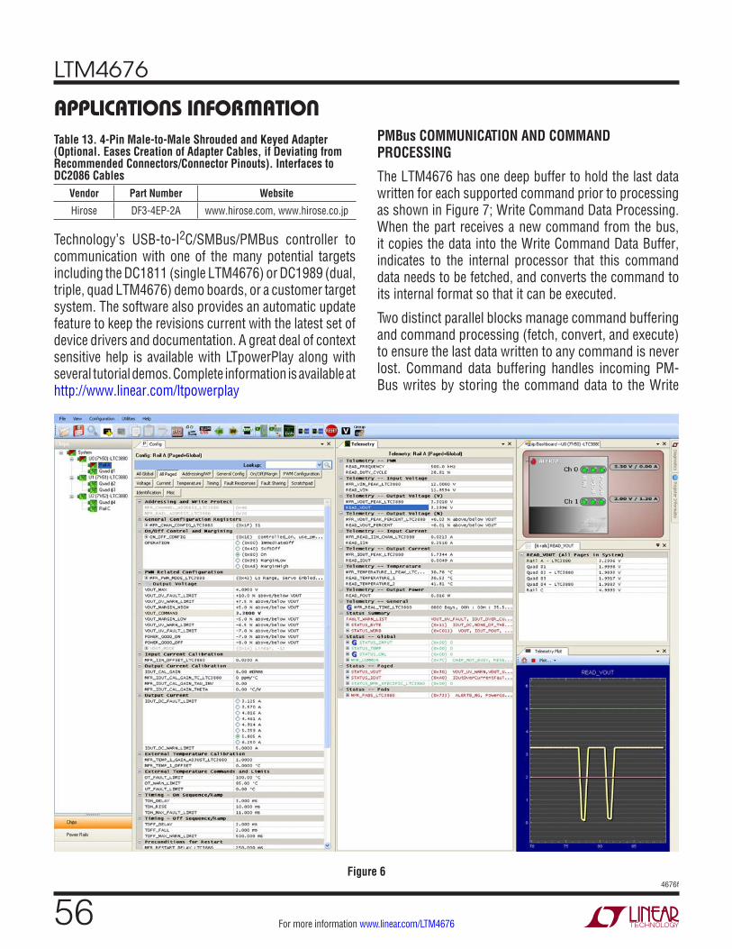
LTM4676
564676f
For more information www.linear.com/LTM4676
APPLICATIONS INFORMATION
Technology’s USB-to-I2C/SMBus/PMBus controller to communication with one of the many potential targets including the DC1811 (single LTM4676) or DC1989 (dual, triple, quad LTM4676) demo boards, or a customer target system. The software also provides an automatic update feature to keep the revisions current with the latest set of device drivers and documentation. A great deal of context sensitive help is available with LTpowerPlay along with several tutorial demos. Complete information is available at http://www.linear.com/ltpowerplay
Table 13. 4-Pin Male-to-Male Shrouded and Keyed Adapter (Optional. Eases Creation of Adapter Cables, if Deviating from Recommended Connectors/Connector Pinouts). Interfaces to DC2086 Cables
Vendor Part Number Website
Hirose DF3-4EP-2A www.hirose.com, www.hirose.co.jp
Figure 6
PMBus COMMUNICATION AND COMMAND PROCESSING
The LTM4676 has one deep buffer to hold the last data written for each supported command prior to processing as shown in Figure 7; Write Command Data Processing. When the part receives a new command from the bus, it copies the data into the Write Command Data Buffer, indicates to the internal processor that this command data needs to be fetched, and converts the command to its internal format so that it can be executed.
Two distinct parallel blocks manage command buffering and command processing (fetch, convert, and execute) to ensure the last data written to any command is never lost. Command data buffering handles incoming PM-Bus writes by storing the command data to the Write

LTM4676
574676f
For more information www.linear.com/LTM4676
APPLICATIONS INFORMATION
Command Data Buffer and marking these commands for future processing. The internal processor runs in parallel and handles the sometimes slower task of fetching, con-verting and executing commands marked for processing.
Some computationally intensive commands (e.g., timing parameters, temperatures, voltages and currents) have internal processor execution times that may be long relative to PMBus timing. If the part is busy processing a command, and new command(s) arrive, execution may be delayed or processed in a different order than received. The part indicates when internal calculations are in process via bit 5 of MFR_COMMON (‘calculations not pending’). When the part is busy calculating, bit 5 is cleared. When this bit is set, the part is ready for another command. An example polling loop is provided in Figure 7 which ensures that commands are processed in order while simplifying error handling routines.
When the part receives a new command while it is busy, it will communicate this condition using standard PMBus protocol. Depending on part configuration it may either NACK the command or return all ones (0xFF) for reads. It may also generate a BUSY fault and ALERT notification, or stretch the SCL clock low. For more information refer to PMBus Specification v1.1, Part II, Section 10.8.7 and SMBus v2.0 section 4.3.3. Clock stretching can be enabled by asserting bit 1 of MFR_CONFIG_ALL. Clock stretching will only occur if enabled and the bus communication speed exceeds 100kHz.
PMBus busy protocols are well accepted standards, but can make writing system level software somewhat com-plex. The part provides three ‘hand shaking’ status bits
which reduce complexity while enabling robust system level communication.
The three hand shaking status bits are in the MFR_ COMMON register. When the part is busy executing an internal operation, it will clear bit 6 of MFR_COMMON (‘chip not busy’). When the part is busy specifically because it is in a transitional VOUT state (margining hi/lo, power off/on, moving to a new output voltage set point, etc.) it will clear bit 4 of MFR_COMMON (‘output not in transition’). When internal calculations are in process, the part will clear bit 5 of MFR_COMMON (‘calculations not pending’). These three status bits can be polled with a PMBus read byte of the MFR_COMMON register until all three bits are set. A command immediately following the status bits being set will be accepted without NACKing or generating a BUSY fault/ALERT notification. The part can NACK commands for other reasons, however, as required by the PMBus spec (for instance, an invalid command or data). An example of a robust command write algorithm for the VOUT_COMMANDn register is provided in Figure 8.
DECODER
CMD
INTERNALPROCESSOR
WRITE COMMANDDATA BUFFER
PAGE
CMDS
0x00
0x21
0xFD
4676 F07x1
•••
•••
MFR_RESET
VOUT_COMMAND
SCALCULATIONSPENDING
PMBusWRITE
R
FETCH,CONVERT
DATAAND
EXECUTE
DATAMUX
Figure 7. Write Command Data Processing
Figure 8. Example of a Command Write of VOUT_COMMAND
// wait until bits 6, 5, and 4 of MFR_COMMON are all setdo mfrCommonValue = PMBUS_READ_BYTE(0xEF); partReady = (mfrCommonValue & 0x68) == 0x68; while(!partReady)
// now the part is ready to receive the next commandPMBUS_WRITE_WORD(0x21, 0x2000); //write VOUT_COMMAND to 2V
It is recommended that all command writes (write byte, write word, etc.) be preceded with a polling loop to avoid the extra complexity of dealing with busy behavior and unwanted ALERT notification. A simple way to achieve this is to create a SAFE_WRITE_BYTE() and SAFE_WRITE_WORD() subroutine. The above polling mechanism allows your software to remain clean and simple while robustly communicating with the part. For a detailed discussion of these topics and other special cases please refer to the application note section located at www.linear.com/designtools/app_notes.
When communicating using bus speeds at or below 100kHz, the polling mechanism shown here provides a

LTM4676
584676f
For more information www.linear.com/LTM4676
APPLICATIONS INFORMATIONsimple solution that ensures robust communication without clock stretching. At bus speeds in excess of 100kHz, it is strongly recommended that the part be configured to en-able clock stretching. This requires a PMBus master that supports clock stretching. System software that detects and properly recovers from the standard PMBus NACK/BUSY faults as described in the PMBus Specification v1.1, Part II, Section 10.8.7 is required to communicate above 100kHz without clock stretching.
THERMAL CONSIDERATIONS AND OUTPUT CURRENT DERATING
The thermal resistances reported in the Pin Configuration section of this data sheet are consistent with those pa-rameters defined by JESD51-12 and are intended for use with finite element analysis (FEA) software modeling tools that leverage the outcome of thermal modeling, simula-tion, and correlation to hardware evaluation performed on a µModule package mounted to a hardware test board defined by JESD51-9 (“Test Boards for Area Array Surface Mount Package Thermal Measurements”). The motivation for providing these thermal coefficients is found in JESD 51-12 (“Guidelines for Reporting and Using Electronic Package Thermal Information”).
Many designers may opt to use laboratory equipment and a test vehicle such as the demo board to predict the µModule regulator’s thermal performance in their application at various electrical and environmental operating conditions to compliment any FEA activities. Without FEA software, the thermal resistances reported in the Pin Configuration section are in-and-of themselves not relevant to providing guidance of thermal performance; instead, the derating curves provided later in this data sheet can be used in a manner that yields insight and guidance pertaining to one’s application-usage, and can be adapted to correlate thermal performance to one’s own application.
The Pin Configuration section gives four thermal coeffi-cients explicitly defined in JESD 51-12; these coefficients are quoted or paraphrased below:
1 θJA, the thermal resistance from junction to ambient, is the natural convection junction-to-ambient air thermal resistance measured in a one cubic foot sealed enclo-sure. This environment is sometimes referred to as “still air” although natural convection causes the air to move. This value is determined with the part mounted to a JESD 51-9 defined test board, which does not reflect an actual application or viable operating condition.
2 θJCbottom, the thermal resistance from junction to the bottom of the product case, is determined with all of the component power dissipation flowing through the bottom of the package. In the typical µModule regulator, the bulk of the heat flows out the bottom of the pack-age, but there is always heat flow out into the ambient environment. As a result, this thermal resistance value may be useful for comparing packages but the test conditions don’t generally match the user’s application.
3 θJCtop, the thermal resistance from junction to top of the product case, is determined with nearly all of the component power dissipation flowing through the top of the package. As the electrical connections of the typical µModule regulator are on the bottom of the package, it is rare for an application to operate such that most of the heat flows from the junction to the top of the part. As in the case of θJCbottom, this value may be useful for comparing packages but the test conditions don’t generally match the user’s application.
4 θJB, the thermal resistance from junction to the printed circuit board, is the junction-to-board thermal resis-tance where almost all of the heat flows through the bottom of the µModule regulator and into the board, and is really the sum of the θJCbottom and the thermal resistance of the bottom of the part through the solder joints and through a portion of the board. The board temperature is measured a specified distance from the package, using a two sided, two layer board. This board is described in JESD 51-9.

LTM4676
594676f
For more information www.linear.com/LTM4676
APPLICATIONS INFORMATIONA graphical representation of the aforementioned ther-mal resistances is given in Figure 9; blue resistances are contained within the µModule regulator, whereas green resistances are external to the µModule package.
As a practical matter, it should be clear to the reader that no individual or sub-group of the four thermal resistance parameters defined by JESD 51-12 or provided in the Pin Configuration section replicates or conveys normal operating conditions of a µModule regulator. For example, in normal board-mounted applications, never does 100% of the device’s total power loss (heat) thermally conduct exclusively through the top or exclusively through bot-tom of the µModule package—as the standard defines for θJCtop and θJCbottom, respectively. In practice, power loss is thermally dissipated in both directions away from the package—granted, in the absence of a heat sink and airflow, a majority of the heat flow is into the board.
Within the LTM4676, be aware there are multiple power devices and components dissipating power, with a con-sequence that the thermal resistances relative to different junctions of components or die are not exactly linear with respect to total package power loss. To reconcile this complication without sacrificing modeling simplicity—but also, not ignoring practical realities—an approach has been taken using FEA software modeling along with laboratory testing in a controlled-environment chamber to reason-ably define and correlate the thermal resistance values supplied in this data sheet: (1) Initially, FEA software is used to accurately build the mechanical geometry of the LTM4676 and the specified PCB with all of the correct
material coefficients along with accurate power loss source definitions; (2) this model simulates a software-defined JEDEC environment consistent with JSED 51-9 and JESD 51-12 to predict power loss heat flow and temperature readings at different interfaces that enable the calculation of the JEDEC-defined thermal resistance values; (3) the model and FEA software is used to evaluate the LTM4676 with heat sink and airflow; (4) having solved for and analyzed these thermal resistance values and simulated various operating conditions in the software model, a thorough laboratory evaluation replicates the simulated conditions with thermocouples within a controlled envi-ronment chamber while operating the device at the same power loss as that which was simulated. The outcome of this process and due diligence yields the set of derating curves provided in later sections of this data sheet, along with well-correlated JESD51-12-defined θ values provided in the Pin Configuration section of this data sheet.
The 1V, 1.8V and 3.3V power loss curves in Figures 10, 11 and 12 respectively can be used in coordination with the load current derating curves in Figures 13 to 30 for calculating an approximate θJA thermal resistance for the LTM4676 with various heat sinking and air flow conditions. These thermal resistances represent demonstrated performance of the LTM4676 on DC1543 hardware; a 4-layer FR4 PCB measuring 99mm × 113mm × 1.6mm using outer and inner copper weights of 2oz and 1oz, respectively. The power loss curves are taken at room temperature, and are increased with multiplicative factors with ambient temperature. These approximate factors are listed in Table 14.
4676 F09
µMODULE DEVICE
JUNCTION-TO-CASE (TOP)RESISTANCE
JUNCTION-TO-BOARD RESISTANCE
JUNCTION-TO-AMBIENT RESISTANCE (JESD 51-9 DEFINED BOARD)
CASE (TOP)-TO-AMBIENTRESISTANCE
BOARD-TO-AMBIENTRESISTANCE
JUNCTION-TO-CASE(BOTTOM) RESISTANCE
JUNCTION AMBIENT
CASE (BOTTOM)-TO-BOARDRESISTANCE
Figure 9. Graphical Representation of JESD51-12 Thermal Coefficients

LTM4676
604676f
For more information www.linear.com/LTM4676
APPLICATIONS INFORMATION(Compute the factor by interpolation, for intermediate temperatures.) The derating curves are plotted with the LTM4676’s paralleled outputs initially sourcing up to 26A and the ambient temperature at 30°C. The output voltages are 1V, 1.8V and 3.3V. These are chosen to include the lower and higher output voltage ranges for correlating the thermal resistance. Thermal models are derived from several temperature measurements in a controlled temperature chamber along with thermal modeling analysis. The junction temperatures are monitored while ambient temperature is increased with and without air flow, and with and without a heat sink attached with thermally conductive adhesive tape. The BGA heat sinks evaluated in Table 18 (and attached to the LTM4676 with thermally conductive adhesive tape listed in Table 19) yield very comparable performance in laminar airflow despite being visibly different in construction and form factor. The power loss increase with ambient temperature change is factored into the derating curves. The junctions are maintained at 120°C maximum while lowering output current or power while increasing ambient temperature. The decreased output current decreases the internal module loss as ambient temperature is increased. The monitored junction temperature of 120°C minus the ambient operating temperature specifies how much module temperature rise can be allowed. As an example in Figure 14, the load current is derated to ~19A at ~80°C ambient with no air or heat sink and the room temperature (25°C) power loss for this 12VIN to 1VOUT at 19AOUT condition is ~4W. A 4.8W loss is calculated by multiplying the ~4W room temperature loss from the 12VIN to 1VOUT power loss curve at 19A (Figure 10),
with the 1.2 multiplying factor at 80°C ambient (from Table 14). If the 80°C ambient temperature is subtracted from the 120°C junction temperature, then the difference of 40°C divided by 4.8W yields a thermal resistance, θJA, of 8.3°C/W—in good agreement with Table 15. Tables 15, 16 and 17 provide equivalent thermal resistances for 1V, 1.8V and 3.3V outputs with and without air flow and heat sinking. The derived thermal resistances in Tables 15, 16 and 17 for the various conditions can be multiplied by the calculated power loss as a function of ambient temperature to derive temperature rise above ambient, thus maximum junction temperature. Room temperature power loss can be derived from the efficiency curves in the Typical Performance Characteristics section and adjusted with the above ambient temperature multiplicative factors.
Table 14. Power Loss Multiplicative Factors vs Ambient Temperature
AMBIENT TEMPERATUREPOWER LOSS MULTIPLICATIVE
FACTOR
Up to 40°C 1.00
50°C 1.05
60°C 1.10
70°C 1.15
80°C 1.20
90°C 1.25
100°C 1.30
110°C 1.35
120°C 1.40

LTM4676
614676f
For more information www.linear.com/LTM4676
APPLICATIONS INFORMATIONTable 15. 1.0V OutputDERATING CURVE VIN (V) POWER LOSS CURVE AIRFLOW (LFM) HEAT SINK θJA (°C/W)Figures 13, 14, 15 5, 12, 24 Figure 10 0 None 8.5Figures 13, 14, 15 5, 12, 24 Figure 10 200 None 9.5Figures 13, 14, 15 5, 12, 24 Figure 10 400 None 10.6Figures 16, 17, 18 5, 12, 24 Figure 10 0 BGA Heat Sink 7.1Figures 16, 17, 18 5, 12, 24 Figure 10 200 BGA Heat Sink 8.2Figures 16, 17, 18 5, 12, 24 Figure 10 400 BGA Heat Sink 9.8
Table 16. 1.8V OutputDERATING CURVE VIN (V) POWER LOSS CURVE AIRFLOW (LFM) HEAT SINK θJA (°C/W)Figures 19, 20, 21 5, 12, 24 Figure 11 0 None 8.4Figures 19, 20, 21 5, 12, 24 Figure 11 200 None 9.4Figures 19, 20, 21 5, 12, 24 Figure 11 400 None 10.7Figures 22, 23, 24 5, 12, 24 Figure 11 0 BGA Heat Sink 7.1Figures 22, 23, 24 5, 12, 24 Figure 11 200 BGA Heat Sink 8.3Figures 22, 23, 24 5, 12, 24 Figure 11 400 BGA Heat Sink 9.9
Table 17. 3.3V OutputDERATING CURVE VIN (V) POWER LOSS CURVE AIRFLOW (LFM) HEAT SINK θJA (°C/W)Figure 25, 26, 27 5, 12, 24 Figure 12 0 None 8.4Figure 25, 26, 27 5, 12, 24 Figure 12 200 None 9.3Figure 25, 26, 27 5, 12, 24 Figure 12 400 None 10.6Figure 28, 29, 30 5, 12, 24 Figure 12 0 BGA Heat Sink 7.3Figure 28, 29, 30 5, 12, 24 Figure 12 200 BGA Heat Sink 8.4Figure 28, 29, 30 5, 12, 24 Figure 12 400 BGA Heat Sink 10.0
Table 18. Heat Sink Manufacturer (Thermally Conductive Adhesive Tape Pre-Attached)
HEAT SINK MANUFACTURER PART NUMBER WEBSITE
Aavid Thermalloy 375424B00034G www.aavid.com
Cool Innovations 4-050503PT411 www.coolinnovations.com
Wakefield Engineering LTN20069 www.wakefield.com
Table 19. Thermally Conductive Adhesive Tape Vendor
THERMALLY CONDUCTIVE ADHESIVE TAPE MANUFACTURER PART NUMBER WEBSITEChomerics T411 www.chomerics.com

LTM4676
624676f
For more information www.linear.com/LTM4676
APPLICATIONS INFORMATION
VOUTn (V)
VINn (V)
REF. CIRCUIT*
COUTHn (CERAMIC OUTPUT
CAP)
COUTLn (BULK
OUTPUT CAP)
CONNECT COMPna TO COMPnb?
(INTERNAL LOOP COMP)
RTHn (EXT LOOP
COMP) (kΩ)
CTHn (EXT LOOP
COMP) (nF)
fSW (kHz)
FSWPHCFG PIN-
STRAP, RESISTOR TO SGND (Table 4)
(kΩ)
VOUTn CFG PIN-
STRAP RESISTOR TO SGND (Table 2)
(kΩ)
VTRIMnCFG PIN-
STRAP, RESISTOR TO SGND (Table 3)
(kΩ)
TRANS-IENT
DROOP (0A TO 6.5A) (mV)
PK-PK DEVI-ATION (0A TO 6.5A
TO 0A) (mV)
RECOV-ERY TIME (µs)
0.9 5 Test Ckt. 2 100µF × 7 None Yes, cf. Fig. 41 N/A N/A 350 22.6 1.65 None 42 79 45
0.9 5 Test Ckt. 2 100µF × 3 330µF No. Use RTH, CTH 4.12 2.2 350 22.6 1.65 None 91 162 40
0.9 12 Test Ckt. 1 100µF × 7 None Yes, cf. Fig. 41 N/A N/A 350 22.6 1.65 None 42 79 45
0.9 12 Test Ckt. 1 100µF × 3 330µF No. Use RTH, CTH 4.12 2.2 350 22.6 1.65 None 91 162 40
0.9 24 Test Ckt. 1 100µF × 7 None Yes, cf. Fig. 41 N/A N/A 250 32.4 1.65 None 45 85 45
0.9 24 Test Ckt. 1 100µF × 3 330µF No. Use RTH, CTH 4.12 2.2 350 22.6 1.65 None 94 165 40
1 5 Test Ckt. 2 100µF × 7 None Yes, cf. Fig. 41 N/A N/A 350 22.6 2.43 0 44 85 45
1 5 Test Ckt. 2 100µF × 3 330µF No. Use RTH, CTH 4.22 2.2 350 22.6 2.43 0 90 160 40
1 12 Test Ckt. 1 100µF × 7 None Yes, cf. Fig. 41 N/A N/A 350 22.6 2.43 0 44 85 45
1 12 Test Ckt. 1 100µF × 3 330µF No. Use RTH, CTH 4.22 2.2 350 22.6 2.43 0 90 160 40
1 24 Test Ckt. 1 100µF × 7 None Yes, cf. Fig. 41 N/A N/A 250 32.4 2.43 0 47 90 45
1 24 Test Ckt. 1 100µF × 3 330µF No. Use RTH, CTH 4.22 2.2 350 22.6 2.43 0 93 164 40
1.2 5 Test Ckt. 2 100µF × 7 None Yes, cf. Fig. 41 N/A N/A 350 22.6 3.24 0 45 85 45
1.2 5 Test Ckt. 2 100µF × 3 330µF No. Use RTH, CTH 4.42 2.2 350 22.6 3.24 0 89 149 40
1.2 12 Test Ckt. 1 100µF × 7 None Yes, cf. Fig. 41 N/A N/A 350 22.6 3.24 0 45 85 45
1.2 12 Test Ckt. 1 100µF × 3 330µF No. Use RTH, CTH 4.42 2.2 350 22.6 3.24 0 89 149 40
1.2 24 Test Ckt. 1 100µF × 7 None Yes, cf. Fig. 41 N/A N/A 350 22.6 3.24 0 48 81 45
1.2 24 Test Ckt. 1 100µF × 3 330µF No. Use RTH, CTH 4.42 2.2 350 22.6 3.24 0 92 154 40
1.5 5 Test Ckt. 2 100µF × 7 None Yes, cf. Fig. 41 N/A N/A 350 22.6 4.22 None 45 85 45
1.5 5 Test Ckt. 2 100µF × 3 330µF No. Use RTH, CTH 4.75 2.2 350 22.6 4.22 None 89 149 40
1.5 12 Test Ckt. 1 100µF × 7 None Yes, cf. Fig. 41 N/A N/A 350 22.6 4.22 None 45 85 45
1.5 12 Test Ckt. 1 100µF × 3 330µF No. Use RTH, CTH 4.75 2.2 350 22.6 4.22 None 89 149 40
1.5 24 Test Ckt. 1 100µF × 7 None Yes, cf. Fig. 41 N/A N/A 425 18.0 4.22 None 48 91 45
1.5 24 Test Ckt. 1 100µF × 3 330µF No. Use RTH, CTH 4.75 2.2 350 22.6 4.22 None 93 156 40
1.8 5 Test Ckt. 2 100µF × 7 None Yes, cf. Fig. 41 N/A N/A 425 18.0 6.34 0 45 85 45
1.8 5 Test Ckt. 2 100µF × 3 330µF No. Use RTH, CTH 4.99 2.2 500 None 6.34 0 88 144 40
1.8 12 Test Ckt. 1 100µF × 7 None Yes, cf. Fig. 41 N/A N/A 500 None 6.34 0 45 85 45
1.8 12 Test Ckt. 1 100µF × 3 330µF No. Use RTH, CTH 4.99 2.2 500 None 6.34 0 88 144 40
1.8 24 Test Ckt. 1 100µF × 7 None Yes, cf. Fig. 41 N/A N/A 500 None 6.34 0 48 92 45
1.8 24 Test Ckt. 1 100µF × 3 330µF No. Use RTH, CTH 4.99 2.2 500 None 6.34 0 94 158 40
Table 20. LTM4676 Channel Output Voltage Response vs Component Matrix. 6.5A Load-Stepping at 6.5A/µs. Typical Measured Values
COUTH VENDORS PART NUMBERCOUTL VENDORS PART NUMBER
AVX 12106D107MAT2A (100μF, 6.3V, 1210 Case Size) Sanyo POSCAP 6TPF330M9L (470μF, 6.3V, 9mΩ ESR, D3L Case Size)
Murata GRM32ER60J107ME20L (100μF, 6.3V, 1210 Case Size) Sanyo POSCAP 6TPD470M (470μF, 6.3V, 10mΩ ESR, D4D Case Size)
Taiyo Yuden JMK325BJ107MM-T (100μF, 6.3V, 1210 Case Size) Sanyo POSCAP 2R5TPE470M9 (470μF, 2.5V, 9mΩ ESR, D2E Case Size)
TDK C3225X5R0J107MT (100μF, 6.3V, 1210 Case Size)

LTM4676
634676f
For more information www.linear.com/LTM4676
APPLICATIONS INFORMATION
Figure 10. 1VOUT Power Loss Curve Figure 11. 1.8VOUT Power Loss Curve Figure 12. 3.3VOUT Power Loss Curve
OUTPUT CURRENT (A)0 2 4
POW
ER L
OSS
(W)
4
6
4676 F10
2
06 8 10 12 14 16 18 20 22 24 26
8
24VIN
5VIN
3
5
1
7
12VIN
OUTPUT CURRENT (A)0
POW
ER L
OSS
(W)
6
8
10
18
4676 F11
4
2
5
7
9
3
1
04 8 12 222 206 10 14 16 24 26
24VIN
5VIN
12VIN
OUTPUT CURRENT (A)0 2 4
POW
ER L
OSS
(W)
8
12
4676 F12
4
06 8 10 12 14 16 18 20 22 24 26
14
24VIN
5VIN
6
10
2
12VIN
Table 20. LTM4676 Channel Output Voltage Response vs Component Matrix. 6.5A Load-Stepping at 6.5A/µs. Typical Measured Values
VOUTn (V)
VINn (V)
REF. CIRCUIT*
COUTHn (CERAMIC OUTPUT
CAP)
COUTLn (BULK
OUTPUT CAP)
CONNECT COMPna TO COMPnb?
(INTERNAL LOOP COMP)
RTHn (EXT LOOP
COMP) (kΩ)
CTHn (EXT LOOP
COMP) (nF)
fSW (kHz)
FSWPHCFG PIN-
STRAP, RESISTOR TO SGND (Table 4)
(kΩ)
VOUTn CFG PIN-
STRAP RESISTOR TO SGND (Table 2)
(kΩ)
VTRIMnCFG PIN-
STRAP, RESISTOR TO SGND (Table 3)
(kΩ)
TRANS-IENT
DROOP (0A TO 6.5A) (mV)
PK-PK DEVI-ATION (0A TO 6.5A
TO 0A) (mV)
RECOV-ERY TIME (µs)
2.5 5 Test Ckt. 2 100µF × 7 None Yes, cf. Fig. 41 N/A N/A 425 18.0 10.7 None 46 86 45
2.5 5 Test Ckt. 2 100µF × 3 330µF No. Use RTH, CTH 5.62 2.2 575 15.4 10.7 None 89 148 40
2.5 12 Test Ckt. 1 100µF × 7 None Yes, cf. Fig. 41 N/A N/A 575 15.4 10.7 None 46 86 45
2.5 12 Test Ckt. 1 100µF × 3 330µF No. Use RTH, CTH 5.62 2.2 575 15.4 10.7 None 90 150 40
2.5 24 Test Ckt. 1 100µF × 7 None Yes, cf. Fig. 41 N/A N/A 650 12.7 10.7 None 48 94 45
2.5 24 Test Ckt. 1 100µF × 3 330µF No. Use RTH, CTH 5.62 2.2 650 12.7 10.7 None 92 154 40
3.3 5 Test Ckt. 2 100µF × 5 None Yes, cf. Fig. 41 N/A N/A 425 18.0 22.6 None 56 110 45
3.3 12 Test Ckt. 1 100µF × 5 None Yes, cf. Fig. 41 N/A N/A 650 12.7 22.6 None 60 112 45
3.3 24 Test Ckt. 1 100µF × 5 None Yes, cf. Fig. 41 N/A N/A 750 10.7 22.6 None 62 115 45
5** 12 Test Ckt. 1 100µF × 5 None Yes, cf. Fig. 41 N/A N/A 750 10.7 32.4 7.68 62 125 50
5** 24 Test Ckt. 1 100µF × 5 None Yes, cf. Fig. 41 N/A N/A 1000 9.09 32.4 7.68 65 130 50
*For all conditions: CINH input capacitance is 10µF × 3, per channel (VIN0, VIN1). CINL bulk input capacitance of 150µF is optional if VIN has very low input impedance.
**5VOUT supported on VOUT1 channel output, only. VOUT0 channel supported range of output voltage regulation is limited to 4VOUT, max.
APPLICATIONS INFORMATION-DERATING CURVES

LTM4676
644676f
For more information www.linear.com/LTM4676
Figure 19. 5V to 1.8V Derating Curve, No Heat Sink
Figure 20. 12V to 1.8V Derating Curve, No Heat Sink
Figure 21. 24V to 1.8V Derating Curve, No Heat Sink
APPLICATIONS INFORMATION-DERATING CURVES
AMBIENT TEMPERATURE (°C)30
0
MAX
IMUM
LOA
D CU
RREN
T (A
)
2
68
10
20222426
14
40 50 60 70
4676 F19
4
1618
12
80 12090 100 110
400LFM200LFM0LFM
AMBIENT TEMPERATURE (°C)30
0
MAX
IMUM
LOA
D CU
RREN
T (A
)
2
68
10
20222426
14
40 50 60 70
4676 F20
4
1618
12
80 12090 100 110
400LFM200LFM0LFM
AMBIENT TEMPERATURE (°C)30
0
MAX
IMUM
LOA
D CU
RREN
T (A
)
2
68
10
20222426
14
40 50 60 70
4676 F21
4
1618
12
80 12090 100 110
400LFM200LFM0LFM
Figure 13. 5V to 1V Derating Curve, No Heat Sink
Figure 14. 12V to 1V Derating Curve, No Heat Sink
Figure 15. 24V to 1V Derating Curve, No Heat Sink
Figure 17. 12V to 1V Derating Curve, BGA Heat Sink
Figure 16. 5V to 1V Derating Curve, BGA Heat Sink
Figure 18. 24V to 1V Derating Curve, BGA Heat Sink
AMBIENT TEMPERATURE (°C)30
0
MAX
IMUM
LOA
D CU
RREN
T (A
)
2
68
10
20222426
14
40 50 60 70
4676 F13
4
1618
12
80 12090 100 110
400LFM200LFM0LFM
AMBIENT TEMPERATURE (°C)30
0
MAX
IMUM
LOA
D CU
RREN
T (A
)2
68
10
20222426
14
40 50 60 70
4676 F14
4
1618
12
80 12090 100 110
400LFM200LFM0LFM
AMBIENT TEMPERATURE (°C)30
0
MAX
IMUM
LOA
D CU
RREN
T (A
)
2
68
10
20222426
14
40 50 60 70
4676 F15
4
1618
12
80 12090 100 110
400LFM200LFM0LFM
AMBIENT TEMPERATURE (°C)30
0
MAX
IMUM
LOA
D CU
RREN
T (A
)
2
68
10
20222426
14
40 50 60 70
4676 F16
4
1618
12
80 12090 100 110
400LFM200LFM0LFM
AMBIENT TEMPERATURE (°C)30
0
MAX
IMUM
LOA
D CU
RREN
T (A
)
2
68
10
20222426
14
40 50 60 70
4676 F17
4
1618
12
80 12090 100 110
400LFM200LFM0LFM
AMBIENT TEMPERATURE (°C)30
0
MAX
IMUM
LOA
D CU
RREN
T (A
)
2
68
10
20222426
14
40 50 60 70
4676 F18
4
1618
12
80 12090 100 110
400LFM200LFM0LFM

LTM4676
654676f
For more information www.linear.com/LTM4676
Figure 23. 12V to 1.8V Derating Curve, with Heat Sink
Figure 22. 5V to 1.8V Derating Curve, with Heat Sink
Figure 24. 24V to 1.8V Derating Curve, with Heat Sink
Figure 26. 12V to 3.3V Derating Curve, No Heat Sink
Figure 25. 5V to 3.3V Derating Curve, No Heat Sink
Figure 27. 24V to 3.3V Derating Curve, with Heat Sink
Figure 28. 5V to 3.3V Derating Curve, with Heat Sink
Figure 29. 12V to 3.3V Derating Curve, with Heat Sink
Figure 30. 24V to 3.3V Derating Curve, with Heat Sink
APPLICATIONS INFORMATION-DERATING CURVES
AMBIENT TEMPERATURE (°C)30
0
MAX
IMUM
LOA
D CU
RREN
T (A
)
2
68
10
20222426
14
40 50 60 70
4676 F22
4
1618
12
80 12090 100 110
400LFM200LFM0LFM
AMBIENT TEMPERATURE (°C)30
0
MAX
IMUM
LOA
D CU
RREN
T (A
)2
68
10
20222426
14
40 50 60 70
4676 F23
4
1618
12
80 12090 100 110
400LFM200LFM0LFM
AMBIENT TEMPERATURE (°C)30
0
MAX
IMUM
LOA
D CU
RREN
T (A
)
2
68
10
20222426
14
40 50 60 70
4676 F24
4
1618
12
80 12090 100 110
400LFM200LFM0LFM
AMBIENT TEMPERATURE (°C)30
0
MAX
IMUM
LOA
D CU
RREN
T (A
)
2
68
10
20222426
14
40 50 60 70
4676 F25
4
1618
12
80 12090 100 110
400LFM200LFM0LFM
AMBIENT TEMPERATURE (°C)30
0
MAX
IMUM
LOA
D CU
RREN
T (A
)
2
68
10
20222426
14
40 50 60 70
4676 F26
4
1618
12
80 12090 100 110
400LFM200LFM0LFM
AMBIENT TEMPERATURE (°C)30
0
MAX
IMUM
LOA
D CU
RREN
T (A
)
2
68
10
20222426
14
40 50 60 70
4676 F27
4
1618
12
80 12090 100 110
400LFM200LFM0LFM
AMBIENT TEMPERATURE (°C)30
0
MAX
IMUM
LOA
D CU
RREN
T (A
)
2
68
10
20222426
14
40 50 60 70
4676 F28
4
1618
12
80 12090 100 110
400LFM200LFM0LFM
AMBIENT TEMPERATURE (°C)30
0
MAX
IMUM
LOA
D CU
RREN
T (A
)
2
68
10
20222426
14
40 50 60 70
4676 F29
4
1618
12
80 12090 100 110
400LFM200LFM0LFM
AMBIENT TEMPERATURE (°C)30
0
MAX
IMUM
LOA
D CU
RREN
T (A
)
2
68
10
20222426
14
40 50 60 70
4676 F30
4
1618
12
80 12090 100 110
400LFM200LFM0LFM

LTM4676
664676f
For more information www.linear.com/LTM4676
APPLICATIONS INFORMATIONEMI PERFORMANCE
The SWn pin provides access to the midpoint of the power MOSFETs in LTM4676’s power stages.
Connecting an optional series RC network from SWn to GND can dampen high frequency (~30MHz+) switch node ringing caused by parasitic inductances and capacitances in the switched-current paths. The RC network is called a snubber circuit because it dampens (or “snubs”) the resonance of the parasitics, at the expense of higher power loss.
To use a snubber, choose first how much power to allocate to the task and how much PCB real estate is available to implement the snubber. For example, if PCB space al-lows a low inductance 1W resistor to be used—derated conservatively to 600mW (PSNUB)—then the capacitor in the snubber network (CSW) is computed by:
CSW =
PSNUBVINn(MAX)2 • fSW
where VINn(MAX) is the maximum input voltage that the input to the power stage (VINn) will see in the application, and fSW is the DC/DC converter’s switching frequency of operation. CSW should be NPO, C0G or X7R-type (or better) material.
The snubber resistor (RSW) value is then given by:
RSW = 5nH
CSW
The snubber resistor should be low ESL and capable of withstanding the pulsed currents present in snubber cir-cuits. A value between 0.7Ω and 4.2Ω is normal.
For ease of snubber implementation, integrated 2.2nF snubber capacitors connect to each of the LTM4676’s channel switch nodes via a low inductance path. The electrically floating ends of these snubber capacitors are made available on the SNUBn pins of the LTM4676. Us-ing the aforementioned guidance on snubber selection, a properly sized snubber resistor can be conveniently connected directly between SNUBn and GND.
EMI performance of LTM4676 (on DC1811) with and with-out a snubber is compared and contrasted in Figures 31 and 32. The snubber resistors applied to the SNUBn pins reduce EMI signal amplitude by several dBµV/m.
Figure 31. Radiated Emissions Scan of LTM4676 Producing 1VOUT at 26A, from 12VIN. DC1811 Hardware with Outputs Paralleled. No Snubbers Applied. fSW = 350kHz. Measured in a 10m Chamber. Peak Detect Method
Figure 32. Radiated Emissions Scan of LTM4676 Producing 1VOUT at 26A, from 12VIN. DC1811 Hardware with Outputs Paralleled. 1Ω (1/4W rated) Snubber Resistors Applied from SNUBn to GND. fSW = 350kHz. Measured in a 10m Chamber. Peak Detect Method
FREQUENCY (MHz)30
–10
SIGN
AL A
MPL
ITUD
E (d
B µV
/m)
0
10
30
40
50
70
4676 F32
20
60
422.4 1010226.2 618.6 814.8
FREQUENCY (MHz)30
–10
SIGN
AL A
MPL
ITUD
E (d
B µV
/m)
0
10
30
40
50
70
4676 F31
20
60
422.4 1010226.2 618.6 814.8

LTM4676
674676f
For more information www.linear.com/LTM4676
APPLICATIONS INFORMATIONSAFETY CONSIDERATIONS
The LTM4676 modules do not provide galvanic isolation from VIN to VOUT. There is no internal fuse. If required, a slow blow fuse with a rating twice the maximum input current needs to be provided to protect each unit from catastrophic failure.
The fuse or circuit breaker should be selected to limit the current to the regulator during overvoltage in case of an internal top MOSFET fault. If the internal top MOSFET fails, then turning it off will not resolve the overvoltage, thus the internal bottom MOSFET will turn on indefinitely trying to protect the load. Under this fault condition, the input volt-age will source very large currents to ground through the failed internal top MOSFET and enabled internal bottom MOSFET. This can cause excessive heat and board dam-age depending on how much power the input voltage can deliver to this system. A fuse or circuit breaker can be used as a secondary fault protector in this situation. The device does support over current and overtemperature protection.
LAYOUT CHECKLIST/EXAMPLE
The high integration of LTM4676 makes the PCB board layout very simple and easy. However, to optimize its electrical and thermal performance, some layout consid-erations are still necessary.
• Use large PCB copper areas for high current paths, including VINn, GND and VOUTn . It helps to minimize the PCB conduction loss and thermal stress.
• Place high frequency ceramic input and output capaci-tors next to the VINn, GND and VOUTn pins to minimize high frequency noise.
• Place a dedicated power ground layer underneath the module.
• To minimize the via conduction loss and reduce module thermal stress, use multiple vias for interconnection between top layer and other power layers.
• Do not put vias directly on pads, unless they are capped or plated over.
• Use a separate SGND copper plane for components connected to signal pins. Connect SGND to GND at Channel 1’s load GND sense point.
• For parallel modules, tie the VOUTn, VOSNS0+/VOSNS
– and/or VOSNS1/SGND voltage-sense differential pair lines, RUNn, GPIOn, COMPna, SYNC and SHARE_CLK pins together—as shown in Figure 38.
• Bring out test points on the signal pins for monitoring.
Figure 33 gives a good example of the recommended layout.
SGND
12
11
10
9
8
7
6
5COUT0
GND
COUT1
CIN1CIN0
VIN0 VIN1GND
GND
4
3
2
1
A B C D E F GCNTRL VOUT1
4676 F33
VOUT0H J K L M
Figure 33. Recommended PCB Layout Package Top View
VIN0 VIN1
VOUT0 VOUT1
A
12
11
10
9
8
7
6
5
4
3
2
1
B C D E F G H J K L M
GND GND
GND GND
GND

LTM4676
684676f
For more information www.linear.com/LTM4676
TYPICAL APPLICATIONS
CINH22µF×3
CINL220µF
10k×7
VIN4.5V to 5.75V
PWM CLOCK SYNCH.TIME BASE SYNCH.
• Slave Address = 1001010_R/W (0x4A)• 350kHz Switching Frequency• No GUI Configuration and No Part-Specific Programming Required Except: VIN_OFF < VIN_UV_WARN_LIMIT < VIN_ON < 4.3V In Multi-Module Systems, Configuring RAIL_ADDRESS Is Recommended
COUT100µF×14
VOUT, 1.5VADJUSTABLEUP TO 26A
VOUT0TSNS0aTSNS0bISNS0a
+
ISNS0b+
ISNS0a–
ISNS0b–
VOSNS0+
VOSNS0–
VOUT1TSNS1aTSNS1bISNS1a
+
ISNS1b+
ISNS1a–
ISNS1b–
VOSNS1SGND
VIN0VIN1SVIN
VDD33
LOADSCLSDAALERTRUN0RUN1GPIO0GPIO1SYNCSHARE_CLK
V OUT
0CFG
V TRI
M0C
FGV O
UT1C
FGV T
RIM
1CFG
INTV
CCV D
D25
SW0
SW1
SNUB
0SN
UB1
COM
P 0a
COM
P 0b
COM
P 1a
COM
P 1b
GND
WP
10.7k1%
±50ppm/°C
22.6k1%±50ppm/°C
LTM4676
4676 F34
+
2.1k1%±50ppm/°C
SMBus INTERFACE WITHPMBus COMMAND SET
ON/OFF CONTROL, FAULTMANAGEMENT, POWER
SEQUENCING
F SW
PHCF
G
ASEL
Figure 34. 26A, 1.5V Output DC/DC µModule Regulator with I2C/SMBus/PMBus Serial Interface
(35a) 5VIN, Figure 34 Circuit (35b) 12VIN, Figure 34 Circuit with INTVCC Open and VOUT Commanded to 1V
TOTAL OUTPUT CURRENT (A)0
CHAN
NEL
OUTP
UT C
URRE
NT (A
) 12
12
4676 F35a
6
2
4 8 16
0
–2
14
10
IOUT0
IOUT18
4
20 24 28TOTAL OUTPUT CURRENT (A)
0
CHAN
NEL
OUTP
UT C
URRE
NT (A
) 12
12
4676 F35b
6
2
4 8 16
0
–2
14
10
IOUT0
IOUT18
4
20 24 28
Figure 35. Current Sharing Performance of the LTM4676's Channels

LTM4676
694676f
For more information www.linear.com/LTM4676
TYPICAL APPLICATIONS
Figure 36. 13A, 1.2V and 2.5V Outputs Generated from 3.3V Power Input and Providing I2C/SMBus/PMBus Serial Interface
Figure 37. Output Voltage Margining, Figure 36 Circuit
VOUT1, 2.5VADJUSTABLEUP TO 13A
CINH22µF×3
CINL220µF
10k×9
3.3VINNOMINAL
5VLOW POWER BIAS
<100mA
PWM CLOCK SYNCH.TIME BASE SYNCH.
• Slave Address = 1001111_R/W (0x4F)• 350kHz Switching Frequency• No GUI Configuration and No Part-Specific Programming Required Except: VIN_OFF < VIN_UV_WARN_LIMIT < VIN_ON < 4.5V In Multi-Module Systems, Configuring RAIL_ADDRESS Is Recommended
COUT0100µF×7
COUT1100µF×7
VOUT0, 1.2VADJUSTABLEUP TO 13A
VOUT0TSNS0aTSNS0bISNS0a
+
ISNS0b+
ISNS0a–
ISNS0b–
VOSNS0+
VOSNS0–
VOUT1TSNS1aTSNS1bISNS1a
+
ISNS1b+
ISNS1a–
ISNS1b–
VOSNS1SGND
VIN0VIN1SVIN
VDD33
LOAD0SCLSDAALERTRUN0RUN1GPIO0GPIO1SYNCSHARE_CLK
V OUT
0CFG
V TRI
M0C
FGV O
UT1C
FGV T
RIM
1CFG
INTV
CCV D
D25
SW0
SW1
SNUB
0SN
UB1
COM
P 0a
COM
P 0b
COM
P 1a
COM
P 1b
GND
WP
22.6k1%
±50ppm/°C
3.24k1%±50ppm/°C
LTM4676
4676 F36
+
10.7k1%±50ppm/°C
SMBus INTERFACE WITHPMBus COMMAND SET
ON/OFF CONTROL, FAULTMANAGEMENT, POWER
SEQUENCING
LOAD1
F SW
PHCF
G
ASEL
(37a) PMBus Operation (Reg. 0x01): 0x80 → 0xA8 (Margin High)
(37c) PMBus Operation (Reg. 0x01): 0x80 → 0x98 (Margin Low)
(37b) PMBus Operation (Reg. 0x01): 0xA8 → 0x80 (Margin Off)
(37d) PMBus Operation (Reg. 0x01): 0x98 → 0x80 (Margin Off)
VOUT150mV/DIV
VOUT050mV/DIV
SCL5V/DIV
SDA5V/DIV
4ms/DIV 4676 F37a
VOUT150mV/DIV
VOUT050mV/DIV
SCL5V/DIV
SDA5V/DIV
4ms/DIV 4676 F37b
VOUT150mV/DIV
VOUT050mV/DIV
SCL5V/DIV
SDA5V/DIV
4ms/DIV 4676 F37c
VOUT150mV/DIV
VOUT050mV/DIV
SCL5V/DIV
SDA5V/DIV
4ms/DIV 4676 F37d
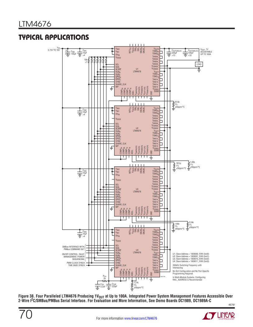
LTM4676
704676f
For more information www.linear.com/LTM4676
TYPICAL APPLICATIONS
Figure 38. Four Paralleled LTM4676 Producing 1VOUT at Up to 100A. Integrated Power System Management Features Accessible Over 2-Wire I2C/SMBus/PMBus Serial Interface. For Evaluation and More Information, See Demo Boards DC1989, DC1989A-C
CIN110µF×4
CIN5150µF
10k×7
VIN5.75V TO 16V
PWM CLOCK SYNCH.TIME BASE SYNCH.
COUT(MLCC)100µF×10
COUT(BULK)330µF×10
VOUT, 1VADJUSTABLEUP TO 100A
VOUT0TSNS0aTSNS0bISNS0a
+
ISNS0b+
ISNS0a–
ISNS0b–
VOSNS0+
VOSNS0–
VINOVIN1SVINVDD33
LOADSCLSDAALERTRUN0RUN1GPIO0GPIO1SYNCSHARE_CLK
ASEL
F SW
PHCF
GV O
UT0C
FGV T
RIM
0CFG
V OUT
1CFG
V TRI
M1C
FG
INTV
CCV D
D25
SW0
SW1
SNUB
0SN
UB1
COM
P 0a
COM
P 0b
COM
P 1a
COM
P 1b
GND
WP
22.6k1%±50ppm/°C
U1LTM4676
+
SMBus INTERFACE WITHPMBus COMMAND SET
U1: Slave Address = 1000000_R/W (0x40)U2: Slave Address = 1000001_R/W (0x41)U3: Slave Address = 1000010_R/W (0x42)U4: Slave Address = 1000011_R/W (0x43)
350kHz Switching Frequency withInterleaving
No GUI Configuration and No Part-Specific Programming Required
In Multi-Module Systems, Configuring RAIL_ADDRESS is Recommended
ON/OFF CONTROL, FAULTMANAGEMENT, POWER
SEQUENCING
CIN210µF×4
VOUT0TSNS0aTSNS0bISNS0a
+
ISNS0b+
ISNS0a–
ISNS0b–
VOSNS0+
VOSNS0–
VINOVIN1SVIN
VDD33
SCLSDAALERTRUN0RUN1GPIO0GPIO1SYNCSHARE_CLK
F SW
PHCF
GV O
UT0C
FGV T
RIM
0CFG
V OUT
1CFG
V TRI
M1C
FG
INTV
CCV D
D25
SW0
SW1
SNUB
0SN
UB1
COM
P 0a
COM
P 0b
COM
P 1a
COM
P 1b
GND
WP
1.65k1%±50ppm/°C
787Ω1%±50ppm/°C
U2LTM4676
ASEL
CIN310µF×4
VOUT0TSNS0aTSNS0bISNS0a
+
ISNS0b+
ISNS0a–
ISNS0b–
VOSNS0+
VOSNS0–
VINOVIN1SVIN
VDD33
SCLSDAALERTRUN0RUN1GPIO0GPIO1SYNCSHARE_CLK
F SW
PHCF
GV O
UT0C
FGV T
RIM
0CFG
V OUT
1CFG
V TRI
M1C
FG
INTV
CCV D
D25
SW0
SW1
SNUB
0SN
UB1
COM
P 0a
COM
P 0b
COM
P 1a
COM
P 1b
GND
WP
3.24k1%±50ppm/°C
1.65k1%±50ppm/°C
U3LTM4676
ASEL
CIN410µF×4
VOUT0TSNS0aTSNS0bISNS0a
+
ISNS0b+
ISNS0a–
ISNS0b–
VOSNS0+
VOSNS0–
VINOVIN1SVIN
VDD33
SCLSDAALERTRUN0RUN1GPIO0GPIO1SYNCSHARE_CLK
F SW
PHCF
GV O
UT0C
FGV T
RIM
0CFG
V OUT
1CFG
V TRI
M1C
FG
INTV
CCV D
D25
SW0
SW1
SNUB
0SN
UB1
COM
P 0a
COM
P 0b
COM
P 1a
COM
P 1b
GND
WP
1.21k1%±50ppm/°C
4676 F38
CTHP220pF
CTH3.3nF
RTH2k
U4LTM4676
ASEL
VOUT1TSNS1aTSNS1bISNS1a
+
ISNS1b+
ISNS1a–
ISNS1b–
VOSNS1SGND
VOUT1TSNS1aTSNS1bISNS1a
+
ISNS1b+
ISNS1a–
ISNS1b–
VOSNS1SGND
VOUT1TSNS1aTSNS1bISNS1a
+
ISNS1b+
ISNS1a–
ISNS1b–
VOSNS1SGND
VOUT1TSNS1aTSNS1bISNS1a
+
ISNS1b+
ISNS1a–
ISNS1b–
VOSNS1SGND

LTM4676
714676f
For more information www.linear.com/LTM4676
TYPICAL APPLICATIONS
Figure 39. One LTM4676 Operating In Parallel with 3xLTM4620A (See Demo Board DC2106A-A) Producing 1VOUT at up to 100A. Power System Management Features Accessible Through LTM4676 Over 2-Wire I2C/SMBus/PMBus Serial Interface. See Figure 40
CIN110µF×4
CIN5150µF
10k×6
12VIN ±20%
CIN210µF×4
COUT(MLCC)100µF×20
COUT(BULK)470µF×10
VOUT, 1VADJUSTABLEUP TO 100A
VOUT0TSNS0aTSNS0bISNS0a
+
ISNS0b+
ISNS0a–
ISNS0b–
VOSNS0+
VOSNS0–
VINOVIN1SVINVDD33
LOADSCLSDAALERTRUN0RUN1GPIO0GPIO1SYNCSHARE_CLK
ASEL
F SW
PHCF
GV O
UT0C
FGV T
RIM
0CFG
V OUT
1CFG
V TRI
M1C
FG
INTV
CCV D
D25
SW0
SW1
SNUB
0SN
UB1
COM
P 0a
COM
P 0b
COM
P 1a
COM
P 1b
GND
WP
U1LTM4676
U2LTM4620A
+
VOUT1TSNS1aTSNS1bISNS1a
+
ISNS1b+
ISNS1a–
ISNS1b–
VOSNS1SGND
PWM CLOCK SYNCH.TIME BASE SYNCH.
SMBus INTERFACE WITHPMBus COMMAND SET
ON/OFF CONTROL, FAULTMANAGEMENT, POWER
SEQUENCING
RTH51k
CTH470pF
CINTVCC24.7µF
U1: SLAVE ADDRESS = 1000000_R/W (0x40)500kHz SWITCHING FREQUENCY WITH INTERLEAVINGNO GUI CONFIGURATION AND NO PART-SPECIFICPROGRAMMING REQUIRED EXCEPT: IOUT_OC_WARN_LIMITn =18A MFR_GPIO_RESPONSEn = 0x00IN MULTI-MODULE SYSTEMS, CONFIGURINGRAIL_ADDRESS IS RECOMMENDED
RCLK200Ω
M12N7002A
1.2k1%±50ppm/°C
6.34k1%
±50ppm/°C
RTEMP2121k
RVFB8.25k
RFSET2121k
RDIV112.4k
RDIV249.9k
CIN310µF×4
CIN410µF×4
–
+U5A
1/2 LTC6244
VIN
TEMPEXTVCCPHASMD
RUN1RUN2TRACK1TRACK2
PGOOD1VOUT1
VOUTS1VFB1
VOUT2VOUTS2
VFB2
DIFFP
DIFFNDIFFOUT
MOD
E_PL
LIN
SW1
SW2
INTV
CC
CLKO
UT
SGND
GND
PGOOD2COMP1COMP2fSET
U3LTM4620A
CINTVCC34.7µF
RTEMP3121k
RFSET3121k
TEMPEXTVCCPHASMD
RUN1RUN2TRACK1TRACK2
PGOOD1VOUT1
VOUTS1VFB1
VOUT2VOUTS2
VFB2
DIFFP
DIFFNDIFFOUT
MOD
E_PL
LIN
SW1
SW2
INTV
CC
CLKO
UT
SGND
GND
PGOOD2COMP1COMP2fSET
U4LTM4620A
CINTVCC44.7µF
RTEMP4121k
RFSET4121k
TEMPEXTVCCPHASMD
RUN1RUN2TRACK1TRACK2
PGOOD1VOUT1
VOUTS1VFB1
VOUT2VOUTS2
VFB2
DIFFP
DIFFNDIFFOUT
MOD
E_PL
LIN
SW1
SW2
INTV
CC
CLKO
UT
SGND
GND
PGOOD24676 F39
COMP1COMP2fSET
–
+U5B
1/2 LTC6244

LTM4676
724676f
For more information www.linear.com/LTM4676
TYPICAL APPLICATIONS
Figure 40. Current Sharing Accuracy of Figure 39 Circuit at 12VIN
TOTAL OUTPUT CURRENT (A)0
CHAN
NEL
OUTP
UT C
URRE
NT (A
)
6
8
10
9080
4676 F40
4
2
–220 40 6010 10030 50 70
0
14
12
U1-LTM4676-IOUT0U1-LTM4676-IOUT1U2-LTM4620A-IOUT1U2-LTM4620A-IOUT2U3-LTM4620A-IOUT1U3-LTM4620A-IOUT2U4-LTM4620A-IOUT1U4-LTM4620A-IOUT2

LTM4676
734676f
For more information www.linear.com/LTM4676
PACKAGE DESCRIPTIONPACKAGE ROW AND COLUMN LABELING MAY VARY AMONG µModule PRODUCTS. REVIEW EACH PACKAGE LAYOUT CAREFULLY.
Table 21. LTM4676 BGA Pinout
PIN ID FUNCTION PIN ID FUNCTION PIN ID FUNCTION PIN ID FUNCTION PIN ID FUNCTION PIN ID FUNCTION
A1 VOUT0 B1 VOUT0 C1 VOUT0 D1 VOUT0 E1 ISNS0b– F1 ISNS0b
+
A2 VOUT0 B2 VOUT0 C2 VOUT0 D2 VOUT0 E2 ISNS0a– F2 ISNS0a
+
A3 VOUT0 B3 VOUT0 C3 VOUT0 D3 VOUT0 E3 GND F3 GND
A4 GND B4 GND C4 GND D4 GND E4 GPIO0 F4 GPIO1
A5 SNUB0 B5 GND C5 TSNS0b D5 TSNS0a E5 ALERT F5 RUN0
A6 GND B6 GND C6 GND D6 SDA E6 SCL F6 RUN1
A7 GND B7 GND C7 GND D7 GND E7 SYNC F7 SGND
A8 GND B8 GND C8 GND D8 COMP0b E8 COMP0a F8 SGND
A9 GND B9 GND C9 GND D9 VOSNS0+ E9 VOSNS0
– F9 INTVCC
A10 GND B10 SW0 C10 DNC D10 VORB0+ E10 VORB0
– F10 GND
A11 VIN0 B11 VIN0 C11 VIN0 D11 VIN0 E11 DNC F11 SVIN
A12 VIN0 B12 VIN0 C12 VIN0 D12 VIN0 E12 VIN0 F12 SVIN
PIN ID FUNCTION PIN ID FUNCTION PIN ID FUNCTION PIN ID FUNCTION PIN ID FUNCTION PIN ID FUNCTION
G1 ISNS1b– H1 ISNS1b
+ J1 VOUT1 K1 VOUT1 L1 VOUT1 M1 VOUT1
G2 ISNS1a– H2 ISNS1a
+ J2 VOUT1 K2 VOUT1 L2 VOUT1 M2 VOUT1
G3 GND H3 GND J3 VOUT1 K3 VOUT1 L3 VOUT1 M3 VOUT1
G4 ASEL H4 FSWPHCFG J4 GND K4 GND L4 GND M4 GND
G5 VOUT0CFG H5 VTRIM0CFG J5 TSNS1a K5 TSNS1b L5 GND M5 SNUB1
G6 VOUT1CFG H6 VTRIM1CFG J6 VDD25 K6 WP L6 GND M6 GND
G7 SGND H7 SHARE_CLK J7 VDD33 K7 GND L7 GND M7 GND
G8 SGND H8 COMP1a J8 COMP1b K8 GND L8 GND M8 GND
G9 INTVCC H9 VOSNS1 J9 VORB1 K9 GND L9 GND M9 GND
G10 GND H10 GND J10 GND K10 DNC L10 SW1 M10 GND
G11 GND H11 DNC J11 VIN1 K11 VIN1 L11 VIN1 M11 VIN1
G12 GND H12 VIN1 J12 VIN1 K12 VIN1 L12 VIN1 M12 VIN1

LTM4676
744676f
For more information www.linear.com/LTM4676
PACKAGE DESCRIPTION
PACKAGE PHOTOGRAPH
VOUT0
VOUT0
ISNS0b–
ISNS1b– ISNS1a
–
ISNS1b+ ISNS1a
+ FSWPHCFG
ISNS0a–
GPIO0
GPIO1ISNS0b+ ISNS0a
+
1 2 3 4 5 6 7TOP VIEW
8 9 10 11 12
M
L
K
J
H
G
F
E
D
C
B
AVIN0
VIN0
GND
GNDGND
SW0GND
SNUB0
TSNS0b
TSNS0a
RUN0
ALERT
DNC
GND COMP0b VOSNS0+
VORB0– DNC
SVIN SVIN
VORB0+
VOSNS0–COMP0aSYNC
SDA
SCL
RUN1
SGND INTVCC
GNDGND
GND ASEL VOUT0CFG
VTRIM0CFG VTRIM1CFG SHARE_CLK COMP1a VOSNS1
VOUT1CFG
GNDGND
GND DNC
VOUT1
TSNS1a
TSNS1b WP DNC
SW1
VDD25 VDD33 COMP1b VORB1
VOUT1 SNUB1
VIN1
VIN1

LTM4676
754676f
For more information www.linear.com/LTM4676
Information furnished by Linear Technology Corporation is believed to be accurate and reliable. However, no responsibility is assumed for its use. Linear Technology Corporation makes no representa-tion that the interconnection of its circuits as described herein will not infringe on existing patent rights.
PACKAGE DESCRIPTIONPlease refer to http://www.linear.com/designtools/packaging/ for the most recent package drawings.
BGA
Pack
age
144-
Lead
(16m
m ×
16m
m ×
5.0
1mm
)(R
efer
ence
LTC
DW
G #
05-0
8-19
20 R
ev B
)
PACK
AGE
TOP
VIEW
4
PIN
“A1”
CORN
ER
X
Y
aaa
Z
aaa Z
PACK
AGE
BOTT
OM V
IEW
3
SEE
NOTE
S
D
E
b
e
e
b
F
G
BGA
144
0213
REV
B
TRAY
PIN
1BE
VEL
PACK
AGE
IN T
RAY
LOAD
ING
ORIE
NTAT
ION
COM
PONE
NTPI
N “A
1”
LTM
XXXX
XXµM
odul
e
DETA
IL A
PIN
1
1110
98
76
54
32
121
A B C D E F G H KJ L M
SUGG
ESTE
D PC
B LA
YOUT
TOP
VIEW0.0000
0.00
00
0.63
0 ±0
.025
Ø 1
44x
0.63
50
0.63
50
1.90
50
1.90
50
3.17
50
3.17
50
4.44
50
4.44
50
5.71
50
5.71
50
6.98
50
6.9850
6.9850
5.7150
5.7150
4.4450
4.4450
3.1750
3.1750
1.9050
1.9050
0.6350
0.6350
6.98
50
DETA
IL A
Øb (1
44 P
LACE
S)
A
DETA
IL B
PACK
AGE
SIDE
VIE
W
Z
MX
YZ
ddd
MZ
eee
A2
DETA
IL B
SUBS
TRAT
E
A1
b1
ccc
Z
MOL
DCA
P
SYM
BOL
A A1 A2 b b1 D E e F G H1 H2 aaa
bbb
ccc
ddd
eee
MIN
4.81
0.50
4.31
0.60
0.60
0.36
3.95
NOM
5.01
0.60
4.41
0.75
0.63
16.0
016
.00
1.27
13.9
713
.97
0.41
4.00
MAX
5.21
0.70
4.51
0.90
0.66
0.46
4.05
0.15
0.10
0.20
0.30
0.15
NOTE
S
DIM
ENSI
ONS
TOTA
L NU
MBE
R OF
BAL
LS: 1
44
// bbb Z
Z
H2H1
NOTE
S:1.
DIM
ENSI
ONIN
G AN
D TO
LERA
NCIN
G PE
R AS
ME
Y14.
5M-1
994
2. A
LL D
IMEN
SION
S AR
E IN
MIL
LIM
ETER
S
BAL
L DE
SIGN
ATIO
N PE
R JE
SD M
S-02
8 AN
D JE
P95
5. P
RIM
ARY
DATU
M -Z
- IS
SEAT
ING
PLAN
E
6. S
OLDE
R BA
LL C
OMPO
SITI
ON IS
96.
5% S
n/3.
0% A
g/0.
5% C
u
43
DETA
ILS
OF P
IN #
1 ID
ENTI
FIER
ARE
OPT
IONA
L,BU
T M
UST
BE L
OCAT
ED W
ITHI
N TH
E ZO
NE IN
DICA
TED.
THE
PIN
#1 ID
ENTI
FIER
MAY
BE
EITH
ER A
MOL
D OR
M
ARKE
D FE
ATUR
E
7PA
CKAG
E RO
W A
ND C
OLUM
N LA
BELI
NG M
AY V
ARY
AMON
G µM
odul
e PR
ODUC
TS. R
EVIE
W E
ACH
PACK
AGE
LAYO
UT C
AREF
ULLY
!
7
SEE
NOTE
S

LTM4676
764676f
For more information www.linear.com/LTM4676 LINEAR TECHNOLOGY CORPORATION 2013
LT 0813 • PRINTED IN USALinear Technology Corporation1630 McCarthy Blvd., Milpitas, CA 95035-7417(408) 432-1900 FAX: (408) 434-0507 www.linear.com/LTM4676
RELATED PARTS
TYPICAL APPLICATION
Figure 41. 13A, 1V and 13A, 1.8V Output DC/DC µModule Regulator with Serial Interface
VOUT1, 1.8VADJUSTABLEUP TO 13A
CINH22µF×3
CINL220µF
10k×9
VIN5.75V TO 26.5V
PWM CLOCK SYNCH.TIME BASE SYNCH.
• Slave Address = 1001111_R/W (0x4F)• Switching Frequency: 350kHz• No GUI Configuration and No Part Specific Programming Required In Multi-Module Systems, Configuring RAIL_ADDRESS Is Recommended
COUT0100µF×7
COUT1100µF×7
VOUT0, 1.0VADJUSTABLEUP TO 13A
VOUT0TSNS0aTSNS0bISNS0a
+
ISNS0b+
ISNS0a–
ISNS0b–
VOSNS0+
VOSNS0–
VOUT1TSNS1aTSNS1bISNS1a
+
ISNS1b+
ISNS1a–
ISNS1b–
VOSNS1SGND
VIN0VIN1SVIN
VDD33
LOAD0SCLSDAALERTRUN0RUN1GPIO0GPIO1SYNCSHARE_CLK
ASEL
F SW
PHCF
GV O
UT0C
FGV T
RIM
0CFG
V OUT
1CFG
V TRI
M1C
FG
INTV
CCV D
D25
SW0
SW1
SNUB
0SN
UB1
COM
P 0a
COM
P 0b
COM
P 1a
COM
P 1b
GND
WP
6.34k1%±50ppm/°C
LTM4676
4676 F41
+
22.6k1%
±50ppm/°C
SMBus INTERFACE WITHPMBus COMMAND SET
ON/OFF CONTROL, FAULTMANAGEMENT, POWER
SEQUENCING
LOAD1
DESIGN RESOURCESSUBJECT DESCRIPTION
µModule Design and Manufacturing Resources Design: • Selector Guides • Demo Boards and Gerber Files • Free Simulation Tools
Manufacturing: • Quick Start Guide • PCB Design, Assembly and Manufacturing Guidelines • Package and Board Level Reliability
µModule Regulator Products Search 1. Sort table of products by parameters and download the result as a spread sheet.2. Search using the Quick Power Search parametric table.
TechClip Videos Quick videos detailing how to bench test electrical and thermal performance of µModule products.
Digital Power System Management Linear Technology’s family of digital power supply management ICs are highly integrated solutions that offer essential functions, including power supply monitoring, supervision, margining and sequencing, and feature EEPROM for storing user configurations and fault logging.
PART NUMBER DESCRIPTION COMMENTS
LTM4620A Dual 13A or Single 26A Step-Down µModule Regulator 4.5V ≤ VIN ≤ 16V, 0.6V ≤ VOUT ≤ 5.3V, 15mm × 15mm × 4.41mm LGA
LTM4641 10A µModule Regulator with Advanced Input and Load Protection
4.5V ≤ VIN ≤ 38V, 0.6V ≤ VOUT ≤ 6V, 15mm × 15mm × 5.01mm BGA
LTC3880/LTC3883 Dual and Single Output DC/DC Controllers with Power System Management
0.5% TUE 16-Bit ADC, Voltage/Current/Temperature Monitoring and Supervision
LTC2977/LTC2974 8- and 4-Channel PMBus Power System Managers 0.25% TUE 16-Bit ADC, Voltage/Temperature Monitoring and Supervision


