dsPIC33FJ06GS001/101A/102A/202A and dsPIC33FJ09GS302 ...
352
2011-2012 Microchip Technology Inc. DS75018C-page 1 dsPIC33FJ06GS001/101A/102A/202A and dsPIC33FJ09GS302 Operating Conditions • 3.0V to 3.6V, -40ºC to +125ºC, DC to 40 MIPS Core: 16-Bit dsPIC33F CPU • Code Efficient (C and Assembly) Architecture • Two 40-Bit Wide Accumulators • Single-Cycle (MAC/MPY) with Dual Data Fetch • Single-Cycle Mixed-Sign MUL plus Hardware Divide • 32-Bit Multiply Support Clock Management • ±2% Internal Oscillator • Programmable PLLs and Oscillator Clock Sources • Fail-Safe Clock Monitor (FSCM) • Independent Watchdog Timer (WDT) • Fast Wake-up and Start-up Power Management • Low-Power Management modes (Sleep, Idle, Doze) • Integrated Power-on Reset and Brown-out Reset • 2.0 mA/MHz Dynamic Current (typical) • 135 μA IPD Current (typical) High-Speed PWM • Up to Three PWM Pairs with Independent Timing • Dead Time for Rising and Falling Edges • 1.04 ns PWM Resolution for Dead Time, Duty Cycle, Phase and Frequency • PWM Support for: - DC/DC, AC/DC, Inverters, PFC and Lighting • Programmable Fault Inputs • Flexible Trigger Configurations for ADC Conversions Advanced Analog Features • Two High-Speed Comparators with Direct Connection to the PWM module: - Buffered/amplified output drive - Independent 10-bit DAC for each comparator - Rail-to-rail comparator operation - DACOUT amplifier (1x, 1.8x) - Selectable hysteresis - Programmable output polarity - Interrupt generation capability Advanced Analog Features (Continued) • ADC module: - 10-bit resolution with Successive Approximation Register (SAR) converter (2 Msps) and three Sample-and-Hold (S&H) circuits - Up to 8 input channels grouped into four conversion pairs, plus two inputs for monitoring voltage references - Flexible and independent ADC trigger sources - Dedicated Result register for each analog channel Timers/Output Compare/Input Capture • Two 16-Bit General Purpose Timers/Counters • Input Capture module • Output Compare module • Peripheral Pin Select (PPS) to allow Function Remap Communication Interfaces • UART module (10 Mbps): - With support for LIN/J2602 protocols and IrDA ® • 4-Wire SPI module •I 2 C™ module (up to 1 Mbaud) with SMBus Support • PPS to allow Function Remap Input/Output • Constant Current Source: - Constant current generator (10 μA nominal) • Sink/Source 18 mA on 8 Pins and 6 mA on 13 Pins • 5V Tolerant Pins • Selectable Open-Drain and Pull-ups • External Interrupts on 16 I/O Pins Qualification and Class B Support • AEC-Q100 REVG (Grade 1, -40ºC to +125ºC) Planned • Class B Safety Library, IEC 60730 Debugger Development Support • In-Circuit and In-Application Programming • Two Breakpoints • IEEE 1149.2 Compatible (JTAG) Boundary Scan • Trace and Run-Time Watch 16-Bit Microcontrollers and Digital Signal Controllers with High-Speed PWM, ADC and Comparators
Transcript of dsPIC33FJ06GS001/101A/102A/202A and dsPIC33FJ09GS302 ...

dsPIC33FJ06GS001/101A/102A/202Aand dsPIC33FJ09GS302
16-Bit Microcontrollers and Digital Signal Controllers with High-Speed PWM, ADC and Comparators
Operating Conditions
• 3.0V to 3.6V, -40ºC to +125ºC, DC to 40 MIPS
Core: 16-Bit dsPIC33F CPU
• Code Efficient (C and Assembly) Architecture• Two 40-Bit Wide Accumulators• Single-Cycle (MAC/MPY) with Dual Data Fetch• Single-Cycle Mixed-Sign MUL plus Hardware Divide• 32-Bit Multiply Support
Clock Management
• ±2% Internal Oscillator• Programmable PLLs and Oscillator Clock Sources• Fail-Safe Clock Monitor (FSCM)• Independent Watchdog Timer (WDT)• Fast Wake-up and Start-up
Power Management• Low-Power Management modes (Sleep, Idle, Doze)• Integrated Power-on Reset and Brown-out Reset• 2.0 mA/MHz Dynamic Current (typical)• 135 µA IPD Current (typical)
High-Speed PWM• Up to Three PWM Pairs with Independent Timing• Dead Time for Rising and Falling Edges • 1.04 ns PWM Resolution for Dead Time, Duty Cycle,
Phase and Frequency• PWM Support for:
- DC/DC, AC/DC, Inverters, PFC and Lighting• Programmable Fault Inputs• Flexible Trigger Configurations for ADC Conversions
Advanced Analog Features• Two High-Speed Comparators with Direct Connection to
the PWM module:- Buffered/amplified output drive- Independent 10-bit DAC for each comparator- Rail-to-rail comparator operation- DACOUT amplifier (1x, 1.8x) - Selectable hysteresis - Programmable output polarity- Interrupt generation capability
Advanced Analog Features (Continued)• ADC module:
- 10-bit resolution with Successive Approximation Register (SAR) converter (2 Msps) and three Sample-and-Hold (S&H) circuits
- Up to 8 input channels grouped into four conversion pairs, plus two inputs for monitoring voltage references
- Flexible and independent ADC trigger sources- Dedicated Result register for each
analog channel
Timers/Output Compare/Input Capture• Two 16-Bit General Purpose Timers/Counters• Input Capture module• Output Compare module• Peripheral Pin Select (PPS) to allow Function Remap
Communication Interfaces• UART module (10 Mbps):
- With support for LIN/J2602 protocols and IrDA®
• 4-Wire SPI module• I2C™ module (up to 1 Mbaud) with SMBus Support• PPS to allow Function Remap
Input/Output• Constant Current Source:
- Constant current generator (10 µA nominal)• Sink/Source 18 mA on 8 Pins and 6 mA on 13 Pins• 5V Tolerant Pins• Selectable Open-Drain and Pull-ups• External Interrupts on 16 I/O Pins
Qualification and Class B Support• AEC-Q100 REVG (Grade 1, -40ºC to +125ºC) Planned• Class B Safety Library, IEC 60730
Debugger Development Support• In-Circuit and In-Application Programming• Two Breakpoints• IEEE 1149.2 Compatible (JTAG) Boundary Scan• Trace and Run-Time Watch
2011-2012 Microchip Technology Inc. DS75018C-page 1

dsPIC33FJ06GS001/101A/102A/202A and dsPIC33FJ09GS302
dsPIC33FJ06GS001/101A/102A/202A and dsPIC33FJ09GS302 PRODUCT FAMILIES
The device names, pin counts, memory sizes and periph-eral availability of each device are listed in Table 1. Thefollowing pages show their pinout diagrams.
TABLE 1: dsPIC33FJ06GS001/101A/102A/202A and dsPIC33FJ09GS302 PRODUCT FAMILIES
Device
Pin
s
Pro
gra
m F
lash
Mem
ory
(Kb
ytes
)
RA
M (B
ytes
)Remappable Peripherals
DA
C O
utp
ut
Co
nst
ant C
urr
ent S
ou
rce
Ref
eren
ce C
lock
I2 C™
ADC
I/O P
ins
Pac
kag
es
Rem
appa
ble
Pin
s
16-B
it Ti
mer
Inp
ut C
aptu
re
Ou
tpu
t Co
mpa
re
UA
RT
SP
I
PW
M(2
)
An
alo
g C
om
para
tor
Ext
ern
al In
terr
up
ts(1
)
SA
Rs
Sam
ple
-an
d-H
old
(S&
H) C
ircu
it
An
alo
g-t
o-D
igita
l In
pu
ts
dsPIC33FJ06GS00118
6 256 8 2 0 0 0 0 2x2 2 3 0 0 0 1 1 2 6 13
PDIP, SOIC
20 SSOP
dsPIC33FJ06GS101A18
6 256 8 2 0 1 1 1 2x2 0 3 0 0 1 1 1 3 6 13
PDIP, SOIC
20 SSOP
dsPIC33FJ06GS102A28
6 256 16 2 0 1 1 1 2x2 0 3 0 0 1 1 1 3 6 21
SPDIP, SOIC, SSOP, QFN-S
36 VTLA
dsPIC33FJ06GS202A28
6 1K 16 2 1 1 1 1 2x2 2 3 1 0 1 1 1 3 6 21
SPDIP, SOIC, SSOP, QFN-S
36 VTLA
dsPIC33FJ09GS30228
9 1K 16 2 1 1 1 1 3x2 2 3 1 1 1 1 1 3 8 21
SPDIP, SOIC, SSOP, QFN-S
36 VTLA
Note 1: INT0 is not remappable.
2: The PWM4 pair is remappable and only available on dsPIC33FJ06GS001/101A and dsPIC33FJ09GS302 devices.
DS75018C-page 2 2011-2012 Microchip Technology Inc.

dsPIC33FJ06GS001/101A/102A/202A and dsPIC33FJ09GS302
Pin Diagrams
18-Pin SOIC, PDIP
dsP
IC33F
J06GS
001
MCLR
AN0/CMP1A/RA0
AN1/CMP1B/RA1
VDD
VSS
AN2/CMP1C/CMP2A/RA2
TDO/RP5(1)/CN5/RB5 PGEC2/TMS/EXTREF/RP4(1)/CN4/RB4
PGED2/TCK/INT0/RP3(1)/CN3/RB3
VCAP
OSC2/CLKO/AN7/RP2(1)/CN2/RB2
OSC1/CLKI/AN6/RP1(1)/CN1/RB1 VSS
PGEC1/SDA1/RP7(1)/CN7/RB7
PGED1/TDI/SCL1/RP6(1)/CN6/RB6
AN3/CMP1D/CMP2B/RP0(1)/CN0/RB0
1
2
3
4
5
6
7
8
9
18
17
16
15
14
13
12
11
10
PWM1L/RA3
PWM1H/RA4
Note 1: The RPn pins can be used by any remappable peripheral. See Table 1 for the list of available peripherals.
= Pins are up to 5V tolerant
MCLR
AN0/CMP1A/RA0
AN1/CMP1B/RA1
AVDD
AVSS
AN2/CMP1C/CMP2A/RA2
TDO/RP5(1)/CN5/RB5 PGEC2/TMS/EXTREF/RP4(1)/CN4/RB4
PGED2/TCK/INT0/RP3(1)/CN3/RB3
VCAP
OSCO/CLKO/AN7/RP2(1)/CN2/RB2
OSCI/CLKI/AN6/RP1(1)/CN1/RB1 VSS
PGEC1/SDA1/RP7(1)/CN7/RB7
PGED1/TDI/SCL1/RP6(1)/CN6/RB6
AN3/CMP1D/CMP2B/RP0(1)/CN0/RB0
PWM1L/RA3
PWM1H/RA4
VDD
VSS
20-Pin SSOP = Pins are up to 5V tolerant
dsP
IC33F
J06GS
001
1
2
3
4
5
6
7
8
9
18
17
16
15
14
13
12
1110
19
20
MCLR
AN0/RA0
AN1/RA1
VDD
VSS
AN2/RA2
TDO/RP5(1)/CN5/RB5 PGEC2/TMS/RP4(1)/CN4/RB4
PGED2/TCK/INT0/RP3(1)/CN3/RB3
VCAP
OSC2/CLKO/AN7/RP2(1)/CN2/RB2
OSC1/CLKI/AN6/RP1(1)/CN1/RB1 VSS
PGEC1/SDA1/RP7(1)/CN7/RB7
PGED1/TDI/SCL1/RP6(1)/CN6/RB6
AN3/RP0(1)/CN0/RB0
1
2
3
4
5
6
7
8
9
18
17
16
15
14
13
12
11
10
PWM1L/RA3
PWM1H/RA4d
sPIC
33FJ06G
S1
01A
MCLR
AN0/RA0
AN1/RA1
AVDD
AVSS
AN2/RA2
TDO/RP5(1)/CN5/RB5 PGEC2/TMS/RP4(1)/CN4/RB4
PGED2/TCK/INT0/RP3(1)/CN3/RB3
VCAP
OSCO/CLKO/AN7/RP2(1)/CN2/RB2
OSCI/CLKI/AN6/RP1(1)/CN1/RB1 VSS
PGEC1/SDA1/RP7(1)/CN7/RB7
PGED1/TDI/SCL1/RP6(1)/CN6/RB6
AN3/RP0(1)/CN0/RB0
PWM1L/RA3
PWM1H/RA4
VDD
VSS
1
2
3
4
5
6
7
8
9
18
17
16
15
14
13
12
1110
19
20
dsP
IC33F
J06GS
101A
2011-2012 Microchip Technology Inc. DS75018C-page 3

dsPIC33FJ06GS001/101A/102A/202A and dsPIC33FJ09GS302
Pin Diagrams (Continued)
28-Pin SPDIP, SOIC, SSOP
dsP
IC33F
J09GS
302
MCLR
PWM1L/RA3PWM1H/RA4PWM2L/RP14(1)/CN14/RB14PWM2H/RP13(1)/CN13/RB13TCK/RP12(1)/CN12/RB12TMS/RP11(1)/CN11/RB11VSS
VDD
AN0/CMP1A/RA0AN1/CMP1B1/RA1
AVDD
AVSS
AN2/CMP1C/CMP2A/RA2
PGED3/RP8(1)/CN8/RB8 PGEC3/RP15/CN15/RB15
PGEC2/EXTREF/RP4(1)/CN4/RB4PGED2/DACOUT/INT0/RP3(1)/CN3/RB3
VCAP
OSC2/CLKO/AN7/ISRC1/RP2(1)/CN2/RB2OSC1/CLKI/AN6/ISRC2/RP1(1)/CN1/RB1
VSS
TDO/RP5(1)/CN5/RB5
PGEC1/SDA1/RP7(1)/CN7/RB7PGED1/TDI/SCL1/RP6(1)/CN6/RB6
AN5/ISRC3/CMP2D/RP10(1)/CN10/RB10AN4/ISRC4/CMP2C/RP9(1)/CN9/RB9
AN3/CMP1D/CMP2B/RP0(1)/CN0/RB0
1234567891011121314
2827262524232221201918171615
= Pins are up to 5V tolerant
28-Pin SOIC, SPDIP, SSOP
dsP
IC33F
J06GS
102A
MCLR
PWM1L/RA3PWM1H/RA4PWM2L/RP14(1)/CN14/RB14PWM2H/RP13(1)/CN13/RB13TCK/RP12(1)/CN12/RB12TMS/RP11(1)/CN11/RB11VSS
VDD
AN0/RA0 AN1/RA1
AVDD
AVSS
AN2/RA2
PGED3/RP8(1)/CN8/RB8 PGEC3/RP15(1)/CN15/RB15
PGEC2/RP4(1)/CN4/RB4PGED2/INT0/RP3(1)/CN3/RB3
VCAPOSC2/CLKO/RP2(1)/CN2/RB2OSC1/CLKI/RP1(1)/CN1/RB1
VSS
TDO/RP5(1)/CN5/RB5
PGEC1/SDA1/RP7(1)/CN7/RB7PGED1/TDI/1SCL1/RP6(1)/CN6/RB6
AN5/RP10(1)/CN10/RB10AN4/RP9(1)/CN9/RB9AN3/RP0(1)/CN0/RB0
1234567891011121314
2827262524232221201918171615
28-Pin SPDIP, SOIC, SSOP
dsP
IC33
FJ06G
S202A
MCLR
PWM1L/RA3PWM1H/RA4PWM2L/RP14(1)/CN14/RB14PWM2H/RP13(1)/CN13/RB13TCK/RP12(1)/CN12/RB12TMS/RP11(1)/CN11/RB11VSS
VDD
AN0/CMP1A/RA0 AN1/CMP1B/RA1
AVDD
AVSS
AN2/CMP1C/CMP2A/RA2
PGED3/RP8(1)/CN8/RB8 PGEC3/RP15(1)/CN15/RB15
PGEC2/EXTREF/RP4(1)/CN4/RB4PGED2/DACOUT/INT0/RP3(1)/CN3/RB3
VCAPOSC2/CLKO/RP2(1)/CN2/RB2OSC1/CLKI/RP1(1)/CN1/RB1
VSS
TDO/RP5(1)/CN5/RB5
PGEC1/SDA1/RP7(1)/CN7/RB7PGED1/TDI/SCL1/RP6(1)/CN6/RB6
AN5/CMP2D/RP10(1)/CN10/RB10AN4/CMP2C/RP9(1)/CN9/RB9
AN3/CMP1D/CMP2B/RP0(1)/CN0/RB0
1234567891011121314
2827262524232221201918171615
= Pins are up to 5V tolerant
= Pins are up to 5V tolerant
Note 1: The RPn pins can be used by any remappable peripheral. See Table 1 for the list of available peripherals.
DS75018C-page 4 2011-2012 Microchip Technology Inc.

dsPIC33FJ06GS001/101A/102A/202A and dsPIC33FJ09GS302
Pin Diagrams (Continued)
28-Pin QFN-S(2)
10 11
23
6
1
18192021
22
12 13 1415
87
1617
232425262728
9
dsPIC33FJ06GS102A
PG
ED
2/I
NT
0/R
P3
(1) /C
N3
/RB
3
54
AV
DD
AV
SS
PW
M1L
/RA
3P
WM
1H/R
A4
PWM2L/RP14(1)/CN14/RB14PWM2H/RP13(1)/CN13/RB13TCK/RP12(1)/CN12/RB12TMS/RP11(1)/CN11/RB11
VSS
VCAP
PGEC1/SDA1/RP7(1)/CN7/RB7
PG
ED
1/T
DI/
SC
L1
/RP
6(1
) /CN
6/R
B6
TD
O/R
P5
(1) /C
N5
/RB
5
PG
EC
3/R
P1
5(1) /C
N15
/RB
15
MC
LR
AN
0/R
A0
AN
1/R
A1
AN2/RA2
AN3/RP0(1)/CN0/RB0AN4/RP9(1)/CN9/RB9
AN5/RP10(1)/CN10/RB10VSS
OSC1/CLKI/RP1(1)/CN1/RB1OSC2/CLKO/RP2(1)/CN2/RB2
PG
EC
2/R
P4
(1) /C
N4
/RB
4V
DD
PG
ED
3/R
P8
(1) /C
N8
/RB
8
10 11
2
3
6
1
18
19
20
21
22
12 13 1415
87
16
17
232425262728
9
dsPIC33FJ06GS202A
PG
ED
2/D
AC
OU
T/I
NT
0/R
P3(1
) /CN
3/R
B3
5
4
AV
DD
AV
SS
PW
M1L
/RA
3
PW
M1H
/RA
4
PWM2L/RP14(1)/CN14/RB14
PWM2H/RP13(1)/CN13/RB13
TCK/RP12(1)/CN12/RB12
TMS/RP11(1)/CN11/RB11
VSS
VCAP
PGEC1/SDA1/RP7(1)/CN7/RB7
PG
ED
1/T
DI/
SC
L1
/RP
6(1) /C
N6
/RB
6
TD
O/R
P5(1
) /CN
5/R
B5
PG
EC
3/R
P1
5(1
) /CN
15
/RB
15
MC
LR
AN
0/C
MP
1A
/RA
0
AN
1/C
MP
1B
/RA
1
AN2/CMP1C/CMP2A/RA2
AN3/CMP1D/CMP2B/RP0(1)/CN0/RB0
AN4/CMP2C/RP9(1)/CN9/RB9
AN5/CMP2D/RP10(1)/CN10/RB10
VSS
OSC1/CLKI/RP1(1)/CN1/RB1
OSC2/CLKO/RP2(1)/CN2/RB2
PG
EC
2/E
XT
RE
F/R
P4(1
) /CN
4/R
B4
VD
D
PG
ED
3/R
P8(1
) /CN
8/R
B8
Note 1: The RPn pins can be used by any remappable peripheral. See Table 1 for the list of available peripherals.2: The metal plane at the bottom of the device is not connected to any pins and is recommended to be connected to
VSS externally.
= Pins are up to 5V tolerant
= Pins are up to 5V tolerant 28-Pin QFN-S(2)
2011-2012 Microchip Technology Inc. DS75018C-page 5

dsPIC33FJ06GS001/101A/102A/202A and dsPIC33FJ09GS302
Pin Diagrams (Continued)
28-Pin QFN-S(2)
10 11
23
6
1
18192021
22
12 13 1415
87
1617
232425262728
9
dsPIC33FJ09GS302
PG
ED
2/D
AC
OU
T/IN
T0
/RP
3(1) /C
N3
/RB
3
54
AV
DD
AV
SS
PW
M1L
/RA
3
PW
M1H
/RA
4
PWM2L/RP14(1)/CN14/RB14PWM2H/RP13(1)/CN13/RB13
TCK/RP12(1)/CN12/RB12TMS/RP11(1)/CN11/RB11
VSS
VCAP
PGEC1/SDA1/RP7(1)/CN7/RB7
PG
ED
1/T
DI/
SC
L1
/RP
6(1) /C
N6
/RB
6
TD
O/R
P5(1
) /CN
5/R
B5
PG
EC
3/R
P1
5(1
) /CN
15
/RB
15
MC
LR
AN
0/C
MP
1A/R
A0
AN
1/C
MP
1B/R
A1
AN2/CMP1C/CMP2A/RA2
AN3/CMP1D/CMP2B/RP0(1)/CN0/RB0AN4/ISRC4/CMP2C/RP9(1)/CN9/RB9
AN5/ISRC3/CMP2D/RP10(1)/CN10/RB10VSS
OSC1/CLKI/AN6/ISRC2/RP1(1)/CN1/RB1OSC2/CLKO/AN7/ISRC1//RP2(1)/CN2/RB2
PG
EC
2/E
XT
RE
F/R
P4(1
) /CN
4/R
B4
VD
D
PG
ED
3/R
P8(1
) /CN
8/R
B8
Note 1: The RPn pins can be used by any remappable peripheral. See Table 1 for the list of available peripherals.2: The metal plane at the bottom of the device is not connected to any pins and is recommended to be connected to
VSS externally.
= Pins are up to 5V tolerant
DS75018C-page 6 2011-2012 Microchip Technology Inc.

dsPIC33FJ06GS001/101A/102A/202A and dsPIC33FJ09GS302
Pin Diagrams (Continued)
36-Pin VTLA
Note 1: The RPn pins can be used by any remappable peripheral. See Table 1 for the list of available peripherals.
2: The metal pad at the bottom of the device is not connected to any pins and is recommended to be connected to VSS externally.
1
dsPIC33FJ06GS102A
10
33 32 31 30 29 28
2
3
4
5
6
24
23
22
21
20
19
11 12 13 14 15
AN
1/R
A1
AN
2/R
A2
AN
3/R
P0(1
) /CN
0/R
B0
MC
LR
AV
DD
PW
M1L
/RA
3
RM
W1H
/RA
4
AV
SS
AN
0/R
A0
N/C
VSS
PGEC1/SDA1/RP7(1)/CN7/RB7
PWM2L/RP14(1)/CN14/RB14
PWM2H/RP13(1)/CN13/RB13
TMS/RP11(1)/CN11/RB11
TCK/RP12(1)/CN12/RB12
VDD
VCAPVDD
AN4/RP9(1)/CN9/RB9
NC
OSCO/CLKO/RP2(1)/CN2/RB2
NC
NC
AN5/RP10(1)/CN10/RB10
VSS
OSCI/CLKI/RP1(1)/CN1/RB1
VS
S
PG
EC
2/R
P4(1
) /CN
4/R
B4
PG
ED
3/R
P8(1
) /CN
8/R
B8
PG
ED
2/IN
T0/
RP
3(1) /C
N3/
RB
3
PG
EC
3/R
P15
(1) /C
N15
/RB
15
TD
O/R
P5(1
) /CN
5/R
B5
PG
ED
1/T
DI/S
CL1
/RP
6(1) /C
N6/
RB
6
VD
D
VD
D
7
8
9
343536
16 17 18
27
26
25
= Pins are up to 5V tolerant
2011-2012 Microchip Technology Inc. DS75018C-page 7

dsPIC33FJ06GS001/101A/102A/202A and dsPIC33FJ09GS302
Pin Diagrams (Continued)
36-Pin VTLA
Note 1: The RPn pins can be used by any remappable peripheral. See Table 1 for the list of available peripherals.2: The metal pad at the bottom of the device is not connected to any pins and is recommended to be connected
to VSS externally.
1
dsPIC33FJ06GS202A
10
33 32 31 30 29 28
2
3
4
5
6
24
23
22
21
20
19
11 12 13 14 15
AN
1/C
MP
1B/R
A1
AN
2/C
MP
1C/C
MP
2A/R
A2
AN
3/C
MP
1D/C
MP
2B/R
P0(1
) /CN
0/R
B0
MC
LR
AV
DD
PW
M1L
/RA
3
RM
W1H
/RA
4
AV
SS
AN
0/C
MP
1A/R
A0
N/C
VSS
PGEC1/SDA1/RP7(1)/CN7/RB7
PWM2L/RP14(1)/CN14/RB14
PWM2H/RP13(1)/CN13/RB13
TMS/RP11(1)/CN11/RB11
TCK/RP12(1)/CN12/RB12
VDD
VCAPVDD
AN4/CMP2C/RP9(1)/CN9/RB9
NC
OSCO/CLKO/RP2(1)/CN2/RB2
NC
NC
AN5/CMP2D/RP10(1)/CN10/RB10
VSS
OSCI/CLKI/RP1(1)/CN1/RB1
VS
S
PG
EC
2/E
XT
RE
F/R
P4(1
) /CN
4/R
B4
PG
ED
3/R
P8(1
) /CN
8/R
B8
PG
ED
2/D
AC
OU
T/IN
T0/
RP
3(1) /C
N3/
RB
3
PG
EC
3/R
P15
(1) /C
N15
/RB
15
TD
O/R
P5(1
) /CN
5/R
B5
PG
ED
1/T
DI/S
CL1
/RP
6(1) /C
N6/
RB
6
VD
D
VD
D
7
8
9
343536
16 17 18
27
26
25
= Pins are up to 5V tolerant
DS75018C-page 8 2011-2012 Microchip Technology Inc.

dsPIC33FJ06GS001/101A/102A/202A and dsPIC33FJ09GS302
Pin Diagrams (Continued)
36-Pin VTLA
Note 1: The RPn pins can be used by any remappable peripheral. See Table 1 for the list of available peripherals.2: The metal pad at the bottom of the device is not connected to any pins and is recommended to be connected to
VSS externally.
1
dsPIC33FJ09GS302
10
33 32 31 30 29 28
2
3
4
5
6
24
23
22
21
20
19
11 12 13 14 15
AN
1/C
MP
1B/R
A1
AN
2/C
MP
1C/C
MP
2A/R
A2
AN
3/C
MP
1D/C
MP
2B/R
P0(1
) /CN
0/R
B0
MC
LR
AV
DD
PW
M1L
/RA
3
RM
W1H
/RA
4
AV
SS
AN
0/C
MP
1A/R
A0
N/C
VSS
PGEC1/SDA1/RP7(1)/CN7/RB7
PWM2L/RP14(1)/CN14/RB14
PWM2H/RP13(1)/CN13/RB13
TMS/RP11(1)/CN11/RB11
TCK/RP12(1)/CN12/RB12
VDD
VCAPVDD
AN4/ISRC4/CMP2C/RP9(1)/CN9/RB9
NC
OSCO/CLKO/AN7/ISRC1/RP2(1)/CN2/RB2
NC
NC
AN5/ISRC3/CMP2D/RP10(1)/CN10/RB10
VSS
OSCI/CLKI/AN6/ISRC2/RP1(1)/CN1/RB1
VS
S
PG
EC
2/E
XT
RE
F/R
P4(1
) /CN
4/R
B4
PG
ED
3/R
P8(1
) /CN
8/R
B8
PG
ED
2/D
AC
OU
T/IN
T0/
RP
3(1) /C
N3/
RB
3
PG
EC
3/R
P15
(1) /C
N15
/RB
15
TD
O/R
P5(1
) /CN
5/R
B5
PG
ED
1/T
DI/S
CL1
/RP
6(1) /C
N6/
RB
6
VD
D
VD
D
7
8
9
343536
16 17 18
27
26
25
= Pins are up to 5V tolerant
2011-2012 Microchip Technology Inc. DS75018C-page 9

dsPIC33FJ06GS001/101A/102A/202A and dsPIC33FJ09GS302
Table of Contents
1.0 Device Overview ........................................................................................................................................................................ 132.0 Guidelines for Getting Started with 16-Bit Digital Signal Controllers .......................................................................................... 173.0 CPU............................................................................................................................................................................................ 254.0 Memory Organization ................................................................................................................................................................. 375.0 Flash Program Memory.............................................................................................................................................................. 756.0 Resets ....................................................................................................................................................................................... 797.0 Interrupt Controller ..................................................................................................................................................................... 878.0 Oscillator Configuration ......................................................................................................................................................... 1239.0 Power-Saving Features............................................................................................................................................................ 13710.0 I/O Ports ................................................................................................................................................................................... 14511.0 Timer1 ...................................................................................................................................................................................... 17312.0 Timer2 Features ....................................................................................................................................................................... 17513.0 Input Capture............................................................................................................................................................................ 17714.0 Output Compare....................................................................................................................................................................... 17915.0 High-Speed PWM..................................................................................................................................................................... 18316.0 Serial Peripheral Interface (SPI)............................................................................................................................................... 20517.0 Inter-Integrated Circuit™ (I2C™).............................................................................................................................................. 21118.0 Universal Asynchronous Receiver Transmitter (UART) ........................................................................................................... 21919.0 High-Speed 10-Bit Analog-to-Digital Converter (ADC)............................................................................................................. 22520.0 High-Speed Analog Comparator .............................................................................................................................................. 24321.0 Constant Current Source.......................................................................................................................................................... 24922.0 Special Features ...................................................................................................................................................................... 25123.0 Instruction Set Summary .......................................................................................................................................................... 25924.0 Development Support............................................................................................................................................................... 26725.0 Electrical Characteristics .......................................................................................................................................................... 27126.0 DC and AC Device Characteristics Graphs.............................................................................................................................. 31527.0 Packaging Information.............................................................................................................................................................. 319Appendix A: Revision History............................................................................................................................................................. 339Index ................................................................................................................................................................................................. 341
DS75018C-page 10 2011-2012 Microchip Technology Inc.

dsPIC33FJ06GS001/101A/102A/202A and dsPIC33FJ09GS302
TO OUR VALUED CUSTOMERS
It is our intention to provide our valued customers with the best documentation possible to ensure successful use of your Microchipproducts. To this end, we will continue to improve our publications to better suit your needs. Our publications will be refined andenhanced as new volumes and updates are introduced.
If you have any questions or comments regarding this publication, please contact the Marketing Communications Department viaE-mail at [email protected] or fax the Reader Response Form in the back of this data sheet to (480) 792-4150. Wewelcome your feedback.
Most Current Data Sheet
To obtain the most up-to-date version of this data sheet, please register at our Worldwide Web site at:
http://www.microchip.com
You can determine the version of a data sheet by examining its literature number found on the bottom outside corner of any page.The last character of the literature number is the version number, (e.g., DS30000A is version A of document DS30000).
Errata
An errata sheet, describing minor operational differences from the data sheet and recommended workarounds, may exist for currentdevices. As device/documentation issues become known to us, we will publish an errata sheet. The errata will specify the revision ofsilicon and revision of document to which it applies.
To determine if an errata sheet exists for a particular device, please check with one of the following:
• Microchip’s Worldwide Web site; http://www.microchip.com• Your local Microchip sales office (see last page)When contacting a sales office, please specify which device, revision of silicon and data sheet (include literature number) you areusing.
Customer Notification System
Register on our web site at www.microchip.com to receive the most current information on all of our products.
2011-2012 Microchip Technology Inc. DS75018C-page 11

dsPIC33FJ06GS001/101A/102A/202A and dsPIC33FJ09GS302
Referenced Sources
This device data sheet is based on the followingindividual chapters of the “dsPIC33F/PIC24H FamilyReference Manual”. These documents should beconsidered the primary reference for the operation of aparticular module or device feature.
• Section 1. “Introduction” (DS70197)
• Section 2. “CPU” (DS70204)
• Section 3. “Data Memory” (DS70202)
• Section 4. “Program Memory” (DS70203)
• Section 5. “Flash Programming” (DS70191)
• Section 8. “Reset” (DS70192)
• Section 9. “Watchdog Timer (WDT) and Power-Saving Modes” (DS70196)
• Section 10. “I/O Ports” (DS70193)
• Section 11. “Timers” (DS70205)
• Section 12. “Input Capture” (DS70198)
• Section 13. “Output Compare” (DS70209)
• Section 17. “UART” (DS70188)
• Section 18. “Serial Peripheral Interface (SPI)” (DS70206)
• Section 19. “Inter-Integrated Circuit™ (I2C™)” (DS70195)
• Section 24. “Programming and Diagnostics” (DS70207)
• Section 25. “Device Configuration” (DS70194)
• Section 41. “Interrupts (Part IV)” (DS70300)
• Section 42. “Oscillator (Part IV)” (DS70307)
• Section 43. “High-Speed PWM” (DS70323)
• Section 44. “High-Speed 10-Bit ADC” (DS70321)
• Section 45. “High-Speed Analog Comparator” (DS70296)
Note: To access the documents listed below,visit the Microchip web site(www.microchip.com).
DS75018C-page 12 2011-2012 Microchip Technology Inc.

dsPIC33FJ06GS001/101A/102A/202A and dsPIC33FJ09GS302
1.0 DEVICE OVERVIEW
This document contains device-specific information forthe following dsPIC33F Digital Signal Controller (DSC)devices:
• dsPIC33FJ06GS001
• dsPIC33FJ06GS101A
• dsPIC33FJ06GS102A
• dsPIC33FJ06GS202A
• dsPIC33FJ09GS302
The dsPIC33FJ06GS001/101A/102A/202A anddsPIC33FJ09GS302 devices contain extensiveDigital Signal Processor (DSP) functionality with ahigh-performance, 16-bit microcontroller (MCU)architecture.
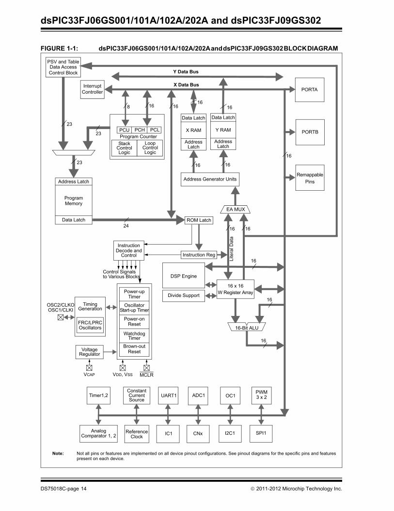
Figure 1-1 shows a general block diagram of the coreand peripheral modules in the devices. Table 1-1 lists thefunctions of the various pins shown in the pinoutdiagrams.
Note: This data sheet summarizes the features ofthe dsPIC33FJ06GS001/101A/102A/202Aand dsPIC33FJ09GS302 families ofdevices. It is not intended to be acomprehensive reference source. Tocomplement the information in this datasheet, refer to the “dsPIC33F/PIC24HFamily Reference Manual”. Please see theMicrochip web site (www.microchip.com)for the latest “dsPIC33F/PIC24H FamilyReference Manual” sections.
2011-2012 Microchip Technology Inc. DS75018C-page 13
dsPIC33FJ06GS001/101A/102A/202A and dsPIC33FJ09GS302
FIGURE 1-1: dsPIC33FJ06GS001/101A/102A/202A and dsPIC33FJ09GS302 BLOCK DIAGRAM
16
OSC1/CLKIOSC2/CLKO
VDD, VSS
TimingGeneration
MCLR
Power-upTimer
OscillatorStart-up Timer
Power-onReset
WatchdogTimer
Brown-outReset
FRC/LPRCOscillators
RegulatorVoltage
VCAP
IC1 I2C1
PORTA
InstructionDecode and
Control
PCH PCL
16
Program Counter
16-Bit ALU
23
23
24
23
Instruction Reg
PCU
16 x 16W Register Array
ROM Latch
16
EA MUX
16
16
8
InterruptController
PSV and TableData AccessControl Block
StackControlLogic
LoopControlLogic
Data Latch
AddressLatch
Address Latch
Program
Data Latch
L
itera
l Da
ta 16 16
16
16
Data Latch
AddressLatch
16
X RAM Y RAM
16
Y Data Bus
X Data Bus
DSP Engine
Divide Support
16
Control Signals to Various Blocks
ADC1Timer1,2
PORTB
Address Generator Units
CNx
UART1PWM3 x 2
Remappable
Pins
SPI1
OC1
AnalogComparator 1, 2
Note: Not all pins or features are implemented on all device pinout configurations. See pinout diagrams for the specific pins and featurespresent on each device.
Reference
ConstantCurrentSource
Clock
Memory
DS75018C-page 14 2011-2012 Microchip Technology Inc.

dsPIC33FJ06GS001/101A/102A/202A and dsPIC33FJ09GS302
TABLE 1-1: PINOUT I/O DESCRIPTIONS
Pin NamePin
TypeBufferType
PPS Capable
Description
AN0-AN7 I Analog No Analog input channels.
CLKI
CLKO
I
O
ST/CMOS
—
No
No
External clock source input. Always associated with OSC1 pin function.Oscillator crystal output. Connects to crystal or resonator in Crystal Oscillator mode. Optionally functions as CLKO in RC and EC modes. Always associated with OSC2 pin function.
OSC1
OSC2
I
I/O
ST/CMOS
—
No
No
Oscillator crystal input. ST buffer when configured in RC mode; CMOS otherwise.Oscillator crystal output. Connects to crystal or resonator in Crystal Oscillator mode. Optionally functions as CLKO in RC and EC modes.
CN0-CN15 I ST No Change notification inputs. Can be software programmed for internal weak pull-ups on all inputs.
IC1 I ST Yes Capture Input 1.
OCFAOC1
IO
ST—
YesYes
Compare Fault A input (for Compare Channel 1).Compare Output 1.
INT0INT1INT2
III
STSTST
NoYesYes
External Interrupt 0.External Interrupt 1.External Interrupt 2.
RA0-RA4 I/O ST No PORTA is a bidirectional I/O port.
RB0-RB15(1) I/O ST No PORTB is a bidirectional I/O port.
RP0-RP15(1) I/O ST No Remappable I/O pins.
T1CKT2CK
II
STST
YesYes
Timer1 external clock input.Timer2 external clock input.
U1CTSU1RTSU1RXU1TX
IOIO
ST—ST—
YesYesYesYes
UART1 Clear-to-Send.UART1 Ready-to-Send.UART1 receive.UART1 transmit.
SCK1SDI1SDO1SS1
I/OIO
I/O
STST—ST
YesYesYesYes
Synchronous serial clock input/output for SPI1.SPI1 data in.SPI1 data out.SPI1 slave synchronization or frame pulse I/O.
SCL1SDA1
I/OI/O
STST
NoNo
Synchronous serial clock input/output for I2C1.Synchronous serial data input/output for I2C1.
TMSTCKTDITDO
IIIO
TTLTTLTTL—
NoNoNoNo
JTAG Test mode select pin.JTAG test clock input pin.JTAG test data input pin.JTAG test data output pin.
Legend: CMOS = CMOS compatible input or output Analog = Analog input I = InputST = Schmitt Trigger input with CMOS levels P = Power O = OutputTTL = Transistor-Transistor Logic PPS = Peripheral Pin Select — = Does not apply
Note 1: Not all pins are available on all devices. Refer to the specific device in the “Pin Diagrams” section for availability.
2: This pin is available on dsPIC33FJ09GS302 devices only.
2011-2012 Microchip Technology Inc. DS75018C-page 15

dsPIC33FJ06GS001/101A/102A/202A and dsPIC33FJ09GS302
CMP1ACMP1BCMP1CCMP1DCMP2ACMP2BCMP2CCMP2D
IIIIIIII
AnalogAnalogAnalogAnalogAnalogAnalogAnalogAnalog
NoNoNoNoNoNoNoNo
Comparator 1 Channel A.Comparator 1 Channel B.Comparator 1 Channel C.Comparator 1 Channel D.Comparator 2 Channel A.Comparator 2 Channel B.Comparator 2 Channel C.Comparator 2 Channel D.
DACOUT O — No DAC output voltage.
ACMP1-ACMP2 O — Yes DAC trigger to PWM module.
ISRC1(2)
ISRC2(2)
ISRC3(2)
ISRC4(2)
OOOO
————
NoNoNoNo
Constant Current Source Output 1.Constant Current Source Output 2.Constant Current Source Output 3.Constant Current Source Output 4.
EXTREF I Analog No External voltage reference input for the reference DACs.
REFCLKO O — Yes REFCLKO output signal is a postscaled derivative of the system clock.
FLT1-FLT8 I ST Yes Fault inputs to PWM module.
SYNCI1-SYNCI2SYNCO1PWM1LPWM1HPWM2LPWM2HPWM4LPWM4H
IOOOOOOO
ST———————
YesYesNoNoNoNoYesYes
External synchronization signal to PWM master time base.PWM master time base for external device synchronization.PWM1 low output.PWM1 high output.PWM2 low output.PWM2 high output.PWM4 low output.PWM4 high output.
PGED1PGEC1
PGED2PGEC2
PGED3(1)
PGEC3(1)
I/OI
I/OI
I/OI
STST
STST
STST
NoNo
NoNo
NoNo
Data I/O pin for programming/debugging Communication Channel 1.Clock input pin for programming/debugging Communication Channel 1.Data I/O pin for programming/debugging Communication Channel 2.Clock input pin for programming/debugging Communication Channel 2.Data I/O pin for programming/debugging Communication Channel 3.Clock input pin for programming/debugging Communication Channel 3.
MCLR I/P ST No Master Clear (Reset) input. This pin is an active-low Reset to the device.
AVDD P P No Positive supply for analog modules. This pin must be connected at all times. AVDD is connected to VDD on 18 and 28-pin devices.
AVSS P P No Ground reference for analog modules. AVSS is connected to VSS on 18 and 28-pin devices.
VDD P — No Positive supply for peripheral logic and I/O pins.
VCAP P — No CPU logic filter capacitor connection.
VSS P — No Ground reference for logic and I/O pins.
TABLE 1-1: PINOUT I/O DESCRIPTIONS (CONTINUED)
Pin NamePin
TypeBufferType
PPS Capable
Description
Legend: CMOS = CMOS compatible input or output Analog = Analog input I = InputST = Schmitt Trigger input with CMOS levels P = Power O = OutputTTL = Transistor-Transistor Logic PPS = Peripheral Pin Select — = Does not apply
Note 1: Not all pins are available on all devices. Refer to the specific device in the “Pin Diagrams” section for availability.
2: This pin is available on dsPIC33FJ09GS302 devices only.
DS75018C-page 16 2011-2012 Microchip Technology Inc.

dsPIC33FJ06GS001/101A/102A/202A and dsPIC33FJ09GS302
2.0 GUIDELINES FOR GETTING STARTED WITH 16-BIT DIGITAL SIGNAL CONTROLLERS
2.1 Basic Connection Requirements
Getting started with the dsPIC33FJ06GS001/101A/102A/202A and dsPIC33FJ09GS302 family of 16-bitDigital Signal Controllers (DSCs) requires attention to aminimal set of device pin connections beforeproceeding with development. The following is a list ofpin names which must always be connected:
• All VDD and VSS pins (see Section 2.2 “Decoupling Capacitors”)
• All AVDD and AVSS pins, regardless if ADC module is not used (see Section 2.2 “Decoupling Capacitors”)
• VCAP (see Section 2.3 “Capacitor on Internal Voltage Regulator (VCAP)”)
• MCLR pin (see Section 2.4 “Master Clear (MCLR) Pin”)
• PGECx/PGEDx pins used for In-Circuit Serial Programming™ (ICSP™) and debugging purposes (see Section 2.5 “ICSP™ Pins”)
• OSC1 and OSC2 pins when external oscillator source is used (see Section 2.6 “External Oscillator Pins”)
2.2 Decoupling Capacitors
The use of decoupling capacitors on every pair ofpower supply pins, such as VDD, VSS, AVDD andAVSS, is required.
Consider the following criteria when using decouplingcapacitors:
• Value and type of capacitor: Recommendation of 0.1 µF (100 nF), 10-20V. This capacitor should be a low-ESR and have resonance frequency in the range of 20 MHz and higher. It is recommended that ceramic capacitors be used.
• Placement on the printed circuit board: The decoupling capacitors should be placed as close to the pins as possible. It is recommended to place the capacitors on the same side of the board as the device. If space is constricted, the capacitor can be placed on another layer on the PCB using a via; however, ensure that the trace length from the pin to the capacitor is within one-quarter inch (6 mm) in length.
• Handling high-frequency noise: If the board is experiencing high-frequency noise, upward of tens of MHz, add a second ceramic type capacitor in parallel to the above described decoupling capacitor. The value of the second capacitor can be in the range of 0.01 µF to 0.001 µF. Place this second capacitor next to the primary decoupling capacitor. In high-speed circuit designs, consider implementing a decade pair of capacitances as close to the power and ground pins as possible; for example, 0.1 µF in parallel with 0.001 µF.
• Maximizing performance: On the board layout from the power supply circuit, run the power and return traces to the decoupling capacitors first, and then to the device pins. This ensures that the decoupling capacitors are first in the power chain. Equally important is to keep the trace length between the capacitor and the power pins to a minimum, thereby reducing PCB track inductance.
Note 1: This data sheet summarizes the featuresof the dsPIC33FJ06GS001/101A/102A/202A and dsPIC33FJ09GS302 family ofdevices. It is not intended to be acomprehensive reference source. Tocomplement the information in this datasheet, refer to the “dsPIC33F/PIC24HFamily Reference Manual”, which isavailable from the Microchip web site(www.microchip.com).
2: Some registers and associated bitsdescribed in this section may not beavailable on all devices. Refer toSection 4.0 “Memory Organization” inthis data sheet for device-specific registerand bit information.
2011-2012 Microchip Technology Inc. DS75018C-page 17

dsPIC33FJ06GS001/101A/102A/202A and dsPIC33FJ09GS302
FIGURE 2-1: RECOMMENDED MINIMUM CONNECTION
2.2.1 TANK CAPACITORS
On boards with power traces running longer thansix inches in length, it is suggested to use a tank capac-itor for integrated circuits including DSCs to supply alocal power source. The value of the tank capacitorshould be determined based on the trace resistancethat connects the power supply source to the device,and the maximum current drawn by the device in theapplication. In other words, select the tank capacitor sothat it meets the acceptable voltage sag at the device;typical values range from 4.7 µF to 47 µF.
2.3 Capacitor on Internal Voltage Regulator (VCAP)
A low-ESR (<0.5 Ohms) capacitor is required on theVCAP pin, which is used to stabilize the voltage regulatoroutput voltage. The VCAP pin must not be connected toVDD, and must have a capacitor between 4.7 µF and10 µF, 16V connected to ground. The type can beceramic or tantalum. Refer to Section 25.0 “ElectricalCharacteristics” for additional information.
The placement of this capacitor should be close to theVCAP. It is recommended that the trace length notexceed one-quarter inch (6 mm). Refer to Section 22.2“On-Chip Voltage Regulator” for details.
2.4 Master Clear (MCLR) Pin
The MCLR pin provides for two specific devicefunctions:
• Device Reset• Device Programming and Debugging
During device programming and debugging, theresistance and capacitance that can be added to thepin must be considered. Device programmers anddebuggers drive the MCLR pin. Consequently,specific voltage levels (VIH and VIL) and fast signaltransitions must not be adversely affected. Therefore,specific values of R and C will need to be adjustedbased on the application and PCB requirements.
For example, as shown in Figure 2-2, it is recommendedthat the capacitor, C, be isolated from the MCLR pinduring programming and debugging operations.
Place the components shown in Figure 2-2 withinone-quarter inch (6 mm) from the MCLR pin.
FIGURE 2-2: EXAMPLE OF MCLR PIN CONNECTIONS
dsPIC33FV
DD
VS
S
VDD
VSS
VSS
VDD
AV
DD
AV
SS
VD
D
VS
S
0.1 µFCeramic
0.1 µFCeramic
0.1 µFCeramic
0.1 µFCeramic
C
R
VDD
MCLR
0.1 µFCeramic
VC
AP
L1(1)
R1
10 µFTantalum
Note 1: As an option, instead of a hard-wired connection, aninductor (L1) can be substituted between VDD andAVDD to improve ADC noise rejection. The inductorimpedance should be less than 1 and the inductorcapacity greater than 10 mA.
Where:
f FCNV
2--------------=
f 1
2 LC -----------------------=
L1
2f C ---------------------- 2
=
(i.e., ADC conversion rate/2)
Note 1: R 10 k is recommended. A suggested starting value is 10 k. Ensure that the MCLR pin VIH and VIL specifications are met.
2: R1 470 will limit any current flowing into MCLR from the external capacitor, C, in the event of MCLR pin breakdown due to Electrostatic Discharge (ESD) or Electrical Overstress (EOS). Ensure that the MCLR pin VIH and VIL specifications are met.
C
R1(2)R(1)
VDD
MCLR
dsPIC33FJP
DS75018C-page 18 2011-2012 Microchip Technology Inc.

dsPIC33FJ06GS001/101A/102A/202A and dsPIC33FJ09GS302
2.5 ICSP™ Pins
The PGECx and PGEDx pins are used for In-CircuitSerial Programming™ (ICSP™) and debuggingpurposes. It is recommended to keep the trace lengthbetween the ICSP connector and the ICSP pins on thedevice as short as possible. If the ICSP connector isexpected to experience an ESD event, a series resistoris recommended, with the value in the range of a fewtens of Ohms, not to exceed 100 Ohms.
Pull-up resistors, series diodes, and capacitors on thePGECx and PGEDx pins, are not recommended as theywill interfere with the programmer/debugger communi-cations to the device. If such discrete components arean application requirement, they should be removedfrom the circuit during programming and debugging.Alternatively, refer to the AC/DC characteristics and tim-ing requirements information in the respective deviceFlash programming specification for information oncapacitive loading limits, and Input Voltage High (VIH)and Input Voltage Low (VIL) pin requirements.
Ensure that the “Communication Channel Select”(i.e., PGECx/PGEDx pins), programmed into thedevice matches the physical connections for the ICSPto MPLAB® ICD 3 or MPLAB REAL ICE™.
For more information on MPLAB ICD 3 and REAL ICEconnection requirements, refer to the followingdocuments that are available on the Microchip web site(www.microchip.com):
• “Using MPLAB® ICD 3” (poster) (DS51765)
• “Multi-Tool Design Advisory” (DS51764)
• “MPLAB® REAL ICE™ In-Circuit Emulator User’s Guide” (DS51616)
• “Using MPLAB® REAL ICE™” (poster) (DS51749)
2.6 External Oscillator Pins
Many DSCs have options for at least two oscillators: ahigh-frequency primary oscillator and a low-frequencysecondary oscillator (refer to Section 8.0 “OscillatorConfiguration” for details).
The oscillator circuit should be placed on the sameside of the board as the device. Also, place theoscillator circuit close to the respective oscillator pins,not exceeding one-half inch (12 mm) distancebetween them. The load capacitors should be placednext to the oscillator itself, on the same side of theboard. Use a grounded copper pour around theoscillator circuit to isolate them from surroundingcircuits. The grounded copper pour should be routeddirectly to the MCU ground. Do not run any signaltraces or power traces inside the ground pour. Also, ifusing a two-sided board, avoid any traces on theother side of the board where the crystal is placed. Asuggested layout is shown in Figure 2-3.
FIGURE 2-3: SUGGESTED PLACEMENT OF THE OSCILLATOR CIRCUIT
13
Main Oscillator
Guard Ring
Guard Trace
SecondaryOscillator
14
15
16
17
18
19
20
2011-2012 Microchip Technology Inc. DS75018C-page 19

dsPIC33FJ06GS001/101A/102A/202A and dsPIC33FJ09GS302
2.7 Oscillator Value Conditions on Device Start-up
If the PLL of the target device is enabled andconfigured for the device start-up oscillator, themaximum oscillator source frequency must be limitedto 4 MHz < FIN < 8 MHz to comply with device PLLstart-up conditions. This means that if the externaloscillator frequency is outside of this range, theapplication must start up in the FRC mode first. Thedefault PLL settings after a POR, with an oscillatorfrequency outside of this range, will violate the deviceoperating speed.
Once the device powers up, the application firmwarecan initialize the PLL SFRs, CLKDIV and PLLDBF to asuitable value, and then perform a clock switch to theOscillator + PLL clock source. Note that clock switchingmust be enabled in the device Configuration Word.
2.8 Configuration of Analog and Digital Pins During ICSP Operations
If MPLAB ICD 3 or REAL ICE is selected as a debug-ger, it automatically initializes all of the Analog-to-Digitalinput pins (ANx) as “digital” pins, by setting all bits in theADPCFG register.
The bits in the registers that correspond to theAnalog-to-Digital pins that are initialized by MPLABICD 3 or REAL ICE, must not be cleared by the userapplication firmware; otherwise, communication errorswill result between the debugger and the device.
If your application needs to use certain Analog-to-Digitalpins as analog input pins during the debug session, theuser application must clear the corresponding bits inthe ADPCFG register during initialization of the ADCmodule.
When MPLAB ICD 3 or REAL ICE is used as aprogrammer, the user application firmware mustcorrectly configure the ADPCFG register. Automaticinitialization of these registers is only done duringdebugger operation. Failure to correctly configure theregister(s) will result in all Analog-to-Digital pins beingrecognized as analog input pins, resulting in the portvalue being read as a logic ‘0’, which may affect userapplication functionality.
2.9 Unused I/Os
Unused I/O pins should be configured as outputs anddriven to a logic low state.
Alternatively, connect a 1k to 10k resistor between VSS
and unused pins, and drive the output to logic low.
2.10 Typical Application Connection Examples
Examples of typical application connections are shownin Figure 2-4 through Figure 2-8.
DS75018C-page 20 2011-2012 Microchip Technology Inc.

dsPIC33FJ06GS001/101A/102A/202A and dsPIC33FJ09GS302
FIGURE 2-4: DIGITAL PFC
FIGURE 2-5: BOOST CONVERTER IMPLEMENTATION
VAC
IPFC
VHV_BUS
ADC Channel ADC Channel ADC ChannelPWM Output
|VAC|
k1
k2
k3
FET
dsPIC33FJ06GS001
Driver
IPFC
VOUTPUT
ADC Channel ADC ADC ChannelPWM
k1
k2
k3
FET
dsPIC33FJ06GS001
VINPUT
Channel Output
Driver
2011-2012 Microchip Technology Inc. DS75018C-page 21

dsPIC33FJ06GS001/101A/102A/202A and dsPIC33FJ09GS302
FIGURE 2-6: SINGLE-PHASE SYNCHRONOUS BUCK CONVERTER
FIGURE 2-7: INTERLEAVED PFC
k1
AnalogComp.
k2k7
PW
M
PW
M ADCChannel
ADCChannel
5V Output
I5V
12V Input
dsPIC33FJ06GS202A
FETDriver
VAC
VOUT+
ADC Channel PWM ADCPWM
|VAC|
k4 k3
FET
dsPIC33FJ06GS202A
Driver
VOUT-
ADC Channel
FETDriver
ADC
k1 k2
Channel ChannelADC
Channel
DS75018C-page 22 2011-2012 Microchip Technology Inc.

dsPIC33FJ06GS001/101A/102A/202A and dsPIC33FJ09GS302
FIGURE 2-8: PHASE-SHIFTED FULL-BRIDGE CONVERTER
VIN+
VIN-
S1
Gate 4
Gate 2
Gate 3Gate 1
AnalogGround
VOUT+
VOUT-
k2FET
Driver
k1
FETDriver
FET Driver
Gate 1
Gate 2
S1 Gate 3
Gate 4
S3
S3
Gate 6
Gate 5
Gat
e 6Gate 5
dsPIC33FJ09GS302
PWM
PWM ADCChannel
PWM ADCChannel
2011-2012 Microchip Technology Inc. DS75018C-page 23

dsPIC33FJ06GS001/101A/102A/202A and dsPIC33FJ09GS302
NOTES:
DS75018C-page 24 2011-2012 Microchip Technology Inc.

dsPIC33FJ06GS001/101A/102A/202A and dsPIC33FJ09GS302
3.0 CPU
The CPU module has a 16-bit (data) modified Harvardarchitecture with an enhanced instruction set, includingsignificant support for DSP. The CPU has a 24-bitinstruction word with a variable length opcode field. TheProgram Counter (PC) is 23 bits wide and addresses upto 4M x 24 bits of user program memory space. Theactual amount of program memory implemented variesfrom device to device. A single-cycle instruction prefetchmechanism is used to help maintain throughput andprovides predictable execution. All instructions execute ina single cycle, with the exception of instructions thatchange the program flow, the double-word move (MOV.D)instruction and the table instructions. Overhead-freeprogram loop constructs are supported using the DO andREPEAT instructions, both of which are interruptible atany point.
The dsPIC33FJ06GS001/101A/102A/202A anddsPIC33FJ09GS302 devices have sixteen, 16-bitworking registers in the programmer’s model. Each of theworking registers can serve as a Data, Address orAddress Offset register. The sixteenth working register(W15) operates as a software Stack Pointer (SP) forinterrupts and calls.
There are two classes of instruction: MCU and DSP.These two instruction classes are seamlesslyintegrated into a single CPU. The instruction setincludes many addressing modes and is designedfor optimum C compiler efficiency. For most instruc-tions, the devices are capable of executing a data(or program data) memory read, a working register(data) read, a data memory write and a program(instruction) memory read per instruction cycle. As aresult, three parameter instructions can be sup-ported, allowing A + B = C operations to be executedin a single cycle.
A block diagram of the CPU is shown in Figure 3-1,and the programmer’s model is shown in Figure 3-2.
3.1 Data Addressing Overview
The data space can be addressed as 32K words or64 Kbytes and is split into two blocks, referred to as Xand Y data memory. Each memory block has its ownindependent Address Generation Unit (AGU). TheMCU class of instructions operates solely throughthe X memory AGU, which accesses the entirememory map as one linear data space. Certain DSPinstructions operate through the X and Y AGUs tosupport dual operand reads, which splits the dataaddress space into two parts. The X and Y data spaceboundary is device-specific.
Overhead-free circular buffers (Modulo Addressingmode) are supported in both X and Y address spaces.The Modulo Addressing removes the software boundarychecking overhead for DSP algorithms. Furthermore,the X AGU Circular Addressing can be used with any ofthe MCU class of instructions. The X AGU also supportsBit-Reversed Addressing to greatly simplify input oroutput data reordering for radix-2 FFT algorithms.
The upper 32 Kbytes of the data space memory mapcan optionally be mapped into program space at any16K program word boundary defined by the 8-bitProgram Space Visibility Page (PSVPAG) register. Theprogram-to-data space mapping feature lets anyinstruction access program space as if it were dataspace.
3.2 DSP Engine Overview
The DSP engine features a high-speed, 17-bit by 17-bitmultiplier, a 40-bit ALU, two 40-bit saturatingaccumulators and a 40-bit bidirectional barrel shifter.The barrel shifter is capable of shifting a 40-bit value upto 16 bits, right or left, in a single cycle. The DSPinstructions operate seamlessly with all otherinstructions and have been designed for optimal real-time performance. The MAC instruction and other asso-ciated instructions can concurrently fetch two dataoperands from memory while multiplying two Wregisters and accumulating and optionally saturatingthe result in the same cycle. This instructionfunctionality requires that the RAM data space be splitfor these instructions and linear for all others. Dataspace partitioning is achieved in a transparent andflexible manner through dedicating certain workingregisters to each address space.
Note 1: This data sheet summarizes the featuresof the dsPIC33FJ06GS001/101A/102A/202A and dsPIC33FJ09GS302 familiesof devices. It is not intended to be acomprehensive reference source. Tocomplement the information in this datasheet, refer to Section 2. “CPU”(DS70204) in the “dsPIC33F/PIC24HFamily Reference Manual”, which isavailable from the Microchip web site(www.microchip.com).
2: Some registers and associated bitsdescribed in this section may not beavailable on all devices. Refer toSection 4.0 “Memory Organization” inthis data sheet for device-specific registerand bit information.
2011-2012 Microchip Technology Inc. DS75018C-page 25

dsPIC33FJ06GS001/101A/102A/202A and dsPIC33FJ09GS302
3.3 Special MCU Features
A 17-bit by 17-bit single-cycle multiplier is shared by boththe MCU ALU and DSP engine. The multiplier can per-form signed, unsigned and mixed-sign multiplication.Using a 17-bit by 17-bit multiplier for 16-bit by 16-bitmultiplication not only allows you to perform mixed-signmultiplication, it also achieves accurate results for specialoperations, such as (-1.0) x (-1.0).
The 16/16 and 32/16 divide operations are supported,both fractional and integer. All divide instructions areiterative operations. They must be executed within aREPEAT loop, resulting in a total execution time of19 instruction cycles. The divide operation can beinterrupted during any of those 19 cycles without loss ofdata.
A 40-bit barrel shifter is used to perform up to a 16-bitleft or right shift in a single cycle. The barrel shifter canbe used by both MCU and DSP instructions.
FIGURE 3-1: CPU CORE BLOCK DIAGRAM
InstructionDecode and
Control
PCH PCLProgram Counter
16-Bit ALU
24
23
Instruction Reg
PCU
ROM Latch
EA MUX
InterruptController
StackControlLogic
LoopControlLogic
Data Latch
AddressLatch
Control Signalsto Various Blocks
Lite
ral D
ata
16 16
16
To Peripheral Modules
Data Latch
AddressLatch
16
X RAM Y RAM
Address Generator Units
16
Y Data Bus
X Data Bus
DSP Engine
Divide Support
16
16
23
23
168
PSV and TableData AccessControl Block
16
16
16
16
Program Memory
Data Latch
Address Latch
16 x 16W Register Array
DS75018C-page 26 2011-2012 Microchip Technology Inc.

dsPIC33FJ06GS001/101A/102A/202A and dsPIC33FJ09GS302
FIGURE 3-2: PROGRAMMER’S MODEL
PC22 PC0
7 0
D0D15
Program Counter
Data Table Page Address
STATUS Register
Working Registers
DSP OperandRegisters
W1
W2
W3
W4
W5
W6
W7
W8
W9
W10
W11
W12/DSP Offset
W13/DSP Write Back
W14/Frame Pointer
W15/Stack Pointer
DSP AddressRegisters
AD39 AD0AD31
DSPAccumulators
ACCA
ACCB
7 0
Program Space Visibility Page Address
Z
0
OA OB SA SB
RCOUNT15 0
REPEAT Loop Counter
DCOUNT15 0
DO Loop Counter
DOSTART
22 0
DO Loop Start Address
IPL2 IPL1
SPLIM Stack Pointer Limit Register
AD15
SRL
PUSH.S Shadow
DO Shadow
OAB SAB
15 0Core Configuration Register
Legend
CORCON
DA DC RA N
TBLPAG
PSVPAG
IPL0 OV
W0/WREG
SRH
DO Loop End AddressDOEND
22
C
2011-2012 Microchip Technology Inc. DS75018C-page 27

dsPIC33FJ06GS001/101A/102A/202A and dsPIC33FJ09GS302
3.4 CPU Control Registers
REGISTER 3-1: SR: CPU STATUS REGISTER
R-0 R-0 R/C-0 R/C-0 R-0 R/C-0 R -0 R/W-0
OA OB SA(1) SB(1) OAB SAB(1,4) DA DC
bit 15 bit 8
R/W-0(3) R/W-0(3) R/W-0(3) R-0 R/W-0 R/W-0 R/W-0 R/W-0
IPL<2:0>(2) RA N OV Z C
bit 7 bit 0
Legend:
C = Clearable bit R = Readable bit U = Unimplemented bit, read as ‘0’
S = Settable bit W = Writable bit -n = Value at POR
‘1’ = Bit is set ‘0’ = Bit is cleared x = Bit is unknown
bit 15 OA: Accumulator A Overflow Status bit
1 = Accumulator A overflowed0 = Accumulator A has not overflowed
bit 14 OB: Accumulator B Overflow Status bit
1 = Accumulator B overflowed0 = Accumulator B has not overflowed
bit 13 SA: Accumulator A Saturation ‘Sticky’ Status bit(1)
1 = Accumulator A is saturated or has been saturated at some time0 = Accumulator A is not saturated
bit 12 SB: Accumulator B Saturation ‘Sticky’ Status bit(1)
1 = Accumulator B is saturated or has been saturated at some time0 = Accumulator B is not saturated
bit 11 OAB: OA || OB Combined Accumulator Overflow Status bit
1 = Accumulators A or B have overflowed0 = Neither Accumulators A or B have overflowed
bit 10 SAB: SA || SB Combined Accumulator ‘Sticky’ Status bit(1,4)
1 = Accumulators A or B are saturated or have been saturated at some time in the past0 = Neither Accumulator A or B are saturated
bit 9 DA: DO Loop Active bit
1 = DO loop in progress0 = DO loop not in progress
bit 8 DC: MCU ALU Half Carry/Borrow bit
1 = A carry-out from the 4th low-order bit (for byte-sized data) or 8th low-order bit (for word-sized data)of the result occurred
0 = No carry-out from the 4th low-order bit (for byte-sized data) or 8th low-order bit (for word-sizeddata) of the result occurred
Note 1: This bit can be read or cleared (not set).
2: The IPL<2:0> bits are concatenated with the IPL3 bit (CORCON<3>) to form the CPU Interrupt Priority Level (IPL). The value in parentheses indicates the IPL if IPL3 = 1. User interrupts are disabled when IPL3 = 1.
3: The IPL<2:0> Status bits are read-only when NSTDIS = 1 (INTCON1<15>).
4: Clearing this bit will clear SA and SB.
DS75018C-page 28 2011-2012 Microchip Technology Inc.

dsPIC33FJ06GS001/101A/102A/202A and dsPIC33FJ09GS302
bit 7-5 IPL<2:0>: CPU Interrupt Priority Level Status bits(2,3)
111 = CPU Interrupt Priority Level is 7 (15), user interrupts disabled110 = CPU Interrupt Priority Level is 6 (14)101 = CPU Interrupt Priority Level is 5 (13)100 = CPU Interrupt Priority Level is 4 (12)011 = CPU Interrupt Priority Level is 3 (11)010 = CPU Interrupt Priority Level is 2 (10)001 = CPU Interrupt Priority Level is 1 (9)000 = CPU Interrupt Priority Level is 0 (8)
bit 4 RA: REPEAT Loop Active bit
1 = REPEAT loop in progress0 = REPEAT loop not in progress
bit 3 N: MCU ALU Negative bit
1 = Result was negative0 = Result was non-negative (zero or positive)
bit 2 OV: MCU ALU Overflow bit
This bit is used for signed arithmetic (2’s complement). It indicates an overflow of a magnitude thatcauses the sign bit to change state. 1 = Overflow occurred for signed arithmetic (in this arithmetic operation)0 = No overflow occurred
bit 1 Z: MCU ALU Zero bit
1 = An operation that affects the Z bit has set it at some time in the past0 = The most recent operation that affects the Z bit has cleared it (i.e., a non-zero result)
bit 0 C: MCU ALU Carry/Borrow bit
1 = A carry-out from the Most Significant bit of the result occurred0 = No carry-out from the Most Significant bit of the result occurred
REGISTER 3-1: SR: CPU STATUS REGISTER (CONTINUED)
Note 1: This bit can be read or cleared (not set).
2: The IPL<2:0> bits are concatenated with the IPL3 bit (CORCON<3>) to form the CPU Interrupt Priority Level (IPL). The value in parentheses indicates the IPL if IPL3 = 1. User interrupts are disabled when IPL3 = 1.
3: The IPL<2:0> Status bits are read-only when NSTDIS = 1 (INTCON1<15>).
4: Clearing this bit will clear SA and SB.
2011-2012 Microchip Technology Inc. DS75018C-page 29

dsPIC33FJ06GS001/101A/102A/202A and dsPIC33FJ09GS302
REGISTER 3-2: CORCON: CORE CONTROL REGISTER
U-0 U-0 U-0 R/W-0 R/W-0 R-0 R-0 R-0
— — — US EDT(1) DL<2:0>
bit 15 bit 8
R/W-0 R/W-0 R/W-1 R/W-0 R/C-0 R/W-0 R/W-0 R/W-0
SATA SATB SATDW ACCSAT IPL3(2) PSV RND IF
bit 7 bit 0
Legend: C = Clearable bit
R = Readable bit W = Writable bit -n = Value at POR ‘1’ = Bit is set
0’ = Bit is cleared ‘x = Bit is unknown U = Unimplemented bit, read as ‘0’
bit 15-13 Unimplemented: Read as ‘0’
bit 12 US: DSP Multiply Unsigned/Signed Control bit
1 = DSP engine multiplies are unsigned 0 = DSP engine multiplies are signed
bit 11 EDT: Early DO Loop Termination Control bit(1)
1 = Terminate executing DO loop at end of current loop iteration0 = No effect
bit 10-8 DL<2:0>: DO Loop Nesting Level Status bits
111 = 7 DO loops active•••001 = 1 DO loop active000 = 0 DO loops active
bit 7 SATA: ACCA Saturation Enable bit
1 = Accumulator A saturation is enabled0 = Accumulator A saturation is disabled
bit 6 SATB: ACCB Saturation Enable bit
1 = Accumulator B saturation is enabled0 = Accumulator B saturation is disabled
bit 5 SATDW: Data Space Write from DSP Engine Saturation Enable bit
1 = Data space write saturation is enabled0 = Data space write saturation is disabled
bit 4 ACCSAT: Accumulator Saturation Mode Select bit
1 = 9.31 saturation (super saturation)0 = 1.31 saturation (normal saturation)
bit 3 IPL3: CPU Interrupt Priority Level Status bit 3(2)
1 = CPU Interrupt Priority Level is greater than 70 = CPU Interrupt Priority Level is 7 or less
bit 2 PSV: Program Space Visibility in Data Space Enable bit
1 = Program space is visible in data space0 = Program space is not visible in data space
bit 1 RND: Rounding Mode Select bit
1 = Biased (conventional) rounding is enabled0 = Unbiased (convergent) rounding is enabled
bit 0 IF: Integer or Fractional Multiplier Mode Select bit
1 = Integer mode enabled for DSP multiply ops0 = Fractional mode enabled for DSP multiply ops
Note 1: This bit will always read as ‘0’.
2: The IPL3 bit is concatenated with the IPL<2:0> bits (SR<7:5>) to form the CPU Interrupt Priority Level.
DS75018C-page 30 2011-2012 Microchip Technology Inc.

dsPIC33FJ06GS001/101A/102A/202A and dsPIC33FJ09GS302
3.5 Arithmetic Logic Unit (ALU)
The ALU is 16 bits wide and is capable of addition,subtraction, bit shifts and logic operations. Unlessotherwise mentioned, arithmetic operations are 2’scomplement in nature. Depending on the operation, theALU can affect the values of the Carry (C), Zero (Z),Negative (N), Overflow (OV) and Digit Carry (DC) Statusbits in the SR register. The C and DC Status bits operateas Borrow and Digit Borrow bits, respectively, forsubtraction operations.
The ALU can perform 8-bit or 16-bit operations,depending on the mode of the instruction that is used.Data for the ALU operation can come from the Wregister array or data memory, depending on theaddressing mode of the instruction. Likewise, outputdata from the ALU can be written to the W register arrayor a data memory location.
Refer to the “16-Bit MCU and DSC Programmer’sReference Manual” (DS70157) for information on theSR bits affected by each instruction.
The CPU incorporates hardware support for both multipli-cation and division. This includes a dedicated hardwaremultiplier and support hardware for 16-bit divisor division.
3.5.1 MULTIPLIER
Using the high-speed, 17-bit x 17-bit multiplier of theDSP engine, the ALU supports unsigned, signed ormixed-sign operation in several MCU multiplicationmodes:
• 16-bit x 16-bit signed
• 16-bit x 16-bit unsigned
• 16-bit signed x 5-bit (literal) unsigned
• 16-bit unsigned x 16-bit unsigned
• 16-bit unsigned x 5-bit (literal) unsigned
• 16-bit unsigned x 16-bit signed
• 8-bit unsigned x 8-bit unsigned
3.5.2 DIVIDER
The divide block supports 32-bit/16-bit and 16-bit/16-bitsigned and unsigned integer divide operations with thefollowing data sizes:
• 32-bit signed/16-bit signed divide
• 32-bit unsigned/16-bit unsigned divide
• 16-bit signed/16-bit signed divide
• 16-bit unsigned/16-bit unsigned divide
The quotient for all divide instructions ends up in W0 andthe remainder in W1. 16-bit signed and unsigned DIVinstructions can specify any W register for both the 16-bitdivisor (Wn) and any W register (aligned) pair(W(m + 1):Wm) for the 32-bit dividend. The dividealgorithm takes one cycle per bit of divisor, so both 32-bit/16-bit and 16-bit/16-bit instructions take the samenumber of cycles to execute.
3.6 DSP Engine
The DSP engine consists of a high-speed, 17-bit x 17-bitmultiplier, a barrel shifter and a 40-bit adder/subtracter(with two target accumulators, round and saturationlogic).
The dsPIC33FJ06GS001/101A/102A/202A anddsPIC33FJ09GS302 devices feature a single-cycleinstruction flow architecture; therefore, concurrentoperation of the DSP engine with MCU instruction flow isnot possible. However, some MCU ALU and DSP engineresources can be used concurrently by the sameinstruction (for example, ED, EDAC).
The DSP engine can also perform inherentaccumulator-to-accumulator operations that require noadditional data. These instructions are ADD, SUB andNEG.
The DSP engine has options selected through bits inthe CPU Core Control register (CORCON), as listedbelow:
• Fractional or Integer DSP Multiply (IF)
• Signed or Unsigned DSP Multiply (US)
• Conventional or Convergent Rounding (RND)
• Automatic Saturation On/Off for ACCA (SATA)
• Automatic Saturation On/Off for ACCB (SATB)
• Automatic Saturation On/Off for Writes to Data Memory (SATDW)
• Accumulator Saturation mode Selection (ACCSAT)
A block diagram of the DSP engine is shown inFigure 3-3.
TABLE 3-1: DSP INSTRUCTIONS SUMMARY
InstructionAlgebraic Operation
ACC Write Back
CLR A = 0 Yes
ED A = (x – y)2 No
EDAC A = A + (x – y)2 No
MAC A = A + (x * y) Yes
MAC A = A + x2 No
MOVSAC No change in A Yes
MPY A = x * y No
MPY A = x2 No
MPY.N A = – x * y No
MSC A = A – x * y Yes
2011-2012 Microchip Technology Inc. DS75018C-page 31

dsPIC33FJ06GS001/101A/102A/202A and dsPIC33FJ09GS302
FIGURE 3-3: DSP ENGINE BLOCK DIAGRAM
Zero Backfill
Sign-Extend
BarrelShifter
40-Bit Accumulator A
40-Bit Accumulator B RoundLogic
X D
ata
Bus
To/From W Array
Adder
Saturate
Negate
32
3233
16
16 16
16
40 40
4040
Saturate
Y D
ata
Bus
40
Carry/Borrow Out
Carry/Borrow In
16
40
Multiplier/Scaler17-Bit
DS75018C-page 32 2011-2012 Microchip Technology Inc.

dsPIC33FJ06GS001/101A/102A/202A and dsPIC33FJ09GS302
3.6.1 MULTIPLIER
The 17-bit x 17-bit multiplier is capable of signed orunsigned operation and can multiplex its output using ascaler to support either 1.31 fractional (Q31) or 32-bitinteger results. Unsigned operands are zero-extendedinto the 17th bit of the multiplier input value. Signedoperands are sign-extended into the 17th bit of themultiplier input value. The output of the 17-bit x 17-bitmultiplier/scaler is a 33-bit value that is sign-extendedto 40 bits. Integer data is inherently represented as asigned 2’s complement value, where the MostSignificant bit (MSb) is defined as a sign bit. The rangeof an N-bit 2’s complement integer is -2N-1 to 2N-1 – 1.
• For a 16-bit integer, the data range is -32768 (0x8000) to 32767 (0x7FFF) including 0
• For a 32-bit integer, the data range is -2,147,483,648 (0x8000 0000) to 2,147,483,647 (0x7FFF FFFF)
When the multiplier is configured for fractionalmultiplication, the data is represented as a 2’scomplement fraction, where the MSb is defined as asign bit and the radix point is implied to lie just after thesign bit (QX format). The range of an N-bit 2’scomplement fraction with this implied radix point is -1.0to (1 – 21-N). For a 16-bit fraction, the Q15 data rangeis -1.0 (0x8000) to 0.999969482 (0x7FFF) including 0and has a precision of 3.01518x10⁻⁵. In Fractionalmode, the 16 x 16 multiply operation generates a1.31 product that has a precision of 4.65661 x 10⁻¹⁰.
The same multiplier is used to support the MCUmultiply instructions, which include integer 16-bitsigned, unsigned and mixed-sign multiply operations.
The MUL instruction can be directed to use byte orword-sized operands. Byte operands will direct a 16-bitresult, and word operands will direct a 32-bit result tothe specified register(s) in the W array.
3.6.2 DATA ACCUMULATORS AND ADDER/SUBTRACTER
The data accumulator consists of a 40-bit adder/subtracter with automatic sign extension logic. It canselect one of two accumulators (A or B) as its pre-accumulation source and post-accumulation destination.For the ADD and LAC instructions, the data to be accumu-lated or loaded can be optionally scaled using the barrelshifter prior to accumulation.
3.6.2.1 Adder/Subtracter, Overflow and Saturation
The adder/subtracter is a 40-bit adder with an optionalzero input into one side, and either true or complementdata into the other input.
• In the case of addition, the Carry/Borrow input is active-high and the other input is true data (not complemented)
• In the case of subtraction, the Carry/Borrow input is active-low and the other input is complemented
The adder/subtracter generates Overflow Status bits,SA/SB and OA/OB, which are latched and reflected inthe STATUS register:
• Overflow from bit 39: This is a catastrophic overflow in which the sign of the accumulator is destroyed
• Overflow into guard bits, 32 through 39: This is a recoverable overflow. This bit is set whenever all the guard bits are not identical to each other.
The adder has an additional saturation block that controlsaccumulator data saturation, if selected. It uses the resultof the adder, the Overflow Status bits describedpreviously and the SAT<A:B> (CORCON<7:6>) andACCSAT (CORCON<4>) mode control bits to determinewhen and to what value to saturate.
Six STATUS register bits support saturation andoverflow:
• OA: ACCA overflowed into guard bits
• OB: ACCB overflowed into guard bits
• SA: ACCA saturated (bit 31 overflow and saturation)orACCA overflowed into guard bits and saturated (bit 39 overflow and saturation)
• SB: ACCB saturated (bit 31 overflow and saturation)orACCB overflowed into guard bits and saturated (bit 39 overflow and saturation)
• OAB: Logical OR of OA and OB
• SAB: Logical OR of SA and SB
The OA and OB bits are modified each time data passesthrough the adder/subtracter. When set, they indicatethat the most recent operation has overflowed into theaccumulator guard bits (bits 32 through 39). The OA andOB bits can also optionally generate an arithmetic warn-ing trap when set and the corresponding Overflow TrapEnable bits (OVATE, OVBTE) in the INTCON1 registerare set (refer to Section 7.0 “Interrupt Controller”).This allows the user application to take immediateaction, for example, to correct system gain.
The SA and SB bits are modified each time datapasses through the adder/subtracter, but can only becleared by the user application. When set, they indicatethat the accumulator has overflowed its maximumrange (bit 31 for 32-bit saturation or bit 39 for 40-bitsaturation) and will be saturated (if saturation isenabled). When saturation is not enabled, SA and SBdefault to bit 39 overflow and thus, indicate that a cata-strophic overflow has occurred. If the COVTE bit in theINTCON1 register is set, SA and SB bits will generatean arithmetic warning trap when saturation is disabled.
2011-2012 Microchip Technology Inc. DS75018C-page 33

dsPIC33FJ06GS001/101A/102A/202A and dsPIC33FJ09GS302
The Overflow and Saturation Status bits can optionally beviewed in the STATUS Register (SR) as the logical OR ofOA and OB (in bit OAB) and the logical OR of SA and SB(in bit SAB). Programmers can check one bit in theSTATUS Register to determine if either accumulator hasoverflowed, or one bit to determine if either accumulatorhas saturated. This is useful for complex numberarithmetic, which typically uses both accumulators.
The device supports three Saturation and Overflowmodes:
• Bit 39 Overflow and Saturation:When bit 39 overflow and saturation occurs, the saturation logic loads the maximally positive 9.31 (0x7FFFFFFFFF) or maximally negative 9.31 value (0x8000000000) into the target accumu-lator. The SA or SB bit is set and remains set until cleared by the user application. This condition is referred to as ‘super saturation’ and provides protection against erroneous data or unexpected algorithm problems (such as gain calculations).
• Bit 31 Overflow and Saturation:When bit 31 overflow and saturation occurs, the saturation logic then loads the maximally positive 1.31 value (0x007FFFFFFF) or maximally negative 1.31 value (0x0080000000) into the target accumu-lator. The SA or SB bit is set and remains set until cleared by the user application. When this Satura-tion mode is in effect, the guard bits are not used, so the OA, OB or OAB bits are never set.
• Bit 39 Catastrophic Overflow:Bit 39 Overflow Status bit, from the adder, is used to set the SA or SB bit, which remains set until cleared by the user application. No saturation operation is performed, and the accumulator is allowed to overflow, destroying its sign. If the COVTE bit in the INTCON1 register is set, a catastrophic overflow can initiate a trap exception.
3.6.3 ACCUMULATOR ‘WRITE BACK’
The MAC class of instructions (with the exception ofMPY, MPY.N, ED and EDAC) can optionally write arounded version of the high word (bits 31 through 16)of the accumulator that is not targeted by the instructioninto data space memory. The write is performed acrossthe X bus into combined X and Y address space. Thefollowing addressing modes are supported:
• W13, Register Direct:The rounded contents of the non-target accumulator are written into W13 as a 1.15 fraction.
• [W13] + = 2, Register Indirect with Post-Increment:The rounded contents of the non-target accumulator are written into the address pointed to by W13 as a 1.15 fraction. W13 is then incremented by 2 (for a word write).
3.6.3.1 Round Logic
The round logic is a combinational block that performsa conventional (biased) or convergent (unbiased)round function during an accumulator write (store). TheRound mode is determined by the state of the RND bitin the CORCON register. It generates a 16-bit,1.15 data value that is passed to the data space writesaturation logic. If rounding is not indicated by theinstruction, a truncated 1.15 data value is stored andthe least significant word is simply discarded.
Conventional rounding zero-extends bit 15 of the accu-mulator and adds it to the ACCxH word (bits 16 through31 of the accumulator).
• If the ACCxL word (bits 0 through 15 of the accumulator) is between 0x8000 and 0xFFFF (0x8000 included), ACCxH is incremented
• If ACCxL is between 0x0000 and 0x7FFF, ACCxH is left unchanged
A consequence of this algorithm is that over asuccession of random rounding operations, the valuetends to be biased slightly positive.
Convergent (or unbiased) rounding operates in thesame manner as conventional rounding, except whenACCxL equals 0x8000. In this case, the LeastSignificant bit (bit 16 of the accumulator) of ACCxH isexamined:
• If it is ‘1’, ACCxH is incremented• If it is ‘0’, ACCxH is not modified
Assuming that bit 16 is effectively random in nature,this scheme removes any rounding bias that mayaccumulate.
The SAC and SAC.R instructions store either atruncated (SAC), or rounded (SAC.R) version of thecontents of the target accumulator to data memory viathe X bus, subject to data saturation (seeSection 3.6.3.2 “Data Space Write Saturation”). Forthe MAC class of instructions, the accumulator write-back operation functions in the same manner,addressing combined MCU (X and Y) data spacethough the X bus. For this class of instructions, the datais always subject to rounding.‘
DS75018C-page 34 2011-2012 Microchip Technology Inc.

dsPIC33FJ06GS001/101A/102A/202A and dsPIC33FJ09GS302
3.6.3.2 Data Space Write Saturation
In addition to adder/subtracter saturation, writes to dataspace can also be saturated, but without affecting thecontents of the source accumulator. The data space writesaturation logic block accepts a 16-bit, 1.15 fractionalvalue from the round logic block as its input, together withoverflow status from the original source (accumulator)and the 16-bit round adder. These inputs are combinedand used to select the appropriate 1.15 fractional valueas output to write to data space memory.
If the SATDW bit in the CORCON register is set, data(after rounding or truncation) is tested for overflow andadjusted accordingly:
• For input data greater than 0x007FFF, data written to memory is forced to the maximum positive 1.15 value, 0x7FFF
• For input data less than 0xFF8000, data written to memory is forced to the maximum negative 1.15 value, 0x8000
The Most Significant bit of the source (bit 39) is used todetermine the sign of the operand being tested.
If the SATDW bit in the CORCON register is not set, theinput data is always passed through unmodified underall conditions.
3.6.4 BARREL SHIFTER
The barrel shifter can perform up to 16-bit arithmetic orlogic right shifts, or up to 16-bit left shifts in a singlecycle. The source can be either of the two DSPaccumulators or the X bus (to support multi-bit shifts ofregister or memory data).
The shifter requires a signed binary value to determineboth the magnitude (number of bits) and direction of theshift operation. A positive value shifts the operand right.A negative value shifts the operand left. A value of ‘0’does not modify the operand.
The barrel shifter is 40 bits wide, thereby obtaining a40-bit result for DSP shift operations and a 16-bit resultfor MCU shift operations. Data from the X bus ispresented to the barrel shifter between bit positions 16and 31 for right shifts, and between bit positions 0 and15 for left shifts.
2011-2012 Microchip Technology Inc. DS75018C-page 35

dsPIC33FJ06GS001/101A/102A/202A and dsPIC33FJ09GS302
NOTES:
DS75018C-page 36 2011-2012 Microchip Technology Inc.

dsPIC33FJ06GS001/101A/102A/202A and dsPIC33FJ09GS302
4.0 MEMORY ORGANIZATION
The device architecture features separate program anddata memory spaces and buses. This architecture alsoallows the direct access to program memory from thedata space during code execution.
4.1 Program Address Space
The device program address memory space is 4Minstructions. The space is addressable by a 24-bitvalue derived either from the 23-bit Program Counter(PC) during program execution, or from table operationor data space remapping as described in Section 4.7“Interfacing Program and Data Memory Spaces”.
User application access to the program memory spaceis restricted to the lower half of the address range(0x000000 to 0x7FFFFF). The exception is the use ofTBLRD/TBLWT operations, which use TBLPAG<7> topermit access to the constant current source trim valueand Device ID sections of the configuration memoryspace.
The device memory maps are shown in Figure 4-1.
FIGURE 4-1: PROGRAM MEMORY MAPS FOR dsPIC33FJ06GS001/101A/102A/202A and dsPIC33FJ09GS302 DEVICES
Note: This data sheet summarizes the featuresof the dsPIC33FJ06GS001/101A/102A/202A and dsPIC33FJ09GS302 families ofdevices. It is not intended to be acomprehensive reference source. Tocomplement the information in this datasheet, refer to Section 4. “ProgramMemory” (DS70203) in the “dsPIC33F/PIC24H Family Reference Manual”, whichis available from the Microchip web site(www.microchip.com).
Reset Address
0x000000
0x0000FE
0x000002
0x000100
User ProgramFlash Memory
0x000FF00x000FEE
(1784 instructions)
0x800000
DEVID (2)
0xFEFFFE0xFF0000
0xFFFFFE
Unimplemented
(Read ‘0’s)
GOTO Instruction
0x000004
Reserved
0x7FFFFE
0x0002000x0001FE0x000104
Alternate Vector Table
Reserved
Interrupt Vector Table
dsPIC33FJ06GS001/101A/102A/202A
Con
figur
atio
n M
emor
y S
pace
Use
r M
emor
y S
pace
Reset Address
0x000000
0x0000FE
0x000002
0x000100
User ProgramFlash Memory
0x0017F00x0017EE
(2808 instructions)
0x800000
Unimplemented
(Read ‘0’s)
GOTO Instruction
0x000004
Reserved
0x7FFFFE
0x0002000x0001FE0x000104
Alternate Vector Table
Reserved
Interrupt Vector Table
dsPIC33FJ09GS302
Con
figur
atio
n M
emor
y S
pace
Use
r M
emor
y S
pace
Reserved
0xFF0002 DEVID (2)
Reserved
0xFEFFFE0xFF0000
0xFFFFFE0xFF0002
Configuration Configuration
0x0010000x000FFE
0x0018000x0017FE
0x800840Constant Current0x800840Constant CurrentSource Trim Value Source Trim Value
2011-2012 Microchip Technology Inc. DS75018C-page 37

dsPIC33FJ06GS001/101A/102A/202A and dsPIC33FJ09GS302
4.1.1 PROGRAM MEMORY ORGANIZATION
The program memory space is organized in word-addressable blocks. Although it is treated as 24 bitswide, it is more appropriate to think of each address ofthe program memory as a lower and upper word, withthe upper byte of the upper word being unimplemented.The lower word always has an even address, while theupper word has an odd address (see Figure 4-2).
Program memory addresses are always word-alignedon the lower word, and addresses are incremented ordecremented by two during the code execution. Thisarrangement provides compatibility with data memoryspace addressing and makes data in the programmemory space accessible.
4.1.2 INTERRUPT AND TRAP VECTORS
All devices reserve the addresses between 0x00000 and0x000200 for hard-coded program execution vectors. Ahardware Reset vector is provided to redirect code execu-tion from the default value of the PC on device Reset tothe actual start of code. A GOTO instruction is pro-grammed by the user application at 0x000000, with theactual address for the start of code at 0x000002.
The devices also have two interrupt vector tables, locatedfrom 0x000004 to 0x0000FF and 0x000100 to 0x0001FF.These vector tables allow each of the device interruptsources to be handled by separate Interrupt ServiceRoutines (ISRs). A more detailed discussion of theinterrupt vector tables is provided in Section 7.1“Interrupt Vector Table”.
FIGURE 4-2: PROGRAM MEMORY ORGANIZATION
0816
PC Address
0x000000
0x000002
0x0000040x000006
230000000000000000
00000000
00000000
Program Memory‘Phantom’ Byte
(read as ‘0’)
least significant wordmost significant word
Instruction Width
0x000001
0x000003
0x0000050x000007
mswAddress (lsw Address)
DS75018C-page 38 2011-2012 Microchip Technology Inc.

dsPIC33FJ06GS001/101A/102A/202A and dsPIC33FJ09GS302
4.2 Data Address Space
The CPU has a separate, 16-bit wide data memoryspace. The data space is accessed using separateAddress Generation Units (AGUs) for read and writeoperations. The data memory maps are shown inFigure 4-3.
All Effective Addresses (EAs) in the data memory spaceare 16 bits wide and point to bytes within the data space.This arrangement gives a data space address range of64 Kbytes or 32K words. The lower half of the datamemory space (that is, when EA<15> = 0) is used forimplemented memory addresses, while the upper half(EA<15> = 1) is reserved for the Program SpaceVisibility area (see Section 4.7.3 “Reading Data fromProgram Memory Using Program Space Visibility”).
All devices implement up to 1 Kbyte of data memory.Should an EA point to a location outside of this area, anall-zero word or byte will be returned.
4.2.1 DATA SPACE WIDTH
The data memory space is organized in byte-addressable, 16-bit wide blocks. Data is aligned in datamemory and registers as 16-bit words, but all dataspace EAs resolve to bytes. The Least SignificantBytes (LSBs) of each word have even addresses, whilethe Most Significant Bytes (MSBs) have oddaddresses.
4.2.2 DATA MEMORY ORGANIZATION AND ALIGNMENT
To maintain backward compatibility with PIC® MCUdevices and improve data space memory usageefficiency, the instruction set supports both word andbyte operations. As a consequence of byte accessibil-ity, all Effective Address calculations are internallyscaled to step through word-aligned memory. Forexample, the core recognizes Post-Modified RegisterIndirect Addressing mode [Ws++], which results in avalue of Ws + 1 for byte operations and Ws + 2 for wordoperations.
Data byte reads will read the complete word thatcontains the byte, using the LSb of any EA to determinewhich byte to select. The selected byte is placed ontothe LSB of the data path. That is, data memory and reg-isters are organized as two parallel byte-wide entitieswith shared (word) address decode but separate writelines. Data byte writes only write to the correspondingside of the array or register that matches the byteaddress.
All word accesses must be aligned to an even address.Misaligned word data fetches are not supported, socare must be taken when mixing byte and wordoperations, or translating from 8-bit MCU code. If amisaligned read or write is attempted, an address errortrap is generated. If the error occurred on a read, theinstruction underway is completed. If the error occurredon a write, the instruction is executed but the write doesnot occur. In either case, a trap is then executed,allowing the system and/or user application to examinethe machine state prior to execution of the addressFault.
All byte loads into any W register are loaded into theLeast Significant Byte. The Most Significant Byte is notmodified.
A Sign-Extend (SE) instruction is provided to allow userapplications to translate 8-bit signed data to 16-bitsigned values. Alternatively, for 16-bit unsigned data,user applications can clear the MSB of any W registerby executing a Zero-Extend (ZE) instruction on theappropriate address.
4.2.3 SFR SPACE
The first 2 Kbytes of the Near Data Space, from 0x0000to 0x07FF, is primarily occupied by Special FunctionRegisters (SFRs). These are used by the core andperipheral modules for controlling the operation of thedevice.
SFRs are distributed among the modules that theycontrol, and are generally grouped together by module.Much of the SFR space contains unused addresses;these are read as ‘0’.
4.2.4 NEAR DATA SPACE
The 8-Kbyte area between 0x0000 and 0x1FFF isreferred to as the Near Data Space. Locations in thisspace are directly addressable via a 13-bit absoluteaddress field within all memory direct instructions.Additionally, the whole data space is addressable usingMOV instructions, which support Memory DirectAddressing mode with a 16-bit address field, or byusing Indirect Addressing mode using a workingregister as an Address Pointer.
Note: The actual set of peripheral features andinterrupts varies by the device. Refer to thecorresponding device tables and pinoutdiagrams for device-specific information.
2011-2012 Microchip Technology Inc. DS75018C-page 39

dsPIC33FJ06GS001/101A/102A/202A and dsPIC33FJ09GS302
FIGURE 4-3: DATA MEMORY MAP FOR dsPIC33FJ06GS001/101A/102A DEVICES WITH 256 BYTES OF RAM
0x0000
0x07FE
0x08FE
0xFFFE
LSBAddress16 bits
LSbMSb
MSBAddress
0x0001
0x07FF
0xFFFF
OptionallyMappedinto ProgramMemory
0x0801 0x0800
0x0900
2-KbyteSFR Space
256-Byte
SRAM Space
0x8001 0x8000
SFR Space
X DataUnimplemented (X)
0x087E0x0880
0x087F0x0881
0x08FF0x0901
0x1FFF 0x1FFE
0x2001 0x2000
8-KbyteNear DataSpace
X Data RAM (X)
Y Data RAM (Y)
DS75018C-page 40 2011-2012 Microchip Technology Inc.

dsPIC33FJ06GS001/101A/102A/202A and dsPIC33FJ09GS302
FIGURE 4-4: DATA MEMORY MAP FOR THE dsPIC33FJ09GS302 DEVICE WITH 1 KB RAM
0x0000
0x07FE
0x0BFE
0xFFFE
LSBAddress16 bits
LSbMSb
MSBAddress
0x0001
0x07FF
0xFFFF
OptionallyMappedinto ProgramMemory
0x0801 0x0800
0x0C00
2-KbyteSFR Space
1-Kbyte
SRAM Space
0x8001 0x8000
SFR Space
X DataUnimplemented (X)
0x09FE0x0A00
0x09FF0x0A01
0x0BFF0x0C01
0x1FFF 0x1FFE
0x2001 0x2000
8-KbyteNear DataSpaceY Data RAM (Y)
X Data RAM (X)
2011-2012 Microchip Technology Inc. DS75018C-page 41

dsPIC33FJ06GS001/101A/102A/202A and dsPIC33FJ09GS302
4.2.5 X AND Y DATA SPACES
The core has two data spaces, X and Y. These dataspaces can be considered either separate (for someDSP instructions), or as one unified linear addressrange (for MCU instructions). The data spaces areaccessed using two Address Generation Units (AGUs)and separate data paths. This feature allows certaininstructions to concurrently fetch two words from RAM,thereby enabling efficient execution of DSP algorithms,such as Finite Impulse Response (FIR) filtering andFast Fourier Transform (FFT).
The X data space is used by all instructions andsupports all addressing modes. X data space hasseparate read and write data buses. The X read databus is the read data path for all instructions that viewdata space as combined X and Y address space. It isalso the X data prefetch path for the dual operand DSPinstructions (MAC class).
The Y data space is used in concert with the X dataspace by the MAC class of instructions (CLR, ED,EDAC, MAC, MOVSAC, MPY, MPY.N and MSC) toprovide two concurrent data read paths.
Both the X and Y data spaces support ModuloAddressing mode for all instructions, subject toaddressing mode restrictions. Bit-Reversed Addressingmode is only supported for writes to X data space.
All data memory writes, included in DSP instructions,view data space as combined X and Y address space.The boundary between the X and Y data spaces isdevice-dependent and is not user-programmable.
All Effective Addresses are 16 bits wide and point tobytes within the data space. Therefore, the data spaceaddress range is 64 Kbytes, or 32K words, though theimplemented memory locations vary by device.
DS75018C-page 42 2011-2012 Microchip Technology Inc.
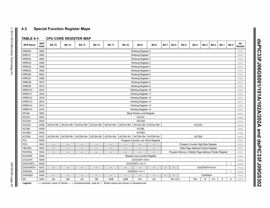
2011
-2012 Microchip T
echnology Inc.
DS
75018C
-page 43
dsP
IC33F
J06GS
001/101A/102A
/202A an
d d
sPIC
33FJ09G
S302
4.
TA
S Bit 4 Bit 3 Bit 2 Bit 1 Bit 0All
Resets
W 0000
W 0000
W 0000
W 0000
W 0000
W 0000
W 0000
W 0000
W 0000
W 0000
W 0000
W 0000
W 0000
W 0000
W 0000
W 0800
SP xxxx
AC xxxx
AC xxxx
AC ACCAU xxxx
AC xxxx
AC xxxx
AC ACCBU xxxx
PC 0000
PC ounter High Byte Register 0000
TB Address Pointer Register 0000
PS ibility Page Address Pointer Register 0000
RC xxxx
DC xxxx
DO 0 xxxx
DO DOSTARTH<5:0> 00xx
DO 0 xxxx
DO DOENDH 00xx
SR RA N OV Z C 0000
Le
3 Special Function Register Maps
BLE 4-1: CPU CORE REGISTER MAP
FR NameSFR Addr
Bit 15 Bit 14 Bit 13 Bit 12 Bit 11 Bit 10 Bit 9 Bit 8 Bit 7 Bit 6 Bit 5
REG0 0000 Working Register 0
REG1 0002 Working Register 1
REG2 0004 Working Register 2
REG3 0006 Working Register 3
REG4 0008 Working Register 4
REG5 000A Working Register 5
REG6 000C Working Register 6
REG7 000E Working Register 7
REG8 0010 Working Register 8
REG9 0012 Working Register 9
REG10 0014 Working Register 10
REG11 0016 Working Register 11
REG12 0018 Working Register 12
REG13 001A Working Register 13
REG14 001C Working Register 14
REG15 001E Working Register 15
LIM 0020 Stack Pointer Limit Register
CAL 0022 ACCAL
CAH 0024 ACCAH
CAU 0026 ACCA<39> ACCA<39> ACCA<39> ACCA<39> ACCA<39> ACCA<39> ACCA<39> ACCA<39>
CBL 0028 ACCBL
CBH 002A ACCBH
CBU 002C ACCB<39> ACCB<39> ACCB<39> ACCB<39> ACCB<39> ACCB<39> ACCB<39> ACCB<39>
L 002E Program Counter Low Word Register
H 0030 — — — — — — — — Program C
LPAG 0032 — — — — — — — — Table Page
VPAG 0034 — — — — — — — — Program Memory Vis
OUNT 0036 Repeat Loop Counter Register
OUNT 0038 DCOUNT<15:0>
STARTL 003A DOSTARTL<15:1>
STARTH 003C — — — — — — — — — —
ENDL 003E DOENDL<15:1>
ENDH 0040 — — — — — — — — — —
0042 OA OB SA SB OAB SAB DA DC IPL<2:0>
gend: x = unknown value on Reset, — = unimplemented, read as ‘0’. Reset values are shown in hexadecimal.

dsP
IC33F
J06GS
001/101A/102A
/202A an
d d
sPIC
33FJ09G
S302
DS
75018C-page 44
2011-2012 M
icrochip Technolo
gy Inc.
W ACCSAT IPL3 PSV RND IF 0020
> XWM<3:0> 0000
0 xxxx
1 xxxx
0 xxxx
1 xxxx
xxxx
xxxx
Bit 4 Bit 3 Bit 2 Bit 1 Bit 0All
Resets
CORCON 0044 — — — US EDT DL<2:0> SATA SATB SATD
MODCON 0046 XMODEN YMODEN — — BWM<3:0> YWM<3:0
XMODSRT 0048 XS<15:1>
XMODEND 004A XE<15:1>
YMODSRT 004C YS<15:1>
YMODEND 004E YE<15:1>
XBREV 0050 BREN XB<14:0>
DISICNT 0052 — — Disable Interrupts Counter Register
TABLE 4-1: CPU CORE REGISTER MAP (CONTINUED)
SFR NameSFR Addr
Bit 15 Bit 14 Bit 13 Bit 12 Bit 11 Bit 10 Bit 9 Bit 8 Bit 7 Bit 6 Bit 5
Legend: x = unknown value on Reset, — = unimplemented, read as ‘0’. Reset values are shown in hexadecimal.

2011
-2012 Microchip T
echnology Inc.
DS
75018C
-page 45
dsP
IC33F
J06GS
001/101A/102A
/202A an
d d
sPIC
33FJ09G
S302
TA 01A
TA , AND dsPIC33FJ09GS302
F it 3 Bit 2 Bit 1 Bit 0All
Resets
CN 3IE CN2IE CN1IE CN0IE 0000
CN PUE CN2PUE CN1PUE CN0PUE 0000
Le
Nit 3 Bit 2 Bit 1 Bit 0
All Resets
CN N3IE CN2IE CN1IE CN0IE 0000
CN 3PUE CN2PUE CN1PUE CN0PUE 0000
Le
BLE 4-2: CHANGE NOTIFICATION REGISTER MAP FOR dsPIC33FJ06GS001 AND dsPIC33FJ06GS1
BLE 4-3: CHANGE NOTIFICATION REGISTER MAP FOR dsPIC33FJ06GS102A, dsPIC33FJ06GS202A
ile NameSFR Addr
Bit 15 Bit 14 Bit 13 Bit 12 Bit 11 Bit 10 Bit 9 Bit 8 Bit 7 Bit 6 Bit 5 Bit 4 B
EN1 0060 — — — — — — — — CN7IE CN6IE CN5IE CN4IE CN
PU1 0068 — — — — — — — — CN7PUE CN6PUE CN5PUE CN4PUE CN3
gend: x = unknown value on Reset, — = unimplemented, read as ‘0’. Reset values are shown in hexadecimal.
File ame
SFR Addr
Bit 15 Bit 14 Bit 13 Bit 12 Bit 11 Bit 10 Bit 9 Bit 8 Bit 7 Bit 6 Bit 5 Bit 4 B
EN1 0060 CN15IE CN14IE CN13IE CN12IE CN11IE CN10IE CN9IE CN8IE CN7IE CN6IE CN5IE CN4IE C
PU1 0068 CN15PUE CN14PUE CN13PUE CN12PUE CN11PUE CN10PUE CN9PUE CN8PUE CN7PUE CN6PUE CN5PUE CN4PUE CN
gend: x = unknown value on Reset, — = unimplemented, read as ‘0’. Reset values are shown in hexadecimal.
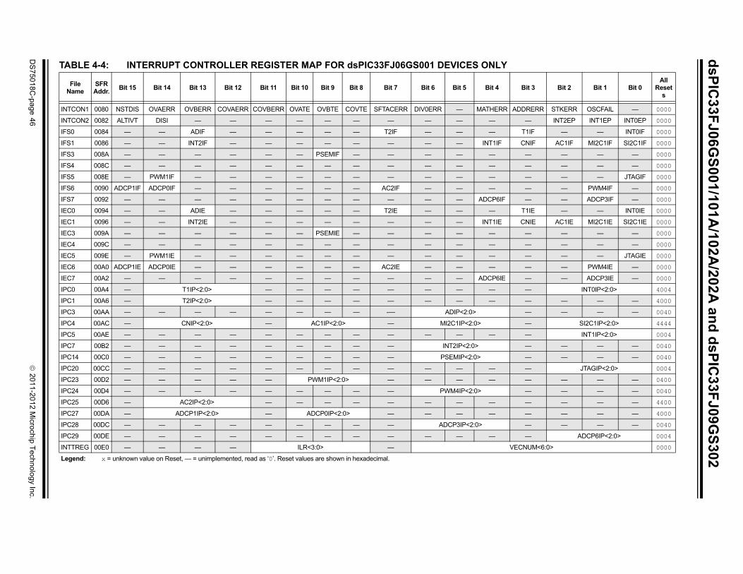
dsP
IC33F
J06GS
001/101A/102A
/202A an
d d
sPIC
33FJ09G
S302
DS
75018C-page 46
2011-2012 M
icrochip Technolo
gy Inc.
Bit 3 Bit 2 Bit 1 Bit 0All
Resets
ADDRERR STKERR OSCFAIL — 0000
— INT2EP INT1EP INT0EP 0000
T1IF — — INT0IF 0000
CNIF AC1IF MI2C1IF SI2C1IF 0000
— — — — 0000
— — — — 0000
— — — JTAGIF 0000
— — PWM4IF — 0000
— — ADCP3IF — 0000
T1IE — — INT0IE 0000
CNIE AC1IE MI2C1IE SI2C1IE 0000
— — — — 0000
— — — — 0000
— — — JTAGIE 0000
— — PWM4IE — 0000
— — ADCP3IE — 0000
— INT0IP<2:0> 4004
— — — — 4000
— — — — 0040
— SI2C1IP<2:0> 4444
— INT1IP<2:0> 0004
— — — — 0040
— — — — 0040
— JTAGIP<2:0> 0004
— — — — 0400
— — — — 0040
— — — — 4400
— — — — 4000
— — — — 0040
— ADCP6IP<2:0> 0004
VECNUM<6:0> 0000
TABLE 4-4: INTERRUPT CONTROLLER REGISTER MAP FOR dsPIC33FJ06GS001 DEVICES ONLY
File Name
SFR Addr.
Bit 15 Bit 14 Bit 13 Bit 12 Bit 11 Bit 10 Bit 9 Bit 8 Bit 7 Bit 6 Bit 5 Bit 4
INTCON1 0080 NSTDIS OVAERR OVBERR COVAERR COVBERR OVATE OVBTE COVTE SFTACERR DIV0ERR — MATHERR
INTCON2 0082 ALTIVT DISI — — — — — — — — — —
IFS0 0084 — — ADIF — — — — — T2IF — — —
IFS1 0086 — — INT2IF — — — — — — — — INT1IF
IFS3 008A — — — — — — PSEMIF — — — — —
IFS4 008C — — — — — — — — — — — —
IFS5 008E — PWM1IF — — — — — — — — — —
IFS6 0090 ADCP1IF ADCP0IF — — — — — — AC2IF — — —
IFS7 0092 — — — — — — — — — — — ADCP6IF
IEC0 0094 — — ADIE — — — — — T2IE — — —
IEC1 0096 — — INT2IE — — — — — — — — INT1IE
IEC3 009A — — — — — — PSEMIE — — — — —
IEC4 009C — — — — — — — — — — — —
IEC5 009E — PWM1IE — — — — — — — — — —
IEC6 00A0 ADCP1IE ADCP0IE — — — — — — AC2IE — — —
IEC7 00A2 — — — — — — — — — — — ADCP6IE
IPC0 00A4 — T1IP<2:0> — — — — — — — —
IPC1 00A6 — T2IP<2:0> — — — — — — — —
IPC3 00AA — — — — — — — — -— ADIP<2:0>
IPC4 00AC — CNIP<2:0> — AC1IP<2:0> — MI2C1IP<2:0>
IPC5 00AE — — — — — — — — — — — —
IPC7 00B2 — — — — — — — — — INT2IP<2:0>
IPC14 00C0 — — — — — — — — — PSEMIP<2:0>
IPC20 00CC — — — — — — — — — — — —
IPC23 00D2 — — — — — PWM1IP<2:0> — — — —
IPC24 00D4 — — — — — — — — — PWM4IP<2:0>
IPC25 00D6 — AC2IP<2:0> — — — — — — — —
IPC27 00DA — ADCP1IP<2:0> — ADCP0IP<2:0> — — — —
IPC28 00DC — — — — — — — — — ADCP3IP<2:0>
IPC29 00DE — — — — — — — — — — — —
INTTREG 00E0 — — — — ILR<3:0> —
Legend: x = unknown value on Reset, — = unimplemented, read as ‘0’. Reset values are shown in hexadecimal.

2011
-2012 Microchip T
echnology Inc.
DS
75018C
-page 47
dsP
IC33F
J06GS
001/101A/102A
/202A an
d d
sPIC
33FJ09G
S302
TA
Nit 3 Bit 2 Bit 1 Bit 0
All Resets
INT RERR STKERR OSCFAIL — 0000
INT — INT2EP INT1EP INT0EP 0000
IFS 1IF OC1IF — INT0IF 0000
IFS NIF — MI2C1IF SI2C1IF 0000
IFS — — — — 0000
IFS — — U1EIF — 0000
IFS — — — JTAGIF 0000
IFS — — PWM4IF — 0000
IFS — — ADCP3IF — 0000
IEC 1IE OC1IE — INT0IE 0000
IEC NIE — MI2C1IE SI2C1IE 0000
IEC — — — — 0000
IEC — — U1EIE — 0000
IEC — — — JTAGIE 0000
IEC — — PWM4IE — 0000
IEC — — ADCP3IE — 0000
IPC — INT0IP<2:0> 4404
IPC — — — — 4000
IPC — — — — 4440
IPC — U1TXIP<2:0> 0044
IPC — SI2C1IP<2:0> 4044
IPC — INT1IP<2:0> 0004
IPC — — — — 0040
IPC — — — — 0040
IPC — — — — 0040
IPC — JTAGIP<2:0> 0004
IPC — — — — 0400
IPC — — — — 0040
IPC — — — — 4400
IPC — — — — 0040
INT UM<6:0> 0000
Le
BLE 4-5: INTERRUPT CONTROLLER REGISTER MAP FOR dsPIC33FJ06GS101A DEVICES ONLY
File ame
SFR Addr.
Bit 15 Bit 14 Bit 13 Bit 12 Bit 11 Bit 10 Bit 9 Bit 8 Bit 7 Bit 6 Bit 5 Bit 4 B
CON1 0080 NSTDIS OVAERR OVBERR COVAERR COVBERR OVATE OVBTE COVTE SFTACERR DIV0ERR — MATHERR ADD
CON2 0082 ALTIVT DISI — — — — — — — — — —
0 0084 — — ADIF U1TXIF U1RXIF SPI1IF SPI1EIF — T2IF — — — T
1 0086 — — INT2IF — — — — — — — — INT1IF C
3 008A — — — — — — PSEMIF — — — — —
4 008C — — — — — — — — — — — —
5 008E — PWM1IF — — — — — — — — — —
6 0090 ADCP1IF ADCP0IF — — — — — — — — — —
7 0092 — — — — — — — — — — — —
0 0094 — — ADIE U1TXIE U1RXIE SPI1IE SPI1EIE — T2IE — — — T
1 0096 — — INT2IE — — — — — — — — INT1IE C
3 009A — — — — — — PSEMIE — — — — —
4 009C — — — — — — — — — — — —
5 009E — PWM1IE — — — — — — — — — —
6 00A0 ADCP1IE ADCP0IE — — — — — — — — — —
7 00A2 — — — — — — — — — — — —
0 00A4 — T1IP<2:0> — OC1IP<2:0> — — — —
1 00A6 — T2IP<2:0> — — — — — — — —
2 00A8 — U1RXIP<2:0> — SPI1IP<2:0> — SPI1EIP<2:0>
3 00AA — — — — — — — — -— ADIP<2:0>
4 00AC — CNIP<2:0> — — — — — MI2C1IP<2:0>
5 00AE — — — — — — — — — — — —
7 00B2 — — — — — — — — — INT2IP<2:0>
14 00C0 — — — — — — — — — PSEMIP<2:0>
16 00C4 — — — — — — — — — U1EIP<2:0>
20 00CC — — — — — — — — — — — —
23 00D2 — — — — — PWM1IP<2:0> — — — —
24 00D4 — — — — — — — — — PWM4IP<2:0>
27 00DA — ADCP1IP<2:0> — ADCP0IP<2:0> — — — —
28 00DC — — — — — — — — — ADCP3IP<2:0>
TREG 00E0 — — — — ILR<3:0> — VECN
gend: x = unknown value on Reset, — = unimplemented, read as ‘0’. Reset values are shown in hexadecimal.

dsP
IC33F
J06GS
001/101A/102A
/202A an
d d
sPIC
33FJ09G
S302
DS
75018C-page 48
2011-2012 M
icrochip Technolo
gy Inc.
Y
Bit 3 Bit 2 Bit 1 Bit 0All
Resets
ADDRERR STKERR OSCFAIL — 0000
— INT2EP INT1EP INT0EP 0000
T1IF OC1IF — INT0IF 0000
CNIF — MI2C1IF SI2C1IF 0000
— — — — 0000
— — U1EIF — 0000
— — — JTAGIF 0000
— — — — 0000
— — — ADCP2IF 0000
T1IE OC1IE — INT0IE 0000
CNIE — MI2C1IE SI2C1IE 0000
— — — — 0000
— — U1EIE — 0000
— — — JTAGIE 0000
— — — — 0000
— — — ADCP2IE 0000
— INT0IP<2:0> 4404
— — — — 4000
— — — — 4440
— U1TXIP<2:0> 0044
— SI2C1IP<2:0> 4044
— INT1IP<2:0> 0004
— — — — 0040
— — — — 0040
— — — — 0040
— JTAGIP<2:0> 0004
— — — — 4400
— — — — 4400
— ADCP2IP<2:0> 0004
VECNUM<6:0> 0000
TABLE 4-6: INTERRUPT CONTROLLER REGISTER MAP FOR dsPIC33FJ06GS102A DEVICES ONL
File Name
SFR Addr.
Bit 15 Bit 14 Bit 13 Bit 12 Bit 11 Bit 10 Bit 9 Bit 8 Bit 7 Bit 6 Bit 5 Bit 4
INTCON1 0080 NSTDIS OVAERR OVBERR COVAERR COVBERR OVATE OVBTE COVTE SFTACERR DIV0ERR — MATHERR
INTCON2 0082 ALTIVT DISI — — — — — — — — — —
IFS0 0084 — — ADIF U1TXIF U1RXIF SPI1IF SPI1EIF — T2IF — — —
IFS1 0086 — — INT2IF — — — — — — — — INT1IF
IFS3 008A — — — — — — PSEMIF — — — — —
IFS4 008C — — — — — — — — — — — —
IFS5 008E PWM2IF PWM1IF — — — — — — — — — —
IFS6 0090 ADCP1IF ADCP0IF — — — — — — — — — —
IFS7 0092 — — — — — — — — — — — —
IEC0 0094 — — ADIE U1TXIE U1RXIE SPI1IE SPI1EIE — T2IE — — —
IEC1 0096 — — INT2IE — — — — — — — — INT1IE
IEC3 009A — — — — — — PSEMIE — — — — —
IEC4 009C — — — — — — — — — — — —
IEC5 009E PWM2IE PWM1IE — — — — — — — — — —
IEC6 00A0 ADCP1IE ADCP0IE — — — — — — — — — —
IEC7 00A2 — — — — — — — — — — — —
IPC0 00A4 — T1IP<2:0> — OC1IP<2:0> — — — —
IPC1 00A6 — T2IP<2:0> — — — — — — — —
IPC2 00A8 — U1RXIP<2:0> — SPI1IP<2:0> — SPI1EIP<2:0>
IPC3 00AA — — — — — — — — -— ADIP<2:0>
IPC4 00AC — CNIP<2:0> — — — — — MI2C1IP<2:0>
IPC5 00AE — — — — — — — — — — — —
IPC7 00B2 — — — — — — — — — INT2IP<2:0>
IPC14 00C0 — — — — — — — — — PSEMIP<2:0>
IPC16 00C4 — — — — — — — — — U1EIP<2:0>
IPC20 00CC — — — — — — — — — — — —
IPC23 00D2 — PWM2IP<2:0> — PWM1IP<2:0> — — — —
IPC27 00DA — ADCP1IP<2:0> — ADCP0IP<2:0> — — — —
IPC28 00DC — — — — — — — — — — — —
INTTREG 00E0 — — — — ILR<3:0> —
Legend: x = unknown value on Reset, — = unimplemented, read as ‘0’. Reset values are shown in hexadecimal.

2011
-2012 Microchip T
echnology Inc.
DS
75018C
-page 49
dsP
IC33F
J06GS
001/101A/102A
/202A an
d d
sPIC
33FJ09G
S302
TA
Nit 3 Bit 2 Bit 1 Bit 0
All Resets
INT RERR STKERR OSCFAIL — 0000
INT — INT2EP INT1EP INT0EP 0000
IFS 1IF OC1IF IC1IF INT0IF 0000
IFS NIF AC1IF MI2C1IF SI2C1IF 0000
IFS — — — — 0000
IFS — — U1EIF — 0000
IFS — — — JTAGIF 0000
IFS — — — — 0000
IFS — — — ADCP2IF 0000
IEC 1IE OC1IE IC1IE INT0IE 0000
IEC NIE AC1IE MI2C1IE SI2C1IE 0000
IEC — — — — 0000
IEC — — U1EIE — 0000
IEC — — — JTAGIE 0000
IEC — — — — 0000
IEC — — — ADCP2IE 0000
IPC — INT0IP<2:0> 4444
IPC — — — — 4000
IPC — — — — 4440
IPC — U1TXIP<2:0> 0044
IPC — SI2C1IP<2:0> 4444
IPC — INT1IP<2:0> 0004
IPC — — — — 0040
IPC — — — — 0040
IPC — — — — 0040
IPC — JTAGIP<2:0> 0004
IPC — — — — 4400
IPC — — — — 4000
IPC — — — — 4400
IPC — ADCP2IP<2:0> 0004
IPC — ADCP6IP<2:0> 0004
INT UM<6:0> 0000
Le
BLE 4-7: INTERRUPT CONTROLLER REGISTER MAP FOR dsPIC33FJ06GS202A DEVICES ONLY
File ame
SFR Addr.
Bit 15 Bit 14 Bit 13 Bit 12 Bit 11 Bit 10 Bit 9 Bit 8 Bit 7 Bit 6 Bit 5 Bit 4 B
CON1 0080 NSTDIS OVAERR OVBERR COVAERR COVBERR OVATE OVBTE COVTE SFTACERR DIV0ERR — MATHERR ADD
CON2 0082 ALTIVT DISI — — — — — — — — — —
0 0084 — — ADIF U1TXIF U1RXIF SPI1IF SPI1EIF — T2IF — — — T
1 0086 — — INT2IF — — — — — — — — INT1IF C
3 008A — — — — — — PSEMIF — — — — —
4 008C — — — — — — — — — — — —
5 008E PWM2IF PWM1IF — — — — — — — — — —
6 0090 ADCP1IF ADCP0IF — — — — — — AC2IF — — —
7 0092 — — — — — — — — — — — ADCP6IF
0 0094 — — ADIE U1TXIE U1RXIE SPI1IE SPI1EIE — T2IE — — — T
1 0096 — — INT2IE — — — — — — — — INT1IE C
3 009A — — — — — — PSEMIE — — — — —
4 009C — — — — — — — — — — — —
5 009E PWM2IE PWM1IE — — — — — — — — — —
6 00A0 ADCP1IE ADCP0IE — — — — — — AC2IE — — —
7 00A2 — — — — — — — — — — — ADCP6IE
0 00A4 — T1IP<2:0> — OC1IP<2:0> — IC1IP<2:0>
1 00A6 — T2IP<2:0> — — — — — — — —
2 00A8 — U1RXIP<2:0> — SPI1IP<2:0> — SPI1EIP<2:0>
3 00AA — — — — — — — — -— ADIP<2:0>
4 00AC — CNIP<2:0> — AC1IP<2:0> — MI2C1IP<2:0>
5 00AE — — — — — — — — — — — —
7 00B2 — — — — — — — — — INT2IP<2:0>
14 00C0 — — — — — — — — — PSEMIP<2:0>
16 00C4 — — — — — — — — — U1EIP<2:0>
20 00CC — — — — — — — — — — — —
23 00D2 — PWM2IP<2:0> — PWM1IP<2:0> — — — —
25 00D6 — AC2IP<2:0> — — — — — — — —
27 00DA — ADCP1IP<2:0> — ADCP0IP<2:0> — — — —
28 00DC — — — — — — — — — — — —
29 00DE — — — — — — — — — — — —
TREG 00E0 — — — — ILR<3:0> — VECN
gend: x = unknown value on Reset, — = unimplemented, read as ‘0’. Reset values are shown in hexadecimal.

dsP
IC33F
J06GS
001/101A/102A
/202A an
d d
sPIC
33FJ09G
S302
DS
75018C-page 50
2011-2012 M
icrochip Technolo
gy Inc.
Bit 3 Bit 2 Bit 1 Bit 0All
Resets
ADDRERR STKERR OSCFAIL — 0000
— INT2EP INT1EP INT0EP 0000
T1IF OC1IF IC1IF INT0IF 0000
CNIF AC1IF MI2C1IF SI2C1IF 0000
— — — — 0000
— — U1EIF — 0000
— — — JTAGIF 0000
— — PWM4IF — 0000
— — ADCP3IF ADCP2IF 0000
T1IE OC1IE IC1IE INT0IE 0000
CNIE AC1IE MI2C1IE SI2C1IE 0000
— — — — 0000
— — U1EIE — 0000
— — — JTAGIE 0000
— — PWM4IE — 0000
— — ADCP3IE ADCP2IE 0000
— INT0IP<2:0> 4444
-— — — — 4000
— — — — 4440
— U1TXIP<2:0> 0044
— SI2C1IP<2:0> 4444
— INT1IP<2:0> 0004
— — — — 0040
— — — — 0040
— — — — 0040
— JTAGIP<2:0> 0004
— — — — 4400
— — — — 0040
— — — — 4000
— — — — 4400
— ADCP2IP<2:0> 0044
— ADCP6IP<2:0> 0004
VECNUM<6:0> 0000
TABLE 4-8: INTERRUPT CONTROLLER REGISTER MAP FOR dsPIC33FJ09GS302 DEVICES ONLY
File Name
SFR Addr.
Bit 15 Bit 14 Bit 13 Bit 12 Bit 11 Bit 10 Bit 9 Bit 8 Bit 7 Bit 6 Bit 5 Bit 4
INTCON1 0080 NSTDIS OVAERR OVBERR COVAERR COVBERR OVATE OVBTE COVTE SFTACERR DIV0ERR — MATHERR
INTCON2 0082 ALTIVT DISI — — — — — — — — — —
IFS0 0084 — — ADIF U1TXIF U1RXIF SPI1IF SPI1EIF — T2IF — — —
IFS1 0086 — — INT2IF — — — — — — — — INT1IF
IFS3 008A — — — — — — PSEMIF — — — — —
IFS4 008C — — — — — — — — — — — —
IFS5 008E PWM2IF PWM1IF — — — — — — — — — —
IFS6 0090 ADCP1IF ADCP0IF — — — — — — AC2IF — — —
IFS7 0092 — — — — — — — — — — — ADCP6IF
IEC0 0094 — — ADIE U1TXIE U1RXIE SPI1IE SPI1EIE — T2IE — — —
IEC1 0096 — — INT2IE — — — — — — — — INT1IE
IEC3 009A — — — — — — PSEMIE — — — — —
IEC4 009C — — — — — — — — — — — —
IEC5 009E PWM2IE PWM1IE — — — — — — — — — —
IEC6 00A0 ADCP1IE ADCP0IE — — — — — — AC2IE — — —
IEC7 00A2 — — — — — — — — — — — ADCP6IE
IPC0 00A4 — T1IP<2:0> — OC1IP<2:0> — IC1IP<2:0>
IPC1 00A6 — T2IP<2:0> — — — — — — — —
IPC2 00A8 — U1RXIP<2:0> — SPI1IP<2:0> — SPI1EIP<2:0>
IPC3 00AA — — — — -— — -— ADIP<2:0>
IPC4 00AC — CNIP<2:0> — AC1IP<2:0> — MI2C1IP<2:0>
IPC5 00AE — — — — — — — — — — — —
IPC7 00B2 — — — — — — — — — INT2IP<2:0>
IPC14 00C0 — — — — — — — — — PSEMIP<2:0>
IPC16 00C4 — — — — — — — — — U1EIP<2:0>
IPC20 00CC — — — — — — — — — — — —
IPC23 00D2 — PWM2IP<2:0> — PWM1IP<2:0> — — — —
IPC24 00D4 — — — — — — — — — PWM4IP<2:0>
IPC25 00D6 — AC2IP<2:0> — — — — — — — —
IPC27 00DA — ADCP1IP<2:0> — ADCP0IP<2:0> -— —
IPC28 00DC — — — — — — — — — ADCP3IP<2:0>
IPC29 00DE — — — — — — — — — — — —
INTTREG 00E0 — — — — ILR<3:0> —
Legend: x = unknown value on Reset, — = unimplemented, read as ‘0’. Reset values are shown in hexadecimal.

2011
-2012 Microchip T
echnology Inc.
DS
75018C
-page 51
dsP
IC33F
J06GS
001/101A/102A
/202A an
d d
sPIC
33FJ09G
S302
TA
TA
NBit 3 Bit 2 Bit 1 Bit 0
All Resets
TM 0000
PR FFFF
T1 — TSYNC TCS — 0000
TM 0000
PR FFFF
T2 — — TCS — 0000
Le
Nt 3 Bit 2 Bit 1 Bit 0
All Resets
IC xxxx
IC NE ICM<2:0> 0000
Le
TA PIC33FJ06GS202A
NBit 3 Bit 2 Bit 1 Bit 0
All Resets
OC xxxx
OC xxxx
OC — OCM<2:0> 0000
Le
BLE 4-9: TIMER REGISTER MAP
BLE 4-10: INPUT CAPTURE REGISTER MAP FOR dsPIC33FJ06GS202A AND dsPIC33FJ09GS302
SFR ame
SFR Addr
Bit 15 Bit 14 Bit 13 Bit 12 Bit 11 Bit 10 Bit 9 Bit 8 Bit 7 Bit 6 Bit 5 Bit 4
R1 0100 Timer1 Register
1 0102 Period Register 1
CON 0104 TON — TSIDL — — — — — — TGATE TCKPS<1:0>
R2 0106 Timer2 Register
2 010C Period Register 2
CON 0110 TON — TSIDL — — — — — — TGATE TCKPS<1:0>
gend: x = unknown value on Reset, — = unimplemented, read as ‘0’. Reset values are shown in hexadecimal.
SFR ame
SFR Addr Bit 15 Bit 14 Bit 13 Bit 12 Bit 11 Bit 10 Bit 9 Bit 8 Bit 7 Bit 6 Bit 5 Bit 4 Bi
1BUF 0140 Input Capture 1 Register
1CON 0142 — — ICSIDL — — — — — — ICI<1:0> ICOV ICB
gend: x = unknown value on Reset, — = unimplemented, read as ‘0’. Reset values are shown in hexadecimal.
BLE 4-11: OUTPUT COMPARE REGISTER MAP FOR dsPIC33FJ06GS101A, dsPIC33FJ06GS102A, dsAND dsPIC33FJ09GS302
SFR ame
SFR Addr
Bit 15 Bit 14 Bit 13 Bit 12 Bit 11 Bit 10 Bit 9 Bit 8 Bit 7 Bit 6 Bit 5 Bit 4
1RS 0180 Output Compare 1 Secondary Register
1R 0182 Output Compare 1 Register
1CON 0184 — — OCSIDL — — — — — — — — OCFLT
gend: x = unknown value on Reset, — = unimplemented, read as ‘0’. Reset values are shown in hexadecimal.

dsP
IC33F
J06GS
001/101A/102A
/202A an
d d
sPIC
33FJ09G
S302
DS
75018C-page 52
2011-2012 M
icrochip Technolo
gy Inc.
Bit 4 Bit 3 Bit 2 Bit 1 Bit 0All
Resets
C<1:0> SEVTPS<3:0> 0000
— — PCLKDIV<2:0> 0000
FFF8
— — — 0000
0000
— — — 0000
4 Bit 3 Bit 2 Bit 1 Bit 0All
Resets
— CAM XPRES IUE 0000
CLDAT<1:0> SWAP OSYNC 0000
FLTPOL FLTMOD<1:0> 0000
0000
0000
0000
0000
0000
0000
— — — 0000
TRGSTRT<5:0> 0000
— — — 0000
— — — 0000
— — — 0000
PSEL<3:0> CHOPHEN CHOPLEN 0000
TABLE 4-12: HIGH-SPEED PWM REGISTER MAP
File NameAddr Offset
Bit 15 Bit 14 Bit 13 Bit 12 Bit 11 Bit 10 Bit 9 Bit 8 Bit 7 Bit 6 Bit 5
PTCON 0400 PTEN — PTSIDL SESTAT SEIEN EIPU SYNCPOL SYNCOEN SYNCEN — SYNCSR
PTCON2 0402 — — — — — — — — — — —
PTPER 0404 PTPER<15:0>
SEVTCMP 0406 SEVTCMP<15:3>
MDC 040A MDC<15:0>
CHOP 041A CHPCLKEN — — — — — CHOPCLK<6:0>
Legend: x = unknown value on Reset, — = unimplemented, read as ‘0’. Reset values are shown in hexadecimal.
TABLE 4-13: HIGH-SPEED PWM GENERATOR 1 REGISTER MAP
File NameAddr Offset
Bit 15 Bit 14 Bit 13 Bit 12 Bit 11 Bit 10 Bit 9 Bit 8 Bit 7 Bit 6 Bit 5 Bit
PWMCON1 0420 FLTSTAT CLSTAT TRGSTAT FLTIEN CLIEN TRGIEN ITB MDCS DTC<1:0> — —
IOCON1 0422 PENH PENL POLH POLL PMOD<1:0> OVRENH OVRENL OVRDAT<1:0> FLTDAT<1:0>
FCLCON1 0424 IFLTMOD CLSRC<4:0> CLPOL CLMOD FLTSRC<4:0>
PDC1 0426 PDC1<15:0>
PHASE1 0428 PHASE1<15:0>
DTR1 042A — — DTR1<13:0>
ALTDTR1 042C — — ALTDTR1<13:0>
SDC1 042E SDC1<15:0>
SPHASE1 0430 SPHASE1<15:0>
TRIG1 0432 TRGCMP<15:3>
TRGCON1 0434 TRGDIV<3:0> — — — — DTM —
STRIG1 0436 STRGCMP<15:3>
PWMCAP1 0438 PWMCAP1<15:3>
LEBCON1 043A PHR PHF PLR PLF FLTLEBEN CLLEBEN LEB<6:0>
AUXCON1 043E HRPDIS HRDDIS — — — — — — — — CHO
Legend: x = unknown value on Reset, — = unimplemented, read as ‘0’. Reset values are shown in hexadecimal.

2011
-2012 Microchip T
echnology Inc.
DS
75018C
-page 53
dsP
IC33F
J06GS
001/101A/102A
/202A an
d d
sPIC
33FJ09G
S302
TA S202A AND dsPIC33FJ09GS302
Fi it 3 Bit 2 Bit 1 Bit 0All
Resets
PW CAM XPRES IUE 0000
IO LDAT<1:0> SWAP OSYNC 0000
FC FLTPOL FLTMOD<1:0> 0000
PD 0000
PH 0000
DT 0000
AL 0000
SD 0000
SP 0000
TR — — — 0000
TR TRGSTRT<5:0> 0000
ST — — — 0000
PW — — — 0000
LE — — — 0000
AU 3:0> CHOPHEN CHOPLEN 0000
Le
BLE 4-14: HIGH-SPEED PWM GENERATOR 2 REGISTER MAP FOR dsPIC33FJ06GS102A, dsPIC33FJ06G
le NameAddr Offset
Bit 15 Bit 14 Bit 13 Bit 12 Bit 11 Bit 10 Bit 9 Bit 8 Bit 7 Bit 6 Bit 5 Bit 4 B
MCON2 0440 FLTSTAT CLSTAT TRGSTAT FLTIEN CLIEN TRGIEN ITB MDCS DTC<1:0> — — —
CON2 0442 PENH PENL POLH POLL PMOD<1:0> OVRENH OVRENL OVRDAT<1:0> FLTDAT<1:0> C
LCON2 0444 IFLTMOD CLSRC<4:0> CLPOL CLMOD FLTSRC<4:0>
C2 0446 PDC2<15:0>
ASE2 0448 PHASE2<15:0>
R2 044A — — DTR2<13:0>
TDTR2 044C — — ALTDTR2<13:0>
C2 044E SDC2<15:0>
HASE2 0450 SPHASE2<15:0>
IG2 0452 TRGCMP<15:3>
GCON2 0454 TRGDIV<3:0> — — — — DTM —
RIG2 0456 STRGCMP<15:3>
MCAP2 0458 PWMCAP2<15:3>
BCON2 045A PHR PHF PLR PLF FLTLEBEN CLLEBEN LEB<6:0>
XCON2 045E HRPDIS HRDDIS — — — — — — — — CHOPSEL<
gend: x = unknown value on Reset, — = unimplemented, read as ‘0’. Reset values are shown in hexadecimal.

dsP
IC33F
J06GS
001/101A/102A
/202A an
d d
sPIC
33FJ09G
S302
DS
75018C-page 54
2011-2012 M
icrochip Technolo
gy Inc.
J06GS101A AND
Bit 3 Bit 2 Bit 1 Bit 0All
Resets
— CAM XPRES IUE 0000
CLDAT<1:0> SWAP OSYNC 0000
FLTPOL FLTMOD<1:0> 0000
0000
0000
0000
0000
0000
0000
— — — 0000
TRGSTRT<5:0> 0000
— — — 0000
— — — 0000
— — — 0000
EL<3:0> CHOPHEN CHOPLEN 0000
TABLE 4-15: HIGH-SPEED PWM GENERATOR 4 REGISTER MAP FOR dsPIC33FJ06GS001, dsPIC33FdsPIC33FJ09GS302
File NameAddr Offset
Bit 15 Bit 14 Bit 13 Bit 12 Bit 11 Bit 10 Bit 9 Bit 8 Bit 7 Bit 6 Bit 5 Bit 4
PWMCON4 0480 FLTSTAT CLSTAT TRGSTAT FLTIEN CLIEN TRGIEN ITB MDCS DTC<1:0> — —
IOCON4 0482 PENH PENL POLH POLL PMOD<1:0> OVRENH OVRENL OVRDAT<1:0> FLTDAT<1:0>
FCLCON4 0484 IFLTMOD CLSRC<4:0> CLPOL CLMOD FLTSRC<4:0>
PDC4 0486 PDC4<15:0>
PHASE4 0488 PHASE4<15:0>
DTR4 048A — — DTR4<13:0>
ALTDTR4 048C — — ALTDTR4<13:0>
SDC4 048E SDC4<15:0>
SPHASE4 0490 SPHASE4<15:0>
TRIG4 0492 TRGCMP<15:3>
TRGCON4 0494 TRGDIV<3:0> — — — — DTM —
STRIG4 0496 STRGCMP<15:3>
PWMCAP4 0498 PWMCAP4<15:3>
LEBCON4 049A PHR PHF PLR PLF FLTLEBEN CLLEBEN LEB<6:0>
AUXCON4 049E HRPDIS HRDDIS — — — — — — — — CHOPS
Legend: x = unknown value on Reset, — = unimplemented, read as ‘0’. Reset values are shown in hexadecimal.

2011
-2012 Microchip T
echnology Inc.
DS
75018C
-page 55
dsP
IC33F
J06GS
001/101A/102A
/202A an
d d
sPIC
33FJ09G
S302
TA 02A AND dsPIC33FJ09GS302
TA A AND dsPIC33FJ09GS302
TA
N 3 Bit 2 Bit 1 Bit 0
All Resets
I2C er 0000
I2C er 00FF
I2C ter 0000
I2C EN PEN RSEN SEN 1000
I2C R_W RBF TBF 0000
I2C 0000
I2C 0000
Le
SF 3 Bit 2 Bit 1 Bit 0All
Resets
U1 GH PDSEL<1:0> STSEL 0000
U1 RR FERR OERR URXDA 0110
U1 r xxxx
U1 0000
U1 0000
Le
SF it 3 Bit 2 Bit 1 Bit 0All
Resets
SP — — SPITBF SPIRBF 0000
SP E<2:0> PPRE<1:0> 0000
SP — — FRMDLY — 0000
SP 0000
Le
BLE 4-17: UART1 REGISTER MAP FOR dsPIC33FJ06GS101A, dsPIC33FJ06GS102A, dsPIC33FJ06GS2
BLE 4-18: SPI1 REGISTER MAP FOR dsPIC33FJ06GS101A, dsPIC33FJ06GS102A, dsPIC33FJ06GS202
BLE 4-16: I2C1 REGISTER MAP
SFR ame
SFR Addr
Bit 15 Bit 14 Bit 13 Bit 12 Bit 11 Bit 10 Bit 9 Bit 8 Bit 7 Bit 6 Bit 5 Bit 4 Bit
1RCV 0200 — — — — — — — — Receive Regist
1TRN 0202 — — — — — — — — Transmit Regist
1BRG 0204 — — — — — — — Baud Rate Generator Regis
1CON 0206 I2CEN — I2CSIDL SCLREL IPMIEN A10M DISSLW SMEN GCEN STREN ACKDT ACKEN RC
1STAT 0208 ACKSTAT TRSTAT — — — BCL GCSTAT ADD10 IWCOL I2COV D_A P S
1ADD 020A — — — — — — Address Register
1MSK 020C — — — — — — AMSK<9:0>
gend: x = unknown value on Reset, — = unimplemented, read as ‘0’. Reset values are shown in hexadecimal.
R NameSFR Addr
Bit 15 Bit 14 Bit 13 Bit 12 Bit 11 Bit 10 Bit 9 Bit 8 Bit 7 Bit 6 Bit 5 Bit 4 Bit
MODE 0220 UARTEN — USIDL IREN RTSMD — UEN1 UEN0 WAKE LPBACK ABAUD URXINV BR
STA 0222 UTXISEL1 UTXINV UTXISEL0 — UTXBRK UTXEN UTXBF TRMT URXISEL<1:0> ADDEN RIDLE PE
TXREG 0224 — — — — — — — UART Transmit Registe
RXREG 0226 — — — — — — — UART Receive Register
BRG 0228 Baud Rate Generator Prescaler
gend: x = unknown value on Reset, — = unimplemented, read as ‘0’. Reset values are shown in hexadecimal.
R NameSFR Addr
Bit 15 Bit 14 Bit 13 Bit 12 Bit 11 Bit 10 Bit 9 Bit 8 Bit 7 Bit 6 Bit 5 Bit 4 B
I1STAT 0240 SPIEN — SPISIDL — — — — — — SPIROV — —
I1CON1 0242 — — — DISSCK DISSDO MODE16 SMP CKE SSEN CKP MSTEN SPR
I1CON2 0244 FRMEN SPIFSD FRMPOL — — — — — — — — —
I1BUF 0248 SPI1 Transmit and Receive Buffer Register
gend: x = unknown value on Reset, — = unimplemented, read as ‘0’. Reset values are shown in hexadecimal.

dsP
IC33F
J06GS
001/101A/102A
/202A an
d d
sPIC
33FJ09G
S302
DS
75018C-page 56
2011-2012 M
icrochip Technolo
gy Inc.
GS101A
Bit 3 Bit 2 Bit 1 Bit 0All
Resets
ISRCCAL<5:0> 0000
t 4 Bit 3 Bit 2 Bit 1 Bit 0All
Resets
SAMP — ADCS<2:0> 0003
PCFG3 PCFG2 PCFG1 PCFG0 0000
P3RDY — P1RDY P0RDY 0000
— 0000
TRGSRC0<4:0> 0000
— — — — 0000
TRGSRC6<4:0> 0000
xxxx
xxxx
xxxx
xxxx
xxxx
xxxx
xxxx
xxxx
TABLE 4-19: CONSTANT CURRENT SOURCE REGISTER MAP
TABLE 4-20: HIGH-SPEED 10-BIT ADC REGISTER MAP FOR dsPIC33FJ06GS001 AND dsPIC33FJ06
File Name ADR Bit 15 Bit 14 Bit 13 Bit 12 Bit 11 Bit 10 Bit 9 Bit 8 Bit 7 Bit 6 Bit 5 Bit 4
ISRCCON 0500 ISRCEN — — — — OUTSEL<2:0> — —
Legend: x = unknown value on Reset, — = unimplemented, read as ‘0’. Reset values are shown in hexadecimal.
SFR NameSFR Addr
Bit 15 Bit 14 Bit 13 Bit 12 Bit 11 Bit 10 Bit 9 Bit 8 Bit 7 Bit 6 Bit 5 Bi
ADCON 0300 ADON — ADSIDL SLOWCLK — GSWTRG — FORM EIE ORDER SEQSAMP ASYNC
ADPCFG 0302 — — — — — — — — PCFG7 PCFG6 — —
ADSTAT 0306 — — — — — — — — — P6RDY — —
ADBASE 0308 ADBASE<15:1>
ADCPC0 030A IRQEN1 PEND1 SWTRG1 TRGSRC1<4:0> IRQEN0 PEND0 SWTRG0
ADCPC1 030C IRQEN3 PEND3 SWTRG3 TRGSRC3<4:0> — — — —
ADCPC3 0310 — — — — — — — — IRQEN6 PEND6 SWTRG6
ADCBUF0 0320 ADC Data Buffer 0
ADCBUF1 0322 ADC Data Buffer 1
ADCBUF2 0324 ADC Data Buffer 2
ADCBUF3 0326 ADC Data Buffer 3
ADCBUF6 032C ADC Data Buffer 6
ADCBUF7 032E ADC Data Buffer 7
ADCBUF12 0338 ADC Data Buffer 12
ADCBUF13 033A ADC Data Buffer 13
Legend: x = unknown value on Reset, — = unimplemented, read as ‘0’. Reset values are shown in hexadecimal.

2011
-2012 Microchip T
echnology Inc.
DS
75018C
-page 57
dsP
IC33F
J06GS
001/101A/102A
/202A an
d d
sPIC
33FJ09G
S302
TA S202A
SF Bit 3 Bit 2 Bit 1 Bit 0All
Resets
AD P — ADCS<2:0> 0003
AD PCFG3 PCFG2 PCFG1 PCFG0 0000
AD — P2RDY P1RDY P0RDY 0000
AD — 0000
AD TRGSRC0<4:0> 0000
AD TRGSRC2<4:0> 0000
AD TRGSRC6<4:0> 0000
AD xxxx
AD xxxx
AD xxxx
AD xxxx
AD xxxx
AD xxxx
AD xxxx
AD xxxx
Le
BLE 4-21: HIGH-SPEED 10-BIT ADC REGISTER MAP FOR dsPIC33FJ06GS102A AND dsPIC33FJ06G
R NameSFR Addr
Bit 15 Bit 14 Bit 13 Bit 12 Bit 11 Bit 10 Bit 9 Bit 8 Bit 7 Bit 6 Bit 5 Bit 4
CON 0300 ADON — ADSIDL SLOWCLK — GSWTRG — FORM EIE ORDER SEQSAMP ASYNCSAM
PCFG 0302 — — — — — — — — — — PCFG5 PCFG4
STAT 0306 — — — — — — — — — P6RDY — —
BASE 0308 ADBASE<15:1>
CPC0 030A IRQEN1 PEND1 SWTRG1 TRGSRC1<4:0> IRQEN0 PEND0 SWTRG0
CPC1 030C — — — — — — — — IRQEN2 PEND2 SWTRG2
CPC3 0310 — — — — — — — — IRQEN6 PEND6 SWTRG6
CBUF0 0320 ADC Data Buffer 0
CBUF1 0322 ADC Data Buffer 1
CBUF2 0324 ADC Data Buffer 2
CBUF3 0326 ADC Data Buffer 3
CBUF4 0328 ADC Data Buffer 4
CBUF5 032A ADC Data Buffer 5
CBUF12 0338 ADC Data Buffer 12
CBUF13 033A ADC Data Buffer 13
gend: x = unknown value on Reset, — = unimplemented, read as ‘0’. Reset values are shown in hexadecimal.

dsP
IC33F
J06GS
001/101A/102A
/202A an
d d
sPIC
33FJ09G
S302
DS
75018C-page 58
2011-2012 M
icrochip Technolo
gy Inc.
FJ06GS202A AND dsPIC33FJ09GS302
t 4 Bit 3 Bit 2 Bit 1 Bit 0All
Resets
SAMP — ADCS<2:0> 0003
G4 PCFG3 PCFG2 PCFG1 PCFG0 0000
P3RDY P2RDY P1RDY P0RDY 0000
— 0000
TRGSRC0<4:0> 0000
TRGSRC2<4:0> 0000
TRGSRC6<4:0> 0000
xxxx
xxxx
xxxx
xxxx
xxxx
xxxx
xxxx
xxxx
xxxx
xxxx
Bit 3 Bit 2 Bit 1 Bit 0All
Resets
L CMPSTAT HGAIN CMPPOL RANGE 0000
0000
L CMPSTAT HGAIN CMPPOL RANGE 0000
0000
TABLE 4-22: HIGH-SPEED 10-BIT ADC REGISTER MAP FOR dsPIC33FJ09GS302
TABLE 4-23: ANALOG COMPARATOR CONTROL REGISTER MAP FOR dsPIC33FJ06GS001, dsPIC33
SFR NameSFR Addr
Bit 15 Bit 14 Bit 13 Bit 12 Bit 11 Bit 10 Bit 9 Bit 8 Bit 7 Bit 6 Bit 5 Bi
ADCON 0300 ADON — ADSIDL SLOWCLK — GSWTRG — FORM EIE ORDER SEQSAMP ASYNC
ADPCFG 0302 — — — — — — — — PCFG7 PCFG6 PCFG5 PCF
ADSTAT 0306 — — — — — — — — — P6RDY — —
ADBASE 0308 ADBASE<15:1>
ADCPC0 030A IRQEN1 PEND1 SWTRG1 TRGSRC1<4:0> IRQEN0 PEND0 SWTRG0
ADCPC1 030C IRQEN3 PEND3 SWTRG3 TRGSRC3<4:0> IRQEN2 PEND2 SWTRG2
ADCPC3 0310 — — — — — — — — IRQEN6 PEND6 SWTRG6
ADCBUF0 0320 ADC Data Buffer 0
ADCBUF1 0322 ADC Data Buffer 1
ADCBUF2 0324 ADC Data Buffer 2
ADCBUF3 0326 ADC Data Buffer 3
ADCBUF4 0328 ADC Data Buffer 4
ADCBUF5 032A ADC Data Buffer 5
ADCBUF6 032C ADC Data Buffer 6
ADCBUF7 032E ADC Data Buffer 7
ADCBUF12 0338 ADC Data Buffer 12
ADCBUF13 033A ADC Data Buffer 13
Legend: x = unknown value on Reset, — = unimplemented, read as ‘0’. Reset values are shown in hexadecimal.
File Name ADR Bit 15 Bit 14 Bit 13 Bit 12 Bit 11 Bit 10 Bit 9 Bit 8 Bit 7 Bit 6 Bit 5 Bit 4
CMPCON1 0540 CMPON — CMPSIDL HYSSEL<1:0> FLTREN FCLKSEL DACOE(1) INSEL<1:0> EXTREF HYSPO
CMPDAC1 0542 — — — — — — CMREF<9:0>
CMPCON2 0544 CMPON — CMPSIDL HYSSEL<1:0> FLTREN FCLKSEL DACOE(1) INSEL<1:0> EXTREF HYSPO
CMPDAC2 0546 — — — — — — CMREF<9:0>
Legend: x = unknown value on Reset, — = unimplemented, read as ‘0’. Reset values are shown in hexadecimal.Note 1: This bit is not available in the dsPIC33FJ06GS001 device.
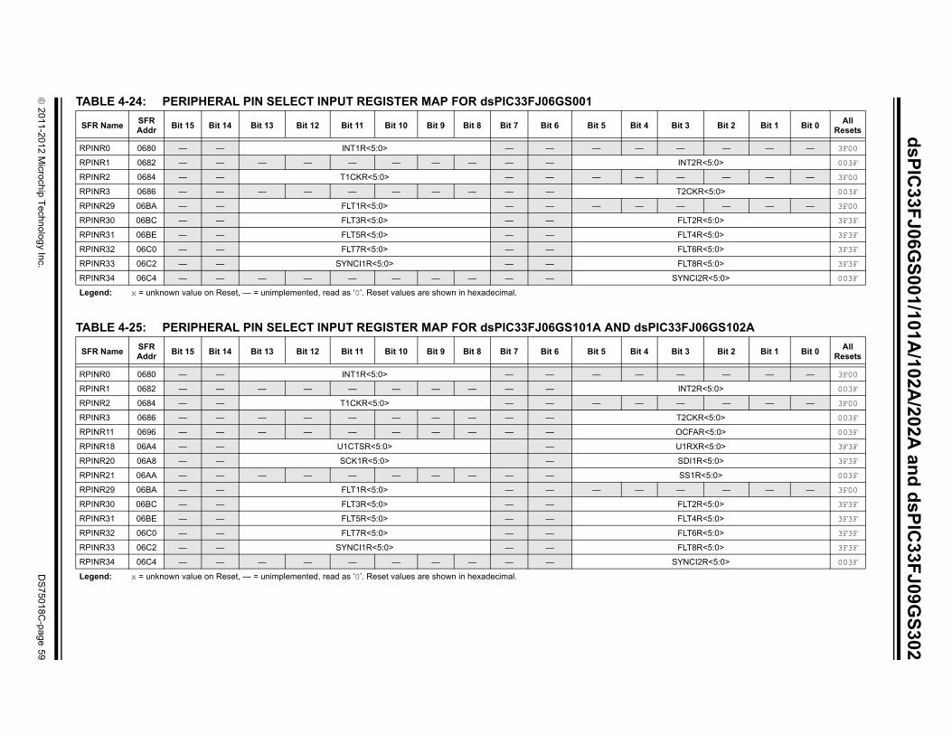
2011
-2012 Microchip T
echnology Inc.
DS
75018C
-page 59
dsP
IC33F
J06GS
001/101A/102A
/202A an
d d
sPIC
33FJ09G
S302
TA
TA 3FJ06GS102A
S Bit 3 Bit 2 Bit 1 Bit 0All
Resets
RP — — — — 3F00
RP INT2R<5:0> 003F
RP — — — — 3F00
RP T2CKR<5:0> 003F
RP — — — — 3F00
RP FLT2R<5:0> 3F3F
RP FLT4R<5:0> 3F3F
RP FLT6R<5:0> 3F3F
RP FLT8R<5:0> 3F3F
RP SYNCI2R<5:0> 003F
Le
S Bit 3 Bit 2 Bit 1 Bit 0All
Resets
RP — — — — 3F00
RP INT2R<5:0> 003F
RP — — — — 3F00
RP T2CKR<5:0> 003F
RP OCFAR<5:0> 003F
RP U1RXR<5:0> 3F3F
RP SDI1R<5:0> 3F3F
RP SS1R<5:0> 003F
RP — — — — 3F00
RP FLT2R<5:0> 3F3F
RP FLT4R<5:0> 3F3F
RP FLT6R<5:0> 3F3F
RP FLT8R<5:0> 3F3F
RP SYNCI2R<5:0> 003F
Le
BLE 4-24: PERIPHERAL PIN SELECT INPUT REGISTER MAP FOR dsPIC33FJ06GS001
BLE 4-25: PERIPHERAL PIN SELECT INPUT REGISTER MAP FOR dsPIC33FJ06GS101A AND dsPIC3
FR NameSFR Addr
Bit 15 Bit 14 Bit 13 Bit 12 Bit 11 Bit 10 Bit 9 Bit 8 Bit 7 Bit 6 Bit 5 Bit 4
INR0 0680 — — INT1R<5:0> — — — —
INR1 0682 — — — — — — — — — —
INR2 0684 — — T1CKR<5:0> — — — —
INR3 0686 — — — — — — — — — —
INR29 06BA — — FLT1R<5:0> — — — —
INR30 06BC — — FLT3R<5:0> — —
INR31 06BE — — FLT5R<5:0> — —
INR32 06C0 — — FLT7R<5:0> — —
INR33 06C2 — — SYNCI1R<5:0> — —
INR34 06C4 — — — — — — — — — —
gend: x = unknown value on Reset, — = unimplemented, read as ‘0’. Reset values are shown in hexadecimal.
FR NameSFR Addr
Bit 15 Bit 14 Bit 13 Bit 12 Bit 11 Bit 10 Bit 9 Bit 8 Bit 7 Bit 6 Bit 5 Bit 4
INR0 0680 — — INT1R<5:0> — — — —
INR1 0682 — — — — — — — — — —
INR2 0684 — — T1CKR<5:0> — — — —
INR3 0686 — — — — — — — — — —
INR11 0696 — — — — — — — — — —
INR18 06A4 — — U1CTSR<5:0> —
INR20 06A8 — — SCK1R<5:0> —
INR21 06AA — — — — — — — — — —
INR29 06BA — — FLT1R<5:0> — — — —
INR30 06BC — — FLT3R<5:0> — —
INR31 06BE — — FLT5R<5:0> — —
INR32 06C0 — — FLT7R<5:0> — —
INR33 06C2 — — SYNCI1R<5:0> — —
INR34 06C4 — — — — — — — — — —
gend: x = unknown value on Reset, — = unimplemented, read as ‘0’. Reset values are shown in hexadecimal.

dsP
IC33F
J06GS
001/101A/102A
/202A an
d d
sPIC
33FJ09G
S302
DS
75018C-page 60
2011-2012 M
icrochip Technolo
gy Inc.
IC33FJ09GS302
PIC33FJ06GS101A
Bit 3 Bit 2 Bit 1 Bit 0All
Resets
— — — — 3F00
INT2R<5:0> 003F
— — — — 3F00
T2CKR<5:0> 003F
IC1R<5:0> 003F
OCFAR<5:0> 003F
U1RXR<5:0> 3F3F
SDI1R<5:0> 3F3F
SS1R<5:0> 003F
— — — — 3F00
FLT2R<5:0> 3F3F
FLT4R<5:0> 3F3F
FLT6R<5:0> 3F3F
FLT8R<5:0> 3F3F
SYNCI2R<5:0> 003F
4 Bit 3 Bit 2 Bit 1 Bit 0All
Resets
RP0R<5:0> 0000
RP2R<5:0> 0000
RP4R<5:0> 0000
RP6R<5:0> 0000
RP32R<5:0> 0000
RP34R<5:0> 0000
TABLE 4-26: PERIPHERAL PIN SELECT INPUT REGISTER MAP FOR dsPIC33FJ06GS202A AND dsP
TABLE 4-27: PERIPHERAL PIN SELECT OUTPUT REGISTER MAP FOR dsPIC33FJ06GS001 AND ds
SFR NameSFR Addr
Bit 15 Bit 14 Bit 13 Bit 12 Bit 11 Bit 10 Bit 9 Bit 8 Bit 7 Bit 6 Bit 5 Bit 4
RPINR0 0680 — — INT1R<5:0> — — — —
RPINR1 0682 — — — — — — — — — —
RPINR2 0684 — — T1CKR<5:0> — — — —
RPINR3 0686 — — — — — — — — — —
RPINR7 068E — — — — — — — — — —
RPINR11 0696 — — — — — — — — — —
RPINR18 06A4 — — U1CTSR<5:0> — —
RPINR20 06A8 — — SCK1R<5:0> — —
RPINR21 06AA — — — — — — — — — —
RPINR29 06BA — — FLT1R<5:0> — — — —
RPINR30 06BC — — FLT3R<5:0> — —
RPINR31 06BE — — FLT5R<5:0> — —
RPINR32 06C0 — — FLT7R<5:0> — —
RPINR33 06C2 — — SYNCI1R<5:0> — —
RPINR34 06C4 — — — — — — — — — —
Legend: x = unknown value on Reset, — = unimplemented, read as ‘0’. Reset values are shown in hexadecimal.
File Name Addr Bit 15 Bit 14 Bit 13 Bit 12 Bit 11 Bit 10 Bit 9 Bit 8 Bit 7 Bit 6 Bit 5 Bit
RPOR0 06D0 — — RP1R<5:0> — —
RPOR1 06D2 — — RP3R<5:0> — —
RPOR2 06D4 — — RP5R<5:0> — —
RPOR3 06D6 — — RP7R<5:0> — —
RPOR16 06F0 — — RP33R<5:0> — —
RPOR17 06F2 — — RP35R<5:0> — —
Legend: x = unknown value on Reset, — = unimplemented, read as ‘0’. Reset values are shown in hexadecimal.

2011
-2012 Microchip T
echnology Inc.
DS
75018C
-page 61
dsP
IC33F
J06GS
001/101A/102A
/202A an
d d
sPIC
33FJ09G
S302
TA J06GS202A AND
Fi Bit 3 Bit 2 Bit 1 Bit 0All
Resets
RP RP0R<5:0> 0000
RP RP2R<5:0> 0000
RP RP4R<5:0> 0000
RP RP6R<5:0> 0000
RP RP8R<5:0> 0000
RP RP10R<5:0> 0000
RP RP12R<5:0> 0000
RP RP14R<5:0> 0000
RP RP32<5:0> 0000
RP RP34<5:0> 0000
Le
BLE 4-28: PERIPHERAL PIN SELECT OUTPUT REGISTER MAP FOR dsPIC33FJ06GS102A, dsPIC33FdsPIC33FJ09GS302
le Name Addr Bit 15 Bit 14 Bit 13 Bit 12 Bit 11 Bit 10 Bit 9 Bit 8 Bit 7 Bit 6 Bit 5 Bit 4
OR0 06D0 — — RP1R<5:0> — —
OR1 06D2 — — RP3R<5:0> — —
OR2 06D4 — — RP5R<5:0> — —
OR3 06D6 — — RP7R<5:0> — —
OR4 06D8 — — RP9R<5:0> — —
OR5 06DA — — RP11R<5:0> — —
OR6 06DC — — RP13R<5:0> — —
OR7 06DE — — RP15R<5:0> — —
OR16 06F0 — — RP33<5:0> — —
OR17 06F2 — — RP35<5:0> — —
gend: x = unknown value on Reset, — = unimplemented, read as ‘0’. Reset values are shown in hexadecimal.

dsP
IC33F
J06GS
001/101A/102A
/202A an
d d
sPIC
33FJ09G
S302
DS
75018C-page 62
2011-2012 M
icrochip Technolo
gy Inc.
3FJ09GS302
Bit 3 Bit 2 Bit 1 Bit 0All
Resets
TRISA3 TRISA2 TRISA1 TRISA0 001F
RA3 RA2 RA1 RA0 xxxx
LATA3 LATA2 LATA1 LATA0 0000
ODCA3 — — — 0000
Bit 3 Bit 2 Bit 1 Bit 0All
Resets
TRISB3 TRISB2 TRISB1 TRISB0 00FF
RB3 RB2 RB1 RB0 xxxx
LATB3 LATB2 LATB1 LATB0 0000
— — — — 0000
4 Bit 3 Bit 2 Bit 1 Bit 0All
Resets
B4 TRISB3 TRISB2 TRISB1 TRISB0 FFFF
4 RB3 RB2 RB1 RB0 xxxx
B4 LATB3 LATB2 LATB1 LATB0 0000
— — — — 0000
TABLE 4-29: PORTA REGISTER MAP
TABLE 4-30: PORTB REGISTER MAP FOR dsPIC33FJ06GS001 AND dsPIC33FJ06GS101A
TABLE 4-31: PORTB REGISTER MAP FOR dsPIC33FJ06GS102A, dsPIC33FJ06GS202A AND dsPIC3
SFR NameSFR Addr
Bit 15 Bit 14 Bit 13 Bit 12 Bit 11 Bit 10 Bit 9 Bit 8 Bit 7 Bit 6 Bit 5 Bit 4
TRISA 02C0 — — — — — — — — — — — TRISA4
PORTA 02C2 — — — — — — — — — — — RA4
LATA 02C4 — — — — — — — — — — — LATA4
ODCA 02C6 — — — — — — — — — — — ODCA4
Legend: x = unknown value on Reset, — = unimplemented, read as ‘0’. Reset values are shown in hexadecimal.
SFR NameSFR Addr
Bit 15 Bit 14 Bit 13 Bit 12 Bit 11 Bit 10 Bit 9 Bit 8 Bit 7 Bit 6 Bit 5 Bit 4
TRISB 02C8 — — — — — — — — TRISB7 TRISB6 TRISB5 TRISB4
PORTB 02CA — — — — — — — — RB7 RB6 RB5 RB4
LATB 02CC — — — — — — — — LATB7 LATB6 LATB5 LATB4
ODCB 02CE — — — — — — — — ODCB7 ODCB6 — —
Legend: x = unknown value on Reset, — = unimplemented, read as ‘0’. Reset values are shown in hexadecimal.
SFR Name
SFR Addr
Bit 15 Bit 14 Bit 13 Bit 12 Bit 11 Bit 10 Bit 9 Bit 8 Bit 7 Bit 6 Bit 5 Bit
TRISB 02C8 TRISB15 TRISB14 TRISB13 TRISB12 TRISB11 TRISB10 TRISB9 TRISB8 TRISB7 TRISB6 TRISB5 TRIS
PORTB 02CA RB15 RB14 RB13 RB12 RB11 RB10 RB9 RB8 RB7 RB6 RB5 RB
LATB 02CC LATB15 LATB14 LATB13 LATB12 LATB11 LATB10 LATB9 LATB8 LATB7 LATB6 LATB5 LAT
ODCB 02CE ODCB15 ODCB14 ODCB13 ODCB12 ODCB11 — — ODCB8 ODCB7 ODCB6 — —
Legend: x = unknown value on Reset, — = unimplemented, read as ‘0’. Reset values are shown in hexadecimal.

2011
-2012 Microchip T
echnology Inc.
DS
75018C
-page 63
dsP
IC33F
J06GS
001/101A/102A
/202A an
d d
sPIC
33FJ09G
S302
TA
TA
S it 3 Bit 2 Bit 1 Bit 0All
Resets
RC LEEP IDLE BOR POR xxxx(1)
OS CF — — OSWEN 0300(2)
CL PLLPRE<4:0> 3040
PL 0030
OS TUN<5:0> 0000
LF 0000
RE — — — — 0000
AC — — — — 0000
LeNo
Fi Bit 3 Bit 2 Bit 1 Bit 0All
Resets
NV NVMOP<3:0> 0000(1)
NV :0> 0000
LeNo t.
BLE 4-32: SYSTEM CONTROL REGISTER MAP
BLE 4-33: NVM REGISTER MAP
FR NameSFR Addr
Bit 15 Bit 14 Bit 13 Bit 12 Bit 11 Bit 10 Bit 9 Bit 8 Bit 7 Bit 6 Bit 5 Bit 4 B
ON 0740 TRAPR IOPUWR — — — — CM VREGS EXTR SWR SWDTEN WDTO S
CCON 0742 — COSC<2:0> — NOSC<2:0> CLKLOCK IOLOCK LOCK —
KDIV 0744 ROI DOZE<2:0> DOZEN FRCDIV<2:0> PLLPOST<1:0> —
LFBD 0746 — — — — — — — PLLDIV<8:0>
CTUN 0748 — — — — — — — — — —
SR 074C — LFSR<14:0>
FOCON 074E ROON — ROSSLP ROSEL RODIV<3:0> — — — —
LKCON 0750 ENAPLL APLLCK SELACLK — — APSTSCLR<2:0> ASRCSEL FRCSEL — —
gend: x = unknown value on Reset, — = unimplemented, read as ‘0’. Reset values are shown in hexadecimal.te 1: The RCON register Reset values are dependent on the type of Reset.
2: The OSCCON register Reset values are dependent on the FOSCx Configuration bits and on type of Reset.
le Name Addr Bit 15 Bit 14 Bit 13 Bit 12 Bit 11 Bit 10 Bit 9 Bit 8 Bit 7 Bit 6 Bit 5 Bit 4
MCON 0760 WR WREN WRERR — — — — — — ERASE — —
MKEY 0766 — — — — — — — — NVMKEY<7
gend: x = unknown value on Reset, — = unimplemented, read as ‘0’. Reset values are shown in hexadecimal.te 1: Reset value shown is for POR only. Value on other Reset states is dependent on the state of memory write or erase operations at the time of Rese

dsP
IC33F
J06GS
001/101A/102A
/202A an
d d
sPIC
33FJ09G
S302
DS
75018C-page 64
2011-2012 M
icrochip Technolo
gy Inc.
it 4 Bit 3 Bit 2 Bit 1 Bit 0All
Resets
— — — ADCMD 0000
— — — — 0000
REFOMD — — — 0000
— — — — 0000
— — — — 0000
it 4 Bit 3 Bit 2 Bit 1 Bit 0All
Resets
SPI1MD — — ADCMD 0000
— — — OC1MD 0000
REFOMD — — — 0000
— — — — 0000
it 4 Bit 3 Bit 2 Bit 1 Bit 0All
Resets
SPI1MD — — ADCMD 0000
— — — OC1MD 0000
REFOMD — — — 0000
— — — — 0000
TABLE 4-34: PMD REGISTER MAP FOR dsPIC33FJ06GS001
TABLE 4-35: PMD REGISTER MAP FOR dsPIC33FJ06GS101A
TABLE 4-36: PMD REGISTER MAP FOR dsPIC33FJ06GS102A
SFR Name
SFR Addr
Bit 15 Bit 14 Bit 13 Bit 12 Bit 11 Bit 10 Bit 9 Bit 8 Bit 7 Bit 6 Bit 5 B
PMD1 0770 — — — T2MD T1MD — PWMMD — I2C1MD — — —
PMD3 0774 — — — — — CMPMD — — — — — —
PMD4 0776 — — — — — — — — — — — —
PMD6 077A — — — — PWM4MD — — PWM1MD — — — —
PMD7 077C — — — — — — CMPMD2 CMPMD1 — — — —
Legend: x = unknown value on Reset, — = unimplemented, read as ‘0’. Reset values are shown in hexadecimal.
SFR Name
SFR Addr
Bit 15 Bit 14 Bit 13 Bit 12 Bit 11 Bit 10 Bit 9 Bit 8 Bit 7 Bit 6 Bit 5 B
PMD1 0770 — — — T2MD T1MD — PWMMD — I2C1MD — U1MD —
PMD2 0772 — — — — — — — — — — — —
PMD4 0776 — — — — — — — — — — — —
PMD6 077A — — — — PWM4MD — — PWM1MD — — — —
Legend: x = unknown value on Reset, — = unimplemented, read as ‘0’. Reset values are shown in hexadecimal.
SFR Name
SFR Addr
Bit 15 Bit 14 Bit 13 Bit 12 Bit 11 Bit 10 Bit 9 Bit 8 Bit 7 Bit 6 Bit 5 B
PMD1 0770 — — — T2MD T1MD — PWMMD — I2C1MD — U1MD —
PMD2 0772 — — — — — — — — — — — —
PMD4 0776 — — — — — — — — — — — —
PMD6 077A — — — — — — PWM2MD PWM1MD — — — —
Legend: x = unknown value on Reset, — = unimplemented, read as ‘0’. Reset values are shown in hexadecimal.

2011
-2012 Microchip T
echnology Inc.
DS
75018C
-page 65
dsP
IC33F
J06GS
001/101A/102A
/202A an
d d
sPIC
33FJ09G
S302
TA
TA
NBit 3 Bit 2 Bit 1 Bit 0
All Resets
PM SPI1MD — — ADCMD 0000
PM — — — OC1MD 0000
PM — — — — 0000
PM REFOMD — — — 0000
PM — — — — 0000
PM — — — — 0000
Le
NBit 3 Bit 2 Bit 1 Bit 0
All Resets
PM SPI1MD — — ADCMD 0000
PM — — — OC1MD 0000
PM — — — — 0000
PM REFOMD — — — 0000
PM — — — — 0000
PM — — — — 0000
PM — — CCSMD — 0000
Le
BLE 4-37: PMD REGISTER MAP FOR dsPIC33FJ06GS202A
BLE 4-38: PMD REGISTER MAP FOR dsPIC33FJ09GS302
SFR ame
SFR Addr
Bit 15 Bit 14 Bit 13 Bit 12 Bit 11 Bit 10 Bit 9 Bit 8 Bit 7 Bit 6 Bit 5 Bit 4
D1 0770 — — — T2MD T1MD — PWMMD — I2C1MD — U1MD —
D2 0772 — — — — — — — IC1MD — — — —
D3 0774 — — — — — CMPMD — — — — — —
D4 0776 — — — — — — — — — — — —
D6 077A — — — — — — PWM2MD PWM1MD — — — —
D7 077C — — — — — — CMP2MD CMP1MD — — — —
gend: x = unknown value on Reset, — = unimplemented, read as ‘0’. Reset values are shown in hexadecimal.
SFR ame
SFR Addr
Bit 15 Bit 14 Bit 13 Bit 12 Bit 11 Bit 10 Bit 9 Bit 8 Bit 7 Bit 6 Bit 5 Bit 4
D1 0770 — — — T2MD T1MD — PWMMD — I2C1MD — U1MD —
D2 0772 — — — — — — — IC1MD — — — —
D3 0774 — — — — — CMPMD — — — — — —
D4 0776 — — — — — — — — — — — —
D6 077A — — — — PWM4MD — PWM2MD PWM1MD — — — —
D7 077C — — — — — — CMP2MD CMP1MD — — — —
D8 077E — — — — — — — — — — — —
gend: x = unknown value on Reset, — = unimplemented, read as ‘0’. Reset values are shown in hexadecimal.

dsPIC33FJ06GS001/101A/102A/202A and dsPIC33FJ09GS302
4.3.1 SOFTWARE STACK
In addition to its use as a working register, the W15register in the devices is also used as a software StackPointer. The Stack Pointer always points to the firstavailable free word and grows from lower to higheraddresses. It predecrements for stack pops and post-increments for stack pushes, as shown in Figure 4-5.For a PC push during any CALL instruction, the MSb ofthe PC is zero-extended before the push, ensuring thatthe MSb is always clear.
The Stack Pointer Limit register (SPLIM) associatedwith the Stack Pointer sets an upper address boundaryfor the stack. SPLIM is uninitialized at Reset. As is thecase for the Stack Pointer, SPLIM<0> is forced to ‘0’because all stack operations must be word-aligned.
Whenever an EA is generated using W15 as a sourceor destination pointer, the resulting address iscompared with the value in SPLIM. If the contents ofthe Stack Pointer (W15) and the SPLIM register areequal and a push operation is performed, a stack errortrap will not occur. The stack error trap will occur on asubsequent push operation. For example, to cause astack error trap when the stack grows beyond address0x1000 in RAM, initialize the SPLIM with the value0x0FFE.
Similarly, a Stack Pointer underflow (stack error) trap isgenerated when the Stack Pointer address is found tobe less than 0x0800. This prevents the stack frominterfering with the Special Function Register (SFR)space.
A write to the SPLIM register should not be immediatelyfollowed by an indirect read operation using W15.
FIGURE 4-5: CALL STACK FRAME
4.4 Instruction Addressing Modes
The addressing modes shown in Table 4-39 form thebasis of the addressing modes optimized to support thespecific features of individual instructions. Theaddressing modes provided in the MAC class ofinstructions differ from those in the other instructiontypes.
4.4.1 FILE REGISTER INSTRUCTIONS
Most file register instructions use a 13-bit address field(f) to directly address data present in the first 8192bytes of data memory (Near Data Space). Most fileregister instructions employ a working register, W0,which is denoted as WREG in these instructions. Thedestination is typically either the same file register orWREG (with the exception of the MUL instruction),which writes the result to a register or register pair. TheMOV instruction allows additional flexibility and canaccess the entire data space.
4.4.2 MCU INSTRUCTIONS
The three-operand MCU instructions are of the form:
Operand 3 = Operand 1 <function> Operand 2
where Operand 1 is always a working register (that is,the addressing mode can only be register direct), whichis referred to as Wb. Operand 2 can be a W register,fetched from data memory, or a 5-bit literal. The resultlocation can be either a W register or a data memorylocation. The following addressing modes aresupported by MCU instructions:
• Register Direct
• Register Indirect
• Register Indirect Post-Modified
• Register Indirect Pre-Modified
• 5-Bit or 10-Bit Literal
Note: A PC push during exception processingconcatenates the SRL register to the MSbof the PC prior to the push.
<Free Word>
PC<15:0>
000000000
015
W15 (before CALL)
W15 (after CALL)
Sta
ck G
row
s To
war
dH
ighe
r A
ddr
ess
0x0000
PC<22:16>
POP : [--W15]PUSH : [W15++]
Note: Not all instructions support all of theaddressing modes shown above.Individual instructions can supportdifferent subsets of these addressingmodes.
DS75018C-page 66 2011-2012 Microchip Technology Inc.

dsPIC33FJ06GS001/101A/102A/202A and dsPIC33FJ09GS302
TABLE 4-39: FUNDAMENTAL ADDRESSING MODES SUPPORTED
4.4.3 MOVE AND ACCUMULATOR INSTRUCTIONS
Move instructions and the DSP accumulator class ofinstructions provide a greater degree of addressingflexibility than other instructions. In addition to theaddressing modes supported by most MCUinstructions, move and accumulator instructions alsosupport Register Indirect with Register OffsetAddressing mode, also referred to as Register Indexedmode.
In summary, the following addressing modes aresupported by move and accumulator instructions:
• Register Direct
• Register Indirect
• Register Indirect Post-modified
• Register Indirect Pre-modified
• Register Indirect with Register Offset (Indexed)
• Register Indirect with Literal Offset
• 8-Bit Literal
• 16-Bit Literal
4.4.4 MAC INSTRUCTIONS
The dual source operand DSP instructions (CLR, ED,EDAC, MAC, MPY, MPY.N, MOVSAC and MSC), also referredto as MAC instructions, use a simplified set of addressingmodes to allow the user application to effectivelymanipulate the data pointers through register indirecttables.
The two-source operand prefetch registers must bemembers of the set {W8, W9, W10, W11}. For datareads, W8 and W9 are always directed to the X RAGU,and W10 and W11 are always directed to the Y AGU.The Effective Addresses generated (before and aftermodification) must, therefore, be valid addresses withinX data space for W8 and W9 and Y data space for W10and W11.
In summary, the following addressing modes aresupported by the MAC class of instructions:
• Register Indirect
• Register Indirect Post-modified by 2
• Register Indirect Post-modified by 4
• Register Indirect Post-modified by 6
• Register Indirect with Register Offset (Indexed)
4.4.5 OTHER INSTRUCTIONS
Besides the addressing modes outlined previously, someinstructions use literal constants of various sizes. Forexample, BRA (branch) instructions use 16-bit signedliterals to specify the branch destination directly, whereasthe DISI instruction uses a 14-bit unsigned literal field. Insome instructions, such as ADD Acc, the source of anoperand or result is implied by the opcode itself. Certainoperations, such as NOP, do not have any operands.
Addressing Mode Description
File Register Direct The address of the File register is specified explicitly.
Register Direct The contents of a register are accessed directly.
Register Indirect The contents of Wn forms the Effective Address (EA).
Register Indirect Post-Modified The contents of Wn forms the EA. Wn is post-modified (incremented or decremented) by a constant value.
Register Indirect Pre-Modified Wn is pre-modified (incremented or decremented) by a signed constant value to form the EA.
Register Indirect with Register Offset (Register Indexed)
The sum of Wn and Wb forms the EA.
Register Indirect with Literal Offset The sum of Wn and a literal forms the EA.
Note: For the MOV instructions, the addressingmode specified in the instruction can differfor the source and destination EA.However, the 4-bit Wb (register offset)field is shared by both source anddestination (but typically only used byone).
Note: Not all instructions support all theaddressing modes given above. Individualinstructions may support different subsetsof these addressing modes.
Note: Register Indirect with Register OffsetAddressing mode is available only for W9(in X space) and W11 (in Y space).
2011-2012 Microchip Technology Inc. DS75018C-page 67

dsPIC33FJ06GS001/101A/102A/202A and dsPIC33FJ09GS302
4.5 Modulo Addressing
Modulo Addressing mode is a method used to providean automated means to support circular data buffersusing hardware. The objective is to remove the needfor software to perform data address boundary checkswhen executing tightly looped code, as is typical inmany DSP algorithms.
Modulo Addressing can operate in either data or programspace (since the data pointer mechanism is essentiallythe same for both). One circular buffer can be supportedin each of the X (which also provides the pointers intoprogram space) and Y data spaces. Modulo Addressingcan operate on any W register pointer. However, it is notadvisable to use W14 or W15 for Modulo Addressingsince these two registers are used as the Stack FramePointer and Stack Pointer, respectively.
In general, any particular circular buffer can beconfigured to operate in only one direction as there arecertain restrictions on the buffer start address (forincrementing buffers), or end address (fordecrementing buffers), based upon the direction of thebuffer.
The only exception to the usage restrictions is forbuffers that have a power-of-two length. As thesebuffers satisfy the start and end address criteria, theycan operate in a bidirectional mode (that is, addressboundary checks are performed on both the lower andupper address boundaries).
4.5.1 START AND END ADDRESS
The Modulo Addressing scheme requires that astarting and ending address be specified and loadedinto the 16-bit Modulo Buffer Address registers:XMODSRT, XMODEND, YMODSRT and YMODEND(see Table 4-1).
The length of a circular buffer is not directly specified. Itis determined by the difference between thecorresponding start and end addresses. The maximumpossible length of the circular buffer is 32K words(64 Kbytes).
4.5.2 W ADDRESS REGISTER SELECTION
The Modulo and Bit-Reversed Addressing Controlregister, MODCON<15:0>, contains enable flags aswell as a W register field to specify the W Addressregisters. The XWM and YWM fields select theregisters that will operate with Modulo Addressing:
• If XWM = 15, X RAGU and X WAGU Modulo Addressing is disabled
• If YWM = 15, Y AGU Modulo Addressing is disabled
The X Address Space Pointer W register (XWM), towhich Modulo Addressing is to be applied, is stored inMODCON<3:0> (see Table 4-1). Modulo Addressing isenabled for X data space when XWM is set to any valueother than ‘15’ and the XMODEN bit is set atMODCON<15>.
The Y Address Space Pointer W register (YWM) towhich Modulo Addressing is to be applied is stored inMODCON<7:4>. Modulo Addressing is enabled for Ydata space when YWM is set to any value other than‘15’ and the YMODEN bit is set at MODCON<14>.
FIGURE 4-6: MODULO ADDRESSING OPERATION EXAMPLE
Note: Y space Modulo Addressing EAcalculations assume word-sized data(LSb of every EA is always clear).
0x1100
0x1163
Start Addr = 0x1100End Addr = 0x1163Length = 32 words
ByteAddress
MOV #0x1100, W0MOV W0, XMODSRT ;set modulo start addressMOV #0x1163, W0MOV W0, MODEND ;set modulo end addressMOV #0x8001, W0MOV W0, MODCON ;enable W1, X AGU for modulo
MOV #0x0000, W0 ;W0 holds buffer fill value
MOV #0x1110, W1 ;point W1 to buffer
DO AGAIN, #0x31 ;fill the 50 buffer locationsMOV W0, [W1++] ;fill the next locationAGAIN: INC W0, W0 ;increment the fill value
DS75018C-page 68 2011-2012 Microchip Technology Inc.

dsPIC33FJ06GS001/101A/102A/202A and dsPIC33FJ09GS302
4.5.3 MODULO ADDRESSING APPLICABILITY
Modulo Addressing can be applied to the EffectiveAddress (EA) calculation associated with any Wregister. Address boundaries check for addressesequal to:
• Upper boundary addresses for incrementing buffers
• Lower boundary addresses for decrementing buffers
It is important to realize that the address boundariescheck for addresses less than or greater than the upper(for incrementing buffers) and lower (for decrementingbuffers) boundary addresses (not just equal to).Address changes can, therefore, jump beyondboundaries and still be adjusted correctly.
4.6 Bit-Reversed Addressing
Bit-Reversed Addressing mode is intended to simplifydata re-ordering for radix-2 FFT algorithms. It issupported by the X AGU for data writes only.
The modifier, which can be a constant value or registercontents, is regarded as having its bit order reversed. Theaddress source and destination are kept in normal order.Thus, the only operand requiring reversal is the modifier.
4.6.1 BIT-REVERSED ADDRESSING IMPLEMENTATION
Bit-Reversed Addressing mode is enabled when all ofthese conditions are met:
• BWMx bits (W register selection) in the MODCON register are any value other than ‘15’ (the stack cannot be accessed using Bit-Reversed Addressing)
• BREN bit is set in the XBREV register
• Addressing mode used is Register Indirect with Pre-increment or Post-increment
If the length of a bit-reversed buffer is M = 2N bytes,the last ‘N’ bits of the data buffer start address mustbe zeros.
XB<14:0> is the Bit-Reversed Address modifier, or‘pivot point,’ which is typically a constant. In the case ofan FFT computation, its value is equal to half of the FFTdata buffer size.
When enabled, Bit-Reversed Addressing is executedonly for Register Indirect with Pre-Increment or Post-Increment Addressing and word-sized data writes. Itwill not function for any other addressing mode or forbyte-sized data, and normal addresses are generatedinstead. When Bit-Reversed Addressing is active, theW Address Pointer is always added to the addressmodifier (XB), and the offset associated with the Regis-ter Indirect Addressing mode is ignored. In addition, asword-sized data is a requirement, the LSb of the EA isignored (and always clear).
If Bit-Reversed Addressing has already been enabledby setting the BREN (XBREV<15>) bit, a write to theXBREV register should not be immediately followed byan indirect read operation using the W register that hasbeen designated as the Bit-Reversed Pointer.
Note: The modulo corrected Effective Address iswritten back to the register only when Pre-Modify or Post-Modify Addressing mode isused to compute the Effective Address.When an address offset (such as[W7 + W2]) is used, Modulo Addressingcorrection is performed but the contents ofthe register remain unchanged.
Note: All bit-reversed EA calculations assumeword-sized data (LSb of every EA isalways clear). The XB value is scaledaccordingly to generate compatible (byte)addresses.
Note: Modulo Addressing and Bit-ReversedAddressing should not be enabledtogether. If an application attempts to doso, Bit-Reversed Addressing will assumepriority when active for the X WAGU and XWAGU; Modulo Addressing will be dis-abled. However, Modulo Addressing willcontinue to function in the X RAGU.
2011-2012 Microchip Technology Inc. DS75018C-page 69

dsPIC33FJ06GS001/101A/102A/202A and dsPIC33FJ09GS302
FIGURE 4-7: BIT-REVERSED ADDRESS EXAMPLE
TABLE 4-40: BIT-REVERSED ADDRESS SEQUENCE (16-ENTRY)
Normal Address Bit-Reversed Address
A3 A2 A1 A0 Decimal A3 A2 A1 A0 Decimal
0 0 0 0 0 0 0 0 0 0
0 0 0 1 1 1 0 0 0 8
0 0 1 0 2 0 1 0 0 4
0 0 1 1 3 1 1 0 0 12
0 1 0 0 4 0 0 1 0 2
0 1 0 1 5 1 0 1 0 10
0 1 1 0 6 0 1 1 0 6
0 1 1 1 7 1 1 1 0 14
1 0 0 0 8 0 0 0 1 1
1 0 0 1 9 1 0 0 1 9
1 0 1 0 10 0 1 0 1 5
1 0 1 1 11 1 1 0 1 13
1 1 0 0 12 0 0 1 1 3
1 1 0 1 13 1 0 1 1 11
1 1 1 0 14 0 1 1 1 7
1 1 1 1 15 1 1 1 1 15
b3 b2 b1 0
b2 b3 b4 0
Bit Locations Swapped Left-to-RightAround Center of Binary Value
Bit-Reversed Address
XB = 0x0008 for a 16-Word Bit-Reversed Buffer
b7 b6 b5 b1
b7 b6 b5 b4b11 b10 b9 b8
b11 b10 b9 b8
b15 b14 b13 b12
b15 b14 b13 b12
Sequential Address
Pivot Point
DS75018C-page 70 2011-2012 Microchip Technology Inc.

dsPIC33FJ06GS001/101A/102A/202A and dsPIC33FJ09GS302
4.7 Interfacing Program and Data Memory Spaces
The device architecture uses a 24-bit wide program spaceand a 16-bit wide data space. The architecture is also amodified Harvard scheme, meaning that data can also bepresent in the program space. To use this data success-fully, it must be accessed in a way that preserves thealignment of information in both spaces.
Aside from normal execution, the device architectureprovides two methods by which program space can beaccessed during operation:
• Using table instructions to access individual bytes or words anywhere in the program space
• Remapping a portion of the program space into the data space (Program Space Visibility)
Table instructions allow an application to read or writeto small areas of the program memory. This capabilitymakes the method ideal for accessing data tables thatneed to be updated periodically. It also allows accessto all bytes of the program word. The remappingmethod allows an application to access a large block ofdata on a read-only basis, which is ideal for look upsfrom a large table of static data. The application canonly access the least significant word of the programword.
4.7.1 ADDRESSING PROGRAM SPACE
Since the address ranges for the data and programspaces are 16 and 24 bits, respectively, a method isneeded to create a 23-bit or 24-bit program addressfrom 16-bit data registers. The solution depends on theinterface method to be used.
For table operations, the 8-bit Table Page register(TBLPAG) is used to define a 32K word region withinthe program space. This is concatenated with a 16-bitEA to arrive at a full 24-bit program space address. Inthis format, the Most Significant bit of TBLPAG is usedto determine if the operation occurs in the user memory(TBLPAG<7> = 0) or the configuration memory(TBLPAG<7> = 1).
For remapping operations, the 8-bit Program SpaceVisibility Register (PSVPAG) is used to define a16K word page in the program space. When the MostSignificant bit of the EA is ‘1’, PSVPAG is concatenatedwith the lower 15 bits of the EA to form a 23-bit programspace address. Unlike table operations, this limitsremapping operations strictly to the user memory area.
Table 4-41 and Figure 4-8 show how the program EA iscreated for table operations and remapping accessesfrom the data EA. Here, P<23:0> refers to a programspace word, and D<15:0> refers to a data space word.
TABLE 4-41: PROGRAM SPACE ADDRESS CONSTRUCTION
Access TypeAccessSpace
Program Space Address
<23> <22:16> <15> <14:1> <0>
Instruction Access(Code Execution)
User 0 PC<22:1> 0
0xx xxxx xxxx xxxx xxxx xxx0
TBLRD/TBLWT(Byte/Word Read/Write)
User TBLPAG<7:0> Data EA<15:0>
0xxx xxxx xxxx xxxx xxxx xxxx
Configuration TBLPAG<7:0> Data EA<15:0>
1xxx xxxx xxxx xxxx xxxx xxxx
Program Space Visibility(Block Remap/Read)
User 0 PSVPAG<7:0> Data EA<14:0>(1)
0 xxxx xxxx xxx xxxx xxxx xxxx
Note 1: Data EA<15> is always ‘1’ in this case, but is not used in calculating the program space address. Bit 15 of the address is PSVPAG<0>.
2011-2012 Microchip Technology Inc. DS75018C-page 71

dsPIC33FJ06GS001/101A/102A/202A and dsPIC33FJ09GS302
FIGURE 4-8: DATA ACCESS FROM PROGRAM SPACE ADDRESS GENERATION
0Program Counter
23 bits
1
PSVPAG
8 bits
EA
15 bits
Program Counter(1)
Select
TBLPAG
8 bits
EA
16 bits
Byte Select
0
0
1/0
User/Configuration
Table Operations(2)
Program Space Visibility(1)
Space Select
24 bits
23 bits
(Remapping)
1/0
0
Note 1: The Least Significant bit (LSb) of program space addresses is always fixed as ‘0’ to maintain wordalignment of data in the program and data spaces.
2: Table operations are not required to be word-aligned. Table read operations are permitted in theconfiguration memory space.
DS75018C-page 72 2011-2012 Microchip Technology Inc.

dsPIC33FJ06GS001/101A/102A/202A and dsPIC33FJ09GS302
4.7.2 DATA ACCESS FROM PROGRAM MEMORY USING TABLE INSTRUCTIONS
The TBLRDL and TBLWTL instructions offer a directmethod of reading or writing the lower word of anyaddress within the program space without goingthrough data space. The TBLRDH and TBLWTHinstructions are the only method to read or write theupper 8 bits of a program space word as data.
The PC is incremented by two for each successive24-bit program word. This allows program memoryaddresses to directly map to data space addresses.Program memory can thus be regarded as two 16-bitwide word address spaces, residing side by side, eachwith the same address range. TBLRDL and TBLWTLaccess the space that contains the least significantdata word. TBLRDH and TBLWTH access the space thatcontains the upper data byte.
Two table instructions are provided to move byte orword-sized (16-bit) data to and from program space.Both function as either byte or word operations.
• TBLRDL (Table Read Low):
- In Word mode, this instruction maps the lower word of the program space location (P<15:0>) to a data address (D<15:0>)
- In Byte mode, either the upper or lower byte of the lower program word is mapped to the lower byte of a data address. The upper byte is selected when byte select is ‘1’; the lower byte is selected when it is ‘0’.
• TBLRDH (Table Read High):
- In Word mode, this instruction maps the entire upper word of a program address (P<23:16>) to a data address. Note that D<15:8>, the ‘phantom byte’, will always be ‘0’.
- In Byte mode, this instruction maps the upper or lower byte of the program word to D<7:0> of the data address, in the TBLRDL instruction. The data is always ‘0’ when the upper ‘phantom’ byte is selected (Byte Select = 1).
Similarly, two table instructions, TBLWTH and TBLWTL,are used to write individual bytes or words to a programspace address. The details of their operation areexplained in Section 5.0 “Flash Program Memory”.
For all table operations, the area of program memoryspace to be accessed is determined by the Table Pageregister (TBLPAG). TBLPAG covers the entire programmemory space of the device, including user andconfiguration spaces. When TBLPAG<7> = 0, the tablepage is located in the user memory space. WhenTBLPAG<7> = 1, the page is located in configurationspace.
FIGURE 4-9: ACCESSING PROGRAM MEMORY WITH TABLE INSTRUCTIONS
081623
00000000
00000000
00000000
00000000
‘Phantom’ Byte
TBLRDH.B (Wn<0> = 0)
TBLRDL.W
TBLRDL.B (Wn<0> = 1)
TBLRDL.B (Wn<0> = 0)
23 15 0
TBLPAG02
0x000000
0x800000
0x020000
0x030000
Program Space
The address for the table operation is determined by the data EAwithin the page defined by the TBLPAG register. Only read operations are shown; write operations are also valid inthe user memory area.
2011-2012 Microchip Technology Inc. DS75018C-page 73

dsPIC33FJ06GS001/101A/102A/202A and dsPIC33FJ09GS302
4.7.3 READING DATA FROM PROGRAM MEMORY USING PROGRAM SPACE VISIBILITY
The upper 32 Kbytes of data space may optionally bemapped into any 16K word page of the program space.This option provides transparent access to storedconstant data from the data space without the need touse special instructions (such as TBLRDL or TBLRDH).
Program space access through the data space occursif the Most Significant bit of the data space EA is ‘1’ andprogram space visibility is enabled by setting the PSVbit in the Core Control register (CORCON<2>). Thelocation of the program memory space to be mappedinto the data space is determined by the ProgramSpace Visibility Page register (PSVPAG). This 8-bitregister defines any one of 256 possible pages of16K words in program space. In effect, PSVPAGfunctions as the upper 8 bits of the program memoryaddress, with the 15 bits of the EA functioning as thelower bits. By incrementing the PC by 2 for eachprogram memory word, the lower 15 bits of data spaceaddresses directly map to the lower 15 bits in thecorresponding program space addresses.
Data reads to this area add a cycle to the instructionbeing executed, since two program memory fetchesare required.
Although each data space address 0x8000 and highermaps directly into a corresponding program memoryaddress (see Figure 4-10), only the lower 16 bits of the24-bit program word are used to contain the data. Theupper 8 bits of any program space location used asdata should be programmed with ‘1111 1111’ or‘0000 0000’ to force a NOP. This prevents possibleissues should the area of code ever be accidentallyexecuted.
For operations that use PSV and are executed outsidea REPEAT loop, the MOV and MOV.D instructions requireone instruction cycle in addition to the specifiedexecution time. All other instructions require twoinstruction cycles in addition to the specified executiontime.
For operations that use PSV, and are executed insidea REPEAT loop, these instances require two instructioncycles in addition to the specified execution time of theinstruction:
• Execution in the first iteration
• Execution in the last iteration
• Execution prior to exiting the loop due to an interrupt
• Execution upon re-entering the loop after an interrupt is serviced
Any other iteration of the REPEAT loop will allow theinstruction using PSV to access data, to execute in asingle cycle.
FIGURE 4-10: PROGRAM SPACE VISIBILITY OPERATION
Note: PSV access is temporarily disabled duringtable reads/writes.
23 15 0PSVPAGData SpaceProgram Space
0x0000
0x8000
0xFFFF
020x000000
0x800000
0x010000
0x018000
When CORCON<2> = 1 and EA<15> = 1:
The data in the page designated by PSVPAG is mapped into the upper half of the data memory space...
Data EA<14:0>
...while the lower 15 bits of the EA specify an exact address within the PSV area. This corresponds exactly to the same lower 15 bits of the actual program space address.
PSV Area
DS75018C-page 74 2011-2012 Microchip Technology Inc.

dsPIC33FJ06GS001/101A/102A/202A and dsPIC33FJ09GS302
5.0 FLASH PROGRAM MEMORY
These devices contain internal Flash program memory forstoring and executing application code. The memory isreadable, writable and erasable during normal operationover the entire VDD range.
Flash memory can be programmed in two ways:
• In-Circuit Serial Programming™ (ICSP™) programming capability
• Run-Time Self-Programming (RTSP)
ICSP allows a dsPIC33FJ06GS001/101A/102A/202Aand dsPIC33FJ09GS302 device to be seriallyprogrammed while in the end application circuit. This isdone with two lines for programming clock andprogramming data (one of the alternate programming
pin pairs: PGECx/PGEDx), and three other lines forpower (VDD), ground (VSS) and Master Clear (MCLR).This allows customers to manufacture boards withunprogrammed devices and then program the digitalsignal controller just before shipping the product. Thisalso allows the most recent firmware or a customfirmware to be programmed.
RTSP is accomplished using TBLRD (table read) andTBLWT (table write) instructions. With RTSP, the userapplication can write a single program memory word ata time, and erase program memory in blocks or ‘pages’of 512 instructions (1536 bytes) at a time.
5.1 Table Instructions and Flash Programming
Regardless of the method used, all programming ofFlash memory is done with the table read and tablewrite instructions. These allow direct read and writeaccess to the program memory space from the datamemory while the device is in normal operating mode.The 24-bit target address in the program memory isformed using bits<7:0> of the TBLPAG register and theEffective Address (EA) from a W register specified inthe table instruction, as shown in Figure 5-1.
The TBLRDL and the TBLWTL instructions are used toread or write to bits<15:0> of program memory.TBLRDL and TBLWTL can access program memory inboth Word and Byte modes.
The TBLRDH and TBLWTH instructions are used to reador write to bits<23:16> of program memory. TBLRDHand TBLWTH can also access program memory in Wordor Byte mode.
FIGURE 5-1: ADDRESSING FOR TABLE REGISTERS
Note 1: This data sheet summarizes the featuresof the dsPIC33FJ06GS001/101A/102A/202A and dsPIC33FJ09GS302families of devices. It is not intendedto be a comprehensive referencesource. To complement the informa-tion in this data sheet, refer toSection 5. “Flash Programming”(DS70191) in the “dsPIC33F/PIC24HFamily Reference Manual”, which isavailable from the Microchip web site(www.microchip.com).
2: Some registers and associated bitsdescribed in this section may not beavailable on all devices. Refer toSection 4.0 “Memory Organization” inthis data sheet for device-specific registerand bit information.
0Program Counter
24 bits
Program Counter
TBLPAG Reg
8 bits
Working Reg EA
16 bits
Byte24-bit EA
0
1/0
Select
UsingTable Instruction
Using
User/ConfigurationSpace Select
2011-2012 Microchip Technology Inc. DS75018C-page 75

dsPIC33FJ06GS001/101A/102A/202A and dsPIC33FJ09GS302
5.2 RTSP Operation
The dsPIC33FJ06GS001/101A/102A/202A anddsPIC33FJ09GS302 Flash program memory array isorganized into rows of 64 instructions or 192 bytes. RTSPallows the user application to erase a page of mem-ory, which consists of eight rows (512 instructions) ata time, and to program one row or one word at a time.Table 25-12 shows typical erase and programming times.The 8-row erase pages and single row write rows areedge-aligned from the beginning of program memory, onboundaries of 1536 bytes and 192 bytes, respectively.
The program memory implements holding buffers thatcan contain 64 instructions of programming data. Priorto the actual programming operation, the write datamust be loaded into the buffers sequentially. Theinstruction words loaded must always be from a groupof 64 boundary.
The basic sequence for RTSP programming is to set upa Table Pointer, then do a series of TBLWT instructionsto load the buffers. Programming is performed bysetting the control bits in the NVMCON register. A totalof 64 TBLWTL and TBLWTH instructions are requiredto load the instructions.
All of the table write operations are single-word writes(two instruction cycles) because only the buffers are writ-ten. A programming cycle is required for programmingeach row.
5.3 Programming Operations
A complete programming sequence is necessary forprogramming or erasing the internal Flash in RTSPmode. The processor stalls (waits) until theprogramming operation is finished.
The programming time depends on the FRC accuracy(see Table 25-19) and the value of the FRC OscillatorTuning register (see Register 8-4). Use the followingformula to calculate the minimum and maximum valuesfor the Row Write Time, Page Erase Time and WordWrite Cycle Time parameters (see Table 25-12).
EQUATION 5-1: PROGRAMMING TIME
For example, if the device is operating at +125°C, theFRC accuracy will be ±5%. If the TUN<5:0> bits (seeRegister 8-4) are set to ‘b111111, the minimum rowwrite time is equal to Equation 5-2.
EQUATION 5-2: MINIMUM PAGE ERASE TIME
The maximum row write time is equal to Equation 5-3.
EQUATION 5-3: MAXIMUM PAGE ERASE TIME
Setting the WR bit (NVMCON<15>) starts the opera-tion, and the WR bit is automatically cleared when theoperation is finished.
5.4 Control Registers
Two SFRs are used to read and write the programFlash memory: NVMCON and NVMKEY.
The NVMCON register (Register 5-1) controls whichblocks are to be erased, which memory type is to beprogrammed and the start of the programming cycle.
NVMKEY is a write-only register that is used for writeprotection. To start a programming or erase sequence,the user application must consecutively write 0x55 and0xAA to the NVMKEY register. Refer to Section 5.3“Programming Operations” for further details.
T7.37 MHz FRC Accuracy % FRC Tuning %--------------------------------------------------------------------------------------------------------------------------
TRW168517 Cycles
7.37 MHz 1 0.05+ 1 0.00375– ---------------------------------------------------------------------------------------------- 21.85ms==
TRW168517 Cycles
7.37 MHz 1 0.05– 1 0.00375– ---------------------------------------------------------------------------------------------- 24.16ms==
DS75018C-page 76 2011-2012 Microchip Technology Inc.

dsPIC33FJ06GS001/101A/102A/202A and dsPIC33FJ09GS302
5.5 Flash Memory Control Registers
REGISTER 5-1: NVMCON: FLASH MEMORY CONTROL REGISTER
R/SO-0 R/W-0 R/W-0 U-0 U-0 U-0 U-0 U-0
WR(1) WREN(1) WRERR(1) — — — — —
bit 15 bit 8
U-0 R/W-0 U-0 U-0 R/W-0 R/W-0 R/W-0 R/W-0
— ERASE(1) — — NVMOP<3:0>(1,2)
bit 7 bit 0
Legend: SO = Settable Only bit
R = Readable bit W = Writable bit U = Unimplemented bit, read as ‘0’
-n = Value at POR ‘1’ = Bit is set ‘0’ = Bit is cleared x = Bit is unknown
bit 15 WR: Write Control bit(1)
1 = Initiates a Flash memory program or erase operation. The operation is self-timed and the bit iscleared by hardware once operation is complete. This bit can only be set (not cleared) in software.
0 = Program or erase operation is complete and inactive
bit 14 WREN: Write Enable bit(1)
1 = Enables Flash program/erase operations0 = Inhibits Flash program/erase operations
bit 13 WRERR: Write Sequence Error Flag bit(1)
1 = An improper program or erase sequence attempt or termination has occurred (bit is setautomatically on any set attempt of the WR bit)
0 = The program or erase operation completed normally
bit 12-7 Unimplemented: Read as ‘0’
bit 6 ERASE: Erase/Program Enable bit(1)
1 = Performs the erase operation specified by NVMOP<3:0> on the next WR command0 = Performs the program operation specified by NVMOP<3:0> on the next WR command
bit 5-4 Unimplemented: Read as ‘0’
bit 3-0 NVMOP<3:0>: NVM Operation Select bits(1,2)
If ERASE = 1:1111 = No operation1101 = Erase general segment0011 = No operation0010 = Memory page erase operation0001 = Reserved0000 = Reserved
If ERASE = 0:1111 = No operation1101 = No operation0011 = Memory word program operation0010 = No operation0001 = Reserved0000 = Reserved
Note 1: These bits can only be reset on a Power-on Reset (POR).
2: All other combinations of NVMOP<3:0> are unimplemented.
2011-2012 Microchip Technology Inc. DS75018C-page 77

dsPIC33FJ06GS001/101A/102A/202A and dsPIC33FJ09GS302
REGISTER 5-2: NVMKEY: NONVOLATILE MEMORY KEY REGISTER
U-0 U-0 U-0 U-0 U-0 U-0 U-0 U-0
— — — — — — — —
bit 15 bit 8
W-0 W-0 W-0 W-0 W-0 W-0 W-0 W-0
NVMKEY<7:0>
bit 7 bit 0
Legend:
R = Readable bit W = Writable bit U = Unimplemented bit, read as ‘0’
-n = Value at POR ‘1’ = Bit is set ‘0’ = Bit is cleared x = Bit is unknown
bit 15-8 Unimplemented: Read as ‘0’
bit 7-0 NVMKEY<7:0>: Key Register bits (write-only)
DS75018C-page 78 2011-2012 Microchip Technology Inc.

dsPIC33FJ06GS001/101A/102A/202A and dsPIC33FJ09GS302
6.0 RESETS
The Reset module combines all Reset sources andcontrols the device Master Reset Signal, SYSRST. Thefollowing is a list of device Reset sources:
• POR: Power-on Reset
• BOR: Brown-out Reset
• MCLR: Master Clear Pin Reset
• SWR: Software RESET Instruction
• WDTO: Watchdog Timer Reset
• CM: Configuration Mismatch Reset
• TRAPR: Trap Conflict Reset
• IOPUWR: Illegal Condition Device Reset
- Illegal Opcode Reset
- Uninitialized W Register Reset
- Security Reset
A simplified block diagram of the Reset module isshown in Figure 6-1.
Any active source of Reset will make the SYSRSTsignal active. On system Reset, some of the registersassociated with the CPU and peripherals are forced toa known Reset state, and some are unaffected.
All types of device Reset sets a corresponding statusbit in the RCON register to indicate the type of Reset(see Register 6-1).
A POR clears all the bits (except for the POR(RCON<0> bit) that are set. The user application canset or clear any bit, at any time, during code execution.The RCON bits only serve as status bits. Setting aparticular Reset status bit in software does not cause adevice Reset to occur.
The RCON register also has other bits associated withthe Watchdog Timer and device power-saving states.The function of these bits is discussed in other sectionsof this manual.
FIGURE 6-1: RESET SYSTEM BLOCK DIAGRAM
Note 1: This data sheet summarizes the featuresof the dsPIC33FJ06GS001/101A/102A/202A and dsPIC33FJ09GS302 familiesof devices. It is not intended to be acomprehensive reference source. Tocomplement the information in this datasheet, refer to Section 8. “Reset”(DS70192) in the “dsPIC33F/PIC24HFamily Reference Manual”, which isavailable from the Microchip web site(www.microchip.com).
2: Some registers and associated bitsdescribed in this section may not beavailable on all devices. Refer toSection 4.0 “Memory Organization” inthis data sheet for device-specific registerand bit information.
Note: Refer to the specific peripheral section orSection 3.0 “CPU” of this data sheet forregister Reset states.
Note: The status bits in the RCON registershould be cleared after they are read sothat the next RCON register value after adevice Reset is meaningful.
MCLR
VDD
InternalRegulator
BOR
Sleep or Idle
RESET Instruction
WDTModule
Glitch Filter
Trap Conflict
Illegal Opcode
Uninitialized W Register
SYSRST
VDD RiseDetect
POR
Configuration Mismatch
2011-2012 Microchip Technology Inc. DS75018C-page 79

dsPIC33FJ06GS001/101A/102A/202A and dsPIC33FJ09GS302
6.1 Reset Control Register
REGISTER 6-1: RCON: RESET CONTROL REGISTER(1)
R/W-0 R/W-0 U-0 U-0 U-0 U-0 R/W-0 R/W-0
TRAPR IOPUWR — — — — CM VREGS
bit 15 bit 8
R/W-0 R/W-0 R/W-0 R/W-0 R/W-0 R/W-0 R/W-1 R/W-1
EXTR SWR SWDTEN(2) WDTO SLEEP IDLE BOR POR
bit 7 bit 0
Legend:
R = Readable bit W = Writable bit U = Unimplemented bit, read as ‘0’
-n = Value at POR ‘1’ = Bit is set ‘0’ = Bit is cleared x = Bit is unknown
bit 15 TRAPR: Trap Reset Flag bit
1 = A Trap Conflict Reset has occurred0 = A Trap Conflict Reset has not occurred
bit 14 IOPUWR: Illegal Opcode or Uninitialized W Access Reset Flag bit
1 = An illegal opcode detection, an illegal address mode or uninitialized W register used as anAddress Pointer caused a Reset
0 = An illegal opcode or uninitialized W Reset has not occurred
bit 13-10 Unimplemented: Read as ‘0’
bit 9 CM: Configuration Mismatch Flag bit
1 = A Configuration Mismatch Reset has occurred0 = A Configuration Mismatch Reset has NOT occurred
bit 8 VREGS: Voltage Regulator Standby During Sleep bit
1 = Voltage regulator is active during Sleep0 = Voltage regulator goes into Standby mode during Sleep
bit 7 EXTR: External Reset Pin (MCLR) bit1 = A Master Clear (pin) Reset has occurred0 = A Master Clear (pin) Reset has not occurred
bit 6 SWR: Software Reset Flag (Instruction) bit
1 = A RESET instruction has been executed0 = A RESET instruction has not been executed
bit 5 SWDTEN: Software Enable/Disable of WDT bit(2)
1 = WDT is enabled0 = WDT is disabled
bit 4 WDTO: Watchdog Timer Time-out Flag bit
1 = WDT time-out has occurred0 = WDT time-out has not occurred
bit 3 SLEEP: Wake-up from Sleep Flag bit
1 = Device has been in Sleep mode0 = Device has not been in Sleep mode
bit 2 IDLE: Wake-up from Idle Flag bit
1 = Device was in Idle mode0 = Device was not in Idle mode
Note 1: All of the Reset status bits can be set or cleared in software. Setting one of these bits in software does not cause a device Reset.
2: If the FWDTEN Configuration bit is ‘1’ (unprogrammed), the WDT is always enabled, regardless of the SWDTEN bit setting.
DS75018C-page 80 2011-2012 Microchip Technology Inc.

dsPIC33FJ06GS001/101A/102A/202A and dsPIC33FJ09GS302
bit 1 BOR: Brown-out Reset Flag bit
1 = A Brown-out Reset has occurred0 = A Brown-out Reset has not occurred
bit 0 POR: Power-on Reset Flag bit
1 = A Power-on Reset has occurred0 = A Power-on Reset has not occurred
REGISTER 6-1: RCON: RESET CONTROL REGISTER(1) (CONTINUED)
Note 1: All of the Reset status bits can be set or cleared in software. Setting one of these bits in software does not cause a device Reset.
2: If the FWDTEN Configuration bit is ‘1’ (unprogrammed), the WDT is always enabled, regardless of the SWDTEN bit setting.
2011-2012 Microchip Technology Inc. DS75018C-page 81

dsPIC33FJ06GS001/101A/102A/202A and dsPIC33FJ09GS302
6.2 System Reset
There are two types of Reset:
• Cold Reset• Warm Reset
A cold Reset is the result of a Power-on Reset (POR)or a Brown-out Reset (BOR). On a cold Reset, theFNOSC Configuration bits in the FOSC Configurationregister select the device clock source.
A warm Reset is the result of all the other Resetsources, including the RESET instruction. On warmReset, the device will continue to operate from thecurrent clock source, as indicated by the CurrentOscillator Selection bits (COSC<2:0>) in the OscillatorControl register (OSCCON<14:12>).
The device is kept in a Reset state until the systempower supplies have stabilized at appropriate levelsand the oscillator clock is ready. The sequence inwhich this occurs is provided in Figure 6-2.
TABLE 6-1: OSCILLATOR DELAY
Oscillator ModeOscillator
Start-up DelayOscillator
Start-up TimerPLL Lock Time Total Delay
FRC, FRCDIV16, FRCDIVN TOSCD(1) — — TOSCD(1)
FRCPLL TOSCD(1) — TLOCK(3) TOSCD + TLOCK(1,3)
XT TOSCD(1) TOST(2) — TOSCD + TOST(1,2)
HS TOSCD(1) TOST(2) — TOSCD + TOST(1,2)
EC — — — —
XTPLL TOSCD(1) TOST(2) TLOCK(3) TOSCD + TOST + TLOCK(1,2,3)
HSPLL TOSCD(1) TOST(2) TLOCK(3) TOSCD + TOST + TLOCK(1,2,3)
ECPLL — — TLOCK(3) TLOCK(3)
LPRC TOSCD(1) — — TOSCD(1)
Note 1: TOSCD = Oscillator start-up delay (1.1 s max. for FRC, 70 s max. for LPRC). Crystal oscillator start-up times vary with crystal characteristics, load capacitance, etc.
2: TOST = Oscillator Start-up Timer (OST) delay (1024 oscillator clock period). For example, TOST = 102.4 s for a 10 MHz crystal and TOST = 32 ms for a 32 kHz crystal.
3: TLOCK = PLL lock time (1.5 ms nominal) if PLL is enabled.
DS75018C-page 82 2011-2012 Microchip Technology Inc.

dsPIC33FJ06GS001/101A/102A/202A and dsPIC33FJ09GS302
FIGURE 6-2: SYSTEM RESET TIMING
Reset RunDevice Status
VDD
VPOR
VBOR
POR
BOR
SYSRST
TPWRT
TPOR
TBOR
Oscillator Clock
TOSCD TOST TLOCK
Time
FSCMTFSCM
1
23
4
5
6
Note 1: POR: A POR circuit holds the device in Reset when the power supply is turned on. The POR circuit is active until VDD crosses theVPOR threshold and the delay, TPOR, has elapsed.
2: BOR: The on-chip voltage regulator has a BOR circuit that keeps the device in Reset until VDD crosses the VBOR threshold and thedelay, TBOR, has elapsed. The delay, TBOR, ensures the voltage regulator output becomes stable.
3: PWRT Timer: The programmable Power-up Timer continues to hold the processor in Reset for a specific period of time (TPWRT)after a BOR. The delay, TPWRT, ensures that the system power supplies have stabilized at the appropriate level for full-speed oper-ation. After the delay, TPWRT has elapsed and the SYSRST becomes inactive, which in turn, enables the selected oscillator to startgenerating clock cycles.
4: Oscillator Delay: The total delay for the clock to be ready for various clock source selections is given in Table 6-1. Refer toSection 8.0 “Oscillator Configuration” for more information.
5: When the oscillator clock is ready, the processor begins execution from location, 0x000000. The user application programs a GOTOinstruction at the Reset address, which redirects program execution to the appropriate start-up routine.
6: If the Fail-Safe Clock Monitor (FSCM) is enabled, it begins to monitor the system clock when the system clock is ready and the delay,TFSCM, has elapsed.
TABLE 6-2: OSCILLATOR PARAMETERS
Symbol Parameter Value
VPOR POR threshold 1.8V nominal
TPOR POR extension time 30 s maximum
VBOR BOR threshold 2.65V nominal
TBOR BOR extension time 100 s maximum
TPWRT Programmable Power-up Time delay
0-128 ms nominal
TFSCM Fail-Safe Clock Mon-itor delay
900 s maximum
Note: When the device exits the Reset con-dition (begins normal operation), thedevice operating parameters (voltage,frequency, temperature, etc.) must bewithin their operating ranges; otherwise,the device may not function correctly.The user application must ensure thatthe delay between the time power is firstapplied, and the time SYSRST becomesinactive, is long enough to get alloperating parameters within thespecification.
2011-2012 Microchip Technology Inc. DS75018C-page 83

dsPIC33FJ06GS001/101A/102A/202A and dsPIC33FJ09GS302
6.3 Power-on Reset (POR)
A Power-on Reset (POR) circuit ensures the device isreset from power-on. The POR circuit is active untilVDD crosses the VPOR threshold and the delay, TPOR,has elapsed. The delay, TPOR, ensures the internaldevice bias circuits become stable.
The device supply voltage characteristics must meetthe specified starting voltage and rise raterequirements to generate the POR. Refer toSection 25.0 “Electrical Characteristics” for details.
The POR status (POR) bit in the Reset Control(RCON<0>) register is set to indicate the Power-onReset.
6.4 Brown-out Reset (BOR) and Power-up Timer (PWRT)
The on-chip regulator has a Brown-out Reset (BOR)circuit that resets the device when the VDD is too low(VDD < VBOR) for proper device operation. The BORcircuit keeps the device in Reset until VDD crosses theVBOR threshold and the delay, TBOR, has elapsed. Thedelay, TBOR, ensures the voltage regulator outputbecomes stable.
The BOR status bit in the Reset Control (RCON<1>)register is set to indicate the Brown-out Reset.
The device will not run at full speed after a BOR, as theVDD should rise to acceptable levels for full-speedoperation. The PWRT provides a Power-up Time Delay(TPWRT) to ensure that the system power supplies havestabilized at the appropriate levels for full-speedoperation before the SYSRST is released.
Figure 6-3 shows the typical brown-out scenarios. TheReset delay (TBOR + TPWRT) is initiated each time VDD
rises above the VBOR trip point.
FIGURE 6-3: BROWN-OUT SITUATIONS
VDD
SYSRST
VBOR
VDD
SYSRST
VBOR
VDD
SYSRST
VBOR
TBOR + TPWRT
VDD Dips Before PWRT Expires
TBOR + TPWRT
TBOR + TPWRT
DS75018C-page 84 2011-2012 Microchip Technology Inc.
dsPIC33FJ06GS001/101A/102A/202A and dsPIC33FJ09GS302
6.5 External Reset (EXTR)
The external Reset is generated by driving the MCLRpin low. The MCLR pin is a Schmitt trigger input with anadditional glitch filter. Reset pulses that are longer thanthe minimum pulse width will generate a Reset. Referto Section 25.0 “Electrical Characteristics” forminimum pulse width specifications. The externalReset (MCLR) pin (EXTR) bit in the Reset Control(RCON) register is set to indicate the MCLR Reset.
6.5.1 EXTERNAL SUPERVISORY CIRCUIT
Many systems have external supervisory circuits thatgenerate Reset signals to reset multiple devices in thesystem. This external Reset signal can be directlyconnected to the MCLR pin to reset the device whenthe rest of the system is reset.
6.5.2 INTERNAL SUPERVISORY CIRCUIT
When using the internal power supervisory circuit toreset the device, the external Reset pin (MCLR) shouldbe tied directly or resistively to VDD. In this case, theMCLR pin will not be used to generate a Reset. Theexternal Reset pin (MCLR) does not have an internalpull-up and must not be left unconnected.
6.6 Software RESET Instruction (SWR)
Whenever the RESET instruction is executed, thedevice will assert SYSRST, placing the device in aspecial Reset state. This Reset state will notre-initialize the clock. The clock source in effect prior tothe RESET instruction will still remain. SYSRST isreleased at the next instruction cycle and the Resetvector fetch will commence.
The Software Reset (SWR) flag (instruction) in theReset Control register (RCON<6>) is set to indicatethe software Reset.
6.7 Watchdog Time-out Reset (WDTO)
Whenever a Watchdog Timer time-out occurs, thedevice will asynchronously assert SYSRST. The clocksource will remain unchanged. A WDT time-out duringSleep or Idle mode will wake-up the processor, but willnot reset the processor.
The Watchdog Timer Time-out (WDTO) flag in theReset Control (RCON<4>) register is set to indicatethe Watchdog Timer Reset. Refer to Section 22.4“Watchdog Timer (WDT)” for more information onWatchdog Reset.
6.8 Trap Conflict Reset
If a lower priority hard trap occurs, while a higherpriority trap is being processed, a hard Trap ConflictReset occurs. The hard traps include exceptions ofPriority Level 13 through Level 15, inclusive. Theaddress error (Level 13) and oscillator error (Level 14)traps fall into this category.
The Trap Reset (TRAPR) flag in the Reset Controlregister (RCON<15>) is set to indicate the Trap ConflictReset. Refer to Section 7.0 “Interrupt Controller” formore information on Trap Conflict Resets.
6.9 Illegal Condition Device Reset
An illegal condition device Reset occurs due to thefollowing sources:
• Illegal Opcode Reset• Uninitialized W Register Reset• Security Reset
The illegal opcode or Uninitialized W Access Reset(IOPUWR) flag in the Reset Control register(RCON<14>) is set to indicate the illegal conditiondevice Reset.
6.9.1 ILLEGAL OPCODE RESET
A device Reset is generated if the device attempts toexecute an illegal opcode value that is fetched fromprogram memory.
The Illegal Opcode Reset function can prevent thedevice from executing program memory sections thatare used to store constant data. To take advantage ofthe Illegal Opcode Reset, use only the lower 16 bits ofeach program memory section to store the data values.The upper 8 bits should be programmed with 0x3F,which is an illegal opcode value.
6.9.2 UNINITIALIZED W REGISTER RESET
Any attempt to use the uninitialized W register as anAddress Pointer will Reset the device. The W registerarray (with the exception of W15) is cleared during allResets and is considered uninitialized until written to.
2011-2012 Microchip Technology Inc. DS75018C-page 85

dsPIC33FJ06GS001/101A/102A/202A and dsPIC33FJ09GS302
6.10 Using the RCON Status Bits
The user application can read the Reset Control(RCON) register after any device Reset to determinethe cause of the Reset.
Table 6-3 provides a summary of the Reset flag bitoperation.
TABLE 6-3: RESET FLAG BIT OPERATION
Note: The status bits in the RCON registershould be cleared after they are read sothat the next RCON register value, after adevice Reset, will be meaningful.
Flag Bit Set by: Cleared by:
TRAPR (RCON<15>) Trap conflict event POR, BOR
IOPWR (RCON<14>) Illegal opcode or uninitialized W register access or Security Reset
POR, BOR
CM (RCON<9>) Configuration Mismatch POR, BOR
EXTR (RCON<7>) MCLR Reset POR
SWR (RCON<6>) RESET instruction POR, BOR
WDTO (RCON<4>) WDT time-out PWRSAV instruction, CLRWDT instruction, POR, BOR
SLEEP (RCON<3>) PWRSAV #SLEEP instruction POR, BOR
IDLE (RCON<2>) PWRSAV #IDLE instruction POR, BOR
BOR (RCON<1>) POR, BOR —
POR (RCON<0>) POR —
Note: All Reset flag bits can be set or cleared by user software.
DS75018C-page 86 2011-2012 Microchip Technology Inc.

dsPIC33FJ06GS001/101A/102A/202A and dsPIC33FJ09GS302
7.0 INTERRUPT CONTROLLER
The interrupt controller reduces the numerous peripheralinterrupt request signals to a single interrupt requestsignal to the CPU. The controller has the followingfeatures:
• Up to eight processor exceptions and software traps
• Seven user-selectable priority levels
• Interrupt Vector Table (IVT) with up to 118 vectors
• A unique vector for each interrupt or exception source
• Fixed priority within a specified user priority level
• Alternate Interrupt Vector Table (AIVT) for debug support
• Fixed interrupt entry and return latencies
7.1 Interrupt Vector Table
The Interrupt Vector Table (IVT) is shown in Figure 7-1.The IVT resides in program memory, starting at location,000004h. The IVT contains 126 vectors, consisting ofeight non-maskable trap vectors, plus up to 118 sourcesof interrupt. In general, each interrupt source has its ownvector. Each interrupt vector contains a 24-bit wideaddress. The value programmed into each interruptvector location is the starting address of the associatedInterrupt Service Routine (ISR).
Interrupt vectors are prioritized in terms of their naturalpriority. This priority is linked to their position in thevector table. Lower addresses generally have a highernatural priority. For example, the interrupt associatedwith Vector 0 will take priority over interrupts at anyother vector address.
The devices implement up to 28 unique interrupts andfour non-maskable traps. These are summarized inTable 7-1.
7.1.1 ALTERNATE INTERRUPT VECTOR TABLE
The Alternate Interrupt Vector Table (AIVT) is locatedafter the IVT, as shown in Figure 7-1. Access to theAIVT is provided by the ALTIVT control bit(INTCON2<15>). If the ALTIVT bit is set, all interruptand exception processes use the alternate vectorsinstead of the default vectors. The alternate vectors areorganized in the same manner as the default vectors.
The AIVT supports debugging by providing a means toswitch between an application and a supportenvironment without requiring the interrupt vectors tobe reprogrammed. This feature also enables switchingbetween applications for evaluation of differentsoftware algorithms at run time. If the AIVT is notneeded, the AIVT should be programmed with thesame addresses used in the IVT.
7.2 Reset Sequence
A device Reset is not a true exception because theinterrupt controller is not involved in the Reset process. Adevice clears its registers in response to a Reset, whichforces the PC to zero. The digital signal controller thenbegins program execution at location, 0x000000. A GOTOinstruction at the Reset address can redirect programexecution to the appropriate start-up routine.
Note 1: This data sheet summarizes the featuresof the dsPIC33FJ06GS001/101A/102A/202A and dsPIC33FJ09GS302 familiesof devices. It is not intended to be acomprehensive reference source. Tocomplement the information in this datasheet, refer to Section 41. “Interrupts(Part IV)” (DS70300) in the “dsPIC33F/PIC24H Family Reference Manual”,which is available on the Microchip website (www.microchip.com).
2: Some registers and associated bitsdescribed in this section may not beavailable on all devices. Refer toSection 4.0 “Memory Organization” inthis data sheet for device-specific registerand bit information.
Note: Any unimplemented or unused vectorlocations in the IVT and AIVT should beprogrammed with the address of a defaultinterrupt handler routine that contains aRESET instruction.
2011-2012 Microchip Technology Inc. DS75018C-page 87

dsPIC33FJ06GS001/101A/102A/202A and dsPIC33FJ09GS302
FIGURE 7-1: dsPIC33FJ06GS001/101A/102A/202A and dsPIC33FJ09GS302 INTERRUPT VECTOR TABLE
Reset – GOTO Instruction 0x000000Reset – GOTO Address 0x000002
Reserved 0x000004Oscillator Fail Trap VectorAddress Error Trap Vector
Stack Error Trap VectorMath Error Trap Vector
ReservedReservedReserved
Interrupt Vector 0 0x000014Interrupt Vector 1
~~~
Interrupt Vector 52 0x00007CInterrupt Vector 53 0x00007EInterrupt Vector 54 0x000080
~~~
Interrupt Vector 116 0x0000FCInterrupt Vector 117 0x0000FE
Reserved 0x000100Reserved 0x000102Reserved
Oscillator Fail Trap VectorAddress Error Trap Vector
Stack Error Trap VectorMath Error Trap Vector
ReservedReservedReserved
Interrupt Vector 0 0x000114Interrupt Vector 1
~~~
Interrupt Vector 52 0x00017CInterrupt Vector 53 0x00017EInterrupt Vector 54 0x000180
~~~
Interrupt Vector 116Interrupt Vector 117 0x0001FE
Start of Code 0x000200
Dec
reas
ing
Nat
ural
Ord
er P
rio
rity
Interrupt Vector Table (IVT)(1)
Alternate Interrupt Vector Table (AIVT)(1)
Note 1: See Table 7-1 for the list of implemented interrupt vectors.
DS75018C-page 88 2011-2012 Microchip Technology Inc.

dsPIC33FJ06GS001/101A/102A/202A and dsPIC33FJ09GS302
TABLE 7-1: INTERRUPT VECTORS
Vector Number
Interrupt Request (IQR)
IVT Address AIVT Address Interrupt Source
Highest Natural Order Priority
8 0 0x000014 0x000114 INT0 – External Interrupt 0
9 1 0x000016 0x000116 IC1 – Input Capture 1
10 2 0x000018 0x000118 OC1 – Output Compare 1
11 3 0x00001A 0x00011A T1 – Timer1
12-14 4-6 0x00001C-0x000020 0x00011C-0x000120 Reserved
15 7 0x000022 0x000122 T2 – Timer2
16 8 0x000024 0x000124 Reserved
17 9 0x000026 0x000126 SPI1E – SPI1 Error
18 10 0x000028 0x000128 SPI1 – SPI1 Transfer Done
19 11 0x00002A 0x00012A U1RX – UART1 Receiver
20 12 0x00002C 0x00012C U1TX – UART1 Transmitter
21 13 0x00002E 0x00012E ADC – ADC Group Convert Done
22 14 0x000030 0x000130 Reserved
23 15 0x000032 0x000132 Reserved
24 16 0x000034 0x000134 SI2C1 – I2C1 Slave Event
25 17 0x000036 0x000136 MI2C1 – I2C1 Master Event
26 18 0x000038 0x000138 CMP1 – Analog Comparator 1 Interrupt
27 19 0x00003A 0x00013A CN – Input Change Notification Interrupt
28 20 0x00003C 0x00013C INT1 – External Interrupt 1
29-36 21-28 0x00003E-0x0004C 0x00013E-0x00014C Reserved
37 29 0x00004E 0x00014E INT2 – External Interrupt 2
38-64 30-56 0x000050-0x000084 0x000150-0x000184 Reserved
65 57 0x000086 0x000186 PSEM – PWM Special Event Match Interrupt
66-72 58-64 0x000088-0x000094 0x000188-0x000194 Reserved
73 65 0x000096 0x000196 U1E – UART1 Error Interrupt
74-87 66-79 0x000098-0x0000B2 0x000198-0x0001B2 Reserved
88 80 0x0000B4 0x0001B4 JTAG – Data Ready
89-101 81-93 0x0000B6-0x0000CE 0x0001B6-0x0001CE Reserved
102 94 0x0000D0 0x0001D0 PWM1 – PWM1 Interrupt
103 95 0x0000D2 0x0001D2 PWM2 – PWM2 Interrupt
104 96 0x0000D4 0x0001D4 Reserved
105 97 0x0000D6 0x0001D6 PWM4 – PWM4 Interrupt
106-110 98-102 0x0000D8-0x0000E0 0x0001D8-0x0001E0 Reserved
111 103 0x0000E2 0x00001E2 CMP2 – Analog Comparator 2 Interrupt
112-117 104-109 0x0000E4-0x0000EE 0x0001E4-0x0001EE Reserved
118 110 0x0000F0 0x0001F0 ADC Pair 0 Convert Done
119 111 0x0000F2 0x0001F2 ADC Pair 1 Convert Done
120 112 0x0000F4 0x0001F4 ADC Pair 2 Convert Done
121 113 0x0000F6 0x0001F6 ADC Pair 3 Convert Done
122 114 0x0000F8 0x0001F8 Reserved
123 115 0x0000FA 0x0001FA Reserved
124 116 0x0000FC 0x0001FC ADC Pair 6 Convert Done
125 117 0x0000FE 0x0001FE Reserved
Lowest Natural Order Priority
2011-2012 Microchip Technology Inc. DS75018C-page 89

dsPIC33FJ06GS001/101A/102A/202A and dsPIC33FJ09GS302
7.3 Interrupt Control and Status Registers
The following registers are implemented for the interruptcontroller:
• INTCON1 • INTCON2 • IFSx• IECx• IPCx • INTTREG
7.3.1 INTCON1 AND INTCON2
Global interrupt control functions are controlled fromINTCON1 and INTCON2. INTCON1 contains theInterrupt Nesting Disable (NSTDIS) bit as well as thecontrol and status flags for the processor trap sources.The INTCON2 register controls the external interruptrequest signal behavior and the use of the AlternateInterrupt Vector Table.
7.3.2 IFSx
The IFSx registers maintain all of the interrupt requestflags. Each source of interrupt has a status bit, which isset by the respective peripherals or external signal andis cleared via software.
7.3.3 IECx
The IECx registers maintain all of the interrupt enablebits. These control bits are used to individually enableinterrupts from the peripherals or external signals.
7.3.4 IPCx
The IPCx registers are used to set the Interrupt PriorityLevel (IPL) for each source of interrupt. Each userinterrupt source can be assigned to one of eight prioritylevels.
7.3.5 INTTREG
The INTTREG register contains the associated interruptvector number and the new CPU Interrupt Priority Level,which are latched into the Vector Number(VECNUM<6:0>) and Interrupt Level (ILR<3:0>) bitfields in the INTTREG register. The new Interrupt PriorityLevel is the priority of the pending interrupt.
The interrupt sources are assigned to the IFSx, IECxand IPCx registers in the same sequence that they arelisted in Table 7-1. For example, the INT0 (ExternalInterrupt 0) is shown as having Vector Number 8 and anatural order priority of 0. Thus, the INT0IF bit is foundin IFS0<0>, the INT0IE bit is found in IEC0<0> and theINT0IP bits are found in the first position of IPC0(IPC0<2:0>).
7.3.6 STATUS/CONTROL REGISTERS
Although they are not specifically part of the interruptcontrol hardware, two of the CPU Control registerscontain bits that control interrupt functionality.
• The CPU STATUS Register, SR, contains theIPL<2:0> bits (SR<7:5>). These bits indicate thecurrent CPU Interrupt Priority Level. The user canchange the current CPU priority level by writing tothe IPL bits.
• The CORCON register contains the IPL3 bit,which together with IPL<2:0>, indicates thecurrent CPU priority level. IPL3 is a read-only bitso that trap events cannot be masked by the usersoftware.
All Interrupt registers are described in Register 7-1through Register 7-35.
DS75018C-page 90 2011-2012 Microchip Technology Inc.
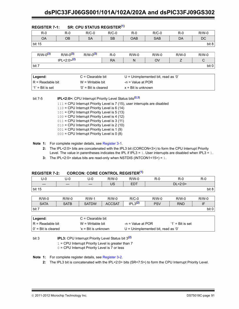
dsPIC33FJ06GS001/101A/102A/202A and dsPIC33FJ09GS302
REGISTER 7-1: SR: CPU STATUS REGISTER(1)
REGISTER 7-2: CORCON: CORE CONTROL REGISTER(1)
R-0 R-0 R/C-0 R/C-0 R-0 R/C-0 R-0 R/W-0
OA OB SA SB OAB SAB DA DC
bit 15 bit 8
R/W-0(3) R/W-0(3) R/W-0(3) R-0 R/W-0 R/W-0 R/W-0 R/W-0
IPL<2:0>(2) RA N OV Z C
bit 7 bit 0
Legend: C = Clearable bit U = Unimplemented bit, read as ‘0’
R = Readable bit W = Writable bit -n = Value at POR
‘1’ = Bit is set ‘0’ = Bit is cleared x = Bit is unknown
bit 7-5 IPL<2:0>: CPU Interrupt Priority Level Status bits(2,3)
111 = CPU Interrupt Priority Level is 7 (15), user interrupts are disabled110 = CPU Interrupt Priority Level is 6 (14)101 = CPU Interrupt Priority Level is 5 (13)100 = CPU Interrupt Priority Level is 4 (12)011 = CPU Interrupt Priority Level is 3 (11)010 = CPU Interrupt Priority Level is 2 (10)001 = CPU Interrupt Priority Level is 1 (9)000 = CPU Interrupt Priority Level is 0 (8)
Note 1: For complete register details, see Register 3-1.
2: The IPL<2:0> bits are concatenated with the IPL3 bit (CORCON<3>) to form the CPU Interrupt Priority Level. The value in parentheses indicates the IPL if IPL3 = 1. User interrupts are disabled when IPL3 = 1.
3: The IPL<2:0> status bits are read-only when NSTDIS (INTCON1<15>) = 1.
U-0 U-0 U-0 R/W-0 R/W-0 R-0 R-0 R-0
— — — US EDT DL<2:0>
bit 15 bit 8
R/W-0 R/W-0 R/W-1 R/W-0 R/C-0 R/W-0 R/W-0 R/W-0
SATA SATB SATDW ACCSAT IPL3(2) PSV RND IF
bit 7 bit 0
Legend: C = Clearable bit
R = Readable bit W = Writable bit -n = Value at POR ‘1’ = Bit is set
0’ = Bit is cleared ‘x = Bit is unknown U = Unimplemented bit, read as ‘0’
bit 3 IPL3: CPU Interrupt Priority Level Status bit 3(2)
1 = CPU Interrupt Priority Level is greater than 70 = CPU Interrupt Priority Level is 7 or less
Note 1: For complete register details, see Register 3-2.
2: The IPL3 bit is concatenated with the IPL<2:0> bits (SR<7:5>) to form the CPU Interrupt Priority Level.
2011-2012 Microchip Technology Inc. DS75018C-page 91

dsPIC33FJ06GS001/101A/102A/202A and dsPIC33FJ09GS302
REGISTER 7-3: INTCON1: INTERRUPT CONTROL REGISTER 1
R/W-0 R/W-0 R/W-0 R/W-0 R/W-0 R/W-0 R/W-0 R/W-0
NSTDIS OVAERR OVBERR COVAERR COVBERR OVATE OVBTE COVTE
bit 15 bit 8
R/W-0 R/W-0 U-0 R/W-0 R/W-0 R/W-0 R/W-0 U-0
SFTACERR DIV0ERR — MATHERR ADDRERR STKERR OSCFAIL —
bit 7 bit 0
Legend:
R = Readable bit W = Writable bit U = Unimplemented bit, read as ‘0’
-n = Value at POR ‘1’ = Bit is set ‘0’ = Bit is cleared x = Bit is unknown
bit 15 NSTDIS: Interrupt Nesting Disable bit
1 = Interrupt nesting is disabled0 = Interrupt nesting is enabled
bit 14 OVAERR: Accumulator A Overflow Trap Flag bit
1 = Trap was caused by overflow of Accumulator A0 = Trap was not caused by overflow of Accumulator A
bit 13 OVBERR: Accumulator B Overflow Trap Flag bit
1 = Trap was caused by overflow of Accumulator B0 = Trap was not caused by overflow of Accumulator B
bit 12 COVAERR: Accumulator A Catastrophic Overflow Trap Flag bit
1 = Trap was caused by catastrophic overflow of Accumulator A 0 = Trap was not caused by catastrophic overflow of Accumulator A
bit 11 COVBERR: Accumulator B Catastrophic Overflow Trap Flag bit
1 = Trap was caused by catastrophic overflow of Accumulator B 0 = Trap was not caused by catastrophic overflow of Accumulator B
bit 10 OVATE: Accumulator A Overflow Trap Enable bit
1 = Trap overflow of Accumulator A0 = Trap is disabled
bit 9 OVBTE: Accumulator B Overflow Trap Enable bit
1 = Trap overflow of Accumulator B0 = Trap is disabled
bit 8 COVTE: Catastrophic Overflow Trap Enable bit
1 = Trap on catastrophic overflow of Accumulator A or B is enabled0 = Trap is disabled
bit 7 SFTACERR: Shift Accumulator Error Status bit
1 = Math error trap was caused by an invalid accumulator shift0 = Math error trap was not caused by an invalid accumulator shift
bit 6 DIV0ERR: Divide-by-Zero Error Trap Status bit
1 = Math error trap was caused by a divide-by-zero0 = Math error trap was not caused by a divide-by-zero
bit 5 Unimplemented: Read as ‘0’
bit 4 MATHERR: Math Error Trap Status bit
1 = Math error trap has occurred0 = Math error trap has not occurred
bit 3 ADDRERR: Address Error Trap Status bit
1 = Address error trap has occurred0 = Address error trap has not occurred
DS75018C-page 92 2011-2012 Microchip Technology Inc.

dsPIC33FJ06GS001/101A/102A/202A and dsPIC33FJ09GS302
bit 2 STKERR: Stack Error Trap Status bit
1 = Stack error trap has occurred0 = Stack error trap has not occurred
bit 1 OSCFAIL: Oscillator Failure Trap Status bit
1 = Oscillator failure trap has occurred0 = Oscillator failure trap has not occurred
bit 0 Unimplemented: Read as ‘0’
REGISTER 7-3: INTCON1: INTERRUPT CONTROL REGISTER 1 (CONTINUED)
2011-2012 Microchip Technology Inc. DS75018C-page 93

dsPIC33FJ06GS001/101A/102A/202A and dsPIC33FJ09GS302
REGISTER 7-4: INTCON2: INTERRUPT CONTROL REGISTER 2
R/W-0 R-0 U-0 U-0 U-0 U-0 U-0 U-0
ALTIVT DISI — — — — — —
bit 15 bit 8
U-0 U-0 U-0 U-0 U-0 R/W-0 R/W-0 R/W-0
— — — — — INT2EP INT1EP INT0EP
bit 7 bit 0
Legend:
R = Readable bit W = Writable bit U = Unimplemented bit, read as ‘0’
-n = Value at POR ‘1’ = Bit is set ‘0’ = Bit is cleared x = Bit is unknown
bit 15 ALTIVT: Enable Alternate Interrupt Vector Table bit
1 = Uses alternate vector table0 = Uses standard (default) vector table
bit 14 DISI: DISI Instruction Status bit
1 = DISI instruction is active0 = DISI instruction is not active
bit 13-3 Unimplemented: Read as ‘0’
bit 2 INT2EP: External Interrupt 2 Edge Detect Polarity Select bit
1 = Interrupt on negative edge 0 = Interrupt on positive edge
bit 1 INT1EP: External Interrupt 1 Edge Detect Polarity Select bit
1 = Interrupt on negative edge 0 = Interrupt on positive edge
bit 0 INT0EP: External Interrupt 0 Edge Detect Polarity Select bit
1 = Interrupt on negative edge 0 = Interrupt on positive edge
DS75018C-page 94 2011-2012 Microchip Technology Inc.

dsPIC33FJ06GS001/101A/102A/202A and dsPIC33FJ09GS302
REGISTER 7-5: IFS0: INTERRUPT FLAG STATUS REGISTER 0
U-0 U-0 R/W-0 R/W-0 R/W-0 R/W-0 R/W-0 U-0
— — ADIF U1TXIF(1) U1RXIF(1) SPI1IF(1) SPI1EIF(1) —
bit 15 bit 8
R/W-0 U-0 U-0 U-0 R/W-0 R/W-0 R/W-0 R/W-0
T2IF — — — T1IF OC1IF(1) IC1IF(2) INT0IF
bit 7 bit 0
Legend:
R = Readable bit W = Writable bit U = Unimplemented bit, read as ‘0’
-n = Value at POR ‘1’ = Bit is set ‘0’ = Bit is cleared x = Bit is unknown
bit 15-14 Unimplemented: Read as ‘0’
bit 13 ADIF: ADC Group Conversion Complete Interrupt Flag Status bit
1 = Interrupt request has occurred0 = Interrupt request has not occurred
bit 12 U1TXIF: UART1 Transmitter Interrupt Flag Status bit(1)
1 = Interrupt request has occurred0 = Interrupt request has not occurred
bit 11 U1RXIF: UART1 Receiver Interrupt Flag Status bit(1)
1 = Interrupt request has occurred0 = Interrupt request has not occurred
bit 10 SPI1IF: SPI1 Event Interrupt Flag Status bit(1)
1 = Interrupt request has occurred0 = Interrupt request has not occurred
bit 9 SPI1EIF: SPI1 Error Interrupt Flag Status bit(1)
1 = Interrupt request has occurred0 = Interrupt request has not occurred
bit 8 Unimplemented: Read as ‘0’
bit 7 T2IF: Timer2 Interrupt Flag Status bit
1 = Interrupt request has occurred0 = Interrupt request has not occurred
bit 6-4 Unimplemented: Read as ‘0’
bit 3 T1IF: Timer1 Interrupt Flag Status bit
1 = Interrupt request has occurred0 = Interrupt request has not occurred
bit 2 OC1IF: Output Compare Channel 1 Interrupt Flag Status bit(1)
1 = Interrupt request has occurred0 = Interrupt request has not occurred
bit 1 IC1IF: Input Capture Channel 1 Interrupt Flag Status bit(2)
1 = Interrupt request has occurred0 = Interrupt request has not occurred
bit 0 INT0IF: External Interrupt 0 Flag Status bit
1 = Interrupt request has occurred0 = Interrupt request has not occurred
Note 1: This bit is not implemented in the dsPIC33FJ06GS001 device.
2: This bit is not implemented in dsPIC33FJ06GS001/101A/102A devices.
2011-2012 Microchip Technology Inc. DS75018C-page 95

dsPIC33FJ06GS001/101A/102A/202A and dsPIC33FJ09GS302
REGISTER 7-6: IFS1: INTERRUPT FLAG STATUS REGISTER 1
U-0 U-0 R/W-0 U-0 U-0 U-0 U-0 U-0
— — INT2IF — — — — —
bit 15 bit 8
U-0 U-0 U-0 R/W-0 R/W-0 R/W-0 R/W-0 R/W-0
— — — INT1IF CNIF AC1IF(1 MI2C1IF SI2C1IF
bit 7 bit 0
Legend:
R = Readable bit W = Writable bit U = Unimplemented bit, read as ‘0’
-n = Value at POR ‘1’ = Bit is set ‘0’ = Bit is cleared x = Bit is unknown
bit 15-14 Unimplemented: Read as ‘0’
bit 13 INT2IF: External Interrupt 2 Flag Status bit
1 = Interrupt request has occurred0 = Interrupt request has not occurred
bit 12-5 Unimplemented: Read as ‘0’
bit 4 INT1IF: External Interrupt 1 Flag Status bit
1 = Interrupt request has occurred0 = Interrupt request has not occurred
bit 3 CNIF: Input Change Notification Interrupt Flag Status bit
1 = Interrupt request has occurred0 = Interrupt request has not occurred
bit 2 AC1IF: Analog Comparator 1 Interrupt Flag Status bit(1)
1 = Interrupt request has occurred0 = Interrupt request has not occurred
bit 1 MI2C1IF: I2C1 Master Events Interrupt Flag Status bit
1 = Interrupt request has occurred0 = Interrupt request has not occurred
bit 0 SI2C1IF: I2C1 Slave Events Interrupt Flag Status bit
1 = Interrupt request has occurred0 = Interrupt request has not occurred
Note 1: This bit is not implemented in dsPIC33FJ06GS101A/102A devices.
DS75018C-page 96 2011-2012 Microchip Technology Inc.

dsPIC33FJ06GS001/101A/102A/202A and dsPIC33FJ09GS302
REGISTER 7-7: IFS3: INTERRUPT FLAG STATUS REGISTER 3
REGISTER 7-8: IFS4: INTERRUPT FLAG STATUS REGISTER 4
U-0 U-0 U-0 U-0 U-0 U-0 R/W-0 U-0
— — — — — — PSEMIF —
bit 15 bit 8
U-0 U-0 U-0 U-0 U-0 U-0 U-0 U-0
— — — — — — — —
bit 7 bit 0
Legend:
R = Readable bit W = Writable bit U = Unimplemented bit, read as ‘0’
-n = Value at POR ‘1’ = Bit is set ‘0’ = Bit is cleared x = Bit is unknown
bit 15-10 Unimplemented: Read as ‘0’
bit 9 PSEMIF: PWM Special Event Match Interrupt Flag Status bit
1 = Interrupt request has occurred0 = Interrupt request has not occurred
bit 8-0 Unimplemented: Read as ‘0’
U-0 U-0 U-0 U-0 U-0 U-0 U-0 U-0
— — — — — — — —
bit 15 bit 8
U-0 U-0 U-0 U-0 U-0 U-0 R/W-0 U-0
— — — — — — U1EIF(1) —
bit 7 bit 0
Legend:
R = Readable bit W = Writable bit U = Unimplemented bit, read as ‘0’
-n = Value at POR ‘1’ = Bit is set ‘0’ = Bit is cleared x = Bit is unknown
bit 15-2 Unimplemented: Read as ‘0’
bit 1 U1EIF: UART1 Error Interrupt Flag Status bit(1)
1 = Interrupt request has occurred0 = Interrupt request has not occurred
bit 0 Unimplemented: Read as ‘0’
Note 1: This bit is not implemented in the dsPIC33FJ06GS001 device.
2011-2012 Microchip Technology Inc. DS75018C-page 97

dsPIC33FJ06GS001/101A/102A/202A and dsPIC33FJ09GS302
REGISTER 7-9: IFS5: INTERRUPT FLAG STATUS REGISTER 5
R/W-0 R/W-0 U-0 U-0 U-0 U-0 U-0 U-0
PWM2IF(1) PWM1IF — — — — — —
bit 15 bit 8
U-0 U-0 U-0 U-0 U-0 U-0 U-0 R/W-0
— — — — — — — JTAGIF
bit 7 bit 0
Legend:
R = Readable bit W = Writable bit U = Unimplemented bit, read as ‘0’
-n = Value at POR ‘1’ = Bit is set ‘0’ = Bit is cleared x = Bit is unknown
bit 15 PWM2IF: PWM2 Interrupt Flag Status bit(1)
1 = Interrupt request has occurred0 = Interrupt request has not occurred
bit 14 PWM1IF: PWM1 Interrupt Flag Status bit
1 = Interrupt request has occurred0 = Interrupt request has not occurred
bit 13-1 Unimplemented: Read as ‘0’
bit 0 JTAGIF: JTAG Interrupt Flag Status bit
1 = Interrupt request has occurred0 = Interrupt request has not occurred
Note 1: This bit is not implemented in dsPIC33FJ06GS001/101A devices.
DS75018C-page 98 2011-2012 Microchip Technology Inc.

dsPIC33FJ06GS001/101A/102A/202A and dsPIC33FJ09GS302
REGISTER 7-10: IFS6: INTERRUPT FLAG STATUS REGISTER 6
R/W-0 R/W-0 U-0 U-0 U-0 U-0 U-0 U-0
ADCP1IF ADCP0IF — — — — — —
bit 15 bit 8
R/W-0 U-0 U-0 U-0 U-0 U-0 R/W-0 U-0
AC2IF(1) — — — — — PWM4IF(2) —
bit 7 bit 0
Legend:
R = Readable bit W = Writable bit U = Unimplemented bit, read as ‘0’
-n = Value at POR ‘1’ = Bit is set ‘0’ = Bit is cleared x = Bit is unknown
bit 15 ADCP1IF: ADC Pair 1 Conversion Done Interrupt Flag Status bit
1 = Interrupt request has occurred0 = Interrupt request has not occurred
bit 14 ADCP0IF: ADC Pair 0 Conversion Done Interrupt Flag Status bit
1 = Interrupt request has occurred0 = Interrupt request has not occurred
bit 13-8 Unimplemented: Read as ‘0’
bit 7 AC2IF: Analog Comparator 2 Interrupt Flag Status bit(1)
1 = Interrupt request has occurred0 = Interrupt request has not occurred
bit 6-2 Unimplemented: Read as ‘0’
bit 1 PWM4IF: PWM4 Interrupt Flag Status bit(2)
1 = Interrupt request has occurred0 = Interrupt request has not occurred
bit 0 Unimplemented: Read as ‘0’
Note 1: This bit is not implemented in dsPIC33FJ06GS101A/102A devices.
2: This bit is not implemented in dsPIC33FJ06GS102A/202A devices.
2011-2012 Microchip Technology Inc. DS75018C-page 99

dsPIC33FJ06GS001/101A/102A/202A and dsPIC33FJ09GS302
REGISTER 7-11: IFS7: INTERRUPT FLAG STATUS REGISTER 7
U-0 U-0 U-0 U-0 U-0 U-0 U-0 U-0
— — — — — — — —
bit 15 bit 8
U-0 U-0 U-0 R/W-0 U-0 U-0 R/W-0 R/W-0
— — — ADCP6IF — — ADCP3IF(1) ADCP2IF(2)
bit 7 bit 0
Legend:
R = Readable bit W = Writable bit U = Unimplemented bit, read as ‘0’
-n = Value at POR ‘1’ = Bit is set ‘0’ = Bit is cleared x = Bit is unknown
bit 15-5 Unimplemented: Read as ‘0’
bit 4 ADCP6IF: ADC Pair 6 Conversion Done Interrupt Flag Status bit
1 = Interrupt request has occurred0 = Interrupt request has not occurred
bit 3-2 Unimplemented: Read as ‘0’
bit 1 ADCP3IF: ADC Pair 3 Conversion Done Interrupt Flag Status bit(1)
1 = Interrupt request has occurred0 = Interrupt request has not occurred
bit 0 ADCP2IF: ADC Pair 2 Conversion Done Interrupt Flag Status bit(2)
1 = Interrupt request has occurred0 = Interrupt request has not occurred
Note 1: This bit is not implemented in dsPIC33FJ06GS102A/202A devices.
2: This bit is not implemented in dsPIC33FJ06GS001/101A devices.
DS75018C-page 100 2011-2012 Microchip Technology Inc.

dsPIC33FJ06GS001/101A/102A/202A and dsPIC33FJ09GS302
REGISTER 7-12: IEC0: INTERRUPT ENABLE CONTROL REGISTER 0
U-0 U-0 R/W-0 R/W-0 R/W-0 R/W-0 R/W-0 U-0
— — ADIE U1TXIE(1) U1RXIE(1) SPI1IE(1) SPI1EIE(1) —
bit 15 bit 8
R/W-0 U-0 U-0 U-0 R/W-0 R/W-0 R/W-0 R/W-0
T2IE — — — T1IE OC1IE(1) IC1IE(2) INT0IE
bit 7 bit 0
Legend:
R = Readable bit W = Writable bit U = Unimplemented bit, read as ‘0’
-n = Value at POR ‘1’ = Bit is set ‘0’ = Bit is cleared x = Bit is unknown
bit 15-14 Unimplemented: Read as ‘0’
bit 13 ADIE: ADC1 Conversion Complete Interrupt Enable bit
1 = Interrupt request is enabled0 = Interrupt request is not enabled
bit 12 U1TXIE: UART1 Transmitter Interrupt Enable bit(1)
1 = Interrupt request is enabled0 = Interrupt request is not enabled
bit 11 U1RXIE: UART1 Receiver Interrupt Enable bit(1)
1 = Interrupt request is enabled0 = Interrupt request is not enabled
bit 10 SPI1IE: SPI1 Event Interrupt Enable bit(1)
1 = Interrupt request is enabled0 = Interrupt request is not enabled
bit 9 SPI1EIE: SPI1 Event Interrupt Enable bit(1)
1 = Interrupt request is enabled0 = Interrupt request is not enabled
bit 8 Unimplemented: Read as ‘0’
bit 7 T2IE: Timer2 Interrupt Enable bit
1 = Interrupt request is enabled0 = Interrupt request is not enabled
bit 6-4 Unimplemented: Read as ‘0’
bit 3 T1IE: Timer1 Interrupt Enable bit
1 = Interrupt request is enabled0 = Interrupt request is not enabled
bit 2 OC1IE: Output Compare Channel 1 Interrupt Enable bit(1)
1 = Interrupt request is enabled0 = Interrupt request is not enabled
bit 1 IC1IE: Input Capture Channel 1 Interrupt Enable bit(2)
1 = Interrupt request is enabled0 = Interrupt request not enabled
bit 0 INT0IE: External Interrupt 0 Enable bit
1 = Interrupt request is enabled0 = Interrupt request is not enabled
Note 1: This bit is not implemented in dsPIC33FJ06GS001/101A/102A devices.
2: This bit is not implemented in the dsPIC33FJ06GS001 device.
2011-2012 Microchip Technology Inc. DS75018C-page 101

dsPIC33FJ06GS001/101A/102A/202A and dsPIC33FJ09GS302
REGISTER 7-13: IEC1: INTERRUPT ENABLE CONTROL REGISTER 1
U-0 U-0 R/W-0 U-0 U-0 U-0 U-0 U-0
— — INT2IE — — — — —
bit 15 bit 8
U-0 U-0 U-0 R/W-0 R/W-0 R/W-0 R/W-0 R/W-0
— — — INT1IE CNIE AC1IE(1) MI2C1IE SI2C1IE
bit 7 bit 0
Legend:
R = Readable bit W = Writable bit U = Unimplemented bit, read as ‘0’
-n = Value at POR ‘1’ = Bit is set ‘0’ = Bit is cleared x = Bit is unknown
bit 15-14 Unimplemented: Read as ‘0’
bit 13 INT2IE: External Interrupt 2 Enable bit
1 = Interrupt request is enabled0 = Interrupt request is not enabled
bit 12-5 Unimplemented: Read as ‘0’
bit 4 INT1IE: External Interrupt 1 Enable bit
1 = Interrupt request is enabled0 = Interrupt request is not enabled
bit 3 CNIE: Input Change Notification Interrupt Enable bit
1 = Interrupt request is enabled0 = Interrupt request is not enabled
bit 2 AC1IE: Analog Comparator 1 Interrupt Enable bit(1)
1 = Interrupt request is enabled0 = Interrupt request is not enabled
bit 1 MI2C1IE: I2C1 Master Events Interrupt Enable bit
1 = Interrupt request is enabled0 = Interrupt request is not enabled
bit 0 SI2C1IE: I2C1 Slave Events Interrupt Enable bit
1 = Interrupt request is enabled0 = Interrupt request is not enabled
Note 1: This bit is not implemented in dsPIC33FJ06GS101A/102A devices.
DS75018C-page 102 2011-2012 Microchip Technology Inc.

dsPIC33FJ06GS001/101A/102A/202A and dsPIC33FJ09GS302
REGISTER 7-14: IEC3: INTERRUPT ENABLE CONTROL REGISTER 3
REGISTER 7-15: IEC4: INTERRUPT ENABLE CONTROL REGISTER 4
U-0 U-0 U-0 U-0 U-0 U-0 R/W-0 U-0
— — — — — — PSEMIE —
bit 15 bit 8
U-0 U-0 U-0 U-0 U-0 U-0 U-0 U-0
— — — — — — — —
bit 7 bit 0
Legend:
R = Readable bit W = Writable bit U = Unimplemented bit, read as ‘0’
-n = Value at POR ‘1’ = Bit is set ‘0’ = Bit is cleared x = Bit is unknown
bit 15-10 Unimplemented: Read as ‘0’
bit 9 PSEMIE: PWM Special Event Match Interrupt Enable bit
1 = Interrupt request is enabled0 = Interrupt request is not enabled
bit 8-0 Unimplemented: Read as ‘0’
U-0 U-0 U-0 U-0 U-0 U-0 U-0 U-0
— — — — — — — —
bit 15 bit 8
U-0 U-0 U-0 U-0 U-0 U-0 R/W-0 U-0
— — — — — — U1EIE(1) —
bit 7 bit 0
Legend:
R = Readable bit W = Writable bit U = Unimplemented bit, read as ‘0’
-n = Value at POR ‘1’ = Bit is set ‘0’ = Bit is cleared x = Bit is unknown
bit 15-2 Unimplemented: Read as ‘0’
bit 1 U1EIE: UART1 Error Interrupt Enable bit(1)
1 = Interrupt request is enabled0 = Interrupt request is not enabled
bit 0 Unimplemented: Read as ‘0’
Note 1: This bit is not implemented in the dsPIC33FJ06GS001 device.
2011-2012 Microchip Technology Inc. DS75018C-page 103

dsPIC33FJ06GS001/101A/102A/202A and dsPIC33FJ09GS302
REGISTER 7-16: IEC5: INTERRUPT ENABLE CONTROL REGISTER 5
R/W-0 R/W-0 U-0 U-0 U-0 U-0 U-0 U-0
PWM2IE(1) PWM1IE — — — — — —
bit 15 bit 8
U-0 U-0 U-0 U-0 U-0 U-0 U-0 R/W-0
— — — — — — — JTAGIE
bit 7 bit 0
Legend:
R = Readable bit W = Writable bit U = Unimplemented bit, read as ‘0’
-n = Value at POR ‘1’ = Bit is set ‘0’ = Bit is cleared x = Bit is unknown
bit 15 PWM2IE: PWM2 Interrupt Enable bit(1)
1 = Interrupt request is enabled0 = Interrupt request is not enabled
bit 14 PWM1IE: PWM1 Interrupt Enable bit
1 = Interrupt request is enabled0 = Interrupt request is not enabled
bit 13-1 Unimplemented: Read as ‘0’
bit 0 JTAGIE: JTAG Interrupt Enable bit
1 = Interrupt request is enabled0 = Interrupt request is not enabled
Note 1: This bit is not implemented in dsPIC33FJ06GS001/101A devices.
DS75018C-page 104 2011-2012 Microchip Technology Inc.

dsPIC33FJ06GS001/101A/102A/202A and dsPIC33FJ09GS302
REGISTER 7-17: IEC6: INTERRUPT ENABLE CONTROL REGISTER 6
R/W-0 R/W-0 U-0 U-0 U-0 U-0 U-0 U-0
ADCP1IE ADCP0IE — — — — — —
bit 15 bit 8
R/W-0 U-0 U-0 U-0 U-0 U-0 R/W-0 U-0
AC2IE(1) — — — — — PWM4IE(2) —
bit 7 bit 0
Legend:
R = Readable bit W = Writable bit U = Unimplemented bit, read as ‘0’
-n = Value at POR ‘1’ = Bit is set ‘0’ = Bit is cleared x = Bit is unknown
bit 15 ADCP1IE: ADC Pair 1 Conversion Done Interrupt Enable bit
1 = Interrupt request is enabled0 = Interrupt request is not enabled
bit 14 ADCP0IE: ADC Pair 0 Conversion Done Interrupt Enable bit
1 = Interrupt request is enabled0 = Interrupt request is not enabled
bit 13-8 Unimplemented: Read as ‘0
bit 7 AC2IE: Analog Comparator 2 Interrupt Enable bit(1)
1 = Interrupt request is enabled0 = Interrupt request is not enabled
bit 6-2 Unimplemented: Read as ‘0’
bit 1 PWM4IE: PWM4 Interrupt Enable bit(2)
1 = Interrupt request is enabled0 = Interrupt request is not enabled
bit 0 Unimplemented: Read as ‘0’
Note 1: This bit is not implemented in dsPIC33FJ06GS101A/102A devices.
2: This bit is not implemented in dsPIC33FJ06GS102A/202A devices.
2011-2012 Microchip Technology Inc. DS75018C-page 105

dsPIC33FJ06GS001/101A/102A/202A and dsPIC33FJ09GS302
REGISTER 7-18: IEC7: INTERRUPT ENABLE CONTROL REGISTER 7
U-0 U-0 U-0 U-0 U-0 U-0 U-0 U-0
— — — — — — — —
bit 15 bit 8
U-0 U-0 U-0 R/W-0 U-0 U-0 R/W-0 R/W-0
— — — ADCP6IE — — ADCP3IE(1) ADCP2IE(2)
bit 7 bit 0
Legend:
R = Readable bit W = Writable bit U = Unimplemented bit, read as ‘0’
-n = Value at POR ‘1’ = Bit is set ‘0’ = Bit is cleared x = Bit is unknown
bit 15-5 Unimplemented: Read as ‘0’
bit 4 ADCP6IE: ADC Pair 6 Conversion Done Interrupt Enable bit
1 = Interrupt request is enabled0 = Interrupt request is not enabled
bit 3-2 Unimplemented: Read as ‘0’
bit 1 ADCP3IE: ADC Pair 3 Conversion Done Interrupt Enable bit(1)
1 = Interrupt request is enabled0 = Interrupt request is not enabled
bit 0 ADCP2IE: ADC Pair 2 Conversion Done Interrupt Enable bit(2)
1 = Interrupt request is enabled0 = Interrupt request is not enabled
Note 1: This bit is not implemented in dsPIC33FJ06GS102A/202A devices.
2: This bit is not implemented in dsPIC33FJ06GS001/101A devices.
DS75018C-page 106 2011-2012 Microchip Technology Inc.

dsPIC33FJ06GS001/101A/102A/202A and dsPIC33FJ09GS302
REGISTER 7-19: IPC0: INTERRUPT PRIORITY CONTROL REGISTER 0
U-0 R/W-1 R/W-0 R/W-0 U-0 R/W-1 R/W-0 R/W-0
— T1IP<2:0> — OC1IP<2:0>(1)
bit 15 bit 8
U-0 R/W-1 R/W-0 R/W-0 U-0 R/W-1 R/W-0 R/W-0
— IC1IP<2:0>(2) — INT0IP<2:0>
bit 7 bit 0
Legend:
R = Readable bit W = Writable bit U = Unimplemented bit, read as ‘0’
-n = Value at POR ‘1’ = Bit is set ‘0’ = Bit is cleared x = Bit is unknown
bit 15 Unimplemented: Read as ‘0’
bit 14-12 T1IP<2:0>: Timer1 Interrupt Priority bits
111 = Interrupt is Priority 7 (highest priority interrupt)•••001 = Interrupt is Priority 1000 = Interrupt source is disabled
bit 11 Unimplemented: Read as ‘0’
bit 10-8 OC1IP<2:0>: Output Compare Channel 1 Interrupt Priority bits(1)
111 = Interrupt is Priority 7 (highest priority interrupt)•••001 = Interrupt is Priority 1000 = Interrupt source is disabled
bit 7 Unimplemented: Read as ‘0’
bit 6-4 IC1IP<2:0>: Input Capture Channel 1 Interrupt Priority bits(2)
111 = Interrupt is Priority 7 (highest priority interrupt)•••001 = Interrupt is Priority 1000 = Interrupt source is disabled
bit 3 Unimplemented: Read as ‘0’
bit 2-0 INT0IP<2:0>: External Interrupt 0 Priority bits
111 = Interrupt is Priority 7 (highest priority interrupt)•••001 = Interrupt is Priority 1000 = Interrupt source is disabled
Note 1: These bits are not implemented in the dsPIC33FJ06GS001 device.
2: These bits are not implemented in dsPIC33FJ06GS001/101A/102A devices.
2011-2012 Microchip Technology Inc. DS75018C-page 107

dsPIC33FJ06GS001/101A/102A/202A and dsPIC33FJ09GS302
REGISTER 7-20: IPC1: INTERRUPT PRIORITY CONTROL REGISTER 1
U-0 R/W-1 R/W-0 R/W-0 U-0 U-0 U-0 U-0
— T2IP<2:0> — — — —
bit 15 bit 8
U-0 U-0 U-0 U-0 U-0 U-0 U-0 U-0
— — — — — — — —
bit 7 bit 0
Legend:
R = Readable bit W = Writable bit U = Unimplemented bit, read as ‘0’
-n = Value at POR ‘1’ = Bit is set ‘0’ = Bit is cleared x = Bit is unknown
bit 15 Unimplemented: Read as ‘0’
bit 14-12 T2IP<2:0>: Timer2 Interrupt Priority bits
111 = Interrupt is Priority 7 (highest priority interrupt)•••001 = Interrupt is Priority 1000 = Interrupt source is disabled
bit 11-0 Unimplemented: Read as ‘0’
DS75018C-page 108 2011-2012 Microchip Technology Inc.

dsPIC33FJ06GS001/101A/102A/202A and dsPIC33FJ09GS302
REGISTER 7-21: IPC2: INTERRUPT PRIORITY CONTROL REGISTER 2
U-0 R/W-1 R/W-0 R/W-0 U-0 R/W-1 R/W-0 R/W-0
— U1RXIP<2:0>(1) — SPI1IP<2:0>(1)
bit 15 bit 8
U-0 R/W-1 R/W-0 R/W-0 U-0 U-0 U-0 U-0
— SPI1EIP<2:0>(1) — — — —
bit 7 bit 0
Legend:
R = Readable bit W = Writable bit U = Unimplemented bit, read as ‘0’
-n = Value at POR ‘1’ = Bit is set ‘0’ = Bit is cleared x = Bit is unknown
bit 15 Unimplemented: Read as ‘0’
bit 14-12 U1RXIP<2:0>: UART1 Receiver Interrupt Priority bits(1)
111 = Interrupt is Priority 7 (highest priority interrupt)•••001 = Interrupt is Priority 1000 = Interrupt source is disabled
bit 11 Unimplemented: Read as ‘0’
bit 10-8 SPI1IP<2:0>: SPI1 Event Interrupt Priority bits(1)
111 = Interrupt is Priority 7 (highest priority interrupt)•••001 = Interrupt is Priority 1000 = Interrupt source is disabled
bit 7 Unimplemented: Read as ‘0’
bit 6-4 SPI1EIP<2:0>: SPI1 Error Interrupt Priority bits(1)
111 = Interrupt is Priority 7 (highest priority interrupt)•••001 = Interrupt is Priority 1000 = Interrupt source is disabled
bit 3-0 Unimplemented: Read as ‘0’
Note 1: These bits are not implemented in the dsPIC33FJ06GS001 device.
2011-2012 Microchip Technology Inc. DS75018C-page 109

dsPIC33FJ06GS001/101A/102A/202A and dsPIC33FJ09GS302
REGISTER 7-22: IPC3: INTERRUPT PRIORITY CONTROL REGISTER 3
U-0 U-0 U-0 U-0 U-0 U-0 U-0 U-0
— — — — — — — —
bit 15 bit 8
U-0 R/W-1 R/W-0 R/W-0 U-0 R/W-1 R/W-0 R/W-0
— ADIP<2:0> — U1TXIP<2:0>(1)
bit 7 bit 0
Legend:
R = Readable bit W = Writable bit U = Unimplemented bit, read as ‘0’
-n = Value at POR ‘1’ = Bit is set ‘0’ = Bit is cleared x = Bit is unknown
bit 15-7 Unimplemented: Read as ‘0’
bit 6-4 ADIP<2:0>: ADC1 Conversion Complete Interrupt Priority bits
111 = Interrupt is Priority 7 (highest priority interrupt)•••001 = Interrupt is Priority 1000 = Interrupt source is disabled
bit 3 Unimplemented: Read as ‘0’
bit 2-0 U1TXIP<2:0>: UART1 Transmitter Interrupt Priority bits(1)
111 = Interrupt is Priority 7 (highest priority interrupt)•••001 = Interrupt is Priority 1000 = Interrupt source is disabled
Note 1: These bits are not implemented in the dsPIC33FJ06GS001 device.
DS75018C-page 110 2011-2012 Microchip Technology Inc.

dsPIC33FJ06GS001/101A/102A/202A and dsPIC33FJ09GS302
REGISTER 7-23: IPC4: INTERRUPT PRIORITY CONTROL REGISTER 4
U-0 R/W-1 R/W-0 R/W-0 U-0 R/W-1 R/W-0 R/W-0
— CNIP<2:0> — AC1IP<2:0>(1)
bit 15 bit 8
U-0 R/W-1 R/W-0 R/W-0 U-0 R/W-1 R/W-0 R/W-0
— MI2C1IP<2:0> — SI2C1IP<2:0>
bit 7 bit 0
Legend:
R = Readable bit W = Writable bit U = Unimplemented bit, read as ‘0’
-n = Value at POR ‘1’ = Bit is set ‘0’ = Bit is cleared x = Bit is unknown
bit 15 Unimplemented: Read as ‘0’
bit 14-12 CNIP<2:0>: Change Notification Interrupt Priority bits
111 = Interrupt is Priority 7 (highest priority interrupt)•••001 = Interrupt is Priority 1000 = Interrupt source is disabled
bit 11 Unimplemented: Read as ‘0’
bit 10-8 AC1IP<2:0>: Analog Comparator 1 Interrupt Priority bits(1)
111 = Interrupt is Priority 7 (highest priority interrupt)•••001 = Interrupt is Priority 1000 = Interrupt source is disabled
bit 7 Unimplemented: Read as ‘0’
bit 6-4 MI2C1IP<2:0>: I2C1 Master Events Interrupt Priority bits
111 = Interrupt is Priority 7 (highest priority interrupt)•••001 = Interrupt is Priority 1000 = Interrupt source is disabled
bit 3 Unimplemented: Read as ‘0’
bit 2-0 SI2C1IP<2:0>: I2C1 Slave Events Interrupt Priority bits
111 = Interrupt is Priority 7 (highest priority interrupt)•••001 = Interrupt is Priority 1000 = Interrupt source is disabled
Note 1: These bits are not implemented in dsPIC33FJ06GS101A/102A devices.
2011-2012 Microchip Technology Inc. DS75018C-page 111

dsPIC33FJ06GS001/101A/102A/202A and dsPIC33FJ09GS302
REGISTER 7-24: IPC5: INTERRUPT PRIORITY CONTROL REGISTER 5
REGISTER 7-25: IPC7: INTERRUPT PRIORITY CONTROL REGISTER 7
U-0 U-0 U-0 U-0 U-0 U-0 U-0 U-0
— — — — — — — —
bit 15 bit 8
U-0 U-0 U-0 U-0 U-0 R/W-1 R/W-0 R/W-0
— — — — — INT1IP<2:0>
bit 7 bit 0
Legend:
R = Readable bit W = Writable bit U = Unimplemented bit, read as ‘0’
-n = Value at POR ‘1’ = Bit is set ‘0’ = Bit is cleared x = Bit is unknown
bit 15-3 Unimplemented: Read as ‘0’
bit 2-0 INT1IP<2:0>: External Interrupt 1 Priority bits
111 = Interrupt is Priority 7 (highest priority interrupt)•••001 = Interrupt is Priority 1000 = Interrupt source is disabled
U-0 U-1 U-0 U-0 U-0 U-0 U-0 U-0
— — — — — — — —
bit 15 bit 8
U-0 R/W-1 R/W-0 R/W-0 U-0 U-0 U-0 U-0
— INT2IP<2:0> — — — —
bit 7 bit 0
Legend:
R = Readable bit W = Writable bit U = Unimplemented bit, read as ‘0’
-n = Value at POR ‘1’ = Bit is set ‘0’ = Bit is cleared x = Bit is unknown
bit 15-7 Unimplemented: Read as ‘0’
bit 6-4 INT2IP<2:0>: External Interrupt 2 Priority bits
111 = Interrupt is Priority 7 (highest priority interrupt)•••001 = Interrupt is Priority 1000 = Interrupt source is disabled
bit 3-0 Unimplemented: Read as ‘0’
DS75018C-page 112 2011-2012 Microchip Technology Inc.

dsPIC33FJ06GS001/101A/102A/202A and dsPIC33FJ09GS302
REGISTER 7-26: IPC14: INTERRUPT PRIORITY CONTROL REGISTER 14
REGISTER 7-27: IPC16: INTERRUPT PRIORITY CONTROL REGISTER 16
U-0 U-0 U-0 U-0 U-0 U-0 U-0 U-0
— — — — — — — —
bit 15 bit 8
U-0 R/W-1 R/W-0 R/W-0 U-0 U-0 U-0 U-0
— PSEMIP<2:0> — — — —
bit 7 bit 0
Legend:
R = Readable bit W = Writable bit U = Unimplemented bit, read as ‘0’
-n = Value at POR ‘1’ = Bit is set ‘0’ = Bit is cleared x = Bit is unknown
bit 15-7 Unimplemented: Read as ‘0’
bit 6-4 PSEMIP<2:0>: PWM Special Event Match Interrupt Priority bits
111 = Interrupt is Priority 7 (highest priority interrupt)•••001 = Interrupt is Priority 1000 = Interrupt source is disabled
bit 3-0 Unimplemented: Read as ‘0’
U-0 U-0 U-0 U-0 U-0 U-0 U-0 U-0
— — — — — — — —
bit 15 bit 8
U-0 R/W-1 R/W-0 R/W-0 U-0 U-0 U-0 U-0
— U1EIP<2:0>(1) — — — —
bit 7 bit 0
Legend:
R = Readable bit W = Writable bit U = Unimplemented bit, read as ‘0’
-n = Value at POR ‘1’ = Bit is set ‘0’ = Bit is cleared x = Bit is unknown
bit 15-7 Unimplemented: Read as ‘0’
bit 6-4 U1EIP<2:0>: UART1 Error Interrupt Priority bits(1)
111 = Interrupt is Priority 7 (highest priority interrupt)•••001 = Interrupt is Priority 1000 = Interrupt source is disabled
bit 3-0 Unimplemented: Read as ‘0’
Note 1: These bits are not implemented in the dsPIC33FJ06GS001 device.
2011-2012 Microchip Technology Inc. DS75018C-page 113

dsPIC33FJ06GS001/101A/102A/202A and dsPIC33FJ09GS302
REGISTER 7-28: IPC20: INTERRUPT PRIORITY CONTROL REGISTER 20
U-0 U-0 U-0 U-0 U-0 U-0 U-0 U-0
— — — — — — — —
bit 15 bit 8
U-0 U-0 U-0 U-0 U-0 R/W-1 R/W-0 R/W-0
— — — — — JTAGIP<2:0>
bit 7 bit 0
Legend:
R = Readable bit W = Writable bit U = Unimplemented bit, read as ‘0’
-n = Value at POR ‘1’ = Bit is set ‘0’ = Bit is cleared x = Bit is unknown
bit 15-3 Unimplemented: Read as ‘0’
bit 2-0 JTAGIP<2:0>: JTAG Interrupt Priority bits
111 = Interrupt is Priority 7 (highest priority interrupt)•••001 = Interrupt is Priority 1000 = Interrupt source is disabled
DS75018C-page 114 2011-2012 Microchip Technology Inc.

dsPIC33FJ06GS001/101A/102A/202A and dsPIC33FJ09GS302
REGISTER 7-29: IPC23: INTERRUPT PRIORITY CONTROL REGISTER 23
U-0 R/W-1 R/W-0 R/W-0 U-0 R/W-1 R/W-0 R/W-0
— PWM2IP(1) — PWM1IP<2:0>
bit 15 bit 8
U-0 U-0 U-0 U-0 U-0 U-0 U-0 U-0
— — — — — — — —
bit 7 bit 0
Legend:
R = Readable bit W = Writable bit U = Unimplemented bit, read as ‘0’
-n = Value at POR ‘1’ = Bit is set ‘0’ = Bit is cleared x = Bit is unknown
bit 15 Unimplemented: Read as ‘0’
bit 14-12 PWM2IP<2:0>: PWM2 Interrupt Priority bits(1)
111 = Interrupt is Priority 7 (highest priority)
•
•
•
001 = Interrupt is Priority 1000 = Interrupt source is disabled
bit 11 Unimplemented: Read as ‘0’
bit 10-8 PWM1IP<2:0>: PWM1 Interrupt Priority bits
111 = Interrupt is Priority 7 (highest priority)
•
•
•
001 = Interrupt is Priority 1000 = Interrupt source is disabled
bit 7-0 Unimplemented: Read as ‘0’
Note 1: These bits are not implemented in dsPIC33FJ06GS001/101A devices.
2011-2012 Microchip Technology Inc. DS75018C-page 115

dsPIC33FJ06GS001/101A/102A/202A and dsPIC33FJ09GS302
REGISTER 7-30: IPC24: INTERRUPT PRIORITY CONTROL REGISTER 24
U-0 U-0 U-0 U-0 U-0 U-0 U-0 U-0
— — — — — — — —
bit 15 bit 8
U-0 R/W-1 R/W-0 R/W-0 U-0 U-0 U-0 U-0
— PWM4IP(1) — — — —
bit 7 bit 0
Legend:
R = Readable bit W = Writable bit U = Unimplemented bit, read as ‘0’
-n = Value at POR ‘1’ = Bit is set ‘0’ = Bit is cleared x = Bit is unknown
bit 15-7 Unimplemented: Read as ‘0’
bit 6-4 PWM4IP<2:0>: PWM4 Interrupt Priority bits(1)
111 = Interrupt is Priority 7 (highest priority)
•
•
•
001 = Interrupt is Priority 1000 = Interrupt source is disabled
bit 3-0 Unimplemented: Read as ‘0’
Note 1: These bits are not implemented in dsPIC33FJ06GS102A/202A devices.
DS75018C-page 116 2011-2012 Microchip Technology Inc.

dsPIC33FJ06GS001/101A/102A/202A and dsPIC33FJ09GS302
REGISTER 7-31: IPC25: INTERRUPT PRIORITY CONTROL REGISTER 25
U-0 R/W-1 R/W-0 R/W-0 U-0 U-0 U-0 U-0
— AC2IP<2:0>(1) — — — —
bit 15 bit 8
U-0 U-0 U-0 U-0 U-0 U-0 U-0 U-0
— — — — — — — —
bit 7 bit 0
Legend:
R = Readable bit W = Writable bit U = Unimplemented bit, read as ‘0’
-n = Value at POR ‘1’ = Bit is set ‘0’ = Bit is cleared x = Bit is unknown
bit 15 Unimplemented: Read as ‘0’
bit 14-12 AC2IP<2:0>: Analog Comparator 2 Interrupt Priority bits(1)
111 = Interrupt is Priority 7 (highest priority)
•
•
•
001 = Interrupt is Priority 1000 = Interrupt source is disabled
bit 11-0 Unimplemented: Read as ‘0’
Note 1: These bits are not implemented in dsPIC33FJ06GS101A/102A devices.
2011-2012 Microchip Technology Inc. DS75018C-page 117
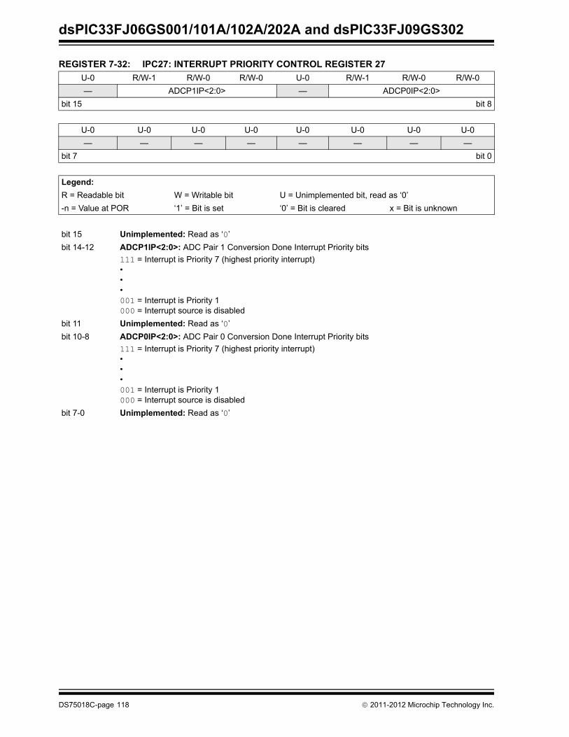
dsPIC33FJ06GS001/101A/102A/202A and dsPIC33FJ09GS302
REGISTER 7-32: IPC27: INTERRUPT PRIORITY CONTROL REGISTER 27
U-0 R/W-1 R/W-0 R/W-0 U-0 R/W-1 R/W-0 R/W-0
— ADCP1IP<2:0> — ADCP0IP<2:0>
bit 15 bit 8
U-0 U-0 U-0 U-0 U-0 U-0 U-0 U-0
— — — — — — — —
bit 7 bit 0
Legend:
R = Readable bit W = Writable bit U = Unimplemented bit, read as ‘0’
-n = Value at POR ‘1’ = Bit is set ‘0’ = Bit is cleared x = Bit is unknown
bit 15 Unimplemented: Read as ‘0’
bit 14-12 ADCP1IP<2:0>: ADC Pair 1 Conversion Done Interrupt Priority bits
111 = Interrupt is Priority 7 (highest priority interrupt)•••001 = Interrupt is Priority 1000 = Interrupt source is disabled
bit 11 Unimplemented: Read as ‘0’
bit 10-8 ADCP0IP<2:0>: ADC Pair 0 Conversion Done Interrupt Priority bits
111 = Interrupt is Priority 7 (highest priority interrupt)•••001 = Interrupt is Priority 1000 = Interrupt source is disabled
bit 7-0 Unimplemented: Read as ‘0’
DS75018C-page 118 2011-2012 Microchip Technology Inc.

dsPIC33FJ06GS001/101A/102A/202A and dsPIC33FJ09GS302
REGISTER 7-33: IPC28: INTERRUPT PRIORITY CONTROL REGISTER 28
U-0 U-0 U-0 U-0 U-0 U-0 U-0 U-0
— — — — — — — —
bit 15 bit 8
U-0 R/W-1 R/W-0 R/W-0 U-0 R/W-1 R/W-0 R/W-0
— ADCP3IP<2:0>(1) — ADCP2IP<2:0>(2)
bit 7 bit 0
Legend:
R = Readable bit W = Writable bit U = Unimplemented bit, read as ‘0’
-n = Value at POR ‘1’ = Bit is set ‘0’ = Bit is cleared x = Bit is unknown
bit 15-7 Unimplemented: Read as ‘0’
bit 6-4 ADCP3IP<2:0>: ADC Pair 3 Conversion Done Interrupt Priority bits(1)
111 = Interrupt is Priority 7 (highest priority interrupt)•••001 = Interrupt is Priority 1000 = Interrupt source is disabled
bit 3 Unimplemented: Read as ‘0’
bit 2-0 ADCP2IP<2:0>: ADC Pair 2 Conversion Done Interrupt Priority bits(2)
111 = Interrupt is Priority 7 (highest priority interrupt)•••001 = Interrupt is Priority 1000 = Interrupt source is disabled
Note 1: These bits are not implemented in dsPIC33FJ06GS102A/202A devices.
2: These bits are not implemented in dsPIC33FJ06GS001/101A devices.
2011-2012 Microchip Technology Inc. DS75018C-page 119

dsPIC33FJ06GS001/101A/102A/202A and dsPIC33FJ09GS302
REGISTER 7-34: IPC29: INTERRUPT PRIORITY CONTROL REGISTER 29
U-0 U-0 U-0 U-0 U-0 U-0 U-0 U-0
— — — — — — — —
bit 15 bit 8
U-0 U-0 U-0 U-0 U-0 R/W-1 R/W-0 R/W-0
— — — — — ADCP6IP<2:0>
bit 7 bit 0
Legend:
R = Readable bit W = Writable bit U = Unimplemented bit, read as ‘0’
-n = Value at POR ‘1’ = Bit is set ‘0’ = Bit is cleared x = Bit is unknown
bit 15-3 Unimplemented: Read as ‘0’
bit 2-0 ADCP6IP<2:0>: ADC Pair 6 Conversion Done Interrupt Priority bits
111 = Interrupt is Priority 7 (highest priority interrupt)•••001 = Interrupt is Priority 1000 = Interrupt source is disabled
DS75018C-page 120 2011-2012 Microchip Technology Inc.

dsPIC33FJ06GS001/101A/102A/202A and dsPIC33FJ09GS302
REGISTER 7-35: INTTREG: INTERRUPT CONTROL AND STATUS REGISTER
U-0 U-0 U-0 U-0 R-0 R-0 R-0 R-0
— — — — ILR<3:0>
bit 15 bit 8
U-0 R-0 R-0 R-0 R-0 R-0 R-0 R-0
— VECNUM<6:0>
bit 7 bit 0
Legend:
R = Readable bit W = Writable bit U = Unimplemented bit, read as ‘0’
-n = Value at POR ‘1’ = Bit is set ‘0’ = Bit is cleared x = Bit is unknown
bit 15-12 Unimplemented: Read as ‘0’
bit 11-8 ILR<3:0>: New CPU Interrupt Priority Level bits
1111 = CPU Interrupt Priority Level is 15 •••0001 = CPU Interrupt Priority Level is 10000 = CPU Interrupt Priority Level is 0
bit 7 Unimplemented: Read as ‘0’
bit 6-0 VECNUM<6:0>: Vector Number of Pending Interrupt bits
0111111 = Interrupt vector pending is Number 135 •••0000001 = Interrupt vector pending is Number 90000000 = Interrupt vector pending is Number 8
2011-2012 Microchip Technology Inc. DS75018C-page 121
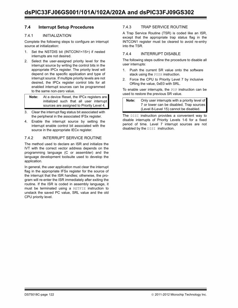
dsPIC33FJ06GS001/101A/102A/202A and dsPIC33FJ09GS302
7.4 Interrupt Setup Procedures
7.4.1 INITIALIZATION
Complete the following steps to configure an interruptsource at initialization:
1. Set the NSTDIS bit (INTCON1<15>) if nestedinterrupts are not desired.
2. Select the user-assigned priority level for theinterrupt source by writing the control bits in theappropriate IPCx register. The priority level willdepend on the specific application and type ofinterrupt source. If multiple priority levels are notdesired, the IPCx register control bits for allenabled interrupt sources can be programmedto the same non-zero value.
3. Clear the interrupt flag status bit associated withthe peripheral in the associated IFSx register.
4. Enable the interrupt source by setting theinterrupt enable control bit associated with thesource in the appropriate IECx register.
7.4.2 INTERRUPT SERVICE ROUTINE
The method used to declare an ISR and initialize theIVT with the correct vector address depends on theprogramming language (C or assembler) and thelanguage development toolsuite used to develop theapplication.
In general, the user application must clear the interruptflag in the appropriate IFSx register for the source ofthe interrupt that the ISR handles; otherwise, the pro-gram will re-enter the ISR immediately after exiting theroutine. If the ISR is coded in assembly language, itmust be terminated using a RETFIE instruction tounstack the saved PC value, SRL value and the oldCPU priority level.
7.4.3 TRAP SERVICE ROUTINE
A Trap Service Routine (TSR) is coded like an ISR,except that the appropriate trap status flag in theINTCON1 register must be cleared to avoid re-entryinto the TSR.
7.4.4 INTERRUPT DISABLE
The following steps outline the procedure to disable alluser interrupts:
1. Push the current SR value onto the softwarestack using the PUSH instruction.
2. Force the CPU to Priority Level 7 by inclusiveORing the value, 0xE0 with SRL.
To enable user interrupts, the POP instruction can beused to restore the previous SR value.
The DISI instruction provides a convenient way todisable interrupts of Priority Levels 1-6 for a fixedperiod of time. Level 7 interrupt sources are notdisabled by the DISI instruction.
Note: At a device Reset, the IPCx registers areinitialized such that all user interruptsources are assigned to Priority Level 4.
Note: Only user interrupts with a priority level of7 or lower can be disabled. Trap sources(Level 8-Level 15) cannot be disabled.
DS75018C-page 122 2011-2012 Microchip Technology Inc.

dsPIC33FJ06GS001/101A/102A/202A and dsPIC33FJ09GS302
8.0 OSCILLATOR CONFIGURATION The oscillator system provides:• External and internal oscillator options as clock
sources• An on-chip Phase Lock Loop (PLL) to scale the
internal operating frequency to the required system clock frequency
• An internal FRC oscillator that can also be used with the PLL, thereby allowing full-speed operation without any external clock generation hardware
• Clock switching between various clock sources• Programmable clock postscaler for system power
savings• A Fail-Safe Clock Monitor (FSCM) that detects clock
failure and takes fail-safe measures• An Oscillator Control register (OSCCON)• Nonvolatile Configuration bits for main oscillator
selection• An auxiliary PLL for ADC and PWMA simplified diagram of the oscillator system is shownin Figure 8-1.
FIGURE 8-1: OSCILLATOR SYSTEM DIAGRAM
Note 1: This data sheet summarizes the featuresof the dsPIC33FJ06GS001/101A/102A/202A and dsPIC33FJ09GS302 familiesof devices. It is not intended to be acomprehensive reference source. Tocomplement the information in this datasheet, refer to Section 42. “Oscillator(Part IV)” (DS70307) in the “dsPIC33F/PIC24H Family Reference Manual”,which is available from the Microchip website (www.microchip.com).
2: Some registers and associated bitsdescribed in this section may not beavailable on all devices. Refer toSection 4.0 “Memory Organization” inthis data sheet for device-specific registerand bit information.
XTPLL, HSPLL,
XT, HS, EC
FRCDIV<2:0>
WDT, PWRT,FSCM
FRCDIVN
FRCDIV16
ECPLL, FRCPLL
NOSC<2:0> FNOSC<2:0>
Reset
LPRCOscillator
DOZE<2:0>
S3
S1
S2
S1/S3
S7
S6
FRC
LPRC
S0
S5
÷ 16
Clock Switch
S7
Clock Fail
÷ 2
TUN<5:0>
PLL(1)
FCY(3)
FOSCFR
CD
IV
DO
ZE
ACLK, FADC
SELACLK APSTSCLR<2:0>
To PWM/ADC(1)
ENAPLL
POSCMD<1:0>FVCO(1)
APLL(1)
x16
ASRCSEL FRCSEL
POSCCLKFRCCLK
FRCCLK
POSCCLK
ROSEL RODIV<3:0>
REFCLKO
POSCCLK
Reference Clock Generation
Auxiliary Clock Generation
RPx
Note 1: See Section 8.1.3 “PLL Configuration” and Section 8.2 “Auxiliary Clock Generation” for configuration restrictions.
2: If the oscillator is used with XT or HS modes, an external parallel resistor with the value of 1 M must be connected.
3: The term, FP, refers to the clock source for all the peripherals, while FCY refers to the clock source for the CPU. Throughout thisdocument, FP and FCY are used interchangeably, except in the case of Doze mode. FP and FCY will be different when Doze mode isused in any ratio other than 1:1, which is the default.
FVCO(1)
FOSC
FP(3)
OSC2
OSC1Primary Oscillator
R(2)
To LFSR
FRCOscillator
÷ N
÷ N
2011-2012 Microchip Technology Inc. DS75018C-page 123

dsPIC33FJ06GS001/101A/102A/202A and dsPIC33FJ09GS302
8.1 CPU Clocking System
The devices provide six system clock options:
• Fast RC (FRC) Oscillator
• FRC Oscillator with PLL
• Primary (XT, HS or EC) Oscillator
• Primary Oscillator with PLL
• Low-Power RC (LPRC) Oscillator
• FRC Oscillator with Postscaler
8.1.1 SYSTEM CLOCK SOURCES
The Fast RC (FRC) internal oscillator runs at a nominalfrequency of 7.37 MHz. User software can tune theFRC frequency. User software can optionally specify afactor (ranging from 1:2 to 1:256) by which the FRCclock frequency is divided. This factor is selected usingthe FRCDIV<2:0> (CLKDIV<10:8>) bits.
The primary oscillator can use one of the following asits clock source:
• XT (Crystal): Crystals and ceramic resonators in the range of 3 MHz to 10 MHz. The crystal is connected to the OSC1 and OSC2 pins.
• HS (High-Speed Crystal): Crystals in the range of 10 MHz to 32 MHz. The crystal is connected to the OSC1 and OSC2 pins.
• EC (External Clock): The external clock signal is directly applied to the OSC1 pin.
The LPRC internal oscIllator runs at a nominalfrequency of 32.768 kHz. It is also used as a referenceclock by the Watchdog Timer (WDT) and Fail-SafeClock Monitor (FSCM).
The clock signals generated by the FRC and primaryoscillators can be optionally applied to an on-chipPhase Lock Loop (PLL) to provide a wide range of
output frequencies for device operation. PLLconfiguration is described in Section 8.1.3 “PLLConfiguration”.
The FRC frequency depends on the FRC accuracy(see Table 25-20) and the value of the FRC OscillatorTuning register (see Register 8-4).
8.1.2 SYSTEM CLOCK SELECTION
The oscillator source used at a device Power-on Resetevent is selected using Configuration bit settings. TheOscillator Configuration bit settings are located in theConfiguration registers in the program memory. (Referto Section 22.1 “Configuration Bits” for furtherdetails.) The initial Oscillator Selection Configurationbits, FNOSC<2:0> (FOSCSEL<2:0>), and the PrimaryOscillator Mode Select Configuration bits,POSCMD<1:0> (FOSC<1:0>), select the oscillatorsource that is used at a Power-on Reset. The FRCprimary oscillator is the default (unprogrammed)selection.
The Configuration bits allow users to choose among12 different clock modes, shown in Table 8-1.
The output of the oscillator (or the output of the PLL ifa PLL mode has been selected), FOSC, is divided by 2to generate the device instruction clock (FCY) and theperipheral clock time base (FP). FCY defines theoperating speed of the device and speeds up to40 MHz are supported by the device architecture.
Instruction execution speed or device operatingfrequency, FCY, is given by Equation 8-1.
EQUATION 8-1: DEVICE OPERATING FREQUENCY
TABLE 8-1: CONFIGURATION BIT VALUES FOR CLOCK SELECTION
FCY = FOSC/2
Oscillator Mode Oscillator Source POSCMD<1:0> FNOSC<2:0> See Note
Fast RC Oscillator with Divide-by-N (FRCDIVN) Internal xx 111 1, 2
Fast RC Oscillator with Divide-by-16 (FRCDIV16) Internal xx 110 1
Low-Power RC Oscillator (LPRC) Internal xx 101 1
Reserved Reserved xx 100 —
Primary Oscillator (HS) with PLL (HSPLL) Primary 10 011 —
Primary Oscillator (XT) with PLL (XTPLL) Primary 01 011 —
Primary Oscillator (EC) with PLL (ECPLL) Primary 00 011 1
Primary Oscillator (HS) Primary 10 010 —
Primary Oscillator (XT) Primary 01 010 —
Primary Oscillator (EC) Primary 00 010 1
Fast RC Oscillator with PLL (FRCPLL) Internal xx 001 1
Fast RC Oscillator (FRC) Internal xx 000 1
Note 1: OSC2 pin function is determined by the OSCIOFNC Configuration bit.
2: This is the default oscillator mode for an unprogrammed (erased) device.
DS75018C-page 124 2011-2012 Microchip Technology Inc.

dsPIC33FJ06GS001/101A/102A/202A and dsPIC33FJ09GS302
8.1.3 PLL CONFIGURATION
The primary oscillator and internal FRC oscillator canoptionally use an on-chip PLL to obtain higher speedsof operation. The PLL provides significant flexibility inselecting the device operating speed. A block diagramof the PLL is shown in Figure 8-2.
The output of the primary oscillator or FRC, denoted as‘FIN’, is divided down by a prescale factor (N1) of 2,3, ... or 33 before being provided to the PLL’s VoltageControlled Oscillator (VCO). The input to the VCO mustbe selected in the range of 0.8 MHz to 8 MHz. Theprescale factor, ‘N1’, is selected using thePLLPRE<4:0> bits (CLKDIV<4:0>).
The PLL Feedback Divisor, selected using thePLLDIV<8:0> bits (PLLFBD<8:0>), provides a factor, ‘M’,by which the input to the VCO is multiplied. This factormust be selected such that the resulting VCO outputfrequency is in the range of 100 MHz to 200 MHz.
The VCO output is further divided by a postscale factor,‘N2’. This factor is selected using the PLLPOST<1:0>bits (CLKDIV<7:6>). ‘N2’ can be either 2, 4, or 8, andmust be selected such that the PLL output frequency(FOSC) is in the range of 12.5 MHz to 80 MHz, whichgenerates device operating speeds of 6.25-40 MIPS.
For a primary oscillator or FRC oscillator, output ‘FIN’,the PLL output ‘FOSC’, is given by Equation 8-2.
EQUATION 8-2: FOSC CALCULATION
For example, suppose a 10 MHz crystal is being usedwith the selected oscillator mode of XT with PLL (seeEquation 8-3).
• If PLLPRE<4:0> = 0, then N1 = 2. This yields a VCO input of 10/2 = 5 MHz, which is within the acceptable range of 0.8-8 MHz.
• If PLLDIV<8:0> = 0x1E, then M = 32. This yields a VCO output of 5 x 32 = 160 MHz, which is within the 100-200 MHz ranged needed.
• If PLLPOST<1:0> = 00, then N2 = 2. This pro-vides a FOSC of 160/2 = 80 MHz. The resultant device operating speed is 80/2 = 40 MIPS.
EQUATION 8-3: XT WITH PLL MODE EXAMPLE
8.2 Auxiliary Clock Generation
The auxiliary clock generation is used for a peripheralsthat need to operate at a frequency unrelated to thesystem clock, such as a PWM or ADC.
The primary oscillator and internal FRC oscillatorsources can be used with an auxiliary PLL to obtain theauxiliary clock. The auxiliary PLL has a fixed 16xmultiplication factor.
The auxiliary clock has the following configurationrestrictions:
• For proper PWM operation, auxiliary clock genera-tion must be configured for 120 MHz (see Parameter OS56 in Table 25-18 in Section 25.0 “Electrical Characteristics”). If a slower frequency is desired, the PWM Input Clock Prescaler (Divider) Select bits (PCLKDIV<2:0>) should be used.
• To achieve 1.04 ns PWM resolution, the auxiliary clock must use the 16x auxiliary PLL (APLL). All other clock sources will have a minimum PWM resolution of 8 ns.
• If the primary PLL is used as a source for the auxiliary clock, the primary PLL should be configured up to a maximum operation of 30 MIPS or less
8.3 Reference Clock Generation
The reference clock output logic provides the user withthe ability to output a clock signal based on the systemclock or the crystal oscillator on a device pin. The userapplication can specify a wide range of clock scalingprior to outputting the reference clock.
FIGURE 8-2: dsPIC33FJ06GS001/101A/102A/202A and dsPIC33FJ09GS302 PLL BLOCK DIAGRAM
( )MN1 * N2
FOSC = FIN *
FCY = FOSC
2= =
1
2(10000000 * 32
2 * 2) 40 MIPS
0.8-8.0 MHzHere(1) 100-200 MHz
Here(1)
Divide by2, 4, 8
Divide by2-513
Divide by2-33
Source (Crystal, ExternalPLLPRE X VCO
PLLDIV
PLLPOSTClock or Internal RC)
12.5-80 MHzHere(1)
FOSC
FVCO
N1
M
N2
Note 1: This frequency range must be satisfied at all times.
2011-2012 Microchip Technology Inc. DS75018C-page 125

dsPIC33FJ06GS001/101A/102A/202A and dsPIC33FJ09GS302
8.4 Oscillator Control Registers
REGISTER 8-1: OSCCON: OSCILLATOR CONTROL REGISTER(1,3)
U-0 R-0 R-0 R-0 U-0 R/W-y R/W-y R/W-y
— COSC<2:0> — NOSC<2:0>(2)
bit 15 bit 8
R/W-0 R/W-0 R-0 U-0 R/C-0 U-0 U-0 R/W-0
CLKLOCK IOLOCK LOCK — CF — — OSWEN
bit 7 bit 0
Legend: y = Value set from Configuration bits on POR
R = Readable bit W = Writable bit U = Unimplemented bit, read as ‘0’
-n = Value at POR ‘1’ = Bit is set ‘0’ = Bit is cleared x = Bit is unknown
bit 15 Unimplemented: Read as ‘0’
bit 14-12 COSC<2:0>: Current Oscillator Selection bits (read-only)
111 = Fast RC Oscillator (FRC) with divide-by-n110 = Fast RC Oscillator (FRC) with divide-by-16101 = Low-Power RC Oscillator (LPRC)100 = Reserved011 = Primary Oscillator (XT, HS, EC) with PLL010 = Primary Oscillator (XT, HS, EC)001 = Fast RC Oscillator (FRC) with PLL 000 = Fast RC Oscillator (FRC)
bit 11 Unimplemented: Read as ‘0’
bit 10-8 NOSC<2:0>: New Oscillator Selection bits(2)
111 = Fast RC Oscillator (FRC) with divide-by-n110 = Fast RC Oscillator (FRC) with divide-by-16101 = Low-Power RC Oscillator (LPRC)100 = Reserved011 = Primary Oscillator (XT, HS, EC) with PLL010 = Primary Oscillator (XT, HS, EC)001 = Fast RC Oscillator (FRC) with PLL 000 = Fast RC Oscillator (FRC)
bit 7 CLKLOCK: Clock Lock Enable bit
If clock switching is enabled and FSCM is disabled, FCKSM<1:0> (FOSC<7:6>) bits = 0b01):1 = Clock switching is disabled, system clock source is locked0 = Clock switching is enabled, system clock source can be modified by clock switching
bit 6 IOLOCK: Peripheral Pin Select Lock bit1 = Peripherial Pin Select is locked, write to Peripheral Pin Select registers is not allowed0 = Peripherial Pin Select is not locked, write to Peripheral Pin Select registers is allowed
bit 5 LOCK: PLL Lock Status bit (read-only)
1 = Indicates that PLL is in lock or PLL start-up timer is satisfied0 = Indicates that PLL is out of lock, start-up timer is in progress or PLL is disabled
Note 1: Writes to this register require an unlock sequence. Refer to Section 42. “Oscillator (Part IV)” (DS70307) in the “dsPIC33F/PIC24H Family Reference Manual” for details.
2: Direct clock switches between any Primary Oscillator mode with PLL and FRCPLL mode are not permit-ted. This applies to clock switches in either direction. In these instances, the application must switch to FRC mode as a transition clock source between the two PLL modes.
3: This register is reset only on a Power-on Reset (POR).
DS75018C-page 126 2011-2012 Microchip Technology Inc.

dsPIC33FJ06GS001/101A/102A/202A and dsPIC33FJ09GS302
bit 4 Unimplemented: Read as ‘0’
bit 3 CF: Clock Fail Detect bit (read/clear by application)
1 = FSCM has detected clock failure0 = FSCM has not detected clock failure
bit 2-1 Unimplemented: Read as ‘0’
bit 0 OSWEN: Oscillator Switch Enable bit
1 = Request oscillator switch to selection specified by NOSC<2:0> bits0 = Oscillator switch is complete
REGISTER 8-1: OSCCON: OSCILLATOR CONTROL REGISTER(1,3) (CONTINUED)
Note 1: Writes to this register require an unlock sequence. Refer to Section 42. “Oscillator (Part IV)” (DS70307) in the “dsPIC33F/PIC24H Family Reference Manual” for details.
2: Direct clock switches between any Primary Oscillator mode with PLL and FRCPLL mode are not permit-ted. This applies to clock switches in either direction. In these instances, the application must switch to FRC mode as a transition clock source between the two PLL modes.
3: This register is reset only on a Power-on Reset (POR).
2011-2012 Microchip Technology Inc. DS75018C-page 127

dsPIC33FJ06GS001/101A/102A/202A and dsPIC33FJ09GS302
REGISTER 8-2: CLKDIV: CLOCK DIVISOR REGISTER(2)
R/W-0 R/W-0 R/W-1 R/W-1 R/W-0 R/W-0 R/W-0 R/W-0
ROI DOZE<2:0> DOZEN(1) FRCDIV<2:0>
bit 15 bit 8
R/W-0 R/W-1 U-0 R/W-0 R/W-0 R/W-0 R/W-0 R/W-0
PLLPOST<1:0> — PLLPRE<4:0>
bit 7 bit 0
Legend:
R = Readable bit W = Writable bit U = Unimplemented bit, read as ‘0’
-n = Value at POR ‘1’ = Bit is set ‘0’ = Bit is cleared x = Bit is unknown
bit 15 ROI: Recover on Interrupt bit
1 = Interrupts will clear the DOZEN bit and the processor clock/peripheral clock ratio is set to 1:10 = Interrupts have no effect on the DOZEN bit
bit 14-12 DOZE<2:0>: Processor Clock Reduction Select bits
111 = FCY/128110 = FCY/64101 = FCY/32100 = FCY/16011 = FCY/8 (default)010 = FCY/4001 = FCY/2000 = FCY/1
bit 11 DOZEN: Doze Mode Enable bit(1)
1 = DOZE<2:0> field specifies the ratio between the peripheral clocks and the processor clocks0 = Processor clock/peripheral clock ratio is forced to 1:1
bit 10-8 FRCDIV<2:0>: Internal Fast RC Oscillator Postscaler bits
111 = FRC divide-by-256110 = FRC divide-by-64101 = FRC divide-by-32100 = FRC divide-by-16011 = FRC divide-by-8010 = FRC divide-by-4001 = FRC divide-by-2000 = FRC divide-by-1 (default)
bit 7-6 PLLPOST<1:0>: PLL VCO Output Divider Select bits (also denoted as ‘N2’, PLL postscaler)
11 = Output/810 = Reserved01 = Output/4 (default)00 = Output/2
bit 5 Unimplemented: Read as ‘0’
bit 4-0 PLLPRE<4:0>: PLL Phase Detector Input Divider bits (also denoted as ‘N1’, PLL prescaler)
11111 = Input/33
•
•
•
00001 = Input/300000 = Input/2 (default)
Note 1: This bit is cleared when the ROI bit is set and an interrupt occurs.
2: This register is reset only on a Power-on Reset (POR).
DS75018C-page 128 2011-2012 Microchip Technology Inc.

dsPIC33FJ06GS001/101A/102A/202A and dsPIC33FJ09GS302
REGISTER 8-3: PLLFBD: PLL FEEDBACK DIVISOR REGISTER(1)
U-0 U-0 U-0 U-0 U-0 U-0 U-0 R/W-0
— — — — — — — PLLDIV8
bit 15 bit 8
R/W-0 R/W-0 R/W-1 R/W-1 R/W-0 R/W-0 R/W-0 R/W-0
PLLDIV<7:0>
bit 7 bit 0
Legend:
R = Readable bit W = Writable bit U = Unimplemented bit, read as ‘0’
-n = Value at POR ‘1’ = Bit is set ‘0’ = Bit is cleared x = Bit is unknown
bit 15-9 Unimplemented: Read as ‘0’
bit 8-0 PLLDIV<8:0>: PLL Feedback Divisor bits (also denoted as ‘M’, PLL multiplier)
111111111 = 513
•
•
•
000110000 = 50 (default)
•
•
•
000000010 = 4000000001 = 3000000000 = 2
Note 1: This register is reset only on a Power-on Reset (POR).
2011-2012 Microchip Technology Inc. DS75018C-page 129

dsPIC33FJ06GS001/101A/102A/202A and dsPIC33FJ09GS302
REGISTER 8-4: OSCTUN: FRC OSCILLATOR TUNING REGISTER(2)
U-0 U-0 U-0 U-0 U-0 U-0 U-0 U-0
— — — — — — — —
bit 15 bit 8
U-0 U-0 R/W-0 R/W-0 R/W-0 R/W-0 R/W-0 R/W-0
— — TUN<5:0>(1)
bit 7 bit 0
Legend:
R = Readable bit W = Writable bit U = Unimplemented bit, read as ‘0’
-n = Value at POR ‘1’ = Bit is set ‘0’ = Bit is cleared x = Bit is unknown
bit 15-6 Unimplemented: Read as ‘0’
bit 5-0 TUN<5:0>: FRC Oscillator Tuning bits(1)
011111 = Center frequency + 11.625% (8.23 MHz)011110 = Center frequency + 11.25% (8.20 MHz)
•
•
•
000001 = Center frequency + 0.375% (7.40 MHz) 000000 = Center frequency (7.37 MHz nominal)111111 = Center frequency – 0.375% (7.345 MHz)
•
•
•
100001 = Center frequency – 11.625% (6.52 MHz) 100000 = Center frequency – 12% (6.49 MHz)
Note 1: OSCTUN functionality has been provided to help customers compensate for temperature effects on the FRC frequency over a wide range of temperatures. The tuning step size is an approximation and is neither characterized nor tested.
2: This register is reset only on a Power-on Reset (POR).
DS75018C-page 130 2011-2012 Microchip Technology Inc.

dsPIC33FJ06GS001/101A/102A/202A and dsPIC33FJ09GS302
REGISTER 8-5: ACLKCON: AUXILIARY CLOCK DIVISOR CONTROL REGISTER(1)
R/W-0 R-0 R/W-1 U-0 U-0 R/W-1 R/W-1 R/W-1
ENAPLL APLLCK SELACLK — — APSTSCLR<2:0>(2)
bit 15 bit 8
R/W-0 R/W-0 U-0 U-0 U-0 U-0 U-0 U-0
ASRCSEL FRCSEL — — — — — —
bit 7 bit 0
Legend:
R = Readable bit W = Writable bit U = Unimplemented bit, read as ‘0’
-n = Value at POR ‘1’ = Bit is set ‘0’ = Bit is cleared x = Bit is unknown
bit 15 ENAPLL: Auxiliary PLL Enable bit
1 = APLL is enabled0 = APLL is disabled
bit 14 APLLCK: APLL Locked Status bit (read-only)
1 = Indicates that auxiliary PLL is in lock0 = Indicates that auxiliary PLL is not in lock
bit 13 SELACLK: Select Auxiliary Clock Source for Auxiliary Clock Divider bit
1 = Auxiliary oscillators provides the source clock for auxiliary clock divider0 = Primary PLL (FVCO) provides the source clock for auxiliary clock divider
bit 12-11 Unimplemented: Read as ‘0’
bit 10-8 APSTSCLR<2:0>: Auxiliary Clock Output Divider bits(2)
111 = Divided by 1110 = Divided by 2101 = Divided by 4100 = Divided by 8011 = Divided by 16010 = Divided by 32001 = Divided by 64000 = Divided by 256
bit 7 ASRCSEL: Select Reference Clock Source for Auxiliary Clock bit
1 = Primary oscillator is the clock source0 = No clock input is selected
bit 6 FRCSEL: Select Reference Clock Source for Auxiliary PLL bit
1 = Selects FRC clock for auxiliary PLL0 = Input clock source is determined by ASRCSEL bit setting
bit 5-0 Unimplemented: Read as ‘0’
Note 1: This register is reset only on a Power-on Reset (POR).
2: The auxiliary clock postscaler must be configured to divide-by-1 (APSTSCLR<2:0> = 111) for proper operation of the PWM module.
2011-2012 Microchip Technology Inc. DS75018C-page 131

dsPIC33FJ06GS001/101A/102A/202A and dsPIC33FJ09GS302
REGISTER 8-6: REFOCON: REFERENCE OSCILLATOR CONTROL REGISTER
R/W-0 U-0 R/W-0 R/W-0 R/W-0 R/W-0 R/W-0 R/W-0
ROON — ROSSLP ROSEL RODIV<3:0>(1)
bit 15 bit 8
U-0 U-0 U-0 U-0 U-0 U-0 U-0 U-0
— — — — — — — —
bit 7 bit 0
Legend:
R = Readable bit W = Writable bit U = Unimplemented bit, read as ‘0’
-n = Value at POR ‘1’ = Bit is set ‘0’ = Bit is cleared x = Bit is unknown
bit 15 ROON: Reference Oscillator Output Enable bit
1 = Reference oscillator output is enabled on REFCLK0 pin(2)
0 = Reference oscillator output is disabled
bit 14 Unimplemented: Read as ‘0’
bit 13 ROSSLP: Reference Oscillator Run in Sleep bit
1 = Reference oscillator output continues to run in Sleep0 = Reference oscillator output is disabled in Sleep
bit 12 ROSEL: Reference Oscillator Source Select bit
1 = Oscillator crystal used as the reference clock0 = System clock used as the reference clock
bit 11-8 RODIV<3:0>: Reference Oscillator Divider bits(1)
1111 = Reference clock divided by 32,7681110 = Reference clock divided by 16,3841101 = Reference clock divided by 8,1921100 = Reference clock divided by 4,0961011 = Reference clock divided by 2,0481010 = Reference clock divided by 1,0241001 = Reference clock divided by 5121000 = Reference clock divided by 2560111 = Reference clock divided by 1280110 = Reference clock divided by 640101 = Reference clock divided by 320100 = Reference clock divided by 160011 = Reference clock divided by 80010 = Reference clock divided by 40001 = Reference clock divided by 20000 = Reference clock
bit 7-0 Unimplemented: Read as ‘0’
Note 1: The reference oscillator output must be disabled (ROON = 0) before writing to these bits.
2: This pin is remappable; refer to Section 10.6 “Peripheral Pin Select (PPS)” for more information.
DS75018C-page 132 2011-2012 Microchip Technology Inc.

dsPIC33FJ06GS001/101A/102A/202A and dsPIC33FJ09GS302
REGISTER 8-7: LFSR: LINEAR FEEDBACK SHIFT REGISTER
U-0 R/W-0 R/W-0 R/W-0 R/W-0 R/W-0 R/W-0 R/W-0
— LFSR<14:8>
bit 15 bit 8
R/W-0 R/W-0 R/W-0 R/W-0 R/W-0 R/W-0 R/W-0 R/W-0
LFSR<7:0>
bit 7 bit 0
Legend:
R = Readable bit W = Writable bit U = Unimplemented bit, read as ‘0’
-n = Value at POR ‘1’ = Bit is set ‘0’ = Bit is cleared x = Bit is unknown
bit 15 Unimplemented: Read as ‘0’
bit 14-0 LFSR<14:0>: Pseudo Random FRC Trim Value bits
2011-2012 Microchip Technology Inc. DS75018C-page 133

dsPIC33FJ06GS001/101A/102A/202A and dsPIC33FJ09GS302
8.5 Clock Switching Operation
Applications are free to switch among any of the fourclock sources (primary, LP, FRC and LPRC) undersoftware control at any time. To limit the possible sideeffects of this flexibility, devices have a safeguard lockbuilt into the switch process.
8.5.1 ENABLING CLOCK SWITCHING
To enable clock switching, the FCKSM1 Configuration bitin the FOSC Configuration register must be programmedto ‘0’. (Refer to Section 22.1 “Configuration Bits” forfurther details.) If the FCKSM1 Configuration bit is unpro-grammed (‘1’), the clock switching function and Fail-SafeClock Monitor function are disabled. This is the defaultsetting.
The NOSC<2:0> control bits (OSCCON<10:8>) do notcontrol the clock selection when clock switchingis disabled. However, the COSC<2:0> bits(OSCCON<14:12>) reflect the clock source selectedby the FNOSC Configuration bits.
The OSWEN control bit (OSCCON<0>) has no effectwhen clock switching is disabled. It is held at ‘0’ at alltimes.
8.5.2 OSCILLATOR SWITCHING SEQUENCE
To perform a clock switch, the following basic sequenceis required:
1. If desired, read the COSC<2:0> bits todetermine the current oscillator source.
2. Perform the unlock sequence to allow a write tothe OSCCON register high byte.
3. Write the appropriate value to the NOSC<2:0>control bits for the new oscillator source.
4. Perform the unlock sequence to allow a write tothe OSCCON register low byte.
5. Set the OSWEN bit (OSCCON<0>) to initiate theoscillator switch.
Once the basic sequence is completed, the systemclock hardware responds automatically as follows:
1. The clock switching hardware compares theCOSC<2:0> status bits with the new value of theNOSC<2:0> control bits. If they are the same,the clock switch is a redundant operation. In thiscase, the OSWEN bit is cleared automaticallyand the clock switch is aborted.
2. If a valid clock switch has been initiated, theLOCK (OSCCON<5>) and the CF(OSCCON<3>) status bits are cleared.
3. The new oscillator is turned on by the hardwareif it is not currently running. If a crystal oscillatormust be turned on, the hardware waits until theOscillator Start-up Timer (OST) expires. If thenew source is using the PLL, the hardware waitsuntil a PLL lock is detected (LOCK = 1).
4. The hardware waits for 10 clock cycles from thenew clock source and then performs the clockswitch.
5. The hardware clears the OSWEN bit to indicate asuccessful clock transition. In addition, theNOSC<2:0> bit values are transferred to theCOSC<2:0> status bits.
6. The old clock source is turned off at this time,with the exception of LPRC (if WDT or FSCM isenabled).
Note: Primary Oscillator mode has three differentsubmodes (XT, HS and EC), which aredetermined by the POSCMD<1:0>Configuration bits. While an applicationcan switch to and from Primary Oscillatormode in software, it cannot switch amongthe different primary submodes withoutreprogramming the device.
Note 1: The processor continues to execute codethroughout the clock switching sequence.Timing-sensitive code should not beexecuted during this time.
2: Direct clock switches between anyPrimary Oscillator mode with PLL andFRCPLL mode are not permitted. Thisapplies to clock switches in either direc-tion. In these instances, the applicationmust switch to FRC mode as a transitionclock source between the two PLL modes.
3: Refer to Section 42. “Oscillator(Part IV)” (DS70307) in the “dsPIC33F/PIC24H Family Reference Manual” fordetails.
DS75018C-page 134 2011-2012 Microchip Technology Inc.

dsPIC33FJ06GS001/101A/102A/202A and dsPIC33FJ09GS302
8.6 Fail-Safe Clock Monitor (FSCM)
The Fail-Safe Clock Monitor (FSCM) allows the deviceto continue to operate, even in the event of an oscillatorfailure. The FSCM function is enabled by programming.If the FSCM function is enabled, the LPRC internaloscillator runs at all times (except during Sleep mode)and is not subject to control by the Watchdog Timer.
In the event of an oscillator failure, the FSCMgenerates a clock failure trap event and switches thesystem clock over to the FRC oscillator. Then, theapplication program can either attempt to restart theoscillator or execute a controlled shutdown. The trapcan be treated as a warm Reset by simply loading theReset address into the oscillator fail trap vector.
If the PLL multiplier is used to scale the system clock,the internal FRC is also multiplied by the same factoron clock failure. Essentially, the device switches toFRC with PLL on a clock failure.
8.7 Pseudo-Random Generator
The pseudo-random generator is implemented with a15-bit Linear Feedback Shift Register (LFSR), which isa shift register with a few exclusive OR gates. The shiftregister is clocked by the PWM clock and is a read-onlyregister. The purpose of this feature is to provide theability to randomly change the period or the activeportion of the PWM.
A firmware routine can be used to read “n” random bitsfrom the LFSR register and combine them, by eithersumming or performing another logical operation withthe PWM period of the Duty Cycle registers. The resultwill be a PWM signal whose nominal period (or dutycycle) is the desired one, but whose effective valuechanges randomly. This capability will help in reducingthe EMI/EMC emissions by spreading the power over awider frequency range.
Figure 8-3 provides a block diagram of the LFSR.
FIGURE 8-3: LFSR BLOCK DIAGRAM
All Zero Detect
15
D Q0
CLK Q
D Q1
CLK Q
D Q2
CLK Q
D Q3
CLK Q
D Q4
CLK Q
D Q5
CLK Q
D Q6
CLK Q
D Q7
CLK Q
D Q8
CLK Q
D Q9
CLK Q
D Q10
CLK Q
D Q11
CLK Q
D Q12
CLK Q
D Q13
CLK Q
D Q14
CLK Q
LFSR
2011-2012 Microchip Technology Inc. DS75018C-page 135

dsPIC33FJ06GS001/101A/102A/202A and dsPIC33FJ09GS302
NOTES:
DS75018C-page 136 2011-2012 Microchip Technology Inc.

dsPIC33FJ06GS001/101A/102A/202A and dsPIC33FJ09GS302
9.0 POWER-SAVING FEATURES
These devices provide the ability to manage powerconsumption by selectively managing clocking to theCPU and the peripherals. In general, a lower clockfrequency and a reduction in the number of circuits beingclocked constitutes lower consumed power. Devices canmanage power consumption in four different ways:
• Clock Frequency• Instruction-Based Sleep and Idle modes• Software Controlled Doze mode• Selective Peripheral Control in Software
Combinations of these methods can be used toselectively tailor an application’s power consumptionwhile still maintaining critical application features, suchas timing-sensitive communications.
9.1 Clock Frequency and Clock Switching
These devices allow a wide range of clock frequenciesto be selected under application control. If the systemclock configuration is not locked, users can chooselow-power or high-precision oscillators by simplychanging the NOSC<2:0> bits (OSCCON<10:8>). Theprocess of changing a system clock duringoperation, as well as limitations to the process, arediscussed in more detail in Section 8.0 “OscillatorConfiguration”.
9.2 Instruction-Based Power-Saving Modes
The devices have two special power-saving modes thatare entered through the execution of a special PWRSAVinstruction. Sleep mode stops clock operation and halts allcode execution. Idle mode halts the CPU and codeexecution, but allows peripheral modules to continueoperation. The assembler syntax of the PWRSAVinstruction is shown in Example 9-1.
Sleep and Idle modes can be exited as a result of anenabled interrupt, WDT time-out or a device Reset. Whenthe device exits these modes, it is said to wake-up.
9.2.1 SLEEP MODE
The following occur in Sleep mode:
• The system clock source is shut down. If an on-chip oscillator is used, it is turned off.
• The device current consumption is reduced to a minimum, provided that no I/O pin is sourcing current.
• The Fail-Safe Clock Monitor does not operate since the system clock source is disabled.
• The LPRC clock continues to run in Sleep mode if the WDT is enabled.
• The WDT, if enabled, is automatically cleared prior to entering Sleep mode.
• Some device features or peripherals may continue to operate. This includes items, such as the Input Change Notification (ICN) on the I/O ports or peripherals that use an external clock input.
• Any peripheral that requires the system clock source for its operation is disabled.
The device will wake-up from Sleep mode on any ofthese events:
• Any interrupt source that is individually enabled• Any form of device Reset• A WDT time-out
On wake-up from Sleep mode, the processor restartswith the same clock source that was active when Sleepmode was entered.
EXAMPLE 9-1: PWRSAV INSTRUCTION SYNTAX
Note 1: This data sheet summarizes the featuresof the dsPIC33FJ06GS001/101A/102A/202A and dsPIC33FJ09GS302 familiesof devices. It is not intended to be acomprehensive reference source. Tocomplement the information in this datasheet, refer to Section 9. “WatchdogTimer (WDT) and Power-SavingModes” (DS70196) in the “dsPIC33F/PIC24H Family Reference Manual”,which is available from the Microchip website (www.microchip.com).
2: Some registers and associated bitsdescribed in this section may not beavailable on all devices. Refer toSection 4.0 “Memory Organization” inthis data sheet for device-specific registerand bit information.
Note: SLEEP_MODE and IDLE_MODE areconstants defined in the assemblerinclude file for the selected device.
PWRSAV #SLEEP_MODE ; Put the device into SLEEP modePWRSAV #IDLE_MODE ; Put the device into IDLE mode
2011-2012 Microchip Technology Inc. DS75018C-page 137

dsPIC33FJ06GS001/101A/102A/202A and dsPIC33FJ09GS302
9.2.2 IDLE MODE
The following occur in Idle mode:
• The CPU stops executing instructions.
• The WDT is automatically cleared.
• The system clock source remains active. By default, all peripheral modules continue to operate normally from the system clock source, but can also be selectively disabled (see Section 9.4 “Peripheral Module Disable”).
• If the WDT or FSCM is enabled, the LPRC also remains active.
The device will wake-up from Idle mode on any of theseevents:
• Any interrupt that is individually enabled• Any device Reset• A WDT time-out
On wake-up from Idle mode, the clock is reapplied tothe CPU and instruction execution will begin (2-4 clockcycles later), starting with the instruction following thePWRSAV instruction, or the first instruction in the ISR.
9.2.3 INTERRUPTS COINCIDENT WITH POWER SAVE INSTRUCTIONS
Any interrupt that coincides with the execution of aPWRSAV instruction is held off until entry into Sleep orIdle mode has completed. The device then wakes upfrom Sleep or Idle mode.
9.3 Doze Mode
The preferred strategies for reducing powerconsumption are changing clock speed and invokingone of the power-saving modes. In somecircumstances, this may not be practical. For example,it may be necessary for an application to maintainuninterrupted synchronous communication, even whileit is doing nothing else. Reducing system clock speedcan introduce communication errors, while using apower-saving mode can stop communicationscompletely.
Doze mode is a simple and effective alternative methodto reduce power consumption while the device is stillexecuting code. In this mode, the system clockcontinues to operate from the same source and at thesame speed. Peripheral modules continue to beclocked at the same speed, while the CPU clock speedis reduced. Synchronization between the two clockdomains is maintained, allowing the peripherals toaccess the SFRs while the CPU executes code at aslower rate.
Doze mode is enabled by setting the DOZEN bit(CLKDIV<11>). The ratio between peripheral and coreclock speed is determined by the DOZE<2:0> bits(CLKDIV<14:12>). There are eight possibleconfigurations, from 1:1 to 1:128, with 1:1 being thedefault setting.
Programs can use Doze mode to selectively reducepower consumption in event-driven applications. Thisallows clock-sensitive functions, such as synchronouscommunications, to continue without interruption whilethe CPU Idles, waiting for something to invoke aninterrupt routine. An automatic return to full-speed CPUoperation on interrupts can be enabled by setting theROI bit (CLKDIV<15>). By default, interrupt eventshave no effect on Doze mode operation.
9.4 Peripheral Module Disable
The Peripheral Module Disable (PMD) registersprovide a method to disable a peripheral module bystopping all clock sources supplied to that module.When a peripheral is disabled using the appropriatePMD control bit, the peripheral is in a minimum powerconsumption state. The control and status registersassociated with the peripheral are also disabled, sowrites to those registers will have no effect and readvalues will be invalid.
A peripheral module is enabled only if both theassociated bit in the PMD register is cleared and theperipheral is supported by the specific dsPIC® DSCvariant. If the peripheral is present in the device, it isenabled in the PMD register by default.
Note: If a PMD bit is set, the correspondingmodule is disabled after a delay of oneinstruction cycle. Similarly, if a PMD bit iscleared, the corresponding module isenabled after a delay of one instructioncycle (assuming the module control regis-ters are already configured to enablemodule operation).
DS75018C-page 138 2011-2012 Microchip Technology Inc.

dsPIC33FJ06GS001/101A/102A/202A and dsPIC33FJ09GS302
9.5 PMD Control Registers
REGISTER 9-1: PMD1: PERIPHERAL MODULE DISABLE CONTROL REGISTER 1
U-0 U-0 U-0 R/W-0 R/W-0 U-0 R/W-0 U-0
— — — T2MD T1MD — PWMMD(1) —
bit 15 bit 8
R/W-0 U-0 R/W-0 U-0 R/W-0 U-0 U-0 R/W-0
I2C1MD — U1MD(2) — SPI1MD(2) — — ADCMD
bit 7 bit 0
Legend:
R = Readable bit W = Writable bit U = Unimplemented bit, read as ‘0’
-n = Value at POR ‘1’ = Bit is set ‘0’ = Bit is cleared x = Bit is unknown
bit 15-13 Unimplemented: Read as ‘0’
bit 12 T2MD: Timer2 Module Disable bit
1 = Timer2 module is disabled0 = Timer2 module is enabled
bit 11 T1MD: Timer1 Module Disable bit
1 = Timer1 module is disabled0 = Timer1 module is enabled
bit 10 Unimplemented: Read as ‘0’
bit 9 PWMMD: PWM Module Disable bit(1)
1 = PWM module is disabled0 = PWM module is enabled
bit 8 Unimplemented: Read as ‘0’
bit 7 I2C1MD: I2C1 Module Disable bit
1 = I2C1 module is disabled0 = I2C1 module is enabled
bit 6 Unimplemented: Read as ‘0’
bit 5 U1MD: UART1 Module Disable bit(2)
1 = UART1 module is disabled0 = UART1 module is enabled
bit 4 Unimplemented: Read as ‘0’
bit 3 SPI1MD: SPI1 Module Disable bit(2)
1 = SPI1 module is disabled0 = SPI1 module is enabled
bit 2-1 Unimplemented: Read as ‘0’
bit 0 ADCMD: ADC Module Disable bit
1 = ADC module is disabled0 = ADC module is enabled
Note 1: Once the PWM module is re-enabled (PWMMD is set to ‘1’ and then set to ‘0’), all PWM registers must be re-initialized.
2: This bit is not implemented in the dsPIC33FJ06GS001 device.
2011-2012 Microchip Technology Inc. DS75018C-page 139

dsPIC33FJ06GS001/101A/102A/202A and dsPIC33FJ09GS302
REGISTER 9-2: PMD2: PERIPHERAL MODULE DISABLE CONTROL REGISTER 2
U-0 U-0 U-0 U-0 U-0 U-0 U-0 R/W-0
— — — — — — — IC1MD(1)
bit 15 bit 8
U-0 U-0 U-0 U-0 U-0 U-0 U-0 R/W-0
— — — — — — — OC1MD(2)
bit 7 bit 0
Legend:
R = Readable bit W = Writable bit U = Unimplemented bit, read as ‘0’
-n = Value at POR ‘1’ = Bit is set ‘0’ = Bit is cleared x = Bit is unknown
bit 15-9 Unimplemented: Read as ‘0’
bit 8 IC1MD: Input Capture 1 Module Disable bit(1)
1 = Input Capture 1 module is disabled0 = Input Capture 1 module is enabled
bit 7-1 Unimplemented: Read as ‘0’
bit 0 OC1MD: Output Compare 1 Module Disable bit(2)
1 = Output Compare 1 module is disabled0 = Output Compare 1 module is enabled
Note 1: This bit is not implemented in dsPIC33FJ06GS001/101A/102A devices.
2: This bit is not implemented in the dsPIC33FJ06GS001 device.
DS75018C-page 140 2011-2012 Microchip Technology Inc.

dsPIC33FJ06GS001/101A/102A/202A and dsPIC33FJ09GS302
REGISTER 9-3: PMD3: PERIPHERAL MODULE DISABLE CONTROL REGISTER 3
REGISTER 9-4: PMD4: PERIPHERAL MODULE DISABLE CONTROL REGISTER 4
U-0 U-0 U-0 U-0 U-0 R/W-0 U-0 U-0
— — — — — CMPMD(1) — —
bit 15 bit 8
U-0 U-0 U-0 U-0 U-0 U-0 U-0 U-0
— — — — — — — —
bit 7 bit 0
Legend:
R = Readable bit W = Writable bit U = Unimplemented bit, read as ‘0’
-n = Value at POR ‘1’ = Bit is set ‘0’ = Bit is cleared x = Bit is unknown
bit 15-11 Unimplemented: Read as ‘0’
bit 10 CMPMD: Analog Comparator Module Disable bit(1)
1 = Analog comparator module is disabled0 = Analog comparator module is enabled
bit 9-0 Unimplemented: Read as ‘0’
Note 1: This bit is not implemented in dsPIC33FJ06GS101A/102A devices.
U-0 U-0 U-0 U-0 U-0 U-0 U-0 U-0
— — — — — — — —
bit 15 bit 8
U-0 U-0 U-0 U-0 R/W-0 U-0 U-0 U-0
— — — — REFOMD — — —
bit 7 bit 0
Legend:
R = Readable bit W = Writable bit U = Unimplemented bit, read as ‘0’
-n = Value at POR ‘1’ = Bit is set ‘0’ = Bit is cleared x = Bit is unknown
bit 15-4 Unimplemented: Read as ‘0’
bit 3 REFOMD: Reference Clock Generator Module Disable bit
1 = Reference clock generator module is disabled0 = Reference clock generator module is enabled
bit 2-0 Unimplemented: Read as ‘0’
2011-2012 Microchip Technology Inc. DS75018C-page 141

dsPIC33FJ06GS001/101A/102A/202A and dsPIC33FJ09GS302
REGISTER 9-5: PMD6: PERIPHERAL MODULE DISABLE CONTROL REGISTER 6
U-0 U-0 U-0 U-0 R/W-0 U-0 R/W-0 R/W-0
— — — — PWM4MD(1) — PWM2MD(2) PWM1MD
bit 15 bit 8
U-0 U-0 U-0 U-0 U-0 U-0 U-0 U-0
— — — — — — — —
bit 7 bit 0
Legend:
R = Readable bit W = Writable bit U = Unimplemented bit, read as ‘0’
-n = Value at POR ‘1’ = Bit is set ‘0’ = Bit is cleared x = Bit is unknown
bit 15-12 Unimplemented: Read as ‘0’
bit 11 PWM4MD: PWM Generator 4 Module Disable bit(1)
1 = PWM Generator 4 module is disabled0 = PWM Generator 4 module is enabled
bit 10 Unimplemented: Read as ‘0’
bit 9 PWM2MD: PWM Generator 2 Module Disable bit(2)
1 = PWM Generator 2 module is disabled0 = PWM Generator 2 module is enabled
bit 8 PWM1MD: PWM Generator 1 Module Disable bit
1 = PWM Generator 1 module is disabled0 = PWM Generator 1 module is enabled
bit 7-0 Unimplemented: Read as ‘0’
Note 1: This bit is not implemented in dsPIC33FJ06GS102A/202A devices.
2: This bit is not implemented in dsPIC33FJ06GS001/101A devices.
DS75018C-page 142 2011-2012 Microchip Technology Inc.

dsPIC33FJ06GS001/101A/102A/202A and dsPIC33FJ09GS302
REGISTER 9-6: PMD7: PERIPHERAL MODULE DISABLE CONTROL REGISTER 7
U-0 U-0 U-0 U-0 U-0 U-0 R/W-0 R/W-0
— — — — — — CMP2MD(1) CMP1MD(1)
bit 15 bit 8
U-0 U-0 U-0 U-0 U-0 U-0 U-0 U-0
— — — — — — — —
bit 7 bit 0
Legend:
R = Readable bit W = Writable bit U = Unimplemented bit, read as ‘0’
-n = Value at POR ‘1’ = Bit is set ‘0’ = Bit is cleared x = Bit is unknown
bit 15-10 Unimplemented: Read as ‘0’
bit 9 CMP2MD: Analog Comparator 2 Module Disable bit(1)
1 = Analog Comparator 2 module is disabled0 = Analog Comparator 2 module is enabled
bit 8 CMP1MD: Analog Comparator 1 Module Disable bit(1)
1 = Analog Comparator 1 module is disabled0 = Analog Comparator 1 module is enabled
bit 7-0 Unimplemented: Read as ‘0’
Note 1: This bit is not implemented in dsPIC33FJ06GS101A/102A devices.
2011-2012 Microchip Technology Inc. DS75018C-page 143

dsPIC33FJ06GS001/101A/102A/202A and dsPIC33FJ09GS302
REGISTER 9-7: PMD8: PERIPHERAL MODULE DISABLE CONTROL REGISTER 8
U-0 U-0 U-0 U-0 U-0 U-0 U-0 U-0
— — — — — — — —
bit 15 bit 8
U-0 U-0 U-0 U-0 U-0 U-0 R/W-0 U-0
— — — — — — CCSMD(1) —
bit 7 bit 0
Legend:
R = Readable bit W = Writable bit U = Unimplemented bit, read as ‘0’
-n = Value at POR ‘1’ = Bit is set ‘0’ = Bit is cleared x = Bit is unknown
bit 15-2 Unimplemented: Read as ‘0’
bit 1 CCSMD: Constant Current Source Module Disable bit(1)
1 = Constant current source module is disabled0 = Constant current source module is enabled
bit 0 Unimplemented: Read as ‘0’
Note 1: This bit is not implemented in dsPIC33FJ06GS101A/102A/202A devices.
DS75018C-page 144 2011-2012 Microchip Technology Inc.

dsPIC33FJ06GS001/101A/102A/202A and dsPIC33FJ09GS302
10.0 I/O PORTS
All of the device pins (except VDD, VSS, MCLR andOSC1/CLKI) are shared among the peripherals and theparallel I/O ports. All I/O input ports feature SchmittTrigger inputs for improved noise immunity.
10.1 Parallel I/O (PIO) Ports
Generally a parallel I/O port that shares a pin with aperipheral is subservient to the peripheral. Theperipheral’s output buffer data and control signals areprovided to a pair of multiplexers. The multiplexersselect whether the peripheral or the associated porthas ownership of the output data and control signals ofthe I/O pin. The logic also prevents “loop through”, inwhich a port’s digital output can drive the input of aperipheral that shares the same pin. Figure 10-1 showshow ports are shared with other peripherals and theassociated I/O pin to which they are connected.
When a peripheral is enabled and the peripheral isactively driving an associated pin, the use of the pin asa general purpose output pin is disabled. The I/O pincan be read, but the output driver for the parallel port bitis disabled. If a peripheral is enabled, but the peripheralis not actively driving a pin, that pin can be driven by aport.
All port pins have three registers directly associatedwith their operation as digital I/O. The Data Directionregister (TRISx) determines whether the pin is an inputor an output. If the data direction bit is ‘1’, then the pinis an input. All port pins are defined as inputs after aReset. Reads from the latch (LATx) read the latch.Writes to the latch write the latch. Reads from the port(PORTx) read the port pins, while writes to the port pinswrite the latch.
Any bit and its associated data and control registersthat are not valid for a particular device will bedisabled. That means the corresponding LATx andTRISx registers and the port pin will read as zeros.
When a pin is shared with another peripheral orfunction that is defined as an input only, it isnevertheless regarded as a dedicated port becausethere is no other competing source of outputs.
Note 1: This data sheet summarizes the featuresof the dsPIC33FJ06GS001/101A/102A/202A and dsPIC33FJ09GS302 family ofdevices. It is not intended to be acomprehensive reference source. Tocomplement the information in this datasheet, refer to Section 10. “I/O Ports”(DS70193) in the “dsPIC33F/PIC24HFamily Reference Manual”, which isavailable on the Microchip web site(www.microchip.com).
2: Some registers and associated bitsdescribed in this section may not beavailable on all devices. Refer toSection 4.0 “Memory Organization” inthis data sheet for device-specific registerand bit information.
2011-2012 Microchip Technology Inc. DS75018C-page 145

dsPIC33FJ06GS001/101A/102A/202A and dsPIC33FJ09GS302
FIGURE 10-1: BLOCK DIAGRAM OF A TYPICAL SHARED PORT STRUCTURE
QD
CK
WR LAT +
TRIS Latch
I/O Pin
WR PORT
Data Bus
QD
CK
Data Latch
Read PORT
Read TRIS
1
0
1
0
WR TRIS
Peripheral Output Data
Output Enable
Peripheral Input Data
I/O
Peripheral Module
Peripheral Output Enable
PIO Module
Output Multiplexers
Output Data
Input Data
Peripheral Module Enable
Read LAT
DS75018C-page 146 2011-2012 Microchip Technology Inc.

dsPIC33FJ06GS001/101A/102A/202A and dsPIC33FJ09GS302
10.2 Open-Drain Configuration
In addition to the PORT, LAT and TRIS registers fordata control, some digital only port pins can also beindividually configured for either digital or open-drainoutput. This is controlled by the Open-Drain Controlregister, ODCx, associated with each port. Setting anyof the bits configures the corresponding pin to act as anopen-drain output.
The open-drain feature allows the generation ofoutputs higher than VDD (for example, 5V), on anydesired 5V tolerant pins, by using external pull-upresistors. The maximum open-drain voltage allowed isthe same as the maximum VIH specification.
Refer to the “Pin Diagrams” section for the availablepins and their functionality.
10.3 Configuring Analog Port Pins
The ADPCFG and TRIS registers control the operationof the Analog-to-Digital port pins. The port pins that areto function as analog inputs must have their corre-sponding TRIS bit set (input). If the TRIS bit is cleared(output), the digital output level (VOH or VOL) will beconverted.
The ADPCFG register has a default value of 0x0000;therefore, all pins that share ANx functions are analog(not digital) by default.
When the PORT register is read, all pins configured asanalog input channels will read as cleared (a low level).
Pins configured as digital inputs will not convert ananalog input. Analog levels on any pin, defined as adigital input (including the ANx pins), can cause theinput buffer to consume current that exceeds thedevice specifications.
10.4 I/O Port Write/Read Timing
One instruction cycle is required between a port directionchange or port write operation and a read operation ofthe same port. Typically, this instruction would be a NOP.An example is shown in Example 10-1.
10.5 Input Change Notification
The Input Change Notification function of the I/Oports allows devices to generate interrupt requests tothe processor in response to a Change-of-State (COS)on selected input pins. This feature can detect inputChange-of-States (COS), even in Sleep mode whenthe clocks are disabled. Depending on the device pincount, up to 16 external signals (CNx pin) can beselected (enabled) for generating an interrupt requeston a Change-of-State.
Four control registers are associated with the CNmodule. The CNEN1 register contains the interruptenable control bits for each of the CN input pins. Settingany of these bits enables a CN interrupt for thecorresponding pin.
Each CN pin also has a weak pull-up connected to it.The pull-ups act as a current source connected to thepin and eliminate the need for external resistors whenthe push button or keypad devices are connected. Thepull-ups are enabled separately, using the CNPU1 reg-ister, which contains the control bits for each of the CNpins. Setting any of the control bits enables the weakpull-ups for the corresponding pins.
EXAMPLE 10-1: PORT WRITE/READ EXAMPLE
Note: Pull-ups on change notification pinsshould always be disabled when the portpin is configured as a digital output.
MOV 0xFF00, W0 ; Configure PORTB<15:8> as inputsMOV W0, TRISBB ; and PORTB<7:0> as outputsNOP ; Delay 1 cycleBTSS PORTB, #13 ; Next Instruction
2011-2012 Microchip Technology Inc. DS75018C-page 147

dsPIC33FJ06GS001/101A/102A/202A and dsPIC33FJ09GS302
10.6 Peripheral Pin Select (PPS)
Peripheral Pin Select configuration enables peripheralset selection and placement on a wide range of I/Opins. By increasing the pinout options available on aparticular device, programmers can better tailor themicrocontroller to their entire application, rather thantrimming the application to fit the device.
The Peripheral Pin Select configuration feature operatesover a fixed subset of digital I/O pins. Programmers canindependently map the input and/or output of mostdigital peripherals to any one of these I/O pins.Peripheral Pin Select is performed in software and gen-erally does not require the device to be reprogrammed.Hardware safeguards are included that prevent acciden-tal or spurious changes to the peripheral mapping onceit has been established.
10.6.1 AVAILABLE PINS
The Peripheral Pin Select feature is used with a rangeof up to 16 pins. The number of available pins dependson the particular device and its pin count. Pins thatsupport the Peripheral Pin Select feature include thedesignation, “RPn”, in their full pin designation, where“RP” designates a remappable peripheral and “n” is theremappable pin number.
10.6.2 CONTROLLING PERIPHERAL PIN SELECT
Peripheral Pin Select features are controlled throughtwo sets of Special Function Registers: one to mapperipheral inputs and one to map outputs. Becausethey are separately controlled, a particular peripheral’sinput and output (if the peripheral has both) can beplaced on any selectable function pin withoutconstraint.
The association of a peripheral to a peripheral select-able pin is handled in two different ways, depending onwhether an input or output is being mapped.
10.6.2.1 Input Mapping
The inputs of the Peripheral Pin Select options aremapped on the basis of the peripheral. A control registerassociated with a peripheral dictates the pin it will bemapped to. The RPINRx registers are used to configureperipheral input mapping (see Register 10-1 throughRegister 10-15). Each register contains sets of 6-bitfields, with each set associated with one of theremappable peripherals. Programming a givenperipheral’s bit field with an appropriate 6-bit value mapsthe RPn pin with that value to that peripheral. For anygiven device, the valid range of values for any bit fieldcorresponds to the maximum number of Peripheral PinSelections supported by the device.
Figure 10-2 illustrates the remappable pin selection forthe U1RX input.
FIGURE 10-2: REMAPPABLE MUX INPUT FOR U1RX
Note: For input mapping only, the Peripheral PinSelect (PPS) functionality does not havepriority over the TRISx settings. There-fore, when configuring the RPx pin forinput, the corresponding bit in the TRISxregister must also be configured for input(i.e., set to ‘1’).
RP0
RP1
RP2
RP15
0
15
1
2
U1RX Input
U1RXR<5:0>
to Peripheral
DS75018C-page 148 2011-2012 Microchip Technology Inc.

dsPIC33FJ06GS001/101A/102A/202A and dsPIC33FJ09GS302
TABLE 10-1: SELECTABLE INPUT SOURCES (MAPS INPUT TO FUNCTION)
Input Name Function Name RegisterConfiguration
Bits
External Interrupt 1 INT1 RPINR0 INT1R<5:0>
External Interrupt 2 INT2 RPINR1 INT2R<5:0>
Timer1 External Clock T1CK RPINR2 T1CKR<5:0>
Timer2 External Clock T2CK RPINR3 T2CKR<5:0>
Input Capture 1 IC1 RPINR7 IC1R<5:0>
Output Compare Fault A OCFA RPINR11 OCFAR<5:0>
UART1 Receive U1RX RPINR18 U1RXR<5:0>
UART1 Clear-to-Send U1CTS RPINR18 U1CTSR<5:0>
SPI Data Input 1 SDI1 RPINR20 SDI1R<5:0>
SPI Clock Input 1 SCK1 RPINR20 SCK1R<5:0>
SPI Slave Select Input 1 SS1 RPINR21 SS1R<5:0>
PWM Fault Input FLT1 RPINR29 FLT1R<5:0>
PWM Fault Input FLT2 RPINR30 FLT2R<5:0>
PWM Fault Input FLT3 RPINR30 FLT3R<5:0>
PWM Fault Input FLT4 RPINR31 FLT4R<5:0>
PWM Fault Input FLT5 RPINR31 FLT5R<5:0>
PWM Fault Input FLT6 RPINR32 FLT6R<5:0>
PWM Fault Input FLT7 RPINR32 FLT7R<5:0>
PWM Fault Input FLT8 RPINR33 FLT8R<5:0>
External Synchronization Signal to PWM Master Time Base SYNCI1 RPINR33 SYNCI1R<5:0>
External Synchronization Signal to PWM Master Time Base SYNCI2 RPINR34 SYNCI2R<5:0>
2011-2012 Microchip Technology Inc. DS75018C-page 149

dsPIC33FJ06GS001/101A/102A/202A and dsPIC33FJ09GS302
10.6.2.2 Output Mapping
In contrast to inputs, the outputs of the Peripheral PinSelect options are mapped on the basis of the pin. Inthis case, a control register associated with a particularpin dictates the peripheral output to be mapped. TheRPORx registers are used to control output mapping.Like the RPINRx registers, each register contains setsof 6-bit fields, with each set associated with one RPnpin (see Register 10-16 through Register 10-25). Thevalue of the bit field corresponds to one of theperipherals and that peripheral’s output is mapped tothe pin (see Table 10-2 and Figure 10-3).
The list of peripherals for output mapping also includesa null value of ‘00000’ because of the mappingtechnique. This permits any given pin to remainunconnected from the output of any of the pinselectable peripherals.
FIGURE 10-3: MULTIPLEXING OF REMAPPABLE OUTPUT FOR RPn
TABLE 10-2: OUTPUT SELECTION FOR REMAPPABLE PIN (RPn)
0
45
3
RPORn<5:0>
Default
U1TX Output Enable
U1RTS Output Enable 4
PWM4L Output Enable
18OC1 Output Enable
0
45
3
Default
U1TX Output
U1RTS Output 4
PWM4L Output
18OC1 Output
Output Enable
Output DataRPn
Function RPORn<5:0> Output Name
NULL 000000 RPn tied to default port pin
U1TX 000011 RPn tied to UART1 transmit
U1RTS 000100 RPn tied to UART1 Ready-to-Send
SDO1 000111 RPn tied to SPI1 data output
SCK1 001000 RPn tied to SPI1 clock output
SS1 001001 RPn tied to SPI1 slave select output
OC1 010010 RPn tied to Output Compare 1
SYNCO1 100101 RPn tied to external device synchronization signal via PWM master time base
REFCLKO 100110 REFCLK output signal
ACMP1 100111 RPn tied to Analog Comparator 1 output
ACMP2 101000 RPn tied to Analog Comparator 2 output
PWM4H 101100 RPn tied to PWM output pins associated with PWM Generator 4
PWM4L 101101 RPn tied to PWM output pins associated with PWM Generator 4
DS75018C-page 150 2011-2012 Microchip Technology Inc.

dsPIC33FJ06GS001/101A/102A/202A and dsPIC33FJ09GS302
10.6.2.3 Virtual Pins
Four virtual RPn pins (RP32, RP33, RP34 and RP35)are supported, which are identical in functionality to allother RPn pins, with the exception of pinouts. Thesefour pins are internal to the devices and are notconnected to a physical device pin.
These pins provide a simple way for inter-peripheralconnection without utilizing a physical pin. For example,the output of the analog comparator can be connected toRP32 and the PWM Fault input can be configured forRP32 as well. This configuration allows the analogcomparator to trigger PWM Faults without the use of anactual physical pin on the device.
10.6.3 CONTROLLING CONFIGURATION CHANGES
Because peripheral remapping can be changed duringrun time, some restrictions on peripheral remappingare needed to prevent accidental configurationchanges. dsPIC33F devices include three features toprevent alterations to the peripheral map:
• Control register lock sequence• Continuous state monitoring• Configuration bit pin select lock
10.6.3.1 Control Register Lock
Under normal operation, writes to the RPINRx andRPORx registers are not allowed. Attempted writesappear to execute normally, but the contents of theregisters remain unchanged. To change theseregisters, they must be unlocked in hardware. Theregister lock is controlled by the IOLOCK bit(OSCCON<6>). Setting IOLOCK prevents writes to thecontrol registers; clearing IOLOCK allows writes.
To set or clear IOLOCK, a specific command sequencemust be executed:
1. Write 0x46 to OSCCON<7:0>.
2. Write 0x57 to OSCCON<7:0>.
3. Clear (or set) IOLOCK as a single operation.
Unlike the similar sequence with the oscillator’s LOCKbit, IOLOCK remains in one state until changed. Thisallows all of the Peripheral Pin Selects to be configuredwith a single unlock sequence, followed by an updateto all control registers, then locked with a second locksequence.
10.6.3.2 Continuous State Monitoring
In addition to being protected from direct writes, thecontents of the RPINRx and RPORx registers areconstantly monitored in hardware by shadow registers.If an unexpected change in any of the registers occurs(such as cell disturbances caused by ESD or otherexternal events), a Configuration Mismatch Reset willbe triggered.
10.6.3.3 Configuration Bit Pin Select Lock
As an additional level of safety, the device can beconfigured to prevent more than one write session tothe RPINRx and RPORx registers. The IOL1WAY(FOSC<5>) Configuration bit blocks the IOLOCK bitfrom being cleared, after it has been set once. IfIOLOCK remains set, the register unlock procedure willnot execute and the Peripheral Pin Select Controlregisters cannot be written to. The only way to clear thebit and re-enable peripheral remapping is to perform adevice Reset.
In the default (unprogrammed) state, IOL1WAY is set,restricting users to one write session. ProgrammingIOL1WAY allows user applications unlimited access(with the proper use of the unlock sequence) to thePeripheral Pin Select registers.
Note: MPLAB® C30 provides built-in Clanguage functions for unlocking theOSCCON register:
__builtin_write_OSCCONL(value)__builtin_write_OSCCONH(value)
See the MPLAB C30 Help files for moreinformation.
2011-2012 Microchip Technology Inc. DS75018C-page 151

dsPIC33FJ06GS001/101A/102A/202A and dsPIC33FJ09GS302
10.7 I/O Helpful Tips
1. In some cases, certain pins, as defined in Table 25-9 under “Injection Current”, have internal protection diodes to VDD and VSS. The term, “Injection Current”, is also referred to as “Clamp Current”. On designated pins, with sufficient exter-nal current limiting precautions by the user, I/O pin input voltages are allowed to be greater or less than the data sheet absolute maximum ratings with respect to the VSS and VDD supplies. Note that when the user application forward biases either of the high or low side internal input clamp diodes, that the resulting current being injected into the device that is clamped internally by the VDD and VSS power rails, may affect the ADC accuracy by four to six counts.
2. I/O pins that are shared with any analog input pin (i.e., ANx) are always analog pins by default after any Reset. Consequently, any pin(s) configured as an analog input pin, automatically disables the dig-ital input pin buffer. As such, any attempt to read a digital input pin will always return a ‘0’, regardless of the digital logic level on the pin if the analog pin is configured. To use a pin as a digital I/O pin on a shared ANx pin, the user application needs to con-figure the Analog Pin register in the ADC module (i.e., ADPCFG) by setting the appropriate bit that corresponds to that I/O port pin to a ‘1’. On devices with more than one ADC, both analog pin configu-rations for both ADC modules must be configured as a digital I/O pin for that pin to function as a digital I/O pin.
3. Most I/O pins have multiple functions. Referring to the device pin diagrams in the data sheet, the priorities of the functions allocated to any pins are indicated by reading the pin name from left-to-right. The left most function name takes precedence over any function to its right in the naming convention; for example: AN2/CMP1C/CMP2A/RA2. This indi-cates that AN2 is the highest priority in this example and will supersede all other functions to its right in the list. Those other functions to its right, even if enabled, would not work as long as any other func-tion to its left was enabled. This rule applies to all of the functions listed for a given pin.
4. Each CN pin has a configurable internal weak pull-up resistor. The pull-ups act as a current source connected to the pin and eliminates the need for external resistors in certain applica-tions. The internal pull-up is to ~(VDD – 0.8), not VDD. This is still above the minimum VIH of CMOS and TTL devices.
5. When driving LEDs directly, the I/O pin can source or sink more current than what is specified in the VOH/IOH and VOL/IOL DC Char-acteristics specification. The respective IOH and IOL current rating only applies to maintaining the corresponding output at or above the VOH, and at or below the VOL levels. However, for LEDs, unlike digital inputs of an externally connected device, they are not governed by the same min-imum VIH/VIL levels. An I/O pin output can safely sink or source any current less than that listed in the “Absolute Maximum Ratings(1)” in Section 25.0, Electrical Characteristics of this data sheet. For example:
VOH = 2.4V @ IOL = -6 mA and VDD = 3.3V
The maximum output current sourced by any 4x I/O pin = 15 mA.
LED source current <15 mA is technically permitted.Refer to the VOH/IOH graphs in Section 26.0 “DCand AC Device Characteristics Graphs” foradditional information.
10.8 I/O Resources
Many useful resources related to I/O are provided onthe Microchip web site (www.microchip.com).
10.8.1 KEY RESOURCES
• “dsPIC33F/PIC24H Family Reference Manual”, Section 10. “I/O Ports” (DS70193)
• Code Samples
• Application Notes
• Software Libraries
• Webinars
• All related “dsPIC33F/PIC24H Family Reference Manual” Sections
• Development Tools
Note: Although it is not possible to use a digitalinput pin when its analog function isenabled, it is possible to use the digital I/Ooutput function, TRISx = 0x0, while theanalog function is also enabled. However,this is not recommended, particularly if theanalog input is connected to an externalanalog voltage source, which wouldcreate signal contention between theanalog signal and the output pin driver.
DS75018C-page 152 2011-2012 Microchip Technology Inc.

dsPIC33FJ06GS001/101A/102A/202A and dsPIC33FJ09GS302
10.9 Peripheral Pin Select Registers
The following registers are implemented for remappableperipheral configuration:
• 15 Input Remappable Peripheral Registers
• 19 Output Remappable Peripheral Registers
Not all Output Remappable Peripheral registers areimplemented on all devices. See the registerdescription of the specific register for further details.
Note: Input and output register values can onlybe changed if IOLOCK (OSCCON<6>) = 0.See Section 10.6.3.1 “Control RegisterLock” for a specific command sequence.
REGISTER 10-1: RPINR0: PERIPHERAL PIN SELECT INPUT REGISTER 0
U-0 U-0 R/W-1 R/W-1 R/W-1 R/W-1 R/W-1 R/W-1
— — INT1R<5:0>
bit 15 bit 8
U-0 U-0 U-0 U-0 U-0 U-0 U-0 U-0
— — — — — — — —
bit 7 bit 0
Legend:
R = Readable bit W = Writable bit U = Unimplemented bit, read as ‘0’
-n = Value at POR ‘1’ = Bit is set ‘0’ = Bit is cleared x = Bit is unknown
bit 15-14 Unimplemented: Read as ‘0’
bit 13-8 INT1R<5:0>: Assign External Interrupt 1 (INTR1) to the Corresponding RPn Pin bits
111111 = Input tied to VSS
100011 = Input tied to RP35100010 = Input tied to RP34100001 = Input tied to RP33100000 = Input tied to RP32
•
•
•
00000 = Input tied to RP0
bit 7-0 Unimplemented: Read as ‘0’
2011-2012 Microchip Technology Inc. DS75018C-page 153

dsPIC33FJ06GS001/101A/102A/202A and dsPIC33FJ09GS302
REGISTER 10-2: RPINR1: PERIPHERAL PIN SELECT INPUT REGISTER 1
U-0 U-0 U-0 U-0 U-0 U-0 U-0 U-0
— — — — — — — —
bit 15 bit 8
U-0 U-0 R/W-1 R/W-1 R/W-1 R/W-1 R/W-1 R/W-1
— — INT2R<5:0>
bit 7 bit 0
Legend:
R = Readable bit W = Writable bit U = Unimplemented bit, read as ‘0’
-n = Value at POR ‘1’ = Bit is set ‘0’ = Bit is cleared x = Bit is unknown
bit 15-6 Unimplemented: Read as ‘0’
bit 5-0 INT2R<5:0>: Assign External Interrupt 2 (INTR2) to the Corresponding RPn Pin bits
111111 = Input tied to VSS
100011 = Input tied to RP35100010 = Input tied to RP34100001 = Input tied to RP33100000 = Input tied to RP32
•
•
•
00000 = Input tied to RP0
DS75018C-page 154 2011-2012 Microchip Technology Inc.

dsPIC33FJ06GS001/101A/102A/202A and dsPIC33FJ09GS302
REGISTER 10-3: RPINR2: PERIPHERAL PIN SELECT INPUT REGISTER 2
U-0 U-0 R/W-1 R/W-1 R/W-1 R/W-1 R/W-1 R/W-1
— — T1CKR<5:0>
bit 15 bit 8
U-0 U-0 U-0 U-0 U-0 U-0 U-0 U-0
— — — — — — — —
bit 7 bit 0
Legend:
R = Readable bit W = Writable bit U = Unimplemented bit, read as ‘0’
-n = Value at POR ‘1’ = Bit is set ‘0’ = Bit is cleared x = Bit is unknown
bit 15-14 Unimplemented: Read as ‘0’
bit 13-8 T1CKR<5:0>: Assign Timer1 External Clock (T1CK) to the Corresponding RPn Pin bits
111111 = Input tied to VSS
100011 = Input tied to RP35100010 = Input tied to RP34100001 = Input tied to RP33100000 = Input tied to RP32
•
•
•
00000 = Input tied to RP0
bit 7-0 Unimplemented: Read as ‘0’
2011-2012 Microchip Technology Inc. DS75018C-page 155
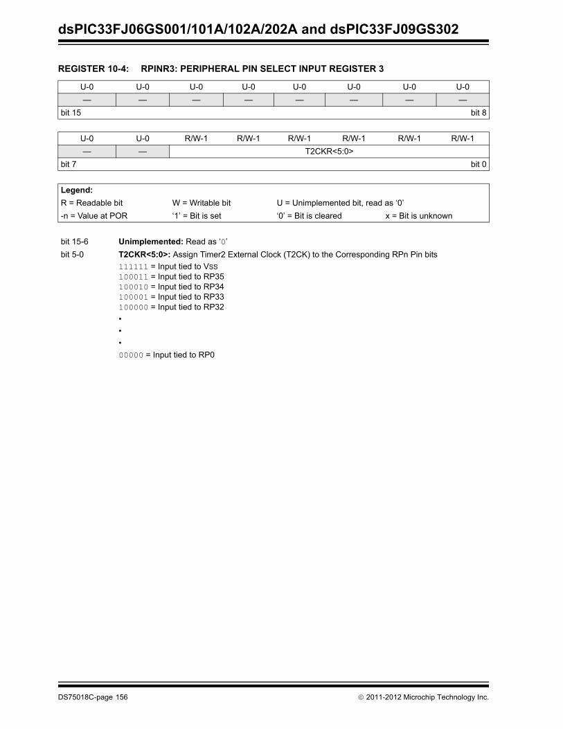
dsPIC33FJ06GS001/101A/102A/202A and dsPIC33FJ09GS302
REGISTER 10-4: RPINR3: PERIPHERAL PIN SELECT INPUT REGISTER 3
U-0 U-0 U-0 U-0 U-0 U-0 U-0 U-0
— — — — — — — —
bit 15 bit 8
U-0 U-0 R/W-1 R/W-1 R/W-1 R/W-1 R/W-1 R/W-1
— — T2CKR<5:0>
bit 7 bit 0
Legend:
R = Readable bit W = Writable bit U = Unimplemented bit, read as ‘0’
-n = Value at POR ‘1’ = Bit is set ‘0’ = Bit is cleared x = Bit is unknown
bit 15-6 Unimplemented: Read as ‘0’
bit 5-0 T2CKR<5:0>: Assign Timer2 External Clock (T2CK) to the Corresponding RPn Pin bits
111111 = Input tied to VSS
100011 = Input tied to RP35100010 = Input tied to RP34100001 = Input tied to RP33100000 = Input tied to RP32
•
•
•
00000 = Input tied to RP0
DS75018C-page 156 2011-2012 Microchip Technology Inc.

dsPIC33FJ06GS001/101A/102A/202A and dsPIC33FJ09GS302
REGISTER 10-5: RPINR7: PERIPHERAL PIN SELECT INPUT REGISTER 7
U-0 U-0 U-0 U-0 U-0 U-0 U-0 U-0
— — — — — — — —
bit 15 bit 8
U-0 U-0 R/W-1 R/W-1 R/W-1 R/W-1 R/W-1 R/W-1
— — IC1R<5:0>(1)
bit 7 bit 0
Legend:
R = Readable bit W = Writable bit U = Unimplemented bit, read as ‘0’
-n = Value at POR ‘1’ = Bit is set ‘0’ = Bit is cleared x = Bit is unknown
bit 15-6 Unimplemented: Read as ‘0’
bit 5-0 IC1R<5:0>: Assign Input Capture 1 (IC1) to the Corresponding RPn Pin bits(1)
111111 = Input tied to VSS
100011 = Input tied to RP35100010 = Input tied to RP34100001 = Input tied to RP33100000 = Input tied to RP32
•
•
•
00000 = Input tied to RP0
Note 1: These bits are not implemented in dsPIC33FJ06GS001/101A/102A devices.
2011-2012 Microchip Technology Inc. DS75018C-page 157
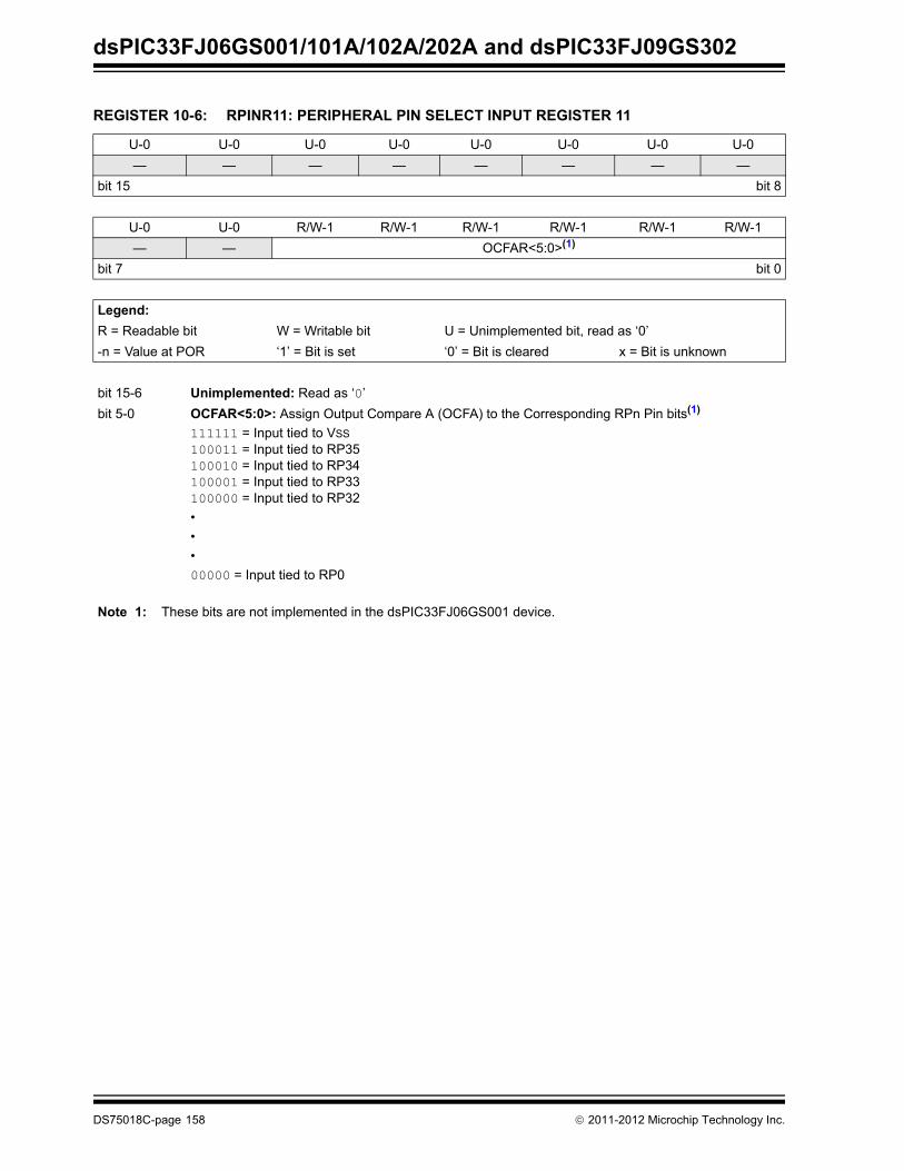
dsPIC33FJ06GS001/101A/102A/202A and dsPIC33FJ09GS302
REGISTER 10-6: RPINR11: PERIPHERAL PIN SELECT INPUT REGISTER 11
U-0 U-0 U-0 U-0 U-0 U-0 U-0 U-0
— — — — — — — —
bit 15 bit 8
U-0 U-0 R/W-1 R/W-1 R/W-1 R/W-1 R/W-1 R/W-1
— — OCFAR<5:0>(1)
bit 7 bit 0
Legend:
R = Readable bit W = Writable bit U = Unimplemented bit, read as ‘0’
-n = Value at POR ‘1’ = Bit is set ‘0’ = Bit is cleared x = Bit is unknown
bit 15-6 Unimplemented: Read as ‘0’
bit 5-0 OCFAR<5:0>: Assign Output Compare A (OCFA) to the Corresponding RPn Pin bits(1)
111111 = Input tied to VSS
100011 = Input tied to RP35100010 = Input tied to RP34100001 = Input tied to RP33100000 = Input tied to RP32
•
•
•
00000 = Input tied to RP0
Note 1: These bits are not implemented in the dsPIC33FJ06GS001 device.
DS75018C-page 158 2011-2012 Microchip Technology Inc.

dsPIC33FJ06GS001/101A/102A/202A and dsPIC33FJ09GS302
REGISTER 10-7: RPINR18: PERIPHERAL PIN SELECT INPUT REGISTER 18
U-0 U-0 R/W-1 R/W-1 R/W-1 R/W-1 R/W-1 R/W-1
— — U1CTSR<5:0>(1)
bit 15 bit 8
U-0 U-0 R/W-1 R/W-1 R/W-1 R/W-1 R/W-1 R/W-1
— — U1RXR<5:0>(1)
bit 7 bit 0
Legend:
R = Readable bit W = Writable bit U = Unimplemented bit, read as ‘0’
-n = Value at POR ‘1’ = Bit is set ‘0’ = Bit is cleared x = Bit is unknown
bit 15-14 Unimplemented: Read as ‘0’
bit 13-8 U1CTSR<5:0>: Assign UART1 Clear-to-Send (U1CTS) to the Corresponding RPn Pin bits(1)
111111 = Input tied to VSS
100011 = Input tied to RP35100010 = Input tied to RP34100001 = Input tied to RP33100000 = Input tied to RP32
•
•
•
00000 = Input tied to RP0
bit 7-6 Unimplemented: Read as ‘0’
bit 5-0 U1RXR<5:0>: Assign UART1 Receive (U1RX) to the Corresponding RPn Pin bits(1)
111111 = Input tied to VSS
100011 = Input tied to RP35100010 = Input tied to RP34100001 = Input tied to RP33100000 = Input tied to RP32
•
•
•
00000 = Input tied to RP0
Note 1: These bits are not implemented in the dsPIC33FJ06GS001 device.
2011-2012 Microchip Technology Inc. DS75018C-page 159

dsPIC33FJ06GS001/101A/102A/202A and dsPIC33FJ09GS302
REGISTER 10-8: RPINR20: PERIPHERAL PIN SELECT INPUT REGISTER 20
U-0 U-0 R/W-1 R/W-1 R/W-1 R/W-1 R/W-1 R/W-1
— — SCK1R<5:0>(1)
bit 15 bit 8
U-0 U-0 R/W-1 R/W-1 R/W-1 R/W-1 R/W-1 R/W-1
— — SDI1R<5:0>(1)
bit 7 bit 0
Legend:
R = Readable bit W = Writable bit U = Unimplemented bit, read as ‘0’
-n = Value at POR ‘1’ = Bit is set ‘0’ = Bit is cleared x = Bit is unknown
bit 15-14 Unimplemented: Read as ‘0’
bit 13-8 SCK1R<5:0>: Assign SPI1 Clock Input (SCK1) to the Corresponding RPn Pin bits(1)
111111 = Input tied to VSS
100011 = Input tied to RP35100010 = Input tied to RP34100001 = Input tied to RP33100000 = Input tied to RP32
•
•
•
00000 = Input tied to RP0
bit 7-6 Unimplemented: Read as ‘0’
bit 5-0 SDI1R<5:0>: Assign SPI1 Data Input (SDI1) to the Corresponding RPn Pin bits(1)
111111 = Input tied to VSS
100011 = Input tied to RP35100010 = Input tied to RP34100001 = Input tied to RP33100000 = Input tied to RP32
•
•
•
00000 = Input tied to RP0
Note 1: These bits are not implemented in the dsPIC33FJ06GS001 device.
DS75018C-page 160 2011-2012 Microchip Technology Inc.
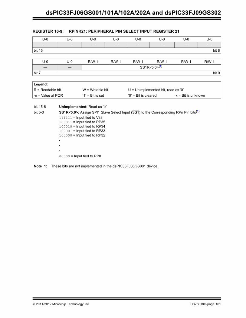
dsPIC33FJ06GS001/101A/102A/202A and dsPIC33FJ09GS302
REGISTER 10-9: RPINR21: PERIPHERAL PIN SELECT INPUT REGISTER 21
U-0 U-0 U-0 U-0 U-0 U-0 U-0 U-0
— — — — — — — —
bit 15 bit 8
U-0 U-0 R/W-1 R/W-1 R/W-1 R/W-1 R/W-1 R/W-1
— — SS1R<5:0>(1)
bit 7 bit 0
Legend:
R = Readable bit W = Writable bit U = Unimplemented bit, read as ‘0’
-n = Value at POR ‘1’ = Bit is set ‘0’ = Bit is cleared x = Bit is unknown
bit 15-6 Unimplemented: Read as ‘0’
bit 5-0 SS1R<5:0>: Assign SPI1 Slave Select Input (SS1) to the Corresponding RPn Pin bits(1)
111111 = Input tied to VSS
100011 = Input tied to RP35100010 = Input tied to RP34100001 = Input tied to RP33100000 = Input tied to RP32
•
•
•
00000 = Input tied to RP0
Note 1: These bits are not implemented in the dsPIC33FJ06GS001 device.
2011-2012 Microchip Technology Inc. DS75018C-page 161

dsPIC33FJ06GS001/101A/102A/202A and dsPIC33FJ09GS302
REGISTER 10-10: RPINR29: PERIPHERAL PIN SELECT INPUT REGISTER 29
U-0 U-0 R/W-1 R/W-1 R/W-1 R/W-1 R/W-1 R/W-1
— — FLT1R<5:0>
bit 15 bit 8
U-0 U-0 U-0 U-0 U-0 U-0 U-0 U-0
— — — — — — — —
bit 7 bit 0
Legend:
R = Readable bit W = Writable bit U = Unimplemented bit, read as ‘0’
-n = Value at POR ‘1’ = Bit is set ‘0’ = Bit is cleared x = Bit is unknown
bit 15-14 Unimplemented: Read as ‘0’
bit 13-8 FLT1R<5:0>: Assign PWM Fault Input 1 (FLT1) to the Corresponding RPn Pin bits
111111 = Input tied to VSS
100011 = Input tied to RP35100010 = Input tied to RP34100001 = Input tied to RP33100000 = Input tied to RP32
•
•
•
00000 = Input tied to RP0
bit 7-0 Unimplemented: Read as ‘0’
DS75018C-page 162 2011-2012 Microchip Technology Inc.

dsPIC33FJ06GS001/101A/102A/202A and dsPIC33FJ09GS302
REGISTER 10-11: RPINR30: PERIPHERAL PIN SELECT INPUT REGISTER 30
U-0 U-0 R/W-1 R/W-1 R/W-1 R/W-1 R/W-1 R/W-1
— — FLT3R<5:0>
bit 15 bit 8
U-0 U-0 R/W-1 R/W-1 R/W-1 R/W-1 R/W-1 R/W-1
— — FLT2R<5:0>
bit 7 bit 0
Legend:
R = Readable bit W = Writable bit U = Unimplemented bit, read as ‘0’
-n = Value at POR ‘1’ = Bit is set ‘0’ = Bit is cleared x = Bit is unknown
bit 15-14 Unimplemented: Read as ‘0’
bit 13-8 FLT3R<5:0>: Assign PWM Fault Input 3 (FLT3) to the Corresponding RPn Pin bits
111111 = Input tied to VSS
100011 = Input tied to RP35100010 = Input tied to RP34100001 = Input tied to RP33100000 = Input tied to RP32
•
•
•
00000 = Input tied to RP0
bit 7-6 Unimplemented: Read as ‘0’
bit 5-0 FLT2R<5:0>: Assign PWM Fault Input 2 (FLT2) to the Corresponding RPn Pin bits
111111 = Input tied to VSS
100011 = Input tied to RP35100010 = Input tied to RP34100001 = Input tied to RP33100000 = Input tied to RP32
•
•
•
00000 = Input tied to RP0
2011-2012 Microchip Technology Inc. DS75018C-page 163

dsPIC33FJ06GS001/101A/102A/202A and dsPIC33FJ09GS302
REGISTER 10-12: RPINR31: PERIPHERAL PIN SELECT INPUT REGISTER 31
U-0 U-0 R/W-1 R/W-1 R/W-1 R/W-1 R/W-1 R/W-1
— — FLT5R<5:0>
bit 15 bit 8
U-0 U-0 R/W-1 R/W-1 R/W-1 R/W-1 R/W-1 R/W-1
— — FLT4R<5:0>
bit 7 bit 0
Legend:
R = Readable bit W = Writable bit U = Unimplemented bit, read as ‘0’
-n = Value at POR ‘1’ = Bit is set ‘0’ = Bit is cleared x = Bit is unknown
bit 15-14 Unimplemented: Read as ‘0’
bit 13-8 FLT5R<5:0>: Assign PWM Fault Input 5 (FLT5) to the Corresponding RPn Pin bits
111111 = Input tied to VSS
100011 = Input tied to RP35100010 = Input tied to RP34100001 = Input tied to RP33100000 = Input tied to RP32
•
•
•
00000 = Input tied to RP0
bit 7-6 Unimplemented: Read as ‘0’
bit 5-0 FLT4R<5:0>: Assign PWM Fault Input 4 (FLT4) to the Corresponding RPn Pin bits
111111 = Input tied to VSS
100011 = Input tied to RP35100010 = Input tied to RP34100001 = Input tied to RP33100000 = Input tied to RP32
•
•
•
00000 = Input tied to RP0
DS75018C-page 164 2011-2012 Microchip Technology Inc.

dsPIC33FJ06GS001/101A/102A/202A and dsPIC33FJ09GS302
REGISTER 10-13: RPINR32: PERIPHERAL PIN SELECT INPUT REGISTER 32
U-0 U-0 R/W-1 R/W-1 R/W-1 R/W-1 R/W-1 R/W-1
— — FLT7R<5:0>
bit 15 bit 8
U-0 U-0 R/W-1 R/W-1 R/W-1 R/W-1 R/W-1 R/W-1
— — FLT6R<5:0>
bit 7 bit 0
Legend:
R = Readable bit W = Writable bit U = Unimplemented bit, read as ‘0’
-n = Value at POR ‘1’ = Bit is set ‘0’ = Bit is cleared x = Bit is unknown
bit 15-14 Unimplemented: Read as ‘0’
bit 13-8 FLT7R<5:0>: Assign PWM Fault Input 7 (FLT7) to the Corresponding RPn Pin bits
111111 = Input tied to VSS
100011 = Input tied to RP35100010 = Input tied to RP34100001 = Input tied to RP33100000 = Input tied to RP32
•
•
•
00000 = Input tied to RP0
bit 7-6 Unimplemented: Read as ‘0’
bit 5-0 FLT6R<5:0>: Assign PWM Fault Input 6 (FLT6) to the Corresponding RPn Pin bits
111111 = Input tied to VSS
100011 = Input tied to RP35100010 = Input tied to RP34100001 = Input tied to RP33100000 = Input tied to RP32
•
•
•
00000 = Input tied to RP0
2011-2012 Microchip Technology Inc. DS75018C-page 165

dsPIC33FJ06GS001/101A/102A/202A and dsPIC33FJ09GS302
REGISTER 10-14: RPINR33: PERIPHERAL PIN SELECT INPUT REGISTER 33
U-0 U-0 R/W-1 R/W-1 R/W-1 R/W-1 R/W-1 R/W-1
— — SYNCI1R<5:0>
bit 15 bit 8
U-0 U-0 R/W-1 R/W-1 R/W-1 R/W-1 R/W-1 R/W-1
— — FLT8R<5:0>
bit 7 bit 0
Legend:
R = Readable bit W = Writable bit U = Unimplemented bit, read as ‘0’
-n = Value at POR ‘1’ = Bit is set ‘0’ = Bit is cleared x = Bit is unknown
bit 15-14 Unimplemented: Read as ‘0’
bit 13-8 SYNCI1R<5:0>: Assign PWM Master Time Base External Synchronization Signal to the Corresponding RPn Pin bits
111111 = Input tied to VSS
100011 = Input tied to RP35100010 = Input tied to RP34100001 = Input tied to RP33100000 = Input tied to RP32
•
•
•
00000 = Input tied to RP0
bit 7-6 Unimplemented: Read as ‘0’
bit 5-0 FLT8R<5:0>: Assign PWM Fault Input 8 (FLT8) to the Corresponding RPn Pin bits
111111 = Input tied to VSS
100011 = Input tied to RP35100010 = Input tied to RP34100001 = Input tied to RP33100000 = Input tied to RP32
•
•
•
00000 = Input tied to RP0
DS75018C-page 166 2011-2012 Microchip Technology Inc.

dsPIC33FJ06GS001/101A/102A/202A and dsPIC33FJ09GS302
REGISTER 10-15: RPINR34: PERIPHERAL PIN SELECT INPUT REGISTER 34
U-0 U-0 U-0 U-0 U-0 U-0 U-0 U-0
— — — — — — — —
bit 15 bit 8
U-0 U-0 R/W-1 R/W-1 R/W-1 R/W-1 R/W-1 R/W-1
— — SYNCI2R<5:0>
bit 7 bit 0
Legend:
R = Readable bit W = Writable bit U = Unimplemented bit, read as ‘0’
-n = Value at POR ‘1’ = Bit is set ‘0’ = Bit is cleared x = Bit is unknown
bit 15-6 Unimplemented: Read as ‘0’
bit 5-0 SYNCI2R<5:0>: Assign PWM Master Time Base External Synchronization Signal to the Corresponding RPn Pin bits
111111 = Input tied to VSS
100011 = Input tied to RP35100010 = Input tied to RP34100001 = Input tied to RP33100000 = Input tied to RP32
•
•
•
00000 = Input tied to RP0
2011-2012 Microchip Technology Inc. DS75018C-page 167

dsPIC33FJ06GS001/101A/102A/202A and dsPIC33FJ09GS302
REGISTER 10-16: RPOR0: PERIPHERAL PIN SELECT OUTPUT REGISTER 0
U-0 U-0 R/W-0 R/W-0 R/W-0 R/W-0 R/W-0 R/W-0
— — RP1R<5:0>
bit 15 bit 8
U-0 U-0 R/W-0 R/W-0 R/W-0 R/W-0 R/W-0 R/W-0
— — RP0R<5:0>
bit 7 bit 0
Legend:
R = Readable bit W = Writable bit U = Unimplemented bit, read as ‘0’
-n = Value at POR ‘1’ = Bit is set ‘0’ = Bit is cleared x = Bit is unknown
bit 15-14 Unimplemented: Read as ‘0’
bit 13-8 RP1R<5:0>: Peripheral Output Function is Assigned to RP1 Output Pin bits
(see Table 10-2 for peripheral function numbers)
bit 7-6 Unimplemented: Read as ‘0’
bit 5-0 RP0R<5:0>: Peripheral Output Function is Assigned to RP0 Output Pin bits
(see Table 10-2 for peripheral function numbers)
REGISTER 10-17: RPOR1: PERIPHERAL PIN SELECT OUTPUT REGISTER 1
U-0 U-0 R/W-0 R/W-0 R/W-0 R/W-0 R/W-0 R/W-0
— — RP3R<5:0>
bit 15 bit 8
U-0 U-0 R/W-0 R/W-0 R/W-0 R/W-0 R/W-0 R/W-0
— — RP2R<5:0>
bit 7 bit 0
Legend:
R = Readable bit W = Writable bit U = Unimplemented bit, read as ‘0’
-n = Value at POR ‘1’ = Bit is set ‘0’ = Bit is cleared x = Bit is unknown
bit 15-14 Unimplemented: Read as ‘0’
bit 13-8 RP3R<5:0>: Peripheral Output Function is Assigned to RP3 Output Pin bits
(see Table 10-2 for peripheral function numbers)
bit 7-6 Unimplemented: Read as ‘0’
bit 5-0 RP2R<5:0>: Peripheral Output Function is Assigned to RP2 Output Pin bits
(see Table 10-2 for peripheral function numbers)
DS75018C-page 168 2011-2012 Microchip Technology Inc.

dsPIC33FJ06GS001/101A/102A/202A and dsPIC33FJ09GS302
REGISTER 10-18: RPOR2: PERIPHERAL PIN SELECT OUTPUT REGISTER 2
U-0 U-0 R/W-0 R/W-0 R/W-0 R/W-0 R/W-0 R/W-0
— — RP5R<5:0>
bit 15 bit 8
U-0 U-0 R/W-0 R/W-0 R/W-0 R/W-0 R/W-0 R/W-0
— — RP4R<5:0>
bit 7 bit 0
Legend:
R = Readable bit W = Writable bit U = Unimplemented bit, read as ‘0’
-n = Value at POR ‘1’ = Bit is set ‘0’ = Bit is cleared x = Bit is unknown
bit 15-14 Unimplemented: Read as ‘0’
bit 13-8 RP5R<5:0>: Peripheral Output Function is Assigned to RP5 Output Pin bits
(see Table 10-2 for peripheral function numbers)
bit 7-6 Unimplemented: Read as ‘0’
bit 5-0 RP4R<5:0>: Peripheral Output Function is Assigned to RP4 Output Pin bits
(see Table 10-2 for peripheral function numbers)
REGISTER 10-19: RPOR3: PERIPHERAL PIN SELECT OUTPUT REGISTER 3
U-0 U-0 R/W-0 R/W-0 R/W-0 R/W-0 R/W-0 R/W-0
— — RP7R<5:0>
bit 15 bit 8
U-0 U-0 R/W-0 R/W-0 R/W-0 R/W-0 R/W-0 R/W-0
— — RP6R<5:0>
bit 7 bit 0
Legend:
R = Readable bit W = Writable bit U = Unimplemented bit, read as ‘0’
-n = Value at POR ‘1’ = Bit is set ‘0’ = Bit is cleared x = Bit is unknown
bit 15-14 Unimplemented: Read as ‘0’
bit 13-8 RP7R<5:0>: Peripheral Output Function is Assigned to RP7 Output Pin bits
(see Table 10-2 for peripheral function numbers)
bit 7-6 Unimplemented: Read as ‘0’
bit 5-0 RP6R<5:0>: Peripheral Output Function is Assigned to RP6 Output Pin bits
(see Table 10-2 for peripheral function numbers)
2011-2012 Microchip Technology Inc. DS75018C-page 169

dsPIC33FJ06GS001/101A/102A/202A and dsPIC33FJ09GS302
REGISTER 10-20: RPOR4: PERIPHERAL PIN SELECT OUTPUT REGISTER 4
U-0 U-0 R/W-0 R/W-0 R/W-0 R/W-0 R/W-0 R/W-0
— — RP9R<5:0>(1)
bit 15 bit 8
U-0 U-0 R/W-0 R/W-0 R/W-0 R/W-0 R/W-0 R/W-0
— — RP8R<5:0>(1)
bit 7 bit 0
Legend:
R = Readable bit W = Writable bit U = Unimplemented bit, read as ‘0’
-n = Value at POR ‘1’ = Bit is set ‘0’ = Bit is cleared x = Bit is unknown
bit 15-14 Unimplemented: Read as ‘0’
bit 13-8 RP9R<5:0>: Peripheral Output Function is Assigned to RP9 Output Pin bits(1)
(see Table 10-2 for peripheral function numbers)
bit 7-6 Unimplemented: Read as ‘0’
bit 5-0 RP8R<5:0>: Peripheral Output Function is Assigned to RP8 Output Pin bits(1)
(see Table 10-2 for peripheral function numbers)
Note 1: These bits are not implemented in dsPIC33FJ06GS001/101A devices.
REGISTER 10-21: RPOR5: PERIPHERAL PIN SELECT OUTPUT REGISTER 5
U-0 U-0 R/W-0 R/W-0 R/W-0 R/W-0 R/W-0 R/W-0
— — RP11R<5:0>(1)
bit 15 bit 8
U-0 U-0 R/W-0 R/W-0 R/W-0 R/W-0 R/W-0 R/W-0
— — RP10R<5:0>(1)
bit 7 bit 0
Legend:
R = Readable bit W = Writable bit U = Unimplemented bit, read as ‘0’
-n = Value at POR ‘1’ = Bit is set ‘0’ = Bit is cleared x = Bit is unknown
bit 15-14 Unimplemented: Read as ‘0’
bit 13-8 RP11R<5:0>: Peripheral Output Function is Assigned to RP11 Output Pin bits(1)
(see Table 10-2 for peripheral function numbers)
bit 7-6 Unimplemented: Read as ‘0’
bit 5-0 RP10R<5:0>: Peripheral Output Function is Assigned to RP10 Output Pin bits(1)
(see Table 10-2 for peripheral function numbers)
Note 1: These bits are not implemented in dsPIC33FJ06GS001/101A devices.
DS75018C-page 170 2011-2012 Microchip Technology Inc.

dsPIC33FJ06GS001/101A/102A/202A and dsPIC33FJ09GS302
REGISTER 10-22: RPOR6: PERIPHERAL PIN SELECT OUTPUT REGISTER 6
U-0 U-0 R/W-0 R/W-0 R/W-0 R/W-0 R/W-0 R/W-0
— — RP13R<5:0>(1)
bit 15 bit 8
U-0 U-0 R/W-0 R/W-0 R/W-0 R/W-0 R/W-0 R/W-0
— — RP12R<5:0>(1)
bit 7 bit 0
Legend:
R = Readable bit W = Writable bit U = Unimplemented bit, read as ‘0’
-n = Value at POR ‘1’ = Bit is set ‘0’ = Bit is cleared x = Bit is unknown
bit 15-14 Unimplemented: Read as ‘0’
bit 13-8 RP13R<5:0>: Peripheral Output Function is Assigned to RP13 Output Pin bits(1)
(see Table 10-2 for peripheral function numbers)
bit 7-6 Unimplemented: Read as ‘0’
bit 5-0 RP12R<5:0>: Peripheral Output Function is Assigned to RP12 Output Pin bits(1)
(see Table 10-2 for peripheral function numbers)
Note 1: These bits are not implemented in dsPIC33FJ06GS001/101A devices.
REGISTER 10-23: RPOR7: PERIPHERAL PIN SELECT OUTPUT REGISTER 7
U-0 U-0 R/W-0 R/W-0 R/W-0 R/W-0 R/W-0 R/W-0
— — RP15R<5:0>(1)
bit 15 bit 8
U-0 U-0 R/W-0 R/W-0 R/W-0 R/W-0 R/W-0 R/W-0
— — RP14R<5:0>(1)
bit 7 bit 0
Legend:
R = Readable bit W = Writable bit U = Unimplemented bit, read as ‘0’
-n = Value at POR ‘1’ = Bit is set ‘0’ = Bit is cleared x = Bit is unknown
bit 15-14 Unimplemented: Read as ‘0’
bit 13-8 RP15R<5:0>: Peripheral Output Function is Assigned to RP15 Output Pin bits(1)
(see Table 10-2 for peripheral function numbers)
bit 7-6 Unimplemented: Read as ‘0’
bit 5-0 RP14R<5:0>: Peripheral Output Function is Assigned to RP14 Output Pin bits(1)
(see Table 10-2 for peripheral function numbers)
Note 1: These bits are not implemented in dsPIC33FJ06GS001/101A devices.
2011-2012 Microchip Technology Inc. DS75018C-page 171

dsPIC33FJ06GS001/101A/102A/202A and dsPIC33FJ09GS302
REGISTER 10-24: RPOR16: PERIPHERAL PIN SELECT OUTPUT REGISTER 16
REGISTER 10-25: RPOR17: PERIPHERAL PIN SELECT OUTPUT REGISTER 17
U-0 U-0 R/W-0 R/W-0 R/W-0 R/W-0 R/W-0 R/W-0
— — RP33R<5:0>
bit 15 bit 8
U-0 U-0 R/W-0 R/W-0 R/W-0 R/W-0 R/W-0 R/W-0
— — RP32R<5:0>
bit 7 bit 0
Legend:
R = Readable bit W = Writable bit U = Unimplemented bit, read as ‘0’
-n = Value at POR ‘1’ = Bit is set ‘0’ = Bit is cleared x = Bit is unknown
bit 15-14 Unimplemented: Read as ‘0’
bit 13-8 RP33R<5:0>: Peripheral Output Function is Assigned to RP33 Output Pin bits
(see Table 10-2 for peripheral function numbers)
bit 7-6 Unimplemented: Read as ‘0’
bit 5-0 RP32R<5:0>: Peripheral Output Function is Assigned to RP32 Output Pin bits
(see Table 10-2 for peripheral function numbers)
U-0 U-0 R/W-0 R/W-0 R/W-0 R/W-0 R/W-0 R/W-0
— — RP35R<5:0>
bit 15 bit 8
U-0 U-0 R/W-0 R/W-0 R/W-0 R/W-0 R/W-0 R/W-0
— — RP34R<5:0>
bit 7 bit 0
Legend:
R = Readable bit W = Writable bit U = Unimplemented bit, read as ‘0’
-n = Value at POR ‘1’ = Bit is set ‘0’ = Bit is cleared x = Bit is unknown
bit 15-14 Unimplemented: Read as ‘0’
bit 13-8 RP35R<5:0>: Peripheral Output Function is Assigned to RP35 Output Pin bits
(see Table 10-2 for peripheral function numbers)
bit 7-6 Unimplemented: Read as ‘0’
bit 5-0 RP34R<5:0>: Peripheral Output Function is Assigned to RP34 Output Pin bits
(see Table 10-2 for peripheral function numbers)
DS75018C-page 172 2011-2012 Microchip Technology Inc.

dsPIC33FJ06GS001/101A/102A/202A and dsPIC33FJ09GS302
11.0 TIMER1
The Timer1 module is a 16-bit timer, which can serveas a time counter for the Real-Time Clock (RTC) oroperate as a free-running interval timer/counter.
The Timer1 module has the following unique featuresover other timers:
• Can be operated from the low-power 32 kHz crystal oscillator available on the device
• Can be operated in Asynchronous Counter mode from an external clock source
• The Timer1 External Clock Input (T1CK) can optionally be synchronized to the internal device clock and the clock synchronization is performed after the prescaler
The unique features of Timer1 allow it to be used forReal-Time Clock applications. A block diagram ofTimer1 is shown in Figure 11-1.
The Timer1 module can operate in one of the followingmodes:
• Timer mode
• Gated Timer mode
• Synchronous Counter mode
• Asynchronous Counter mode
In Timer and Gated Timer modes, the input clock isderived from the internal instruction cycle clock (FCY).In Synchronous and Asynchronous Counter modes,the input clock is derived from the external clock inputat the T1CK pin.
The Timer1 modes are determined by the following bits:
• Timer1 Clock Source Control bit: TCS (T1CON<1>)
• Timer1 Synchronization Control bit: TSYNC (T1CON<2>)
• Timer1 Gate Control bit: TGATE (T1CON<6>)
The Timer1 control bit settings for different operatingmodes are given in the Table 11-1.
TABLE 11-1: TIMER1 MODE SETTINGS
FIGURE 11-1: 16-BIT TIMER1 MODULE BLOCK DIAGRAM
Note 1: This data sheet summarizes the featuresof the dsPIC33FJ06GS001/101A/102A/202A and dsPIC33FJ09GS302 familiesof devices. It is not intended to be acomprehensive reference source. Tocomplement the information in this datasheet, refer to Section 11. “Timers”(DS70205) in the “dsPIC33F/PIC24HFamily Reference Manual”, which isavailable from the Microchip web site(www.microchip.com).
2: Some registers and associated bitsdescribed in this section may not beavailable on all devices. Refer toSection 4.0 “Memory Organization” inthis data sheet for device-specific registerand bit information.
Mode TCS TGATE TSYNC
Timer1 0 0 x
Gated Timer1 0 1 x
Synchronous Counter
1 x 1
Asynchronous Counter
1 x 0
TGATE
TCS
00
10
x1
Comparator
PR1
TGATE
Set T1IF Flag
0
1
TSYNC
1
0
SyncEqual
Reset
T1CKPrescaler
(/n)
TCKPS<1:0>
FP
Falling EdgeDetect
Prescaler(/n)
TCKPS<1:0>
GateSync
TMR1
2011-2012 Microchip Technology Inc. DS75018C-page 173

dsPIC33FJ06GS001/101A/102A/202A and dsPIC33FJ09GS302
11.1 Timer1 Control Register
REGISTER 11-1: T1CON: TIMER1 CONTROL REGISTER
R/W-0 U-0 R/W-0 U-0 U-0 U-0 U-0 U-0
TON — TSIDL — — — — —
bit 15 bit 8
U-0 R/W-0 R/W-0 R/W-0 U-0 R/W-0 R/W-0 U-0
— TGATE TCKPS<1:0> — TSYNC TCS —
bit 7 bit 0
Legend:
R = Readable bit W = Writable bit U = Unimplemented bit, read as ‘0’
-n = Value at POR ‘1’ = Bit is set ‘0’ = Bit is cleared x = Bit is unknown
bit 15 TON: Timer1 On bit
1 = Starts 16-bit Timer10 = Stops 16-bit Timer1
bit 14 Unimplemented: Read as ‘0’
bit 13 TSIDL: Stop in Idle Mode bit
1 = Discontinues module operation when device enters Idle mode0 = Continues module operation in Idle mode
bit 12-7 Unimplemented: Read as ‘0’
bit 6 TGATE: Timer1 Gated Time Accumulation Enable bit
When TCS = 1: This bit is ignored.
When TCS = 0: 1 = Gated time accumulation is enabled0 = Gated time accumulation is disabled
bit 5-4 TCKPS<1:0>: Timer1 Input Clock Prescale Select bits
11 = 1:256 10 = 1:6401 = 1:8 00 = 1:1
bit 3 Unimplemented: Read as ‘0’
bit 2 TSYNC: Timer1 External Clock Input Synchronization Select bit
When TCS = 1: 1 = Synchronizes external clock input0 = Does not synchronize external clock input
When TCS = 0: This bit is ignored.
bit 1 TCS: Timer1 Clock Source Select bit
1 = External clock from T1CK pin (on the rising edge) 0 = Internal clock (FCY)
bit 0 Unimplemented: Read as ‘0’
DS75018C-page 174 2011-2012 Microchip Technology Inc.

dsPIC33FJ06GS001/101A/102A/202A and dsPIC33FJ09GS302
12.0 TIMER2 FEATURES
Timer2 is a Type B timer with an external clock input(TxCK) that is always synchronized to the internaldevice clock and the clock synchronization isperformed after the prescaler.
The Timer2 module can operate in one of the followingmodes:
• Timer mode
• Gated Timer mode
• Synchronous Counter mode
In Timer and Gated Timer modes, the input clock isderived from the internal instruction cycle clock (FCY).In Synchronous Counter mode, the input clock isderived from the external clock input at the TxCK pin.
The Timer modes are determined by the following bits:
• TCS (TxCON<1>): Timer Clock Source Control bit
• TGATE (TxCON<6>): Timer Gate Control bit
The Timer control bit settings for different operatingmodes are given in Table 12-1.
TABLE 12-1: TIMER MODE SETTINGS
12.1 16-Bit Operation
To configure any of the timers for individual 16-bitoperation:
1. Select the timer prescaler ratio using theTCKPS<1:0> bits.
2. Set the Clock and Gating modes using the TCSand TGATE bits.
3. Load the Timer Period value into the PRxregister.
4. If interrupts are required, set the Timerx InterruptEnable bit, TxIE. Use the priority bits,TxIP<2:0>, to set the interrupt priority.
5. Set the TON bit.
FIGURE 12-1: TYPE B TIMER BLOCK DIAGRAM (x = 2)
Note 1: This data sheet summarizes the featuresof the dsPIC33FJ06GS001/101A/102A/202A and dsPIC33FJ09GS302 familiesof devices. It is not intended to be acomprehensive reference source. Tocomplement the information in this datasheet, refer to Section 11. “Timers”(DS70205) in the “dsPIC33F/PIC24HFamily Reference Manual”, which isavailable on the Microchip web site(www.microchip.com).
2: Some registers and associated bitsdescribed in this section may not beavailable on all devices. Refer toSection 4.0 “Memory Organization” inthis data sheet for device-specific registerand bit information.
Mode TCS TGATE
Timer 0 0
Gated Timer 0 1
Synchronous Counter 1 x
Prescaler(/n)
TGATE
TCS
00
10
x1
TMRx
Comparator
PRx
TGATE
Set TxIF Flag
0
1
TCKPS<1:0>
Equal
Reset
TxCK
GateSync
FP
Falling EdgeDetect
Prescaler(/n)
TCKPS<1:0>
Sync
2011-2012 Microchip Technology Inc. DS75018C-page 175

dsPIC33FJ06GS001/101A/102A/202A and dsPIC33FJ09GS302
12.2 Timer2 Control Register
REGISTER 12-1: T2CON: TIMER2 CONTROL REGISTER
R/W-0 U-0 R/W-0 U-0 U-0 U-0 U-0 U-0
TON — TSIDL — — — — —
bit 15 bit 8
U-0 R/W-0 R/W-0 R/W-0 U-0 U-0 R/W-0 U-0
— TGATE TCKPS<1:0> — — TCS —
bit 7 bit 0
Legend:
R = Readable bit W = Writable bit U = Unimplemented bit, read as ‘0’
-n = Value at POR ‘1’ = Bit is set ‘0’ = Bit is cleared x = Bit is unknown
bit 15 TON: Timerx On bit
1 = Starts 16-bit timer0 = Stops 16-bit timer
bit 14 Unimplemented: Read as ‘0’
bit 13 TSIDL: Stop in Idle Mode bit
1 = Discontinues timer operation when device enters Idle mode0 = Continues timer operation in Idle mode
bit 12-7 Unimplemented: Read as ‘0’
bit 6 TGATE: Timerx Gated Time Accumulation Enable bit
When TCS = 1:This bit is ignored.
When TCS = 0:1 = Gated time accumulation is enabled0 = Gated time accumulation is disabled
bit 5-4 TCKPS<1:0>: Timerx Input Clock Prescale Select bits
11 = 1:256 prescale value10 = 1:64 prescale value01 = 1:8 prescale value00 = 1:1 prescale value
bit 3-2 Unimplemented: Read as ‘0’
bit 1 TCS: Timerx Clock Source Select bit
1 = External clock from T2CK pin0 = Internal clock (FOSC/2)
bit 0 Unimplemented: Read as ‘0’
DS75018C-page 176 2011-2012 Microchip Technology Inc.

dsPIC33FJ06GS001/101A/102A/202A and dsPIC33FJ09GS302
13.0 INPUT CAPTURE
The input capture module is useful in applicationsrequiring frequency (period) and pulse measurement.
The input capture module captures the 16-bit value ofthe selected Time Base register when an event occursat the IC1 pin. The events that cause a capture eventare listed below in three categories:
• Simple Capture Event modes:
- Capture timer value on every falling edge of input at IC1 pin
- Capture timer value on every rising edge of input at IC1 pin
• Capture timer value on every edge (rising and falling)
• Prescaler Capture Event modes:
- Capture timer value on every 4th rising edge of input at IC1 pin
- Capture timer value on every 16th rising edge of input at IC1 pin
The input capture module uses the Timer2 moduleas its timer; however, it can use either an internal orexternal clock.
Other operational features include:
• Device wake-up from capture pin during CPU Sleep and Idle modes
• Interrupt on input capture event
• 4-word FIFO buffer for capture values:
- Interrupt optionally generated after 1, 2, 3 or 4 buffer locations are filled
• Use of input capture to provide additional sources of external interrupts
FIGURE 13-1: INPUT CAPTURE BLOCK DIAGRAM
Note 1: This data sheet summarizes the featuresof the dsPIC33FJ06GS001/101A/102A/202A and dsPIC33FJ09GS302 familiesof devices. It is not intended to be acomprehensive reference source. Tocomplement the information in this datasheet, refer to Section 12. “Input Cap-ture” (DS70198) in the “dsPIC33F/PIC24H Family Reference Manual”,which is available on the Microchip website (www.microchip.com).
2: Some registers and associated bitsdescribed in this section may not beavailable on all devices. Refer toSection 4.0 “Memory Organization” inthis data sheet for device-specific registerand bit information.
IC1BUF
IC1 PinICM<2:0> (IC1CON<2:0>)
Mode Select3
Set Flag IC1IF(in IFS0 Register)
TMR2
Edge Detection Logic
16
FIFOR/WLogic
ICI<1:0>
ICOV, ICBNE (IC1CON<4:3>)
IC1CONInterrupt
Logic
System Bus
FIF
O
PrescalerCounter(1, 4, 16)
andClock Synchronizer
2011-2012 Microchip Technology Inc. DS75018C-page 177

dsPIC33FJ06GS001/101A/102A/202A and dsPIC33FJ09GS302
13.1 Input Capture Registers
REGISTER 13-1: IC1CON: INPUT CAPTURE 1 CONTROL REGISTER
U-0 U-0 R/W-0 U-0 U-0 U-0 U-0 U-0
— — ICSIDL — — — — —
bit 15 bit 8
R/W-0 R/W-0 R/W-0 R-0, HC R-0, HC R/W-0 R/W-0 R/W-0
ICTMR(1) ICI<1:0> ICOV ICBNE ICM<2:0>
bit 7 bit 0
Legend: HC = Hardware Clearable bit
R = Readable bit W = Writable bit U = Unimplemented bit, read as ‘0’
-n = Value at POR ‘1’ = Bit is set ‘0’ = Bit is cleared x = Bit is unknown
bit 15-14 Unimplemented: Read as ‘0’
bit 13 ICSIDL: Input Capture Module Stop in Idle Control bit
1 = Input capture module halts in CPU Idle mode0 = Input capture module continues to operate in CPU Idle mode
bit 12-8 Unimplemented: Read as ‘0’
bit 7 ICTMR: Input Capture Timer Select bit(1)
1 = TMR2 contents are captured on capture event0 = Reserved
bit 6-5 ICI<1:0>: Select Number of Captures per Interrupt bits
11 = Interrupt on every fourth capture event10 = Interrupt on every third capture event01 = Interrupt on every second capture event00 = Interrupt on every capture event
bit 4 ICOV: Input Capture Overflow Status Flag bit (read-only)
1 = Input capture overflow occurred0 = No input capture overflow occurred
bit 3 ICBNE: Input Capture Buffer Empty Status bit (read-only)
1 = Input capture buffer is not empty, at least one more capture value can be read0 = Input capture buffer is empty
bit 2-0 ICM<2:0>: Input Capture Mode Select bits
111 = Input capture functions as interrupt pin only when device is in Sleep or Idle mode. Rising edgedetect only; all other control bits are not applicable.
110 = Unused (module disabled)101 = Capture mode, every 16th rising edge100 = Capture mode, every 4th rising edge011 = Capture mode, every rising edge010 = Capture mode, every falling edge001 = Capture mode, every edge (rising and falling). ICI<1:0> bits do not control interrupt generation
for this mode.000 = Input capture module is turned off
Note 1: This bit is not available in dsPIC33FJ06GS001/101A/102A devices.
DS75018C-page 178 2011-2012 Microchip Technology Inc.

dsPIC33FJ06GS001/101A/102A/202A and dsPIC33FJ09GS302
14.0 OUTPUT COMPARE
The output compare module can select either Timer1 orTimer2 for its time base. The module compares thevalue of the timer with the value of one or two Compareregisters, depending on the operating mode selected.The state of the output pin changes when the timervalue matches the Output Compare register value. Theoutput compare module generates either a single
output pulse, or a sequence of output pulses, bychanging the state of the output pin on the comparematch events. The output compare module can alsogenerate interrupts on compare match events.
The output compare module has multiple operatingmodes:
• Active-Low One-Shot mode
• Active-High One-Shot mode
• Toggle mode
• Delayed One-Shot mode
• Continuous Pulse mode
• PWM mode without Fault Protection
• PWM mode with Fault Protection
If a Fault condition is detected on the OCFA pin, theoutput pin(s) of the output compare module are placedin tri-state. The user may elect to use a pull-down orpull-up resistor on the PWM pin to provide for a desiredstate if a Fault condition occurs.
FIGURE 14-1: OUTPUT COMPARE MODULE BLOCK DIAGRAM
Note 1: This data sheet summarizes the featuresof the dsPIC33FJ06GS001/101A/102A/202A and dsPIC33FJ09GS302 familiesof devices. It is not intended to be acomprehensive reference source. Tocomplement the information in this datasheet, refer to Section 13. “OutputCompare” (DS70209) in the “dsPIC33F/PIC24H Family Reference Manual”,which is available on the Microchip website (www.microchip.com).
2: Some registers and associated bitsdescribed in this section may not beavailable on all devices. Refer toSection 4.0 “Memory Organization” inthis data sheet for device-specific registerand bit information.
Note: The output compare module is notimplemented in the dsPIC33FJ06GS001device.
OC1R
Comparator
OutputLogic
OCM<2:0>
Output Enable
OC1
Set Flag bit,OC1IF
OC1RS
Mode Select
3
16
OCFA
TMR2
QSR
TMR2Rollover
2011-2012 Microchip Technology Inc. DS75018C-page 179

dsPIC33FJ06GS001/101A/102A/202A and dsPIC33FJ09GS302
14.1 Output Compare Modes
Configure the Output Compare modes by setting theappropriate Output Compare Mode (OCM<2:0>) bits inthe Output Compare Control (OC1CON<2:0>) register.Table 14-1 lists the different bit settings for the OutputCompare modes. Figure 14-2 illustrates the outputcompare operation for various modes. The user
application must disable the associated timer whenwriting to the Output Compare Control registers toavoid malfunctions.
TABLE 14-1: OUTPUT COMPARE MODES
FIGURE 14-2: OUTPUT COMPARE OPERATION
Note: Refer to Section 13. “Output Compare”(DS70209) in the “dsPIC33F/PIC24HFamily Reference Manual” for OC1R andOC1RS register restrictions.
OCM<2:0> Mode OC1 Pin Initial State OC1 Interrupt Generation
000 Module Disabled Controlled by GPIO register —
001 Active-Low One-Shot 0 OC1 rising edge
010 Active-High One-Shot 1 OC1 falling edge
011 Toggle Current output is maintained OC1 rising and falling edge
100 Delayed One-Shot 0 OC1 falling edge
101 Continuous Pulse 0 OC1 falling edge
110 PWM without Fault Protection ‘0’ if OC1R is zero,‘1’ if OC1R is non-zero
No interrupt
111 PWM with Fault Protection ‘0’ if OC1R is zero,‘1’ if OC1R is non-zero
OCFA falling edge for OC1 to OC4
OC1RS
TMRx
OC1R
Timerx is Reset onPeriod Match
Continuous Pulse(OCM<2:0> = 101)
PWM(OCM<2:0> = 110 or 111)
Active-Low One-Shot(OCM<2:0> = 001)
Active-High One-Shot
(OCM<2:0> = 010)
Toggle(OCM<2:0> = 011)
Delayed One-Shot(OCM<2:0> = 100)
Output Compare Mode Enabled
DS75018C-page 180 2011-2012 Microchip Technology Inc.

dsPIC33FJ06GS001/101A/102A/202A and dsPIC33FJ09GS302
14.2 Output Compare Control Registers
REGISTER 14-1: OC1CON: OUTPUT COMPARE 1 CONTROL REGISTER
U-0 U-0 R/W-0 U-0 U-0 U-0 U-0 U-0
— — OCSIDL — — — — —
bit 15 bit 8
U-0 U-0 U-0 R-0, HC U-0 R/W-0 R/W-0 R/W-0
— — — OCFLT — OCM<2:0>
bit 7 bit 0
Legend: HC = Hardware Clearable bit
R = Readable bit W = Writable bit U = Unimplemented bit, read as ‘0’
-n = Value at POR ‘1’ = Bit is set ‘0’ = Bit is cleared x = Bit is unknown
bit 15-14 Unimplemented: Read as ‘0’
bit 13 OCSIDL: Stop Output Compare in Idle Mode Control bit
1 = Output Compare 1 halts in CPU Idle mode0 = Output Compare 1 continues to operate in CPU Idle mode
bit 12-5 Unimplemented: Read as ‘0’
bit 4 OCFLT: PWM Fault Condition Status bit
1 = PWM Fault condition has occurred (cleared in hardware only)0 = No PWM Fault condition has occurred (this bit is only used when OCM<2:0> = 111)
bit 3 Unimplemented: Read as ‘0’
bit 2-0 OCM<2:0>: Output Compare Mode Select bits
111 = PWM mode on OC1, Fault pin is enabled110 = PWM mode on OC1, Fault pin is disabled101 = Initializes OC1 pin low, generates continuous output pulses on OC1 pin100 = Initializes OC1 pin low, generates single output pulse on OC1 pin011 = Compare event toggles OC1 pin010 = Initializes OC1 pin high, compare event forces OC1 pin low001 = Initializes OC1 pin low, compare event forces OC1 pin high 000 = Output compare channel is disabled
2011-2012 Microchip Technology Inc. DS75018C-page 181

dsPIC33FJ06GS001/101A/102A/202A and dsPIC33FJ09GS302
NOTES:
DS75018C-page 182 2011-2012 Microchip Technology Inc.

dsPIC33FJ06GS001/101A/102A/202A and dsPIC33FJ09GS302
15.0 HIGH-SPEED PWM
The high-speed PWM module supports a wide varietyof PWM modes and output formats. This PWM moduleis ideal for power conversion applications, such as:
• AC/DC Converters
• DC/DC Converters
• Power Factor Correction (PFC)
• Uninterruptible Power Supply (UPS)
• Inverters
• Battery Chargers
• Digital Lighting
15.1 Features OverviewThe high-speed PWM module incorporates thefollowing features:
• Two to three PWM generators with four to six outputs
• Individual time base and duty cycle for each of the six PWM outputs
• Dead time for rising and falling edges:
• Duty cycle resolution of 1.04 ns(1,2)
• Dead-time resolution of 1.04 ns(1,2)
• Phase-shift resolution of 1.04 ns(1,2)
• Frequency resolution of 1.04 ns(1,2)
• Supported PWM modes:
- Standard Edge-Aligned
- True Independent Output
- Complementary
- Center-Aligned
- Push-Pull
- Multiphase
- Variable Phase
- Fixed Off Time
- Current Reset
- Current Limit
• Independent Fault/Current-Limit inputs for each of the six PWM outputs
• Output override control
• Special Event Trigger
• PWM capture feature
• Prescaler for input clock
• Dual trigger from PWM to ADC
• PWMxH, PWMxL output pin swapping
• Remappable PWM4H, PWM4L pins
• On-the-fly PWM frequency, duty cycle and phase-shift changes
• Disabling of individual PWM generators to reduce power consumption
• Leading-Edge Blanking (LEB) functionality
• PWM output chopping (see Note 1)
Figure 15-1 conceptualizes the PWM module in asimplified block diagram. Figure 15-2 illustrates howthe module hardware is partitioned for each PWM out-put pair for the Complementary PWM mode. Eachfunctional unit of the PWM module is discussed insubsequent sections.
The PWM module contains three PWM generators.The module has up to six PWM output pins: PWM1H,PWM1L, PWM2H, PWM2L, PWM4H and PWM4L. Forcomplementary outputs, these six I/O pins are groupedinto H/L pairs.
Note 1: This data sheet summarizes the featuresof the dsPIC33FJ06GS001/101A/102A/202A and dsPIC33FJ09GS302 familiesof devices. It is not intended to be acomprehensive reference source. Tocomplement the information in this datasheet, refer to Section 43. “High-SpeedPWM” (DS70323) in the “dsPIC33F/PIC24H Family Reference Manual”,which is available on the Microchip website (www.microchip.com).
2: Some registers and associated bitsdescribed in this section may not beavailable on all devices. Refer toSection 4.0 “Memory Organization” inthis data sheet for device-specific registerand bit information.
Note 1: Resolution is 8.32 ns in Center-AlignedPWM mode.
2: Resolution is 8.32 ns for dsPIC33FJ06GS001 devices.
Note 1: The chopping function performs a logicalAND of the PWM outputs with a veryhigh-frequency clock signal. The chop-ping frequency is typically hundreds orthousands of time higher in frequency, ascompared to the PWM frequency. Chop-ping a PWM signal constrains the use ofa pulse transformer to cross the isolationbarrier.
2011-2012 Microchip Technology Inc. DS75018C-page 183
dsPIC33FJ06GS001/101A/102A/202A and dsPIC33FJ09GS302
15.2 Feature DescriptionThe PWM module is designed for applications thatrequire:
• High-resolution at high PWM frequencies• The ability to drive Standard, Edge-Aligned,
Center-Aligned Complementary mode, and Push-Pull mode outputs
• The ability to create multiphase PWM outputs
For Center-Aligned mode, the duty cycle, period, phaseand dead-time resolutions will be 8.32 ns.
Two common, medium power converter topologies arepush-pull and half-bridge. These designs require thePWM output signal to be switched between alternatepins, as provided by the Push-Pull PWM mode.
A phase-shifted PWM describes the situation whereeach PWM generator provides outputs, but the phaserelationship between the generator outputs isspecifiable and changeable.
A multiphase PWM is often used to improve DC/DCConverter load transient response, and reduce the sizeof output filter capacitors and inductors. Multiple DC/DC Converters are often operated in parallel, butphase-shifted in time. A single PWM output, operatingat 250 kHz, has a period of 4 s, but an array of fourPWM channels staggered by 1 s each, yields aneffective switching frequency of 1 MHz. MultiphasePWM applications typically use a fixed-phaserelationship.
A variable phase PWM is useful in Zero VoltageTransition (ZVT) power converters. Here, the PWMduty cycle is always 50%, and the power flow iscontrolled by varying the relative phase-shift betweenthe two PWM generators.
DS75018C-page 184 2011-2012 Microchip Technology Inc.

dsPIC33FJ06GS001/101A/102A/202A and dsPIC33FJ09GS302
FIGURE 15-1: SIMPLIFIED CONCEPTUAL BLOCK DIAGRAM OF HIGH-SPEED PWM
MUX
Latch
Comparator
Timer
PDC2
Phase
MUX
Latch
Comparator
Timer
PDC4
Phase
MUX
Latch
Comparator
Timer
PDC1
PWMCONx
LEBCONx
Channel 1Dead-Time Generator
PTCON
SEVTCMP
Comparator Special Event
IOCONx
PWM Enable and Mode Control
Channel 4Dead-Time Generator
ALTDTRx, DTRxDead-Time Control
Special EventPostscaler
FLTX(1)
PWM2L
PWM2H
16-B
it D
ata
Bus
PWM1L
PWM1H
FCLCONx
Pin and Mode Control
MDC
ADC Trigger Control
Master Duty Cycle Register
Fault Mode and Pin Control
Pin Override Control
Special Event
PTPER
Timer Period
PWM
PWM
PWM
PTMR
Master Time Base
Phase
Channel 2Dead-Time Generator
PWM4L(1)
PWM4H(1)
PW
M U
ser,
Cu
rre
nt-L
imit
and
Fau
lt O
verr
ide
and
Rou
ting
Lo
gic
Fau
lt C
LM
T O
verr
ide
Lo
gic
Trigger
Comparison Value
Fault Control Logic
TRGCONx
Control for Blanking External Input Signals
SYNCO1(1)
SYNCIX(1)External Time Base
Synchronization
Generator 1
Generator 2(2)
Generator 4(3)
Note 1: These pins are remappable.
2: This PWM generator is not available in dsPIC33FJ06GS001/101A devices.
3: This PWM generator is only available in dsPIC33FJ06GS001/101A and dsPIC33FJ09GS302A devices.
Chop ClockGenerator
CHOP
2011-2012 Microchip Technology Inc. DS75018C-page 185

dsPIC33FJ06GS001/101A/102A/202A and dsPIC33FJ09GS302
FIGURE 15-2: PARTITIONED OUTPUT PAIR, COMPLEMENTARY PWM MODE
15.3 PWM Control Registers
The following registers control the operation of thehigh-speed PWM module.
• PTCON: PWM Time Base Control Register
• PTCON2: PWM Clock Divider Select Register 2
• PTPER: PWM Master Time Base Register(1)
• SEVTCMP: PWM Special Event Compare Register
• MDC: PWM Master Duty Cycle Register
• PWMCONx: PWMx Control Register
• PDCx: PWMx Generator Duty Cycle Register(1)
• PHASEx: PWMx Primary Phase Shift Register
• DTRx: PWMx Dead-Time Register
• ALTDTRx: PWMx Alternate Dead-Time Register
• SDCx: PWMx Secondary Duty Cycle Register(1)
• SPHASEx: PWMx Secondary Phase Shift Register
• TRGCONx: PWMx Trigger Control Register
• IOCONx: PWMx I/O Control Register
• FCLCONx: PWMx Fault Current-Limit Control Register
• TRIGx: PWMx Primary Trigger Compare Value Register
• STRIGx: PWMx Secondary Trigger Compare Value Register
• LEBCONx: PWMx Leading-Edge Blanking Control Register
• PWMCAPx: Primary PWMx Time Base Capture Register
• CHOP: PWM Chop Clock Generator Register
• AUXCONx: PWMx Auxiliary Control Register
PWM Duty Cycle Register
Duty Cycle Comparator
Channel Override Values
Fault Pin Assignment LogicFault Pin
PWMXH
PWMXL
TMRx < PDCPWM
Override
Logic
Dead-Time
Logic
Fault Active
Phase Offset
MUX
MUX
Timer/Counter
Fault Override Values
DS75018C-page 186 2011-2012 Microchip Technology Inc.

dsPIC33FJ06GS001/101A/102A/202A and dsPIC33FJ09GS302
REGISTER 15-1: PTCON: PWM TIME BASE CONTROL REGISTER
R/W-0 U-0 R/W-0 HS/HC-0 R/W-0 R/W-0 R/W-0 R/W-0
PTEN — PTSIDL SESTAT SEIEN EIPU(1) SYNCPOL(1) SYNCOEN(1)
bit 15 bit 8
R/W-0 U-0 R/W-0 R/W-0 R/W-0 R/W-0 R/W-0 R/W-0
SYNCEN(1) — SYNCSRC<1:0>(1) SEVTPS<3:0>(1)
bit 7 bit 0
Legend: HC = Hardware Clearable bit HS = Hardware Settable bit
R = Readable bit W = Writable bit U = Unimplemented bit, read as ‘0’
-n = Value at POR ‘1’ = Bit is set ‘0’ = Bit is cleared x = Bit is unknown
bit 15 PTEN: PWM Module Enable bit 1 = PWM module is enabled0 = PWM module is disabled
bit 14 Unimplemented: Read as ‘0’
bit 13 PTSIDL: PWM Time Base Stop in Idle Mode bit1 = PWM time base halts in CPU Idle mode0 = PWM time base runs in CPU Idle mode
bit 12 SESTAT: Special Event Interrupt Status bit1 = Special event interrupt is pending0 = Special event interrupt is not pending
bit 11 SEIEN: Special Event Interrupt Enable bit1 = Special event interrupt is enabled0 = Special event interrupt is disabled
bit 10 EIPU: Enable Immediate Period Updates bit(1)
1 = Active Period register is updated immediately0 = Active Period register updates occur on PWM cycle boundaries
bit 9 SYNCPOL: Synchronization Input/Output Polarity bit(1)
1 = SYNCIx and SYNCO1 polarity is inverted (active-low)0 = SYNCIx and SYNCO1 are active-high
bit 8 SYNCOEN: Primary Time Base Sync Enable bit(1)
1 = SYNCO1 output is enabled0 = SYNCO1 output is disabled
bit 7 SYNCEN: External Time Base Synchronization Enable bit(1)
1 = External synchronization of primary time base is enabled0 = External synchronization of primary time base is disabled
bit 6 Unimplemented: Read as ‘0’
bit 5-4 SYNCSRC<1:0>: Synchronous Source Selection bits(1)
11 = Reserved10 = Reserved01 = SYNCI200 = SYNCI1
bit 3-0 SEVTPS<3:0>: PWM Special Event Trigger Output Postscaler Select bits(1)
1111 = 1:16 Postscaler generates a Special Event Trigger on every sixteenth compare match event
•••0001 = 1:2 Postscaler generates a Special Event Trigger on every second compare match event0000 = 1:1 Postscaler generates a Special Event Trigger on every compare match event
Note 1: These bits should be changed only when PTEN = 0. In addition, when using the SYNCIx feature, the user application must program the Period register with a value that is slightly larger than the expected period of the external synchronization input signal.
2011-2012 Microchip Technology Inc. DS75018C-page 187

dsPIC33FJ06GS001/101A/102A/202A and dsPIC33FJ09GS302
REGISTER 15-2: PTCON2: PWM CLOCK DIVIDER SELECT REGISTER 2
U-0 U-0 U-0 U-0 U-0 U-0 U-0 U-0
— — — — — — — —
bit 15 bit 8
U-0 U-0 U-0 U-0 U-0 R/W-0 R/W-0 R/W-0
— — — — — PCLKDIV<2:0>(1)
bit 7 bit 0
Legend:
R = Readable bit W = Writable bit U = Unimplemented bit, read as ‘0’
-n = Value at POR ‘1’ = Bit is set ‘0’ = Bit is cleared x = Bit is unknown
bit 15-3 Unimplemented: Read as ‘0’
bit 2-0 PCLKDIV<2:0>: PWM Input Clock Prescaler (Divider) Select bits(1)
111 = Reserved110 = Divide-by-64, maximum PWM timing resolution101 = Divide-by-32, maximum PWM timing resolution100 = Divide-by-16, maximum PWM timing resolution011 = Divide-by-8, maximum PWM timing resolution010 = Divide-by-4, maximum PWM timing resolution001 = Divide-by-2, maximum PWM timing resolution000 = Divide-by-1, maximum PWM timing resolution (power-on default)
Note 1: These bits should be changed only when PTEN = 0. Changing the clock selection during operation will yield unpredictable results.
REGISTER 15-3: PTPER: PWM MASTER TIME BASE REGISTER(1)
R/W-1 R/W-1 R/W-1 R/W-1 R/W-1 R/W-1 R/W-1 R/W-1
PTPER <15:8>
bit 15 bit 8
R/W-1 R/W-1 R/W-1 R/W-1 R/W-1 R/W-0 R/W-0 R/W-0
PTPER <7:0>
bit 7 bit 0
Legend:
R = Readable bit W = Writable bit U = Unimplemented bit, read as ‘0’
-n = Value at POR ‘1’ = Bit is set ‘0’ = Bit is cleared x = Bit is unknown
bit 15-0 PTPER<15:0>: PWM Master Time Base (PMTMR) Period Value bits
Note 1: The minimum value that can be loaded into the PTPER register is 0x0010 and the maximum value is 0xFFF8.
DS75018C-page 188 2011-2012 Microchip Technology Inc.
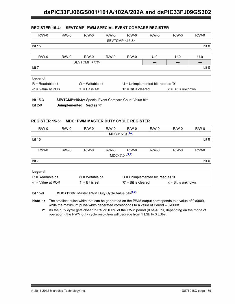
dsPIC33FJ06GS001/101A/102A/202A and dsPIC33FJ09GS302
REGISTER 15-4: SEVTCMP: PWM SPECIAL EVENT COMPARE REGISTER
R/W-0 R/W-0 R/W-0 R/W-0 R/W-0 R/W-0 R/W-0 R/W-0
SEVTCMP <15:8>
bit 15 bit 8
R/W-0 R/W-0 R/W-0 R/W-0 R/W-0 U-0 U-0 U-0
SEVTCMP <7:3> — — —
bit 7 bit 0
Legend:
R = Readable bit W = Writable bit U = Unimplemented bit, read as ‘0’
-n = Value at POR ‘1’ = Bit is set ‘0’ = Bit is cleared x = Bit is unknown
bit 15-3 SEVTCMP<15:3>: Special Event Compare Count Value bits
bit 2-0 Unimplemented: Read as ‘0’
REGISTER 15-5: MDC: PWM MASTER DUTY CYCLE REGISTER
R/W-0 R/W-0 R/W-0 R/W-0 R/W-0 R/W-0 R/W-0 R/W-0
MDC<15:8>(1,2)
bit 15 bit 8
R/W-0 R/W-0 R/W-0 R/W-0 R/W-0 R/W-0 R/W-0 R/W-0
MDC<7:0>(1,2)
bit 7 bit 0
Legend:
R = Readable bit W = Writable bit U = Unimplemented bit, read as ‘0’
-n = Value at POR ‘1’ = Bit is set ‘0’ = Bit is cleared x = Bit is unknown
bit 15-0 MDC<15:0>: Master PWM Duty Cycle Value bits(1,2)
Note 1: The smallest pulse width that can be generated on the PWM output corresponds to a value of 0x0009, while the maximum pulse width generated corresponds to a value of Period – 0x0008.
2: As the duty cycle gets closer to 0% or 100% of the PWM period (0 ns-40 ns, depending on the mode of operation), the PWM duty cycle resolution will degrade from 1 LSb to 3 LSbs.
2011-2012 Microchip Technology Inc. DS75018C-page 189

dsPIC33FJ06GS001/101A/102A/202A and dsPIC33FJ09GS302
REGISTER 15-6: PWMCONx: PWMx CONTROL REGISTER
HS/HC-0 HS/HC-0 HS/HC-0 R/W-0 R/W-0 R/W-0 R/W-0 R/W-0
FLTSTAT(1) CLSTAT(1) TRGSTAT FLTIEN CLIEN TRGIEN ITB(3) MDCS(3)
bit 15 bit 8
R/W-0 R/W-0 U-0 U-0 U-0 R/W-0 R/W-0 R/W-0
DTC<1:0> — — — CAM(2,3) XPRES(4) IUE
bit 7 bit 0
Legend: HC = Hardware Clearable bit HS = Hardware Settable bit
R = Readable bit W = Writable bit U = Unimplemented bit, read as ‘0’
-n = Value at POR ‘1’ = Bit is set ‘0’ = Bit is cleared x = Bit is unknown
bit 15 FLTSTAT: Fault Interrupt Status bit(1)
1 = Fault interrupt is pending0 = No Fault interrupt is pending; this bit is cleared by setting FLTIEN = 0
bit 14 CLSTAT: Current-Limit Interrupt Status bit(1)
1 = Current-limit interrupt is pending0 = No current-limit interrupt is pending; this bit is cleared by setting CLIEN = 0
bit 13 TRGSTAT: Trigger Interrupt Status bit
1 = Trigger interrupt is pending0 = No trigger interrupt is pending; this bit is cleared by setting TRGIEN = 0
bit 12 FLTIEN: Fault Interrupt Enable bit
1 = Fault interrupt is enabled0 = Fault interrupt is disabled and the FLTSTAT bit is cleared
bit 11 CLIEN: Current-Limit Interrupt Enable bit
1 = Current-limit interrupt is enabled0 = Current-limit interrupt is disabled and the CLSTAT bit is cleared
bit 10 TRGIEN: Trigger Interrupt Enable bit
1 = A trigger event generates an interrupt request0 = Trigger event interrupts are disabled and the TRGSTAT bit is cleared
bit 9 ITB: Independent Time Base Mode bit(3)
1 = PHASEx/SPHASEx register provides time base period for this PWM generator0 = PTPER register provides timing for this PWM generator
bit 8 MDCS: Master Duty Cycle Register Select bit(3)
1 = MDC register provides duty cycle information for this PWM generator0 = PDCx/SDCx register provides duty cycle information for this PWM generator
bit 7-6 DTC<1:0>: Dead-Time Control bits
11 = Reserved10 = Dead-time function is disabled01 = Negative dead time actively applied for all output modes00 = Positive dead time actively applied for all output modes
bit 5-3 Unimplemented: Read as ‘0’
Note 1: Software must clear the interrupt status here and the corresponding IFSx bit in the interrupt controller.
2: The Independent Time Base mode (ITB = 1) must be enabled to use Center-Aligned mode. If ITB = 0, the CAM bit is ignored.
3: These bits should be changed only when PTEN = 0. Changing the clock selection during operation will yield unpredictable results.
4: To operate in External Period Reset mode, configure the CLMOD (FCLCONx<8>) bit = 0 and ITB (PWMCONx<9>) bit = 1.
DS75018C-page 190 2011-2012 Microchip Technology Inc.

dsPIC33FJ06GS001/101A/102A/202A and dsPIC33FJ09GS302
bit 2 CAM: Center-Aligned Mode Enable bit(2,3)
1 = Center-Aligned mode is enabled0 = Center-Aligned mode is disabled
bit 1 XPRES: External PWM Reset Control bit(4)
1 = Current-limit source resets time base for this PWM generator if it is in Independent Time Base mode0 = External pins do not affect PWM time base
bit 0 IUE: Immediate Update Enable bit
1 = Updates to the active MDC/PDCx/SDCx registers are immediate0 = Updates to the active MDC/PDCx/SDCx registers are synchronized to the PWM time base
REGISTER 15-6: PWMCONx: PWMx CONTROL REGISTER (CONTINUED)
Note 1: Software must clear the interrupt status here and the corresponding IFSx bit in the interrupt controller.
2: The Independent Time Base mode (ITB = 1) must be enabled to use Center-Aligned mode. If ITB = 0, the CAM bit is ignored.
3: These bits should be changed only when PTEN = 0. Changing the clock selection during operation will yield unpredictable results.
4: To operate in External Period Reset mode, configure the CLMOD (FCLCONx<8>) bit = 0 and ITB (PWMCONx<9>) bit = 1.
2011-2012 Microchip Technology Inc. DS75018C-page 191

dsPIC33FJ06GS001/101A/102A/202A and dsPIC33FJ09GS302
REGISTER 15-7: PDCx: PWMx GENERATOR DUTY CYCLE REGISTER(1)
R/W-0 R/W-0 R/W-0 R/W-0 R/W-0 R/W-0 R/W-0 R/W-0
PDCx<15:8>(2)
bit 15 bit 8
R/W-0 R/W-0 R/W-0 R/W-0 R/W-0 R/W-0 R/W-0 R/W-0
PDCx<7:0>(2)
bit 7 bit 0
Legend:
R = Readable bit W = Writable bit U = Unimplemented bit, read as ‘0’
-n = Value at POR ‘1’ = Bit is set ‘0’ = Bit is cleared x = Bit is unknown
bit 15-0 PDCx<15:0>: PWMx Generator # Duty Cycle Value bits(2)
Note 1: In Independent PWM mode, the PDCx register controls the PWMxH duty cycle only. In Complementary, Redundant and Push-Pull PWM modes, the PDCx register controls the duty cycle of both the PWMxH and PWMxL. The smallest pulse width that can be generated on the PWM output corresponds to a value of 0x0009, while the maximum pulse width generated corresponds to a value of Period-0x0008.
2: As the duty cycle gets closer to 0% or 100% of the PWM period (0 ns-40 ns, depending on the mode of operation), the PWM duty cycle resolution will degrade from 1 LSB to 3 LSBs.
REGISTER 15-8: SDCx: PWMx SECONDARY DUTY CYCLE REGISTER(1)
R/W-0 R/W-0 R/W-0 R/W-0 R/W-0 R/W-0 R/W-0 R/W-0
SDCx<15:8>(2)
bit 15 bit 8
R/W-0 R/W-0 R/W-0 R/W-0 R/W-0 R/W-0 R/W-0 R/W-0
SDCx<7:0>(2)
bit 7 bit 0
Legend:
R = Readable bit W = Writable bit U = Unimplemented bit, read as ‘0’
-n = Value at POR ‘1’ = Bit is set ‘0’ = Bit is cleared x = Bit is unknown
bit 15-0 SDCx<15:0>: Secondary Duty Cycle for PWMxL Output Pin bits(2)
Note 1: The SDCx register is used in Independent PWM mode only. When used in Independent PWM mode, the SDCx register controls the PWMxL duty cycle. The smallest pulse width that can be generated on the PWM output corresponds to a value of 0x0009, while the maximum pulse width generated corresponds to a value of Period-0x0008.
2: As the duty cycle gets closer to 0% or 100% of the PWM period (0 ns-40 ns, depending on the mode of operation), the PWM duty cycle resolution will degrade from 1 LSB to 3 LSBs.
DS75018C-page 192 2011-2012 Microchip Technology Inc.

dsPIC33FJ06GS001/101A/102A/202A and dsPIC33FJ09GS302
REGISTER 15-9: PHASEx: PWMx PRIMARY PHASE SHIFT REGISTER
R/W-0 R/W-0 R/W-0 R/W-0 R/W-0 R/W-0 R/W-0 R/W-0
PHASEx<15:8>(1,2)
bit 15 bit 8
R/W-0 R/W-0 R/W-0 R/W-0 R/W-0 R/W-0 R/W-0 R/W-0
PHASEx<7:0>(1,2)
bit 7 bit 0
Legend:
R = Readable bit W = Writable bit U = Unimplemented bit, read as ‘0’
-n = Value at POR ‘1’ = Bit is set ‘0’ = Bit is cleared x = Bit is unknown
bit 15-0 PHASEx<15:0>: PWMx Phase Shift Value or Independent Time Base Period for PWM Generator bits(1,2)
Note 1: If the ITB (PWMCONx<9>) bit = 0, the following applies based on the mode of operation:• Complementary, Redundant and Push-Pull Output mode (PMOD<1:0> (IOCONx<11:10>) = 00, 01
or 10), PHASEx<15:0> = Phase shift value for PWMxH and PWMxL outputs.• True Independent Output mode PMOD<1:0> (IOCONx<11:10>) = 11),
PHASEx<15:0> = Phase shift value for PWMxL only.
2: If the ITB (PWMCONx<9>) bit = 1, the following applies based on the mode of operation: • Complementary, Redundant and Push-Pull Output mode (PMOD<1:0> (IOCONx<11:10>) = 00, 01
or 10), PHASEx<15:0> = Independent time base period value for PWMxH and PWMxL.• True Independent Output mode PMOD<1:0> (IOCONx<11:10>) = 11),
PHASEx<15:0> = Independent time base period value for PWMxL only.• The smallest pulse width that can be generated on the PWM output corresponds to a value of
0x0008, while the maximum pulse width generated corresponds to a value of Period-0x0008.
2011-2012 Microchip Technology Inc. DS75018C-page 193

dsPIC33FJ06GS001/101A/102A/202A and dsPIC33FJ09GS302
REGISTER 15-10: SPHASEx: PWMx SECONDARY PHASE SHIFT REGISTER
R/W-0 R/W-0 R/W-0 R/W-0 R/W-0 R/W-0 R/W-0 R/W-0
SPHASEx<15:8>(1,2)
bit 15 bit 8
R/W-0 R/W-0 R/W-0 R/W-0 R/W-0 R/W-0 R/W-0 R/W-0
SPHASEx<7:0>(1,2)
bit 7 bit 0
Legend:
R = Readable bit W = Writable bit U = Unimplemented bit, read as ‘0’
-n = Value at POR ‘1’ = Bit is set ‘0’ = Bit is cleared x = Bit is unknown
bit 15-0 SPHASEx<15:0>: Secondary Phase Offset for PWMxL Output Pin bits(1,2)
(used in Independent PWM mode only)
Note 1: If the ITB (PWMCONx<9>) bit = 0, the following applies based on the mode of operation:• Complementary, Redundant and Push-Pull Output mode (PMOD<1:0> (IOCONx<11:10>) = 00, 01
or 10), SPHASEx<15:0> = Not used.• True Independent Output mode PMOD<1:0> (IOCONx<11:10>) = 11),
PHASEx<15:0> = Phase shift value for PWMxL only.
2: If the ITB (PWMCONx<9>) bit = 1, the following applies based on the mode of operation: • Complementary, Redundant and Push-Pull Output mode (PMOD<1:0> (IOCONx<11:10>) = 00, 01
or 10), SPHASEx<15:0> = Not used.• True Independent Output mode PMOD<1:0> (IOCONx<11:10>) = 11),
PHASEx<15:0> = Independent time base period value for PWMxL only.
DS75018C-page 194 2011-2012 Microchip Technology Inc.

dsPIC33FJ06GS001/101A/102A/202A and dsPIC33FJ09GS302
.
REGISTER 15-11: DTRx: PWMx DEAD-TIME REGISTER
U-0 U-0 R/W-0 R/W-0 R/W-0 R/W-0 R/W-0 R/W-0
— — DTRx<13:8>
bit 15 bit 8
R/W-0 R/W-0 R/W-0 R/W-0 R/W-0 R/W-0 R/W-0 R/W-0
DTRx<7:0>
bit 7 bit 0
Legend:
R = Readable bit W = Writable bit U = Unimplemented bit, read as ‘0’
-n = Value at POR ‘1’ = Bit is set ‘0’ = Bit is cleared x = Bit is unknown
bit 15-14 Unimplemented: Read as ‘0’
bit 13-0 DTRx<13:0>: Unsigned 14-Bit Dead-Time Value for PWMx Dead-Time Unit bits
REGISTER 15-12: ALTDTRx: PWMx ALTERNATE DEAD-TIME REGISTER
U-0 U-0 R/W-0 R/W-0 R/W-0 R/W-0 R/W-0 R/W-0
— — ALTDTRx<13:8>
bit 15 bit 8
R/W-0 R/W-0 R/W-0 R/W-0 R/W-0 R/W-0 R/W-0 R/W-0
ALTDTR <7:0>
bit 7 bit 0
Legend:
R = Readable bit W = Writable bit U = Unimplemented bit, read as ‘0’
-n = Value at POR ‘1’ = Bit is set ‘0’ = Bit is cleared x = Bit is unknown
bit 15-14 Unimplemented: Read as ‘0’
bit 13-0 ALTDTRx<13:0>: Unsigned 14-Bit Dead-Time Value for PWMx Dead-Time Unit bits
2011-2012 Microchip Technology Inc. DS75018C-page 195

dsPIC33FJ06GS001/101A/102A/202A and dsPIC33FJ09GS302
REGISTER 15-13: TRGCONx: PWMx TRIGGER CONTROL REGISTER
R/W-0 R/W-0 R/W-0 R/W-0 U-0 U-0 U-0 U-0
TRGDIV<3:0> — — — —
bit 15 bit 8
R/W-0 U-0 R/W-0 R/W-0 R/W-0 R/W-0 R/W-0 R/W-0
DTM(1) — TRGSTRT<5:0>
bit 7 bit 0
Legend:
R = Readable bit W = Writable bit U = Unimplemented bit, read as ‘0’
-n = Value at POR ‘1’ = Bit is set ‘0’ = Bit is cleared x = Bit is unknown
bit 15-12 TRGDIV<3:0>: Trigger # Output Divider bits
1111 = Trigger output for every 16th trigger event1110 = Trigger output for every 15th trigger event1101 = Trigger output for every 14th trigger event1100 = Trigger output for every 13th trigger event1011 = Trigger output for every 12th trigger event1010 = Trigger output for every 11th trigger event1001 = Trigger output for every 10th trigger event1000 = Trigger output for every 9th trigger event0111 = Trigger output for every 8th trigger event0110 = Trigger output for every 7th trigger event0101 = Trigger output for every 6th trigger event0100 = Trigger output for every 5th trigger event0011 = Trigger output for every 4th trigger event0010 = Trigger output for every 3rd trigger event0001 = Trigger output for every 2nd trigger event0000 = Trigger output for every trigger event
bit 11-8 Unimplemented: Read as ‘0’
bit 7 DTM: Dual Trigger Mode bit(1)
1 = Secondary trigger event is combined with the primary trigger event to create the PWM trigger.0 = Secondary trigger event is not combined with the primary trigger event to create the PWM trigger;
two separate PWM triggers are generated
bit 6 Unimplemented: Read as ‘0’
bit 5-0 TRGSTRT<5:0>: Trigger Postscaler Start Enable Select bits
111111 = Wait 63 PWM cycles before generating the first trigger event after the module is enabled
•
•
•
000010 = Wait 2 PWM cycles before generating the first trigger event after the module is enabled000001 = Wait 1 PWM cycle before generating the first trigger event after the module is enabled000000 = Wait 0 PWM cycle before generating the first trigger event after the module is enabled
Note 1: The secondary generator cannot generate PWM trigger interrupts.
DS75018C-page 196 2011-2012 Microchip Technology Inc.

dsPIC33FJ06GS001/101A/102A/202A and dsPIC33FJ09GS302
REGISTER 15-14: IOCONx: PWMx I/O CONTROL REGISTER
R/W-0 R/W-0 R/W-0 R/W-0 R/W-0 R/W-0 R/W-0 R/W-0
PENH PENL POLH POLL PMOD<1:0>(1) OVRENH OVRENL
bit 15 bit 8
R/W-0 R/W-0 R/W-0 R/W-0 R/W-0 R/W-0 R/W-0 R/W-0
OVRDAT<1:0> FLTDAT<1:0>(2) CLDAT<1:0>(2) SWAP OSYNC
bit 7 bit 0
Legend:
R = Readable bit W = Writable bit U = Unimplemented bit, read as ‘0’
-n = Value at POR ‘1’ = Bit is set ‘0’ = Bit is cleared x = Bit is unknown
bit 15 PENH: PWMxH Output Pin Ownership bit
1 = PWM module controls PWMxH pin0 = GPIO module controls PWMxH pin
bit 14 PENL: PWMxL Output Pin Ownership bit
1 = PWM module controls PWMxL pin0 = GPIO module controls PWMxL pin
bit 13 POLH: PWMxH Output Pin Polarity bit
1 = PWMxH pin is active-low0 = PWMxH pin is active-high
bit 12 POLL: PWMxL Output Pin Polarity bit
1 = PWMxL pin is active-low0 = PWMxL pin is active-high
bit 11-10 PMOD<1:0>: PWMx I/O Pin Mode bits(1)
11 = PWM I/O pin pair is in the True Independent Output mode 10 = PWM I/O pin pair is in the Push-Pull Output mode01 = PWM I/O pin pair is in the Redundant Output mode00 = PWM I/O pin pair is in the Complementary Output mode
bit 9 OVRENH: Override Enable for PWMxH Pin bit
1 = OVRDAT<1> provides data for output on PWMxH pin0 = PWM generator provides data for PWMxH pin
bit 8 OVRENL: Override Enable for PWMxL Pin bit
1 = OVRDAT<0> provides data for output on PWMxL pin0 = PWM generator provides data for PWMxL pin
bit 7-6 OVRDAT<1:0>: Data for PWMxH and PWMxL Pins if Override is Enabled bits
If OVERENH = 1 then OVRDAT<1> provides data for PWMxH.If OVERENL = 1 then OVRDAT<0> provides data for PWMxL.
bit 5-4 FLTDAT<1:0>: State for PWMxH and PWMxL Pins if FLTMOD is Enabled bits(2)
IFLTMOD (FCLCONx<15>) = 0, Normal Fault mode:If Fault is active, then FLTDAT<1> provides the state for PWMxH.If Fault is active, then FLTDAT<0> provides the state for PWMxL.
IFLTMOD (FCLCONx<15>) = 1, Independent Fault mode:If current-limit is active, then FLTDAT<1> provides the state for PWMxH.If Fault is active, then FLTDAT<0> provides the state for PWMxL.
Note 1: These bits should be changed only when PTEN = 0. Changing the clock selection during operation will yield unpredictable results.
2: State represents the active/inactive state of the PWM module depending on the POLH and POLL bit settings.
2011-2012 Microchip Technology Inc. DS75018C-page 197

dsPIC33FJ06GS001/101A/102A/202A and dsPIC33FJ09GS302
bit 3-2 CLDAT<1:0>: State for PWMxH and PWMxL Pins if CLMODE is Enabled bits(2)
IFLTMOD (FCLCONx<15>) = 0, Normal Fault mode:If current-limit is active, then CLDAT<1> provides the state for PWMxH.If current-limit is active, then CLDAT<0> provides the state for PWMxL.
IFLTMOD (FCLCONx<15>) = 1, Independent Fault mode:CLDAT<1:0> is ignored.
bit 1 SWAP<1:0>: SWAP PWMxH and PWMxL pins
1 = PWMxH output signal is connected to PWMxL pin and PWMxL signal is connected to PWMxH pins0 = PWMxH and PWMxL pins are mapped to their respective pins
bit 0 OSYNC: Output Override Synchronization bit
1 = Output overrides via the OVRDAT<1:0> bits are synchronized to the PWM time base0 = Output overrides via the OVRDAT<1:0> bits occur on next CPU clock boundary
REGISTER 15-14: IOCONx: PWMx I/O CONTROL REGISTER (CONTINUED)
Note 1: These bits should be changed only when PTEN = 0. Changing the clock selection during operation will yield unpredictable results.
2: State represents the active/inactive state of the PWM module depending on the POLH and POLL bit settings.
DS75018C-page 198 2011-2012 Microchip Technology Inc.

dsPIC33FJ06GS001/101A/102A/202A and dsPIC33FJ09GS302
REGISTER 15-15: FCLCONx: PWMx FAULT CURRENT-LIMIT CONTROL REGISTER
R/W-0 R/W-0 R/W-0 R/W-0 R/W-0 R/W-0 R/W-0 R/W-0
IFLTMOD CLSRC<4:0>(2,3) CLPOL(1) CLMOD
bit 15 bit 8
R/W-0 R/W-0 R/W-0 R/W-0 R/W-0 R/W-0 R/W-0 R/W-0
FLTSRC<4:0>(2,3) FLTPOL(1) FLTMOD<1:0>
bit 7 bit 0
Legend:
R = Readable bit W = Writable bit U = Unimplemented bit, read as ‘0’
-n = Value at POR ‘1’ = Bit is set ‘0’ = Bit is cleared x = Bit is unknown
bit 15 IFLTMOD: Independent Fault Mode Enable bit
1 = Independent Fault mode: Current-limit input maps FLTDAT<1> to PWMxH output and Fault input maps FLTDAT<0> to PWMxL output. The CLDAT<1:0> bits are not used for override functions.0 = Normal Fault mode: Current-limit feature maps CLDAT<1:0> bits to the PWMxH and PWMxL
outputs. The PWM Fault feature maps FLTDAT<1:0> to the PWMxH and PWMxL outputs.
bit 14-10 CLSRC<4:0>: Current-Limit Control Signal Source Select for PWMx # Generator bits(2,3)
11111 = Reserved
•
•
•
01000 = Reserved
00111 = Fault 800110 = Fault 700101 = Fault 600100 = Fault 500011 = Fault 400010 = Fault 300001 = Fault 200000 = Fault 1
bit 9 CLPOL: Current-Limit Polarity for PWMx Generator # bit(1)
1 = The selected current-limit source is active-low0 = The selected current-limit source is active-high
bit 8 CLMOD: Current-Limit Mode Enable bit for PWMx Generator # bit1 = Current-limit function is enabled0 = Current-limit function is disabled
Note 1: These bits should be changed only when PTEN = 0. Changing the clock selection during operation will yield unpredictable results.
2: When Independent Fault mode is enabled (IFLTMOD<1:0> = 1), and Fault 1 is used for Current-Limit mode (CLSRC<4:0> = b0000), the Fault Control Source Select bits (FLTSRC<4:0>) should be set to an unused Fault source to prevent Fault 1 from disabling both the PWMxL and PWMxH outputs.
3: When Independent Fault mode is enabled (IFLTMOD<1:0> = 1) and Fault 1 is used for Fault mode (FLTSRC<4:0> = b0000), the Current-Limit Control Source Select bits (CLSRC<4:0>) should be set to an unused current-limit source to prevent the current-limit source from disabling both the PWMxH and PWMxL outputs.
2011-2012 Microchip Technology Inc. DS75018C-page 199

dsPIC33FJ06GS001/101A/102A/202A and dsPIC33FJ09GS302
bit 7-3 FLTSRC<4:0>: Fault Control Signal Source Select for PWM Generator # bits(2,3)
11111 = Reserved
•
•
•
01000 = Reserved
00111 = Fault 800110 = Fault 700101 = Fault 600100 = Fault 500011 = Fault 400010 = Fault 300001 = Fault 200000 = Fault 1
bit 2 FLTPOL: Fault Polarity for PWMx Generator # bit(1)
1 = The selected Fault source is active-low0 = The selected Fault source is active-high
bit 1-0 FLTMOD<1:0>: Fault Mode for PWMx Generator # bits
11 = Fault input is disabled10 = Reserved01 = The selected Fault source forces PWMxH, PWMxL pins to FLTDAT values (cycle)00 = The selected Fault source forces PWMxH, PWMxL pins to FLTDAT values (latched condition)
REGISTER 15-15: FCLCONx: PWMx FAULT CURRENT-LIMIT CONTROL REGISTER (CONTINUED)
Note 1: These bits should be changed only when PTEN = 0. Changing the clock selection during operation will yield unpredictable results.
2: When Independent Fault mode is enabled (IFLTMOD<1:0> = 1), and Fault 1 is used for Current-Limit mode (CLSRC<4:0> = b0000), the Fault Control Source Select bits (FLTSRC<4:0>) should be set to an unused Fault source to prevent Fault 1 from disabling both the PWMxL and PWMxH outputs.
3: When Independent Fault mode is enabled (IFLTMOD<1:0> = 1) and Fault 1 is used for Fault mode (FLTSRC<4:0> = b0000), the Current-Limit Control Source Select bits (CLSRC<4:0>) should be set to an unused current-limit source to prevent the current-limit source from disabling both the PWMxH and PWMxL outputs.
DS75018C-page 200 2011-2012 Microchip Technology Inc.

dsPIC33FJ06GS001/101A/102A/202A and dsPIC33FJ09GS302
REGISTER 15-16: TRIGx: PWMx PRIMARY TRIGGER COMPARE VALUE REGISTER
R/W-0 R/W-0 R/W-0 R/W-0 R/W-0 R/W-0 R/W-0 R/W-0
TRGCMP<15:8>
bit 15 bit 8
R/W-0 R/W-0 R/W-0 R/W-0 R/W-0 U-0 U-0 U-0
TRGCMP<7:3> — — —
bit 7 bit 0
Legend:
R = Readable bit W = Writable bit U = Unimplemented bit, read as ‘0’
-n = Value at POR ‘1’ = Bit is set ‘0’ = Bit is cleared x = Bit is unknown
bit 15-3 TRGCMP<15:3>: Trigger Control Value bits
When primary PWM functions in local time base, this register contains the compare values that can trigger the ADC module.
bit 2-0 Unimplemented: Read as ‘0’
REGISTER 15-17: STRIGx: PWMx SECONDARY TRIGGER COMPARE VALUE REGISTER
R/W-0 R/W-0 R/W-0 R/W-0 R/W-0 R/W-0 R/W-0 R/W-0
STRGCMP<15:8>
bit 15 bit 8
R/W-0 R/W-0 R/W-0 R/W-0 R/W-0 U-0 U-0 U-0
STRGCMP<7:3> — — —
bit 7 bit 0
Legend:
R = Readable bit W = Writable bit U = Unimplemented bit, read as ‘0’
-n = Value at POR ‘1’ = Bit is set ‘0’ = Bit is cleared x = Bit is unknown
bit 15-3 STRGCMP<15:3>: Secondary Trigger Control Value bits
When secondary PWM functions in local time base, this register contains the compare values that can trigger the ADC module.
bit 2-0 Unimplemented: Read as ‘0’
2011-2012 Microchip Technology Inc. DS75018C-page 201

dsPIC33FJ06GS001/101A/102A/202A and dsPIC33FJ09GS302
REGISTER 15-18: LEBCONx: PWMx LEADING-EDGE BLANKING CONTROL REGISTER
R/W-0 R/W-0 R/W-0 R/W-0 R/W-0 R/W-0 R/W-0 R/W-0
PHR PHF PLR PLF FLTLEBEN CLLEBEN LEB<6:5>
bit 15 bit 8
R/W-0 R/W-0 R/W-0 R/W-0 R/W-0 U-0 U-0 U-0
LEB<4:0> — — —
bit 7 bit 0
Legend:
R = Readable bit W = Writable bit U = Unimplemented bit, read as ‘0’
-n = Value at POR ‘1’ = Bit is set ‘0’ = Bit is cleared x = Bit is unknown
bit 15 PHR: PWMxH Rising Edge Trigger Enable bit
1 = Rising edge of PWMxH will trigger LEB counter0 = LEB ignores rising edge of PWMxH
bit 14 PHF: PWMxH Falling Edge Trigger Enable bit
1 = Falling edge of PWMxH will trigger LEB counter0 = LEB ignores falling edge of PWMxH
bit 13 PLR: PWMxL Rising Edge Trigger Enable bit
1 = Rising edge of PWMxL will trigger LEB counter0 = LEB ignores rising edge of PWMxL
bit 12 PLF: PWMxL Falling Edge Trigger Enable bit
1 = Falling edge of PWMxL will trigger LEB counter0 = LEB ignores falling edge of PWMxL
bit 11 FLTLEBEN: Fault Input LEB Enable bit
1 = Leading-edge blanking is applied to selected Fault input0 = Leading-edge blanking is not applied to selected Fault input
bit 10 CLLEBEN: Current-Limit LEB Enable bit
1 = Leading-edge blanking is applied to selected current-limit input0 = Leading-edge blanking is not applied to selected current-limit input
bit 9-3 LEB<6:0>: Leading-Edge Blanking for Current-Limit and Fault Inputs bits
The value is 8.32 nsec increments.
bit 2-0 Unimplemented: Read as ‘0’
DS75018C-page 202 2011-2012 Microchip Technology Inc.

dsPIC33FJ06GS001/101A/102A/202A and dsPIC33FJ09GS302
REGISTER 15-19: PWMCAPx: PRIMARY PWMx TIME BASE CAPTURE REGISTER
R-0 R-0 R-0 R-0 R-0 R-0 R-0 R-0
PWMCAP<15:8>(1,2)
bit 15 bit 8
R-0 R-0 R-0 R-0 R-0 U-0 U-0 U-0
PWMCAP<7:3>(1,2) — — —
bit 7 bit 0
Legend:
R = Readable bit W = Writable bit U = Unimplemented bit, read as ‘0’
-n = Value at POR ‘1’ = Bit is set ‘0’ = Bit is cleared x = Bit is unknown
bit 15-3 PWMCAP<15:3>: Captured PWM Time Base Value bits(1,2)
The value in this register represents the captured PWM time base value when a leading edge isdetected on the current-limit input.
bit 2-0 Unimplemented: Read as ‘0’
Note 1: The capture feature is only available on primary output (PWMxH).
2: This feature is active only after LEB processing on the current-limit input signal is complete.
REGISTER 15-20: CHOP: PWM CHOP CLOCK GENERATOR REGISTER
R/W-0 U-0 U-0 U-0 U-0 U-0 R/W-0 R/W-0
CHPCLKEN — — — — — CHOPCLK<6:5>
bit 15 bit 8
R/W-0 R/W-0 R/W-0 R/W-0 R/W-0 U-0 U-0 U-0
CHOPCLK<4:0> — — —
bit 7 bit 0
Legend:
R = Readable bit W = Writable bit U = Unimplemented bit, read as ‘0’
-n = Value at POR ‘1’ = Bit is set ‘0’ = Bit is cleared x = Bit is unknown
bit 15 CHPCLKEN: Enable Chop Clock Generator bit
1 = Chop clock generator is enabled0 = Chop clock generator is disabled
bit 14-10 Unimplemented: Read as ‘0’
bit 9-3 CHOPCLK<6:0>: Chop Clock Divider bits
The frequency of the chop clock signal is given by the following expression:Chop Frequency = 1/(16.64 * (CHOPCLK<6:0> + 1) * Primary Master PWM Input Clock/PCLKDIV<2:0>)
bit 2-0 Unimplemented: Read as ‘0’
2011-2012 Microchip Technology Inc. DS75018C-page 203

dsPIC33FJ06GS001/101A/102A/202A and dsPIC33FJ09GS302
REGISTER 15-21: AUXCONx: PWMx AUXILIARY CONTROL REGISTER
R/W-0 R/W-0 U-0 U-0 U-0 U-0 U-0 UW-0
HRPDIS HRDDIS — — — — — —
bit 15 bit 8
U-0 U-0 R/W-0 R/W-0 R/W-0 R/W-0 R/W-0 R/W-0
— — CHOPSEL<3:0> CHOPHEN CHOPLEN
bit 7 bit 0
Legend:
R = Readable bit W = Writable bit U = Unimplemented bit, read as ‘0’
-n = Value at POR ‘1’ = Bit is set ‘0’ = Bit is cleared x = Bit is unknown
bit 15 HRPDIS: High-Resolution PWMx Period Disable bit
1 = High-resolution PWMx period is enabled0 = High-resolution PWMx period is disabled
bit 14 HRDDIS: High-Resolution PWMx Duty Cycle Disable bit
1 = High-resolution PWMx duty cycle is enabled0 = High-resolution PWMx duty cycle is disabled
bit 13-6 Unimplemented: Read as ‘0’
bit 5-2 CHOPSEL<3:0>: PWMx Chop Clock Source Select bits
The selected signal will enable and disable (CHOP) the selected PWMx outputs.1001 = Reserved1000 = Reserved0111 = Reserved0110 = Reserved0101 = Reserved0100 = PWM4H is selected as CHOP clock source0011 = Reserved0010 = PWM2H is selected as CHOP clock source0001 = PWM1H is selected as CHOP clock source0000 = Chop clock generator is selected as CHOP clock source
bit 1 CHOPHEN: PWMxH Output Chopping Enable bit
1 = PWMxH chopping function is enabled0 = PWMxH chopping function is disabled
bit 0 CHOPLEN: PWMxL Output Chopping Enable bit
1 = PWMxL chopping function is enabled0 = PWMxL chopping function is disabled
DS75018C-page 204 2011-2012 Microchip Technology Inc.
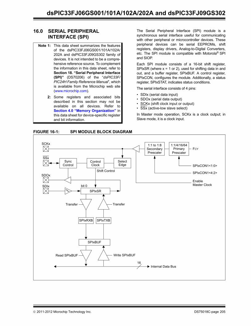
dsPIC33FJ06GS001/101A/102A/202A and dsPIC33FJ09GS302
16.0 SERIAL PERIPHERAL INTERFACE (SPI)
The Serial Peripheral Interface (SPI) module is asynchronous serial interface useful for communicatingwith other peripheral or microcontroller devices. Theseperipheral devices can be serial EEPROMs, shiftregisters, display drivers, Analog-to-Digital Converters,etc. The SPI module is compatible with Motorola® SPIand SIOP.
Each SPI module consists of a 16-bit shift register,SPIxSR (where x = 1 or 2), used for shifting data in andout, and a buffer register, SPIxBUF. A control register,SPIxCON, configures the module. Additionally, a statusregister, SPIxSTAT, indicates status conditions.
The serial interface consists of 4 pins:
• SDIx (serial data input)• SDOx (serial data output)• SCKx (shift clock input or output)• SSx (active-low slave select)
In Master mode operation, SCKx is a clock output; inSlave mode, it is a clock input.
FIGURE 16-1: SPI MODULE BLOCK DIAGRAM
Note 1: This data sheet summarizes the featuresof the dsPIC33FJ06GS001/101A/102A/202A and dsPIC33FJ09GS302 family ofdevices. It is not intended to be a compre-hensive reference source. To complementthe information in this data sheet, refer toSection 18. “Serial Peripheral Interface(SPI)” (DS70206) of the “dsPIC33F/PIC24H Family Reference Manual”, whichis available from the Microchip web site(www.microchip.com).
2: Some registers and associated bitsdescribed in this section may not beavailable on all devices. Refer toSection 4.0 “Memory Organization” inthis data sheet for device-specific registerand bit information.
Internal Data Bus
SDIx
SDOx
SSx
SCKx
SPIxSR
bit 0
Shift Control
EdgeSelect
FCYPrimary1:1/4/16/64
Enable
Prescaler
Sync
SPIxBUF
Control
TransferTransfer
Write SPIxBUFRead SPIxBUF
16
SPIxCON1<1:0>
SPIxCON1<4:2>
Master Clock
ClockControl
SecondaryPrescaler
1:1 to 1:8
SPIxRXB SPIxTXB
2011-2012 Microchip Technology Inc. DS75018C-page 205

dsPIC33FJ06GS001/101A/102A/202A and dsPIC33FJ09GS302
16.1 SPI Helpful Tips
1. In Frame mode, if there is a possibility that themaster may not be initialized before the slave:
a) If FRMPOL (SPIxCON2<13>) = 1, use apull-down resistor on SSx.
b) If FRMPOL = 0, use a pull-up resistor onSSx.
2. In Non-Framed 3-Wire mode, (i.e., not usingSSx from a master):
a) If CKP (SPIxCON1<6>) = 1, always place apull-up resistor on SSx.
b) If CKP = 0, always place a pull-downresistor on SSx.
3. FRMEN (SPIxCON2<15>) = 1 and SSEN(SPIxCON1<7>) = 1 are exclusive and invalid.In Frame mode, SCKx is continuous and theFrame Sync pulse is active on the SSx pin,which indicates the start of a data frame.
4. In Master mode only, set the SMP bit(SPIxCON1<9>) to a ‘1’ for the fastest SPI datarate possible. The SMP bit can only be set at thesame time or after the MSTEN bit(SPIxCON1<5>) is set.
To avoid invalid slave read data to the master, theuser’s master software must ensure enough time forslave software to fill its write buffer before the userapplication initiates a master write/read cycle. It isalways advisable to preload the SPIxBUF Transmitregister in advance of the next master transactioncycle. SPIxBUF is transferred to the SPI Shift registerand is empty once the data transmission begins.
16.2 SPI Resources
Many useful resources related to SPI are provided onthe Microchip web site (www.microchip.com).
16.2.1 KEY RESOURCES
• Section 18. “Serial Peripheral Interface (SPI)” (DS70206)
• Code Samples
• Application Notes
• Software Libraries
• Webinars
• All related “dsPIC33F/PIC24H Family Reference Manual” Sections
• Development Tools
Note: This insures that the first frametransmission after initialization is notshifted or corrupted.
Note: This will insure that during power-up andinitialization the master/slave will not loseSync due to an errant SCK transition thatwould cause the slave to accumulate datashift errors for both transmit and receiveappearing as corrupted data.
Note: Not all third-party devices support Framemode timing. Refer to the SPI electricalcharacteristics for details.
DS75018C-page 206 2011-2012 Microchip Technology Inc.

dsPIC33FJ06GS001/101A/102A/202A and dsPIC33FJ09GS302
16.3 SPI Control Registers
REGISTER 16-1: SPIxSTAT: SPIx STATUS AND CONTROL REGISTER
R/W-0 U-0 R/W-0 U-0 U-0 U-0 U-0 U-0
SPIEN — SPISIDL — — — — —
bit 15 bit 8
U-0 R/C-0 U-0 U-0 U-0 U-0 R-0 R-0
— SPIROV — — — — SPITBF SPIRBF
bit 7 bit 0
Legend: C = Clearable bit
R = Readable bit W = Writable bit U = Unimplemented bit, read as ‘0’
-n = Value at POR ‘1’ = Bit is set ‘0’ = Bit is cleared x = Bit is unknown
bit 15 SPIEN: SPIx Enable bit
1 = Enables module and configures SCKx, SDOx, SDIx and SSx as serial port pins0 = Disables module
bit 14 Unimplemented: Read as ‘0’
bit 13 SPISIDL: Stop in Idle Mode bit
1 = Discontinues module operation when device enters Idle mode0 = Continues module operation in Idle mode
bit 12-7 Unimplemented: Read as ‘0’
bit 6 SPIROV: Receive Overflow Flag bit1 = A new byte/word is completely received and discarded; the user software has not read the previous
data in the SPIxBUF register0 = No overflow has occurred
bit 5-2 Unimplemented: Read as ‘0’
bit 1 SPITBF: SPIx Transmit Buffer Full Status bit
1 = Transmit not yet started, SPIxTXB is full0 = Transmit started, SPIxTXB is emptyAutomatically set in hardware when the CPU writes to the SPIxBUF location, loading SPIxTXB.Automatically cleared in hardware when the SPIx module transfers data from SPIxTXB to SPIxSR.
bit 0 SPIRBF: SPIx Receive Buffer Full Status bit
1 = Receive is complete, SPIxRXB is full0 = Receive is not complete, SPIxRXB is emptyAutomatically set in hardware when SPIx transfers data from SPIxSR to SPIxRXB.Automatically cleared in hardware when core reads the SPIxBUF location, reading SPIxRXB.
2011-2012 Microchip Technology Inc. DS75018C-page 207

dsPIC33FJ06GS001/101A/102A/202A and dsPIC33FJ09GS302
REGISTER 16-2: SPIXCON1: SPIx CONTROL REGISTER 1
U-0 U-0 U-0 R/W-0 R/W-0 R/W-0 R/W-0 R/W-0
— — — DISSCK DISSDO MODE16 SMP CKE(1)
bit 15 bit 8
R/W-0 R/W-0 R/W-0 R/W-0 R/W-0 R/W-0 R/W-0 R/W-0
SSEN(3) CKP MSTEN SPRE<2:0>(2) PPRE<1:0>(2)
bit 7 bit 0
Legend:
R = Readable bit W = Writable bit U = Unimplemented bit, read as ‘0’
-n = Value at POR ‘1’ = Bit is set ‘0’ = Bit is cleared x = Bit is unknown
bit 15-13 Unimplemented: Read as ‘0’
bit 12 DISSCK: Disable SCKx Pin bit (SPI Master modes only)
1 = Internal SPI clock is disabled; pin functions as I/O0 = Internal SPI clock is enabled
bit 11 DISSDO: Disable SDOx Pin bit
1 = SDOx pin is not used by module; pin functions as I/O0 = SDOx pin is controlled by the module
bit 10 MODE16: Word/Byte Communication Select bit
1 = Communication is word-wide (16 bits)0 = Communication is byte-wide (8 bits)
bit 9 SMP: SPIx Data Input Sample Phase bit
Master mode:1 = Input data is sampled at end of data output time0 = Input data is sampled at middle of data output time
Slave mode:SMP must be cleared when SPIx is used in Slave mode.
bit 8 CKE: SPIx Clock Edge Select bit(1)
1 = Serial output data changes on transition from active clock state to Idle clock state (see bit 6)0 = Serial output data changes on transition from Idle clock state to active clock state (see bit 6)
bit 7 SSEN: Slave Select Enable bit (Slave mode)(3)
1 = SSx pin is used for Slave mode0 = SSx pin is not used by module; pin is controlled by port function
bit 6 CKP: Clock Polarity Select bit
1 = Idle state for clock is a high level; active state is a low level0 = Idle state for clock is a low level; active state is a high level
bit 5 MSTEN: Master Mode Enable bit
1 = Master mode0 = Slave mode
Note 1: This bit is not used in Framed SPI modes. Program this bit to ‘0’ for the Framed SPI modes (FRMEN = 1).
2: Do not set both Primary and Secondary prescalers to a value of 1:1.
3: This bit must be cleared when FRMEN = 1.
DS75018C-page 208 2011-2012 Microchip Technology Inc.

dsPIC33FJ06GS001/101A/102A/202A and dsPIC33FJ09GS302
bit 4-2 SPRE<2:0>: Secondary Prescale bits (Master mode)(2)
111 = Secondary prescale 1:1110 = Secondary prescale 2:1
•
•
•
000 = Secondary prescale 8:1
bit 1-0 PPRE<1:0>: Primary Prescale bits (Master mode)(2)
11 = Primary prescale 1:110 = Primary prescale 4:101 = Primary prescale 16:100 = Primary prescale 64:1
REGISTER 16-2: SPIXCON1: SPIx CONTROL REGISTER 1 (CONTINUED)
Note 1: This bit is not used in Framed SPI modes. Program this bit to ‘0’ for the Framed SPI modes (FRMEN = 1).
2: Do not set both Primary and Secondary prescalers to a value of 1:1.
3: This bit must be cleared when FRMEN = 1.
2011-2012 Microchip Technology Inc. DS75018C-page 209

dsPIC33FJ06GS001/101A/102A/202A and dsPIC33FJ09GS302
REGISTER 16-3: SPIxCON2: SPIx CONTROL REGISTER 2
R/W-0 R/W-0 R/W-0 U-0 U-0 U-0 U-0 U-0
FRMEN SPIFSD FRMPOL — — — — —
bit 15 bit 8
U-0 U-0 U-0 U-0 U-0 U-0 R/W-0 U-0
— — — — — — FRMDLY —
bit 7 bit 0
Legend:
R = Readable bit W = Writable bit U = Unimplemented bit, read as ‘0’
-n = Value at POR ‘1’ = Bit is set ‘0’ = Bit is cleared x = Bit is unknown
bit 15 FRMEN: Framed SPIx Support bit
1 = Framed SPIx support enabled (SSx pin used as Frame Sync pulse input/output)0 = Framed SPIx support disabled
bit 14 SPIFSD: Frame Sync Pulse Direction Control bit
1 = Frame Sync pulse input (slave)0 = Frame Sync pulse output (master)
bit 13 FRMPOL: Frame Sync Pulse Polarity bit
1 = Frame Sync pulse is active-high0 = Frame Sync pulse is active-low
bit 12-2 Unimplemented: Read as ‘0’
bit 1 FRMDLY: Frame Sync Pulse Edge Select bit
1 = Frame Sync pulse coincides with first bit clock0 = Frame Sync pulse precedes first bit clock
bit 0 Unimplemented: This bit must not be set to ‘1’ by the user application
DS75018C-page 210 2011-2012 Microchip Technology Inc.

dsPIC33FJ06GS001/101A/102A/202A and dsPIC33FJ09GS302
17.0 INTER-INTEGRATED CIRCUIT™ (I2C™)
The Inter-Integrated Circuit™ (I2C™) module providescomplete hardware support for both Slave andMulti-Master modes of the I2C serial communicationstandard with a 16-bit interface.
The I2C module has a 2-pin interface:
• The SCL1 pin is the clock• The SDA1 pin is data
The I2C module offers the following key features:
• I2C interface supporting both Master and Slave modes of operation
• I2C Slave mode supports 7-bit and 10-bit addressing
• I2C Master mode supports 7-bit and 10-bit addressing
• I2C port allows bidirectional transfers between master and slaves
• Serial clock synchronization for I2C port can be used as a handshake mechanism to suspend and resume serial transfer (SCLREL control)
• I2C supports multi-master operation, detects bus collision and arbitrates accordingly
17.1 Operating Modes
The hardware fully implements all the master and slavefunctions of the I2C Standard and Fast modespecifications, as well as 7-bit and 10-bit addressing.
The I2C module can operate either as a slave or amaster on an I2C bus.
The following types of I2C operation are supported:
• I2C slave operation with 7-bit addressing
• I2C slave operation with 10-bit addressing
• I2C master operation with 7-bit or 10-bit addressing
For details about the communication sequence in eachof these modes, please see the Microchip web site(www.microchip.com) for the latest “dsPIC33F/PIC24HFamily Reference Manual” sections.
Note 1: This data sheet summarizes the featuresof the dsPIC33FJ06GS001/101A/102A/202A and dsPIC33FJ09GS302 families ofdevices. It is not intended to be a compre-hensive reference source. To complementthe information in this data sheet, refer toSection 19. “Inter-Integrated Circuit(I2C™)” (DS70195) in the “dsPIC33F/PIC24H Family Reference Manual”, whichis available on the Microchip web site(www.microchip.com).
2: Some registers and associated bitsdescribed in this section may not beavailable on all devices. Refer toSection 4.0 “Memory Organization” inthis data sheet for device-specific registerand bit information.
2011-2012 Microchip Technology Inc. DS75018C-page 211
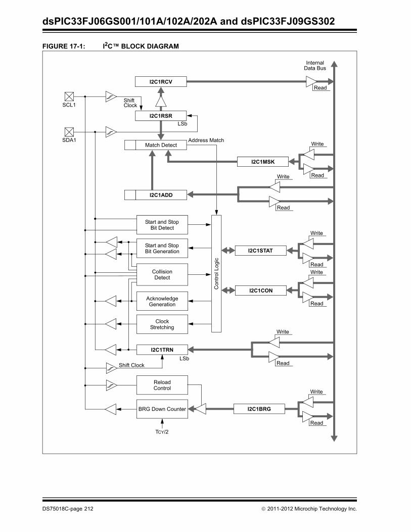
dsPIC33FJ06GS001/101A/102A/202A and dsPIC33FJ09GS302
FIGURE 17-1: I2C™ BLOCK DIAGRAM
InternalData Bus
SCL1
SDA1
Shift
Match Detect
I2C1ADD
Start and StopBit Detect
Clock
Address Match
ClockStretching
I2C1TRN
LSbShift Clock
BRG Down Counter
ReloadControl
TCY/2
Start and StopBit Generation
AcknowledgeGeneration
CollisionDetect
I2C1CON
I2C1STAT
Con
trol
Lo
gic
Read
LSb
Write
Read
I2C1BRG
I2C1RSR
Write
Read
Write
Read
Write
Read
Write
Read
Write
Read
I2C1MSK
I2C1RCV
DS75018C-page 212 2011-2012 Microchip Technology Inc.

dsPIC33FJ06GS001/101A/102A/202A and dsPIC33FJ09GS302
17.2 I2C Registers
I2C1CON and I2C1STAT are control and statusregisters, respectively. The I2C1CON register isreadable and writable. The lower six bits of I2C1STATare read-only. The remaining bits of the I2CSTAT areread/write:
• I2C1RSR is the shift register used for shifting data internal to the module and the user application has no access to it
• I2C1RCV is the receive buffer and the register to which data bytes are written, or from which data bytes are read
• I2C1TRN is the transmit register to which bytes are written during a transmit operation
• The I2C1ADD register holds the slave address
• A status bit, ADD10, indicates 10-Bit Address mode
• The I2C1BRG acts as the Baud Rate Generator (BRG) reload value
In receive operations, I2C1RSR and I2C1RCVtogether form a double-buffered receiver. WhenI2C1RSR receives a complete byte, it is transferred toI2C1RCV, and an interrupt pulse is generated.
REGISTER 17-1: I2C1CON: I2C1 CONTROL REGISTER
R/W-0 U-0 R/W-0 R/W-1, HC R/W-0 R/W-0 R/W-0 R/W-0
I2CEN — I2CSIDL SCLREL IPMIEN A10M DISSLW SMEN
bit 15 bit 8
R/W-0 R/W-0 R/W-0 R/W-0, HC R/W-0, HC R/W-0, HC R/W-0, HC R/W-0, HC
GCEN STREN ACKDT ACKEN RCEN PEN RSEN SEN
bit 7 bit 0
Legend: HC = Hardware Clearable bit
R = Readable bit W = Writable bit U = Unimplemented bit, read as ‘0’
-n = Value at POR ‘1’ = Bit is set ‘0’ = Bit is cleared x = Bit is unknown
bit 15 I2CEN: I2C1 Enable bit
1 = Enables the I2C1 module and configures the SDA1 and SCL1 pins as serial port pins0 = Disables the I2C1 module; all I2C pins are controlled by port functions
bit 14 Unimplemented: Read as ‘0’
bit 13 I2CSIDL: Stop in Idle Mode bit
1 = Discontinues module operation when device enters an Idle mode0 = Continues module operation in Idle mode
bit 12 SCLREL: SCL1 Release Control bit (when operating as I2C slave)
1 = Releases SCL1 clock0 = Holds SCL1 clock low (clock stretch)
If STREN = 1:Bit is R/W (i.e., software can write ‘0’ to initiate stretch and write ‘1’ to release clock). Hardware is clearat beginning of slave transmission. Hardware is clear at end of slave reception.
If STREN = 0:Bit is R/S (i.e., software can only write ‘1’ to release clock). Hardware is clear at beginning of slavetransmission.
bit 11 IPMIEN: Intelligent Peripheral Management Interface (IPMI) Enable bit
1 = IPMI mode is enabled; all addresses Acknowledged0 = IPMI mode is disabled
bit 10 A10M: 10-Bit Slave Address bit
1 = I2C1ADD is a 10-bit slave address0 = I2C1ADD is a 7-bit slave address
bit 9 DISSLW: Disable Slew Rate Control bit
1 = Slew rate control is disabled0 = Slew rate control is enabled
2011-2012 Microchip Technology Inc. DS75018C-page 213

dsPIC33FJ06GS001/101A/102A/202A and dsPIC33FJ09GS302
bit 8 SMEN: SMBus Input Levels bit
1 = Enables I/O pin thresholds compliant with SMBus specification0 = Disables SMBus input thresholds
bit 7 GCEN: General Call Enable bit (when operating as I2C slave)
1 = Enables interrupt when a general call address is received in the I2C1RSR(module is enabled for reception)
0 = General call address is disabled
bit 6 STREN: SCL1 Clock Stretch Enable bit (when operating as I2C slave)
Used in conjunction with SCLREL bit.1 = Enables software or receives clock stretching0 = Disables software or receives clock stretching
bit 5 ACKDT: Acknowledge Data bit (when operating as I2C master, applicable during master receive)
Value that is transmitted when the software initiates an Acknowledge sequence.1 = Sends NACK during Acknowledge0 = Sends ACK during Acknowledge
bit 4 ACKEN: Acknowledge Sequence Enable bit (when operating as I2C master, applicable during master receive)
1 = Initiates Acknowledge sequence on SDA1 and SCL1 pins and transmits ACKDT data bit.Hardware is clear at end of master Acknowledge sequence.
0 = Acknowledge sequence is not in progress
bit 3 RCEN: Receive Enable bit (when operating as I2C master)
1 = Enables Receive mode for I2C. Hardware is clear at end of eighth bit of master receive data byte.0 = Receive sequence is not in progress
bit 2 PEN: Stop Condition Enable bit (when operating as I2C master)
1 = Initiates Stop condition on SDA1 and SCL1 pins. Hardware is clear at end of master Stop sequence.0 = Stop condition is not in progress
bit 1 RSEN: Repeated Start Condition Enable bit (when operating as I2C master)
1 = Initiates Repeated Start condition on SDA1 and SCL1 pins. Hardware is clear at end of masterRepeated Start sequence.
0 = Repeated Start condition is not in progress
bit 0 SEN: Start Condition Enable bit (when operating as I2C master)
1 = Initiates Start condition on SDA1 and SCL1 pins. Hardware is clear at end of master Startsequence.
0 = Start condition is not in progress
REGISTER 17-1: I2C1CON: I2C1 CONTROL REGISTER (CONTINUED)
DS75018C-page 214 2011-2012 Microchip Technology Inc.

dsPIC33FJ06GS001/101A/102A/202A and dsPIC33FJ09GS302
REGISTER 17-2: I2C1STAT: I2C1 STATUS REGISTER
R-0, HSC R-0, HSC U-0 U-0 U-0 R/C-0, HSC R-0, HSC R-0, HSC
ACKSTAT TRSTAT — — — BCL GCSTAT ADD10
bit 15 bit 8
R/C-0, HS R/C-0, HS R-0, HSC R/C-0, HSC R/C-0, HSC R-0, HSC R-0, HSC R-0, HSC
IWCOL I2COV D_A P S R_W RBF TBF
bit 7 bit 0
Legend: HS = Hardware Settable bit’ HSC = Hardware Settable/Clearable bit
R = Readable bit W = Writable bit U = Unimplemented bit, read as ‘0’ C = Clearable bit
-n = Value at POR ‘1’ = Bit is set ‘0’ = Bit is cleared x = Bit is unknown
bit 15 ACKSTAT: Acknowledge Status bit (when operating as I2C master, applicable to master transmit operation)
1 = NACK is received from slave0 = ACK is received from slaveHardware is set or clear at end of slave Acknowledge.
bit 14 TRSTAT: Transmit Status bit (when operating as I2C master, applicable to master transmit operation)
1 = Master transmit is in progress (8 bits + ACK)0 = Master transmit is not in progressHardware is set at beginning of master transmission. Hardware is clear at end of slave Acknowledge.
bit 13-11 Unimplemented: Read as ‘0’
bit 10 BCL: Master Bus Collision Detect bit
1 = A bus collision has been detected during a master operation0 = No collisionHardware is set at detection of bus collision.
bit 9 GCSTAT: General Call Status bit
1 = General call address was received0 = General call address was not receivedHardware is set when address matches general call address. Hardware is clear at Stop detection.
bit 8 ADD10: 10-Bit Address Status bit
1 = 10-bit address was matched0 = 10-bit address was not matchedHardware is set at match of 2nd byte of matched 10-bit address. Hardware is clear at Stop detection.
bit 7 IWCOL: Write Collision Detect bit
1 = An attempt to write to the I2C1TRN register failed because the I2C module is busy 0 = No collisionHardware is set at occurrence of write to I2C1TRN while busy (cleared by software).
bit 6 I2COV: Receive Overflow Flag bit
1 = A byte was received while the I2C1RCV register is still holding the previous byte0 = No overflowHardware is set at attempt to transfer I2C1RSR to I2C1RCV (cleared by software).
bit 5 D_A: Data/Address bit (when operating as I2C slave)
1 = Indicates that the last byte received was data0 = Indicates that the last byte received was the device addressHardware is clear at device address match. Hardware is set by reception of slave byte.
bit 4 P: Stop bit
1 = Indicates that a Stop bit has been detected last0 = Stop bit was not detected lastHardware is set or clear when Start, Repeated Start or Stop is detected.
2011-2012 Microchip Technology Inc. DS75018C-page 215

dsPIC33FJ06GS001/101A/102A/202A and dsPIC33FJ09GS302
bit 3 S: Start bit
1 = Indicates that a Start (or Repeated Start) bit has been detected last0 = Start bit was not detected lastHardware is set or clear when Start, Repeated Start or Stop is detected.
bit 2 R_W: Read/Write Information bit (when operating as I2C slave)
1 = Read – indicates data transfer is output from slave0 = Write – indicates data transfer is input to slaveHardware is set or clear after reception of I2C device address byte.
bit 1 RBF: Receive Buffer Full Status bit
1 = Receive is complete, I2C1RCV is full0 = Receive is not complete, I2C1RCV is emptyHardware is set when I2C1RCV is written with received byte. Hardware is clear when software readsI2C1RCV.
bit 0 TBF: Transmit Buffer Full Status bit
1 = Transmit is in progress, I2C1TRN is full0 = Transmit is complete, I2C1TRN is emptyHardware is set when software writes I2C1TRN. Hardware is clear at completion of data transmission.
REGISTER 17-2: I2C1STAT: I2C1 STATUS REGISTER (CONTINUED)
DS75018C-page 216 2011-2012 Microchip Technology Inc.

dsPIC33FJ06GS001/101A/102A/202A and dsPIC33FJ09GS302
REGISTER 17-3: I2C1MSK: I2C1 SLAVE MODE ADDRESS MASK REGISTER
U-0 U-0 U-0 U-0 U-0 U-0 R/W-0 R/W-0
— — — — — — AMSK<9:8>
bit 15 bit 8
R/W-0 R/W-0 R/W-0 R/W-0 R/W-0 R/W-0 R/W-0 R/W-0
AMSK<7:0>
bit 7 bit 0
Legend:
R = Readable bit W = Writable bit U = Unimplemented bit, read as ‘0’
-n = Value at POR ‘1’ = Bit is set ‘0’ = Bit is cleared x = Bit is unknown
bit 15-10 Unimplemented: Read as ‘0’
bit 9-0 AMSK<9:0>: Mask for Address bit x Select bits
1 = Enables masking for bit x of incoming message address; bit match not required in this position0 = Disables masking for bit x; bit match required in this position
2011-2012 Microchip Technology Inc. DS75018C-page 217

dsPIC33FJ06GS001/101A/102A/202A and dsPIC33FJ09GS302
NOTES:
DS75018C-page 218 2011-2012 Microchip Technology Inc.

dsPIC33FJ06GS001/101A/102A/202A and dsPIC33FJ09GS302
18.0 UNIVERSAL ASYNCHRONOUS RECEIVER TRANSMITTER (UART)
The Universal Asynchronous Receiver Transmitter(UART) module is a serial I/O module. The UART is afull-duplex, asynchronous system that can communicatewith peripheral devices, such as personal computers,LIN/J2602, RS-232 and RS-485 interfaces. The modulealso supports a hardware flow control option with theU1CTS and U1RTS pins, and also includes an IrDA®
encoder and decoder.
The primary features of the UART module are:
• Full-duplex, 8-bit or 9-bit data transmission through the U1TX and U1RX pins
• Even, Odd or No Parity options (for 8-bit data)
• One or two Stop bits
• Hardware flow control option with U1CTS and U1RTS pins
• Fully integrated Baud Rate Generator (BRG) with 16-bit prescaler
• Baud rates ranging from 10 Mbps to 38 bps at40 MIPS
• 4-deep First-In First-Out (FIFO) transmit databuffer
• 4-deep FIFO receive data buffer
• Parity, framing and buffer overrun error detection
• Support for 9-bit mode with address detect(9th bit = 1)
• Transmit and Receive interrupts
• Separate interrupt for all UART error conditions
• Loopback mode for diagnostic support
• Support for Sync and Break characters
• Support for automatic baud rate detection
• IrDA encoder and decoder logic
• 16x baud clock output for IrDA® support
A simplified block diagram of the UART module isshown in Figure 18-1. The UART module consists ofthese key hardware elements:
• BRG
• Asynchronous transmitter
• Asynchronous receiver
FIGURE 18-1: UART SIMPLIFIED BLOCK DIAGRAM
Note 1: This data sheet summarizes the featuresof the dsPIC33FJ06GS001/101A/102A/202A and dsPIC33FJ09GS302 family ofdevices. It is not intended to be acomprehensive reference source. Tocomplement the information in this datasheet, refer to Section 17. “UART”(DS70188) in the “dsPIC33F/PIC24HFamily Reference Manual”, which isavailable on the Microchip web site(www.microchip.com).
2: Some registers and associated bitsdescribed in this section may not beavailable on all devices. Refer toSection 4.0 “Memory Organization” inthis data sheet for device-specific registerand bit information.
Note: The dsPIC33FJ06GS001 device does nothave a UART module.
U1RX
Hardware Flow Control
UART Receiver
UART Transmitter U1TX
Baud Rate Generator
U1RTS/BCLK
IrDA®
U1CTS
2011-2012 Microchip Technology Inc. DS75018C-page 219

dsPIC33FJ06GS001/101A/102A/202A and dsPIC33FJ09GS302
18.1 UART Helpful Tips
1. In multinode, direct-connect UART networks,UART receive inputs react to the complemen-tary logic level defined by the URXINV bit(U1MODE<4>), which defines the Idle state, thedefault of which is logic high, (i.e., URXINV = 0).Because remote devices do not initialize at thesame time, it is likely that one of the devices,because the RX line is floating, will trigger aStart bit detection and will cause the first bytereceived after the device has been initialized tobe invalid. To avoid this situation, the usershould use a pull-up or pull-down resistor on theRX pin, depending on the value of the URXINVbit.
a) If URXINV = 0, use a pull-up resistor on theRX pin.
b) If URXINV = 1, use a pull-down resistor onthe RX pin.
2. The first character received on a wake-up fromSleep mode, caused by activity on the UxRX pinof the UART module, will be invalid. In Sleepmode, peripheral clocks are disabled. By the timethe oscillator system has restarted and stabilizedfrom Sleep mode, the baud rate bit samplingclock, relative to the incoming UxRX bit timing, isno longer synchronized. This results in the firstcharacter being invalid; this is to be expected.
18.2 UART Resources
Many useful resources related to UART are providedon the Microchip web site (www.microchip.com).
18.2.1 KEY RESOURCES
• Section 17. “UART” (DS70188) in the “dsPIC33F/PIC24H Family Reference Manual”
• Code Samples
• Application Notes
• Software Libraries
• Webinars
• All related “dsPIC33F/PIC24H Family Reference Manual” Sections
• Development Tools
DS75018C-page 220 2011-2012 Microchip Technology Inc.

dsPIC33FJ06GS001/101A/102A/202A and dsPIC33FJ09GS302
18.3 UART Registers
REGISTER 18-1: U1MODE: UART1 MODE REGISTER
R/W-0 U-0 R/W-0 R/W-0 R/W-0 U-0 R/W-0 R/W-0
UARTEN(1,3) — USIDL(3) IREN(2,3) RTSMD(3) — UEN<1:0>(3)
bit 15 bit 8
R/W-0, HC R/W-0 R/W-0, HC R/W-0 R/W-0 R/W-0 R/W-0 R/W-0
WAKE(3) LPBACK(3) ABAUD(3) URXINV(3) BRGH(3) PDSEL<1:0>(3) STSEL(3)
bit 7 bit 0
Legend: HC = Hardware Clearable bit
R = Readable bit W = Writable bit U = Unimplemented bit, read as ‘0’
-n = Value at POR ‘1’ = Bit is set ‘0’ = Bit is cleared x = Bit is unknown
bit 15 UARTEN: UART1 Enable bit(1,3)
1 = UART1 is enabled; all UART1 pins are controlled by UART1, as defined by UEN<1:0>0 = UART1 is disabled; all UART1 pins are controlled by port latches; UART1 power consumption
is minimal
bit 14 Unimplemented: Read as ‘0’
bit 13 USIDL: Stop in Idle Mode bit(3)
1 = Discontinues module operation when device enters Idle mode0 = Continues module operation in Idle mode
bit 12 IREN: IrDA® Encoder and Decoder Enable bit(2,3)
1 = IrDA® encoder and decoder are enabled0 = IrDA® encoder and decoder are disabled
bit 11 RTSMD: Mode Selection for U1RTS Pin bit(3)
1 = U1RTS pin is in Simplex mode0 = U1RTS pin is in Flow Control mode
bit 10 Unimplemented: Read as ‘0’
bit 9-8 UEN<1:0>: UART1 Pin Enable bits(3)
11 = U1TX, U1RX and BCLK pins are enabled and used; U1CTS pin is controlled by port latches10 = U1TX, U1RX, U1CTS and U1RTS pins are enabled and used01 = U1TX, U1RX and U1RTS pins are enabled and used; U1CTS pin is controlled by port latches00 = U1TX and U1RX pins are enabled and used; U1CTS and U1RTS/BCLK pins are controlled by
port latches
bit 7 WAKE: Wake-up on Start bit Detect During Sleep Mode Enable bit(3)
1 = UART1 will continue to sample the U1RX pin; interrupt is generated on falling edge; bit is cleared in hardware on following rising edge
0 = No wake-up is enabled
bit 6 LPBACK: UART1 Loopback Mode Select bit(3)
1 = Enable Loopback mode0 = Loopback mode is disabled
bit 5 ABAUD: Auto-Baud Enable bit(3)
1 = Enable baud rate measurement on the next character – requires reception of a Sync field (0x55)before other data; cleared in hardware upon completion
0 = Baud rate measurement is disabled or completed
Note 1: Refer to Section 17. “UART” (DS70188) in the “dsPIC33F/PIC24H Family Reference Manual” for information on enabling the UART module for receive or transmit operation.
2: This feature is only available for the 16x BRG mode (BRGH = 0).
3: This bit is not available in the dsPIC33FJ06GS001 device.
2011-2012 Microchip Technology Inc. DS75018C-page 221

dsPIC33FJ06GS001/101A/102A/202A and dsPIC33FJ09GS302
bit 4 URXINV: Receive Polarity Inversion bit(3)
1 = U1RX Idle state is ‘0’0 = U1RX Idle state is ‘1’
bit 3 BRGH: High Baud Rate Enable bit(3)
1 = BRG generates 4 clocks per bit period (4x baud clock, High-Speed mode)0 = BRG generates 16 clocks per bit period (16x baud clock, Standard mode)
bit 2-1 PDSEL<1:0>: Parity and Data Selection bits(3)
11 = 9-bit data, no parity10 = 8-bit data, odd parity01 = 8-bit data, even parity00 = 8-bit data, no parity
bit 0 STSEL: Stop Bit Selection bit(3)
1 = Two Stop bits0 = One Stop bit
REGISTER 18-1: U1MODE: UART1 MODE REGISTER (CONTINUED)
Note 1: Refer to Section 17. “UART” (DS70188) in the “dsPIC33F/PIC24H Family Reference Manual” for information on enabling the UART module for receive or transmit operation.
2: This feature is only available for the 16x BRG mode (BRGH = 0).
3: This bit is not available in the dsPIC33FJ06GS001 device.
DS75018C-page 222 2011-2012 Microchip Technology Inc.

dsPIC33FJ06GS001/101A/102A/202A and dsPIC33FJ09GS302
REGISTER 18-2: U1STA: UART1 STATUS AND CONTROL REGISTER
R/W-0 R/W-0 R/W-0 U-0 R/W-0, HC R/W-0 R-0 R-1
UTXISEL1(2) UTXINV(2) UTXISEL0(2) — UTXBRK(2) UTXEN(1,2) UTXBF(2) TRMT(2)
bit 15 bit 8
R/W-0 R/W-0 R/W-0 R-1 R-0 R-0 R/C-0 R-0
URXISEL<1:0>(2) ADDEN(2) RIDLE(2) PERR(2) FERR(2) OERR(2) URXDA(2)
bit 7 bit 0
Legend: HC = Hardware Clearable bit C = Clearable bit
R = Readable bit W = Writable bit U = Unimplemented bit, read as ‘0’
-n = Value at POR ‘1’ = Bit is set ‘0’ = Bit is cleared x = Bit is unknown
bit 15,13 UTXISEL<1:0>: Transmission Interrupt Mode Selection bits(2)
11 = Reserved; do not use10 = Interrupt when a character is transferred to the Transmit Shift Register (TSR), and as a result,
the transmit buffer becomes empty01 = Interrupt when the last character is shifted out of the Transmit Shift Register; all transmit
operations are completed00 = Interrupt when a character is transferred to the Transmit Shift Register (this implies that there is
at least one character open in the transmit buffer)
bit 14 UTXINV: Transmit Polarity Inversion bit(2)
If IREN = 0:1 = U1TX Idle state is ‘0’0 = U1TX Idle state is ‘1’
If IREN = 1:
1 = IrDA® encoded U1TX Idle state is ‘1’0 = IrDA encoded U1TX Idle state is ‘0’
bit 12 Unimplemented: Read as ‘0’
bit 11 UTXBRK: Transmit Break bit(2)
1 = Send Sync Break on next transmission – Start bit, followed by twelve ‘0’ bits, followed by Stop bit;cleared by hardware upon completion
0 = Sync Break transmission is disabled or completed
bit 10 UTXEN: Transmit Enable bit(1,2)
1 = Transmit is enabled, U1TX pin is controlled by UART10 = Transmit is disabled, any pending transmission is aborted and buffer is reset; U1TX pin is
controlled by port
bit 9 UTXBF: Transmit Buffer Full Status bit (read-only)(2)
1 = Transmit buffer is full0 = Transmit buffer is not full; at least one more character can be written
bit 8 TRMT: Transmit Shift Register Empty bit (read-only)(2)
1 = Transmit Shift Register is empty and transmit buffer is empty (the last transmission has completed)0 = Transmit Shift Register is not empty, a transmission is in progress or queued
Note 1: Refer to Section 17. “UART” (DS70188) in the “dsPIC33F/PIC24H Family Reference Manual” for information on enabling the UART module for transmit operation.
2: This bit is not available in the dsPIC33FJ06GS001 device.
2011-2012 Microchip Technology Inc. DS75018C-page 223

dsPIC33FJ06GS001/101A/102A/202A and dsPIC33FJ09GS302
bit 7-6 URXISEL<1:0>: Receive Interrupt Mode Selection bits(2)
11 = Interrupt is set on U1RSR transfer, making the receive buffer full (i.e., has 4 data characters)10 = Interrupt is set on U1RSR transfer, making the receive buffer 3/4 full (i.e., has 3 data characters)0x = Interrupt is set when any character is received and transferred from the U1RSR to the receive
buffer; receive buffer has one or more characters
bit 5 ADDEN: Address Character Detect bit (bit 8 of received data = 1)(2)
1 = Address Detect mode is enabled; if 9-bit mode is not selected, this does not take effect0 = Address Detect mode is disabled
bit 4 RIDLE: Receiver Idle bit (read-only)(2)
1 = Receiver is Idle0 = Receiver is active
bit 3 PERR: Parity Error Status bit (read-only)(2)
1 = Parity error has been detected for the current character (character at the top of the receive FIFO)0 = Parity error has not been detected
bit 2 FERR: Framing Error Status bit (read-only)(2)
1 = Framing error has been detected for the current character (character at the top of the receiveFIFO)
0 = Framing error has not been detected
bit 1 OERR: Receive Buffer Overrun Error Status bit (clear/read-only)(2)
1 = Receive buffer has overflowed0 = Receive buffer has not overflowed. Clearing a previously set OERR bit (1 0 transition) will reset
the receiver buffer and the U1RSR to the empty state.
bit 0 URXDA: Receive Buffer Data Available bit (read-only)(2)
1 = Receive buffer has data, at least one more character can be read0 = Receive buffer is empty
REGISTER 18-2: U1STA: UART1 STATUS AND CONTROL REGISTER (CONTINUED)
Note 1: Refer to Section 17. “UART” (DS70188) in the “dsPIC33F/PIC24H Family Reference Manual” for information on enabling the UART module for transmit operation.
2: This bit is not available in the dsPIC33FJ06GS001 device.
DS75018C-page 224 2011-2012 Microchip Technology Inc.

dsPIC33FJ06GS001/101A/102A/202A and dsPIC33FJ09GS302
19.0 HIGH-SPEED 10-BIT ANALOG-TO-DIGITAL CONVERTER (ADC)
The dsPIC33FJ06GS001/101A/102A/202A anddsPIC33FJ09GS302 family of devices provideshigh-speed successive approximation, Analog-to-Digitalconversions to support applications such as AC-to-DCand DC-to-DC Power Converters.
19.1 Features Overview
The ADC module comprises the following features:
• 10-bit resolution
• Unipolar inputs
• One Successive Approximation Register (SAR)
• Up to eight external input channels
• Up to two internal analog inputs
• Dedicated result register for each analog input
• ±1 LSB accuracy at 3.3V
• Single supply operation
• 2 Msps conversion rate at 3.3V
• Low-power CMOS technology
19.2 Module Description
This ADC module is designed for applications thatrequire low latency between the request for conversionand the resultant output data. Typical applicationsinclude:
• AC/DC Power Supplies• DC/DC Converters• Power Factor Correction (PFC)
This ADC works with the high-speed PWM module inpower control applications that require high-frequencycontrol loops. This small conversion delay reduces the“phase lag” between measurement and control systemresponse.
Up to three inputs may be sampled at a time (two inputsfrom the dedicated Sample-and-Hold circuits and onefrom the shared Sample-and-Hold circuit). If multipleinputs request conversion, the ADC will convert them ina sequential manner, starting with the lowest orderinput.
This ADC design provides each pair of analog inputs(AN1, AN0), (AN3, AN2),..., the ability to specify its owntrigger source out of a maximum of sixteen differenttrigger sources. This capability allows this ADC tosample and convert analog inputs that are associatedwith PWM generators operating on independent timebases.
The user application typically requires synchronizationbetween analog data sampling and PWM output to theapplication circuit. The very high-speed operation ofthis ADC module allows “data on demand”.
In addition, several hardware features have beenadded to the peripheral interface to improve real-timeperformance in a typical DSP-based application:
• Result alignment options
• Automated sampling
• External conversion start control
• Two internal inputs to monitor INTREF and EXTREF input signals (not available in dsPIC33FJ06GS101A/102A devices)
Block diagrams of the ADC module are shown inFigure 19-1 through Figure 19-5.
19.3 Module Functionality
The high-speed, 10-bit ADC module is designed tosupport power conversion applications when used withthe high-speed PWM module. The ADC has one SARand only one conversion can be processed at a time,yielding a conversion rate of 2 Msps or the equivalent ofone 10-bit conversion, in half a microsecond (0.5 µs).
The ADC module supports up to eight external analoginputs and two internal analog inputs. To monitorreference voltage, two internal inputs, AN12 and AN13,are connected to the EXTREF and INTREF voltages,respectively.
The analog reference voltage is defined as the devicesupply voltage (AVDD/AVSS).
Note 1: This data sheet summarizes the featuresof the dsPIC33FJ06GS001/101A/102A/202A and dsPIC33FJ09GS302 families ofdevices. It is not intended to be acomprehensive reference source. To com-plement the information in this data sheet,refer to Section 44. “High-Speed 10-BitADC” (DS70321) in the “dsPIC33F/PIC24H Family Reference Manual”, whichis available on the Microchip web site(www.microchip.com).
2: Some registers and associated bitsdescribed in this section may not beavailable on all devices. Refer toSection 4.0 “Memory Organization” inthis data sheet for device-specific registerand bit information.
Note: The dsPIC33FJ06GS101A/102A devicesdo not have the internal connection toEXTREF.
2011-2012 Microchip Technology Inc. DS75018C-page 225

dsPIC33FJ06GS001/101A/102A/202A and dsPIC33FJ09GS302
FIGURE 19-1: ADC BLOCK DIAGRAM FOR THE dsPIC33FJ06GS001 DEVICE
AN12(1)
AN13(2)
Even Numbered Inputs with Dedicated
Shared Sample-and-Hold
Da
taF
orm
at
SARCore
Eight
Registers16-Bit
Sample-and-Hold (S&H) Circuits
Bu
s In
terf
ace
AN0
AN1
AN7
(INTREF)
(EXTREF)
Note 1: To measure the voltage at AN12 (EXTREF), an analog comparator must be enabled and EXTREF must be selected as thecomparator reference.
2: AN13 (INTREF) is an internal analog input and is not available on a pin.
AN2
AN3
AN6
DS75018C-page 226 2011-2012 Microchip Technology Inc.

dsPIC33FJ06GS001/101A/102A/202A and dsPIC33FJ09GS302
FIGURE 19-2: ADC BLOCK DIAGRAM FOR THE dsPIC33FJ06GS101A DEVICE
Even Numbered Inputs with Dedicated
Shared Sample-and-Hold
Da
taF
orm
at
SARCore
Eight
Registers16-Bit
Sample-and-Hold (S&H) Circuits
Bus
Inte
rfac
e
AN0
AN2
AN1
AN7
AN6
AN3
2011-2012 Microchip Technology Inc. DS75018C-page 227

dsPIC33FJ06GS001/101A/102A/202A and dsPIC33FJ09GS302
FIGURE 19-3: ADC BLOCK DIAGRAM FOR dsPIC33FJ06GS102A DEVICE
Even Numbered Inputs with Dedicated
Shared Sample-and-Hold
Da
taF
orm
at
SARCore
Eight
Registers16-Bit
Sample-and-Hold (S&H) Circuits
Bu
s In
terf
ace
AN0
AN2
AN1
AN5
AN4
AN3
DS75018C-page 228 2011-2012 Microchip Technology Inc.

dsPIC33FJ06GS001/101A/102A/202A and dsPIC33FJ09GS302
FIGURE 19-4: ADC BLOCK DIAGRAM FOR dsPIC33FJ06GS202A DEVICE
AN12(1)
AN13(2)
Even Numbered Inputs with Dedicated
Shared Sample-and-Hold
Da
taF
orm
at
SARCore
Eight
Registers16-Bit
Sample-and-Hold (S&H) Circuits
Bu
s In
terf
ace
AN0
AN2
AN1
AN5
(INTREF)
(EXTREF)
Note 1: To measure the voltage at AN12 (EXTREF), an analog comparator must be enabled and EXTREF must be selected as thecomparator reference.
2: AN13 (INTREF) is an internal analog input and is not available on a pin.
AN3
AN4
2011-2012 Microchip Technology Inc. DS75018C-page 229

dsPIC33FJ06GS001/101A/102A/202A and dsPIC33FJ09GS302
FIGURE 19-5: ADC BLOCK DIAGRAM FOR dsPIC33FJ09GS302 DEVICE
AN12(1)
AN13(2)
Even Numbered Inputs with Dedicated
Shared Sample-and-Hold
Dat
aF
orm
at
SARCore
Eight
Registers16-Bit
Sample-and-Hold (S&H) Circuits
Bus
Inte
rfac
e
AN0
AN2
AN1
AN7
(INTREF)
(EXTREF)
Note 1: To measure the voltage at AN12 (EXTREF), an analog comparator must be enabled and EXTREF must be selected as thecomparator reference.
2: AN13 (INTREF) is an internal analog input and is not available on a pin.
AN3
AN4
AN5
AN6
DS75018C-page 230 2011-2012 Microchip Technology Inc.

dsPIC33FJ06GS001/101A/102A/202A and dsPIC33FJ09GS302
19.4 ADC Control Registers
The ADC module uses the following control and statusregisters:
• ADCON: ADC Control Register
• ADSTAT: ADC Status Register
• ADBASE: ADC Base Register(1)
• ADPCFG: ADC Port Configuration Register
• ADCPC0: ADC Convert Pair Control Register 0
• ADCPC1: ADC Convert Pair Control Register 1
• ADCPC3: ADC Convert Pair Control Register 3(1)
The ADCON register controls the operation of theADC module. The ADSTAT register displays thestatus of the conversion processes. The ADPCFGregister configures the port pins as analog inputs oras digital I/Os. The ADCPCx registers control thetriggering of the ADC conversions. See Register 19-1through Register 19-7 for detailed bit configurations.
Note: A unique feature of the ADC module is itsability to sample inputs in an asynchronousmanner. Individual Sample-and-Holdcircuits can be triggered independently ofeach other.
REGISTER 19-1: ADCON: ADC CONTROL REGISTER
R/W-0 U-0 R/W-0 R/W-0 U-0 R/W-0 U-0 R/W-0
ADON — ADSIDL SLOWCLK(1) — GSWTRG — FORM(1)
bit 15 bit 8
R/W-0 R/W-0 R/W-0 R/W-0 U-0 R/W-0 R/W-1 R/W-1
EIE(1) ORDER(1) SEQSAMP(1) ASYNCSAMP(1) — ADCS<2:0>(1)
bit 7 bit 0
Legend:
R = Readable bit W = Writable bit U = Unimplemented bit, read as ‘0’
-n = Value at POR ‘1’ = Bit is set ‘0’ = Bit is cleared x = Bit is unknown
bit 15 ADON: ADC Operating Mode bit
1 = ADC module is operating0 = ADC module is off
bit 14 Unimplemented: Read as ‘0’
bit 13 ADSIDL: Stop in Idle Mode bit
1 = Discontinues module operation when device enters Idle mode0 = Continues module operation in Idle mode
bit 12 SLOWCLK: Enable Slow Clock Divider bit(1)
1 = ADC is clocked by the auxiliary PLL (ACLK)0 = ADC is clocked by the primary PLL (FVCO)
bit 11 Unimplemented: Read as ‘0’
bit 10 GSWTRG: Global Software Trigger bit
When this bit is set by the user, it will trigger conversions if selected by the TRGSRC<4:0> bits in theADCPCx registers. This bit must be cleared by the user prior to initiating another global trigger (i.e., thisbit is not auto-clearing).
bit 9 Unimplemented: Read as ‘0’
Note 1: This control bit can only be changed while the ADC is disabled (ADON = 0).
2011-2012 Microchip Technology Inc. DS75018C-page 231

dsPIC33FJ06GS001/101A/102A/202A and dsPIC33FJ09GS302
bit 8 FORM: Data Output Format bit(1)
1 = Fractional (DOUT = dddd dddd dd00 0000)0 = Integer (DOUT = 0000 00dd dddd dddd)
bit 7 EIE: Early Interrupt Enable bit(1)
1 = Interrupt is generated after first conversion is completed0 = Interrupt is generated after second conversion is completed
bit 6 ORDER: Conversion Order bit(1)
1 = Odd numbered analog input is converted first, followed by conversion of even numbered input0 = Even numbered analog input is converted first, followed by conversion of odd numbered input
bit 5 SEQSAMP: Sequential Sample Enable bit(1)
1 = Shared Sample-and-Hold (S&H) circuit is sampled at the start of the second conversion ifORDER = 0. If ORDER = 1, then the shared S&H is sampled at the start of the first conversion.
0 = Shared S&H is sampled at the same time the dedicated S&H is sampled if the shared S&H is notcurrently busy with an existing conversion process. If the shared S&H is busy at the time thededicated S&H is sampled, then the shared S&H will sample at the start of the new conversioncycle.
bit 4 ASYNCSAMP: Asynchronous Dedicated S&H Sampling Enable bit(1)
1 = The dedicated S&H is constantly sampling and then terminates sampling as soon as the triggerpulse is detected
0 = The dedicated S&H starts sampling when the trigger event is detected and completes the samplingprocess in two ADC clock cycles
bit 3 Unimplemented: Read as ‘0’
bit 2-0 ADCS<2:0>: Analog-to-Digital Conversion Clock Divider Select bits(1)
111 = FADC/8110 = FADC/7101 = FADC/6100 = FADC/5011 = FADC/4 (default)010 = FADC/3001 = FADC/2000 = FADC/1
REGISTER 19-1: ADCON: ADC CONTROL REGISTER (CONTINUED)
Note 1: This control bit can only be changed while the ADC is disabled (ADON = 0).
DS75018C-page 232 2011-2012 Microchip Technology Inc.

dsPIC33FJ06GS001/101A/102A/202A and dsPIC33FJ09GS302
REGISTER 19-2: ADSTAT: ADC STATUS REGISTER
U-0 U-0 U-0 U-0 U-0 U-0 U-0 U-0
— — — — — — — —
bit 15 bit 8
U-0 R/C-0, HS U-0 U-0 R/C-0, HS R/C-0, HS R/C-0, HS R/C-0, HS
— P6RDY — — P3RDY(1) P2RDY(2) P1RDY P0RDY
bit 7 bit 0
Legend: C = Clearable bit HS = Hardware Settable bit
R = Readable bit W = Writable bit U = Unimplemented bit, read as ‘0’
-n = Value at POR ‘1’ = Bit is set ‘0’ = Bit is cleared x = Bit is unknown
bit 15-7 Unimplemented: Read as ‘0’
bit 6 P6RDY: Conversion Data for Pair 6 Ready bit
Bit is set when data is ready in buffer, cleared when a ‘0’ is written to this bit.
bit 5-4 Unimplemented: Read as ‘0’
bit 3 P3RDY: Conversion Data for Pair 3 Ready bit(1)
Bit is set when data is ready in buffer, cleared when a ‘0’ is written to this bit.
bit 2 P2RDY: Conversion Data for Pair 3 Ready bit(2)
Bit is set when data is ready in buffer, cleared when a ‘0’ is written to this bit.
bit 1 P1RDY: Conversion Data for Pair 1 Ready bit
Bit is set when data is ready in buffer, cleared when a ‘0’ is written to this bit.
bit 0 P0RDY: Conversion Data for Pair 0 Ready bit
Bit is set when data is ready in buffer, cleared when a ‘0’ is written to this bit.
Note 1: This bit is not implemented in dsPIC33FJ06GS102A/202A devices.
2: This bit is not implemented in dsPIC33FJ06GS001/101A devices.
2011-2012 Microchip Technology Inc. DS75018C-page 233
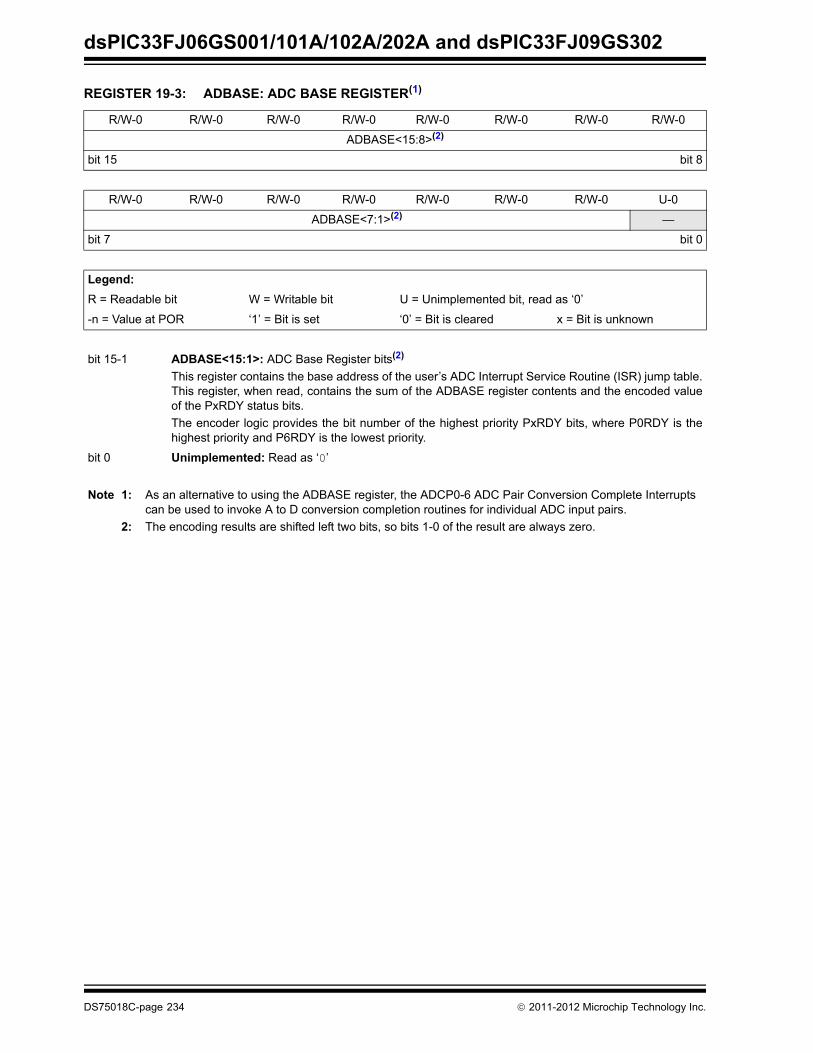
dsPIC33FJ06GS001/101A/102A/202A and dsPIC33FJ09GS302
REGISTER 19-3: ADBASE: ADC BASE REGISTER(1)
R/W-0 R/W-0 R/W-0 R/W-0 R/W-0 R/W-0 R/W-0 R/W-0
ADBASE<15:8>(2)
bit 15 bit 8
R/W-0 R/W-0 R/W-0 R/W-0 R/W-0 R/W-0 R/W-0 U-0
ADBASE<7:1>(2) —
bit 7 bit 0
Legend:
R = Readable bit W = Writable bit U = Unimplemented bit, read as ‘0’
-n = Value at POR ‘1’ = Bit is set ‘0’ = Bit is cleared x = Bit is unknown
bit 15-1 ADBASE<15:1>: ADC Base Register bits(2)
This register contains the base address of the user’s ADC Interrupt Service Routine (ISR) jump table.This register, when read, contains the sum of the ADBASE register contents and the encoded valueof the PxRDY status bits.
The encoder logic provides the bit number of the highest priority PxRDY bits, where P0RDY is thehighest priority and P6RDY is the lowest priority.
bit 0 Unimplemented: Read as ‘0’
Note 1: As an alternative to using the ADBASE register, the ADCP0-6 ADC Pair Conversion Complete Interrupts can be used to invoke A to D conversion completion routines for individual ADC input pairs.
2: The encoding results are shifted left two bits, so bits 1-0 of the result are always zero.
DS75018C-page 234 2011-2012 Microchip Technology Inc.

dsPIC33FJ06GS001/101A/102A/202A and dsPIC33FJ09GS302
REGISTER 19-4: ADPCFG: ADC PORT CONFIGURATION REGISTER
U-0 U-0 U-0 U-0 U-0 U-0 U-0 U-0
— — — — — — — —
bit 15 bit 8
R/W-0 R/W-0 U-0 U-0 R/W-0 R/W-0 R/W-0 R/W-0
PCFG7(1) PCFG6(1) — — PCFG3 PCFG2 PCFG1 PCFG0
bit 7 bit 0
Legend:
R = Readable bit W = Writable bit U = Unimplemented bit, read as ‘0’
-n = Value at POR ‘1’ = Bit is set ‘0’ = Bit is cleared x = Bit is unknown
bit 15-8 Unimplemented: Read as ‘0’
bit 7-6 PCFG<7:6>: Analog-to-Digital Port Configuration Control bits(1)
1 = Port pin is in Digital mode; port read input is enabled; Analog-to-Digital input multiplexer isconnected to AVSS
0 = Port pin is in Analog mode; port read input is disabled; Analog-to-Digital samples pin voltage
bit 5-4 Unimplemented: Read as ‘0’
bit 3-0 PCFG<3:0>: Analog-to-Digital Port Configuration Control bits
1 = Port pin is in Digital mode; port read input is enabled; Analog-to-Digital input multiplexer isconnected to AVSS
0 = Port pin is in Analog mode; port read input is disabled; Analog-to-Digital samples pin voltage
Note 1: This bit is not implemented in dsPIC33FJ06GS102A/202A devices.
2: This bit is not implemented in dsPIC33FJ06GS001/101A devices.
2011-2012 Microchip Technology Inc. DS75018C-page 235

dsPIC33FJ06GS001/101A/102A/202A and dsPIC33FJ09GS302
REGISTER 19-5: ADCPC0: ADC CONVERT PAIR CONTROL REGISTER 0
R/W-0 R/W-0 R/W-0 R/W-0 R/W-0 R/W-0 R/W-0 R/W-0
IRQEN1 PEND1 SWTRG1 TRGSRC1<4:0>
bit 15 bit 8
R/W-0 R/W-0 R/W-0 R/W-0 R/W-0 R/W-0 R/W-0 R/W-0
IRQEN0 PEND0 SWTRG0 TRGSRC0<4:0>
bit 7 bit 0
Legend:
R = Readable bit W = Writable bit U = Unimplemented bit, read as ‘0’
-n = Value at POR ‘1’ = Bit is set ‘0’ = Bit is cleared x = Bit is unknown
bit 15 IRQEN1: Interrupt Request Enable 1 bit1 = Enables IRQ generation when requested conversion of channels AN3 and AN2 is completed0 = IRQ is not generated
bit 14 PEND1: Pending Conversion Status 1 bit 1 = Conversion of channels AN3 and AN2 is pending; set when selected trigger is asserted0 = Conversion is complete
bit 13 SWTRG1: Software Trigger 1 bit1 = Starts conversion of AN3 and AN2 (if selected by the TRGSRCx bits)(1)
This bit is automatically cleared by hardware when the PEND1 bit is set.0 = Conversion has not started
bit 12-8 TRGSRC1<4:0>: Trigger 1 Source Selection bitsSelects trigger source for conversion of analog channels AN3 and AN2.11111 = Timer2 period match•••11011 = Reserved11010 = PWM Generator 4 current-limit ADC trigger11001 = Reserved11000 = PWM Generator 2 current-limit ADC trigger10111 = PWM Generator 1 current-limit ADC trigger10110 = Reserved•••10010 = Reserved10001 = PWM Generator 4 secondary trigger is selected10000 = Reserved01111 = PWM Generator 2 secondary trigger is selected01110 = PWM Generator 1 secondary trigger is selected01101 = Reserved01100 = Timer1 period match•••01000 = Reserved00111 = PWM Generator 4 primary trigger is selected00110 = Reserved00101 = PWM Generator 2 primary trigger is selected00100 = PWM Generator 1 primary trigger is selected00011 = PWM Special Event Trigger is selected00010 = Global software trigger is selected00001 = Individual software trigger is selected00000 = No conversion is enabled
Note 1: The trigger source must be set as a global software trigger prior to setting this bit to ‘1’. If other conversions are in progress, then conversion will be performed when the conversion resources are available.
DS75018C-page 236 2011-2012 Microchip Technology Inc.

dsPIC33FJ06GS001/101A/102A/202A and dsPIC33FJ09GS302
bit 7 IRQEN0: Interrupt Request Enable 0 bit
1 = Enables IRQ generation when requested conversion of channels AN1 and AN0 is completed0 = IRQ is not generated
bit 6 PEND0: Pending Conversion Status 0 bit
1 = Conversion of channels AN1 and AN0 is pending; set when selected trigger is asserted0 = Conversion is complete
bit 5 SWTRG0: Software Trigger 0 bit1 = Starts conversion of AN1 and AN0 (if selected by the TRGSRCx bits)(1)
This bit is automatically cleared by hardware when the PEND0 bit is set.0 = Conversion has not started
bit 4-0 TRGSRC0<4:0>: Trigger 0 Source Selection bitsSelects trigger source for conversion of analog channels AN1 and AN0.11111 = Timer2 period match•••11011 = Reserved11010 = PWM Generator 4 current-limit ADC trigger11001 = Reserved11000 = PWM Generator 2 current-limit ADC trigger10111 = PWM Generator 1 current-limit ADC trigger10110 = Reserved•••10010 = Reserved10001 = PWM Generator 4 secondary trigger is selected10000 = Reserved01111 = PWM Generator 2 secondary trigger is selected01110 = PWM Generator 1 secondary trigger is selected01101 = Reserved01100 = Timer1 period match•••01000 = Reserved00111 = PWM Generator 4 primary trigger is selected00110 = Reserved00101 = PWM Generator 2 primary trigger is selected00100 = PWM Generator 1 primary trigger is selected00011 = PWM Special Event Trigger is selected00010 = Global software trigger is selected00001 = Individual software trigger is selected00000 = No conversion is enabled
REGISTER 19-5: ADCPC0: ADC CONVERT PAIR CONTROL REGISTER 0 (CONTINUED)
Note 1: The trigger source must be set as a global software trigger prior to setting this bit to ‘1’. If other conversions are in progress, then conversion will be performed when the conversion resources are available.
2011-2012 Microchip Technology Inc. DS75018C-page 237

dsPIC33FJ06GS001/101A/102A/202A and dsPIC33FJ09GS302
REGISTER 19-6: ADCPC1: ADC CONVERT PAIR CONTROL REGISTER 1
R/W-0 R/W-0 R/W-0 R/W-0 R/W-0 R/W-0 R/W-0 R/W-0
IRQEN3(1) PEND3(1) SWTRG3(1) TRGSRC3<4:0>(1)
bit 15 bit 8
R/W-0 R/W-0 R/W-0 R/W-0 R/W-0 R/W-0 R/W-0 R/W-0
IRQEN2(2) PEND2(2) SWTRG2(2) TRGSRC2<4:0>(2)
bit 7 bit 0
Legend:
R = Readable bit W = Writable bit U = Unimplemented bit, read as ‘0’
-n = Value at POR ‘1’ = Bit is set ‘0’ = Bit is cleared x = Bit is unknown
bit 15 IRQEN3: Interrupt Request Enable 3 bit(1)
1 = Enables IRQ generation when requested conversion of channels AN7 and AN6 is completed0 = IRQ is not generated
bit 14 PEND3: Pending Conversion Status 3 bit(1) 1 = Conversion of channels AN7 and AN6 is pending; set when selected trigger is asserted0 = Conversion is complete
bit 13 SWTRG3: Software Trigger 3 bit(1)
1 = Starts conversion of AN7 and AN6 (if selected by the TRGSRCx bits)(3)
This bit is automatically cleared by hardware when the PEND3 bit is set.0 = Conversion has not started
bit 12-8 TRGSRC3<4:0>: Trigger 3 Source Selection bits(1)
Selects trigger source for conversion of analog channels AN7 and AN6.11111 = Timer2 period match•
•
•
11011 = Reserved11010 = PWM Generator 4 current-limit ADC trigger11001 = Reserved11000 = PWM Generator 2 current-limit ADC trigger10111 = PWM Generator 1 current-limit ADC trigger10110 = Reserved•
•
•
10010 = Reserved10001 = PWM Generator 4 secondary trigger is selected10000 = Reserved01111 = PWM Generator 2 secondary trigger is selected01110 = PWM Generator 1 secondary trigger is selected01101 = Reserved01100 = Timer1 period match•
•
•
01000 = Reserved00111 = PWM Generator 4 primary trigger is selected00110 = Reserved00101 = PWM Generator 2 primary trigger is selected00100 = PWM Generator 1 primary trigger is selected00011 = PWM Special Event Trigger is selected00010 = Global software trigger is selected00001 = Individual software trigger is selected00000 = No conversion is enabled
Note 1: This bit is available in dsPIC33FJ06GS001/101A and dsPIC33FJ09GS302 devices only.2: This bit is available in dsPIC33FJ06GS102A/201A and dsPIC33FJ09GS302 devices only.3: The trigger source must be set as a global software trigger prior to setting this bit to ‘1’. If other conversions
are in progress, conversion will be performed when the conversion resources are available.
DS75018C-page 238 2011-2012 Microchip Technology Inc.

dsPIC33FJ06GS001/101A/102A/202A and dsPIC33FJ09GS302
bit 7 IRQEN2: Interrupt Request Enable 2 bit(2)
1 = Enables IRQ generation when requested conversion of channels AN5 and AN4 is completed0 = IRQ is not generated
bit 6 PEND2: Pending Conversion Status 2 bit(2)
1 = Conversion of channels AN5 and AN4 is pending; set when selected trigger is asserted.0 = Conversion is complete
bit 5 SWTRG2: Software Trigger 2 bit(2)
1 = Starts conversion of AN5 and AN4 (if selected by the TRGSRCx bits)(3)
This bit is automatically cleared by hardware when the PEND2 bit is set.0 = Conversion has not started
bit 4-0 TRGSRC2<4:0>: Trigger 2 Source Selection bits(2)
Selects trigger source for conversion of analog channels AN5 and AN4.11111 = Timer2 period match•
•
•
11011 = Reserved11010 = PWM Generator 4 current-limit ADC trigger11001 = Reserved11000 = PWM Generator 2 current-limit ADC trigger10111 = PWM Generator 1 current-limit ADC trigger10110 = Reserved•
•
•
10010 = Reserved10001 = PWM Generator 4 secondary trigger is selected10000 = Reserved01111 = PWM Generator 2 secondary trigger is selected01110 = PWM Generator 1 secondary trigger is selected01101 = Reserved01100 = Timer1 period match•
•
•
01000 = Reserved00111 = PWM Generator 4 primary trigger is selected00110 = Reserved00101 = PWM Generator 2 primary trigger is selected00100 = PWM Generator 1 primary trigger is selected00011 = PWM Special Event Trigger is selected00010 = Global software trigger is selected00001 = Individual software trigger is selected00000 = No conversion is enabled
REGISTER 19-6: ADCPC1: ADC CONVERT PAIR CONTROL REGISTER 1 (CONTINUED)
Note 1: This bit is available in dsPIC33FJ06GS001/101A and dsPIC33FJ09GS302 devices only.2: This bit is available in dsPIC33FJ06GS102A/201A and dsPIC33FJ09GS302 devices only.3: The trigger source must be set as a global software trigger prior to setting this bit to ‘1’. If other conversions
are in progress, conversion will be performed when the conversion resources are available.
2011-2012 Microchip Technology Inc. DS75018C-page 239

dsPIC33FJ06GS001/101A/102A/202A and dsPIC33FJ09GS302
REGISTER 19-7: ADCPC3: ADC CONVERT PAIR CONTROL REGISTER 3(1)
U-0 U-0 U-0 U-0 U-0 U-0 U-0 U-0
— — — — — — — —
bit 15 bit 8
R/W-0 R/W-0 R/W-0 R/W-0 R/W-0 R/W-0 R/W-0 R/W-0
IRQEN6 PEND6 SWTRG6 TRGSRC6<4:0>
bit 7 bit 0
Legend:
R = Readable bit W = Writable bit U = Unimplemented bit, read as ‘0’
-n = Value at POR ‘1’ = Bit is set ‘0’ = Bit is cleared x = Bit is unknown
bit 15-8 Unimplemented: Read as ‘0’
bit 7 IRQEN6: Interrupt Request Enable 6 bit
1 = Enable IRQ generation when requested conversion of channels AN13 and AN12 is completed0 = IRQ is not generated
bit 6 PEND6: Pending Conversion Status 6 bit1 = Conversion of channels AN13 and AN 12 is pending; set when selected trigger is asserted0 = Conversion is complete
bit 5 SWTRG6: Software Trigger 6 bit
1 = Starts conversion of AN13 (INTREF) and AN12 (EXTREF) if selected by TRGSRC bits(2)
This bit is automatically cleared by hardware when the PEND6 bit is set.0 = Conversion has not started
Note 1: If other conversions are in progress, conversion will be performed when the conversion resources are available.
2: AN13 is internally connected to Vref in all devices. AN12 is internally connected to the EXTREF pin in the dsPIC33FJ06001/202A and dsPIC33FJ09GS302 devices. The dsPIC33FJ06GS101A/102A devices not have an EXTREF pin; therefore, any data read on the corresponding AN12 input will be invalid.
DS75018C-page 240 2011-2012 Microchip Technology Inc.
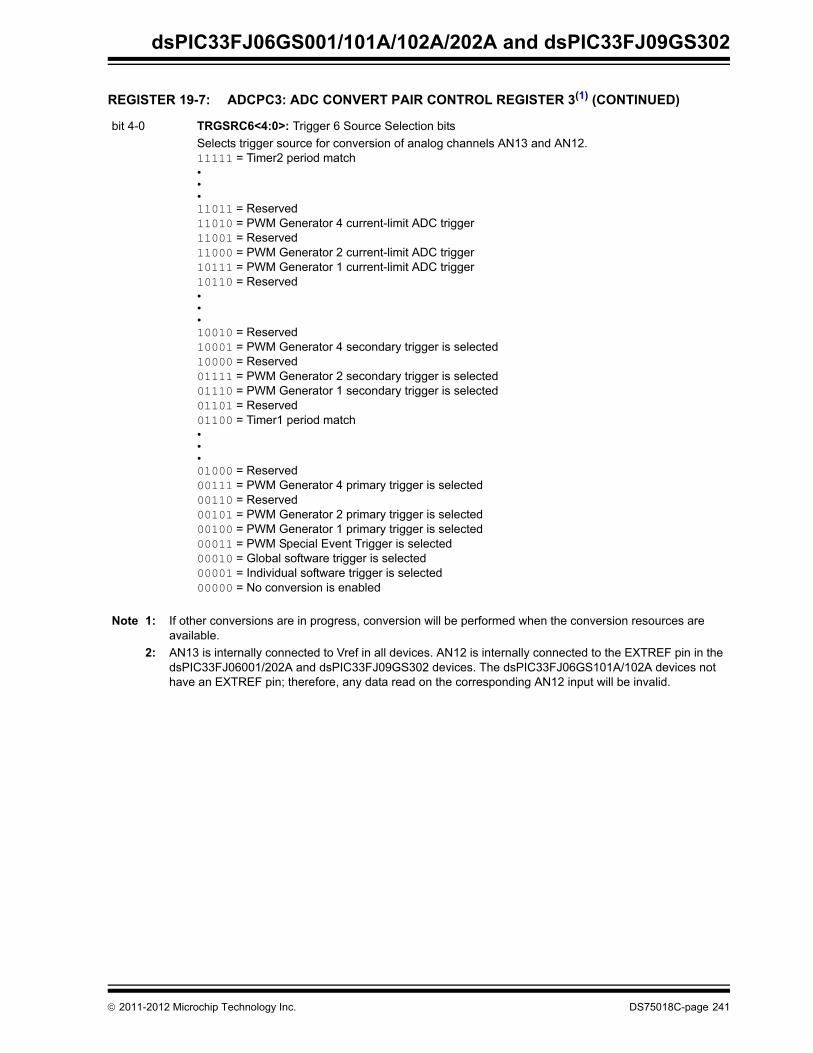
dsPIC33FJ06GS001/101A/102A/202A and dsPIC33FJ09GS302
bit 4-0 TRGSRC6<4:0>: Trigger 6 Source Selection bits
Selects trigger source for conversion of analog channels AN13 and AN12.11111 = Timer2 period match•••11011 = Reserved11010 = PWM Generator 4 current-limit ADC trigger11001 = Reserved11000 = PWM Generator 2 current-limit ADC trigger10111 = PWM Generator 1 current-limit ADC trigger10110 = Reserved•••10010 = Reserved10001 = PWM Generator 4 secondary trigger is selected10000 = Reserved01111 = PWM Generator 2 secondary trigger is selected01110 = PWM Generator 1 secondary trigger is selected01101 = Reserved01100 = Timer1 period match•••01000 = Reserved00111 = PWM Generator 4 primary trigger is selected00110 = Reserved00101 = PWM Generator 2 primary trigger is selected00100 = PWM Generator 1 primary trigger is selected00011 = PWM Special Event Trigger is selected00010 = Global software trigger is selected00001 = Individual software trigger is selected00000 = No conversion is enabled
REGISTER 19-7: ADCPC3: ADC CONVERT PAIR CONTROL REGISTER 3(1) (CONTINUED)
Note 1: If other conversions are in progress, conversion will be performed when the conversion resources are available.
2: AN13 is internally connected to Vref in all devices. AN12 is internally connected to the EXTREF pin in the dsPIC33FJ06001/202A and dsPIC33FJ09GS302 devices. The dsPIC33FJ06GS101A/102A devices not have an EXTREF pin; therefore, any data read on the corresponding AN12 input will be invalid.
2011-2012 Microchip Technology Inc. DS75018C-page 241

dsPIC33FJ06GS001/101A/102A/202A and dsPIC33FJ09GS302
NOTES:
DS75018C-page 242 2011-2012 Microchip Technology Inc.

dsPIC33FJ06GS001/101A/102A/202A and dsPIC33FJ09GS302
20.0 HIGH-SPEED ANALOG COMPARATOR
The high-speed analog comparator module monitorscurrent and/or voltage transients that may be too fastfor the CPU and ADC to capture.
20.1 Features Overview
The SMPS comparator module offers the followingmajor features:
• Eight selectable comparator inputs
• Up to two analog comparators
• 10-bit DAC for each analog comparator
• Programmable output polarity
• Interrupt generation capability
• DACOUT pin to provide DAC output
• DACOUT amplifier (1x, 1.8x)
• Selectable hysteresis
• DAC has three ranges of operation:
- AVDD/2
- Internal Reference (INTREF)
- External Reference (EXTREF)
• ADC sample and convert trigger capability
• Disable capability reduces power consumption
• Functional support for PWM module:
- PWM duty cycle control
- PWM period control
- PWM Fault detect
20.2 Module Description
Figure 20-1 shows a functional block diagram of oneanalog comparator from the high-speed analogcomparator module. The analog comparator provideshigh-speed operation with a typical delay of 20 ns. Thecomparator has a typical offset voltage of ±5 mV. Thenegative input of the comparator is always connectedto the DAC circuit. The positive input of the comparatoris connected to an analog multiplexer that selects thedesired source pin.
The analog comparator input pins are typically sharedwith pins used by the Analog-to-Digital Converter(ADC) module. Both the comparator and the ADC canuse the same pins at the same time. This capabilityenables a user to measure an input voltage with theADC and detect voltage transients with thecomparator.
FIGURE 20-1: HIGH-SPEED ANALOG COMPARATOR MODULE BLOCK DIAGRAM
Note 1: This data sheet summarizes the featuresof the dsPIC33FJ06GS001/101A/102A/202A and dsPIC33FJ09GS302 familiesof devices. It is not intended to be acomprehensive reference source. Tocomplement the information in this datasheet, refer to Section 45. “High-SpeedAnalog Comparator” (DS70296) in the“dsPIC33F/PIC24H Family ReferenceManual”, which is available on theMicrochip web site (www.microchip.com).
2: Some registers and associated bitsdescribed in this section may not beavailable on all devices. Refer toSection 4.0 “Memory Organization” inthis data sheet for device-specific registerand bit information.
CMPxA(1)
CMPxC(1)
DAC
CMPPOL
0
1
AVDD/2
INTREF(2)
MUX
MUX
CMREF
CMPx(1)
INSEL<1:0>
10
Interrupt Request
CMPxB(1)
CMPxD(1)
Pulse Stretcher
EXTREF(2)
Trigger to PWM
AVSS
and
RANGE
DACOUT
DACOE
Note 1: x = 1 and 2.2: For the INTREF and EXTREF values, refer to the DAC Module Specifications (Table 25-42) in Section 25.0
“Electrical Characteristics”.3: The output buffer is shared between the DACs and only one DAC can be enabled to drive this buffer.
StatusDigital Filter
HGAINOutputBuffer(3)
AMP
2011-2012 Microchip Technology Inc. DS75018C-page 243

dsPIC33FJ06GS001/101A/102A/202A and dsPIC33FJ09GS302
20.3 Module Applications
This module provides a means for the SMPS dsPICDSC devices to monitor voltage and currents in apower conversion application. The ability to detecttransient conditions and stimulate the dsPIC DSCprocessor and/or peripherals, without requiring theprocessor and ADC to constantly monitor voltages orcurrents, frees the dsPIC DSC to perform other tasks.
The comparator module has a high-speed comparator,an associated 10-bit DAC and a DAC output amplifierthat provide a programmable reference voltage to theinverting input of the comparator. The polarity of thecomparator output is user-programmable. The outputof the module can be used in the following modes:
• Generate an Interrupt
• Trigger an ADC Sample and Convert Process
• Truncate the PWM Signal (current limit)
• Truncate the PWM Period (current minimum)
• Disable the PWM Outputs (Fault latch)
The output of the comparator module may be used inmultiple modes at the same time, such as: 1) generatean interrupt, 2) have the ADC take a sample and con-vert it, and 3) truncate the PWM output in response toa voltage being detected beyond its expected value.
The comparator module can also be used to wake-upthe system from Sleep or Idle mode when the analoginput voltage exceeds the programmed thresholdvoltage.
20.4 DAC
The range of the DAC is controlled via an analogmultiplexer that selects either AVDD/2, an internalreference source, INTREF, or an external referencesource, EXTREF. The full range of the DAC (AVDD/2)will typically be used when the chosen input source pinis shared with the ADC. The reduced range option(INTREF) will likely be used when monitoring currentlevels using a current sense resistor. Usually, themeasured voltages in such applications are small(<1.25V); therefore, the option of using a reducedreference range for the comparator extends theavailable DAC resolution in these applications. Theuse of an external reference enables the user toconnect to a reference that better suits theirapplication.
DACOUT, shown in Figure 20-1, can only beassociated with a single comparator at a given time.
20.5 DAC Buffer Gain
The output of the DAC is buffered/amplified via theDAC buffer. The block functions as a 1x gain amplifieror as a 1.8x gain amplifier. The gain selection is con-trolled via the HGAIN bit in the CMPCONx register.Using the 1.8x gain option will raise the referencevoltage to the analog comparator to a maximum of2.8V. Using a higher reference voltage for the analogcomparator can improve the signal-to-noise ratio in anapplication.
20.6 Comparator Input Range
The comparator has an input voltage range from -0.2Vto AVDD + 0.2V, making it a rail-to-rail input.
20.7 Digital Logic
The CMPCONx register (see Register 20-1) providesthe control logic that configures the High-Speed AnalogComparator module. The digital logic provides a pulsestretcher. The analog comparator can respond to veryfast transient signals. After the comparator output isgiven the desired polarity, the signal is passed to thispulse stretching circuit. The pulse stretching circuit hasan asynchronous set function and a delay circuit thatinsure the minimum pulse width is three system clockcycles wide so that the attached circuitry can properlyrespond.
The stretch circuit is followed by a digital filter. Thedigital filter is enabled via the FLTREN bit in theCMPCONx register. The digital filter operates with theclock specified via the FCLKSEL bit in the CMPCONxregister. The comparator signal must be stable in a highor low state for at least three of the selected clockcycles for it to pass through the digital filter.
During Sleep mode, the clock signal inputs to themodule are disabled. However, the module’s analogcomponents may continue to function in a reducedpower manner to allow the user to wake-up the devicewhen a signal is applied to a comparator input.
In Sleep mode, the clocks are stopped; however, theanalog comparator signal has an asynchronous con-nection across the filter that allows interrupts to begenerated regardless of the stopped clocks.
The comparator can be disabled while in Idle mode ifthe CMPSIDL bit is set. If a device has multiple compar-ators, and any CMPSIDL bit is set, the entire group ofcomparators will be disabled while in Idle mode. Theadvantage is reduced power consumption. Moreover,this behavior reduces complexity in the design of theclock control logic for this module.
Note: It should be ensured in software thatmultiple DACOE bits are not set. Theoutput on the DACOUT pin will be indeter-minate if multiple comparators enable theDAC output.
DS75018C-page 244 2011-2012 Microchip Technology Inc.

dsPIC33FJ06GS001/101A/102A/202A and dsPIC33FJ09GS302
20.8 Hysteresis
An additional feature of the module is hysteresis con-trol. Hysteresis can be enabled or disabled and itsamplitude can be controlled by the HYSSEL<1:0> bitsin the CMPCONx register. Three different values areavailable: 15 mV, 30 mV and 45 mV. It is also possibleto select the edge (rising or falling) to which hysteresisis to be applied.
Hysteresis control prevents the comparator output fromcontinuously changing state because of smallperturbations (noise) at the input (see Figure 20-2).
FIGURE 20-2: HYSTERESIS CONTROL
20.9 Interaction with I/O Buffers
If the module is enabled and a pin has been selectedas the source for the comparator, then the chosen I/Opad must disable the digital input buffer associatedwith the pad to prevent excessive currents in the digitalbuffer due to analog input voltages.
20.10 DAC Output Range
The DAC has a limitation for the maximum referencevoltage input of (AVDD – 1.5) volts. An externalreference voltage input should not exceed this value orthe reference DAC output will become indeterminate.
20.11 Analog Comparator Registers
The high-speed analog comparator module iscontrolled by the following registers:
• CMPCONx: Comparator Control x Register• CMPDACx: Comparator DAC Control x Register
Output
Input
Hysteresis Range(15 mV/30 mV/45 mV)
2011-2012 Microchip Technology Inc. DS75018C-page 245

dsPIC33FJ06GS001/101A/102A/202A and dsPIC33FJ09GS302
REGISTER 20-1: CMPCONx: COMPARATOR CONTROL x REGISTER
R/W-0 U-0 R/W-0 R/W-0 R/W-0 R/W-0 R/W-0 R/W-0
CMPON(1) — CMPSIDL(1) HYSSEL<1:0>(1) FLTREN(1) FCLKSEL(1) DACOE(1)
bit 15 bit 8
R/W-0 R/W-0 R/W-0 R/W-0 R/W-0 R/W-0 R/W-0 R/W-0
INSEL<1:0>(1) EXTREF(1) HYSPOL(1) CMPSTAT(1) HGAIN(1) CMPPOL(1) RANGE(1)
bit 7 bit 0
Legend:
R = Readable bit W = Writable bit U = Unimplemented bit, read as ‘0’
-n = Value at POR ‘1’ = Bit is set ‘0’ = Bit is cleared x = Bit is unknown
bit 15 CMPON: Comparator Operating Mode bit(1)
1 = Comparator module is enabled0 = Comparator module is disabled (reduces power consumption)
bit 14 Unimplemented: Read as ‘0’
bit 13 CMPSIDL: Stop in Idle Mode bit(1)
1 = Discontinues module operation when device enters Idle mode.0 = Continues module operation in Idle modeIf a device has multiple comparators, any CMPSIDL bit that is set to ‘1’ disables all comparators whilein Idle mode.
bit 12-11 HYSSEL<1:0>: Comparator Hysteresis Select bits(1)
11 = 45 mV hysteresis10 = 30 mV hysteresis01 = 15 mV hysteresis00 = No hysteresis is selected
bit 10 FLTREN: Digital Filter Enable bit(1)
1 = Digital filter is enabled0 = Digital filter is disabled
bit 9 FCLKSEL: Digital Filter and Pulse Stretcher Clock Select bit(1)
1 = Digital filter and pulse stretcher operate with the PWM clock0 = Digital filter and pulse stretcher operate with the system clock
bit 8 DACOE: DAC Output Enable(1)
1 = DAC analog voltage is output to DACOUT pin(2)
0 = DAC analog voltage is not connected to DACOUT pin
bit 7-6 INSEL<1:0>: Input Source Select for Comparator bits(1)
11 = Select CMPxD input pin10 = Select CMPxC input pin01 = Select CMPxB input pin00 = Select CMPxA input pin
Note 1: This bit is not implemented in dsPIC33FJ06GS101A/102A devices.
2: DACOUT can be associated only with a single comparator at any given time. The software must ensure that multiple comparators do not enable the DAC output by setting their respective DACOE bit.
3: For the INTREF value, refer to the DAC Module Specifications (Table 25-42) in Section 25.0 “Electrical Characteristics”.
DS75018C-page 246 2011-2012 Microchip Technology Inc.

dsPIC33FJ06GS001/101A/102A/202A and dsPIC33FJ09GS302
bit 5 EXTREF: Enable External Reference bit(1)
1 = External source provides reference to DAC (maximum DAC voltage determined by externalvoltage source)
0 = Internal reference sources provide reference to DAC (maximum DAC voltage determined byRANGE bit setting)
bit 4 HYSPOL: Comparator Hysteresis Polarity Select bit(1)
1 = Hysteresis is applied to the falling edge of the comparator output0 = Hysteresis is applied to the rising edge of the comparator output
bit 3 CMPSTAT: Current State of Comparator Output Including CMPPOL Selection bit(1)
bit 2 HGAIN: DAC Gain Enable bit(1)
1 = Reference DAC output to comparator is scaled at 1.8x0 = Reference DAC output to comparator is scaled at 1.0x
bit 1 CMPPOL: Comparator Output Polarity Control bit(1)
1 = Output is inverted0 = Output is non-inverted
bit 0 RANGE: Selects DAC Output Voltage Range bit(1)
1 = High Range: Max DAC Value = AVDD/2, 1.65V at 3.3V AVDD
0 = Low Range: Max DAC Value = INTREF(3)
REGISTER 20-1: CMPCONx: COMPARATOR CONTROL x REGISTER (CONTINUED)
Note 1: This bit is not implemented in dsPIC33FJ06GS101A/102A devices.
2: DACOUT can be associated only with a single comparator at any given time. The software must ensure that multiple comparators do not enable the DAC output by setting their respective DACOE bit.
3: For the INTREF value, refer to the DAC Module Specifications (Table 25-42) in Section 25.0 “Electrical Characteristics”.
2011-2012 Microchip Technology Inc. DS75018C-page 247

dsPIC33FJ06GS001/101A/102A/202A and dsPIC33FJ09GS302
REGISTER 20-2: CMPDACx: COMPARATOR DAC CONTROL x REGISTER
U-0 U-0 U-0 U-0 U-0 U-0 R/W-0 R/W-0
— — — — — — CMREF<9:8>(1)
bit 15 bit 8
R/W-0 R/W-0 R/W-0 R/W-0 R/W-0 R/W-0 R/W-0 R/W-0
CMREF<7:0>(1)
bit 7 bit 0
Legend:
R = Readable bit W = Writable bit U = Unimplemented bit, read as ‘0’
-n = Value at POR ‘1’ = Bit is set ‘0’ = Bit is cleared x = Bit is unknown
bit 15-10 Unimplemented: Read as ‘0’
bit 9-0 CMREF<9:0>: Comparator Reference Voltage Select bits(1)
1111111111 = (CMREF * INTREF/1024) or (CMREF * (AVDD/2)/1024) volts depending on RANGEbit or (CMREF * EXTREF/1024) if EXTREF is set
•
•
•
0000000000 = 0.0 volts
Note 1: These bits are not implemented in dsPIC33FJ06GS101A/102A devices.
DS75018C-page 248 2011-2012 Microchip Technology Inc.

dsPIC33FJ06GS001/101A/102A/202A and dsPIC33FJ09GS302
21.0 CONSTANT CURRENT SOURCE
The constant current source module is a precisioncurrent generator and is used in conjunction with ADCto measure the resistance of external resistorsconnected to device pins.
21.1 Features Overview
The constant current source module offers the followingmajor features:
• Constant current generator (10 µA nominal)
• Internal selectable connection to one out of four pins
• Enable/disable bit
21.2 Module Description
Figure 21-1 shows a functional block diagram of theconstant current source module. It consists of aprecision current generator with a nominal value of10 µA. The module can be enabled and disabled usingthe ISRCEN bit in the ISRCCON register. The outputof the current generator is internally connected to oneout of up to 4 pins. The OUTSEL<2:0> bits in theISRCCON register allow selection of the target pin.
The current source is calibrated during testing.
FIGURE 21-1: CONSTANT CURRENT SOURCE MODULE BLOCK DIAGRAM
Note 1: This data sheet summarizes the featuresof the dsPIC33FJ06GS001/101A/102A/202A and dsPIC33FJ09GS302 familiesof devices. It is not intended to be acomprehensive reference source. Tocomplement the information in thisdata sheet, refer to Section 19.“Inter-Integrated Circuit (I2C™)”(DS70195) in the “dsPIC33F/PIC24HFamily Reference Manual”, which isavailable on the Microchip web site(www.microchip.com).
2: Some registers and associated bitsdescribed in this section may not beavailable on all devices. Refer toSection 4.0 “Memory Organization” inthis data sheet for device-specific registerand bit information.
ISRC1
ISRC3
MUX
OUTSEL<2:0>
ISRC2
ISRC4
ISRCEN
Constant Current Source
2011-2012 Microchip Technology Inc. DS75018C-page 249

dsPIC33FJ06GS001/101A/102A/202A and dsPIC33FJ09GS302
21.3 Current Source Control Register
REGISTER 21-1: ISRCCON: CONSTANT CURRENT SOURCE CONTROL REGISTER(1)
R/W-0 U-0 U-0 U-0 U-0 R/W-0 R/W-0 R/W-0
ISRCEN — — — — OUTSEL<2:0>
bit 15 bit 8
U-0 U-0 R-0 R-0 R-0 R-0 R-0 R-0
— — ISRCCAL<5:0>
bit 7 bit 0
Legend:
R = Readable bit W = Writable bit U = Unimplemented bit, read as ‘0’
-n = Value at POR ‘1’ = Bit is set ‘0’ = Bit is cleared x = Bit is unknown
bit 15 ISRCEN: Current Source Enable bit
1 = Current source is enabled0 = Current source is disabled
bit 14-11 Unimplemented: Read as ‘0’
bit 10-8 OUTSEL<2:0>: Output Current Select bits
111 = Reserved110 = Reserved101 = Reserved100 = Select input pin, ISRC4 (AN4)011 = Select input pin, ISRC3 (AN5)010 = Select input pin, ISRC2 (AN6)001 = Select input pin, ISRC1 (AN7)000 = No output is selected
bit 7-6 Unimplemented: Read as ‘0’
bit 5-0 ISRCCAL<5:0>: Current Source Calibration bits
The calibration value must be copied from Flash address, 0x800840, into these bits. Refer to the Constant Current Source Calibration Register (Register 22-1) in Section 22.0 “Special Features” for more information.
Note 1: This register is available in the dsPIC33FJ09GS302 device only.
DS75018C-page 250 2011-2012 Microchip Technology Inc.

dsPIC33FJ06GS001/101A/102A/202A and dsPIC33FJ09GS302
22.0 SPECIAL FEATURES
The dsPIC33FJ06GS001/101A/102A/202A anddsPIC33FJ09GS302 family of devices includes severalfeatures that are included to maximize applicationflexibility and reliability, and minimize cost throughelimination of external components. These features are:
• Flexible Configuration• Watchdog Timer (WDT)• Code Protection• JTAG Boundary Scan Interface• In-Circuit Serial Programming™ (ICSP™)• In-Circuit Emulation• Brown-out Reset (BOR)
22.1 Configuration Bits
The configuration bytes are implemented as volatilememory. This means that configuration data must beprogrammed each time the device is powered up. Con-figuration data is stored in the words at the top of theon-chip program memory space, known as the FlashConfiguration Words. Their specific locations areshown in Table 22-1 and Table 22-2. The configurationdata is automatically loaded from the Flash Configura-tion Words to the proper Configuration registers duringdevice Resets.
When creating applications for these devices, usersshould always specifically allocate the location of theFlash Configuration byte for configuration data. This isto make certain that program code is not stored in thisaddress when the code is compiled.
The upper 2 bytes of all Flash Configuration Words inprogram memory should always be ‘1111 1111 11111111’. This makes them appear to be NOP instructionsin the remote event that their locations are ever exe-cuted by accident. Since Configuration bits are notimplemented in the corresponding locations, writing‘1’s to these locations has no effect on deviceoperation.
The Configuration Flash Byte maps are shown inTable 22-1 and Table 22-2.
The Constant Current Source Calibration register isshown in Register 22-1.
Note 1: This data sheet summarizes the featuresof the dsPIC33FJ06GS001/101A/102A/202A and dsPIC33FJ09GS302 devices.It is not intended to be a comprehensivereference source. To complement theinformation in this data sheet, refer toSection 24. “Programming and Diag-nostics” (DS70207) and Section 25.“Device Configuration” (DS70194)in the “dsPIC33F/PIC24H FamilyReference Manual”, which are avail-able from the Microchip web site(www.microchip.com).
2: Some registers and associated bitsdescribed in this section may not beavailable on all devices. Refer toSection 4.0 “Memory Organization” inthis data sheet for device-specific registerand bit information.
Note: Configuration data is reloaded on all typesof device Resets.
Note: Performing a page erase operation on thelast page of program memory, clears theFlash Configuration Words, enabling codeprotection as a result. Therefore, usersshould avoid performing page eraseoperations on the last page of programmemory
2011-2012 Microchip Technology Inc. DS75018C-page 251

dsP
IC33F
J06GS
001/101A/102A
/202A an
d d
sPIC
33FJ09G
S302
DS
75018C-page 252
2011-2012 M
icrochip Technolo
gy Inc.
Bit 2 Bit 1 Bit 0
— ICS<1:0>
WDTPOST<3:0>
OSCIOFNC POSCMD<1:0>
FNOSC<2:0>
— GCP GWRP
Bit 2 Bit 1 Bit 0
— ICS<1:0>
WDTPOST<3:0>
OSCIOFNC POSCMD<1:0>
FNOSC<2:0>
— GCP GWRP
TABLE 22-1: CONFIGURATION FLASH BYTES FOR dsPIC33FJ06GS001/101A/X02A DEVICES
Address Name Bits 23-8 Bit 7 Bit 6 Bit 5 Bit 4 Bit 3
000FF0 FICD — Reserved(1) — JTAGEN Reserved(2) —
000FF4 FWDT — FWDTEN — PLLKEN WDTPRE
000FF6 FOSC — FCKSM<1:0> IOL1WAY — —
000FF8 FOSCSEL — IESO — — — —
000FFA FGS — — — — — —
Legend: — = unimplemented, read as ‘1’.Note 1: This bit is reserved for use by development tools.
2: This bit is reserved; program as ‘0’.
TABLE 22-2: CONFIGURATION FLASH BYTES FOR dsPIC33FJ09GS302 DEVICES
Address Name Bits 23-8 Bit 7 Bit 6 Bit 5 Bit 4 Bit 3
0017F0 FICD — Reserved(1) — JTAGEN Reserved(2) —
0017F4 FWDT — FWDTEN — PLLKEN WDTPRE
0017F6 FOSC — FCKSM<1:0> IOL1WAY — —
0017F8 FOSCSEL — IESO — — — —
0017FA FGS — — — — — —
Legend: — = unimplemented, read as ‘1’.Note 1: This bit is reserved for use by development tools.
2: This bit is reserved; program as ‘0’.

dsPIC33FJ06GS001/101A/102A/202A and dsPIC33FJ09GS302
REGISTER 22-1: CONSTANT CURRENT SOURCE CALIBRATION REGISTER
U-0 U-0 U-0 U-0 U-0 U-0 U-0 U-0
— — — — — — — —
bit 23 bit 16
U-0 U-0 U-0 U-0 U-0 U-0 U-0 U-0
— — — — — — — —
bit 15 bit 8
U-0 U-0 R-0 R-0 R-0 R-0 R-0 R-0
— — CCSCAL<5:0>
bit 7 bit 0
Legend:
R = Readable bit W = Writable bit U = Unimplemented bit, read as ‘0’
-n = Value at POR ‘1’ = Bit is set ‘0’ = Bit is cleared x = Bit is unknown
bit 23-6 Unimplemented: Read as ‘0’
bit 5-0 CCSCAL<5:0>: Constant Current Source Calibration bits
The value of these bits must be copied into the ISRCCAL<5:0> bits (ISRCCON<5:0>). Refer to the Current Source Control register (Register 21-1) in Section 21.0 “Constant Current Source”.
2011-2012 Microchip Technology Inc. DS75018C-page 253

dsPIC33FJ06GS001/101A/102A/202A and dsPIC33FJ09GS302
TABLE 22-3: dsPIC33F CONFIGURATION BITS DESCRIPTION
Bit Field Description
GCP General Segment Code-Protect bit
1 = User program memory is not code-protected0 = Code protection is enabled for the entire program memory space
GWRP General Segment Write-Protect bit
1 = User program memory is not write-protected0 = User program memory is write-protected
IESO Two-Speed Oscillator Start-up Enable bit
1 = Start up device with FRC, then automatically switch to the user-selected oscillator sourcewhen ready
0 = Start up device with user-selected oscillator source
FNOSC<2:0> Oscillator Selection bits
111 = Fast RC Oscillator with divide-by-N (FRCDIVN)110 = Reserved; do not use101 = Low-Power RC Oscillator (LPRC)100 = Reserved; do not use011 = Primary Oscillator with PLL module (MS + PLL, EC + PLL)010 = Primary Oscillator (MS, HS, EC)001 = Fast RC Oscillator with divide-by-N with PLL module
(FRCDIVN + PLL)000 = Fast RC Oscillator (FRC)
FCKSM<1:0> Clock Switching Mode bits
1x = Clock switching is disabled, Fail-Safe Clock Monitor is disabled01 = Clock switching is enabled, Fail-Safe Clock Monitor is disabled00 = Clock switching is enabled, Fail-Safe Clock Monitor is enabled
IOL1WAY Peripheral Pin Select Configuration bit
1 = Allow only one reconfiguration0 = Allow multiple reconfigurations
OSCIOFNC OSC2 Pin Function bit (except in MS and HS modes)
1 = OSC2 is the clock output0 = OSC2 is the general purpose digital I/O pin
POSCMD<1:0> Primary Oscillator Mode Select bits
11 = Primary Oscillator is disabled10 = HS Crystal Oscillator mode (10 MHz-32 MHz)01 = MS Crystal Oscillator mode (3 MHz-10 MHz)00 = EC (External Clock) mode (DC-32 MHz)
FWDTEN Watchdog Timer Enable bit
1 = Watchdog Timer is always enabled (LPRC oscillator cannot be disabled; clearing the SWDTENbit in the RCON register will have no effect)
0 = Watchdog Timer is enabled/disabled by user software (LPRC can be disabled by clearingthe SWDTEN bit in the RCON register)
WDTPRE Watchdog Timer Prescaler bit
1 = 1:1280 = 1:32
WDTPOST<3:0> Watchdog Timer Postscaler bits
1111 = 1:32,7681110 = 1:16,384•••0001 = 1:20000 = 1:1
DS75018C-page 254 2011-2012 Microchip Technology Inc.

dsPIC33FJ06GS001/101A/102A/202A and dsPIC33FJ09GS302
PLLKEN PLL Lock Enable bit
1 = Clock switch to PLL source will wait until the PLL lock signal is valid0 = Clock switch will not wait for the PLL lock signal
JTAGEN JTAG Enable bit
1 = JTAG is enabled0 = JTAG is disabled
ICS<1:0> ICD Communication Channel Select bits
11 = Communicate on PGEC1 and PGED110 = Communicate on PGEC2 and PGED201 = Communicate on PGEC3 and PGED300 = Reserved, do not use
TABLE 22-3: dsPIC33F CONFIGURATION BITS DESCRIPTION (CONTINUED)
Bit Field Description
2011-2012 Microchip Technology Inc. DS75018C-page 255

dsPIC33FJ06GS001/101A/102A/202A and dsPIC33FJ09GS302
22.2 On-Chip Voltage Regulator
The devices power their core digital logic at a nominal2.5V. This can create a conflict for designs that arerequired to operate at a higher typical voltage, such as3.3V. To simplify system design, all devices incorporatean on-chip regulator that allows the device to run its corelogic from VDD.
The regulator provides power to the core from the otherVDD pins. When the regulator is enabled, a low-ESR(less than 5 ohms) capacitor (such as tantalum orceramic) must be connected to the VCAP pin(Figure 22-1). This helps to maintain the stability of theregulator. The recommended value for the filtercapacitor is provided in Table 25-13, located inSection 25.1 “DC Characteristics”.
On a POR, it takes approximately 20 s for the on-chipvoltage regulator to generate an output voltage. Duringthis time, designated as TSTARTUP, code execution isdisabled. TSTARTUP is applied every time the deviceresumes operation after any power-down.
FIGURE 22-1: CONNECTIONS FOR THE ON-CHIP VOLTAGE REGULATOR(1,2,3)
22.3 Brown-out Reset (BOR)
The Brown-out Reset (BOR) module is based on aninternal voltage reference circuit. The main purpose ofthe BOR module is to generate a device Reset when abrown-out condition occurs. Brown-out conditions aregenerally caused by glitches on the AC mains (forexample, missing portions of the AC cycle waveformdue to bad power transmission lines or voltage sagsdue to excessive current draw when a large inductiveload is turned on).
A BOR generates a Reset pulse which resets thedevice. The BOR selects the clock source, based onthe device Configuration bit values (FNOSC<2:0> andPOSCMD<1:0>).
If an oscillator mode is selected, the BOR activates theOscillator Start-up Timer (OST). The system clock isheld until the OST expires. If the PLL is used, the clockis held until the LOCK bit (OSCCON<5>) is ‘1’.
Concurrently, the PWRT time-out (TPWRT) is appliedbefore the internal Reset is released. If TPWRT = 0 anda crystal oscillator is being used, then a nominal delayof, TFSCM = 100, is applied. The total delay in this caseis TFSCM.
The BOR status bit (RCON<1>) is set to indicate that aBOR has occurred. The BOR circuit continues tooperate while in Sleep or Idle modes and resets thedevice should VDD fall below the BOR thresholdvoltage.
Note: It is important for the low-ESR capacitor to beplaced as close as possible to the VCAP pin.
Note 1: These are typical operating voltages. Refer to Table 25-13 located in Section 25.1 “DC Characteristics” for the full operating ranges of VDD.
2: It is important for the low-ESR capacitor to be placed as close as possible to the VCAP pin.
3: Typical VCAP pin voltage = 2.5V when VDD VDDMIN.
VDD
VCAP
VSS
dsPIC33F
CEFC
3.3V
10 µFTantalum
DS75018C-page 256 2011-2012 Microchip Technology Inc.

dsPIC33FJ06GS001/101A/102A/202A and dsPIC33FJ09GS302
22.4 Watchdog Timer (WDT)
The Watchdog Timer (WDT) is driven by the LPRCoscillator. When the WDT is enabled, the clock source isalso enabled.
22.4.1 PRESCALER/POSTSCALER
The nominal WDT clock source from LPRC is 32 kHz.This feeds a prescaler that can be configured for either5-bit (divide-by-32) or 7-bit (divide-by-128) operation.The prescaler is set by the WDTPRE Configuration bit(FWDT<4>). With a 32 kHz input, the prescaler yieldsa nominal WDT time-out period (TWDT) of 1 ms in 5-bitmode or 4 ms in 7-bit mode.
A variable postscaler divides down the WDT prescaleroutput and allows for a wide range of time-out periods.The postscaler is controlled by the WDTPOST<3:0>Configuration bits (FWDT<3:0>), which allow theselection of 16 settings, from 1:1 to 1:32,768. Using theprescaler and postscaler, time-out periods ranging from1 ms to 131 seconds can be achieved.
The WDT, prescaler and postscaler are reset:
• On any device Reset
• On the completion of a clock switch, whether invoked by software (i.e., setting the OSWEN bit after changing the NOSC<2:0> bits) or by hardware (i.e., Fail-Safe Clock Monitor)
• When a PWRSAV instruction is executed (i.e., Sleep or Idle mode is entered)
• When the device exits Sleep or Idle mode to resume normal operation
• By a CLRWDT instruction during normal execution
22.4.2 SLEEP AND IDLE MODES
If the WDT is enabled, it will continue to run duringSleep or Idle modes. When the WDT time-out occurs,the device will wake the device and code execution willcontinue from where the PWRSAV instruction wasexecuted. The corresponding SLEEP bit (RCON<3>)or IDLE bit (RCON<2>) will need to be cleared insoftware after the device wakes up.
22.4.3 ENABLING WDT
The WDT is enabled or disabled by the FWDTENConfiguration bit in the FWDT Configuration register(FWDT<7>). When the FWDTEN Configuration bit isset, the WDT is always enabled.
The WDT can be optionally controlled in software whenthe FWDTEN Configuration bit has been programmedto ‘0’. The WDT is enabled in software by setting theSWDTEN control bit (RCON<5>). The SWDTENcontrol bit is cleared on any device Reset. The softwareWDT option allows the user application to enable theWDT for critical code segments and disable the WDTduring non-critical segments for maximum powersavings.
The WDT flag bit, WDTO (RCON<4>), is not automaticallycleared following a WDT time-out. To detect subsequentWDT events, the flag must be cleared in software.
FIGURE 22-2: WDT BLOCK DIAGRAM
Note: The CLRWDT and PWRSAV instructionsclear the prescaler and postscaler countswhen executed.
0
1
WDTPRE WDTPOST<3:0>
Watchdog Timer
Sleep/Idle
WDT
WDT Window Select
WDT
CLRWDT Instruction
SWDTEN
FWDTEN
LPRC Clock
Wake-up
Reset
All Device ResetsTransition to New Clock SourceExit Sleep or Idle ModePWRSAV InstructionCLRWDT Instruction
Prescaler(Divide-by-N1)
RSPostscaler
(Divide-by-N2)
RS
2011-2012 Microchip Technology Inc. DS75018C-page 257

dsPIC33FJ06GS001/101A/102A/202A and dsPIC33FJ09GS302
22.5 JTAG Interface
A JTAG interface is implemented, which supportsboundary scan device testing, as well as in-circuitprogramming. Detailed information on this interface willbe provided in future revisions of this document.
22.6 In-Circuit Serial Programming
The dsPIC33FJ06GS001/101A/102A/202A anddsPIC33FJ09GS302 family of digital signal controllerscan be serially programmed while in the endapplication circuit. This is done with two lines for clockand data, and three other lines for power, ground andthe programming sequence. Serial programmingallows customers to manufacture boards withunprogrammed devices and then program the digitalsignal controller just before shipping the product. Serialprogramming also allows the most recent firmware or acustom firmware to be programmed. Refer to the“dsPIC33F/PIC24H Flash Programming Specification”(DS70152) for details about In-Circuit SerialProgramming (ICSP™).
Any of the three pairs of programming clock/data pinscan be used:
• PGEC1 and PGED1
• PGEC2 and PGED2
• PGEC3 and PGED3
22.7 In-Circuit Debugger
The dsPIC33FJ06GS001/101A/102A/202A anddsPIC33FJ09GS302 devices provide simple debug-ging functionality through the PGECx (Emulation/Debug Clock) and PGEDx (Emulation/Debug Data) pinfunctions.
Any of the three pairs of debugging clock/data pins canbe used:
• PGEC1 and PGED1
• PGEC2 and PGED2
• PGEC3 and PGED3
To use the in-circuit debugger function of the device,the design must implement ICSP connections toMCLR, VDD, VSS and the PGECx/PGEDx pin pair. Inaddition, when the feature is enabled, some of theresources are not available for general use. Theseresources include the first 80 bytes of data RAM andtwo I/O pins.
DS75018C-page 258 2011-2012 Microchip Technology Inc.

dsPIC33FJ06GS001/101A/102A/202A and dsPIC33FJ09GS302
23.0 INSTRUCTION SET SUMMARY
The instruction set for this family of dsPIC33F devicesis identical to the instruction set for dsPIC30F devices.
Most instructions are a single program memory word(24 bits). Only three instructions require two programmemory locations.
Each single-word instruction is a 24-bit word, dividedinto an 8-bit opcode, which specifies the instructiontype and one or more operands, which further specifythe operation of the instruction.
The instruction set is highly orthogonal and is groupedinto five basic categories:
• Word or byte-oriented operations
• Bit-oriented operations
• Literal operations
• DSP operations
• Control operations
Table 23-1 shows the general symbols used indescribing the instructions.
The dsPIC33F instruction set summary in Table 23-2lists all the instructions, along with the status flagsaffected by each instruction.
Most word or byte-oriented W register instructions(including barrel shift instructions) have threeoperands:
• The first source operand, which is typically a register ‘Wb’ without any address modifier
• The second source operand, which is typically a register ‘Ws’ with or without an address modifier
• The destination of the result, which is typically a register ‘Wd’ with or without an address modifier
However, word or byte-oriented file register instructionshave two operands:
• The file register specified by the value, ‘f’
• The destination, which could be either the file register, ‘f’, or the W0 register, which is denoted as ‘WREG’
Most bit-oriented instructions (including simple rotate/shift instructions) have two operands:
• The W register (with or without an address modifier) or file register (specified by the value of ‘Ws’ or ‘f’)
• The bit in the W register or file register (specified by a literal value or indirectly by the contents of register ‘Wb’)
The literal instructions that involve data movement canuse some of the following operands:
• A literal value to be loaded into a W register or file register (specified by ‘k’)
• The W register or file register where the literal value is to be loaded (specified by ‘Wb’ or ‘f’)
However, literal instructions that involve arithmetic orlogical operations use some of the following operands:
• The first source operand, which is a register ‘Wb’ without any address modifier
• The second source operand, which is a literal value
• The destination of the result (only if not the same as the first source operand), which is typically a register ‘Wd’ with or without an address modifier
The MAC class of DSP instructions can use some of thefollowing operands:
• The accumulator (A or B) to be used (required operand)
• The W registers to be used as the two operands
• The X and Y address space prefetch operations
• The X and Y address space prefetch destinations
• The accumulator write-back destination
The other DSP instructions do not involve anymultiplication and can include:
• The accumulator to be used (required)
• The source or destination operand (designated as Wso or Wdo, respectively) with or without an address modifier
• The amount of shift specified by a W register, ‘Wn’, or a literal value
The control instructions can use some of the followingoperands:
• A program memory address
• The mode of the table read and table write instructions
Note: This data sheet summarizes the featuresof the dsPIC33FJ06GS001/101A/102A/202A and dsPIC33FJ09GS302 devices. Itis not intended to be a comprehensivereference source. To complement theinformation in this data sheet, refer to the“dsPIC33F/PIC24H Family ReferenceManual”. Please see the Microchip website (www.microchip.com) for the latest“dsPIC33F/PIC24H Family ReferenceManual” sections.
2011-2012 Microchip Technology Inc. DS75018C-page 259

dsPIC33FJ06GS001/101A/102A/202A and dsPIC33FJ09GS302
Most instructions are a single word. Certaindouble-word instructions are designed to provide all therequired information in these 48 bits. In the secondword, the 8 MSbs are ‘0’s. If this second word isexecuted as an instruction (by itself), it will execute asa NOP.
The double-word instructions execute in two instructioncycles.
Most single-word instructions are executed in a singleinstruction cycle, unless a conditional test is true, or theProgram Counter is changed as a result of theinstruction. In these cases, the execution takes twoinstruction cycles with the additional instruction cycle(s)executed as a NOP. Notable exceptions are the BRA
(unconditional/computed branch), indirect CALL/GOTO,all table reads and writes and RETURN/RETFIEinstructions, which are single-word instructions but taketwo or three cycles. Certain instructions that involveskipping over the subsequent instruction require eithertwo or three cycles if the skip is performed, dependingon whether the instruction being skipped is a single-wordor two-word instruction. Moreover, double-word movesrequire two cycles.
Note: For more details on the instruction set,refer to the “16-Bit MCU and DSCProgrammer’s Reference Manual”(DS70157).
TABLE 23-1: SYMBOLS USED IN OPCODE DESCRIPTIONS
Field Description
#text Means “literal defined by text”
(text) Means “content of text”
[text] Means “the location addressed by text”
{ } Optional field or operation
<n:m> Register bit field
.b Byte mode selection
.d Double-Word mode selection
.S Shadow register select
.w Word mode selection (default)
Acc One of two accumulators {A, B}
AWB Accumulator Write-Back Destination Address register {W13, [W13]+ = 2}
bit4 4-bit bit selection field (used in word-addressed instructions) {0...15}
C, DC, N, OV, Z MCU Status bits: Carry, Digit Carry, Negative, Overflow, Sticky Zero
Expr Absolute address, label or expression (resolved by the linker)
f File register address {0x0000...0x1FFF}
lit1 1-bit unsigned literal {0,1}
lit4 4-bit unsigned literal {0...15}
lit5 5-bit unsigned literal {0...31}
lit8 8-bit unsigned literal {0...255}
lit10 10-bit unsigned literal {0...255} for Byte mode, {0:1023} for Word mode
lit14 14-bit unsigned literal {0...16384}
lit16 16-bit unsigned literal {0...65535}
lit23 23-bit unsigned literal {0...8388608}; LSb must be ‘0’
None Field does not require an entry, can be blank
OA, OB, SA, SB DSP Status bits: ACCA Overflow, ACCB Overflow, ACCA Saturate, ACCB Saturate
PC Program Counter
Slit10 10-bit signed literal {-512...511}
Slit16 16-bit signed literal {-32768...32767}
Slit6 6-bit signed literal {-16...16}
Wb Base W register {W0..W15}
Wd Destination W register { Wd, [Wd], [Wd++], [Wd--], [++Wd], [--Wd] }
Wdo Destination W register { Wnd, [Wnd], [Wnd++], [Wnd--], [++Wnd], [--Wnd], [Wnd+Wb] }
Wm,Wn Dividend, Divisor Working register pair (Direct Addressing)
DS75018C-page 260 2011-2012 Microchip Technology Inc.

dsPIC33FJ06GS001/101A/102A/202A and dsPIC33FJ09GS302
Wm*Wm Multiplicand and Multiplier Working register pair for Square instructions {W4 * W4,W5 * W5,W6 * W6,W7 * W7}
Wm*Wn Multiplicand and Multiplier Working register pair for DSP instructions {W4 * W5,W4 * W6,W4 * W7,W5 * W6,W5 * W7,W6 * W7}
Wn One of 16 Working registers {W0..W15}
Wnd One of 16 Destination Working registers {W0...W15}
Wns One of 16 Source Working registers {W0...W15}
WREG W0 (Working register used in file register instructions)
Ws Source W register { Ws, [Ws], [Ws++], [Ws--], [++Ws], [--Ws] }
Wso Source W register { Wns, [Wns], [Wns++], [Wns--], [++Wns], [--Wns], [Wns+Wb] }
Wx X Data Space Prefetch Address register for DSP instructions {[W8] + = 6, [W8] + = 4, [W8] + = 2, [W8], [W8] - = 6, [W8] - = 4, [W8] - = 2, [W9] + = 6, [W9] + = 4, [W9] + = 2, [W9], [W9] - = 6, [W9] - = 4, [W9] - = 2, [W9 + W12], none}
Wxd X Data Space Prefetch Destination register for DSP instructions {W4...W7}
Wy Y Data Space Prefetch Address register for DSP instructions {[W10] + = 6, [W10] + = 4, [W10] + = 2, [W10], [W10] - = 6, [W10] - = 4, [W10] - = 2, [W11] + = 6, [W11] + = 4, [W11] + = 2, [W11], [W11] - = 6, [W11] - = 4, [W11] - = 2, [W11 + W12], none}
Wyd Y Data Space Prefetch Destination register for DSP instructions {W4...W7}
TABLE 23-1: SYMBOLS USED IN OPCODE DESCRIPTIONS (CONTINUED)
Field Description
2011-2012 Microchip Technology Inc. DS75018C-page 261

dsPIC33FJ06GS001/101A/102A/202A and dsPIC33FJ09GS302
TABLE 23-2: INSTRUCTION SET OVERVIEW
BaseInstr
#
AssemblyMnemonic
Assembly Syntax Description# of
Words# of
CyclesStatus Flags
Affected
1 ADD ADD Acc Add Accumulators 1 1 OA,OB,SA,SB
ADD f f = f + WREG 1 1 C,DC,N,OV,Z
ADD f,WREG WREG = f + WREG 1 1 C,DC,N,OV,Z
ADD #lit10,Wn Wd = lit10 + Wd 1 1 C,DC,N,OV,Z
ADD Wb,Ws,Wd Wd = Wb + Ws 1 1 C,DC,N,OV,Z
ADD Wb,#lit5,Wd Wd = Wb + lit5 1 1 C,DC,N,OV,Z
ADD Wso,#Slit4,Acc 16-bit Signed Add to Accumulator 1 1 OA,OB,SA,SB
2 ADDC ADDC f f = f + WREG + (C) 1 1 C,DC,N,OV,Z
ADDC f,WREG WREG = f + WREG + (C) 1 1 C,DC,N,OV,Z
ADDC #lit10,Wn Wd = lit10 + Wd + (C) 1 1 C,DC,N,OV,Z
ADDC Wb,Ws,Wd Wd = Wb + Ws + (C) 1 1 C,DC,N,OV,Z
ADDC Wb,#lit5,Wd Wd = Wb + lit5 + (C) 1 1 C,DC,N,OV,Z
3 AND AND f f = f .AND. WREG 1 1 N,Z
AND f,WREG WREG = f .AND. WREG 1 1 N,Z
AND #lit10,Wn Wd = lit10 .AND. Wd 1 1 N,Z
AND Wb,Ws,Wd Wd = Wb .AND. Ws 1 1 N,Z
AND Wb,#lit5,Wd Wd = Wb .AND. lit5 1 1 N,Z
4 ASR ASR f f = Arithmetic Right Shift f 1 1 C,N,OV,Z
ASR f,WREG WREG = Arithmetic Right Shift f 1 1 C,N,OV,Z
ASR Ws,Wd Wd = Arithmetic Right Shift Ws 1 1 C,N,OV,Z
ASR Wb,Wns,Wnd Wnd = Arithmetic Right Shift Wb by Wns 1 1 N,Z
ASR Wb,#lit5,Wnd Wnd = Arithmetic Right Shift Wb by lit5 1 1 N,Z
5 BCLR BCLR f,#bit4 Bit Clear f 1 1 None
BCLR Ws,#bit4 Bit Clear Ws 1 1 None
6 BRA BRA C,Expr Branch if Carry 1 1 (2) None
BRA GE,Expr Branch if Greater Than or Equal 1 1 (2) None
BRA GEU,Expr Branch if Unsigned Greater Than or Equal 1 1 (2) None
BRA GT,Expr Branch if Greater Than 1 1 (2) None
BRA GTU,Expr Branch if Unsigned Greater Than 1 1 (2) None
BRA LE,Expr Branch if Less Than or Equal 1 1 (2) None
BRA LEU,Expr Branch if Unsigned Less Than or Equal 1 1 (2) None
BRA LT,Expr Branch if Less Than 1 1 (2) None
BRA LTU,Expr Branch if Unsigned Less Than 1 1 (2) None
BRA N,Expr Branch if Negative 1 1 (2) None
BRA NC,Expr Branch if Not Carry 1 1 (2) None
BRA NN,Expr Branch if Not Negative 1 1 (2) None
BRA NOV,Expr Branch if Not Overflow 1 1 (2) None
BRA NZ,Expr Branch if Not Zero 1 1 (2) None
BRA OA,Expr Branch if Accumulator A Overflow 1 1 (2) None
BRA OB,Expr Branch if Accumulator B Overflow 1 1 (2) None
BRA OV,Expr Branch if Overflow 1 1 (2) None
BRA SA,Expr Branch if Accumulator A Saturated 1 1 (2) None
BRA SB,Expr Branch if Accumulator B Saturated 1 1 (2) None
BRA Expr Branch Unconditionally 1 2 None
BRA Z,Expr Branch if Zero 1 1 (2) None
BRA Wn Computed Branch 1 2 None
7 BSET BSET f,#bit4 Bit Set f 1 1 None
BSET Ws,#bit4 Bit Set Ws 1 1 None
8 BSW BSW.C Ws,Wb Write C bit to Ws<Wb> 1 1 None
BSW.Z Ws,Wb Write Z bit to Ws<Wb> 1 1 None
9 BTG BTG f,#bit4 Bit Toggle f 1 1 None
BTG Ws,#bit4 Bit Toggle Ws 1 1 None
DS75018C-page 262 2011-2012 Microchip Technology Inc.

dsPIC33FJ06GS001/101A/102A/202A and dsPIC33FJ09GS302
10 BTSC BTSC f,#bit4 Bit Test f, Skip if Clear 1 1 (2 or 3)
None
BTSC Ws,#bit4 Bit Test Ws, Skip if Clear 1 1 (2 or 3)
None
11 BTSS BTSS f,#bit4 Bit Test f, Skip if Set 1 1 (2 or 3)
None
BTSS Ws,#bit4 Bit Test Ws, Skip if Set 1 1 (2 or 3)
None
12 BTST BTST f,#bit4 Bit Test f 1 1 Z
BTST.C Ws,#bit4 Bit Test Ws to C 1 1 C
BTST.Z Ws,#bit4 Bit Test Ws to Z 1 1 Z
BTST.C Ws,Wb Bit Test Ws<Wb> to C 1 1 C
BTST.Z Ws,Wb Bit Test Ws<Wb> to Z 1 1 Z
13 BTSTS BTSTS f,#bit4 Bit Test then Set f 1 1 Z
BTSTS.C Ws,#bit4 Bit Test Ws to C, then Set 1 1 C
BTSTS.Z Ws,#bit4 Bit Test Ws to Z, then Set 1 1 Z
14 CALL CALL lit23 Call Subroutine 2 2 None
CALL Wn Call Indirect Subroutine 1 2 None
15 CLR CLR f f = 0x0000 1 1 None
CLR WREG WREG = 0x0000 1 1 None
CLR Ws Ws = 0x0000 1 1 None
CLR Acc,Wx,Wxd,Wy,Wyd,AWB Clear Accumulator 1 1 OA,OB,SA,SB
16 CLRWDT CLRWDT Clear Watchdog Timer 1 1 WDTO,Sleep
17 COM COM f f = f 1 1 N,Z
COM f,WREG WREG = f 1 1 N,Z
COM Ws,Wd Wd = Ws 1 1 N,Z
18 CP CP f Compare f with WREG 1 1 C,DC,N,OV,Z
CP Wb,#lit5 Compare Wb with lit5 1 1 C,DC,N,OV,Z
CP Wb,Ws Compare Wb with Ws (Wb – Ws) 1 1 C,DC,N,OV,Z
19 CP0 CP0 f Compare f with 0x0000 1 1 C,DC,N,OV,Z
CP0 Ws Compare Ws with 0x0000 1 1 C,DC,N,OV,Z
20 CPB CPB f Compare f with WREG, with Borrow 1 1 C,DC,N,OV,Z
CPB Wb,#lit5 Compare Wb with lit5, with Borrow 1 1 C,DC,N,OV,Z
CPB Wb,Ws Compare Wb with Ws, with Borrow (Wb – Ws – C)
1 1 C,DC,N,OV,Z
21 CPSEQ CPSEQ Wb, Wn Compare Wb with Wn, Skip if = 1 1 (2 or 3)
None
22 CPSGT CPSGT Wb, Wn Compare Wb with Wn, Skip if > 1 1 (2 or 3)
None
23 CPSLT CPSLT Wb, Wn Compare Wb with Wn, Skip if < 1 1 (2 or 3)
None
24 CPSNE CPSNE Wb, Wn Compare Wb with Wn, Skip if 1 1 (2 or 3)
None
25 DAW DAW Wn Wn = Decimal Adjust Wn 1 1 C
26 DEC DEC f f = f – 1 1 1 C,DC,N,OV,Z
DEC f,WREG WREG = f – 1 1 1 C,DC,N,OV,Z
DEC Ws,Wd Wd = Ws – 1 1 1 C,DC,N,OV,Z
27 DEC2 DEC2 f f = f – 2 1 1 C,DC,N,OV,Z
DEC2 f,WREG WREG = f – 2 1 1 C,DC,N,OV,Z
DEC2 Ws,Wd Wd = Ws – 2 1 1 C,DC,N,OV,Z
28 DISI DISI #lit14 Disable Interrupts for k Instruction Cycles 1 1 None
TABLE 23-2: INSTRUCTION SET OVERVIEW (CONTINUED)
BaseInstr
#
AssemblyMnemonic
Assembly Syntax Description# of
Words# of
CyclesStatus Flags
Affected
2011-2012 Microchip Technology Inc. DS75018C-page 263

dsPIC33FJ06GS001/101A/102A/202A and dsPIC33FJ09GS302
29 DIV DIV.S Wm,Wn Signed 16/16-bit Integer Divide 1 18 N,Z,C,OV
DIV.SD Wm,Wn Signed 32/16-bit Integer Divide 1 18 N,Z,C,OV
DIV.U Wm,Wn Unsigned 16/16-bit Integer Divide 1 18 N,Z,C,OV
DIV.UD Wm,Wn Unsigned 32/16-bit Integer Divide 1 18 N,Z,C,OV
30 DIVF DIVF Wm,Wn Signed 16/16-bit Fractional Divide 1 18 N,Z,C,OV
31 DO DO #lit14,Expr Do code to PC + Expr, lit14 + 1 times 2 2 None
DO Wn,Expr Do code to PC + Expr, (Wn) + 1 times 2 2 None
32 ED ED Wm*Wm,Acc,Wx,Wy,Wxd Euclidean Distance (no accumulate) 1 1 OA,OB,OAB,SA,SB,SAB
33 EDAC EDAC Wm*Wm,Acc,Wx,Wy,Wxd Euclidean Distance 1 1 OA,OB,OAB,SA,SB,SAB
34 EXCH EXCH Wns,Wnd Swap Wns with Wnd 1 1 None
35 FBCL FBCL Ws,Wnd Find Bit Change from Left (MSb) Side 1 1 C
36 FF1L FF1L Ws,Wnd Find First One from Left (MSb) Side 1 1 C
37 FF1R FF1R Ws,Wnd Find First One from Right (LSb) Side 1 1 C
38 GOTO GOTO Expr Go to Address 2 2 None
GOTO Wn Go to Indirect 1 2 None
39 INC INC f f = f + 1 1 1 C,DC,N,OV,Z
INC f,WREG WREG = f + 1 1 1 C,DC,N,OV,Z
INC Ws,Wd Wd = Ws + 1 1 1 C,DC,N,OV,Z
40 INC2 INC2 f f = f + 2 1 1 C,DC,N,OV,Z
INC2 f,WREG WREG = f + 2 1 1 C,DC,N,OV,Z
INC2 Ws,Wd Wd = Ws + 2 1 1 C,DC,N,OV,Z
41 IOR IOR f f = f .IOR. WREG 1 1 N,Z
IOR f,WREG WREG = f .IOR. WREG 1 1 N,Z
IOR #lit10,Wn Wd = lit10 .IOR. Wd 1 1 N,Z
IOR Wb,Ws,Wd Wd = Wb .IOR. Ws 1 1 N,Z
IOR Wb,#lit5,Wd Wd = Wb .IOR. lit5 1 1 N,Z
42 LAC LAC Wso,#Slit4,Acc Load Accumulator 1 1 OA,OB,OAB,SA,SB,SAB
43 LNK LNK #lit14 Link Frame Pointer 1 1 None
44 LSR LSR f f = Logical Right Shift f 1 1 C,N,OV,Z
LSR f,WREG WREG = Logical Right Shift f 1 1 C,N,OV,Z
LSR Ws,Wd Wd = Logical Right Shift Ws 1 1 C,N,OV,Z
LSR Wb,Wns,Wnd Wnd = Logical Right Shift Wb by Wns 1 1 N,Z
LSR Wb,#lit5,Wnd Wnd = Logical Right Shift Wb by lit5 1 1 N,Z
45 MAC MAC Wm*Wn,Acc,Wx,Wxd,Wy,Wyd,AWB
Multiply and Accumulate 1 1 OA,OB,OAB,SA,SB,SAB
MAC Wm*Wm,Acc,Wx,Wxd,Wy,Wyd Square and Accumulate 1 1 OA,OB,OAB,SA,SB,SAB
46 MOV MOV f,Wn Move f to Wn 1 1 None
MOV f Move f to f 1 1 N,Z
MOV f,WREG Move f to WREG 1 1 None
MOV #lit16,Wn Move 16-bit Literal to Wn 1 1 None
MOV.b #lit8,Wn Move 8-bit Literal to Wn 1 1 None
MOV Wn,f Move Wn to f 1 1 None
MOV Wso,Wdo Move Ws to Wd 1 1 None
MOV WREG,f Move WREG to f 1 1 None
MOV.D Wns,Wd Move Double from W(ns):W(ns + 1) to Wd 1 2 None
MOV.D Ws,Wnd Move Double from Ws to W(nd + 1):W(nd) 1 2 None
47 MOVSAC MOVSAC Acc,Wx,Wxd,Wy,Wyd,AWB Prefetch and Store Accumulator 1 1 None
TABLE 23-2: INSTRUCTION SET OVERVIEW (CONTINUED)
BaseInstr
#
AssemblyMnemonic
Assembly Syntax Description# of
Words# of
CyclesStatus Flags
Affected
DS75018C-page 264 2011-2012 Microchip Technology Inc.

dsPIC33FJ06GS001/101A/102A/202A and dsPIC33FJ09GS302
48 MPY MPY Wm*Wn,Acc,Wx,Wxd,Wy,Wyd
Multiply Wm by Wn to Accumulator 1 1 OA,OB,OAB,SA,SB,SAB
MPY Wm*Wm,Acc,Wx,Wxd,Wy,Wyd
Square Wm to Accumulator 1 1 OA,OB,OAB,SA,SB,SAB
49 MPY.N MPY.N Wm*Wn,Acc,Wx,Wxd,Wy,Wyd
-(Multiply Wm by Wn) to Accumulator 1 1 None
50 MSC MSC Wm*Wm,Acc,Wx,Wxd,Wy,Wyd,AWB
Multiply and Subtract from Accumulator 1 1 OA,OB,OAB,SA,SB,SAB
51 MUL MUL.SS Wb,Ws,Wnd {Wnd + 1, Wnd} = signed(Wb) * signed(Ws) 1 1 None
MUL.SU Wb,Ws,Wnd {Wnd + 1, Wnd} = signed(Wb) * unsigned(Ws) 1 1 None
MUL.US Wb,Ws,Wnd {Wnd + 1, Wnd} = unsigned(Wb) * signed(Ws) 1 1 None
MUL.UU Wb,Ws,Wnd {Wnd + 1, Wnd} = unsigned(Wb) * unsigned(Ws)
1 1 None
MUL.SU Wb,#lit5,Wnd {Wnd + 1, Wnd} = signed(Wb) * unsigned(lit5) 1 1 None
MUL.UU Wb,#lit5,Wnd {Wnd + 1, Wnd} = unsigned(Wb) * unsigned(lit5)
1 1 None
MUL f W3:W2 = f * WREG 1 1 None
52 NEG NEG Acc Negate Accumulator 1 1 OA,OB,OAB,SA,SB,SAB
NEG f f = f + 1 1 1 C,DC,N,OV,Z
NEG f,WREG WREG = f + 1 1 1 C,DC,N,OV,Z
NEG Ws,Wd Wd = Ws + 1 1 1 C,DC,N,OV,Z
53 NOP NOP No Operation 1 1 None
NOPR No Operation 1 1 None
54 POP POP f Pop f from Top-of-Stack (TOS) 1 1 None
POP Wdo Pop from Top-of-Stack (TOS) to Wdo 1 1 None
POP.D Wnd Pop from Top-of-Stack (TOS) to W(nd):W(nd + 1)
1 2 None
POP.S Pop Shadow Registers 1 1 All
55 PUSH PUSH f Push f to Top-of-Stack (TOS) 1 1 None
PUSH Wso Push Wso to Top-of-Stack (TOS) 1 1 None
PUSH.D Wns Push W(ns):W(ns + 1) to Top-of-Stack (TOS) 1 2 None
PUSH.S Push Shadow Registers 1 1 None
56 PWRSAV PWRSAV #lit1 Go into Sleep or Idle mode 1 1 WDTO,Sleep
57 RCALL RCALL Expr Relative Call 1 2 None
RCALL Wn Computed Call 1 2 None
58 REPEAT REPEAT #lit14 Repeat Next Instruction lit14 + 1 times 1 1 None
REPEAT Wn Repeat Next Instruction (Wn) + 1 times 1 1 None
59 RESET RESET Software Device Reset 1 1 None
60 RETFIE RETFIE Return from interrupt 1 3 (2) None
61 RETLW RETLW #lit10,Wn Return with Literal in Wn 1 3 (2) None
62 RETURN RETURN Return from Subroutine 1 3 (2) None
63 RLC RLC f f = Rotate Left through Carry f 1 1 C,N,Z
RLC f,WREG WREG = Rotate Left through Carry f 1 1 C,N,Z
RLC Ws,Wd Wd = Rotate Left through Carry Ws 1 1 C,N,Z
64 RLNC RLNC f f = Rotate Left (No Carry) f 1 1 N,Z
RLNC f,WREG WREG = Rotate Left (No Carry) f 1 1 N,Z
RLNC Ws,Wd Wd = Rotate Left (No Carry) Ws 1 1 N,Z
65 RRC RRC f f = Rotate Right through Carry f 1 1 C,N,Z
RRC f,WREG WREG = Rotate Right through Carry f 1 1 C,N,Z
RRC Ws,Wd Wd = Rotate Right through Carry Ws 1 1 C,N,Z
TABLE 23-2: INSTRUCTION SET OVERVIEW (CONTINUED)
BaseInstr
#
AssemblyMnemonic
Assembly Syntax Description# of
Words# of
CyclesStatus Flags
Affected
2011-2012 Microchip Technology Inc. DS75018C-page 265
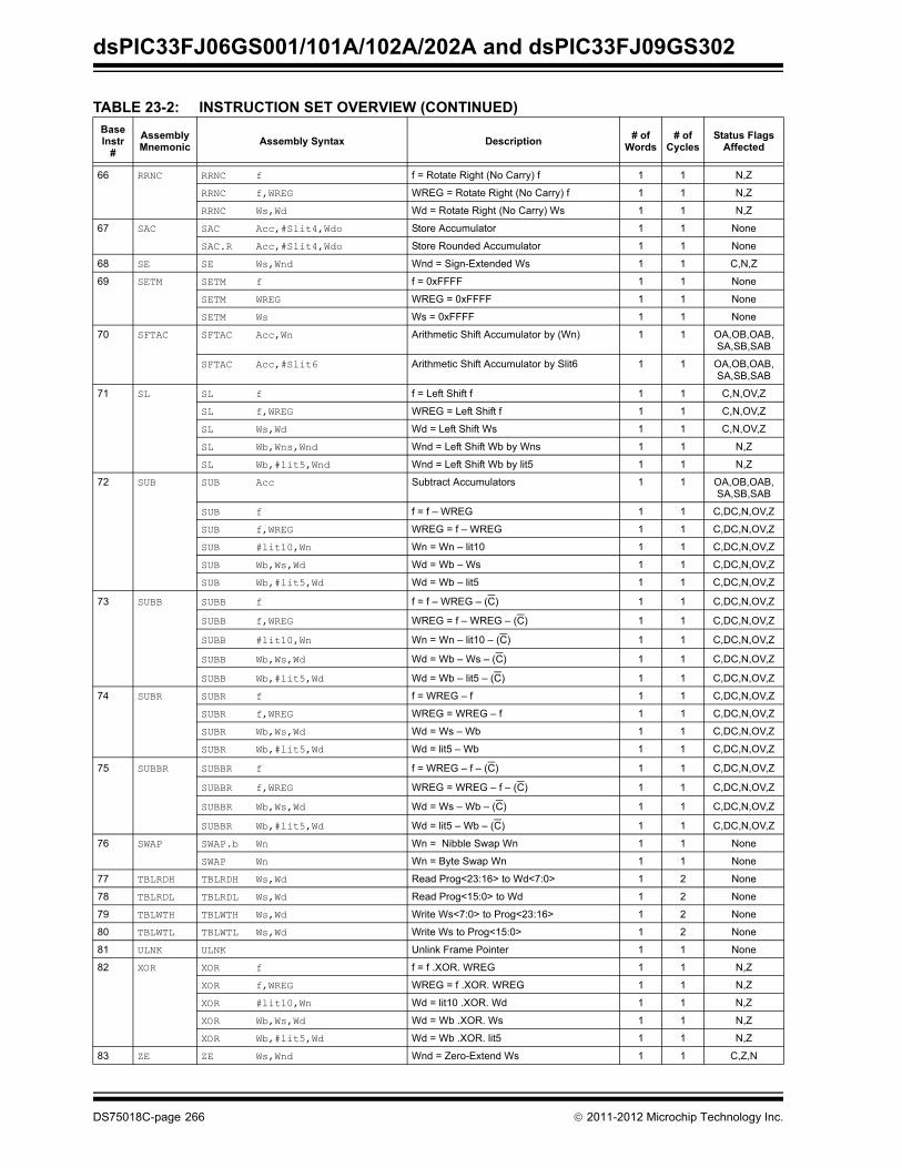
dsPIC33FJ06GS001/101A/102A/202A and dsPIC33FJ09GS302
66 RRNC RRNC f f = Rotate Right (No Carry) f 1 1 N,Z
RRNC f,WREG WREG = Rotate Right (No Carry) f 1 1 N,Z
RRNC Ws,Wd Wd = Rotate Right (No Carry) Ws 1 1 N,Z
67 SAC SAC Acc,#Slit4,Wdo Store Accumulator 1 1 None
SAC.R Acc,#Slit4,Wdo Store Rounded Accumulator 1 1 None
68 SE SE Ws,Wnd Wnd = Sign-Extended Ws 1 1 C,N,Z
69 SETM SETM f f = 0xFFFF 1 1 None
SETM WREG WREG = 0xFFFF 1 1 None
SETM Ws Ws = 0xFFFF 1 1 None
70 SFTAC SFTAC Acc,Wn Arithmetic Shift Accumulator by (Wn) 1 1 OA,OB,OAB,SA,SB,SAB
SFTAC Acc,#Slit6 Arithmetic Shift Accumulator by Slit6 1 1 OA,OB,OAB,SA,SB,SAB
71 SL SL f f = Left Shift f 1 1 C,N,OV,Z
SL f,WREG WREG = Left Shift f 1 1 C,N,OV,Z
SL Ws,Wd Wd = Left Shift Ws 1 1 C,N,OV,Z
SL Wb,Wns,Wnd Wnd = Left Shift Wb by Wns 1 1 N,Z
SL Wb,#lit5,Wnd Wnd = Left Shift Wb by lit5 1 1 N,Z
72 SUB SUB Acc Subtract Accumulators 1 1 OA,OB,OAB,SA,SB,SAB
SUB f f = f – WREG 1 1 C,DC,N,OV,Z
SUB f,WREG WREG = f – WREG 1 1 C,DC,N,OV,Z
SUB #lit10,Wn Wn = Wn – lit10 1 1 C,DC,N,OV,Z
SUB Wb,Ws,Wd Wd = Wb – Ws 1 1 C,DC,N,OV,Z
SUB Wb,#lit5,Wd Wd = Wb – lit5 1 1 C,DC,N,OV,Z
73 SUBB SUBB f f = f – WREG – (C) 1 1 C,DC,N,OV,Z
SUBB f,WREG WREG = f – WREG – (C) 1 1 C,DC,N,OV,Z
SUBB #lit10,Wn Wn = Wn – lit10 – (C) 1 1 C,DC,N,OV,Z
SUBB Wb,Ws,Wd Wd = Wb – Ws – (C) 1 1 C,DC,N,OV,Z
SUBB Wb,#lit5,Wd Wd = Wb – lit5 – (C) 1 1 C,DC,N,OV,Z
74 SUBR SUBR f f = WREG – f 1 1 C,DC,N,OV,Z
SUBR f,WREG WREG = WREG – f 1 1 C,DC,N,OV,Z
SUBR Wb,Ws,Wd Wd = Ws – Wb 1 1 C,DC,N,OV,Z
SUBR Wb,#lit5,Wd Wd = lit5 – Wb 1 1 C,DC,N,OV,Z
75 SUBBR SUBBR f f = WREG – f – (C) 1 1 C,DC,N,OV,Z
SUBBR f,WREG WREG = WREG – f – (C) 1 1 C,DC,N,OV,Z
SUBBR Wb,Ws,Wd Wd = Ws – Wb – (C) 1 1 C,DC,N,OV,Z
SUBBR Wb,#lit5,Wd Wd = lit5 – Wb – (C) 1 1 C,DC,N,OV,Z
76 SWAP SWAP.b Wn Wn = Nibble Swap Wn 1 1 None
SWAP Wn Wn = Byte Swap Wn 1 1 None
77 TBLRDH TBLRDH Ws,Wd Read Prog<23:16> to Wd<7:0> 1 2 None
78 TBLRDL TBLRDL Ws,Wd Read Prog<15:0> to Wd 1 2 None
79 TBLWTH TBLWTH Ws,Wd Write Ws<7:0> to Prog<23:16> 1 2 None
80 TBLWTL TBLWTL Ws,Wd Write Ws to Prog<15:0> 1 2 None
81 ULNK ULNK Unlink Frame Pointer 1 1 None
82 XOR XOR f f = f .XOR. WREG 1 1 N,Z
XOR f,WREG WREG = f .XOR. WREG 1 1 N,Z
XOR #lit10,Wn Wd = lit10 .XOR. Wd 1 1 N,Z
XOR Wb,Ws,Wd Wd = Wb .XOR. Ws 1 1 N,Z
XOR Wb,#lit5,Wd Wd = Wb .XOR. lit5 1 1 N,Z
83 ZE ZE Ws,Wnd Wnd = Zero-Extend Ws 1 1 C,Z,N
TABLE 23-2: INSTRUCTION SET OVERVIEW (CONTINUED)
BaseInstr
#
AssemblyMnemonic
Assembly Syntax Description# of
Words# of
CyclesStatus Flags
Affected
DS75018C-page 266 2011-2012 Microchip Technology Inc.

dsPIC33FJ06GS001/101A/102A/202A and dsPIC33FJ09GS302
24.0 DEVELOPMENT SUPPORT
The PIC® microcontrollers and dsPIC® digital signalcontrollers are supported with a full range of softwareand hardware development tools:
• Integrated Development Environment
- MPLAB® IDE Software
• Compilers/Assemblers/Linkers
- MPLAB C Compiler for Various DeviceFamilies
- HI-TECH C® for Various Device Families
- MPASMTM Assembler
- MPLINKTM Object Linker/MPLIBTM Object Librarian
- MPLAB Assembler/Linker/Librarian forVarious Device Families
• Simulators
- MPLAB SIM Software Simulator
• Emulators
- MPLAB REAL ICE™ In-Circuit Emulator
• In-Circuit Debuggers
- MPLAB ICD 3
- PICkit™ 3 Debug Express
• Device Programmers
- PICkit™ 2 Programmer
- MPLAB PM3 Device Programmer
• Low-Cost Demonstration/Development Boards, Evaluation Kits, and Starter Kits
24.1 MPLAB Integrated Development Environment Software
The MPLAB IDE software brings an ease of softwaredevelopment previously unseen in the 8/16/32-bitmicrocontroller market. The MPLAB IDE is a Windows®
operating system-based application that contains:
• A single graphical interface to all debugging tools
- Simulator
- Programmer (sold separately)
- In-Circuit Emulator (sold separately)
- In-Circuit Debugger (sold separately)
• A full-featured editor with color-coded context
• A multiple project manager
• Customizable data windows with direct edit of contents
• High-level source code debugging
• Mouse over variable inspection
• Drag and drop variables from source to watch windows
• Extensive on-line help
• Integration of select third party tools, such as IAR C Compilers
The MPLAB IDE allows you to:
• Edit your source files (either C or assembly)
• One-touch compile or assemble, and download to emulator and simulator tools (automatically updates all project information)
• Debug using:
- Source files (C or assembly)
- Mixed C and assembly
- Machine code
MPLAB IDE supports multiple debugging tools in asingle development paradigm, from the cost-effectivesimulators, through low-cost in-circuit debuggers, tofull-featured emulators. This eliminates the learningcurve when upgrading to tools with increased flexibilityand power.
2011-2012 Microchip Technology Inc. DS75018C-page 267

dsPIC33FJ06GS001/101A/102A/202A and dsPIC33FJ09GS302
24.2 MPLAB C Compilers for Various Device Families
The MPLAB C Compiler code development systemsare complete ANSI C compilers for Microchip’s PIC18,PIC24 and PIC32 families of microcontrollers and thedsPIC30 and dsPIC33 families of digital signal control-lers. These compilers provide powerful integrationcapabilities, superior code optimization and ease ofuse.
For easy source level debugging, the compilers providesymbol information that is optimized to the MPLAB IDEdebugger.
24.3 HI-TECH C for Various Device Families
The HI-TECH C Compiler code development systemsare complete ANSI C compilers for Microchip’s PICfamily of microcontrollers and the dsPIC family of digitalsignal controllers. These compilers provide powerfulintegration capabilities, omniscient code generationand ease of use.
For easy source level debugging, the compilers providesymbol information that is optimized to the MPLAB IDEdebugger.
The compilers include a macro assembler, linker, pre-processor, and one-step driver, and can run on multipleplatforms.
24.4 MPASM Assembler
The MPASM Assembler is a full-featured, universalmacro assembler for PIC10/12/16/18 MCUs.
The MPASM Assembler generates relocatable objectfiles for the MPLINK Object Linker, Intel® standard HEXfiles, MAP files to detail memory usage and symbolreference, absolute LST files that contain source linesand generated machine code and COFF files fordebugging.
The MPASM Assembler features include:
• Integration into MPLAB IDE projects
• User-defined macros to streamline assembly code
• Conditional assembly for multipurpose source files
• Directives that allow complete control over the assembly process
24.5 MPLINK Object Linker/MPLIB Object Librarian
The MPLINK Object Linker combines relocatableobjects created by the MPASM Assembler and theMPLAB C18 C Compiler. It can link relocatable objectsfrom precompiled libraries, using directives from alinker script.
The MPLIB Object Librarian manages the creation andmodification of library files of precompiled code. Whena routine from a library is called from a source file, onlythe modules that contain that routine will be linked inwith the application. This allows large libraries to beused efficiently in many different applications.
The object linker/library features include:
• Efficient linking of single libraries instead of many smaller files
• Enhanced code maintainability by grouping related modules together
• Flexible creation of libraries with easy module listing, replacement, deletion and extraction
24.6 MPLAB Assembler, Linker and Librarian for Various Device Families
MPLAB Assembler produces relocatable machinecode from symbolic assembly language for PIC24,PIC32 and dsPIC devices. MPLAB C Compiler usesthe assembler to produce its object file. The assemblergenerates relocatable object files that can then bearchived or linked with other relocatable object files andarchives to create an executable file. Notable featuresof the assembler include:
• Support for the entire device instruction set
• Support for fixed-point and floating-point data
• Command line interface
• Rich directive set
• Flexible macro language
• MPLAB IDE compatibility
DS75018C-page 268 2011-2012 Microchip Technology Inc.

dsPIC33FJ06GS001/101A/102A/202A and dsPIC33FJ09GS302
24.7 MPLAB SIM Software Simulator
The MPLAB SIM Software Simulator allows codedevelopment in a PC-hosted environment by simulat-ing the PIC MCUs and dsPIC® DSCs on an instructionlevel. On any given instruction, the data areas can beexamined or modified and stimuli can be applied froma comprehensive stimulus controller. Registers can belogged to files for further run-time analysis. The tracebuffer and logic analyzer display extend the power ofthe simulator to record and track program execution,actions on I/O, most peripherals and internal registers.
The MPLAB SIM Software Simulator fully supportssymbolic debugging using the MPLAB C Compilers,and the MPASM and MPLAB Assemblers. The soft-ware simulator offers the flexibility to develop anddebug code outside of the hardware laboratory envi-ronment, making it an excellent, economical softwaredevelopment tool.
24.8 MPLAB REAL ICE In-Circuit Emulator System
MPLAB REAL ICE In-Circuit Emulator System isMicrochip’s next generation high-speed emulator forMicrochip Flash DSC and MCU devices. It debugs andprograms PIC® Flash MCUs and dsPIC® Flash DSCswith the easy-to-use, powerful graphical user interface ofthe MPLAB Integrated Development Environment (IDE),included with each kit.
The emulator is connected to the design engineer’s PCusing a high-speed USB 2.0 interface and is connectedto the target with either a connector compatible with in-circuit debugger systems (RJ11) or with the new high-speed, noise tolerant, Low-Voltage Differential Signal(LVDS) interconnection (CAT5).
The emulator is field upgradable through future firmwaredownloads in MPLAB IDE. In upcoming releases ofMPLAB IDE, new devices will be supported, and newfeatures will be added. MPLAB REAL ICE offerssignificant advantages over competitive emulatorsincluding low-cost, full-speed emulation, run-timevariable watches, trace analysis, complex breakpoints, aruggedized probe interface and long (up to three meters)interconnection cables.
24.9 MPLAB ICD 3 In-Circuit Debugger System
MPLAB ICD 3 In-Circuit Debugger System is Micro-chip’s most cost effective high-speed hardwaredebugger/programmer for Microchip Flash Digital Sig-nal Controller (DSC) and microcontroller (MCU)devices. It debugs and programs PIC® Flash microcon-trollers and dsPIC® DSCs with the powerful, yet easy-to-use graphical user interface of MPLAB IntegratedDevelopment Environment (IDE).
The MPLAB ICD 3 In-Circuit Debugger probe is con-nected to the design engineer’s PC using a high-speedUSB 2.0 interface and is connected to the target with aconnector compatible with the MPLAB ICD 2 or MPLABREAL ICE systems (RJ-11). MPLAB ICD 3 supports allMPLAB ICD 2 headers.
24.10 PICkit 3 In-Circuit Debugger/Programmer and PICkit 3 Debug Express
The MPLAB PICkit 3 allows debugging and program-ming of PIC® and dsPIC® Flash microcontrollers at amost affordable price point using the powerful graphicaluser interface of the MPLAB Integrated DevelopmentEnvironment (IDE). The MPLAB PICkit 3 is connectedto the design engineer’s PC using a full speed USBinterface and can be connected to the target via anMicrochip debug (RJ-11) connector (compatible withMPLAB ICD 3 and MPLAB REAL ICE). The connectoruses two device I/O pins and the reset line to imple-ment in-circuit debugging and In-Circuit Serial Pro-gramming™.
The PICkit 3 Debug Express include the PICkit 3, demoboard and microcontroller, hookup cables and CDROMwith user’s guide, lessons, tutorial, compiler andMPLAB IDE software.
2011-2012 Microchip Technology Inc. DS75018C-page 269

dsPIC33FJ06GS001/101A/102A/202A and dsPIC33FJ09GS302
24.11 PICkit 2 Development Programmer/Debugger and PICkit 2 Debug Express
The PICkit™ 2 Development Programmer/Debugger isa low-cost development tool with an easy to use inter-face for programming and debugging Microchip’s Flashfamilies of microcontrollers. The full featuredWindows® programming interface supports baseline(PIC10F, PIC12F5xx, PIC16F5xx), midrange(PIC12F6xx, PIC16F), PIC18F, PIC24, dsPIC30,dsPIC33, and PIC32 families of 8-bit, 16-bit, and 32-bitmicrocontrollers, and many Microchip Serial EEPROMproducts. With Microchip’s powerful MPLAB IntegratedDevelopment Environment (IDE) the PICkit™ 2enables in-circuit debugging on most PIC® microcon-trollers. In-Circuit-Debugging runs, halts and singlesteps the program while the PIC microcontroller isembedded in the application. When halted at a break-point, the file registers can be examined and modified.
The PICkit 2 Debug Express include the PICkit 2, demoboard and microcontroller, hookup cables and CDROMwith user’s guide, lessons, tutorial, compiler andMPLAB IDE software.
24.12 MPLAB PM3 Device Programmer
The MPLAB PM3 Device Programmer is a universal,CE compliant device programmer with programmablevoltage verification at VDDMIN and VDDMAX formaximum reliability. It features a large LCD display(128 x 64) for menus and error messages and a modu-lar, detachable socket assembly to support variouspackage types. The ICSP™ cable assembly is includedas a standard item. In Stand-Alone mode, the MPLABPM3 Device Programmer can read, verify and programPIC devices without a PC connection. It can also setcode protection in this mode. The MPLAB PM3connects to the host PC via an RS-232 or USB cable.The MPLAB PM3 has high-speed communications andoptimized algorithms for quick programming of largememory devices and incorporates an MMC card for filestorage and data applications.
24.13 Demonstration/Development Boards, Evaluation Kits, and Starter Kits
A wide variety of demonstration, development andevaluation boards for various PIC MCUs and dsPICDSCs allows quick application development on fully func-tional systems. Most boards include prototyping areas foradding custom circuitry and provide application firmwareand source code for examination and modification.
The boards support a variety of features, including LEDs,temperature sensors, switches, speakers, RS-232interfaces, LCD displays, potentiometers and additionalEEPROM memory.
The demonstration and development boards can beused in teaching environments, for prototyping customcircuits and for learning about various microcontrollerapplications.
In addition to the PICDEM™ and dsPICDEM™ demon-stration/development board series of circuits, Microchiphas a line of evaluation kits and demonstration softwarefor analog filter design, KEELOQ® security ICs, CAN,IrDA®, PowerSmart battery management, SEEVAL®
evaluation system, Sigma-Delta ADC, flow ratesensing, plus many more.
Also available are starter kits that contain everythingneeded to experience the specified device. This usuallyincludes a single application and debug capability, allon one board.
Check the Microchip web page (www.microchip.com)for the complete list of demonstration, developmentand evaluation kits.
DS75018C-page 270 2011-2012 Microchip Technology Inc.

dsPIC33FJ06GS001/101A/102A/202A and dsPIC33FJ09GS302
25.0 ELECTRICAL CHARACTERISTICS
This section provides an overview of dsPIC33FJ06GS001/101A/102A/202A and dsPIC33FJ09GS302 electricalcharacteristics. Additional information will be provided in future revisions of this document as it becomes available.
Absolute maximum ratings are listed below. Exposure to these maximum rating conditions for extended periods mayaffect device reliability. Functional operation of the device at these or any other conditions above the parametersindicated in the operation listings of this specification is not implied.
Absolute Maximum Ratings(1)
Ambient temperature under bias............................................................................................................ .-40°C to +125°C
Storage temperature .............................................................................................................................. -65°C to +150°C
Voltage on VDD with respect to VSS .......................................................................................................... -0.3V to +4.0V
Voltage on any pin that is not 5V tolerant, with respect to VSS(3).................................................... -0.3V to (VDD + 0.3V)
Voltage on any 5V tolerant pin with respect to VSS, when VDD 3.0V(3).................................................. -0.3V to +5.6V
Voltage on any 5V tolerant pin with respect to Vss, when VDD < 3.0V(3)........................................ -0.3V to (VDD + 0.3V)
Maximum current out of VSS pin ...........................................................................................................................300 mA
Maximum current into VDD pin(2)...........................................................................................................................250 mA
Maximum current sourced/sunk by any 4x I/O pin ..................................................................................................15 mA
Maximum current sourced/sunk by any 16x I/O pin ................................................................................................45 mA
Maximum current sunk by all ports .......................................................................................................................200 mA
Maximum current sourced by all ports(2)...............................................................................................................200 mA
Note 1: Stresses above those listed under “Absolute Maximum Ratings” may cause permanent damage to thedevice. This is a stress rating only, and functional operation of the device at those or any other conditionsabove those indicated in the operation listings of this specification is not implied. Exposure to maximumrating conditions for extended periods may affect device reliability.
2: Maximum allowable current is a function of device maximum power dissipation (see Table 25-2).
3: See the “Pin Diagrams” section for 5V tolerant pins.
2011-2012 Microchip Technology Inc. DS75018C-page 271

dsPIC33FJ06GS001/101A/102A/202A and dsPIC33FJ09GS302
25.1 DC Characteristics TABLE 25-1: OPERATING MIPS vs. VOLTAGE
CharacteristicVDD Range(in Volts)
Temp Range(in °C)
Maximum MIPS
dsPIC33FJ06GS001/101A/102A/202A and dsPIC33FJ09GS302
— VBOR-3.6V(1) -40°C to +85°C 40
— VBOR-3.6V(1) -40°C to +125°C 40
Note 1: Overall functional device operation at VBORMIN < VDD < VDDMIN is tested but not characterized. All device analog modules, such as the ADC, etc., will function but with degraded performance below VDDMIN. Refer to Parameter BO10 in Table 25-11 for BOR values.
TABLE 25-2: THERMAL OPERATING CONDITIONS
Rating Symbol Min. Typ. Max. Unit
Industrial Temperature Devices
Operating Junction Temperature Range TJ -40 — +125 °C
Operating Ambient Temperature Range TA -40 — +85 °C
Extended Temperature Devices
Operating Junction Temperature Range TJ -40 — +140 °C
Operating Ambient Temperature Range TA -40 — +125 °C
Power DissipationInternal Chip Power Dissipation:
PINT = VDD x (IDD – IOH) PD PINT + PI/O WI/O Pin Power Dissipation:
I/O = ({VDD – VOH} x IOH) + (VOL x IOL)
Maximum Allowed Power Dissipation PDMAX (TJ – TA)/JA W
TABLE 25-3: THERMAL PACKAGING CHARACTERISTICS
Characteristic Symbol Typ. Max. Unit Notes
Package Thermal Resistance, 18-Pin SOIC JA 57 — °C/W 1
Package Thermal Resistance, 18-pin PDIP JA 66 — °C/W 1
Package Thermal Resistance, 20-pin SSOP JA 64 — °C/W 1
Package Thermal Resistance, 28-Pin QFN-S JA 34 — °C/W 1
Package Thermal Resistance, 28-pin SSOP JA 71 — °C/W 1
Package Thermal Resistance, 28-Pin SOIC JA 47 — °C/W 1
Package Thermal Resistance, 28-Pin SPDIP JA 45 — °C/W 1
Package Thermal Resistance, 36-Pin VTLA JA 29 — °C/W 1
Note 1: Junction to ambient thermal resistance, Theta-JA (JA) numbers are achieved by package simulations.
DS75018C-page 272 2011-2012 Microchip Technology Inc.

dsPIC33FJ06GS001/101A/102A/202A and dsPIC33FJ09GS302
TABLE 25-4: DC TEMPERATURE AND VOLTAGE SPECIFICATIONS
DC CHARACTERISTICSStandard Operating Conditions: 3.0V to 3.6V (unless otherwise stated)Operating temperature -40°C TA +85°C for Industrial
-40°C TA +125°C for Extended
Param. Symbol Characteristic Min. Typ.(1) Max. Units Conditions
Operating Voltage
DC10 VDD Supply Voltage(4) VBOR — 3.6 V Industrial and Extended
DC12 VDR RAM Data Retention Voltage(2)
1.8 — — V
DC16 VPOR VDD Start Voltageto Ensure Internal Power-on Reset Signal
— — VSS V
DC17 SVDD VDD Rise Rate(3)
to Ensure InternalPower-on Reset Signal
0.03 — — V/ms 0-3.0V in 0.1s
Note 1: Data in “Typ” column is at 3.3V, +25°C unless otherwise stated.
2: This is the limit to which VDD may be lowered without losing RAM data.
3: These parameters are characterized but not tested in manufacturing.
4: Overall functional device operation at VBORMIN < VDD < VDDMIN is tested but not characterized. All device analog modules, such as the ADC, etc., will function but with degraded performance below VDDMIN. Refer to Parameter BO10 in Table 25-11 for BOR values.
2011-2012 Microchip Technology Inc. DS75018C-page 273

dsPIC33FJ06GS001/101A/102A/202A and dsPIC33FJ09GS302
TABLE 25-5: DC CHARACTERISTICS: OPERATING CURRENT (IDD)
DC CHARACTERISTICSStandard Operating Conditions: 3.0V to 3.6V (unless otherwise stated)Operating temperature -40°C TA +85°C for Industrial
-40°C TA +125°C for Extended
Param. Typical(1) Max. Units Conditions
Operating Current (IDD)(2)
DC20d 15 23 mA -40°C
3.3V 10 MIPSDC20a 15 23 mA +25°C
DC20b 15 23 mA +85°C
DC20c 15 23 mA +125°C
DC21d 23 34 mA -40°C
3.3V 16 MIPS(3)DC21a 23 34 mA +25°C
DC21b 23 34 mA +85°C
DC21c 23 34 mA +125°C
DC22d 25 38 mA -40°C
3.3V 20 MIPS(3)DC22a 25 38 mA +25°C
DC22b 25 38 mA +85°C
DC22c 25 38 mA +125°C
DC23d 34 51 mA -40°C
3.3V 30 MIPS(3)DC23a 34 51 mA +25°C
DC23b 34 51 mA +85°C
DC23c 34 51 mA +125°C
DC24d 43 64 mA -40°C
3.3V 40 MIPS(3)DC24a 43 64 mA +25°C
DC24b 43 64 mA +85°C
DC24c 43 64 mA +125°C
DC25d 83 125 mA -40°C
3.3V
40 MIPSSee Note 2, except PWM and ADCare operating at maximum speed
(PTCON2 = 0x0000)
DC25a 83 125 mA +25°C
DC25b 83 125 mA +85°C
DC25c 83 125 mA +125°C
Note 1: Data in “Typical” column is at 3.3V, +25°C unless otherwise stated.
2: IDD is primarily a function of the operating voltage and frequency. Other factors, such as I/O pin loading and switching rate, oscillator type, internal code execution pattern and temperature, also have an impact on the current consumption. The test conditions for all IDD measurements are as follows:
• Oscillator is configured in EC mode, OSC1 is driven with external square wave from rail-to-rail
• CLKO is configured as an I/O input pin in the Configuration Word
• All I/O pins are configured as inputs and pulled to VSS
• MCLR = VDD; WDT and FSCM are disabled
• CPU, SRAM, program memory and data memory are operational
• No peripheral modules are operating; however, every peripheral is being clocked (PMDx bits are all zeroed)
• CPU is executing while(1) statement
3: These parameters are characterized but not tested in manufacturing.
DS75018C-page 274 2011-2012 Microchip Technology Inc.

dsPIC33FJ06GS001/101A/102A/202A and dsPIC33FJ09GS302
TABLE 25-6: DC CHARACTERISTICS: IDLE CURRENT (IIDLE)
DC CHARACTERISTICSStandard Operating Conditions: 3.0V to 3.6V (unless otherwise stated)Operating temperature -40°C TA +85°C for Industrial
-40°C TA +125°C for Extended
Param. Typical(1) Max. Units Conditions
Idle Current (IIDLE): Core Off Clock On Base Current(2)
DC40d 13 21 mA -40°C
3.3V 10 MIPSDC40a 13 21 mA +25°C
DC40b 13 21 mA +85°C
DC40c 13 21 mA +125°C
DC41d 16 24 mA -40°C
3.3V 16 MIPS(3)DC41a 16 mA +25°C24
DC41b 16 24 mA +85°C
DC41c 16 24 mA +125°C
DC42d 17 27 mA -40°C
3.3V 20 MIPS(3)DC42a 17 27 mA +25°C
DC42b 17 27 mA +85°C
DC42c 17 27 mA +125°C
DC43d 20 32 mA -40°C
3.3V 30 MIPS(3)DC43a 20 32 mA +25°C
DC43b 20 32 mA +85°C
DC43c 20 32 mA +125°C
DC44d 23 37 mA -40°C
3.3V 40 MIPSDC44a 23 37 mA +25°C
DC44b 23 37 mA +85°C
DC44c 23 37 mA +125°C
Note 1: Data in “Typical” column is at 3.3V, +25°C unless otherwise stated.
2: Base Idle current is measured as follows:
• CPU core is off, oscillator is configured in EC mode, OSC1 is driven with external square wave from rail-to-rail
• CLKO is configured as an I/O input pin in the Configuration Word
• All I/O pins are configured as inputs and pulled to VSS
• MCLR = VDD; WDT and FSCM are disabled
• No peripheral modules are operating; however, every peripheral is being clocked (PMDx bits are all zeroed)
3: These parameters are characterized but not tested in manufacturing.
2011-2012 Microchip Technology Inc. DS75018C-page 275

dsPIC33FJ06GS001/101A/102A/202A and dsPIC33FJ09GS302
TABLE 25-7: DC CHARACTERISTICS: POWER-DOWN CURRENT (IPD)
DC CHARACTERISTICSStandard Operating Conditions: 3.0V to 3.6V (unless otherwise stated)Operating temperature -40°C TA +85°C for Industrial
-40°C TA +125°C for Extended
Param. Typical(1) Max. Units Conditions
Power-Down Current (IPD)(2,4)
DC60d 125 500 A -40°C
3.3V Base Power-Down CurrentDC60a 135 500 A +25°C
DC60b 235 500 A +85°C
DC60c 565 950 A +125°C
DC61d 40 50 A -40°C
3.3V Watchdog Timer Current: IWDT(3)DC61a 40 50 A +25°C
DC61b 40 50 A +85°C
DC61c 80 90 A +125°C
Note 1: Data in the Typical column is at 3.3V, +25°C unless otherwise stated.
2: IPD current is measured as follows:
• CPU core is off, oscillator is configured in EC mode, OSC1 is driven with external square wave from rail-to-rail
• CLKO is configured as an I/O input pin in the Configuration Word
• All I/O pins are configured as inputs and pulled to VSS
• MCLR = VDD, WDT and FSCM are disabled
• All peripheral modules are disabled (PMDx bits are all ‘1’s)
• VREGS bit (RCON<8>) = 1 (i.e., core regulator is set to standby while the device is in Sleep mode)
3: The current is the additional current consumed when the WDT module is enabled. This current should be added to the base IPD current.
4: These currents are measured on the device containing the most memory in this family.
DS75018C-page 276 2011-2012 Microchip Technology Inc.

dsPIC33FJ06GS001/101A/102A/202A and dsPIC33FJ09GS302
TABLE 25-8: DC CHARACTERISTICS: DOZE CURRENT (IDOZE)
DC CHARACTERISTICSStandard Operating Conditions: 3.0V to 3.6V (unless otherwise stated)Operating temperature -40°C TA +85°C for Industrial
-40°C TA +125°C for Extended
Param. Typical(1) Max. Doze Ratio Units Conditions
Doze Current (IDOZE)(2)
DC73a 30 45 1:2 mA
-40°C 3.3V 40 MIPSDC73f 16 23 1:64 mA
DC73g 16 23 1:128 mA
DC70a 30 45 1:2 mA
+25°C 3.3V 40 MIPSDC70f 16 23 1:64 mA
DC70g 16 23 1:128 mA
DC71a 30 45 1:2 mA
+85°C 3.3V 40 MIPSDC71f 16 23 1:64 mA
DC71g 16 23 1:128 mA
DC72a 30 45 1:2 mA
+125°C 3.3V 40 MIPSDC72f 16 23 1:64 mA
DC72g 16 23 1:128 mA
Note 1: Data in the Typical column is at 3.3V, +25°C unless otherwise stated.
2: IDOZE is primarily a function of the operating voltage and frequency. Other factors, such as I/O pin loading and switching rate, oscillator type, internal code execution pattern and temperature, also have an impact on the current consumption. The test conditions for all IDOZE measurements are as follows:
• Oscillator is configured in EC mode, OSC1 is driven with external square wave from rail-to-rail
• CLKO is configured as an I/O input pin in the Configuration Word
• All I/O pins are configured as inputs and pulled to VSS
• MCLR = VDD; WDT and FSCM are disabled
• CPU, SRAM, program memory and data memory are operational
• No peripheral modules are operating; however, every peripheral is being clocked (PMDx bits are all zeroed)
• CPU is executing while(1) statement
2011-2012 Microchip Technology Inc. DS75018C-page 277

dsPIC33FJ06GS001/101A/102A/202A and dsPIC33FJ09GS302
TABLE 25-9: DC CHARACTERISTICS: I/O PIN INPUT SPECIFICATIONS
DC CHARACTERISTICS
Standard Operating Conditions: 3.0V to 3.6V(unless otherwise stated)Operating temperature -40°C TA +85°C for Industrial
-40°C TA +125°C for Extended
Param. Symbol Characteristic Min. Typ.(1) Max. Units Conditions
VIL Input Low Voltage
DI10 I/O Pins VSS — 0.2 VDD V
DI15 MCLR VSS — 0.2 VDD V
DI16 I/O Pins with OSC1 VSS — 0.2 VDD V
DI18 SDA1, SCL1 VSS — 0.3 VDD V SMBus disabled
DI19 SDA1, SCL1 VSS — 0.8 V SMBus enabled
VIH Input High Voltage
DI20DI21
I/O Pins Not 5V Tolerant(4)
I/O Pins 5V Tolerant(4)0.7 VDD
0.7 VDD
——
VDD
5.5VV
DI28DI29
SDA1, SCL1SDA1, SCL1
0.7 VDD
2.1——
5.55.5
VV
SMBus disabledSMBus enabled
ICNPU CNx Pull-up Current
DI30 — 250 — A VDD = 3.3V, VPIN = VSS
IIL Input Leakage Current(2,3,4)
DI50 I/O Pins:4x Sink Driver PinsRA0-RA2, RB0-RB2, RB5-RB10, RB15
16x Sink Driver PinsRA3, RA4, RB3, RB4, RB11-RB14
—
—
—
—
±2
±8
A
A
VSS VPIN VDD,Pin at high-impedance
VSS VPIN VDD,Pin at high-impedance
DI55 MCLR — — ±2 A VSS VPIN VDD
DI56 OSC1 — — ±2 A VSS VPIN VDD, XT and HS modes
Note 1: Data in “Typ” column is at 3.3V, +25°C unless otherwise stated.
2: The leakage current on the MCLR pin is strongly dependent on the applied voltage level. The specified levels represent normal operating conditions. Higher leakage current may be measured at different input voltages.
3: Negative current is defined as current sourced by the pin.
4: See the “Pin Diagrams” section for the list of 5V tolerant I/O pins.
5: VIL source < (VSS – 0.3); characterized but not tested.
6: Non-5V tolerant pins VIH source > (VDD + 0.3), 5V tolerant pins VIH source > 5.5V; characterized but not tested.
7: Digital 5V tolerant pins cannot tolerate any “positive” input injection current from input sources > 5.5V.
8: Injection currents > | 0 | can affect the ADC results by approximately 4-6 counts.
9: Any number and/or combination of I/O pins, not excluded under IICL or IICH conditions, are permitted provided the mathematical “absolute instantaneous” sum of the input injection currents from all pins do not exceed the specified limit; characterized but not tested.
DS75018C-page 278 2011-2012 Microchip Technology Inc.

dsPIC33FJ06GS001/101A/102A/202A and dsPIC33FJ09GS302
IICL Input Low Injection Current
DI60a 0 — -5(5,8) mA All pins except VDD, VSS, AVDD, AVSS, MCLR, VCAP and RB5
IICH Input High Injection Current
DI60b 0 — +5(6,7,8) mA All pins except VDD, VSS, AVDD, AVSS, MCLR, VCAP, RB5 and digital 5V tolerant designated pins
IICT Total Input Injection Current
DI60c (sum of all I/O and control pins) -20(9) — +20(9) mA Absolute instantaneous sum of all ± input injection currents from all I/O pins( | IICL + | IICH | ) IICT
TABLE 25-9: DC CHARACTERISTICS: I/O PIN INPUT SPECIFICATIONS (CONTINUED)
DC CHARACTERISTICS
Standard Operating Conditions: 3.0V to 3.6V(unless otherwise stated)Operating temperature -40°C TA +85°C for Industrial
-40°C TA +125°C for Extended
Param. Symbol Characteristic Min. Typ.(1) Max. Units Conditions
Note 1: Data in “Typ” column is at 3.3V, +25°C unless otherwise stated.
2: The leakage current on the MCLR pin is strongly dependent on the applied voltage level. The specified levels represent normal operating conditions. Higher leakage current may be measured at different input voltages.
3: Negative current is defined as current sourced by the pin.
4: See the “Pin Diagrams” section for the list of 5V tolerant I/O pins.
5: VIL source < (VSS – 0.3); characterized but not tested.
6: Non-5V tolerant pins VIH source > (VDD + 0.3), 5V tolerant pins VIH source > 5.5V; characterized but not tested.
7: Digital 5V tolerant pins cannot tolerate any “positive” input injection current from input sources > 5.5V.
8: Injection currents > | 0 | can affect the ADC results by approximately 4-6 counts.
9: Any number and/or combination of I/O pins, not excluded under IICL or IICH conditions, are permitted provided the mathematical “absolute instantaneous” sum of the input injection currents from all pins do not exceed the specified limit; characterized but not tested.
2011-2012 Microchip Technology Inc. DS75018C-page 279

dsPIC33FJ06GS001/101A/102A/202A and dsPIC33FJ09GS302
TABLE 25-10: DC CHARACTERISTICS: I/O PIN OUTPUT SPECIFICATIONS
DC CHARACTERISTICS
Standard Operating Conditions: 3.0V to 3.6V(unless otherwise stated)Operating temperature -40°C TA +85°C for Industrial
-40°C TA +125°C for Extended
Param. Symbol Characteristic Min. Typ. Max. Units Conditions
DO10 VOL Output Low VoltageI/O Pins:4x Sink Driver Pins – RA0-RA2, RB0-RB2, RB5-RB10, RB15
— — 0.4 V IOL 6 mA, VDD = 3.3V(1)
Output Low VoltageI/O Pins:16x Sink Driver Pins – RA3, RA4, RB3, RB4, RB11-RB14
— — 0.4 V IOL 18 mA, VDD = 3.3V(1)
DO20 VOH Output High VoltageI/O Pins:4x Source Driver Pins – RA0-RA2, RB0-RB2, RB5-RB10, RB15
2.4 — — V IOH -6 mA, VDD = 3.3V(1)
Output High VoltageI/O Pins:16x Source Driver Pins – RA3, RA4, RB3, RB4, RB11-RB14
2.4 — — V IOH -18 mA, VDD = 3.3V(1)
DO20A VOH1 Output High VoltageI/O Pins:4x Source Driver Pins – RA0-RA2, RB0-RB2, RB5-RB10, RB15
1.5 — — V IOH -12 mA, VDD = 3.3V(1)
2.0 — — IOH -11 mA, VDD = 3.3V(1)
3.0 — — IOH -3 mA, VDD = 3.3V(1)
Output High VoltageI/O Pins:16x Source Driver Pins – RA3, RA4, RB3, RB4, RB11-RB14
1.5 — — V IOH -30 mA, VDD = 3.3V(1)
2.0 — — IOH -25 mA, VDD = 3.3V(1)
3.0 — — IOH -8 mA, VDD = 3.3V(1)
Note 1: These parameters are characterized, but not tested.
TABLE 25-11: ELECTRICAL CHARACTERISTICS: BOR
DC CHARACTERISTICS
Standard Operating Conditions: 3.0V to 3.6V(3)
(unless otherwise stated)Operating temperature -40°C TA +85°C for Industrial
-40°C TA +125°C for Extended
Param. Symbol Characteristic Min.(1) Typ. Max. Units Conditions
BO10 VBOR BOR Event on VDD Transition High-to-LowBOR Event is Tied to VDD Core Voltage Decrease
2.55 — 2.96 V (See Note 2)
Note 1: These parameters are for design guidance only and are not tested in manufacturing.
2: The device will operate as normal until the VDDMIN threshold is reached.
3: Overall functional device operation at VBORMIN < VDD < VDDMIN is tested but not characterized. All device analog modules, such as the ADC, etc., will function but with degraded performance below VDDMIN.
DS75018C-page 280 2011-2012 Microchip Technology Inc.

dsPIC33FJ06GS001/101A/102A/202A and dsPIC33FJ09GS302
TABLE 25-13: INTERNAL VOLTAGE REGULATOR SPECIFICATIONS
TABLE 25-12: DC CHARACTERISTICS: PROGRAM MEMORY
DC CHARACTERISTICS
Standard Operating Conditions: 3.0V to 3.6V(unless otherwise stated)Operating temperature -40°C TA +85°C for Industrial
-40°C TA +125°C for Extended
Param. Symbol Characteristic Min. Typ.(1) Max. Units Conditions
Program Flash Memory
D130 EP Cell Endurance 10,000 — — E/W -40C to +125C
D131 VPR VDD for Read VMIN — 3.6 V VMIN = Minimum operating voltage
D132B VPEW VDD for Self-Timed Write VMIN — 3.6 V VMIN = Minimum operating voltage
D134 TRETD Characteristic Retention 20 — — Year Provided no other specifications are violated, -40C to +125C
D135 IDDP Supply Current during Programming
— 10 — mA
D137a TPE Page Erase Time 20.1 — 26.5 ms TPE = 168517 FRC cycles, TA = +85°C(2)
D137b TPE Page Erase Time 19.5 — 27.3 ms TPE = 168517 FRC cycles, TA = +125°C(2)
D138a TWW Word Write Cycle Time 42.3 — 55.9 µs TWW = 355 FRC cycles, TA = +85°C(2)
D138b TWW Word Write Cycle Time 41.1 — 57.6 µs TWW = 355 FRC cycles, TA = +125°C(2)
Note 1: Data in “Typ” column is at 3.3V, +25°C unless otherwise stated.
2: Other conditions: FRC = 7.37 MHz, TUN<5:0> = ‘b011111 (for Minimum), TUN<5:0> = ‘b100000 (for Maximum). This parameter depends on the FRC accuracy (see Table 25-20) and the value of the FRC Oscillator Tuning register (see Register 9-4). For complete details on calculating the Minimum and Maximum time, see Section 5.3 “Programming Operations”.
Operating Conditions: -40°C TA +85°C for Industrial-40°C TA +125°C for Extended
Param. Symbol Characteristics Min. Typ. Max. Units Comments
CEFC External Filter Capacitor Value(1)
4.7 10 — F Capacitor must be low series resistance (< 0.5 Ohms)
Note 1: Typical VCAP voltage = 2.5 volts when VDD VDDMIN.
2011-2012 Microchip Technology Inc. DS75018C-page 281

dsPIC33FJ06GS001/101A/102A/202A and dsPIC33FJ09GS302
25.2 AC Characteristics and Timing Parameters
This section defines dsPIC33FJ06GS001/101A/102A/202A and dsPIC33FJ09GS302 AC characteristics and timingparameters.
TABLE 25-14: TEMPERATURE AND VOLTAGE SPECIFICATIONS – AC
FIGURE 25-1: LOAD CONDITIONS FOR DEVICE TIMING SPECIFICATIONS
TABLE 25-15: CAPACITIVE LOADING REQUIREMENTS ON OUTPUT PINS
AC CHARACTERISTICS
Standard Operating Conditions: 3.0V to 3.6V(unless otherwise stated)Operating temperature -40°C TA +85°C for Industrial
-40°C TA +125°C for ExtendedOperating voltage VDD range as described in Table 25-1.
Param. Symbol Characteristic Min. Typ. Max. Units Conditions
DO50 COSCO OSC2 Pin — — 15 pF In XT and HS modes when external clock is used to drive OSC1
DO56 CIO All I/O Pins and OSC2 — — 50 pF EC mode
DO58 CB SCL1, SDA1 — — 400 pF In I2C™ mode
VDD/2
CL
RL
Pin
Pin
VSS
VSS
CL
RL = 464CL = 50 pF for all pins except OSC2
15 pF for OSC2 output
Load Condition 1 – for all pins except OSC2 Load Condition 2 – for OSC2
DS75018C-page 282 2011-2012 Microchip Technology Inc.

dsPIC33FJ06GS001/101A/102A/202A and dsPIC33FJ09GS302
FIGURE 25-2: EXTERNAL CLOCK TIMING
Q1 Q2 Q3 Q4
OSC1
CLKO
Q1 Q2 Q3 Q4
OS20
OS25OS30 OS30
OS40OS41
OS31 OS31
TABLE 25-16: EXTERNAL CLOCK TIMING REQUIREMENTS
AC CHARACTERISTICS
Standard Operating Conditions: 3.0V to 3.6V(unless otherwise stated)Operating temperature -40°C TA +85°C for Industrial
-40°C TA +125°C for Extended
Param. Symbol Characteristic Min. Typ.(1) Max. Units Conditions
OS10 FIN External CLKI Frequency(External clocks allowed onlyin EC and ECPLL modes)
DC — 40 MHz EC
Oscillator Crystal Frequency 3.010
——
1032
MHzMHz
XTHS
OS20 TOSC TOSC = 1/FOSC 12.5 — DC ns
OS25 TCY Instruction Cycle Time(2) 25 — DC ns
OS30 TosL,TosH
External Clock in (OSC1)High or Low Time
0.375 x TOSC — 0.625 x TOSC ns EC
OS31 TosR,TosF
External Clock in (OSC1)Rise or Fall Time
— — 20 ns EC
OS40 TckR CLKO Rise Time(3) — 5.2 — ns
OS41 TckF CLKO Fall Time(3) — 5.2 — ns
OS42 GM External Oscillator Transconductance(4)
14 16 18 mA/V VDD = 3.3VTA = +25ºC
Note 1: Data in “Typ” column is at 3.3V, +25°C unless otherwise stated.
2: Instruction cycle period (TCY) equals two times the input oscillator time base period. All specified values are based on characterization data for that particular oscillator type, under standard operating conditions, with the device executing code. Exceeding these specified limits may result in an unstable oscillator operation and/or higher than expected current consumption. All devices are tested to operate at “min.” values with an external clock applied to the OSC1/CLKI pin. When an external clock input is used, the “max.” cycle time limit is “DC” (no clock) for all devices.
3: Measurements are taken in EC mode. The CLKO signal is measured on the OSC2 pin.
4: Data for this parameter is Preliminary. This parameter is characterized, but not tested in manufacturing.
2011-2012 Microchip Technology Inc. DS75018C-page 283

dsPIC33FJ06GS001/101A/102A/202A and dsPIC33FJ09GS302
TABLE 25-17: PLL CLOCK TIMING SPECIFICATIONS (VDD = 3.0V TO 3.6V)
AC CHARACTERISTICS
Standard Operating Conditions: 3.0V to 3.6V (unless otherwise stated)Operating temperature -40°C TA +85°C for Industrial
-40°C TA +125°C for Extended
Param. Symbol Characteristic Min. Typ.(1) Max. Units Conditions
OS50 FPLLI PLL Voltage Controlled Oscillator (VCO) Input Frequency Range
0.8 — 8 MHz ECPLL, XTPLL modes
OS51 FSYS On-Chip VCO System Frequency
100 — 200 MHz
OS52 TLOCK PLL Start-up Time (Lock Time) 0.9 1.5 3.1 mS
OS53 DCLK CLKO Stability (Jitter)(2) -3 0.5 3 % Measured over 100 ms period
Note 1: Data in “Typ” column is at 3.3V, +25°C unless otherwise stated. Parameters are for design guidance only and are not tested in manufacturing.
2: These parameters are characterized by similarity, but are not tested in manufacturing. This specification is based on clock cycle by clock cycle measurements. To calculate the effective jitter for individual time bases or communication clocks use this formula:
TABLE 25-18: AUXILIARY PLL CLOCK TIMING SPECIFICATIONS (VDD = 3.0V TO 3.6V)
AC CHARACTERISTICS
Standard Operating Conditions: 3.0V to 3.6V (unless otherwise stated)Operating temperature -40°C TA +85°C for Industrial
-40°C TA +125°C for Extended
Param. Symbol Characteristic Min. Typ.(1) Max. Units Conditions
OS56 FHPOUT On-Chip 16x PLL CCO Frequency
112 118 120 MHz
OS57 FHPIN On-Chip 16x PLL Phase Detector Input Frequency
7.0 7.37 7.5 MHz
OS58 TSU Frequency Generator Lock Time
— — 10 µs
Note 1: Data in “Typ” column is at 3.3V, +25°C unless otherwise stated. Parameters are for design guidance only and are not tested in manufacturing.
Peripheral Clock Jitter DCLK
FOSC
Peripheral Bit Rate Clock--------------------------------------------------------------
------------------------------------------------------------------------=
For example: FOSC = 32 MHz, DCLK = 3%, SPI bit rate clock (i.e., SCK) is 2 MHz.
SPI SCK JitterDCLK
32 MHz2 MHz
--------------------
------------------------------ 3%
16---------- 3%
4-------- 0.75%= = = =
DS75018C-page 284 2011-2012 Microchip Technology Inc.

dsPIC33FJ06GS001/101A/102A/202A and dsPIC33FJ09GS302
TABLE 25-19: AC CHARACTERISTICS: INTERNAL FRC ACCURACY
AC CHARACTERISTICSStandard Operating Conditions: 3.0V to 3.6V (unless otherwise stated)Operating temperature -40°C TA +85°C for industrial
-40°C TA +125°C for Extended
Param. Characteristic Min. Typ. Max. Units Conditions
Internal FRC Accuracy @ FRC Frequency = 7.37 MHz(1)
F20a FRC -2 — +2 % -40°C TA +85°C VDD = 3.0-3.6V
F20b FRC -5 — +5 % -40°C TA +125°C VDD = 3.0-3.6V
Note 1: Frequency is calibrated at +25°C and 3.3V. TUNx bits can be used to compensate for temperature drift.
TABLE 25-20: INTERNAL LPRC ACCURACY
AC CHARACTERISTICSStandard Operating Conditions: 3.0V to 3.6V (unless otherwise stated)Operating temperature -40°C TA +85°C for Industrial
-40°C TA +125°C for Extended
Param. Characteristic Min. Typ. Max. Units Conditions
LPRC @ 32.768 kHz(1)
F21a LPRC -20 — +20 % -40°C TA +85°C VDD = 3.0-3.6V
F21b LPRC -70 — +70 % -40°C TA +125°C VDD = 3.0-3.6V
Note 1: The change of LPRC frequency as VDD changes.
2011-2012 Microchip Technology Inc. DS75018C-page 285

dsPIC33FJ06GS001/101A/102A/202A and dsPIC33FJ09GS302
FIGURE 25-3: I/O TIMING CHARACTERISTICS
Note: Refer to Figure 25-1 for load conditions.
I/O Pin(Input)
I/O Pin(Output)
DI35
Old Value New Value
DI40
DO31DO32
TABLE 25-21: I/O TIMING REQUIREMENTS
AC CHARACTERISTICS
Standard Operating Conditions: 3.0V to 3.6V(unless otherwise stated)Operating temperature -40°C TA +85°C for Industrial
-40°C TA +125°C for Extended
Param. Symbol Characteristic Min. Typ.(1) Max. Units Conditions
DO31 TIOR I/O Pins: 4x Sink Driver PinsRA0-RA2, RB0-RB2, RB5-RB10, RB15
I/O Pins: 16x Sink Driver PinsRA3, RA4, RB3, RB4, RB11-RB14
—
—
10
6
25
15
ns
ns
Refer to Figure 25-1 for test conditions
DO32 TIOF I/O Pins: 4x Sink Driver PinsRA0-RA2, RB0-RB2, RB5-RB10, RB15
I/O Pins: 16x Sink Driver PinsRA3, RA4, RB3, RB4, RB11-RB14
—
—
10
6
25
15
ns
ns
Refer to Figure 25-1 for test conditions
DI35 TINP INTx Pin High or Low Time (input) 20 — — ns
DI40 TRBP CNx High or Low Time (input) 2 — — TCY
Note 1: Data in “Typ” column is at 3.3V, +25°C unless otherwise stated.
DS75018C-page 286 2011-2012 Microchip Technology Inc.

dsPIC33FJ06GS001/101A/102A/202A and dsPIC33FJ09GS302
FIGURE 25-4: RESET, WATCHDOG TIMER, OSCILLATOR START-UP TIMER AND POWER-UP TIMER TIMING CHARACTERISTICS
VDD
MCLR
InternalPOR
PWRTTime-out
OSCTime-out
InternalReset
WatchdogTimerReset
SY11
SY10
SY20SY13
I/O Pins
SY13
Note: Refer to Figure 25-1 for load conditions.
FSCM Delay
SY35
SY30
SY12
TABLE 25-22: RESET, WATCHDOG TIMER, OSCILLATOR START-UP TIMER, POWER-UP TIMER TIMING REQUIREMENTS
AC CHARACTERISTICS
Standard Operating Conditions: 3.0V to 3.6V(unless otherwise stated)Operating temperature -40°C TA +85°C for Industrial
-40°C TA +125°C for Extended
Param. Symbol Characteristic(1) Min. Typ.(2) Max. Units Conditions
SY10 TMCL MCLR Pulse Width (low) 2 — — s -40°C to +125°C
SY11 TPWRT Power-up Timer Period — 64 — ms -40°C to +125°C
SY12 TPOR Power-on Reset Delay 3 10 30 s -40°C to +125°C
SY13 TIOZ I/O High-Impedance from MCLR Low or Watchdog Timer Reset
0.68 0.72 1.2 s
SY30 TOST Oscillator Start-up Time — 1024 TOSC — — TOSC = OSC1 period
Note 1: These parameters are characterized but not tested in manufacturing. 2: Data in “Typ” column is at 3.3V, +25°C unless otherwise stated.
2011-2012 Microchip Technology Inc. DS75018C-page 287

dsPIC33FJ06GS001/101A/102A/202A and dsPIC33FJ09GS302
FIGURE 25-5: TIMER1 AND TIMER2 EXTERNAL CLOCK TIMING CHARACTERISTICS
TABLE 25-23: TIMER1 EXTERNAL CLOCK TIMING REQUIREMENTS(1)
AC CHARACTERISTICS
Standard Operating Conditions: 3.0V to 3.6V(unless otherwise stated)Operating temperature -40°C TA +85°C for Industrial
-40°C TA +125°C for Extended
Param. Symbol Characteristic Min. Typ. Max. Units Conditions
TA10 TTXH TxCK High Time
Synchronous,no prescaler
TCY + 20 — — ns Must also meet Parameter TA15,N = prescale value(1, 8, 64, 256)
Synchronous,with prescaler
(TCY + 20)/N — — ns
Asynchronous 20 — — ns
TA11 TTXL TxCK Low Time
Synchronous,no prescaler
TCY + 20 — — ns Must also meet Parameter TA15,N = prescale value(1, 8, 64, 256)
Synchronous,with prescaler
(TCY + 20)/N — — ns
Asynchronous 20 — — ns
TA15 TTXP TxCK Input Period
Synchronous,no prescaler
2 TCY + 40 — — ns
Synchronous,with prescaler
Greater of:40 ns or
(2 TCY + 40)/N
— — — N = prescale value(1, 8, 64, 256)
Asynchronous 40 — — ns
OS60 Ft1 T1CK Oscillator Input Frequency Range (oscillator enabled by setting bit, TCS (T1CON<1>))
DC — 50 kHz
TA20 TCKEXTMRL Delay from External TxCK Clock Edge to Timer Increment
0.75 TCY + 40 — 1.75 TCY + 40 —
Note 1: Timer1 is a Type A.
Note: Refer to Figure 25-1 for load conditions.
Tx11
Tx15
Tx10
Tx20
TMRx
OS60
TxCK
DS75018C-page 288 2011-2012 Microchip Technology Inc.

dsPIC33FJ06GS001/101A/102A/202A and dsPIC33FJ09GS302
TABLE 25-24: TIMER2 EXTERNAL CLOCK TIMING REQUIREMENTS
AC CHARACTERISTICS
Standard Operating Conditions: 3.0V to 3.6V(unless otherwise stated)Operating temperature -40°C TA +85°C for Industrial
-40°C TA +125°C for Extended
Param. Symbol Characteristic Min. Typ. Max. Units Conditions
TB10 TTXH TxCK High Time Synchronous Greater of:20 ns or
(TCY + 20)/N
— — ns Must also meet Parameter TB15N = prescale value (1, 8, 64, 256)
TB11 TTXL TxCK Low Time Synchronous Greater of:20 ns or
(TCY + 20)/N
— — ns Must also meet Parameter TB15N = prescale value (1, 8, 64, 256)
TB15 TTXP TxCK Input Period Synchronous,no prescaler
TCY + 40 — — ns N = prescale value (1, 8, 64, 256)
Synchronous,with prescaler
Greater of:20 ns or
(TCY + 40)/N
TB20 TCKEXTMRL Delay from External TxCK Clock Edge to Timer Increment
0.5 TCY — 1.5 TCY —
2011-2012 Microchip Technology Inc. DS75018C-page 289

dsPIC33FJ06GS001/101A/102A/202A and dsPIC33FJ09GS302
FIGURE 25-6: INPUT CAPTURE (CAP1) TIMING CHARACTERISTICS
FIGURE 25-7: OUTPUT COMPARE MODULE (OC1) TIMING CHARACTERISTICS
TABLE 25-25: INPUT CAPTURE TIMING REQUIREMENTS
AC CHARACTERISTICS
Standard Operating Conditions: 3.0V to 3.6V(unless otherwise stated)Operating temperature -40°C TA +85°C for Industrial
-40°C TA +125°C for Extended
Param. Symbol Characteristic(1) Min. Max. Units Conditions
IC10 TccL IC1 Input Low Time No prescaler 0.5 TCY + 20 — ns
With prescaler 10 — ns
IC11 TccH IC1 Input High Time No prescaler 0.5 TCY + 20 — ns
With prescaler 10 — ns
IC15 TccP IC1 Input Period (TCY + 40)/N — ns N = prescale value (1, 4, 16)
Note 1: These parameters are characterized but not tested in manufacturing.
TABLE 25-26: OUTPUT COMPARE MODULE TIMING REQUIREMENTS
AC CHARACTERISTICS
Standard Operating Conditions: 3.0V to 3.6V(unless otherwise stated)Operating temperature -40°C TA +85°C for Industrial
-40°C TA +125°C for Extended
Param. Symbol Characteristic(1) Min. Typ. Max. Units Conditions
OC10 TccF OC1 Output Fall Time — — — ns See Parameter DO32
OC11 TccR OC1 Output Rise Time — — — ns See Parameter DO31
Note 1: These parameters are characterized but not tested in manufacturing.
IC1
IC10 IC11
IC15
Note: Refer to Figure 25-1 for load conditions.
OC1
OC11 OC10(Output Compare
Note: Refer to Figure 25-1 for load conditions.
or PWM Mode)
DS75018C-page 290 2011-2012 Microchip Technology Inc.
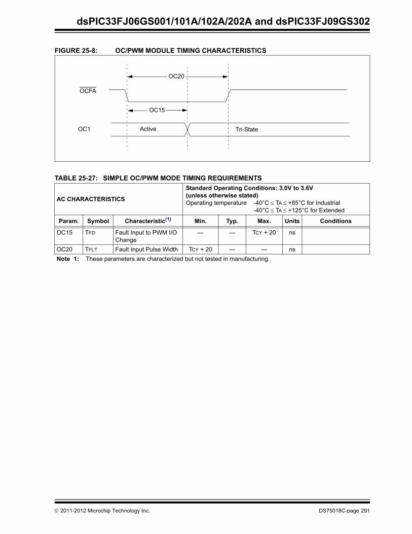
dsPIC33FJ06GS001/101A/102A/202A and dsPIC33FJ09GS302
FIGURE 25-8: OC/PWM MODULE TIMING CHARACTERISTICS
TABLE 25-27: SIMPLE OC/PWM MODE TIMING REQUIREMENTS
AC CHARACTERISTICS
Standard Operating Conditions: 3.0V to 3.6V(unless otherwise stated)Operating temperature -40°C TA +85°C for Industrial
-40°C TA +125°C for Extended
Param. Symbol Characteristic(1) Min. Typ. Max. Units Conditions
OC15 TFD Fault Input to PWM I/O Change
— — TCY + 20 ns
OC20 TFLT Fault Input Pulse Width TCY + 20 — — ns
Note 1: These parameters are characterized but not tested in manufacturing.
OCFA
OC1
OC20
OC15
Active Tri-State
2011-2012 Microchip Technology Inc. DS75018C-page 291

dsPIC33FJ06GS001/101A/102A/202A and dsPIC33FJ09GS302
FIGURE 25-9: HIGH-SPEED PWM MODULE FAULT TIMING CHARACTERISTICS
FIGURE 25-10: HIGH-SPEED PWM MODULE TIMING CHARACTERISTICS
TABLE 25-28: HIGH-SPEED PWM MODULE TIMING REQUIREMENTS
AC CHARACTERISTICS
Standard Operating Conditions: 3.0V to 3.6V(unless otherwise stated)Operating temperature -40°C TA +85°C for Industrial
-40°C TA +125°C for Extended
Param. Symbol Characteristic(1) Min. Typ. Max. Units Conditions
MP10 TFPWM PWM Output Fall Time — 2.5 — ns
MP11 TRPWM PWM Output Rise Time — 2.5 — ns
MP20TFD Fault Input to PWM
I/O Change— — 15 ns
MP30TFH Minimum PWM Fault Pulse
Width8 — — ns DTC<10> = 10
MP31 TPDLY Tap Delay 1.04 — — ns ACLK = 120 MHz
MP32 ACLK PWM Input Clock — — 120 MHz See Note 2, Note 3
Note 1: These parameters are characterized but not tested in manufacturing.
2: This parameter is a maximum allowed input clock for the PWM module.
3: The maximum value for this parameter applies to dsPIC33FJ06GS101A/102A/202A/302 devices only.
FLTx
PWMx
MP30
MP20
PWMx
Note: Refer to Figure 25-1 for load conditions.
MP11 MP10
DS75018C-page 292 2011-2012 Microchip Technology Inc.

dsPIC33FJ06GS001/101A/102A/202A and dsPIC33FJ09GS302
TABLE 25-29: SPIx MAXIMUM DATA/CLOCK RATE SUMMARY
FIGURE 25-11: SPIx MASTER MODE (HALF-DUPLEX, TRANSMIT ONLY, CKE = 0) TIMING CHARACTERISTICS
AC CHARACTERISTICS
Standard Operating Conditions: 3.0V to 3.6V(unless otherwise stated)Operating temperature -40°C TA +85°C for Industrial
-40°C TA +125°C for Extended
Maximum Data Rate
Master Transmit Only (Half-Duplex)
Master Transmit/Receive
(Full-Duplex)
Slave Transmit/Receive
(Full-Duplex)CKE CKP SMP
15 MHz Table 25-30 — — 0,1 0,1 0,1
9 MHz — Table 25-31 — 1 0,1 1
9 MHz — Table 25-32 — 0 0,1 1
15 MHz — — Table 25-33 1 0 0
11 MHz — — Table 25-34 1 1 0
15 MHz — — Table 25-35 0 1 0
11 MHz — — Table 25-36 0 0 0
SCKx(CKP = 0)
SCKx(CKP = 1)
SDOx
SP10
SP21SP20SP35
SP20SP21
MSb LSbBit 14 - - - - - -1
SP30, SP31SP30, SP31
Note: Refer to Figure 25-1 for load conditions.
2011-2012 Microchip Technology Inc. DS75018C-page 293

dsPIC33FJ06GS001/101A/102A/202A and dsPIC33FJ09GS302
FIGURE 25-12: SPIx MASTER MODE (HALF-DUPLEX, TRANSMIT ONLY, CKE = 1) TIMING CHARACTERISTICS
TABLE 25-30: SPIx MASTER MODE (HALF-DUPLEX, TRANSMIT ONLY) TIMING REQUIREMENTS
AC CHARACTERISTICS
Standard Operating Conditions: 3.0V to 3.6V(unless otherwise stated)Operating temperature -40°C TA +85°C for Industrial
-40°C TA +125°C for Extended
ParamNo.
Symbol Characteristic(1) Min Typ(2) Max Units Conditions
SP10 TscP Maximum SCKx Frequency — — 15 MHz See Note 3
SP20 TscF SCKx Output Fall Time — — — ns See Parameter DO32 and Note 4
SP21 TscR SCKx Output Rise Time — — — ns See Parameter DO31 and Note 4
SP30 TdoF SDOx Data Output Fall Time — — — ns See Parameter DO32 and Note 4
SP31 TdoR SDOx Data Output Rise Time — — — ns See Parameter DO31 and Note 4
SP35 TscH2doV,TscL2doV
SDOx Data Output Valid after SCKx Edge
— 6 20 ns
SP36 TdiV2scH,TdiV2scL
SDOx Data Output Setup to First SCKx Edge
30 — — ns
Note 1: These parameters are characterized, but are not tested in manufacturing.
2: Data in “Typ” column is at 3.3V, 25°C unless otherwise stated.
3: The minimum clock period for SCKx is 66.7 ns. Therefore, the clock generated in master mode must not violate this specification.
4: Assumes 50 pF load on all SPIx pins.
SCKx(CKP = 0)
SCKx(CKP = 1)
SDOx
SP21SP20SP35
SP20SP21
MSb LSbBit 14 - - - - - -1
SP30, SP31
Note: Refer to Figure 25-1 for load conditions.
SP36
SP10
DS75018C-page 294 2011-2012 Microchip Technology Inc.

dsPIC33FJ06GS001/101A/102A/202A and dsPIC33FJ09GS302
FIGURE 25-13: SPIx MASTER MODE (FULL-DUPLEX, CKE = 1, CKP = x, SMP = 1) TIMING CHARACTERISTICS
TABLE 25-31: SPIx MASTER MODE (FULL-DUPLEX, CKE = 1, CKP = x, SMP = 1) TIMING REQUIREMENTS
AC CHARACTERISTICS
Standard Operating Conditions: 3.0V to 3.6V(unless otherwise stated)Operating temperature -40°C TA +85°C for Industrial
-40°C TA +125°C for Extended
ParamNo.
Symbol Characteristic(1) Min Typ(2) Max Units Conditions
SP10 TscP Maximum SCKx Frequency — — 9 MHz See Note 3
SP20 TscF SCKx Output Fall Time — — — ns See Parameter DO32 and Note 4
SP21 TscR SCKx Output Rise Time — — — ns See Parameter DO31 and Note 4
SP30 TdoF SDOx Data Output Fall Time — — — ns See Parameter DO32 and Note 4
SP31 TdoR SDOx Data Output Rise Time — — — ns See Parameter DO31 and Note 4
SP35 TscH2doV,TscL2doV
SDOx Data Output Valid afterSCKx Edge
— 6 20 ns
SP36 TdoV2sc, TdoV2scL
SDOx Data Output Setup toFirst SCKx Edge
30 — — ns
SP40 TdiV2scH, TdiV2scL
Setup Time of SDIx Data Input to SCKx Edge
30 — — ns
SP41 TscH2diL, TscL2diL
Hold Time of SDIx Data Inputto SCKx Edge
30 — — ns
Note 1: These parameters are characterized, but are not tested in manufacturing.2: Data in “Typ” column is at 3.3V, 25°C unless otherwise stated.3: The minimum clock period for SCKx is 111 ns. The clock generated in master mode must not violate this
specification.4: Assumes 50 pF load on all SPIx pins.
SCKx(CKP = 0)
SCKx(CKP = 1)
SDOx
SP21SP20SP35
SP20SP21
MSb LSbBit 14 - - - - - -1
SP30, SP31
Note: Refer to Figure 25-1 for load conditions.
SP36
SP41
LSb InBit 14 - - - -1SDIx
SP40
SP10
MSb In
2011-2012 Microchip Technology Inc. DS75018C-page 295

dsPIC33FJ06GS001/101A/102A/202A and dsPIC33FJ09GS302
FIGURE 25-14: SPIx MASTER MODE (FULL-DUPLEX, CKE = 0, CKP = x, SMP = 1) TIMING CHARACTERISTICS
TABLE 25-32: SPIx MASTER MODE (FULL-DUPLEX, CKE = 0, CKP = x, SMP = 1) TIMING REQUIREMENTS
AC CHARACTERISTICS
Standard Operating Conditions: 3.0V to 3.6V(unless otherwise stated)Operating temperature -40°C TA +85°C for Industrial
-40°C TA +125°C for Extended
ParamNo.
Symbol Characteristic(1) Min Typ(2) Max Units Conditions
SP10 TscP Maximum SCKx Frequency — — 9 MHz -40ºC to +125ºC and see Note 3
SP20 TscF SCKx Output Fall Time — — — ns See Parameter DO32 and Note 4
SP21 TscR SCKx Output Rise Time — — — ns See Parameter DO31 and Note 4
SP30 TdoF SDOx Data Output Fall Time — — — ns See Parameter DO32 and Note 4
SP31 TdoR SDOx Data Output Rise Time — — — ns See Parameter DO31 and Note 4
SP35 TscH2doV,TscL2doV
SDOx Data Output Valid afterSCKx Edge
— 6 20 ns
SP36 TdoV2scH, TdoV2scL
SDOx Data Output Setup toFirst SCKx Edge
30 — — ns
SP40 TdiV2scH, TdiV2scL
Setup Time of SDIx Data Input to SCKx Edge
30 — — ns
SP41 TscH2diL, TscL2diL
Hold Time of SDIx Data Inputto SCKx Edge
30 — — ns
Note 1: These parameters are characterized, but are not tested in manufacturing.
2: Data in “Typ” column is at 3.3V, 25°C unless otherwise stated.
3: The minimum clock period for SCKx is 111 ns. The clock generated in master mode must not violate this specification.
4: Assumes 50 pF load on all SPIx pins.
SCKx(CKP = 0)
SCKx(CKP = 1)
SDOx
SDIx
SP10
SP40 SP41
SP21SP20SP35
SP20SP21
MSb LSbBit 14 - - - - - -1
LSb InBit 14 - - - -1
SP30, SP31SP30, SP31
Note: Refer to Figure 25-1 for load conditions.
MSb In
DS75018C-page 296 2011-2012 Microchip Technology Inc.

dsPIC33FJ06GS001/101A/102A/202A and dsPIC33FJ09GS302
FIGURE 25-15: SPIx SLAVE MODE (FULL-DUPLEX, CKE = 1, CKP = 0, SMP = 0) TIMING CHARACTERISTICS
SSx
SCKx(CKP = 0)
SCKx(CKP = 1)
SDOx
SP60
SDIx
SP30,SP31
MSb Bit 14 - - - - - -1 LSb
SP51
MSb In Bit 14 - - - -1 LSb In
SP35
SP52
SP73SP72
SP72SP73SP70
SP41
Note: Refer to Figure 25-1 for load conditions.
SP50
SP40
2011-2012 Microchip Technology Inc. DS75018C-page 297

dsPIC33FJ06GS001/101A/102A/202A and dsPIC33FJ09GS302
TABLE 25-33: SPIx SLAVE MODE (FULL-DUPLEX, CKE = 1, CKP = 0, SMP = 0) TIMING REQUIREMENTS
AC CHARACTERISTICS
Standard Operating Conditions: 3.0V to 3.6V(unless otherwise stated)Operating temperature -40°C TA +85°C for Industrial
-40°C TA +125°C for Extended
ParamNo.
Symbol Characteristic(1) Min Typ(2) Max Units Conditions
SP70 TscP Maximum SCKx Input Frequency — — 15 MHz See Note 3
SP72 TscF SCKx Input Fall Time — — — ns See Parameter DO32 and Note 4
SP73 TscR SCKx Input Rise Time — — — ns See Parameter DO31 and Note 4
SP30 TdoF SDOx Data Output Fall Time — — — ns See Parameter DO32 and Note 4
SP31 TdoR SDOx Data Output Rise Time — — — ns See Parameter DO31 and Note 4
SP35 TscH2doV,TscL2doV
SDOx Data Output Valid afterSCKx Edge
— 6 20 ns
SP36 TdoV2scH, TdoV2scL
SDOx Data Output Setup toFirst SCKx Edge
30 — — ns
SP40 TdiV2scH, TdiV2scL
Setup Time of SDIx Data Inputto SCKx Edge
30 — — ns
SP41 TscH2diL, TscL2diL
Hold Time of SDIx Data Inputto SCKx Edge
30 — — ns
SP50 TssL2scH, TssL2scL
SSx to SCKx or SCKx Input 120 — — ns
SP51 TssH2doZ SSx to SDOx OutputHigh-Impedance
10 — 50 ns See Note 4
SP52 TscH2ssHTscL2ssH
SSx after SCKx Edge 1.5 TCY + 40 — — ns See Note 4
SP60 TssL2doV SDOx Data Output Valid after SSx Edge
— — 50 ns
Note 1: These parameters are characterized, but are not tested in manufacturing.
2: Data in “Typ” column is at 3.3V, 25°C unless otherwise stated.
3: The minimum clock period for SCKx is 66.7 ns. Therefore, the SCKx clock generated by the master must not violate this specification.
4: Assumes 50 pF load on all SPIx pins.
DS75018C-page 298 2011-2012 Microchip Technology Inc.

dsPIC33FJ06GS001/101A/102A/202A and dsPIC33FJ09GS302
FIGURE 25-16: SPIx SLAVE MODE (FULL-DUPLEX, CKE = 1, CKP = 1, SMP = 0) TIMING CHARACTERISTICS
SSx
SCKx(CKP = 0)
SCKx(CKP = 1)
SDOx
SP60
SDIx
SP30,SP31
MSb Bit 14 - - - - - -1 LSb
SP51
MSb In Bit 14 - - - -1 LSb In
SP35
SP52
SP52
SP73SP72
SP72SP73SP70
SP41
Note: Refer to Figure 25-1 for load conditions.
SP50
SP40
2011-2012 Microchip Technology Inc. DS75018C-page 299

dsPIC33FJ06GS001/101A/102A/202A and dsPIC33FJ09GS302
TABLE 25-34: SPIx SLAVE MODE (FULL-DUPLEX, CKE = 1, CKP = 1, SMP = 0) TIMING REQUIREMENTS
AC CHARACTERISTICS
Standard Operating Conditions: 3.0V to 3.6V(unless otherwise stated)Operating temperature -40°C TA +85°C for Industrial
-40°C TA +125°C for Extended
ParamNo.
Symbol Characteristic(1) Min Typ(2) Max Units Conditions
SP70 TscP Maximum SCKx Input Frequency — — 11 MHz See Note 3
SP72 TscF SCKx Input Fall Time — — — ns See Parameter DO32 and Note 4
SP73 TscR SCKx Input Rise Time — — — ns See Parameter DO31 and Note 4
SP30 TdoF SDOx Data Output Fall Time — — — ns See Parameter DO32 and Note 4
SP31 TdoR SDOx Data Output Rise Time — — — ns See Parameter DO31 and Note 4
SP35 TscH2doV,TscL2doV
SDOx Data Output Valid afterSCKx Edge
— 6 20 ns
SP36 TdoV2scH, TdoV2scL
SDOx Data Output Setup toFirst SCKx Edge
30 — — ns
SP40 TdiV2scH, TdiV2scL
Setup Time of SDIx Data Inputto SCKx Edge
30 — — ns
SP41 TscH2diL, TscL2diL
Hold Time of SDIx Data Inputto SCKx Edge
30 — — ns
SP50 TssL2scH, TssL2scL
SSx to SCKx or SCKx Input 120 — — ns
SP51 TssH2doZ SSx to SDOx OutputHigh-Impedance
10 — 50 ns See Note 4
SP52 TscH2ssHTscL2ssH
SSx after SCKx Edge 1.5 TCY + 40 — — ns See Note 4
SP60 TssL2doV SDOx Data Output Valid after SSx Edge
— — 50 ns
Note 1: These parameters are characterized, but are not tested in manufacturing.
2: Data in “Typ” column is at 3.3V, 25°C unless otherwise stated.
3: The minimum clock period for SCKx is 91 ns. Therefore, the SCKx clock generated by the master must not violate this specification.
4: Assumes 50 pF load on all SPIx pins.
DS75018C-page 300 2011-2012 Microchip Technology Inc.

dsPIC33FJ06GS001/101A/102A/202A and dsPIC33FJ09GS302
FIGURE 25-17: SPIx SLAVE MODE (FULL-DUPLEX CKE = 0, CKP = 1, SMP = 0) TIMING CHARACTERISTICS
SSX
SCKX(CKP = 0)
SCKX(CKP = 1)
SDOX
SP50
SP41
SP30,SP31 SP51
SP35
MSb LSbBit 14 - - - - - -1
Bit 14 - - - -1 LSb In
SP52
SP73SP72
SP72SP73SP70
Note: Refer to Figure 25-1 for load conditions.
SDIX
SP40
MSb In
2011-2012 Microchip Technology Inc. DS75018C-page 301

dsPIC33FJ06GS001/101A/102A/202A and dsPIC33FJ09GS302
TABLE 25-35: SPIx SLAVE MODE (FULL-DUPLEX, CKE = 0, CKP = 1, SMP = 0) TIMING REQUIREMENTS
AC CHARACTERISTICS
Standard Operating Conditions: 3.0V to 3.6V(unless otherwise stated)Operating temperature -40°C TA +85°C for Industrial
-40°C TA +125°C for Extended
ParamNo.
Symbol Characteristic(1) Min Typ(2) Max Units Conditions
SP70 TscP Maximum SCKx Input Frequency — — 15 MHz See Note 3
SP72 TscF SCKx Input Fall Time — — — ns See Parameter DO32 and Note 4
SP73 TscR SCKx Input Rise Time — — — ns See Parameter DO31 and Note 4
SP30 TdoF SDOx Data Output Fall Time — — — ns See Parameter DO32 and Note 4
SP31 TdoR SDOx Data Output Rise Time — — — ns See Parameter DO31 and Note 4
SP35 TscH2doV,TscL2doV
SDOx Data Output Valid afterSCKx Edge
— 6 20 ns
SP36 TdoV2scH, TdoV2scL
SDOx Data Output Setup toFirst SCKx Edge
30 — — ns
SP40 TdiV2scH, TdiV2scL
Setup Time of SDIx Data Inputto SCKx Edge
30 — — ns
SP41 TscH2diL, TscL2diL
Hold Time of SDIx Data Inputto SCKx Edge
30 — — ns
SP50 TssL2scH, TssL2scL
SSx to SCKx or SCKx Input 120 — — ns
SP51 TssH2doZ SSx to SDOx OutputHigh-Impedance
10 — 50 ns See Note 4
SP52 TscH2ssHTscL2ssH
SSx after SCKx Edge 1.5 TCY + 40 — — ns See Note 4
Note 1: These parameters are characterized, but are not tested in manufacturing.
2: Data in “Typ” column is at 3.3V, 25°C unless otherwise stated.
3: The minimum clock period for SCKx is 66.7 ns. Therefore, the SCKx clock generated by the master must not violate this specification.
4: Assumes 50 pF load on all SPIx pins.
DS75018C-page 302 2011-2012 Microchip Technology Inc.

dsPIC33FJ06GS001/101A/102A/202A and dsPIC33FJ09GS302
FIGURE 25-18: SPIx SLAVE MODE (FULL-DUPLEX, CKE = 0, CKP = 0, SMP = 0) TIMING CHARACTERISTICS
SSX
SCKX(CKP = 0)
SCKX(CKP = 1)
SDOX
SP50
SP41
SP30,SP31 SP51
SP35
MSb LSbBit 14 - - - - - -1
Bit 14 - - - -1 LSb In
SP52
SP73SP72
SP72SP73SP70
Note: Refer to Figure 25-1 for load conditions.
SDIX
SP40
MSb In
2011-2012 Microchip Technology Inc. DS75018C-page 303
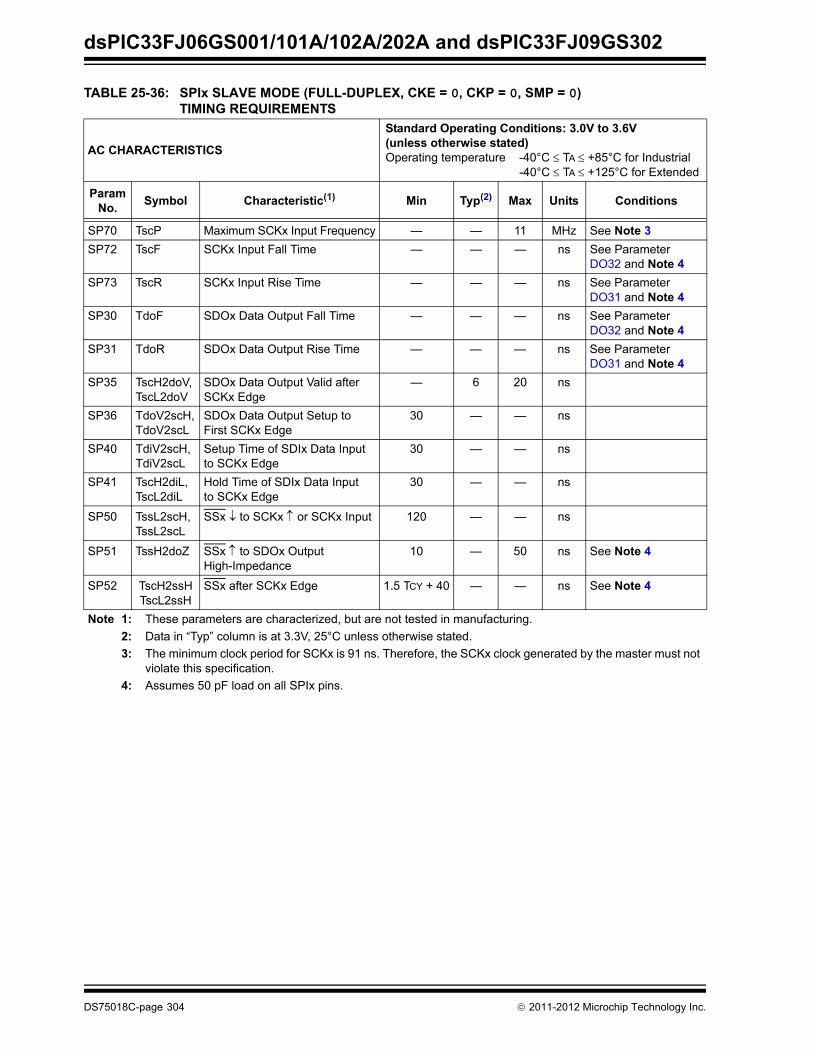
dsPIC33FJ06GS001/101A/102A/202A and dsPIC33FJ09GS302
TABLE 25-36: SPIx SLAVE MODE (FULL-DUPLEX, CKE = 0, CKP = 0, SMP = 0) TIMING REQUIREMENTS
AC CHARACTERISTICS
Standard Operating Conditions: 3.0V to 3.6V(unless otherwise stated)Operating temperature -40°C TA +85°C for Industrial
-40°C TA +125°C for Extended
ParamNo.
Symbol Characteristic(1) Min Typ(2) Max Units Conditions
SP70 TscP Maximum SCKx Input Frequency — — 11 MHz See Note 3
SP72 TscF SCKx Input Fall Time — — — ns See Parameter DO32 and Note 4
SP73 TscR SCKx Input Rise Time — — — ns See Parameter DO31 and Note 4
SP30 TdoF SDOx Data Output Fall Time — — — ns See Parameter DO32 and Note 4
SP31 TdoR SDOx Data Output Rise Time — — — ns See Parameter DO31 and Note 4
SP35 TscH2doV,TscL2doV
SDOx Data Output Valid afterSCKx Edge
— 6 20 ns
SP36 TdoV2scH, TdoV2scL
SDOx Data Output Setup toFirst SCKx Edge
30 — — ns
SP40 TdiV2scH, TdiV2scL
Setup Time of SDIx Data Inputto SCKx Edge
30 — — ns
SP41 TscH2diL, TscL2diL
Hold Time of SDIx Data Inputto SCKx Edge
30 — — ns
SP50 TssL2scH, TssL2scL
SSx to SCKx or SCKx Input 120 — — ns
SP51 TssH2doZ SSx to SDOx OutputHigh-Impedance
10 — 50 ns See Note 4
SP52 TscH2ssHTscL2ssH
SSx after SCKx Edge 1.5 TCY + 40 — — ns See Note 4
Note 1: These parameters are characterized, but are not tested in manufacturing.
2: Data in “Typ” column is at 3.3V, 25°C unless otherwise stated.
3: The minimum clock period for SCKx is 91 ns. Therefore, the SCKx clock generated by the master must not violate this specification.
4: Assumes 50 pF load on all SPIx pins.
DS75018C-page 304 2011-2012 Microchip Technology Inc.

dsPIC33FJ06GS001/101A/102A/202A and dsPIC33FJ09GS302
FIGURE 25-19: I2C1 BUS START/STOP BITS TIMING CHARACTERISTICS (MASTER MODE)
FIGURE 25-20: I2C1 BUS DATA TIMING CHARACTERISTICS (MASTER MODE)
SCL1
SDA1
StartCondition
StopCondition
Note: Refer to Figure 25-1 for load conditions.
IM30
IM31
IM33
IM34
IM11IM10 IM33
IM11
IM10
IM20
IM26IM25
IM40 IM40 IM45
IM21
SCL1
SDA1In
SDA1Out
Note: Refer to Figure 25-1 for load conditions.
2011-2012 Microchip Technology Inc. DS75018C-page 305

dsPIC33FJ06GS001/101A/102A/202A and dsPIC33FJ09GS302
TABLE 25-37: I2C1 BUS DATA TIMING REQUIREMENTS (MASTER MODE)
AC CHARACTERISTICS
Standard Operating Conditions: 3.0V to 3.6V(unless otherwise stated)Operating temperature -40°C TA +85°C for Industrial
-40°C TA +125°C for Extended
Param. Symbol Characteristic Min.(1) Max. Units Conditions
IM10 TLO:SCL Clock Low Time 100 kHz mode TCY/2 (BRG + 1) — s
400 kHz mode TCY/2 (BRG + 1) — s
1 MHz mode(2) TCY/2 (BRG + 1) — s
IM11 THI:SCL Clock High Time 100 kHz mode TCY/2 (BRG + 1) — s
400 kHz mode TCY/2 (BRG + 1) — s
1 MHz mode(2) TCY/2 (BRG + 1) — s
IM20 TF:SCL SDA1 and SCL1Fall Time
100 kHz mode — 300 ns CB is specified to be from 10 pF to 400 pF400 kHz mode 20 + 0.1 CB 300 ns
1 MHz mode(2) — 100 ns
IM21 TR:SCL SDA1 and SCL1Rise Time
100 kHz mode — 1000 ns CB is specified to be from 10 pF to 400 pF400 kHz mode 20 + 0.1 CB 300 ns
1 MHz mode(2) — 300 ns
IM25 TSU:DAT Data InputSetup Time
100 kHz mode 250 — ns
400 kHz mode 100 — ns
1 MHz mode(2) 40 — ns
IM26 THD:DAT Data InputHold Time
100 kHz mode 0 — s
400 kHz mode 0 0.9 s
1 MHz mode(2) 0.2 — s
IM30 TSU:STA Start ConditionSetup Time
100 kHz mode TCY/2 (BRG + 1) — s Only relevant for Repeated Startcondition
400 kHz mode TCY/2 (BRG + 1) — s
1 MHz mode(2) TCY/2 (BRG + 1) — s
IM31 THD:STA Start Condition Hold Time
100 kHz mode TCY/2 (BRG + 1) — s After this period thefirst clock pulse isgenerated
400 kHz mode TCY/2 (BRG + 1) — s
1 MHz mode(2) TCY/2 (BRG + 1) — s
IM33 TSU:STO Stop Condition Setup Time
100 kHz mode TCY/2 (BRG + 1) — s
400 kHz mode TCY/2 (BRG + 1) — s
1 MHz mode(2) TCY/2 (BRG + 1) — s
IM34 THD:STO Stop Condition 100 kHz mode TCY/2 (BRG + 1) — ns
Hold Time 400 kHz mode TCY/2 (BRG + 1) — ns
1 MHz mode(2) TCY/2 (BRG + 1) — ns
IM40 TAA:SCL Output Valid From Clock
100 kHz mode — 3500 ns
400 kHz mode — 1000 ns
1 MHz mode(2) — 400 ns
IM45 TBF:SDA Bus Free Time 100 kHz mode 4.7 — s Time the bus must be free before a newtransmission can start
400 kHz mode 1.3 — s
1 MHz mode(2) 0.5 — s
IM50 CB Bus Capacitive Loading — 400 pF
IM51 TPGD Pulse Gobbler Delay 65 390 ns See Note 3
Note 1: BRG is the value of the I2C™ Baud Rate Generator. Refer to Section 19. “Inter-Integrated Circuit (I2C™)” (DS70195) in the “dsPIC33F/PIC24H Family Reference Manual”.
2: Maximum pin capacitance = 10 pF for all I2C1 pins (for 1 MHz mode only).3: Typical value for this parameter is 130 ns.
DS75018C-page 306 2011-2012 Microchip Technology Inc.
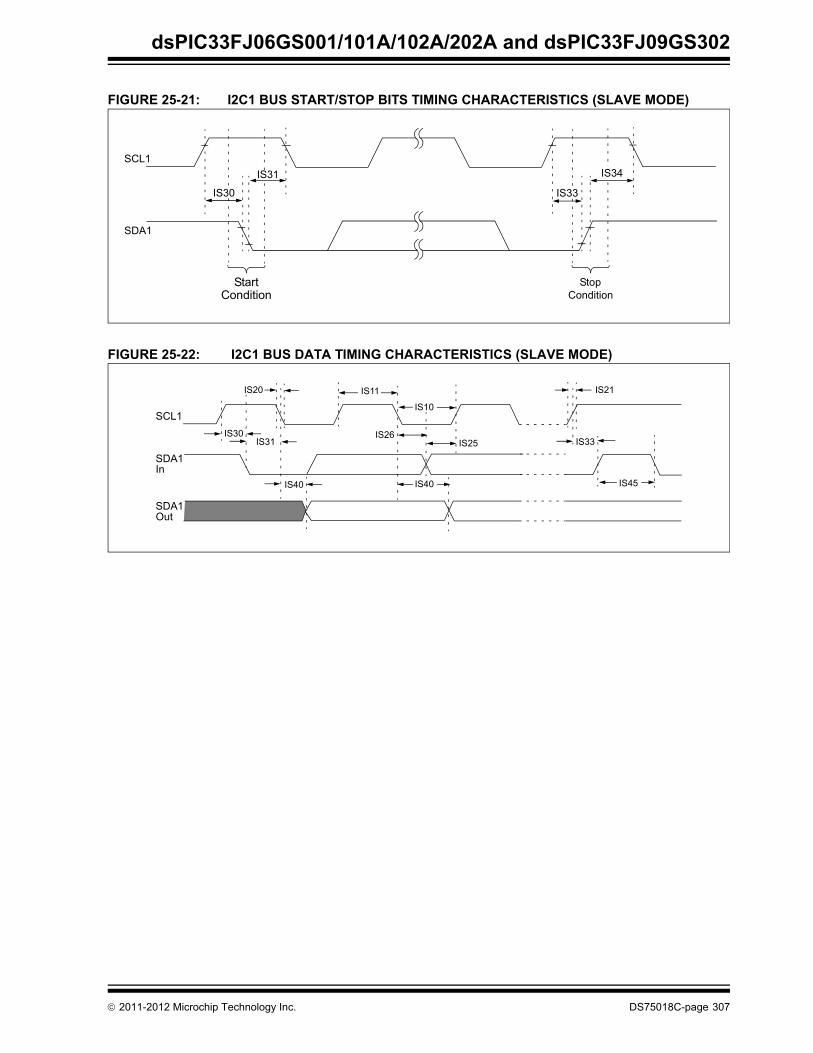
dsPIC33FJ06GS001/101A/102A/202A and dsPIC33FJ09GS302
FIGURE 25-21: I2C1 BUS START/STOP BITS TIMING CHARACTERISTICS (SLAVE MODE)
FIGURE 25-22: I2C1 BUS DATA TIMING CHARACTERISTICS (SLAVE MODE)
SCL1
SDA1
StartCondition
StopCondition
IS30
IS31
IS33
IS34
IS30IS31 IS33
IS11
IS10
IS20
IS26IS25
IS40 IS40 IS45
IS21
SCL1
SDA1In
SDA1Out
2011-2012 Microchip Technology Inc. DS75018C-page 307

dsPIC33FJ06GS001/101A/102A/202A and dsPIC33FJ09GS302
TABLE 25-38: I2C1 BUS DATA TIMING REQUIREMENTS (SLAVE MODE)
AC CHARACTERISTICS
Standard Operating Conditions: 3.0V to 3.6V(unless otherwise stated)Operating temperature -40°C TA +85°C for Industrial
-40°C TA +125°C for Extended
Param. Symbol Characteristic Min. Max. Units Conditions
IS10 TLO:SCL Clock Low Time 100 kHz mode 4.7 — s Device must operate at a minimum of 1.5 MHz
400 kHz mode 1.3 — s Device must operate at a minimum of 10 MHz
1 MHz mode(1) 0.5 — s
IS11 THI:SCL Clock High Time 100 kHz mode 4.0 — s Device must operate at a minimum of 1.5 MHz
400 kHz mode 0.6 — s Device must operate at a minimum of 10 MHz
1 MHz mode(2) 0.5 — s
IS20 TF:SCL SDA1 and SCL1Fall Time
100 kHz mode — 300 ns CB is specified to be from10 pF to 400 pF400 kHz mode 20 + 0.1 CB 300 ns
1 MHz mode(2) — 100 ns
IS21 TR:SCL SDA1 and SCL1Rise Time
100 kHz mode — 1000 ns CB is specified to be from10 pF to 400 pF400 kHz mode 20 + 0.1 CB 300 ns
1 MHz mode(2) — 300 ns
IS25 TSU:DAT Data InputSetup Time
100 kHz mode 250 — ns
400 kHz mode 100 — ns
1 MHz mode(2) 100 — ns
IS26 THD:DAT Data InputHold Time
100 kHz mode 0 — s
400 kHz mode 0 0.9 s
1 MHz mode(2) 0 0.3 s
IS30 TSU:STA Start ConditionSetup Time
100 kHz mode 4.7 — s Only relevant for Repeated Start condition400 kHz mode 0.6 — s
1 MHz mode(2) 0.25 — s
IS31 THD:STA Start Condition Hold Time
100 kHz mode 4.0 — s After this period, the first clock pulse is generated400 kHz mode 0.6 — s
1 MHz mode(2) 0.25 — s
IS33 TSU:STO Stop Condition Setup Time
100 kHz mode 4.7 — s
400 kHz mode 0.6 — s
1 MHz mode(2) 0.6 — s
IS34 THD:STO Stop ConditionHold Time
100 kHz mode 4000 — ns
400 kHz mode 600 — ns
1 MHz mode(2) 250 ns
IS40 TAA:SCL Output Valid From Clock
100 kHz mode 0 3500 ns
400 kHz mode 0 1000 ns
1 MHz mode(2) 0 350 ns
IS45 TBF:SDA Bus Free Time 100 kHz mode 4.7 — s Time the bus must be free before a new transmission can start
400 kHz mode 1.3 — s
1 MHz mode(2) 0.5 — s
IS50 CB Bus Capacitive Loading — 400 pF
Note 1: Maximum pin capacitance = 10 pF for all I2C1 pins (for 1 MHz mode only).
DS75018C-page 308 2011-2012 Microchip Technology Inc.

dsPIC33FJ06GS001/101A/102A/202A and dsPIC33FJ09GS302
=
TABLE 25-39: 10-BIT HIGH-SPEED ADC MODULE SPECIFICATIONS
AC CHARACTERISTICS(2)
Standard Operating Conditions: 3.0V and 3.6V(unless otherwise stated)Operating temperature -40°C TA +85°C for Industrial
-40°C TA +125°C for Extended
Param. Symbol Characteristic Min. Typ. Max. Units Conditions
Device Supply
AD01 AVDD Module VDD Supply — — — — AVDD is internally connected to VDD on 18-pin and 28-pin devices. See parameters (DC10) in Table 25-4.
AD02 AVSS Module VSS Supply — — — — AVSS is internally connected to VSS on 18-pin and 28-pin devices
Analog Input
AD10 VINH-VINL Full-Scale Input Span VSS — VDD V
AD11 VIN Absolute Input Voltage AVSS — AVDD V
AD12 IAD Operating Current — 8 — mA
AD13 — Leakage Current — ±0.6 — A VINL = AVSS = 0V,AVDD = 3.3V,Source Impedance = 100
AD17 RIN Recommended Impedanceof Analog Voltage Source
— — 100
DC Accuracy @ 1.5 Msps for 18 and 28-Pin Devices
AD20a Nr Resolution 10 data bits
AD21a INL Integral Nonlinearity -0.5 -0.3/+0.5 +1.2 LSb See Note 3
AD22a DNL Differential Nonlinearity -0.9 ±0.6 +0.9 LSb See Note 3
AD23a GERR Gain Error — 10 20 LSb See Note 3
AD24a EOFF Offset Error — 10 20 LSb See Note 3
AD25a — Monotonicity(1) — — — — Guaranteed
DC Accuracy @ 2.0 Msps for 18 and 28-Pin Devices
AD20b Nr Resolution 10 data bits
AD21b INL Integral Nonlinearity -1 ±1.5 +2.8 LSb
AD22b DNL Differential Nonlinearity -1.5 ±2 +2.8 LSb
AD23b GERR Gain Error — 10 20 LSb
AD24b EOFF Offset Error — 10 20 LSb
AD25b — Monotonicity(1) — — — — Guaranteed
DC Accuracy @ 2.0 Msps for 20 and 36-Pin Devices
AD20c Nr Resolution 10 data bits
AD21c INL Integral Nonlinearity > -2 ±0.5 < 2 LSb See Note 3
AD22c DNL Differential Nonlinearity > -1 ±0.5 < 1 LSb See Note 3
AD23c GERR Gain Error — 10 20 LSb See Note 3
AD24c EOFF Offset Error — 10 20 LSb See Note 3
AD25c — Monotonicity(1) — — — — Guaranteed
Note 1: The Analog-to-Digital conversion result never decreases with an increase in input voltage and has no missing codes.2: Overall functional device operation at VBORMIN < VDD < VDDMIN is tested but not characterized. All device analog
modules, such as the ADC, etc., will function, but with degraded performance below VDDMIN. Refer to Parameter BO10 in Table 25-11 for BOR values.
3: These parameters are characterized by similarity, but are not tested in manufacturing.
2011-2012 Microchip Technology Inc. DS75018C-page 309

dsPIC33FJ06GS001/101A/102A/202A and dsPIC33FJ09GS302
FIGURE 25-23: ANALOG-TO-DIGITAL CONVERSION TIMING PER INPUT
Dynamic Performance
AD30 THD Total Harmonic Distortion — -73 — dB
AD31 SINAD Signal to Noise and Distortion — 58 — dB
AD32 SFDR Spurious Free Dynamic Range — -73 — dB
AD33 FNYQ Input Signal Bandwidth — — 1 MHz
AD34 ENOB Effective Number of Bits — 9.4 — bits
TABLE 25-39: 10-BIT HIGH-SPEED ADC MODULE SPECIFICATIONS (CONTINUED)
AC CHARACTERISTICS(2)
Standard Operating Conditions: 3.0V and 3.6V(unless otherwise stated)Operating temperature -40°C TA +85°C for Industrial
-40°C TA +125°C for Extended
Param. Symbol Characteristic Min. Typ. Max. Units Conditions
Note 1: The Analog-to-Digital conversion result never decreases with an increase in input voltage and has no missing codes.2: Overall functional device operation at VBORMIN < VDD < VDDMIN is tested but not characterized. All device analog
modules, such as the ADC, etc., will function, but with degraded performance below VDDMIN. Refer to Parameter BO10 in Table 25-11 for BOR values.
3: These parameters are characterized by similarity, but are not tested in manufacturing.
TABLE 25-40: 10-BIT HIGH-SPEED ADC MODULE TIMING REQUIREMENTS
AC CHARACTERISTICS
Standard Operating Conditions: 3.0V to 3.6V(unless otherwise stated)Operating temperature -40°C TA +85°C for Industrial
-40°C TA +125°C for Extended
Param. Symbol Characteristic Min. Typ.(1) Max. Units Conditions
Clock Parameters
AD50b TAD ADC Clock Period 35.8 — — ns
Conversion Rate
AD55b tCONV Conversion Time — 14 TAD — —
AD56b FCNV Throughput Rate
Devices with Single SAR — — 2.0 Msps
Timing Parameters
AD63b tDPU Time to Stabilize Analog Stage from ADC Off to ADC On
1.0 — 10 s
Note 1: These parameters are characterized but not tested in manufacturing.
TAD
ADC Data
ADBUFxx
9 8 2 1 0
Old Data New Data
CONV
ADC Clock
Trigger Pulse
tCONV
DS75018C-page 310 2011-2012 Microchip Technology Inc.

dsPIC33FJ06GS001/101A/102A/202A and dsPIC33FJ09GS302
TABLE 25-41: HIGH-SPEED ANALOG COMPARATOR MODULE SPECIFICATIONS
DC CHARACTERISTICS(2)Standard Operating Conditions (unless otherwise stated)
Operating temperature: -40°C TA +85°C for Industrial-40°C TA +125°C for Extended
Param. Symbol Characteristic Min. Typ. Max. Units Comments
CM10 VIOFF Input Offset Voltage -58 +14/-40 66 mV
CM11 VICM Input Common-Mode Voltage Range(1)
0 — AVDD V
CM14 TRESP Large Signal Response 21 30 49 ns V+ input step of 100 mv while V- input held at AVDD/2. Delay measured from analog input pin to PWM output pin.
Note 1: These parameters are for design guidance only and are not tested in manufacturing.
2: Overall functional device operation at VBORMIN < VDD < VDDMIN is tested, but not characterized. All device analog modules, such as the ADC, etc., will function but with degraded performance below VDDMIN. Refer to Parameter BO10 in Table 25-11 for BOR values.
TABLE 25-42: DAC MODULE SPECIFICATIONS
AC and DC CHARACTERISTICS(2) Standard Operating Conditions (unless otherwise stated) Operating temperature: -40°C TA +85°C for Industrial
-40°C TA +125°C for Extended
Param. Symbol Characteristic Min. Typ. Max. Units Comments
DA01 EXTREF External Voltage Reference(1) 0 — AVDD – 1.6 V
DA08 INTREF Internal Voltage Reference(1) 1.15 1.25 1.35 V
DA02 CVRES Resolution 10 Bits
DA03 INL Integral Nonlinearity Error -7 -1 +7 LSB AVDD = 3.3V, DACREF = (AVDD/2)V
DA04 DNL Differential Nonlinearity Error -5 -0.5 +5 LSB
DA05 EOFF Offset Error 0.4 -0.8 2.6 %
DA06 EG Gain Error 0.4 -1.8 5.2 %
DA07 TSET Settling Time(1) 711 1551 2100 ns Measured when RANGE = 1 (high range) and the CMREF<9:0> bits transition from 0x1FF to 0x300
Note 1: Parameters are for design guidance only and are not tested in manufacturing.
2: Overall functional device operation at VBORMIN < VDD < VDDMIN is tested but not characterized. All device analog modules such as the ADC, etc., will function but with degraded performance below VDDMIN. Refer to Parameter BO10 in Table 25-11 for BOR values.
2011-2012 Microchip Technology Inc. DS75018C-page 311

dsPIC33FJ06GS001/101A/102A/202A and dsPIC33FJ09GS302
TABLE 25-44: DAC GAIN STAGE TO COMPARATOR SPECIFICATIONS
TABLE 25-43: DAC OUTPUT (DACOUT PIN) DC SPECIFICATIONS
DC CHARACTERISTICS(1)Standard Operating Conditions (unless otherwise stated)
Operating temperature: -40°C TA +85°C for Industrial-40°C TA +125°C for Extended
Param. Symbol Characteristic Min. Typ. Max. Units Comments
DA11 RLOAD Resistive Output Load Impedance
3K — — Ohm
— CLOAD Output Load Capacitance
— — 35 pF Including output pin capacitance
DA12 IOUT Output Current Drive Strength
200 300 — µA Sink and source
DA13 VRANGE Output Drive Voltage Range at Current Drive of 200 mA
AVSS + 250 mV — AVDD – 900 mV V
DA14 VLRANGE Output Drive Voltage Range at Reduced Current Drive of 50 mA
AVSS + 5 mV — AVDD – 500 mV V
DA15 IDD Current Consumed when Module Is Enabled
— — 1.3 x IOUT µA Module will always con-sume this current even if no load is connected to the output
DA16 ROUTON Output Impedance when Module is Enabled
— 820 — Ohms
DA30 VOFFSET Input Offset Voltage — 10 10 mV
Note 1: Overall functional device operation at VBORMIN < VDD < VDDMIN is tested but not characterized. All device analog modules, such as the ADC, etc., will function but with degraded performance below VDDMIN. Refer to Parameter BO10 in Table 25-11 for BOR values.
DC CHARACTERISTICS(1)
Standard Operating Conditions (unless otherwise stated)
Operating temperature: -40°C TA +85°C for Industrial-40°C TA +125°C for Extended
Param. Symbol Characteristic Min. Typ. Max. Units Conditions
DA15 IDD Current Consumed when Module Is Enabled.
— 60 — µA Module will always consume this current even if no load is connected to the output
DA32 G Amplifier Gain — 1.0 — —
— 1.8 — —
DA33 GBWP Gain Bandwidth Product — 2.0 — MHz At 1 pF load capacitance.Measured with sine wave output signal of 1V peak-to-peak with a midpoint value of 1.2V. Voltage excursion from 0.7 to 1.7V.
DA34 SR Slew Rate — 5 — V/µs Slew rate between 10% and 90% of AVDD
DA07 TS Settling Time — 200 — ns Settling time to 3%
Note 1: Overall functional device operation at VBORMIN < VDD < VDDMIN is tested but not characterized. All device analog modules, such as the ADC, etc., will function but with degraded performance below VDDMIN. Refer to Parameter BO10 in Table 25-11 for BOR values.
DS75018C-page 312 2011-2012 Microchip Technology Inc.
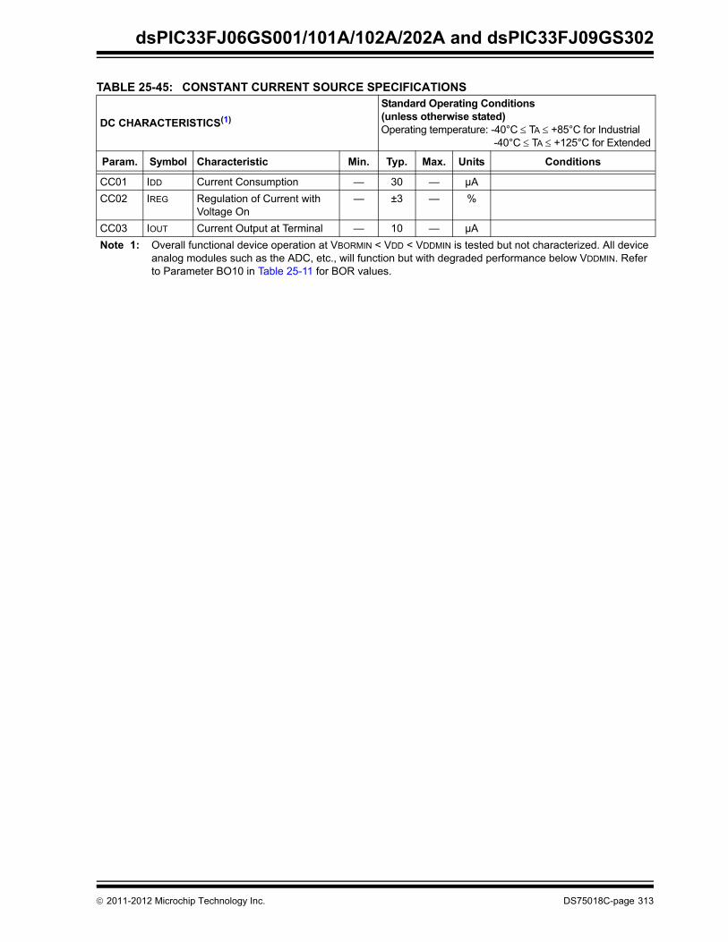
dsPIC33FJ06GS001/101A/102A/202A and dsPIC33FJ09GS302
TABLE 25-45: CONSTANT CURRENT SOURCE SPECIFICATIONS
DC CHARACTERISTICS(1)
Standard Operating Conditions (unless otherwise stated)
Operating temperature: -40°C TA +85°C for Industrial-40°C TA +125°C for Extended
Param. Symbol Characteristic Min. Typ. Max. Units Conditions
CC01 IDD Current Consumption — 30 — µA
CC02 IREG Regulation of Current with Voltage On
— ±3 — %
CC03 IOUT Current Output at Terminal — 10 — µA
Note 1: Overall functional device operation at VBORMIN < VDD < VDDMIN is tested but not characterized. All device analog modules such as the ADC, etc., will function but with degraded performance below VDDMIN. Refer to Parameter BO10 in Table 25-11 for BOR values.
2011-2012 Microchip Technology Inc. DS75018C-page 313

dsPIC33FJ06GS001/101A/102A/202A and dsPIC33FJ09GS302
NOTES:
DS75018C-page 314 2011-2012 Microchip Technology Inc.

2011
-2012 Microchip T
echnology Inc.
DS
75018C
-page 315
dsP
IC33F
J06GS
001/101A/102A
/202A an
d d
sPIC
33FJ09G
S302
26
FIG
FIG
VER PINS
IVER PINS
provided for design guidance purposesd may be outside the specified operating
2.00 3.00 4.00
VOL (V)
3V
3.3V
3.6V
e Maximum
2.00 3.00 4.00
VOL (V)
3V
3.3V
3.6V
e Maximum
.0 DC AND AC DEVICE CHARACTERISTICS GRAPHS
URE 26-1: VOH – 4x DRIVER PINS
URE 26-2: VOH – 16x DRIVER PINS
FIGURE 26-3: VOL – 4x DRI
FIGURE 26-4: VOL – 16x DR
Note: The graphs provided following this note are a statistical summary based on a limited number of samples and areonly. The performance characteristics listed herein are not tested or guaranteed. In some graphs, the data presenterange (e.g., outside specified power supply range) and therefore, outside the warranted range.
-0.030
-0.025
-0.020
-0.015
-0.010
IOH
(A)
-0.030
-0.025
-0.020
-0.015
-0.010
-0.005
0.0000.00 0.50 1.00 1.50 2.00 2.50 3.00 3.50 4.00
IOH
(A)
VOH (V)
3V
3.3V
3.6V
Absolute Maximum
-0.080
-0.070
-0.060
-0.050
-0.040
-0.030
-0.020
IOH
(A)
-0.080
-0.070
-0.060
-0.050
-0.040
-0.030
-0.020
-0.010
0.0000.00 1.00 2.00 3.00 4.00
IOH
(A)
VOH (V)
3.3V
3.6V
Absolute Maximum3V
0.010
0.015
0.020
0.025
0.030
0.035
0.040
IOL
(A)
0.000
0.005
0.010
0.015
0.020
0.025
0.030
0.035
0.040
0.00 1.00
IOL
(A)
Absolut
0.040
0.060
0.080
0.100
0.120
IOL
(A)
0.000
0.020
0.040
0.060
0.080
0.100
0.120
0.00 1.00
IOL
(A)
Absolut

dsP
IC33F
J06GS
001/101A/102A
/202A an
d d
sPIC
33FJ09G
S302
DS
75018C-page 316
2011-2012 M
icrochip Technolo
gy Inc.
IDD CURRENT @ VDD = 3.3V, +25ºC
IIDLE CURRENT @ VDD = 3.3V, +25ºC
MIPS
25 30 35 40
MIPS
25 30 35 40
FIGURE 26-5: TYPICAL IPD CURRENT @ VDD = 3.3V
FIGURE 26-6: TYPICAL IDOZE CURRENT @ VDD = 3.3V
FIGURE 26-7: TYPICAL
FIGURE 26-8: TYPICAL
IPD
Cu
rren
t (µ
A)
Temperature (Celsius)
0
50
100
150
200
250
300
350
400
450
-40 -20 0 20 40 60 80 100 120
IDO
ZE C
urr
ent
(mA
)
Doze Ratio
0
5
10
15
20
25
30
35
40
1 2 3 4 51:1 1:2 1:8 1:64 1:128
IDD
Cu
rre
nt
(mA
)
50
55
60
65
70
75
80
85
90
10 15 20
IIDL
E C
urr
ent
(mA
)
0
2
4
6
8
10
12
14
16
18
20
10 15 20
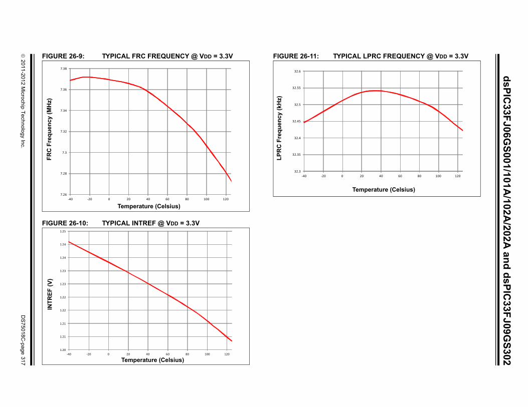
2011
-2012 Microchip T
echnology Inc.
DS
75018C
-page 317
dsP
IC33F
J06GS
001/101A/102A
/202A an
d d
sPIC
33FJ09G
S302
FIG
FIG
C FREQUENCY @ VDD = 3.3V
ature (Celsius)
40 60 80 100 120
URE 26-9: TYPICAL FRC FREQUENCY @ VDD = 3.3V
URE 26-10: TYPICAL INTREF @ VDD = 3.3V
FIGURE 26-11: TYPICAL LPRF
RC
Fre
qu
ency
(M
Hz)
Temperature (Celsius)
7.26
7.28
7.3
7.32
7.34
7.36
7.38
-40 -20 0 20 40 60 80 100 120
1.20
1.21
1.21
1.22
1.22
1.23
1.23
1.24
1.24
1.25
-40 -20 0 20 40 60 80 100 120
INT
RE
F (
V)
Temperature (Celsius)
LP
RC
Fre
qu
ency
(kH
z)
Temper
32.3
32.35
32.4
32.45
32.5
32.55
32.6
-40 -20 0 20

dsPIC33FJ06GS001/101A/102A/202A and dsPIC33FJ09GS302
NOTES:
DS75018C-page 318 2011-2012 Microchip Technology Inc.

dsPIC33FJ06GS001/101A/102A/202A and dsPIC33FJ09GS302
27.0 PACKAGING INFORMATION
27.1 Package Marking Information
Note: If the full Microchip part number cannot be marked on one line, it is carried over to the nextline, thus limiting the number of available characters for customer-specific information.
18-Lead SOIC (.300”)
XXXXXXXXXXXXXXXXXXXXXXXXXXXXXXXXXXXX
YYWWNNN
Example
dsPIC33FJ06
0830235
GS101-I/SO3e
18-Lead PDIP Example
XXXXXXXXXXXXXXXXXXXXXXXXXXXXXXXXXX
YYWWNNN
dsPIC30F3012
061001730I/P 3e
20-Lead SSOP
XXXXXXXXXXXXXXXXXXXXXX
YYWWNNN
Example
dsPIC33FJ12MC201-I/SS
0730235
3e
Legend: XX...X Customer-specific informationY Year code (last digit of calendar year)YY Year code (last 2 digits of calendar year)WW Week code (week of January 1 is week ‘01’)NNN Alphanumeric traceability code Pb-free JEDEC designator for Matte Tin (Sn)* This package is Pb-free. The Pb-free JEDEC designator ( )
can be found on the outer packaging for this package.
3e
3e
2011-2012 Microchip Technology Inc. DS75018C-page 319

dsPIC33FJ06GS001/101A/102A/202A and dsPIC33FJ09GS302
27.1 Package Marking Information (Continued)
Example
33FJJ16MC102E/MM0730235
3e
28-Lead SSOP
XXXXXXXXXXXXXXXXXXXXXXXX
YYWWNNN
Example
33FJ16MC102-E/SS
07302353e
36-Lead VTLA
XXXXXXXXXXXXXXXXYYWWNNN
Example
33FJJ16MC102E/TL0730235
3e
28-Lead SPDIP
XXXXXXXXXXXXXXXXXXXXXXXXXXXXXXXXXX
YYWWNNN
Example
dsPIC33FJ16MC
0730235
28-Lead SOIC
XXXXXXXXXXXXXXXXXXXXXXXXXXXXXXXXXXXXXXXXXXXXXXXXXXXXXXXXXXXX
YYWWNNN
Example
dsPIC33FJ16MC
0730235
102-E/SP
102-E/SO
3e
3e
28-Lead QFN-S
XXXXXXXXXXXXXXXXYYWWNNN
DS75018C-page 320 2011-2012 Microchip Technology Inc.
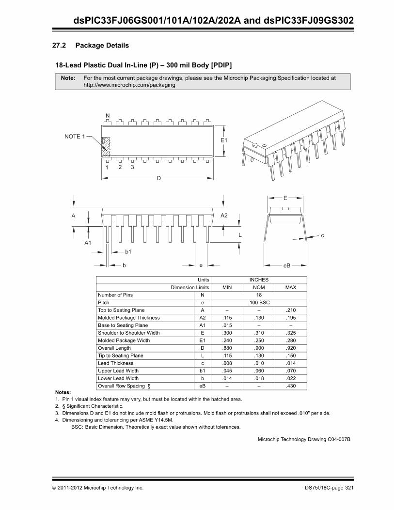
dsPIC33FJ06GS001/101A/102A/202A and dsPIC33FJ09GS302
27.2 Package Details
���������� ������������������������������
�
�� �� �� ������ �!"�����#�$�%��&"��'��� ��(�)"&�'"!&�)�����&�#�*�&����&�����&���#������� +������%����&�,����&��!&���-� ��'��!��!�����#�.��#��&�����"#��'�#�%��!����&"!��!����#�%��!����&"!��!�!������&��$���#�����/����!�#���� ��'��!��������#�&���������������.�0������
1�,2 1�!�����'��!���� ���&��������$��&� ��"��!�*��*�&�"&�&������!�
�� � 3�&���'!&��"��&����4����#�*���!(�����!��!���&��������������4�����������%���&������&�#��&��&&�255***�'��������'5���4�����
6��&! �7,8.���'��!���9�'�&! ��7 7:� ��;
7"')��%����! 7 �<��&�� � �����1�, ��&����&��������� � = = ������#�#����4���� ���4��!! �� ���� ��-� ����1�!��&����&��������� �� ���� = =��"�#��&���"�#��>�#&� . �-�� �-�� �-����#�#����4����>�#&� .� ���� ���� ��<�: �����9���&� � �<<� ���� ���� ���&����&��������� 9 ���� ��-� ����9��#� ���4��!! � ���< ���� ����6����9��#�>�#&� )� ���� ��?� ����9*��9��#�>�#&� ) ���� ���< ����: ������*����������+ �1 = = ��-�
NOTE 1
N
E1
D
1 2 3
A
A1
A2
L
E
eB
c
e
b1
b
������� ������� ��*��� ,������1
2011-2012 Microchip Technology Inc. DS75018C-page 321

dsPIC33FJ06GS001/101A/102A/202A and dsPIC33FJ09GS302
Note: For the most current package drawings, please see the Microchip Packaging Specification located at http://www.microchip.com/packaging
DS75018C-page 322 2011-2012 Microchip Technology Inc.

dsPIC33FJ06GS001/101A/102A/202A and dsPIC33FJ09GS302
Note: For the most current package drawings, please see the Microchip Packaging Specification located at http://www.microchip.com/packaging
2011-2012 Microchip Technology Inc. DS75018C-page 323

dsPIC33FJ06GS001/101A/102A/202A and dsPIC33FJ09GS302
Note: For the most current package drawings, please see the Microchip Packaging Specification located at http://www.microchip.com/packaging
DS75018C-page 324 2011-2012 Microchip Technology Inc.

dsPIC33FJ06GS001/101A/102A/202A and dsPIC33FJ09GS302
!��������� ��"#$��%"����&� �����""��'(���������""&�
�� �� �� ������ �!"�����#�$�%��&"��'��� ��(�)"&�'"!&�)�����&�#�*�&����&�����&���#������� ��'��!��!�����#�.��#��&�����"#��'�#�%��!����&"!��!����#�%��!����&"!��!�!������&��$���#������''����!�#��-� ��'��!��������#�&���������������.�0������
1�,2 1�!�����'��!���� ���&��������$��&� ��"��!�*��*�&�"&�&������!��.32 ��%��������'��!��(�"!"�����*�&�"&�&������(�%���%'�&����"�!�!�����
�� � 3�&���'!&��"��&����4����#�*���!(�����!��!���&��������������4�����������%���&������&�#��&��&&�255***�'��������'5���4�����
6��&! ��99��. .����'��!���9�'�&! ��7 7:� ��;
7"')��%����! 7 ����&�� � ��?��1�,: �����8����& � = = ������#�#����4���� ���4��!! �� ��?� ���� ��<��&��#%%� �� ���� = =: �����>�#&� . ���� ��<� <�����#�#����4����>�#&� .� ���� ��-� ��?�: �����9���&� � ?��� ���� ����3&�9���&� 9 ���� ���� ����3&���& 9� ������.39��#� ���4��!! � ���� = ����3&������ � �@ �@ <@9��#�>�#&� ) ���� = ��-<
φ
LL1
A2c
eb
A1
A
1 2
NOTE 1
E1
E
D
N
������� ������� ��*��� ,������1
2011-2012 Microchip Technology Inc. DS75018C-page 325

dsPIC33FJ06GS001/101A/102A/202A and dsPIC33FJ09GS302
Note: For the most current package drawings, please see the Microchip Packaging Specification located at http://www.microchip.com/packaging
DS75018C-page 326 2011-2012 Microchip Technology Inc.

dsPIC33FJ06GS001/101A/102A/202A and dsPIC33FJ09GS302
!��������� ��"#$��%"����&� �����""��'(���������""&�
�� �� �� ������ �!"�����#�$�%��&"��'��� ��(�)"&�'"!&�)�����&�#�*�&����&�����&���#������� ��'��!��!�����#�.��#��&�����"#��'�#�%��!����&"!��!����#�%��!����&"!��!�!������&��$���#������''����!�#��-� ��'��!��������#�&���������������.�0������
1�,2 1�!�����'��!���� ���&��������$��&� ��"��!�*��*�&�"&�&������!��.32 ��%��������'��!��(�"!"�����*�&�"&�&������(�%���%'�&����"�!�!�����
�� � 3�&���'!&��"��&����4����#�*���!(�����!��!���&��������������4�����������%���&������&�#��&��&&�255***�'��������'5���4�����
6��&! ��99��. .����'��!���9�'�&! ��7 7:� ��;
7"')��%����! 7 �<��&�� � ��?��1�,: �����8����& � = = ������#�#����4���� ���4��!! �� ��?� ���� ��<��&��#%%� �� ���� = =: �����>�#&� . ���� ��<� <�����#�#����4����>�#&� .� ���� ��-� ��?�: �����9���&� � ���� ����� �����3&�9���&� 9 ���� ���� ����3&���& 9� ������.39��#� ���4��!! � ���� = ����3&������ � �@ �@ <@9��#�>�#&� ) ���� = ��-<
LL1
cA2
A1
A
EE1
D
N
1 2
NOTE 1b
e
φ
������� ������� ��*��� ,�����-1
2011-2012 Microchip Technology Inc. DS75018C-page 327

dsPIC33FJ06GS001/101A/102A/202A and dsPIC33FJ09GS302
Note: For the most current package drawings, please see the Microchip Packaging Specification located at http://www.microchip.com/packaging
DS75018C-page 328 2011-2012 Microchip Technology Inc.

dsPIC33FJ06GS001/101A/102A/202A and dsPIC33FJ09GS302
Note: For the most current package drawings, please see the Microchip Packaging Specification located at http://www.microchip.com/packaging
2011-2012 Microchip Technology Inc. DS75018C-page 329

dsPIC33FJ06GS001/101A/102A/202A and dsPIC33FJ09GS302
Note: For the most current package drawings, please see the Microchip Packaging Specification located at http://www.microchip.com/packaging
DS75018C-page 330 2011-2012 Microchip Technology Inc.

dsPIC33FJ06GS001/101A/102A/202A and dsPIC33FJ09GS302
Note: For the most current package drawings, please see the Microchip Packaging Specification located at http://www.microchip.com/packaging
2011-2012 Microchip Technology Inc. DS75018C-page 331

dsPIC33FJ06GS001/101A/102A/202A and dsPIC33FJ09GS302
!������"%������� ��������������"�������������"���
�� �� �� ������ �!"�����#�$�%��&"��'��� ��(�)"&�'"!&�)�����&�#�*�&����&�����&���#������� +������%����&�,����&��!&���-� ��'��!��!�����#�.��#��&�����"#��'�#�%��!����&"!��!����#�%��!����&"!��!�!������&��$���#�����/����!�#���� ��'��!��������#�&���������������.�0������
1�,2 1�!�����'��!���� ���&��������$��&� ��"��!�*��*�&�"&�&������!�
�� � 3�&���'!&��"��&����4����#�*���!(�����!��!���&��������������4�����������%���&������&�#��&��&&�255***�'��������'5���4�����
6��&! �7,8.���'��!���9�'�&! ��7 7:� ��;
7"')��%����! 7 �<��&�� � �����1�, ��&����&��������� � = = ������#�#����4���� ���4��!! �� ���� ��-� ����1�!��&����&��������� �� ���� = =��"�#��&���"�#��>�#&� . ���� �-�� �--���#�#����4����>�#&� .� ���� ��<� ����: �����9���&� � ��-�� ��-?� ����� ���&����&��������� 9 ���� ��-� ����9��#� ���4��!! � ���< ���� ����6����9��#�>�#&� )� ���� ���� ����9*��9��#�>�#&� ) ���� ���< ����: ������*����������+ �1 = = ��-�
NOTE 1
N
1 2
D
E1
eB
c
E
L
A2
eb
b1A1
A
3
������� ������� ��*��� ,������1
DS75018C-page 332 2011-2012 Microchip Technology Inc.

dsPIC33FJ06GS001/101A/102A/202A and dsPIC33FJ09GS302
2011-2012 Microchip Technology Inc. DS75018C-page 333

dsPIC33FJ06GS001/101A/102A/202A and dsPIC33FJ09GS302
DS75018C-page 334 2011-2012 Microchip Technology Inc.
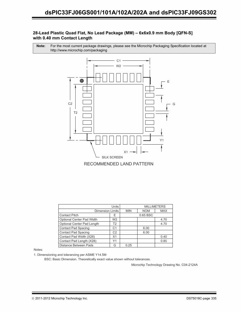
dsPIC33FJ06GS001/101A/102A/202A and dsPIC33FJ09GS302
!��������� ��)���*�� +��������%�,��--��././�(0�������)*��"�1� #�(2���3�� �� ���, #
�� � 3�&���'!&��"��&����4����#�*���!(�����!��!���&��������������4�����������%���&������&�#��&��&&�255***�'��������'5���4�����
2011-2012 Microchip Technology Inc. DS75018C-page 335

dsPIC33FJ06GS001/101A/102A/202A and dsPIC33FJ09GS302
DS75018C-page 336 2011-2012 Microchip Technology Inc.

dsPIC33FJ06GS001/101A/102A/202A and dsPIC33FJ09GS302
2011-2012 Microchip Technology Inc. DS75018C-page 337

dsPIC33FJ06GS001/101A/102A/202A and dsPIC33FJ09GS302
NOTES:
DS75018C-page 338 2011-2012 Microchip Technology Inc.

dsPIC33FJ06GS001/101A/102A/202A and dsPIC33FJ09GS302
APPENDIX A: REVISION HISTORY
Revision A (July 2011)
This is the initial released version of this document.
Revision B (February 2012)
This revision includes formatting changes and minortypographical updates throughout the data sheet text.
Where applicable, new sections were added to eachperipheral chapter that provide information and links torelated resources, as well as helpful tips. Forexamples, see Section 18.1 “UART Helpful Tips”and Section 18.1 “UART Helpful Tips”.
The data sheet status was updated from AdvanceInformation to Preliminary.
In addition, all occurrences to the package known asTLA were updated to VTLA.
All other major changes are referenced by theirrespective section in Table A-1.
TABLE A-1: MAJOR SECTION UPDATES
Section Name Update Description
“16-Bit Microcontrollers and Digital Signal Controllers with High-Speed PWM, ADC and Comparators”
The previous content was reorganized and is now presented as the first page of the data sheet.
Relocated the Referenced Sources content, which was previously presented in Section 1.0 “Device Overview”.
Section 2.0 “Guidelines for Getting Started with 16-Bit Digital Signal Controllers”
Updated the Recommended Minimum Connection diagram (see Figure 2-1).
Section 4.0 “Memory Organization”
Updated the Program Memory Map (see Figure 4-1).
Updated bits 10-8 in IPC27 of the Interrupt Controller Register Map for dsPIC33FJ06GS001 Devices (see Table 4-4).
Renamed the CHOPCLK<6:0> bits in the CHOP register to: CHOP<6:0> in the High-Speed PWM Register Map (see Table 4-12).
Removed RPINR11 from the Peripheral Pin Select Input Register Map for the dsPIC33FJ06GS001 Device (see Table 4-24).
Added the REFOMD bit to PMD4 in the PMD Register Map for the dsPIC33FJ06GS001 device (see Table 4-34).
Section 21.0 “Constant Current Source”
Added the Current Source Calibration bits (ISRCCAL<5:0>) to the Current Source Control register (see Register 21-1).
Section 22.0 “Special Features” Added the Constant Current Source Calibration Register (see Register 22-1).
Section 25.0 “Electrical Characteristics”
Updated the Absolute Maximum Ratings(1).
Added Note 1 to the Operating MIPS vs. Voltage specification (see Table 25-1).
Updated all DC Characteristics: I/O Pin Output Specifications (see Table 25-10).
Updated the typical value for Parameters F20a and F20b in the Internal FRC Accuracy specification (see Table 25-19).
Updated the minimum and maximum values for Parameter TA20, and the minimum value for Parameter TA11 in the Timer1 External Clock Timing Requirements (see Table 25-23).
Updated the OC/PWM Module Timing Characteristics diagram (see Figure 25-8).
Updated the minimum and maximum values for the Simple OC/PWM Mode Timing Requirements (see Table 25-27).
Added Note 4 and Note 5 to the 10-Bit, High-Speed ADC Module Specifications (see Table 25-39).
Section 26.0 “DC and AC Device Characteristics Graphs”
Added new chapter.
2011-2012 Microchip Technology Inc. DS75018C-page 339

dsPIC33FJ06GS001/101A/102A/202A and dsPIC33FJ09GS302
Revision C (August 2012)
This revision includes minor typographical updates andcontent corrections. Major changes include new figuresin Section 26.0 “DC and AC Device CharacteristicsGraphs”, updated values in Table 25-39 in Section 25.0“Electrical Characteristics” and updated packagedrawings in Section 27.0 “Packaging Information”.
DS75018C-page 340 2011-2012 Microchip Technology Inc.

dsPIC33FJ06GS001/101A/102A/202A and dsPIC33FJ09GS302
INDEX
AAC Characteristics ............................................................ 282
Internal LPRC Accuracy............................................ 285Internal RC Accuracy ................................................ 285Load Conditions ........................................................ 282Temperature and Voltage Specifications .................. 282
Alternate Interrupt Vector Table (AIVT) .............................. 87Arithmetic Logic Unit (ALU)................................................. 31Assembler
MPASM Assembler................................................... 268Auxiliary Clock Generation................................................ 125
BBit-Reversed Addressing .................................................... 69
Example ...................................................................... 70Implementation ........................................................... 69Sequence Table (16-Entry)......................................... 70
Block Diagrams16-Bit Timer1 Module................................................ 173Boost Converter Implementation ................................ 21Connections for On-Chip Voltage Regulator............. 256Constant Current Source .......................................... 249CPU Core.................................................................... 26Digital PFC.................................................................. 21DSP Engine ................................................................ 32dsPIC33FJ06GS001 Device ADC ............................ 226dsPIC33FJ06GS001/101A/102A/202A and
dsPIC33FJ09GS302........................................... 14dsPIC33FJ06GS101A Device ADC .......................... 227dsPIC33FJ06GS102A Device ADC .......................... 228dsPIC33FJ06GS202A Device ADC .......................... 229dsPIC33FJ09GS302 Device ADC ............................ 230High-Speed Analog Comparator............................... 243Hysteresis Control..................................................... 245I2C............................................................................. 212Input Capture ............................................................ 177Interleaved PFC.......................................................... 22MCLR Pin Connections............................................... 18Multiplexing of Remappable Output for RPn............. 150Oscillator System...................................................... 123Output Compare ....................................................... 179Partitioned Output Pair, Complementary
PWM Mode ....................................................... 186Phase-Shifted Full-Bridge Converter .......................... 23PLL............................................................................ 125Recommended Minimum Connection......................... 18Remappable MUX Input for U1RX............................ 148Reset System.............................................................. 79Shared Port Structure ............................................... 146Simplified Conceptual High-Speed PWM ................. 185Single-Phase Synchronous Buck Converter............... 22SPI ............................................................................ 205Type B Timer2 .......................................................... 175UART ........................................................................ 219Watchdog Timer (WDT) ............................................ 257
Brown-out Reset (BOR) ............................................ 251, 256
CC Compilers
MPLAB C18.............................................................. 268Capacitor on Internal Voltage Regulator (VCAP)................. 18Clock Switching ................................................................ 134
Enabling.................................................................... 134Sequence ................................................................. 134
Code ExamplesPort Write/Read ........................................................ 147PWRSAV Instruction Syntax .................................... 137
Code Protection................................................................ 251Configuration Bits ............................................................. 251
Description................................................................ 254Configuring Analog Port Pins............................................ 147Constant Current Source
Description................................................................ 249Features ................................................................... 249
CPUBarrel Shifter............................................................... 35Control Registers........................................................ 28Data Addressing Overview ......................................... 25DSP Engine Overview ................................................ 25MCU Special Features ............................................... 26Special Features....................................................... 251
CPU Clocking System ...................................................... 124PLL Configuration..................................................... 125Selection................................................................... 124Sources .................................................................... 124
Customer Change Notification Service............................. 346Customer Notification Service .......................................... 346Customer Support............................................................. 346
DDAC .................................................................................. 244
Buffer Gain ............................................................... 244Output Range ........................................................... 245
Data Accumulators and Adder/Subtracter .......................... 33Data Space Write Saturation ...................................... 35Overflow and Saturation ............................................. 33Round Logic ............................................................... 34Write Back .................................................................. 34
Data Address Space........................................................... 39Alignment.................................................................... 39Memory Map for Devices with 1 Kbyte of RAM .......... 41Memory Map for Devices with 256 Bytes of RAM ...... 40Near Data Space ........................................................ 39Software Stack ........................................................... 66Width .......................................................................... 39X and Y Data .............................................................. 42
DC and AC CharacteristicsGraphs and Tables ................................................... 315
DC CharacteristicsDoze Current (IDOZE)................................................ 277I/O Pin Input Specifications ...................................... 278I/O Pin Output Specifications.................................... 280Idle Current (IIDLE) .................................................... 275Operating Current (IDD) ............................................ 274Operating MIPS vs. Voltage ..................................... 272Power-Down Current (IPD)........................................ 276Program Memory...................................................... 281Temperature and Voltage Specifications.................. 273
2011-2012 Microchip Technology Inc. DS75018C-page 341

dsPIC33FJ06GS001/101A/102A/202A and dsPIC33FJ09GS302
DC SpecificationsDAC Output (DACOUT Pin) ...................................... 312
Development Support ....................................................... 267Doze Mode........................................................................ 138DSC Guidelines................................................................... 17
Basic Connection Requirements................................. 17Decoupling Capacitors................................................ 17
DSP Engine......................................................................... 31Multiplier...................................................................... 33
EElectrical Characteristics................................................... 271
Absolute Maximum Ratings ...................................... 271Equations
Device Operating Frequency .................................... 124FOSC Calculation....................................................... 125Maximum Page Erase Time........................................ 76Minimum Page Erase Time......................................... 76XT with PLL Mode Example...................................... 125
Errata .................................................................................. 11
FFail-Safe Clock Monitor (FSCM) ....................................... 135Flash Program Memory....................................................... 75
Control Registers ........................................................ 76Operations .................................................................. 76Table Instructions........................................................ 75
Flexible Configuration ....................................................... 251
HHigh-Speed 10-Bit ADC .................................................... 225
Description ................................................................ 225Features.................................................................... 225Functionality .............................................................. 225
High-Speed Analog Comparator ....................................... 243Applications............................................................... 244Control Registers ...................................................... 245DAC .......................................................................... 244Digital Logic .............................................................. 244Hysteresis ................................................................. 245Input Range .............................................................. 244Interaction with I/O Buffers........................................ 245
High-Speed PWM ............................................................. 183Control Registers ...................................................... 186
II/O Ports ............................................................................ 145
Helpful Tips ............................................................... 152Parallel I/O (PIO)....................................................... 145Resources................................................................. 152Write/Read Timing .................................................... 147
I2COperating Modes ...................................................... 211Registers................................................................... 213
In-Circuit Debugger ........................................................... 258In-Circuit Emulation........................................................... 251In-Circuit Serial Programming (ICSP) ....................... 251, 258
Analog, Digital Pins Configuration .............................. 20Pins ............................................................................. 19
Input Capture .................................................................... 177Input Change Notification.................................................. 147
Instruction Addressing Modes ............................................ 66File Register Instructions ............................................ 66Fundamental Modes Supported ................................. 67MAC Instructions ........................................................ 67MCU Instructions ........................................................ 66Move and Accumulator Instructions............................ 67Other Instructions ....................................................... 67
Instruction SetOverview................................................................... 262Summary .................................................................. 259
Instruction-Based Power-Saving Modes........................... 137Idle............................................................................ 138Sleep ........................................................................ 137
Interfacing Program and Data Memory Spaces.................. 71Internal RC Oscillator
Use with WDT........................................................... 257Internet Address ............................................................... 346Interrupt Control and Status Registers ............................... 90
IECx............................................................................ 90IFSx ............................................................................ 90INTCON1.................................................................... 90INTCON2.................................................................... 90INTTREG.................................................................... 90IPCx............................................................................ 90
Interrupt Setup Procedures............................................... 122Initialization............................................................... 122Interrupt Disable ....................................................... 122Interrupt Service Routine.......................................... 122Trap Service Routine................................................ 122
Interrupt Vector Table (IVT) ................................................ 87Interrupts Coincident with Power Save Instructions ......... 138
JJTAG Boundary Scan Interface ........................................ 251JTAG Interface.................................................................. 258
LLEBCONx (PWMx Leading-Edge Blanking Control) ........ 202
MMaster Clear (MCLR).......................................................... 18Memory Organization ......................................................... 37Microchip Internet Web Site.............................................. 346Modulo Addressing ............................................................. 68
Applicability................................................................. 69Operation Example..................................................... 68Start and End Address ............................................... 68W Address Register Selection.................................... 68
MPLAB ASM30 Assembler, Linker, Librarian ................... 268MPLAB Integrated Development
Environment Software .............................................. 267MPLAB PM3 Device Programmer .................................... 270MPLAB REAL ICE In-Circuit Emulator System ................ 269MPLINK Object Linker/MPLIB Object Librarian ................ 268
OOpen-Drain Configuration................................................. 147Oscillator
External Pins .............................................................. 19Value Conditions on Start-up...................................... 20
Oscillator Configuration .................................................... 123Output Compare ............................................................... 179
DS75018C-page 342 2011-2012 Microchip Technology Inc.

dsPIC33FJ06GS001/101A/102A/202A and dsPIC33FJ09GS302
PPackaging ......................................................................... 319
Details ....................................................................... 321Marking ..................................................................... 319
Peripheral Module Disable (PMD) .................................... 138Peripheral Pin Select (PPS).............................................. 148
Registers................................................................... 153Pinout I/O Descriptions ....................................................... 15Power-on Reset (POR) ....................................................... 84Power-Saving Features .................................................... 137
Clock Frequency and Switching................................ 137Program Address Space..................................................... 37
Construction................................................................ 71Data Access from Program Memory Using
Program Space Visibility ..................................... 74Data Access from Program Memory Using
Table Instructions ............................................... 73Data Access from, Address Generation...................... 72Memory Maps ............................................................. 37Table Read Instructions
TBLRDH ............................................................. 73TBLRDL .............................................................. 73
Visibility Operation ...................................................... 74Program Memory
Interrupt Vector ........................................................... 38Organization................................................................ 38Reset Vector ............................................................... 38
Pseudo-Random Generator .............................................. 135
RReader Response ............................................................. 347Reference Clock Generation............................................. 125Register Maps
Configuration Flash Bytes (dsPIC33FJ06GS001/101A/X02A) ................... 252
Configuration Flash Bytes (dsPIC33FJ09GS302) ...................................... 252
RegistersACLKCON (Auxiliary Clock Divisor Control) ............. 131ADCON (ADC Control) ............................................. 231ADCPC0 (ADC Convert Pair Control 0).................... 236ADCPC1 (ADC Convert Pair Control 1).................... 238ADCPC3 (ADC Convert Pair Control 3).................... 240ADPCFG (ADC Port Configuration) .......................... 235ADSTAT (ADC Status).............................................. 233ALTDTRx (PWMx Alternate Dead-Time) .................. 195AUXCONx (PWM Auxiliary Control) ......................... 204CHOP (PWM Chop Clock Generator)....................... 203CLKDIV (Clock Divisor)............................................. 128CMPCONx (Comparator Control x) .......................... 246CMPDACx (Comparator DAC Control x) .................. 248Constant Current Source Calibration ........................ 253CORCON (Core Control) ...................................... 30, 91DTRx (PWMx Dead-Time) ........................................ 195FCLCONx (PWMx Fault Current-Limit Control) ........ 199I2C1CON (I2C1 Control)........................................... 213I2C1MSK (I2C1 Slave Mode Address Mask)............ 217I2C1STAT (I2C1 Status) ........................................... 215IC1CON (Input Capture 1 Control)............................ 178IEC0 (Interrupt Enable Control 0) ............................. 101IEC1 (Interrupt Enable Control 1) ............................. 102IEC3 (Interrupt Enable Control 3) ............................. 103IEC4 (Interrupt Enable Control 4) ............................. 103IEC5 (Interrupt Enable Control 5) ............................. 104IEC6 (Interrupt Enable Control 6) ............................. 105IEC7 (Interrupt Enable Control 7) ............................. 106
IFS0 (Interrupt Flag Status 0) ..................................... 95IFS1 (Interrupt Flag Status 1) ..................................... 96IFS3 (Interrupt Flag Status 3) ..................................... 97IFS4 (Interrupt Flag Status 4) ..................................... 97IFS5 (Interrupt Flag Status 5) ..................................... 98IFS6 (Interrupt Flag Status 6) ..................................... 99IFS7 (Interrupt Flag Status 7) ................................... 100INTCON1 (Interrupt Control 1) ................................... 92INTCON2 (Interrupt Control 2) ................................... 94INTTREG (Interrupt Control and Status) .................. 121IOCONx (PWMx I/O Control).................................... 197IPC0 (Interrupt Priority Control 0) ............................. 107IPC1 (Interrupt Priority Control 1) ............................. 108IPC14 (Interrupt Priority Control 14) ......................... 113IPC16 (Interrupt Priority Control 16) ......................... 113IPC2 (Interrupt Priority Control 2) ............................. 109IPC20 (Interrupt Priority Control 20) ......................... 114IPC23 (Interrupt Priority Control 23) ......................... 115IPC24 (Interrupt Priority Control 24) ......................... 116IPC25 (Interrupt Priority Control 25) ......................... 117IPC27 (Interrupt Priority Control 27) ......................... 118IPC28 (Interrupt Priority Control 28) ......................... 119IPC29 (Interrupt Priority Control 29) ......................... 120IPC3 (Interrupt Priority Control 3) ............................. 110IPC4 (Interrupt Priority Control 4) ............................. 111IPC5 (Interrupt Priority Control 5) ............................. 112IPC7 (Interrupt Priority Control 7) ............................. 112ISRCCON (Constant Current Source Control) ......... 250LFSR (Linear Feedback Shift) .................................. 133MDC (PWM Master Duty Cycle)............................... 189NVMCON (Flash Memory Control) ............................. 77NVMKEY (Nonvolatile Memory Key) .......................... 78OC1CON (Output Compare 1 Control)..................... 181OSCCON (Oscillator Control) ................................... 126OSCTUN (Oscillator Tuning) .................................... 130PDCx (PWMx Generator Duty Cycle)....................... 192PHASEx (PWMx Primary Phase Shift)..................... 193PLLFBD (PLL Feedback Divisor) ............................. 129PMD1 (Peripheral Module Disable Control 1) .......... 139PMD2 (Peripheral Module Disable Control 2) .......... 140PMD3 (Peripheral Module Disable Control 3) .......... 141PMD4 (Peripheral Module Disable Control 4) .......... 141PMD6 (Peripheral Module Disable Control 6) .......... 142PMD7 (Peripheral Module Disable Control 7) .......... 143PMD8 (Peripheral Module Disable Control 8) .......... 144PTCON (PWM Time Base Control) .......................... 187PTCON2 (PWM Clock Divider Select 2)................... 188PTPER (PWM Master Time Base) ........................... 188PWMCAPx (Primary PWMx Time Base Capture) .... 203PWMCONx (PWMx Control) .................................... 190RCON (Reset Control)................................................ 80REFOCON (Reference Oscillator Control) ............... 132RPINR0 (Peripheral Pin Select Input 0) ................... 153RPINR1 (Peripheral Pin Select Input 1) ................... 154RPINR11 (Peripheral Pin Select Input 11) ............... 158RPINR18 (Peripheral Pin Select Input 18) ............... 159RPINR2 (Peripheral Pin Select Input 2) ................... 155RPINR20 (Peripheral Pin Select Input 20) ............... 160RPINR21 (Peripheral Pin Select Input 21) ............... 161RPINR29 (Peripheral Pin Select Input 29) ............... 162RPINR3 (Peripheral Pin Select Input 3) ................... 156RPINR30 (Peripheral Pin Select Input 30) ............... 163RPINR31 (Peripheral Pin Select Input 31) ............... 164RPINR32 (Peripheral Pin Select Input 32) ............... 165RPINR33 (Peripheral Pin Select Input 33) ............... 166RPINR34 (Peripheral Pin Select Input 34) ............... 167
2011-2012 Microchip Technology Inc. DS75018C-page 343

dsPIC33FJ06GS001/101A/102A/202A and dsPIC33FJ09GS302
RPINR7 (Peripheral Pin Select Input 7) .................... 157RPOR0 (Peripheral Pin Select Output 0) .................. 168RPOR1 (Peripheral Pin Select Output 1) .................. 168RPOR16 (Peripheral Pin Select Output 16) .............. 172RPOR17 (Peripheral Pin Select Output 17) .............. 172RPOR2 (Peripheral Pin Select Output 2) .................. 169RPOR3 (Peripheral Pin Select Output 3) .................. 169RPOR4 (Peripheral Pin Select Output 4) .................. 170RPOR5 (Peripheral Pin Select Output 5) .................. 170RPOR6 (Peripheral Pin Select Output 6) .................. 171RPOR7 (Peripheral Pin Select Output 7) .................. 171SDCx (PWMx Secondary Duty Cycle) ...................... 192SEVTCMP (PWM Special Event Compare).............. 189SPHASEx (PWMx Secondary Phase Shift) .............. 194SPIxCON1 (SPIx Control 1) ...................................... 208SPIxCON2 (SPIx Control 2) ...................................... 210SPIxSTAT (SPIx Status and Control) ....................... 207SR (CPU STATUS)..................................................... 91SR (CPU Status)......................................................... 28STRIGx (PWMx Secondary Trigger
Compare Value)................................................ 201T1CON (Timer1 Control)........................................... 174T2CON (Timer2 Control)........................................... 176TRGCONx (PWMx Trigger Control).......................... 196TRIGx (PWMx Primary Trigger Compare Value) ...... 201U1MODE (UART1 Mode) ......................................... 221U1STA (UART1 Status and Control) ........................ 223
ResetBrown-out Reset (BOR) ........................................ 79, 84Configuration Mismatch Reset (CM)........................... 79Illegal Condition Device Reset (IOPUWR).................. 79
Illegal Opcode ..................................................... 79Security ............................................................... 79Uninitialized W Register...................................... 79
Illegal Device Reset .................................................... 85Illegal Opcode ............................................................. 85Master Clear Reset (MCLR) ....................................... 79Power-on Reset (POR) ............................................... 79Power-up Timer Reset (PWRT) .................................. 84Software RESET Instruction ....................................... 79System Reset
Cold Reset .......................................................... 82Warm Reset ........................................................ 82
Trap Conflict................................................................ 85Trap Conflict Reset (TRAPR)...................................... 79Uninitialized W Register .............................................. 85Watchdog Timer Out Reset (WDTO) .......................... 79
Reset Sequence.................................................................. 87Revision History ................................................................ 339
SSerial Peripheral Interface (SPI) ....................................... 205SFR Maps
Change Notification for dsPIC33FJ06GS001, dsPIC33FJ06GS101A...... 45
Change Notification for dsPIC33FJ06GS102A, dsPIC33FJ06GS202A, dsPIC33FJ09GS302...... 45
Constant Current Source ............................................ 56CPU Core.................................................................... 43High-Speed 10-Bit ADC for dsPIC33FJ06GS001,
dsPIC33FJ06GS101A......................................... 56High-Speed 10-Bit ADC for dsPIC33FJ06GS102A,
dsPIC33FJ06GS202A......................................... 57High-Speed 10-Bit ADC for dsPIC33FJ09GS302....... 58High-Speed PWM ....................................................... 52High-Speed PWM Generator 1 ................................... 52
High-Speed PWM Generator 2 for dsPIC33FJ06GS102A, dsPIC33FJ06GS202A, dsPIC33FJ09GS302...............................................53
High-Speed PWM Generator 4 for dsPIC33FJ06GS001, dsPIC33FJ06GS101A, dsPIC33FJ09GS302 ........54
I2C1 .................................................................................55Input Capture for dsPIC33FJ06GS202A,
dsPIC33FJ09GS302...............................................51Interrupt Controller for dsPIC33FJ06GS001 ..................46Interrupt Controller for dsPIC33FJ06GS002A................48Interrupt Controller for dsPIC33FJ06GS101A................47Interrupt Controller for dsPIC33FJ06GS202A................49Interrupt Controller for dsPIC33FJ09GS302 ..................50NVM.................................................................................63Output Compare for dsPIC33FJ06GS101A,
dsPIC33FJ06GS102A, dsPIC33FJ06GS202A, dsPIC33FJ09GS302...............................................51
Peripheral Pin Select Input for dsPIC33FJ06GS001 .....59Peripheral Pin Select Input for dsPIC33FJ06GS101A,
dsPIC33FJ06GS102A ............................................59Peripheral Pin Select Input for dsPIC33FJ06GS202A,
dsPIC33FJ09GS302...............................................60Peripheral Pin Select Output for dsPIC33FJ06GS001,
dsPIC33FJ06GS101A ............................................60Peripheral Pin Select Output for dsPIC33FJ06GS102A,
dsPIC33FJ06GS202A, dsPIC33FJ09GS302 ........61PMD for dsPIC33FJ06GS001..................................... 64PMD for dsPIC33FJ06GS101A .................................. 64PMD for dsPIC33FJ06GS102A .................................. 64PMD for dsPIC33FJ06GS202A .................................. 65PMD for dsPIC33FJ09GS302..................................... 65PORTA ....................................................................... 62PORTB for dsPIC33FJ06GS001,
dsPIC33FJ06GS101A ............................................62PORTB for dsPIC33FJ06GS102A,
dsPIC33FJ06GS202A, dsPIC33FJ09GS302 ........62SPI1 for dsPIC33FJ06GS101A, dsPIC33FJ06GS102A,
dsPIC33FJ09GS202A, dsPIC33FJ09GS302 ........55System Control ................................................................63Timers..............................................................................51UART1 for dsPIC33FJ06GS101A,
dsPIC33FJ06GS102A, dsPIC33FJ06GS202A, dsPIC33FJ09GS302 ........................................... 55
Software RESET Instruction (SWR) ................................... 85Software Simulator (MPLAB SIM) .................................... 269Software Stack Pointer, Frame Pointer
CALL Stack Frame ..................................................... 66Symbols Used in Opcode Descriptions ............................ 260
TThermal Packaging Characteristics .................................. 272Timer1............................................................................... 173Timer2............................................................................... 175Timing Diagrams
Analog-to-Digital Conversion per Input..................... 310Brown-out Situations................................................... 84External Clock........................................................... 283High-Speed PWM..................................................... 292High-Speed PWM Fault ............................................ 292I/O............................................................................. 286I2C1 Bus Data (Master Mode) .................................. 305I2C1 Bus Data (Slave Mode) .................................... 307I2C1 Bus Start/Stop Bits (Master Mode)................... 305I2C1 Bus Start/Stop Bits (Slave Mode)..................... 307Input Capture (CAP1) ............................................... 290OC/PWM................................................................... 291
DS75018C-page 344 2011-2012 Microchip Technology Inc.
dsPIC33FJ06GS001/101A/102A/202A and dsPIC33FJ09GS302
Output Compare (OC1)............................................. 290Reset, Watchdog Timer, Oscillator Start-up
Timer and Power-up Timer ............................... 287SPIx Master Mode (Full-Duplex, CKE = 0,
CKP = x, SMP = 1) ........................................... 296SPIx Master Mode (Full-Duplex, CKE = 1,
CKP = x, SMP = 1) ........................................... 295SPIx Master Mode (Half-Duplex, Transmit Only,
CKE = 0) ........................................................... 293SPIx Master Mode (Half-Duplex, Transmit Only,
CKE = 1) ........................................................... 294SPIx Slave Mode (Full-Duplex, CKE = 0,
CKP = 0, SMP = 0) ........................................... 303SPIx Slave Mode (Full-Duplex, CKE = 0,
CKP = 1, SMP = 0) ........................................... 301SPIx Slave Mode (Full-Duplex, CKE = 1,
CKP = 0, SMP = 0) ........................................... 297SPIx Slave Mode (Full-Duplex, CKE = 1,
CKP = 1, SMP = 0) ........................................... 299System Reset.............................................................. 83Timer1, Timer2 External Clock ................................. 288
Timing Specifications10-Bit High-Speed ADC............................................ 30910-Bit High-Speed ADC Requirements..................... 310Auxiliary PLL Clock ................................................... 284Capacitive Loading Requirements on
Output Pins ....................................................... 282Constant Current Source .......................................... 313DAC .......................................................................... 311DAC Gain Stage to Comparator ............................... 312External Clock Requirements ................................... 283High-Speed ADC Comparator .................................. 311High-Speed PWM Requirements.............................. 292I/O Requirements...................................................... 286I2C1 Bus Data Requirements (Master Mode)........... 306I2C1 Bus Data Requirements (Slave Mode)............. 308Input Capture Requirements..................................... 290Output Compare Requirements ................................ 290PLL Clock.................................................................. 284
Reset, Watchdog Timer, Oscillator Start-up Timer, Power-up Timer and Brown-out Reset Requirements......................................... 287
Simple OC/PWM Mode Requirements ..................... 291SPIx Master Mode (Full-Duplex, CKE = 0,
CKP = x, SMP = 1) Requirements.................... 296SPIx Master Mode (Full-Duplex, CKE = 1,
CKP = x, SMP = 1) Requirements.................... 295SPIx Master Mode (Half-Duplex, Transmit Only)
Requirements ................................................... 294SPIx Maximum Data Clock Rate Summary.............. 293SPIx Slave Mode (Full-Duplex, CKE = 0,
CKP = 0, SMP = 0) Requirements.................... 304SPIx Slave Mode (Full-Duplex, CKE = 0,
CKP = 1, SMP = 0) Requirements.................... 302SPIx Slave Mode (Full-Duplex, CKE = 1,
CKP = 0, SMP = 0) Requirements.................... 298SPIx Slave Mode (Full-Duplex, CKE = 1,
CKP = 1, SMP = 0) Requirements.................... 300Timer1 External Clock Requirements....................... 288Timer2 External Clock Requirements....................... 289
UUniversal Asynchronous Receiver
Transmitter (UART) .................................................. 219Helpful Tips............................................................... 220Resources ................................................................ 220
Using the RCON Status Bits............................................... 86
VVoltage Regulator (On-Chip) ............................................ 256
WWatchdog Timer (WDT)............................................ 251, 257Watchdog Timer Time-out Reset (WDTO) ......................... 85WWW Address ................................................................. 346WWW, On-Line Support ..................................................... 11
2011-2012 Microchip Technology Inc. DS75018C-page 345

dsPIC33FJ06GS001/101A/102A/202A and dsPIC33FJ09GS302
NOTES:
DS75018C-page 346 2011-2012 Microchip Technology Inc.

dsPIC33FJ06GS001/101A/102A/202A and dsPIC33FJ09GS302
THE MICROCHIP WEB SITE
Microchip provides online support via our WWW site atwww.microchip.com. This web site is used as a meansto make files and information easily available tocustomers. Accessible by using your favorite Internetbrowser, the web site contains the followinginformation:
• Product Support – Data sheets and errata, application notes and sample programs, design resources, user’s guides and hardware support documents, latest software releases and archived software
• General Technical Support – Frequently Asked Questions (FAQs), technical support requests, online discussion groups, Microchip consultant program member listing
• Business of Microchip – Product selector and ordering guides, latest Microchip press releases, listing of seminars and events, listings of Microchip sales offices, distributors and factory representatives
CUSTOMER CHANGE NOTIFICATION SERVICE
Microchip’s customer notification service helps keepcustomers current on Microchip products. Subscriberswill receive e-mail notification whenever there arechanges, updates, revisions or errata related to aspecified product family or development tool of interest.
To register, access the Microchip web site atwww.microchip.com. Under “Support”, click on“Customer Change Notification” and follow theregistration instructions.
CUSTOMER SUPPORT
Users of Microchip products can receive assistancethrough several channels:
• Distributor or Representative
• Local Sales Office
• Field Application Engineer (FAE)
• Technical Support
• Development Systems Information Line
Customers should contact their distributor,representative or field application engineer (FAE) forsupport. Local sales offices are also available to helpcustomers. A listing of sales offices and locations isincluded in the back of this document.
Technical support is available through the web siteat: http://microchip.com/support
2011-2012 Microchip Technology Inc. DS75018C-page 347

dsPIC33FJ06GS001/101A/102A/202A and dsPIC33FJ09GS302
READER RESPONSE
It is our intention to provide you with the best documentation possible to ensure successful use of your Microchipproduct. If you wish to provide your comments on organization, clarity, subject matter, and ways in which ourdocumentation can better serve you, please FAX your comments to the Technical Publications Manager at(480) 792-4150.
Please list the following information, and use this outline to provide us with your comments about this document.
TO: Technical Publications Manager
RE: Reader ResponseTotal Pages Sent ________
From: Name
Company
Address
City / State / ZIP / Country
Telephone: (_______) _________ - _________
Application (optional):
Would you like a reply? Y N
Device: Literature Number:
Questions:
FAX: (______) _________ - _________
DS75018CdsPIC33FJ06GS001/101A/102A/202A and dsPIC33FJ09GS302
1. What are the best features of this document?
2. How does this document meet your hardware and software development needs?
3. Do you find the organization of this document easy to follow? If not, why?
4. What additions to the document do you think would enhance the structure and subject?
5. What deletions from the document could be made without affecting the overall usefulness?
6. Is there any incorrect or misleading information (what and where)?
7. How would you improve this document?
DS75018C-page 348 2011-2012 Microchip Technology Inc.

dsPIC33FJ06GS001/101A/102A/202A and dsPIC33FJ09GS302
PRODUCT IDENTIFICATION SYSTEM
To order or obtain information, e.g., on pricing or delivery, refer to the factory or the listed sales office.
Architecture: 33 = 16-bit Digital Signal Controller
Flash Memory Family: FJ = Flash program memory, 3.3V
Product Group: GS0 = Switch Mode Power Supply (SMPS) familyGS1 = Switch Mode Power Supply (SMPS) familyGS2 = Switch Mode Power Supply (SMPS) familyGS3 = Switch Mode Power Supply (SMPS) family
Pin Count: 01 = 18-pin, 20-pin02 = 28-pin, 36-pin
Temperature Range: I = -40C to+85C (Industrial)E = -40C to+125C (Extended)
Package: P = Plastic Dual In-line – 300 mil (PDIP)SO = Plastic Small Outline – Wide – 7.50 mm body (SOIC)SS = Plastic Shrink Small Outline – 5.30 mm body (SSOP)SP = Skinny Plastic Dual In-Line – 300 mil body (SPDIP)MM = Plastic Quad Flat, No Lead Package – 6x6x0.9 mm body (QFN-S)TL = Very Thin Leadless Array – 5x5x0.9 mm body (VTLA)
Examples:
a) dsPIC33FJ06GS001-I/SS:SMPS dsPIC33, 6-Kbyte program memory, 20-pin, Industrial temp.,SSOP package.
Microchip Trademark
Architecture
Flash Memory Family
Program Memory Size (KB)
Product Group
Pin Count
Temperature Range
Package
Pattern
dsPIC 33 FJ 06 GS0 01 T - E / SP - XXX
Tape and Reel Flag (if applicable)
2011-2012 Microchip Technology Inc. DS75018C-page 349

dsPIC33FJ06GS001/101A/102A/202A and dsPIC33FJ09GS302
NOTES:
DS75018C-page 350 2011-2012 Microchip Technology Inc.

Note the following details of the code protection feature on Microchip devices:
• Microchip products meet the specification contained in their particular Microchip Data Sheet.
• Microchip believes that its family of products is one of the most secure families of its kind on the market today, when used in the intended manner and under normal conditions.
• There are dishonest and possibly illegal methods used to breach the code protection feature. All of these methods, to our knowledge, require using the Microchip products in a manner outside the operating specifications contained in Microchip’s Data Sheets. Most likely, the person doing so is engaged in theft of intellectual property.
• Microchip is willing to work with the customer who is concerned about the integrity of their code.
• Neither Microchip nor any other semiconductor manufacturer can guarantee the security of their code. Code protection does not mean that we are guaranteeing the product as “unbreakable.”
Code protection is constantly evolving. We at Microchip are committed to continuously improving the code protection features of ourproducts. Attempts to break Microchip’s code protection feature may be a violation of the Digital Millennium Copyright Act. If such actsallow unauthorized access to your software or other copyrighted work, you may have a right to sue for relief under that Act.
Information contained in this publication regarding deviceapplications and the like is provided only for your convenienceand may be superseded by updates. It is your responsibility toensure that your application meets with your specifications.MICROCHIP MAKES NO REPRESENTATIONS ORWARRANTIES OF ANY KIND WHETHER EXPRESS ORIMPLIED, WRITTEN OR ORAL, STATUTORY OROTHERWISE, RELATED TO THE INFORMATION,INCLUDING BUT NOT LIMITED TO ITS CONDITION,QUALITY, PERFORMANCE, MERCHANTABILITY ORFITNESS FOR PURPOSE. Microchip disclaims all liabilityarising from this information and its use. Use of Microchipdevices in life support and/or safety applications is entirely atthe buyer’s risk, and the buyer agrees to defend, indemnify andhold harmless Microchip from any and all damages, claims,suits, or expenses resulting from such use. No licenses areconveyed, implicitly or otherwise, under any Microchipintellectual property rights.
2011-2012 Microchip Technology Inc.
QUALITY MANAGEMENT SYSTEM CERTIFIED BY DNV
== ISO/TS 16949 ==
Trademarks
The Microchip name and logo, the Microchip logo, dsPIC, KEELOQ, KEELOQ logo, MPLAB, PIC, PICmicro, PICSTART, PIC32 logo, rfPIC and UNI/O are registered trademarks of Microchip Technology Incorporated in the U.S.A. and other countries.
FilterLab, Hampshire, HI-TECH C, Linear Active Thermistor, MXDEV, MXLAB, SEEVAL and The Embedded Control Solutions Company are registered trademarks of Microchip Technology Incorporated in the U.S.A.
Analog-for-the-Digital Age, Application Maestro, BodyCom, chipKIT, chipKIT logo, CodeGuard, dsPICDEM, dsPICDEM.net, dsPICworks, dsSPEAK, ECAN, ECONOMONITOR, FanSense, HI-TIDE, In-Circuit Serial Programming, ICSP, Mindi, MiWi, MPASM, MPLAB Certified logo, MPLIB, MPLINK, mTouch, Omniscient Code Generation, PICC, PICC-18, PICDEM, PICDEM.net, PICkit, PICtail, REAL ICE, rfLAB, Select Mode, Total Endurance, TSHARC, UniWinDriver, WiperLock and ZENA are trademarks of Microchip Technology Incorporated in the U.S.A. and other countries.
SQTP is a service mark of Microchip Technology Incorporated in the U.S.A.
All other trademarks mentioned herein are property of their respective companies.
© 2011-2012, Microchip Technology Incorporated, Printed in the U.S.A., All Rights Reserved.
Printed on recycled paper.
ISBN: 978-1-62076-494-7
DS75018C-page 351
Microchip received ISO/TS-16949:2009 certification for its worldwide headquarters, design and wafer fabrication facilities in Chandler and Tempe, Arizona; Gresham, Oregon and design centers in California and India. The Company’s quality system processes and procedures are for its PIC® MCUs and dsPIC® DSCs, KEELOQ® code hopping devices, Serial EEPROMs, microperipherals, nonvolatile memory and analog products. In addition, Microchip’s quality system for the design and manufacture of development systems is ISO 9001:2000 certified.

DS75018C-page 352 2011-2012 Microchip Technology Inc.
AMERICASCorporate Office2355 West Chandler Blvd.Chandler, AZ 85224-6199Tel: 480-792-7200 Fax: 480-792-7277Technical Support: http://www.microchip.com/supportWeb Address: www.microchip.com
AtlantaDuluth, GA Tel: 678-957-9614 Fax: 678-957-1455
BostonWestborough, MA Tel: 774-760-0087 Fax: 774-760-0088
ChicagoItasca, IL Tel: 630-285-0071 Fax: 630-285-0075
ClevelandIndependence, OH Tel: 216-447-0464 Fax: 216-447-0643
DallasAddison, TX Tel: 972-818-7423 Fax: 972-818-2924
DetroitFarmington Hills, MI Tel: 248-538-2250Fax: 248-538-2260
IndianapolisNoblesville, IN Tel: 317-773-8323Fax: 317-773-5453
Los AngelesMission Viejo, CA Tel: 949-462-9523 Fax: 949-462-9608
Santa ClaraSanta Clara, CA Tel: 408-961-6444Fax: 408-961-6445
TorontoMississauga, Ontario, CanadaTel: 905-673-0699 Fax: 905-673-6509
ASIA/PACIFICAsia Pacific OfficeSuites 3707-14, 37th FloorTower 6, The GatewayHarbour City, KowloonHong KongTel: 852-2401-1200Fax: 852-2401-3431
Australia - SydneyTel: 61-2-9868-6733Fax: 61-2-9868-6755
China - BeijingTel: 86-10-8569-7000 Fax: 86-10-8528-2104
China - ChengduTel: 86-28-8665-5511Fax: 86-28-8665-7889
China - ChongqingTel: 86-23-8980-9588Fax: 86-23-8980-9500
China - HangzhouTel: 86-571-2819-3187 Fax: 86-571-2819-3189
China - Hong Kong SARTel: 852-2401-1200 Fax: 852-2401-3431
China - NanjingTel: 86-25-8473-2460Fax: 86-25-8473-2470
China - QingdaoTel: 86-532-8502-7355Fax: 86-532-8502-7205
China - ShanghaiTel: 86-21-5407-5533 Fax: 86-21-5407-5066
China - ShenyangTel: 86-24-2334-2829Fax: 86-24-2334-2393
China - ShenzhenTel: 86-755-8203-2660 Fax: 86-755-8203-1760
China - WuhanTel: 86-27-5980-5300Fax: 86-27-5980-5118
China - XianTel: 86-29-8833-7252Fax: 86-29-8833-7256
China - XiamenTel: 86-592-2388138 Fax: 86-592-2388130
China - ZhuhaiTel: 86-756-3210040 Fax: 86-756-3210049
ASIA/PACIFICIndia - BangaloreTel: 91-80-3090-4444 Fax: 91-80-3090-4123
India - New DelhiTel: 91-11-4160-8631Fax: 91-11-4160-8632
India - PuneTel: 91-20-2566-1512Fax: 91-20-2566-1513
Japan - OsakaTel: 81-66-152-7160 Fax: 81-66-152-9310
Japan - YokohamaTel: 81-45-471- 6166 Fax: 81-45-471-6122
Korea - DaeguTel: 82-53-744-4301Fax: 82-53-744-4302
Korea - SeoulTel: 82-2-554-7200Fax: 82-2-558-5932 or 82-2-558-5934
Malaysia - Kuala LumpurTel: 60-3-6201-9857Fax: 60-3-6201-9859
Malaysia - PenangTel: 60-4-227-8870Fax: 60-4-227-4068
Philippines - ManilaTel: 63-2-634-9065Fax: 63-2-634-9069
SingaporeTel: 65-6334-8870Fax: 65-6334-8850
Taiwan - Hsin ChuTel: 886-3-5778-366Fax: 886-3-5770-955
Taiwan - KaohsiungTel: 886-7-536-4818Fax: 886-7-330-9305
Taiwan - TaipeiTel: 886-2-2500-6610 Fax: 886-2-2508-0102
Thailand - BangkokTel: 66-2-694-1351Fax: 66-2-694-1350
EUROPEAustria - WelsTel: 43-7242-2244-39Fax: 43-7242-2244-393Denmark - CopenhagenTel: 45-4450-2828 Fax: 45-4485-2829
France - ParisTel: 33-1-69-53-63-20 Fax: 33-1-69-30-90-79
Germany - MunichTel: 49-89-627-144-0 Fax: 49-89-627-144-44
Italy - Milan Tel: 39-0331-742611 Fax: 39-0331-466781
Netherlands - DrunenTel: 31-416-690399 Fax: 31-416-690340
Spain - MadridTel: 34-91-708-08-90Fax: 34-91-708-08-91
UK - WokinghamTel: 44-118-921-5869Fax: 44-118-921-5820
Worldwide Sales and Service
11/29/11