Insights from the 2013 Environmental Scan with Two Discussion Questions for DSPC

(DSPC-8682E)
User Guide Revision v0.8
Initiated by Holland Huang
Joey Shih
Job
Title
Supervisor
Engineer
Signature
Approved
by
Dick Lin Job
Title
Software Manager Signature
2nd
Approved
Job
Title
Signature
Release
Status
Release
Date
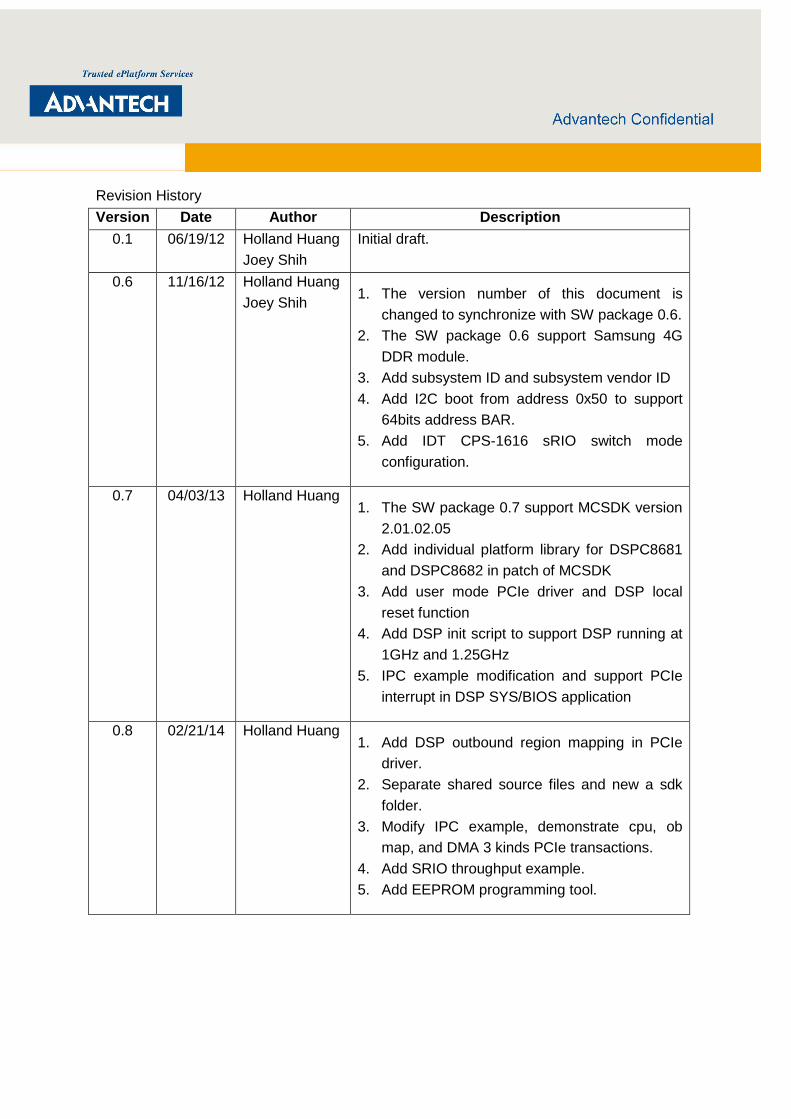
Revision History
Version Date Author Description
0.1 06/19/12 Holland Huang
Joey Shih
Initial draft.
0.6 11/16/12 Holland Huang
Joey Shih 1. The version number of this document is
changed to synchronize with SW package 0.6.
2. The SW package 0.6 support Samsung 4G
DDR module.
3. Add subsystem ID and subsystem vendor ID
4. Add I2C boot from address 0x50 to support
64bits address BAR.
5. Add IDT CPS-1616 sRIO switch mode
configuration.
0.7 04/03/13 Holland Huang 1. The SW package 0.7 support MCSDK version
2.01.02.05
2. Add individual platform library for DSPC8681
and DSPC8682 in patch of MCSDK
3. Add user mode PCIe driver and DSP local
reset function
4. Add DSP init script to support DSP running at
1GHz and 1.25GHz
5. IPC example modification and support PCIe
interrupt in DSP SYS/BIOS application
0.8 02/21/14 Holland Huang 1. Add DSP outbound region mapping in PCIe
driver.
2. Separate shared source files and new a sdk
folder.
3. Modify IPC example, demonstrate cpu, ob
map, and DMA 3 kinds PCIe transactions.
4. Add SRIO throughput example.
5. Add EEPROM programming tool.

Content
1. Introduction ................................................................................................................... 1
1.1. Hardware Description ........................................................................................ 1
1.2. DSPC-8682E Block Diagram ............................................................................. 1
1.3. DDR3 Interface .................................................................................................. 2
1.4. PCIe Interface .................................................................................................... 3
1.5. HyperLink Interface ............................................................................................ 3
1.6. Serial RapidIO Interface ..................................................................................... 3
1.7. SGMII Interface.................................................................................................. 4
1.8. DSP Identification .............................................................................................. 4
1.9. Hardware Environment Setting .......................................................................... 5
2. Package Content ........................................................................................................... 9
2.1. API Interface of DSP Driver ............................................................................... 9
2.2. DSP Program Loader Utility ............................................................................. 11
2.3. Example: DDR3 Initialization............................................................................ 11
2.4. Example: DSP Initialization for Local Reset ..................................................... 11
2.5. Example: Image Processing ............................................................................ 11
2.6. Example: IPC - PC/DSP Communication ......................................................... 12
2.7. Example: SRIO Throughput ............................................................................. 12
2.8. Example: Simple Web Server .......................................................................... 12
2.9. EEPROM Programming Tool ........................................................................... 12
2.10. Patch: Platform Library and NDK Library ......................................................... 12
3. DSP Program Loader .................................................................................................. 14
3.1. Host System Requirement ............................................................................... 14
3.2. Build Instruction ............................................................................................... 14
3.2.1. Build the Driver and Demo Application ................................................. 14
3.3. Installation and Usage ..................................................................................... 15
3.4. DSP Loader Utility ........................................................................................... 16
3.4.1. Query DSP Information ........................................................................ 17
3.4.2. Download DSP Program Image ........................................................... 18
3.4.3. DSP Memory Read .............................................................................. 18
3.4.4. DSP Memory Write............................................................................... 19
3.4.5. Download DSP Binary File ................................................................... 19
3.4.6. Save DSP Memory as a Binary File ..................................................... 20
3.4.7. DSP Local Reset .................................................................................. 20
4. Reference Implementations ......................................................................................... 22
4.1. Patch of Platform Library and NDK Library ...................................................... 22
4.1.1. How to Use Patch and Pre-built Libraries ............................................. 22
4.1.2. Build Instruction .................................................................................... 22
4.2. DSP DDR3 Initialization ................................................................................... 25
4.2.1. Build Instruction .................................................................................... 25
4.2.2. Usage .................................................................................................. 25
4.3. DSP Local Reset ............................................................................................. 26
4.3.1. Build Instruction .................................................................................... 26
4.3.2. Usage .................................................................................................. 27
4.4. Ethernet and Simple Web Server ..................................................................... 27
4.4.1. Build Instruction .................................................................................... 28
4.4.2. Usage .................................................................................................. 28
4.5. IPC Demo - Communication between PC and DSP ......................................... 30
4.5.1. Build Instruction .................................................................................... 31

4.5.2. Usage .................................................................................................. 31
4.5.3. PC Site Utility ....................................................................................... 40
4.5.4. DSP Demo Program ............................................................................. 40
4.6. Image Processing Demonstration .................................................................... 42
4.6.1. Build Instruction .................................................................................... 43
4.6.2. Usage .................................................................................................. 43
4.7. SRIO Throughput Benchmarking ..................................................................... 50
4.7.1. Build Instruction .................................................................................... 50
4.7.2. Usage .................................................................................................. 51
4.8. EEPROM Programming Tool ........................................................................... 54
4.8.1. Usage .................................................................................................. 54

1
1. Introduction
This document describes how to set up the software configurations for Octal-DSP PCIe board
(DSPC8682E), before using it. The DSPC8682E contains eight Texas Instruments
TMS320C6678 DSPs with PCIe, HyperLink, Serial RapidIO, and SGMII interfaces.
1.1. Hardware Description
The placement of the DSPC8682E is shown in Figure 1−1. Each board contains eight
TMS320C6678 (codename Shannon) DSPs, one PLX PEX8748 PCIe switch, and one Xilinx
XC3S200AN FPGA. The TMS320C6678 multi-core fixed and floating point digital signal
processor is based on advanced KeyStone architecture from Texas Instruments. Each
TMS320C6678 on DSPC8682E is supported by external DDR3 (the DDR3 module type
depends on different HW version) devices for data and program storage. The eight
TMS320C6678 devices are connected through PEX8748 PCIe device, which is 48-lane,
12-port PCIe Gen3 switch. The XC3S200AN FPGA device provides the required control
signals to the DSPC8682E.
Figure 1-1 DSPC-8682E Placement
1.2. DSPC-8682E Block Diagram
An interface block diagram for the DSPC8682E is shown in Figure 1−2. Each TMS320C6678
DSP contains several interfaces such as DDR, HyperLink, Serial RapidIO, and SGMII.

2
Figure 1-2 DSPC-8682E Interface Block Diagram
1.3. DDR3 Interface
Each TMS320C6678 DSP is connected to four 4Gbit DDR3 memory devices with 64-bit data
and 2GB capacity at current implementation. The DDR memory space is ranging from
0x80000000 to 0xFFFFFFFF at DSP device.
Note: The A101 version board is mounted 2Gbit DDR3 memory devices and 1GB capacity.
The DDR memory space of those boards will be ranging from 0x80000000 to 0xBFFFFFFF at
DSP device.
User can distinguish the HW version on DSPC-8682E backside: 19C2868200 is A101,
19C2868201-01 is A102.
Figure 1-3 Bar Code Label of DSPC-8682E
3
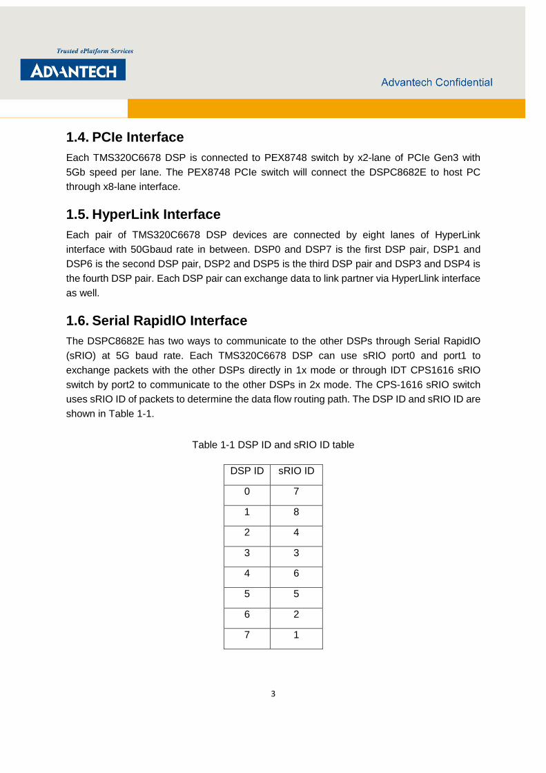
1.4. PCIe Interface
Each TMS320C6678 DSP is connected to PEX8748 switch by x2-lane of PCIe Gen3 with
5Gb speed per lane. The PEX8748 PCIe switch will connect the DSPC8682E to host PC
through x8-lane interface.
1.5. HyperLink Interface
Each pair of TMS320C6678 DSP devices are connected by eight lanes of HyperLink
interface with 50Gbaud rate in between. DSP0 and DSP7 is the first DSP pair, DSP1 and
DSP6 is the second DSP pair, DSP2 and DSP5 is the third DSP pair and DSP3 and DSP4 is
the fourth DSP pair. Each DSP pair can exchange data to link partner via HyperLlink interface
as well.
1.6. Serial RapidIO Interface
The DSPC8682E has two ways to communicate to the other DSPs through Serial RapidIO
(sRIO) at 5G baud rate. Each TMS320C6678 DSP can use sRIO port0 and port1 to
exchange packets with the other DSPs directly in 1x mode or through IDT CPS1616 sRIO
switch by port2 to communicate to the other DSPs in 2x mode. The CPS-1616 sRIO switch
uses sRIO ID of packets to determine the data flow routing path. The DSP ID and sRIO ID are
shown in Table 1-1.
Table 1-1 DSP ID and sRIO ID table
DSP ID sRIO ID
0 7
1 8
2 4
3 3
4 6
5 5
6 2
7 1

4
1.7. SGMII Interface
TMS320C6678 DSP contains an on-chip Ethernet switch with two Ethernet interfaces,
EMAC0 and EMAC1. TMS320C6678 DSP can connect to another DSP by Ethernet interface
without extra Ethernet switch in between. The SGMII interface connection and the topology of
the Ethernet link on the DSPC8682E is shown in Figure 1−2. The DSP0 on DSPC8682E
contains two SGMII interfaces and EMAC0 is connected to Broadcom BCM5482S Ethernet
PHY for external Ethernet access and EMAC1 is connected to EMAC0 of DSP1. EMAC1 of
DSP1 is connected to EMAC0 of DSP2. EMAC1 of DSP2 is connecting to EMAC0 of DSP3.
EMAC1 of DSP3 is connecting to EMAC0 of DSP4. EMAC1 of DSP4 is connecting to EMAC0
of DSP5. EMAC1 of DSP5 is connecting to EMAC0 of DSP6. The DSP7 EMAC1 is
connected to Broadcom BCM5482S Ethernet PHY for external Ethernet access and EMAC0
is connected to EMAC1 of DSP6. Programmers only need to enable Ethernet switch feature
of TMS320C6678 DSP and Ethernet packet will forward to the matched DSP by hardware
accelerator of on-chip Ethernet switch without intervention of DSP cores inside.
1.8. DSP Identification
The DSPC8682E use GPIO[1:3] pins to identify each DSP and the assignment of DSP ID is
shown below:
Table 1-2 DSP ID and GPIO table
GPIO 3 GPIO 2 GPIO 1
DSP 0 0 0 0
DSP 1 0 0 1
DSP 2 0 1 0
DSP 3 0 1 1
DSP 4 1 0 0
DSP 5 1 0 1
DSP 6 1 1 0
DSP 7 1 1 1
The Linux command “lspci” can list which type of board it is running by checking subsystem
ID and subsystem vendor ID as shown in Table 1-3.

5
Table 1-3 Subsystem ID and vendor ID table
SUBSYS_ID SUBSYS_VEN_ID
Value 0x8682 0x13FE
#lspci -vvnn -d:b005
04:00.0 Multimedia controller [0480]: Texas Instruments Device [104c:b005] (rev
01)
Subsystem: Advantech Co. Ltd Device [13fe:8682]
Control: I/O+ Mem+ BusMaster+ SpecCycle- MemWINV- VGASnoop- ParErr-
Stepping- SERR- FastB2B- DisINTx-
Status: Cap+ 66MHz- UDF- FastB2B- ParErr- DEVSEL=fast >TAbort- <TAbort-
<MAbort- >SERR- <PERR- INTx-
Latency: 0, Cache Line Size: 64 bytes
Interrupt: pin A routed to IRQ 11
Region 0: Memory at f8800000 (32-bit, non-prefetchable) [size=4K]
Region 1: Memory at df000000 (32-bit, prefetchable) [size=16M]
Region 2: Memory at de000000 (32-bit, prefetchable) [size=16M]
Region 3: Memory at dc000000 (32-bit, prefetchable) [size=32M]
Region 4: Memory at d8000000 (32-bit, prefetchable) [size=64M]
Capabilities: <access denied>
1.9. Hardware Environment Setting
The DSPC8682E supports two boot modes: Emulation mode and I2C mode. The user can
select boot mode by Switch-1 which is shown in Figure 1-4. The Emulation mode is mainly for
JTAG debug. The I2C boot mode is usually selected by Switch-1. DSPC-8682E includes
eight I2C EEPROMs to support the TMS320C6678 DSPs and each I2C EEPROM contains
program for 2-stage boot loader. The 2-stage boot loader will configure PLL and PCIE BAR
window when DSP boots up from I2C EEPROM. Table 1-4 shows the detailed configuration
of Switch-1.

6
Figure 1-4 I2C Boot Mode (PCIE boot) Setting
Table 1-4 Switch-1 Configuration Bit Field Description
Description
Switch Pins
Endian Boot Mode
1 2 3 4
Big-endian ON - - -
Little-endian (default) OFF - - -
Emulation boot mode - ON ON ON
I2C boot mode(Boot from address 0x51)
32bits address BAR setting (default) - OFF ON ON
I2C boot mode(Boot from address 0x50)
64bits address BAR setting - OFF OFF ON
Reserved - Others
The Figure 1-5 DIP switch is used to setup sRIO switch mode as below table.
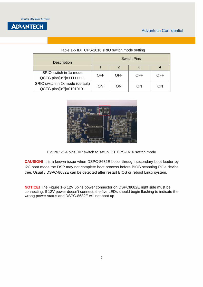
7
Table 1-5 IDT CPS-1616 sRIO switch mode setting
Description Switch Pins
1 2 3 4
SRIO switch in 1x mode
QCFG pins[0:7]=11111111 OFF OFF OFF OFF
SRIO switch in 2x mode (default)
QCFG pins[0:7]=01010101 ON ON ON ON
Figure 1-5 4 pins DIP switch to setup IDT CPS-1616 switch mode
CAUSION! It is a known issue when DSPC-8682E boots through secondary boot loader by
I2C boot mode the DSP may not complete boot process before BIOS scanning PCIe device
tree. Usually DSPC-8682E can be detected after restart BIOS or reboot Linux system.
NOTICE! The Figure 1-6 12V 6pins power connector on DSPC8682E right side must be connecting. If 12V power doesn’t connect, the five LEDs should begin flashing to indicate the wrong power status and DSPC-8682E will not boot up.

8
Figure 1-6 The 12V 6pins power connector
9
2. Package Content
This package is created to help customer quickly boot DSP through PCIE, the package
includes:
Table 2-1 Package content list
Path Purpose
Lightning_PCIE/dsp_loader/driver DSP Program Loader Driver
Lightning_PCIE/dsp_loader/app DSP Program Loader Utility
Lightning_PCIE/examples/ddr3 Example: DDR3 Initialization
Lightning_PCIE/examples/image_processing Example: Image Processing using Multi-Core
Lightning_PCIE/examples/ipc Example: IPC - PC/DSP Communication
Lightning_PCIE/examples/script Common demo related scripts
Lightning_PCIE/examples/ srio_throughput Example: SRIO Throughput Benchmarking
Lightning_PCIE/examples/web Example: Simple Web Server
Lightning_PCIE/tools/program_eeprom EEPROM programming tool
Lightning_PCIE/patch Patch: Platform Library and NDK Library of
PDK C6678 1.1.2.5 (inside MCSDK 2.1.2.5)
2.1. API Interface of DSP Driver
It is a Linux based PCIE driver which is used to map between PC memory and DSP memory.
A prerequisite for DMA to function is that memory needs to be contiguous in physical
memory. Memory allocated using malloc is not contiguous. Ubuntu Linux doesn’t have any
user mode APIs to allocate contiguous physical memory and hence a Kernel mode driver to
allocate contiguous physical memory is necessary. Currently, the implemented I/O controls
are listed below:
10
Table 2-2 Kernel Mode Driver I/O Control Code List
IOCTL code Description
TI667X_PCIEEP_IOCTL_GET_BAR_INFO Get the current BAR information of the
specified window
TI667x_PCIEEP_IOCTL_DMA_BUFFER_ALLOC Allocate buffers of contiguous in physical
memory for specified DSP
TI667x_PCIEEP_IOCTL_DMA_BUFFER_FREE Free all allocated buffers for specified DSP
TI667X_PCIEEP_IOCTL_GET_PCI_INFO Get PCI Information of DSP
A user mode driver is also provided. Developers can implement their own application based
on this user mode PCIe driver. The APIs are listed below:
Table 2-3 User Mode Driver API List
Export API Description
pcie_drv_open Open the devices which are registered by kernel driver, and
set up the access of PCIe BAR regions
pcie_drv_close Close the devices and free all allocated resources
pcie_drv_set_ep_config Set PCIe endpoint related configurations, such as interrupt
and privilege register.
pcie_drv_dsp_set_entry_point Write the entry point to boot magic address. The boot magic
address is the lasted DWORD of L2 memory, for C6678, the
address is 0x0087FFFC
pcie_drv_dsp_write Write to DSP memory using memcpy over PCIe
pcie_drv_dsp_read Read from DSP memory using memcpy over PCIe
pcie_drv_dma_mem_alloc Allocate contiguous host memory for specified DSP
pcie_drv_dma_mem_free Free the allocated physical memory and unmap all host
memory for specified DSP
pcie_drv_dma_write Write data to DSP memory from provided contiguous host
memory
pcie_drv_dma_read Read data from DSP memory to provided contiguous host
memory
11
pcie_drv_dsp_int_select Wait interrupt signal from DSP
pcie_drv_get_dsp_dev_info Get PCIe information of all DSP devices
2.2. DSP Program Loader Utility
DSP program loader utility is used to load .out files into DSPs and notify DSPs to run
program.
2.3. Example: DDR3 Initialization
The DDR3 initialization example contains CCS project settings to build a boot image. This
program will initialize DDR by reading parameter that stored in EEPROM(address 0x51,
offset 65500 bytes) after software 0.6 release, otherwise the Samsung 2Gb and Micron 4Gb
DDR module initialization parameter are hard code setting, DSP will wait loader utility to load
the next program after DDR initialization finished.
2.4. Example: DSP Initialization for Local Reset
The DSP reset example contains CCS project settings to build a boot image. This program is
a part of DSP local reset procedure. By running this program, core0 will poll PCIe legacy
INTA that is generated from host. Other cores will enter idle state after local reset related
registers are set by DSP Program Loader.
2.5. Example: Image Processing
The image processing demo example contains two CCS project settings to build the demo
images. This application will run TI image processing kernels (imagelib) on multiple cores to
do image processing (eg: edge detection, etc) on an input image. This program is modified
from TI MCSDK example which is located in the
mcsdk_2_01_02_05\demos\image_processing\ipc. The each DSP will be configured with a
static IP instead of DHCP.
12
2.6. Example: IPC - PC/DSP Communication
This example contains two parts, a DSP image and a PC utility. The dsp folder included
contains CCS project settings of building an image. This example provides sample codes on
how to communicate between PC and DSP.
2.7. Example: SRIO Throughput
The SRIO throughput example is created to allow user to run benchmarks with code that
utilizes the SRIO LLD APIs. This example provides two modes to allow for chip to chip with
SRIO switch connection and for chip to chip without SRIO switch connection.
2.8. Example: Simple Web Server
A web demo example contains CCS project settings to build an image. It can set up a web
server so user can use network browser to access the web page stored in the DSP. This
program is modified from TI MCSDK example which is located in the
mcsdk_2_01_02_05\examples\ndk\client. The each DSP will be configured with a static IP
instead of DHCP.
2.9. EEPROM Programming Tool
Lightning ver. 0.8 contains the EEPROM update firmware which is able to update BAR(Base
Address Register) from original 128MB to 32MB per DSP, to resolve the problem that PC
unable to boot which caused by insufficient memory.
2.10. Patch: Platform Library and NDK Library
There are some differences between the DSPC8682E and C6678 EVM, hence, developer
should patch these files in the TI PDK before using it. The modification is listed as below:
1. The DSPC8682E uses DSP0 EMAC0 and DSP7 EMAC1 to connect to BCM5482S
Ethernet PHY. This patch adds the initialization of SGMII port0 and change settings of
SGMII port 0 and port 1 for BCM5482S Ethernet PHY.
13
2. DSPC-8682E uses different DDR memory devices, the parameters for initialization of
DDR controller is not the same as C6678 EVM. This patch supports the DDR memory
device which is mounted on DSPC-8682E.
3. The reference clocks of DDR and SGMII is not the same as C6678 EVM and this patch
modifies the relevant MPY settings.

14
3. DSP Program Loader
After the whole system booting up, all DSP chips stay in idle mode. The PC is responsible to
download DSP codes to every chip and awaken DSPs to execute the loaded codes. The
loader consists of a driver and a utility running in PC Linux environment. This package
contains source code of the program loader. The developer must rebuild and install them to
the Linux before starting using the Lightning board.
3.1. Host System Requirement
A reference of the OS used to develop and execute this software release is:
1. Linux distribution: Ubuntu 10.10. Other distributions including Debian, Redhat, CentOS,
and Fedora should work with this software package.
2. Kernel: Linux kernel version 2.6.35.22. In fact, the driver should work with any kernel with
version >=2.6.20.
3. Pre-required Library: libreadline5-dev.deb or libreadline5-dev.rpm for Redhat families.
4. DSP development tool: TI Code Composer Studio v5.1 or higher, TI MCSDK for
TMS320C66x Processors V2.01.02.05, please refer to web site:
http://software-dl.ti.com/sdoemb/sdoemb_public_sw/bios_mcsdk/02_01_02_05/index_F
DS.html
3.2. Build Instruction
3.2.1. Build the Driver and Demo Application
The driver is closely tied to Linux kernel running on PC, therefore, it must be rebuilt to work
with the supporting kernel. The commands for building PCIE driver are listed below:
# /Lightning_PCIE/make clean
# /Lightning_PCIE/make
This compiles the PCIe kernel driver, user mode driver, dsp_loader utility and pc site
application of ipc example. The Module libraries can be found in the
dsp_loader/driver/module directory. The user mode driver library will be generated in the
dsp_loader/driver/lib directory. The dsp_loader executable can be found in
dsp_loader/app/bin directory. The pc site application dsp_demo executable will be produced
in the examples/ipc/pc/bin.
15
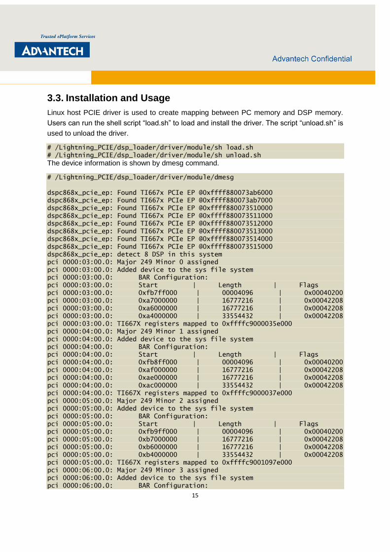
3.3. Installation and Usage
Linux host PCIE driver is used to create mapping between PC memory and DSP memory.
Users can run the shell script “load.sh” to load and install the driver. The script “unload.sh” is
used to unload the driver.
# /Lightning_PCIE/dsp_loader/driver/module/sh load.sh
# /Lightning_PCIE/dsp_loader/driver/module/sh unload.sh
The device information is shown by dmesg command.
# /Lightning_PCIE/dsp_loader/driver/module/dmesg
dspc868x_pcie_ep: Found TI667x PCIe EP @0xffff880073ab6000
dspc868x_pcie_ep: Found TI667x PCIe EP @0xffff880073ab7000
dspc868x_pcie_ep: Found TI667x PCIe EP @0xffff880073510000
dspc868x_pcie_ep: Found TI667x PCIe EP @0xffff880073511000
dspc868x_pcie_ep: Found TI667x PCIe EP @0xffff880073512000
dspc868x_pcie_ep: Found TI667x PCIe EP @0xffff880073513000
dspc868x_pcie_ep: Found TI667x PCIe EP @0xffff880073514000
dspc868x_pcie_ep: Found TI667x PCIe EP @0xffff880073515000
dspc868x_pcie_ep: detect 8 DSP in this system
pci 0000:03:00.0: Major 249 Minor 0 assigned
pci 0000:03:00.0: Added device to the sys file system
pci 0000:03:00.0: BAR Configuration:
pci 0000:03:00.0: Start | Length | Flags
pci 0000:03:00.0: 0xfb7ff000 | 00004096 | 0x00040200
pci 0000:03:00.0: 0xa7000000 | 16777216 | 0x00042208
pci 0000:03:00.0: 0xa6000000 | 16777216 | 0x00042208
pci 0000:03:00.0: 0xa4000000 | 33554432 | 0x00042208
pci 0000:03:00.0: TI667X registers mapped to 0xffffc9000035e000
pci 0000:04:00.0: Major 249 Minor 1 assigned
pci 0000:04:00.0: Added device to the sys file system
pci 0000:04:00.0: BAR Configuration:
pci 0000:04:00.0: Start | Length | Flags
pci 0000:04:00.0: 0xfb8ff000 | 00004096 | 0x00040200
pci 0000:04:00.0: 0xaf000000 | 16777216 | 0x00042208
pci 0000:04:00.0: 0xae000000 | 16777216 | 0x00042208
pci 0000:04:00.0: 0xac000000 | 33554432 | 0x00042208
pci 0000:04:00.0: TI667X registers mapped to 0xffffc9000037e000
pci 0000:05:00.0: Major 249 Minor 2 assigned
pci 0000:05:00.0: Added device to the sys file system
pci 0000:05:00.0: BAR Configuration:
pci 0000:05:00.0: Start | Length | Flags
pci 0000:05:00.0: 0xfb9ff000 | 00004096 | 0x00040200
pci 0000:05:00.0: 0xb7000000 | 16777216 | 0x00042208
pci 0000:05:00.0: 0xb6000000 | 16777216 | 0x00042208
pci 0000:05:00.0: 0xb4000000 | 33554432 | 0x00042208
pci 0000:05:00.0: TI667X registers mapped to 0xffffc9001097e000
pci 0000:06:00.0: Major 249 Minor 3 assigned
pci 0000:06:00.0: Added device to the sys file system
pci 0000:06:00.0: BAR Configuration:

16
pci 0000:06:00.0: Start | Length | Flags
pci 0000:06:00.0: 0xfbaff000 | 00004096 | 0x00040200
pci 0000:06:00.0: 0xbf000000 | 16777216 | 0x00042208
pci 0000:06:00.0: 0xbe000000 | 16777216 | 0x00042208
pci 0000:06:00.0: 0xbc000000 | 33554432 | 0x00042208
pci 0000:06:00.0: TI667X registers mapped to 0xffffc90010a16000
pci 0000:07:00.0: Major 249 Minor 4 assigned
pci 0000:07:00.0: Added device to the sys file system
pci 0000:07:00.0: BAR Configuration:
pci 0000:07:00.0: Start | Length | Flags
pci 0000:07:00.0: 0xfbbff000 | 00004096 | 0x00040200
pci 0000:07:00.0: 0xc7000000 | 16777216 | 0x00042208
pci 0000:07:00.0: 0xc6000000 | 16777216 | 0x00042208
pci 0000:07:00.0: 0xc4000000 | 33554432 | 0x00042208
pci 0000:07:00.0: TI667X registers mapped to 0xffffc90010a3e000
pci 0000:08:00.0: Major 249 Minor 5 assigned
pci 0000:08:00.0: Added device to the sys file system
pci 0000:08:00.0: BAR Configuration:
pci 0000:08:00.0: Start | Length | Flags
pci 0000:08:00.0: 0xfbcff000 | 00004096 | 0x00040200
pci 0000:08:00.0: 0xcf000000 | 16777216 | 0x00042208
pci 0000:08:00.0: 0xce000000 | 16777216 | 0x00042208
pci 0000:08:00.0: 0xcc000000 | 33554432 | 0x00042208
pci 0000:08:00.0: TI667X registers mapped to 0xffffc90010a7c000
pci 0000:09:00.0: Major 249 Minor 6 assigned
pci 0000:09:00.0: Added device to the sys file system
pci 0000:09:00.0: BAR Configuration:
pci 0000:09:00.0: Start | Length | Flags
pci 0000:09:00.0: 0xfbdff000 | 00004096 | 0x00040200
pci 0000:09:00.0: 0xd7000000 | 16777216 | 0x00042208
pci 0000:09:00.0: 0xd6000000 | 16777216 | 0x00042208
pci 0000:09:00.0: 0xd4000000 | 33554432 | 0x00042208
pci 0000:09:00.0: TI667X registers mapped to 0xffffc90010a7e000
pci 0000:0a:00.0: Major 249 Minor 7 assigned
pci 0000:0a:00.0: Added device to the sys file system
pci 0000:0a:00.0: BAR Configuration:
pci 0000:0a:00.0: Start | Length | Flags
pci 0000:0a:00.0: 0xfbeff000 | 00004096 | 0x00040200
pci 0000:0a:00.0: 0xdf000000 | 16777216 | 0x00042208
pci 0000:0a:00.0: 0xde000000 | 16777216 | 0x00042208
pci 0000:0a:00.0: 0xdc000000 | 33554432 | 0x00042208
pci 0000:0a:00.0: TI667X registers mapped to 0xffffc90010e92000
3.4. DSP Loader Utility
DSP loader offers the functions to load the program into DSP memory and notify the DSP to
run program.
17
3.4.1. Query DSP Information
The command syntax is:
dsp_loader query list or dsp_loader query -l
dsp_loader query [chip#]
The command is to display the PCI information of DSP which are installed in the system. The
more detailed information will be displayed when user specify the [chip#] parameter. The
[chip#] are the number of DSPs attached to the PC. Since there are eight DSP devices on the
DSPC8682E, this parameter can be set into 0 ~ 7 for those PC systems installed with one
DSPC8682E card. For those PC systems installed with two DSPC8682E cards, there will be
sixteen chips available to the PC systems and the parameter can be set into 0 ~ 15.
The following two examples demonstrate the result of query command when PC system
install DSPC8682E card and query the detailed information of DSP#7.
# /Lightning_PCIE/dsp_loader/app/bin/dsp_loader query list
Card 0:
[Chip 0] Device 8682
[Chip 1] Device 8682
[Chip 2] Device 8682
[Chip 3] Device 8682
[Chip 4] Device 8682
[Chip 5] Device 8682
[Chip 6] Device 8682
[Chip 7] Device 8682
# /Lightning_PCIE/dsp_loader/app/bin/dsp_loader query 7
==============================================
Chip: 7
PCI Bridge 2
PCI Bus Num: 10
Vendor ID: 0x104c Device ID: 0xb005
Subsystem VendorID: 0x13fe Subsystem DevID: 0x8682
Class: 0x00048000
Header Type: 0 Irq Pin: 1
BAR Configuration:
Start | Length | Flags
0xfbeff000 | 00004096 | 0x00020200
0xdf000000 | 16777216 | 0x00021208
0xde000000 | 16777216 | 0x00021208
0xdc000000 | 33554432 | 0x00021208
==============================================
18
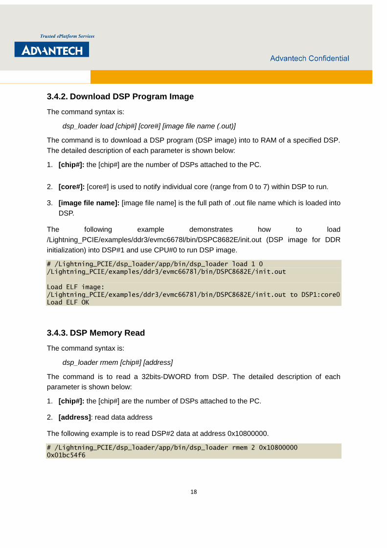
3.4.2. Download DSP Program Image
The command syntax is:
dsp_loader load [chip#] [core#] [image file name (.out)]
The command is to download a DSP program (DSP image) into to RAM of a specified DSP.
The detailed description of each parameter is shown below:
1. [chip#]: the [chip#] are the number of DSPs attached to the PC.
2. [core#]: [core#] is used to notify individual core (range from 0 to 7) within DSP to run.
3. [image file name]: [image file name] is the full path of .out file name which is loaded into
DSP.
The following example demonstrates how to load
/Lightning_PCIE/examples/ddr3/evmc6678l/bin/DSPC8682E/init.out (DSP image for DDR
initialization) into DSP#1 and use CPU#0 to run DSP image.
# /Lightning_PCIE/dsp_loader/app/bin/dsp_loader load 1 0
/Lightning_PCIE/examples/ddr3/evmc6678l/bin/DSPC8682E/init.out
Load ELF image:
/Lightning_PCIE/examples/ddr3/evmc6678l/bin/DSPC8682E/init.out to DSP1:core0
Load ELF OK
3.4.3. DSP Memory Read
The command syntax is:
dsp_loader rmem [chip#] [address]
The command is to read a 32bits-DWORD from DSP. The detailed description of each
parameter is shown below:
1. [chip#]: the [chip#] are the number of DSPs attached to the PC.
2. [address]: read data address
The following example is to read DSP#2 data at address 0x10800000.
# /Lightning_PCIE/dsp_loader/app/bin/dsp_loader rmem 2 0x10800000
0x01bc54f6

19
3.4.4. DSP Memory Write
The command syntax is:
dsp_loader wmem [chip#] [address] [value]
The command is to write a 32bits-DWORD into DSP memory. The detailed description of
each parameter is shown below:
1. [chip#]: the [chip#] are the number of DSPs attached to the PC.
2. [address]: written data address
3. [value]: written data
The following example writes data 0x55AA55AA into DSP#2 at address 0x10800000.
# /Lightning_PCIE/dsp_loader/app/bin/dsp_loader wmem 2 0x10800000 0x55aa55aa
# /Lightning_PCIE/dsp_loader/app/bin/dsp_loader rmem 2 0x10800000
0x55aa55aa
3.4.5. Download DSP Binary File
The command syntax is:
dsp_loader loadbinary [chip#] [address] [size] [transfer type] [bin file name]
The command is to write a bin file into DSP memory. The detailed description of each
parameter is shown below:
1. [chip#]: the [chip#] are the number of DSPs attached to the PC.
2. [address]: written data address
3. [size]: written data size, 0 for all data of file.
4. [transfer type]: 0 for CPU memcpy, 1 for DMA.
5. [bin file name]: [bin file name] is the full path of binary file name which is loaded into
DSP.
The following example writes a jpg file into DSP#1 at DDR beginning address 0x80000000 by
using DMA.
# /Lightning_PCIE/dsp_loader/app/bin/dsp_loader loadbinary 1 0x80000000 0 1
/home/advantech/test_image.jpg
Load Binary file: /home/advantech/test_image.jpg to DSP1, start address
0x80000000, Size 0x00000000
Written to dsp 7496169 bytes
Time measured: 16225 us
20
Load Binary OK
3.4.6. Save DSP Memory as a Binary File
The command syntax is:
dsp_loader savebinary [chip#] [address] [size] [transfer type] [bin file name]
The command is to read a DSP memory section and save the data as a binary file. The
detailed description of each parameter is shown below:
1. [chip#]: the [chip#] are the number of DSPs attached to the PC.
2. [address]: read data address
3. [size]: read data size
4. [transfer type]: 0 for CPU memcpy, 1 for DMA.
5. [bin file name]: [bin file name] is the full path of binary file name which is saved.
The following example read 7496169 bytes from DSP#1 at DDR beginning address
0x80000000 by using DMA, and saves as test_image_output.jpg.
# /Lightning_PCIE/dsp_loader/app/bin/dsp_loader loadbinary 1 0x80000000 0 1
/home/advantech/test_image.jpg
Load Binary file: /home/advantech/test_image.jpg to DSP1, start address
0x80000000, Size 0x00000000
Written to dsp 7496169 bytes
Time measured: 16225 us
Load Binary OK
# /Lightning_PCIE/dsp_loader/app/bin/dsp_loader savebinary 1 0x80000000 7496169
1 /home/advantech/test_image_output.jpg
Save Binary file: /home/advantech/test_image_output.jpg from DSP 1, start
address 0x80000000 Size 0x007261e9
Saved from dsp 7496169 bytes
Time measured: 21871 us
Save Binary OK
3.4.7. DSP Local Reset
The command syntax is:
dsp_loader reset [chip#]
The command is to do a local reset of DSP. The detailed description of each parameter is
shown below:
1. [chip#]: the [chip#] are the number of DSPs attached to the PC.
21
The following example reset DSP#0.
# /Lightning_PCIE/dsp_loader/app/bin/dsp_loader reset 0
Iterations waited for entry point to clear 1
Dsp 0: DSP Reset success !
22
4. Reference Implementations
4.1. Patch of Platform Library and NDK Library
The example programs have to link with DSPC8682 platform library and NDK library. A
developer has to install MCSDK first and applies the provided patch. The default path of
MCSDK in Windows is "C:\Program Files\Texas Instruments\" or "C:\ti".
4.1.1. How to Use Patch and Pre-built Libraries
1. Copy Lightning_PCIE\patch\pdk_C6678_1_1_2_5.
2. Paste to C:\Program Files\Texas Instruments\pdk_C6678_1_1_2_5.
3. The pre-built libraries are included in the provided patch, a developer can use these
libraries directly.
4.1.2. Build Instruction
Steps to build platform lib are listed below:
1. Import the CCS project from
"pdk_C6678_1_1_2_5\packages\ti\platform\dspc8682\platform_lib" directory (in CCSv5,
Project->Import Existing CCS/CCE Eclipse Projects)
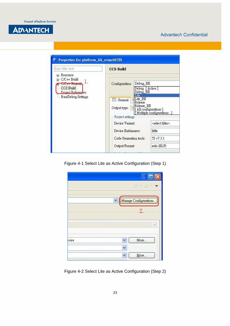
2. Refer to Figure 4-1 ~ Figure 4-3 and select "Lite" as active configuration (in CCSv5,
Project->Properties)
23
Figure 4-1 Select Lite as Active Configuration (Step 1)
Figure 4-2 Select Lite as Active Configuration (Step 2)

24
Figure 4-3 Select Lite as Active Configuration (Step 2)
3. Clean the platform_lib_dspc8682 project and re-build the project. After build is completed
the ti.platform.dspc8682.lite.lib will be generated under the directory:
"pdk_C6678_1_1_2_5\packages\ti\platform\dspc8682\platform_lib\lib\debug"
4. Repeat step 2 and step 3, select "Debug" as active configuration and re-build the project.
ti.platform.dspc8682.ae66 will be generated under the same directory
Steps to build ndk lib are listed below:
1. Import the CCS project from "pdk_C6678_1_1_2_5\packages\ti\transport\ndk\nimu"
directory (in CCSv5, Project->Import Existing CCS/CCE Eclipse Projects)
2. Clean the nimu_eth_evmc6678l project and re-build the project. After build is completed,
ti.transport.ndk.nimu.ae66 will be generated under the directory:
"pdk_C6678_1_1_2_5\packages\ti\transport\ndk\nimu\lib\debug"
25
4.2. DSP DDR3 Initialization
The Boot ROM codes only initialize L2 internal memory when booting from PCIE boot mode.
The on-board DDR3 control registers need to be explicitly initialized by this supplied example
program. User has to initialize DDR3 control registers before loading the application into
DSP. After initialization of DDR3 control registers, this program will clear boot address and
wait dsp_loader to write new entry point in boot address. When boot address is updated, this
program will jump to new entry point and start to run the next program.
4.2.1. Build Instruction
Steps to build DDR3 initialization program are listed below:
1. Import the demo_evmc6678l_init CCS project from
"Lightning_PCIE\examples\ddr3\evmc6678l" directory (in CCSv5, Project->Import
Existing CCS/ CCE Eclipse Projects)
2. Select DSPC8682E as active configuration
3. Clean the demo_evmc6678l_init project and re-build the project. After build is completed,
init.out and init.map will be generated under
"Lightning_PCIE\examples\ddr3\evmc6678l\bin\DSPC8682E" directory
4.2.2. Usage
User can use the shell script examples\script\DSPC8682E\init_1000.sh or init_1250.sh to
initialize DSP DDR, the procedure is composed of two jobs,
1. Externally set PLL Multiplier configuration (by dsp_loader)
2. Load .out file to DSP (by dsp_loader)
There are two scripts, init_1000.sh and init_1250.sh for users to initialize DSP. They load the
init.out in Lightning_PCIE\examples\ddr3\evmc6678l\bin. DSP initialization can be done by
invoking the init scripts. The difference between init_1000.sh and init_1250.sh is that the
former runs DSP at 1GHz, the latter overclocks DSP to 1.25GHz. There is the prebuilt binary
bundled in Lightning_PCIE\examples\ddr3\evmc6678l\bin. Users can initialize DSP DDR
module without building the image from source. However, when running the script, it will show
the version of your DSP (PG1 or PG2), and for PG2 chip, it will also show the maximum
running frequency, e.g., 1GHz, 1.2GHz, or 1.25GHz.
Notice: At present, we only guarantee the stability for PG2 version of C6678 to run at 1GHz.
The following example initializes 8 DSP.

26
# /Lightning_PCIE/examples/script/DSPC8682E/init_1000.sh 8
DSP type: silicon Version = PG2.0, DSP maximum frequency limit = 1GHz
Load ELF image: ../../../examples/ddr3/evmc6678l/bin/DSPC8682E/init.out to
DSP0:core0
Load ELF OK
DSP type: silicon Version = PG2.0, DSP maximum frequency limit = 1GHz
Load ELF image: ../../../examples/ddr3/evmc6678l/bin/DSPC8682E/init.out to
DSP1:core0
Load ELF OK
DSP type: silicon Version = PG2.0, DSP maximum frequency limit = 1GHz
Load ELF image: ../../../examples/ddr3/evmc6678l/bin/DSPC8682E/init.out to
DSP2:core0
Load ELF OK
DSP type: silicon Version = PG2.0, DSP maximum frequency limit = 1GHz
Load ELF image: ../../../examples/ddr3/evmc6678l/bin/DSPC8682E/init.out to
DSP3:core0
Load ELF OK
DSP type: silicon Version = PG2.0, DSP maximum frequency limit = 1GHz
Load ELF image: ../../../examples/ddr3/evmc6678l/bin/DSPC8682E/init.out to
DSP4:core0
Load ELF OK
DSP type: silicon Version = PG2.0, DSP maximum frequency limit = 1GHz
Load ELF image: ../../../examples/ddr3/evmc6678l/bin/DSPC8682E/init.out to
DSP5:core0
Load ELF OK
DSP type: silicon Version = PG2.0, DSP maximum frequency limit = 1GHz
Load ELF image: ../../../examples/ddr3/evmc6678l/bin/DSPC8682E/init.out to
DSP6:core0
Load ELF OK
DSP type: silicon Version = PG2.0, DSP maximum frequency limit = 1GHz
Load ELF image: ../../../examples/ddr3/evmc6678l/bin/DSPC8682E/init.out to
DSP7:core0
Load ELF OK
4.3. DSP Local Reset
After DSP code is downloaded once, the DSP runs downloaded code. In order to
re-download the different DSP code, the DSP local reset function is needed. When user
perform the reset function by DSP loader utility, the utility will configure related registers of
each module of DSP, and download the DSP reset program to each core. The file format
conversion tool is also included and can be used to convert .out file format into .h file, which
will be used as the source file when make DSP loader utility.
4.3.1. Build Instruction
Steps to build DSP reset program are listed below:
27
1. Import the pcieboot_localreset CCS project from
"Lightning_PCIE\sdk\dspreset\c66x\build" directory (in CCSv5, Project->Import Existing
CCS/ CCE Eclipse Projects)
2. Clean the pcieboot_localreset project and re-build the project. After build is completed,
pcieboot_localreset.out and pcieboot_localreset.map will be generated under
"Lightning_PCIE\sdk\dspreset\c66x\build\bin" directory
3. Enter in "Lightning_PCIE\sdk\dspreset\utils\elf2HUtils" and launch
pcieboot_localreset_elf2HBin.sh, After the steps of script are completed, the
pcieLocalReset.h will be generated under "Lightning_PCIE\sdk\dsploader\host\inc"
4. Enter in "Lightning_PCIE\", make clean and make (follow chap 3.2) to re-build DSP
loader.
4.3.2. Usage
Refer to 3.4.7 to get detailed procedure of the DSP local reset.
4.4. Ethernet and Simple Web Server
The Ethernet program is modified from the example codes in TI MCSDK. This example
implements a simple web server running on DSP. The Ethernet port on the bracket of the
DSPC8682E must be connected to an external Ethernet switch (support gigabit rate) before
running this example. Each DSP has a fixed IP number that is determined by its order. The
pre-given IP addresses are shown below. The user can use a browser to view the simple web
page provided by this simple web server.
Table 4-1 DSP IP address table
IP
DSP 0 192.168.1.101
DSP 1 192.168.1.102
DSP 2 192.168.1.103
DSP 3 192.168.1.104
DSP 4 192.168.1.105
DSP 5 192.168.1.106

28
DSP 6 192.168.1.107
DSP 7 192.168.1.108
4.4.1. Build Instruction
Steps to build web server program are listed below:
1. Import the client_evmc6678l CCS project from
"Lightning_PCIE\examples\web\client\evmc6678l" directory (in CCSv5, Project->Import
Existing CCS/ CCE Eclipse Projects)
2. Select DSPC8682E as active configuration.
3. Clean the client_evmc6678l project and re-build the project. After build is completed,
client_evmc6678l.out and client_evmc6678l.map will be generated under
"Lightning_PCIE\examples\web\client\evmc6678l\DSPC8682E" directory
4.4.2. Usage
User can use the shell script "Lightning_PCIE/examples/script/DSPC8682E/web/ethernet.sh"
to setup Ethernet program on each DSP automatically. The following steps set up ethernet
program on 8 DSPs.
1. Perform the init_1000.sh to initialize DDR
2. Perform the ethernet.sh to load client_evmc6678l.out file into each DSP.
# /Lightning_PCIE/examples/script/DSPC8682E/web/ethetnet.sh 8
Load ELF image: ../../../bin/DSPC8682E/client_evmc6678l.out to DSP0:core0
Load ELF OK
Load ELF image: ../../../bin/DSPC8682E/client_evmc6678l.out to DSP1:core0
Load ELF OK
Load ELF image: ../../../bin/DSPC8682E/client_evmc6678l.out to DSP2:core0
Load ELF OK
Load ELF image: ../../../bin/DSPC8682E/client_evmc6678l.out to DSP3:core0
Load ELF OK
Load ELF image: ../../../bin/DSPC8682E/client_evmc6678l.out to DSP4:core0
Load ELF OK
Load ELF image: ../../../bin/DSPC8682E/client_evmc6678l.out to DSP5:core0
Load ELF OK
Load ELF image: ../../../bin/DSPC8682E/client_evmc6678l.out to DSP6:core0
Load ELF OK
Load ELF image: ../../../bin/DSPC8682E/client_evmc6678l.out to DSP7:core0
Load ELF OK
29
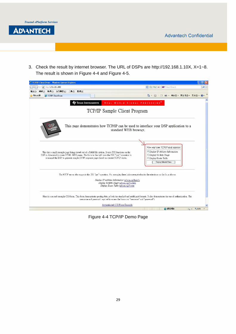
3. Check the result by internet browser. The URL of DSPs are http://192.168.1.10X, X=1~8.
The result is shown in Figure 4-4 and Figure 4-5.
Figure 4-4 TCP/IP Demo Page

30
Figure 4-5 IP Address Information page
4.5. IPC Demo - Communication between PC and DSP
This example demonstrates several functions for manipulating the DSPs including:
1. Write data blocks to DSP memory from PC
2. Read back data blocks from DSP memory to PC
3. PC interrupts DSP
4. DSP interrupts PC

31
4.5.1. Build Instruction
Steps to build ipc DSP program are listed below:
1. Import the dspc868x_demo CCS project from
"Lightning_PCIE\examples\ipc\dsp\dspc868x" directory (in CCSv5, Project->Import
Existing CCS/ CCE Eclipse Projects)
2. Select DSPC8682E as active configuration.
3. Clean the dspc868x_demo project and re-build the project. After build is completed,
demo_dspc868x.out and demo_dspc868x.map will be generated under
"Lightning_PCIE\examples\ipc\dsp\dspc868x\bin\DSPC8682E" directory
4.5.2. Usage
User can use shell script file "Lightning_PCIE/examples/script/DSPC8682E/ipc/load_ipc.sh"
to load demo_dspc868x.out into the specific DSP. The script will do following two jobs.
1. Load DSP stress test code to the specified DSP for core 1 to core 7
2. Load DSP ethernet code for core 0
There are four steps to launch IPC example,
1. Perform init_1000.sh to initialize DDR
2. Enter ipc folder and prepare a binary file renamed test.file, which is used as the input file
Note: Remember to use an appropriately sized file for this test. The size of the file is
recommended to be > 2 * Number of DSP * PAYLOAD_SIZE( e.g When using a octal DSP
card and using a payload size input during 4 MB, the minimum file size to be used is
recommended to be >64 MBytes (2 * 8 DSPs * 4 MB ), so that all the DSPs in the card are
used in the test at least twice.
3. Run load_ipc.sh to load demo_dspc868x.out into the specific DSP
# /Lightning_PCIE/examples/script/DSPC8682E/ipc/load_ipc.sh 8
==========================================
Loading DSP stress test code for core1~core7...
Load ELF
image: ../../../examples/ipc/dsp/dspc868x/bin/DSPC8682E/demo_dspc868x.out to
DSP0:core1
Load ELF OK

32
Load ELF
image: ../../../examples/ipc/dsp/dspc868x/bin/DSPC8682E/demo_dspc868x.out to
DSP0:core2
Load ELF OK
Load ELF
image: ../../../examples/ipc/dsp/dspc868x/bin/DSPC8682E/demo_dspc868x.out to
DSP0:core3
Load ELF OK
Load ELF
image: ../../../examples/ipc/dsp/dspc868x/bin/DSPC8682E/demo_dspc868x.out to
DSP0:core4
Load ELF OK
Load ELF
image: ../../../examples/ipc/dsp/dspc868x/bin/DSPC8682E/demo_dspc868x.out to
DSP0:core5
Load ELF OK
Load ELF
image: ../../../examples/ipc/dsp/dspc868x/bin/DSPC8682E/demo_dspc868x.out to
DSP0:core6
Load ELF OK
Load ELF
image: ../../../examples/ipc/dsp/dspc868x/bin/DSPC8682E/demo_dspc868x.out to
DSP0:core7
Load ELF OK
Load ELF
image: ../../../examples/ipc/dsp/dspc868x/bin/DSPC8682E/demo_dspc868x.out to
DSP1:core1
Load ELF OK
Load ELF
image: ../../../examples/ipc/dsp/dspc868x/bin/DSPC8682E/demo_dspc868x.out to
DSP1:core2
Load ELF OK
Load ELF
image: ../../../examples/ipc/dsp/dspc868x/bin/DSPC8682E/demo_dspc868x.out to
DSP1:core3
Load ELF OK
Load ELF
image: ../../../examples/ipc/dsp/dspc868x/bin/DSPC8682E/demo_dspc868x.out to
DSP1:core4
Load ELF OK
Load ELF
image: ../../../examples/ipc/dsp/dspc868x/bin/DSPC8682E/demo_dspc868x.out to
DSP1:core5
Load ELF OK
Load ELF
image: ../../../examples/ipc/dsp/dspc868x/bin/DSPC8682E/demo_dspc868x.out to
DSP1:core6
Load ELF OK
Load ELF
image: ../../../examples/ipc/dsp/dspc868x/bin/DSPC8682E/demo_dspc868x.out to
DSP1:core7

33
Load ELF OK
Load ELF
image: ../../../examples/ipc/dsp/dspc868x/bin/DSPC8682E/demo_dspc868x.out to
DSP2:core1
Load ELF OK
Load ELF
image: ../../../examples/ipc/dsp/dspc868x/bin/DSPC8682E/demo_dspc868x.out to
DSP2:core2
Load ELF OK
Load ELF
image: ../../../examples/ipc/dsp/dspc868x/bin/DSPC8682E/demo_dspc868x.out to
DSP2:core3
Load ELF OK
Load ELF
image: ../../../examples/ipc/dsp/dspc868x/bin/DSPC8682E/demo_dspc868x.out to
DSP2:core4
Load ELF OK
Load ELF
image: ../../../examples/ipc/dsp/dspc868x/bin/DSPC8682E/demo_dspc868x.out to
DSP2:core5
Load ELF OK
Load ELF
image: ../../../examples/ipc/dsp/dspc868x/bin/DSPC8682E/demo_dspc868x.out to
DSP2:core6
Load ELF OK
Load ELF
image: ../../../examples/ipc/dsp/dspc868x/bin/DSPC8682E/demo_dspc868x.out to
DSP2:core7
Load ELF OK
Load ELF
image: ../../../examples/ipc/dsp/dspc868x/bin/DSPC8682E/demo_dspc868x.out to
DSP3:core1
Load ELF OK
Load ELF
image: ../../../examples/ipc/dsp/dspc868x/bin/DSPC8682E/demo_dspc868x.out to
DSP3:core2
Load ELF OK
Load ELF
image: ../../../examples/ipc/dsp/dspc868x/bin/DSPC8682E/demo_dspc868x.out to
DSP3:core3
Load ELF OK
Load ELF
image: ../../../examples/ipc/dsp/dspc868x/bin/DSPC8682E/demo_dspc868x.out to
DSP3:core4
Load ELF OK
Load ELF
image: ../../../examples/ipc/dsp/dspc868x/bin/DSPC8682E/demo_dspc868x.out to
DSP3:core5
Load ELF OK
Load ELF
image: ../../../examples/ipc/dsp/dspc868x/bin/DSPC8682E/demo_dspc868x.out to
34
DSP3:core6
Load ELF OK
Load ELF
image: ../../../examples/ipc/dsp/dspc868x/bin/DSPC8682E/demo_dspc868x.out to
DSP3:core7
Load ELF OK
Load ELF
image: ../../../examples/ipc/dsp/dspc868x/bin/DSPC8682E/demo_dspc868x.out to
DSP4:core1
Load ELF OK
Load ELF
image: ../../../examples/ipc/dsp/dspc868x/bin/DSPC8682E/demo_dspc868x.out to
DSP4:core2
Load ELF OK
Load ELF
image: ../../../examples/ipc/dsp/dspc868x/bin/DSPC8682E/demo_dspc868x.out to
DSP4:core3
Load ELF OK
Load ELF
image: ../../../examples/ipc/dsp/dspc868x/bin/DSPC8682E/demo_dspc868x.out to
DSP4:core4
Load ELF OK
Load ELF
image: ../../../examples/ipc/dsp/dspc868x/bin/DSPC8682E/demo_dspc868x.out to
DSP4:core5
Load ELF OK
Load ELF
image: ../../../examples/ipc/dsp/dspc868x/bin/DSPC8682E/demo_dspc868x.out to
DSP4:core6
Load ELF OK
Load ELF
image: ../../../examples/ipc/dsp/dspc868x/bin/DSPC8682E/demo_dspc868x.out to
DSP4:core7
Load ELF OK
Load ELF
image: ../../../examples/ipc/dsp/dspc868x/bin/DSPC8682E/demo_dspc868x.out to
DSP5:core1
Load ELF OK
Load ELF
image: ../../../examples/ipc/dsp/dspc868x/bin/DSPC8682E/demo_dspc868x.out to
DSP5:core2
Load ELF OK
Load ELF
image: ../../../examples/ipc/dsp/dspc868x/bin/DSPC8682E/demo_dspc868x.out to
DSP5:core3
Load ELF OK
Load ELF
image: ../../../examples/ipc/dsp/dspc868x/bin/DSPC8682E/demo_dspc868x.out to
DSP5:core4
Load ELF OK
Load ELF

35
image: ../../../examples/ipc/dsp/dspc868x/bin/DSPC8682E/demo_dspc868x.out to
DSP5:core5
Load ELF OK
Load ELF
image: ../../../examples/ipc/dsp/dspc868x/bin/DSPC8682E/demo_dspc868x.out to
DSP5:core6
Load ELF OK
Load ELF
image: ../../../examples/ipc/dsp/dspc868x/bin/DSPC8682E/demo_dspc868x.out to
DSP5:core7
Load ELF OK
Load ELF
image: ../../../examples/ipc/dsp/dspc868x/bin/DSPC8682E/demo_dspc868x.out to
DSP6:core1
Load ELF OK
Load ELF
image: ../../../examples/ipc/dsp/dspc868x/bin/DSPC8682E/demo_dspc868x.out to
DSP6:core2
Load ELF OK
Load ELF
image: ../../../examples/ipc/dsp/dspc868x/bin/DSPC8682E/demo_dspc868x.out to
DSP6:core3
Load ELF OK
Load ELF
image: ../../../examples/ipc/dsp/dspc868x/bin/DSPC8682E/demo_dspc868x.out to
DSP6:core4
Load ELF OK
Load ELF
image: ../../../examples/ipc/dsp/dspc868x/bin/DSPC8682E/demo_dspc868x.out to
DSP6:core5
Load ELF OK
Load ELF
image: ../../../examples/ipc/dsp/dspc868x/bin/DSPC8682E/demo_dspc868x.out to
DSP6:core6
Load ELF OK
Load ELF
image: ../../../examples/ipc/dsp/dspc868x/bin/DSPC8682E/demo_dspc868x.out to
DSP6:core7
Load ELF OK
Load ELF
image: ../../../examples/ipc/dsp/dspc868x/bin/DSPC8682E/demo_dspc868x.out to
DSP7:core1
Load ELF OK
Load ELF
image: ../../../examples/ipc/dsp/dspc868x/bin/DSPC8682E/demo_dspc868x.out to
DSP7:core2
Load ELF OK
Load ELF
image: ../../../examples/ipc/dsp/dspc868x/bin/DSPC8682E/demo_dspc868x.out to
DSP7:core3
Load ELF OK

36
Load ELF
image: ../../../examples/ipc/dsp/dspc868x/bin/DSPC8682E/demo_dspc868x.out to
DSP7:core4
Load ELF OK
Load ELF
image: ../../../examples/ipc/dsp/dspc868x/bin/DSPC8682E/demo_dspc868x.out to
DSP7:core5
Load ELF OK
Load ELF
image: ../../../examples/ipc/dsp/dspc868x/bin/DSPC8682E/demo_dspc868x.out to
DSP7:core6
Load ELF OK
Load ELF
image: ../../../examples/ipc/dsp/dspc868x/bin/DSPC8682E/demo_dspc868x.out to
DSP7:core7
Load ELF OK
==========================================
Loading DSP ethernet code for core0...
Load ELF
image: ../../../examples/ipc/dsp/dspc868x/bin/DSPC8682E/demo_dspc868x.out to
DSP0:core0
Load ELF OK
Load ELF
image: ../../../examples/ipc/dsp/dspc868x/bin/DSPC8682E/demo_dspc868x.out to
DSP1:core0
Load ELF OK
Load ELF
image: ../../../examples/ipc/dsp/dspc868x/bin/DSPC8682E/demo_dspc868x.out to
DSP2:core0
Load ELF OK
Load ELF
image: ../../../examples/ipc/dsp/dspc868x/bin/DSPC8682E/demo_dspc868x.out to
DSP3:core0
Load ELF OK
Load ELF
image: ../../../examples/ipc/dsp/dspc868x/bin/DSPC8682E/demo_dspc868x.out to
DSP4:core0
Load ELF OK
Load ELF
image: ../../../examples/ipc/dsp/dspc868x/bin/DSPC8682E/demo_dspc868x.out to
DSP5:core0
Load ELF OK
Load ELF
image: ../../../examples/ipc/dsp/dspc868x/bin/DSPC8682E/demo_dspc868x.out to
DSP6:core0
Load ELF OK
Load ELF
image: ../../../examples/ipc/dsp/dspc868x/bin/DSPC8682E/demo_dspc868x.out to
DSP7:core0
Load ELF OK

37
4. Run any of the following to run the test, based on the data transfer mode to be used in the
test
a) Data transfer using CPU
b) Data transfer using DMA
c) Data transfer using Out-of-Band mapping
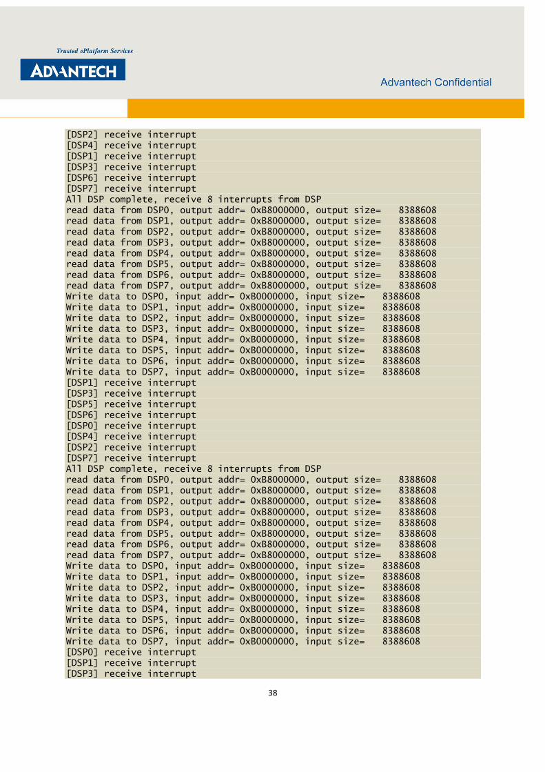
The following example captures the result of running "
Lightning_PCIE/examples/script/DSPC8682E/ipc/run_ipc_dma.sh ". The size of test.file is
322249961 bytes. The output file “test.file.out” is generated by the test, and console shows
the result of file comparison.
# /Lightning_PCIE/examples/script/DSPC8682E/ipc/run_ipc_dma.sh 8
Write data to DSP0, input addr= 0xB0000000, input size= 8388608
Write data to DSP1, input addr= 0xB0000000, input size= 8388608
Write data to DSP2, input addr= 0xB0000000, input size= 8388608
Write data to DSP3, input addr= 0xB0000000, input size= 8388608
Write data to DSP4, input addr= 0xB0000000, input size= 8388608
Write data to DSP5, input addr= 0xB0000000, input size= 8388608
Write data to DSP6, input addr= 0xB0000000, input size= 8388608
Write data to DSP7, input addr= 0xB0000000, input size= 8388608
[DSP1] receive interrupt
[DSP3] receive interrupt
[DSP5] receive interrupt
[DSP6] receive interrupt
[DSP0] receive interrupt
[DSP4] receive interrupt
[DSP2] receive interrupt
[DSP7] receive interrupt
All DSP complete, receive 8 interrupts from DSP
read data from DSP0, output addr= 0xB8000000, output size= 8388608
read data from DSP1, output addr= 0xB8000000, output size= 8388608
read data from DSP2, output addr= 0xB8000000, output size= 8388608
read data from DSP3, output addr= 0xB8000000, output size= 8388608
read data from DSP4, output addr= 0xB8000000, output size= 8388608
read data from DSP5, output addr= 0xB8000000, output size= 8388608
read data from DSP6, output addr= 0xB8000000, output size= 8388608
read data from DSP7, output addr= 0xB8000000, output size= 8388608
Write data to DSP0, input addr= 0xB0000000, input size= 8388608
Write data to DSP1, input addr= 0xB0000000, input size= 8388608
Write data to DSP2, input addr= 0xB0000000, input size= 8388608
Write data to DSP3, input addr= 0xB0000000, input size= 8388608
Write data to DSP4, input addr= 0xB0000000, input size= 8388608
Write data to DSP5, input addr= 0xB0000000, input size= 8388608
Write data to DSP6, input addr= 0xB0000000, input size= 8388608
Write data to DSP7, input addr= 0xB0000000, input size= 8388608
[DSP0] receive interrupt
[DSP5] receive interrupt
38
[DSP2] receive interrupt
[DSP4] receive interrupt
[DSP1] receive interrupt
[DSP3] receive interrupt
[DSP6] receive interrupt
[DSP7] receive interrupt
All DSP complete, receive 8 interrupts from DSP
read data from DSP0, output addr= 0xB8000000, output size= 8388608
read data from DSP1, output addr= 0xB8000000, output size= 8388608
read data from DSP2, output addr= 0xB8000000, output size= 8388608
read data from DSP3, output addr= 0xB8000000, output size= 8388608
read data from DSP4, output addr= 0xB8000000, output size= 8388608
read data from DSP5, output addr= 0xB8000000, output size= 8388608
read data from DSP6, output addr= 0xB8000000, output size= 8388608
read data from DSP7, output addr= 0xB8000000, output size= 8388608
Write data to DSP0, input addr= 0xB0000000, input size= 8388608
Write data to DSP1, input addr= 0xB0000000, input size= 8388608
Write data to DSP2, input addr= 0xB0000000, input size= 8388608
Write data to DSP3, input addr= 0xB0000000, input size= 8388608
Write data to DSP4, input addr= 0xB0000000, input size= 8388608
Write data to DSP5, input addr= 0xB0000000, input size= 8388608
Write data to DSP6, input addr= 0xB0000000, input size= 8388608
Write data to DSP7, input addr= 0xB0000000, input size= 8388608
[DSP1] receive interrupt
[DSP3] receive interrupt
[DSP5] receive interrupt
[DSP6] receive interrupt
[DSP0] receive interrupt
[DSP4] receive interrupt
[DSP2] receive interrupt
[DSP7] receive interrupt
All DSP complete, receive 8 interrupts from DSP
read data from DSP0, output addr= 0xB8000000, output size= 8388608
read data from DSP1, output addr= 0xB8000000, output size= 8388608
read data from DSP2, output addr= 0xB8000000, output size= 8388608
read data from DSP3, output addr= 0xB8000000, output size= 8388608
read data from DSP4, output addr= 0xB8000000, output size= 8388608
read data from DSP5, output addr= 0xB8000000, output size= 8388608
read data from DSP6, output addr= 0xB8000000, output size= 8388608
read data from DSP7, output addr= 0xB8000000, output size= 8388608
Write data to DSP0, input addr= 0xB0000000, input size= 8388608
Write data to DSP1, input addr= 0xB0000000, input size= 8388608
Write data to DSP2, input addr= 0xB0000000, input size= 8388608
Write data to DSP3, input addr= 0xB0000000, input size= 8388608
Write data to DSP4, input addr= 0xB0000000, input size= 8388608
Write data to DSP5, input addr= 0xB0000000, input size= 8388608
Write data to DSP6, input addr= 0xB0000000, input size= 8388608
Write data to DSP7, input addr= 0xB0000000, input size= 8388608
[DSP0] receive interrupt
[DSP1] receive interrupt
[DSP3] receive interrupt

39
[DSP5] receive interrupt
[DSP6] receive interrupt
[DSP4] receive interrupt
[DSP2] receive interrupt
[DSP7] receive interrupt
All DSP complete, receive 8 interrupts from DSP
read data from DSP0, output addr= 0xB8000000, output size= 8388608
read data from DSP1, output addr= 0xB8000000, output size= 8388608
read data from DSP2, output addr= 0xB8000000, output size= 8388608
read data from DSP3, output addr= 0xB8000000, output size= 8388608
read data from DSP4, output addr= 0xB8000000, output size= 8388608
read data from DSP5, output addr= 0xB8000000, output size= 8388608
read data from DSP6, output addr= 0xB8000000, output size= 8388608
read data from DSP7, output addr= 0xB8000000, output size= 8388608
Write data to DSP0, input addr= 0xB0000000, input size= 8388608
Write data to DSP1, input addr= 0xB0000000, input size= 8388608
Write data to DSP2, input addr= 0xB0000000, input size= 8388608
Write data to DSP3, input addr= 0xB0000000, input size= 8388608
Write data to DSP4, input addr= 0xB0000000, input size= 8388608
Write data to DSP5, input addr= 0xB0000000, input size= 8388608
Write data to DSP6, input addr= 0xB0000000, input size= 3482857
Write data to DSP7, input addr= 0xB0000000, input size= 0
[DSP7] receive interrupt
[DSP4] receive interrupt
[DSP6] receive interrupt
[DSP3] receive interrupt
[DSP2] receive interrupt
[DSP0] receive interrupt
[DSP1] receive interrupt
[DSP5] receive interrupt
All DSP complete, receive 8 interrupts from DSP
read data from DSP0, output addr= 0xB8000000, output size= 8388608
read data from DSP1, output addr= 0xB8000000, output size= 8388608
read data from DSP2, output addr= 0xB8000000, output size= 8388608
read data from DSP3, output addr= 0xB8000000, output size= 8388608
read data from DSP4, output addr= 0xB8000000, output size= 8388608
read data from DSP5, output addr= 0xB8000000, output size= 8388608
read data from DSP6, output addr= 0xB8000000, output size= 3482857
read data from DSP7, output addr= 0xB8000000, output size= 0
Time measured: 4496184 us
Files /Lightning_PCIE/examples/script/DSPC8682E/ipc/test.file and
/Lightning_PCIE/examples/script/DSPC8682E/ipc/test.file.out are identical.
40
4.5.3. PC Site Utility
The PC site application dsp_demo contains three commands: demo_cpu, demo_dma and
demo_ob_map function.
4.5.3.1. Inter Communication
The dsp_demo application is used to demonstrate the negotiation between DSP and PC
host, perform the data blocks read/write and wait the interrupt signal which is sent from PCIe
driver.
4.5.4. DSP Demo Program
DSP demo program configures DSP CSL INTC registers to receive PCIe Legacy INTB and
MSI0 interrupt from PC host. The procedure of IPC example is illustrated below with flow
chart displayed in Figure 4-6:
1. DSP application set up INTC for ISR handler to receive Legacy INTB and MSI0, then wait
the interrupt sent from PC host
2. PC host writes test data pattern which length is 4 MB to DSP DDR and sends an interrupt
to DSP after finishing the writing of the test data pattern
3. The test data pattern in DDR will be copied to output address when DSP receives the
interrupt from PC host. After finishing the operation, DSP will send an interrupt back to PC
host.
4. PC Host receives the interrupt from DSP as the indication that the test data pattern has
already been changed.
5. Repeat the communication until the end-of-file was reached.

41
Host DSP
Open test file
Is file end ?
Write input output
address information
to DSP
End
MSI0 Set ?
Write file data to
DSP input address
Size is up to 4MB
Send MSI0 interrupt
to DSP
Wait for
DSP’s interrupt
Get buffer in/out
address
Copy data from
input address to
output address
Send interrupt to
host
Yes
No
Yes
Received
Figure 4-6 Flow Diagram of IPC Example

42
4.6. Image Processing Demonstration
The image processing program is modified from the example codes in TI MCSDK. This
application shows implementation of an image processing system using a simple multicore
framework. This application will run TI image processing kernels (imagelib) on multiple cores
to do image processing (eg: edge detection, etc) on an input image.
Figure 4-7 Image Processing Application Software Framework
The user input image will be BMP image. The image will be transferred to external memory
using NDK (http). The Ethernet port on the bracket of the DSPC8682E must be connected to
an external Ethernet switch (support gigabit rates) before running this example. Each DSP
has a fixed IP number that is determined by its order. The pre-given IP addresses are shown
below. The user can use a browser to input the BMP image form web page provided by HTTP
server.
IP
PC Setting
DSP 0 192.168.1.101 IP 192.168.1.100
DSP 1 192.168.1.102 Subnet Mask 255.255.254.0
DSP 2 192.168.1.103
DSP 3 192.168.1.104
43
DSP 4 192.168.1.105
DSP 5 192.168.1.106
DSP 6 192.168.1.107
DSP 7 192.168.1.108
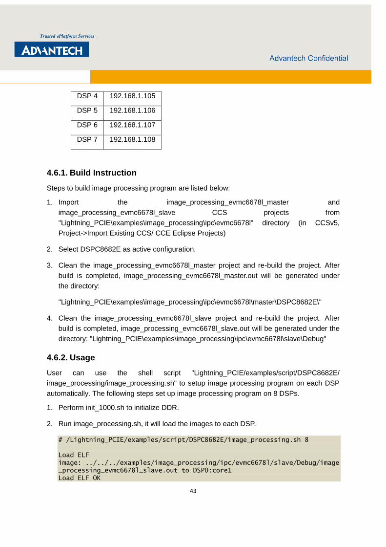
4.6.1. Build Instruction
Steps to build image processing program are listed below:
1. Import the image_processing_evmc6678l_master and
image_processing_evmc6678l_slave CCS projects from
"Lightning_PCIE\examples\image_processing\ipc\evmc6678l" directory (in CCSv5,
Project->Import Existing CCS/ CCE Eclipse Projects)
2. Select DSPC8682E as active configuration.
3. Clean the image_processing_evmc6678l_master project and re-build the project. After
build is completed, image_processing_evmc6678l_master.out will be generated under
the directory:
"Lightning_PCIE\examples\image_processing\ipc\evmc6678l\master\DSPC8682E\"
4. Clean the image_processing_evmc6678l_slave project and re-build the project. After
build is completed, image_processing_evmc6678l_slave.out will be generated under the
directory: "Lightning_PCIE\examples\image_processing\ipc\evmc6678l\slave\Debug"
4.6.2. Usage
User can use the shell script "Lightning_PCIE/examples/script/DSPC8682E/
image_processing/image_processing.sh" to setup image processing program on each DSP
automatically. The following steps set up image processing program on 8 DSPs.
1. Perform init_1000.sh to initialize DDR.
2. Run image_processing.sh, it will load the images to each DSP.
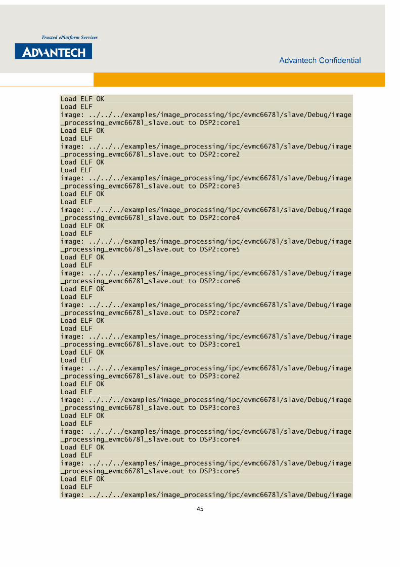
# /Lightning_PCIE/examples/script/DSPC8682E/image_processing.sh 8
Load ELF
image: ../../../examples/image_processing/ipc/evmc6678l/slave/Debug/image
_processing_evmc6678l_slave.out to DSP0:core1
Load ELF OK
44
Load ELF
image: ../../../examples/image_processing/ipc/evmc6678l/slave/Debug/image
_processing_evmc6678l_slave.out to DSP0:core2
Load ELF OK
Load ELF
image: ../../../examples/image_processing/ipc/evmc6678l/slave/Debug/image
_processing_evmc6678l_slave.out to DSP0:core3
Load ELF OK
Load ELF
image: ../../../examples/image_processing/ipc/evmc6678l/slave/Debug/image
_processing_evmc6678l_slave.out to DSP0:core4
Load ELF OK
Load ELF
image: ../../../examples/image_processing/ipc/evmc6678l/slave/Debug/image
_processing_evmc6678l_slave.out to DSP0:core5
Load ELF OK
Load ELF
image: ../../../examples/image_processing/ipc/evmc6678l/slave/Debug/image
_processing_evmc6678l_slave.out to DSP0:core6
Load ELF OK
Load ELF
image: ../../../examples/image_processing/ipc/evmc6678l/slave/Debug/image
_processing_evmc6678l_slave.out to DSP0:core7
Load ELF OK
Load ELF
image: ../../../examples/image_processing/ipc/evmc6678l/slave/Debug/image
_processing_evmc6678l_slave.out to DSP1:core1
Load ELF OK
Load ELF
image: ../../../examples/image_processing/ipc/evmc6678l/slave/Debug/image
_processing_evmc6678l_slave.out to DSP1:core2
Load ELF OK
Load ELF
image: ../../../examples/image_processing/ipc/evmc6678l/slave/Debug/image
_processing_evmc6678l_slave.out to DSP1:core3
Load ELF OK
Load ELF
image: ../../../examples/image_processing/ipc/evmc6678l/slave/Debug/image
_processing_evmc6678l_slave.out to DSP1:core4
Load ELF OK
Load ELF
image: ../../../examples/image_processing/ipc/evmc6678l/slave/Debug/image
_processing_evmc6678l_slave.out to DSP1:core5
Load ELF OK
Load ELF
image: ../../../examples/image_processing/ipc/evmc6678l/slave/Debug/image
_processing_evmc6678l_slave.out to DSP1:core6
Load ELF OK
Load ELF
image: ../../../examples/image_processing/ipc/evmc6678l/slave/Debug/image
_processing_evmc6678l_slave.out to DSP1:core7
45
Load ELF OK
Load ELF
image: ../../../examples/image_processing/ipc/evmc6678l/slave/Debug/image
_processing_evmc6678l_slave.out to DSP2:core1
Load ELF OK
Load ELF
image: ../../../examples/image_processing/ipc/evmc6678l/slave/Debug/image
_processing_evmc6678l_slave.out to DSP2:core2
Load ELF OK
Load ELF
image: ../../../examples/image_processing/ipc/evmc6678l/slave/Debug/image
_processing_evmc6678l_slave.out to DSP2:core3
Load ELF OK
Load ELF
image: ../../../examples/image_processing/ipc/evmc6678l/slave/Debug/image
_processing_evmc6678l_slave.out to DSP2:core4
Load ELF OK
Load ELF
image: ../../../examples/image_processing/ipc/evmc6678l/slave/Debug/image
_processing_evmc6678l_slave.out to DSP2:core5
Load ELF OK
Load ELF
image: ../../../examples/image_processing/ipc/evmc6678l/slave/Debug/image
_processing_evmc6678l_slave.out to DSP2:core6
Load ELF OK
Load ELF
image: ../../../examples/image_processing/ipc/evmc6678l/slave/Debug/image
_processing_evmc6678l_slave.out to DSP2:core7
Load ELF OK
Load ELF
image: ../../../examples/image_processing/ipc/evmc6678l/slave/Debug/image
_processing_evmc6678l_slave.out to DSP3:core1
Load ELF OK
Load ELF
image: ../../../examples/image_processing/ipc/evmc6678l/slave/Debug/image
_processing_evmc6678l_slave.out to DSP3:core2
Load ELF OK
Load ELF
image: ../../../examples/image_processing/ipc/evmc6678l/slave/Debug/image
_processing_evmc6678l_slave.out to DSP3:core3
Load ELF OK
Load ELF
image: ../../../examples/image_processing/ipc/evmc6678l/slave/Debug/image
_processing_evmc6678l_slave.out to DSP3:core4
Load ELF OK
Load ELF
image: ../../../examples/image_processing/ipc/evmc6678l/slave/Debug/image
_processing_evmc6678l_slave.out to DSP3:core5
Load ELF OK
Load ELF
image: ../../../examples/image_processing/ipc/evmc6678l/slave/Debug/image
46
_processing_evmc6678l_slave.out to DSP3:core6
Load ELF OK
Load ELF
image: ../../../examples/image_processing/ipc/evmc6678l/slave/Debug/image
_processing_evmc6678l_slave.out to DSP3:core7
Load ELF OK
Load ELF
image: ../../../examples/image_processing/ipc/evmc6678l/slave/Debug/image
_processing_evmc6678l_slave.out to DSP4:core1
Load ELF OK
Load ELF
image: ../../../examples/image_processing/ipc/evmc6678l/slave/Debug/image
_processing_evmc6678l_slave.out to DSP4:core2
Load ELF OK
Load ELF
image: ../../../examples/image_processing/ipc/evmc6678l/slave/Debug/image
_processing_evmc6678l_slave.out to DSP4:core3
Load ELF OK
Load ELF
image: ../../../examples/image_processing/ipc/evmc6678l/slave/Debug/image
_processing_evmc6678l_slave.out to DSP4:core4
Load ELF OK
Load ELF
image: ../../../examples/image_processing/ipc/evmc6678l/slave/Debug/image
_processing_evmc6678l_slave.out to DSP4:core5
Load ELF OK
Load ELF
image: ../../../examples/image_processing/ipc/evmc6678l/slave/Debug/image
_processing_evmc6678l_slave.out to DSP4:core6
Load ELF OK
Load ELF
image: ../../../examples/image_processing/ipc/evmc6678l/slave/Debug/image
_processing_evmc6678l_slave.out to DSP4:core7
Load ELF OK
Load ELF
image: ../../../examples/image_processing/ipc/evmc6678l/slave/Debug/image
_processing_evmc6678l_slave.out to DSP5:core1
Load ELF OK
Load ELF
image: ../../../examples/image_processing/ipc/evmc6678l/slave/Debug/image
_processing_evmc6678l_slave.out to DSP5:core2
Load ELF OK
Load ELF
image: ../../../examples/image_processing/ipc/evmc6678l/slave/Debug/image
_processing_evmc6678l_slave.out to DSP5:core3
Load ELF OK
Load ELF
image: ../../../examples/image_processing/ipc/evmc6678l/slave/Debug/image
_processing_evmc6678l_slave.out to DSP5:core4
Load ELF OK
Load ELF

47
image: ../../../examples/image_processing/ipc/evmc6678l/slave/Debug/image
_processing_evmc6678l_slave.out to DSP5:core5
Load ELF OK
Load ELF
image: ../../../examples/image_processing/ipc/evmc6678l/slave/Debug/image
_processing_evmc6678l_slave.out to DSP5:core6
Load ELF OK
Load ELF
image: ../../../examples/image_processing/ipc/evmc6678l/slave/Debug/image
_processing_evmc6678l_slave.out to DSP5:core7
Load ELF OK
Load ELF
image: ../../../examples/image_processing/ipc/evmc6678l/slave/Debug/image
_processing_evmc6678l_slave.out to DSP6:core1
Load ELF OK
Load ELF
image: ../../../examples/image_processing/ipc/evmc6678l/slave/Debug/image
_processing_evmc6678l_slave.out to DSP6:core2
Load ELF OK
Load ELF
image: ../../../examples/image_processing/ipc/evmc6678l/slave/Debug/image
_processing_evmc6678l_slave.out to DSP6:core3
Load ELF OK
Load ELF
image: ../../../examples/image_processing/ipc/evmc6678l/slave/Debug/image
_processing_evmc6678l_slave.out to DSP6:core4
Load ELF OK
Load ELF
image: ../../../examples/image_processing/ipc/evmc6678l/slave/Debug/image
_processing_evmc6678l_slave.out to DSP6:core5
Load ELF OK
Load ELF
image: ../../../examples/image_processing/ipc/evmc6678l/slave/Debug/image
_processing_evmc6678l_slave.out to DSP6:core6
Load ELF OK
Load ELF
image: ../../../examples/image_processing/ipc/evmc6678l/slave/Debug/image
_processing_evmc6678l_slave.out to DSP6:core7
Load ELF OK
Load ELF
image: ../../../examples/image_processing/ipc/evmc6678l/slave/Debug/image
_processing_evmc6678l_slave.out to DSP7:core1
Load ELF OK
Load ELF
image: ../../../examples/image_processing/ipc/evmc6678l/slave/Debug/image
_processing_evmc6678l_slave.out to DSP7:core2
Load ELF OK
Load ELF
image: ../../../examples/image_processing/ipc/evmc6678l/slave/Debug/image
_processing_evmc6678l_slave.out to DSP7:core3
Load ELF OK
48
Load ELF
image: ../../../examples/image_processing/ipc/evmc6678l/slave/Debug/image
_processing_evmc6678l_slave.out to DSP7:core4
Load ELF OK
Load ELF
image: ../../../examples/image_processing/ipc/evmc6678l/slave/Debug/image
_processing_evmc6678l_slave.out to DSP7:core5
Load ELF OK
Load ELF
image: ../../../examples/image_processing/ipc/evmc6678l/slave/Debug/image
_processing_evmc6678l_slave.out to DSP7:core6
Load ELF OK
Load ELF
image: ../../../examples/image_processing/ipc/evmc6678l/slave/Debug/image
_processing_evmc6678l_slave.out to DSP7:core7
Load ELF OK
Load ELF
image: ../../../examples/image_processing/ipc/evmc6678l/master/DSPC8682E/
image_processing_evmc6678l_master.out to DSP0:core0
Load ELF OK
Load ELF
image: ../../../examples/image_processing/ipc/evmc6678l/master/DSPC8682E/
image_processing_evmc6678l_master.out to DSP1:core0
Load ELF OK
Load ELF
image: ../../../examples/image_processing/ipc/evmc6678l/master/DSPC8682E/
image_processing_evmc6678l_master.out to DSP2:core0
Load ELF OK
Load ELF
image: ../../../examples/image_processing/ipc/evmc6678l/master/DSPC8682E/
image_processing_evmc6678l_master.out to DSP3:core0
Load ELF OK
Load ELF
image: ../../../examples/image_processing/ipc/evmc6678l/master/DSPC8682E/
image_processing_evmc6678l_master.out to DSP4:core0
Load ELF OK
Load ELF
image: ../../../examples/image_processing/ipc/evmc6678l/master/DSPC8682E/
image_processing_evmc6678l_master.out to DSP5:core0
Load ELF OK
Load ELF
image: ../../../examples/image_processing/ipc/evmc6678l/master/DSPC8682E/
image_processing_evmc6678l_master.out to DSP6:core0
Load ELF OK
Load ELF
image: ../../../examples/image_processing/ipc/evmc6678l/master/DSPC8682E/
image_processing_evmc6678l_master.out to DSP7:core0
Load ELF OK
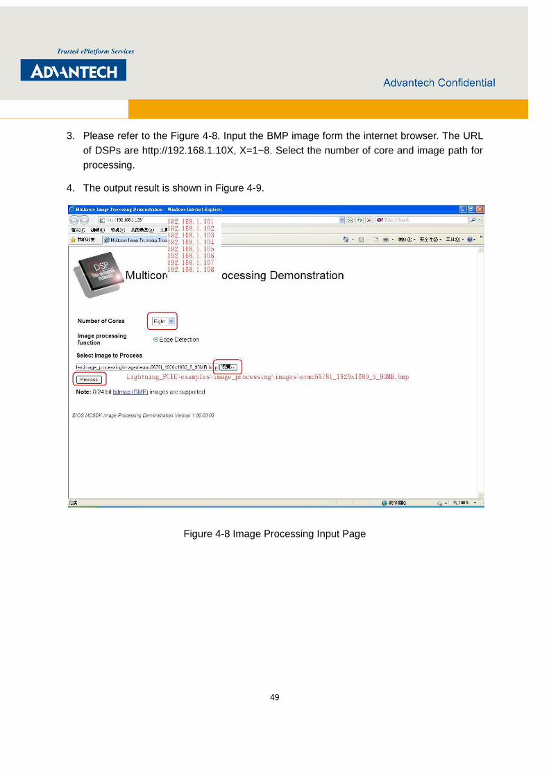
49
3. Please refer to the Figure 4-8. Input the BMP image form the internet browser. The URL
of DSPs are http://192.168.1.10X, X=1~8. Select the number of core and image path for
processing.
4. The output result is shown in Figure 4-9.
Figure 4-8 Image Processing Input Page
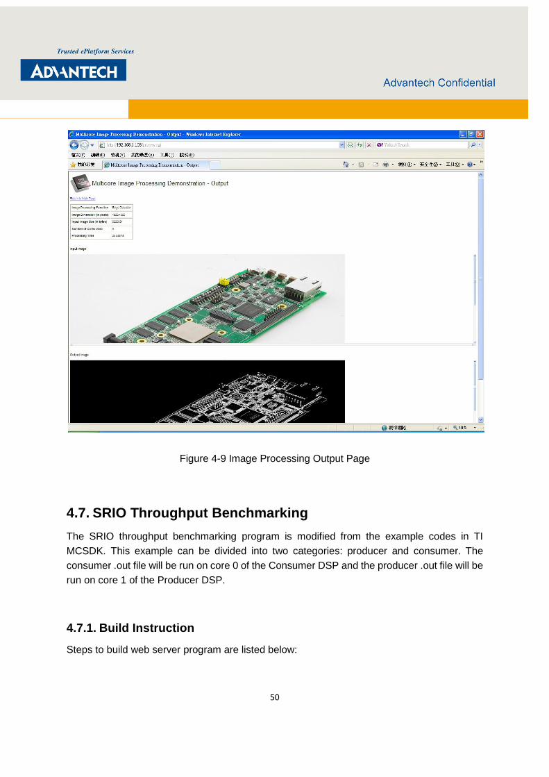
50
Figure 4-9 Image Processing Output Page
4.7. SRIO Throughput Benchmarking
The SRIO throughput benchmarking program is modified from the example codes in TI
MCSDK. This example can be divided into two categories: producer and consumer. The
consumer .out file will be run on core 0 of the Consumer DSP and the producer .out file will be
run on core 1 of the Producer DSP.
4.7.1. Build Instruction
Steps to build web server program are listed below:
51
1. Import the SRIO_TputBenchmarkingTestProject CCS project from
"Lightning_PCIE\examples\srio_throughput\dsp" directory (in CCSv5, Project->Import
Existing CCS/ CCE Eclipse Projects)
2. Select DSPC8682E_Producer and DSPC8682E_Consumer as active configuration.
3. Clean the SRIO_TputBenchmarkingTestProject project and re-build the project. After
build is completed, SRIO_Tput_producer.out and SRIO_Tput_producer.map will be
generated under "Lightning_PCIE\examples\srio_throughput\dsp
\DSPC8682E_Producer" directory; SRIO_Tput_consumer.out and
SRIO_Tput_consumer.map will be generated under "
Lightning_PCIE\examples\srio_throughput\dsp\DSPC8682E_Consumer" directory.
4.7.2. Usage
User can use the shell script
"Lightning_PCIE/examples/script/DSPC8682E/srio_throughput/load_run_test.sh" to setup
SRIO throughput benchmarking program on each DSP automatically. The following steps set
up SRIO program on specified DSPs.
1. Perform the init_1000.sh to initialize DDR.
2. Perform the load_run_test.sh to load SRIO_Tput_producer.out file and
SRIO_Tput_consumer.out file into specified DSP.
The command syntax is:
./load_run_test.sh [Producer DSP ID#] [Consumer DSP ID#] [Port Width] [Producer
SRIO Port#] [Consumer SRIO Port#]
The detailed description of each parameter is shown below:
1. [Producer DSP ID#]: Producer DSP ID start from 0
2. [Consumer DSP ID#]: Consumer DSP ID start from 0
3. [Port Width]: 2 for two 1x and one 2x
4. [Producer SRIO Port#]: Port1 or Port2
5. [Consumer SRIO Port#]: Port0 or Port2
The following sample console output is to run SRIO throughput benchmarking on DSP0 port
2 as producer and DSP7 port2 as consumer.

52
# /Lightning_PCIE/examples/script/DSPC8682E/srio_throughput/load_run_test.sh
0 7 2 2 2
Load ELF
image: ../../../examples/srio_throughput/dsp/DSPC8682E_Consumer/SRIO_Tput_co
nsumer.out to DSP7:core0
Load ELF OK
Load ELF
image: ../../../examples/srio_throughput/dsp/DSPC8682E_Producer/SRIO_Tput_pr
oducer.out to DSP0:core1
Load ELF OK
Check DSP state... done.
********************************
*********** PRODUCER ***********
********************************
WARNING: Please ensure that the CONSUMER is executing before running the
PRODUCER!!
Debug: Waiting for module reset...
Debug: Waiting for module local reset...
Debug: Waiting for SRIO ports to be operational...
Debug: SRIO port 0 is operational.
Debug: SRIO port 1 is NOT operational.
Debug: SRIO port 2 is operational.
Debug: Lanes status shows lanes formed as two 1x ports and one 2x port
Debug: Running test in polled mode.
Debug: SRIO Driver handle 0x821700.
Latency: (DIO_NW, 5.000GBaud, 1X, tab delimited)
Core Lanes Speed Conn MsgType PktSize NumPkts MnLCycs AgLCycs MxLCycs
1 1 5.000 B-S-B DIO_NW 4 100 883 888 1370
1 1 5.000 B-S-B DIO_NW 8 100 865 883 973
1 1 5.000 B-S-B DIO_NW 16 100 900 903 991
1 1 5.000 B-S-B DIO_NW 32 100 955 964 1063
1 1 5.000 B-S-B DIO_NW 64 100 1063 1079 1170
1 1 5.000 B-S-B DIO_NW 128 100 1296 1299 1390
1 1 5.000 B-S-B DIO_NW 256 100 1728 1731 1822
1 1 5.000 B-S-B DIO_NW 512 100 1999 2016 2110
1 1 5.000 B-S-B DIO_NW 1024 100 2574 2577 2669
1 1 5.000 B-S-B DIO_NW 2048 100 3690 3700 3785
1 1 5.000 B-S-B DIO_NW 4096 100 5923 5943 6035
1 1 5.000 B-S-B DIO_NW 8192 100 10386 10392 10481
Throughput: (TX side, DIO_NW, 5.000GBaud, 1X, tab delimited)
Core Lanes Speed Conn MsgType OHBytes PktSize Pacing Thruput PktsSec. NumPkts PktLoss AgPCycs AgLCycs AgICycs AgOCycs Seconds
1 1 5.000 B-S-B DIO_NW 16 4 0 85.33 2666666.75 12600000 No 375 319 41 15 4.73
1 1 5.000 B-S-B DIO_NW 16 8 0 170.67 2666666.75 12600000 No 375 319 41 15 4.73
1 1 5.000 B-S-B DIO_NW 16 16 0 341.33 2666666.75 12600000 No 375 319 41 15 4.73
1 1 5.000 B-S-B DIO_NW 16 32 0 682.67 2666666.75 12600000 No 375 319 41 15 4.73
1 1 5.000 B-S-B DIO_NW 16 64 0 1365.33 2666666.75 12600000 No 375 319 41 15 4.73
1 1 5.000 B-S-B DIO_NW 16 128 0 2730.67 2666666.75 12600000 No 375 319 41 15 4.73
1 1 5.000 B-S-B DIO_NW 16 256 159 3611.99 1763668.38 8400000 No 576 319 233 15 4.76
1 1 5.000 B-S-B DIO_NW 16 512 718 3631.32 886524.81 4400000 No 1128 320 793 15 4.96
1 1 5.000 B-S-B DIO_NW 16 1024 1823 3665.32 447427.28 2400000 No 2235 321 1899 15 5.36
1 1 5.000 B-S-B DIO_NW 16 2048 4064 3662.87 223563.61 1200000 No 4473 319 4139 15 5.37
1 1 5.000 B-S-B DIO_NW 16 4096 8515 3671.48 112044.82 600000 No 8925 319 8591 15 5.36
1 1 5.000 B-S-B DIO_NW 16 8192 17447 3669.63 55994.18 400000 No 17859 321 17523 15 7.14

53
Latency: (DIO_NR, 5.000GBaud, 1X, tab delimited)
Core Lanes Speed Conn MsgType PktSize NumPkts MnLCycs AgLCycs MxLCycs
1 1 5.000 B-S-B DIO_NR 4 100 1274 1303 1501
1 1 5.000 B-S-B DIO_NR 8 100 1274 1298 1501
1 1 5.000 B-S-B DIO_NR 16 100 1274 1322 1501
1 1 5.000 B-S-B DIO_NR 32 100 1274 1380 1508
1 1 5.000 B-S-B DIO_NR 64 100 1274 1485 1606
1 1 5.000 B-S-B DIO_NR 128 100 1274 1699 1823
1 1 5.000 B-S-B DIO_NR 256 100 1274 2150 2278
1 1 5.000 B-S-B DIO_NR 512 100 1274 2430 2558
1 1 5.000 B-S-B DIO_NR 1024 100 1274 2983 3118
1 1 5.000 B-S-B DIO_NR 2048 100 1274 4084 4203
1 1 5.000 B-S-B DIO_NR 4096 100 1274 6308 6408
1 1 5.000 B-S-B DIO_NR 8192 100 1274 10797 10915
Throughput: (TX side, DIO_NR, 5.000GBaud, 1X, tab delimited)
Core Lanes Speed Conn MsgType OHBytes PktSize Pacing Thruput PktsSec. NumPkts PktLoss AgPCycs AgLCycs AgICycs AgOCycs Seconds
1 1 5.000 B-S-B DIO_NR 28 4 0 29.74 929368.00 4600000 No 1076 326 41 735 4.95
1 1 5.000 B-S-B DIO_NR 28 8 0 59.48 929368.00 4600000 No 1076 326 41 735 4.95
1 1 5.000 B-S-B DIO_NR 28 16 0 115.84 904977.38 4400000 No 1105 326 41 764 4.86
1 1 5.000 B-S-B DIO_NR 28 32 0 222.22 868055.56 4200000 No 1152 320 41 817 4.84
1 1 5.000 B-S-B DIO_NR 28 64 0 404.74 790513.81 4000000 No 1265 321 41 929 5.06
1 1 5.000 B-S-B DIO_NR 28 128 0 690.49 674308.81 3400000 No 1483 321 41 1147 5.04
1 1 5.000 B-S-B DIO_NR 28 256 0 1063.34 519210.81 2600000 No 1926 320 233 1591 5.01
1 1 5.000 B-S-B DIO_NR 28 512 0 1859.28 453926.47 2400000 No 2203 320 793 1868 5.29
1 1 5.000 B-S-B DIO_NR 28 1024 0 2976.74 363372.09 1800000 No 2752 320 1899 2417 4.95
1 1 5.000 B-S-B DIO_NR 28 2048 0 4243.46 259000.27 1400000 No 3861 321 4139 3525 5.41
1 1 5.000 B-S-B DIO_NR 28 4096 0 5391.25 164527.81 1000000 No 6078 320 8591 5743 6.08
1 1 5.000 B-S-B DIO_NR 28 8192 0 6195.50 94535.83 600000 No 10578 326 17523 10237 6.35
Latency: (Type-11, 5.000GBaud, 1X, tab delimited)
Core Lanes Speed Conn MsgType PktSize NumPkts MnLCycs AgLCycs MxLCycs
1 1 5.000 B-S-B Type-11 16 100 2101 1303 1501
1 1 5.000 B-S-B Type-11 32 100 2209 1298 1501
1 1 5.000 B-S-B Type-11 64 100 2389 1322 1501
1 1 5.000 B-S-B Type-11 128 100 2566 1380 1508
1 1 5.000 B-S-B Type-11 256 100 3133 1485 1606
1 1 5.000 B-S-B Type-11 512 100 3274 1699 1823
1 1 5.000 B-S-B Type-11 1024 100 3877 2150 2278
1 1 5.000 B-S-B Type-11 2048 100 4957 2430 2558
1 1 5.000 B-S-B Type-11 4096 100 7192 2983 3118
Throughput: (TX side, Type-11, 5.000GBaud, 1X, tab delimited)
Core Lanes Speed Conn MsgType OHBytes PktSize Pacing Thruput PktsSec. NumPkts PktLoss AgPCycs AgLCycs AgICycs AgOCycs Seconds
1 1 5.000 B-S-B Type-11 24 16 298 102.65 801924.63 4000000 No 1247 223 1007 17 4.99
1 1 5.000 B-S-B Type-11 24 32 297 205.29 801924.63 4000000 No 1247 224 1006 17 4.99
1 1 5.000 B-S-B Type-11 24 64 297 410.59 801924.63 4000000 No 1247 223 1007 17 4.99
1 1 5.000 B-S-B Type-11 24 128 297 821.17 801924.63 4000000 No 1247 223 1007 17 4.99
1 1 5.000 B-S-B Type-11 24 256 297 1642.34 801924.63 4000000 No 1247 223 1007 17 4.99
1 1 5.000 B-S-B Type-11 24 512 297 3284.68 801924.63 4000000 No 1247 223 1007 17 4.99
1 1 5.000 B-S-B Type-11 24 1024 297 6569.37 801924.63 4000000 No 1247 223 1007 17 4.99
1 1 5.000 B-S-B Type-11 24 2048 0 7291.50 445037.84 2400000 No 2247 227 2003 17 5.39
1 1 5.000 B-S-B Type-11 24 4096 0 7291.50 222518.92 1200000 No 4494 221 4256 17 5.39
SRIO PRODUCER DSP0 to CONSUMER DSP7 throughput test completed
3. There are four prewritten shell script under the same directory, and user can directly use
them to demonstrate SRIO thoughtput example with different configuration.
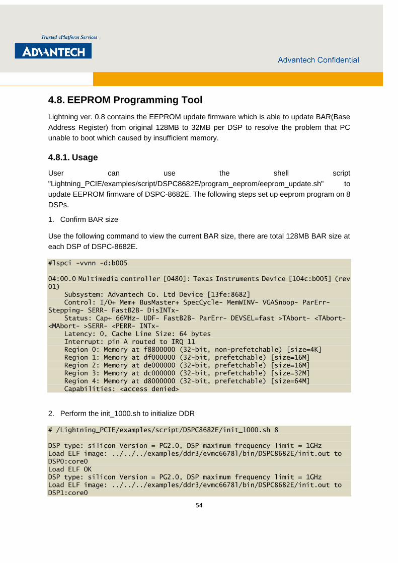
54
4.8. EEPROM Programming Tool
Lightning ver. 0.8 contains the EEPROM update firmware which is able to update BAR(Base
Address Register) from original 128MB to 32MB per DSP to resolve the problem that PC
unable to boot which caused by insufficient memory.
4.8.1. Usage
User can use the shell script
"Lightning_PCIE/examples/script/DSPC8682E/program_eeprom/eeprom_update.sh" to
update EEPROM firmware of DSPC-8682E. The following steps set up eeprom program on 8
DSPs.
1. Confirm BAR size
Use the following command to view the current BAR size, there are total 128MB BAR size at
each DSP of DSPC-8682E.
#lspci -vvnn -d:b005
04:00.0 Multimedia controller [0480]: Texas Instruments Device [104c:b005] (rev
01)
Subsystem: Advantech Co. Ltd Device [13fe:8682]
Control: I/O+ Mem+ BusMaster+ SpecCycle- MemWINV- VGASnoop- ParErr-
Stepping- SERR- FastB2B- DisINTx-
Status: Cap+ 66MHz- UDF- FastB2B- ParErr- DEVSEL=fast >TAbort- <TAbort-
<MAbort- >SERR- <PERR- INTx-
Latency: 0, Cache Line Size: 64 bytes
Interrupt: pin A routed to IRQ 11
Region 0: Memory at f8800000 (32-bit, non-prefetchable) [size=4K]
Region 1: Memory at df000000 (32-bit, prefetchable) [size=16M]
Region 2: Memory at de000000 (32-bit, prefetchable) [size=16M]
Region 3: Memory at dc000000 (32-bit, prefetchable) [size=32M]
Region 4: Memory at d8000000 (32-bit, prefetchable) [size=64M]
Capabilities: <access denied>
2. Perform the init_1000.sh to initialize DDR
# /Lightning_PCIE/examples/script/DSPC8682E/init_1000.sh 8
DSP type: silicon Version = PG2.0, DSP maximum frequency limit = 1GHz
Load ELF image: ../../../examples/ddr3/evmc6678l/bin/DSPC8682E/init.out to
DSP0:core0
Load ELF OK
DSP type: silicon Version = PG2.0, DSP maximum frequency limit = 1GHz
Load ELF image: ../../../examples/ddr3/evmc6678l/bin/DSPC8682E/init.out to
DSP1:core0

55
Load ELF OK
DSP type: silicon Version = PG2.0, DSP maximum frequency limit = 1GHz
Load ELF image: ../../../examples/ddr3/evmc6678l/bin/DSPC8682E/init.out to
DSP2:core0
Load ELF OK
DSP type: silicon Version = PG2.0, DSP maximum frequency limit = 1GHz
Load ELF image: ../../../examples/ddr3/evmc6678l/bin/DSPC8682E/init.out to
DSP3:core0
Load ELF OK
DSP type: silicon Version = PG2.0, DSP maximum frequency limit = 1GHz
Load ELF image: ../../../examples/ddr3/evmc6678l/bin/DSPC8682E/init.out to
DSP4:core0
Load ELF OK
DSP type: silicon Version = PG2.0, DSP maximum frequency limit = 1GHz
Load ELF image: ../../../examples/ddr3/evmc6678l/bin/DSPC8682E/init.out to
DSP5:core0
Load ELF OK
DSP type: silicon Version = PG2.0, DSP maximum frequency limit = 1GHz
Load ELF image: ../../../examples/ddr3/evmc6678l/bin/DSPC8682E/init.out to
DSP6:core0
Load ELF OK
DSP type: silicon Version = PG2.0, DSP maximum frequency limit = 1GHz
Load ELF image: ../../../examples/ddr3/evmc6678l/bin/DSPC8682E/init.out to
DSP7:core0
Load ELF OK
3. Download burning program into DSP
Run eeprom_update.sh script to download burning program into each DSP.
# /Lightning_PCIE/examples/script/DSPC8682E/program_eeprom/eeprom_update.sh 8
Load Binary
file: ../../../tools/program_eeprom/pcieboot/bin/eeprom_0_post_8682.bin to
DSP0, start address 0x0c000000, Size 0x00000000
Written to dsp 3880 bytes
Time measured: 74024 us
Load Binary OK
Load Binary
file: ../../../tools/program_eeprom/pcieboot/bin/eeprom_1_post_8682.bin to
DSP0, start address 0x0c00ffdc, Size 0x00000000
Written to dsp 3848 bytes
Time measured: 2825 us
Load Binary OK
Load ELF
image: ../../../tools/program_eeprom/writer/DSPC8682_PCIE/868x_eeprom_writer
.out to DSP0:core0
Load ELF OK
Load Binary
file: ../../../tools/program_eeprom/pcieboot/bin/eeprom_0_post_8682.bin to

56
DSP1, start address 0x0c000000, Size 0x00000000
Written to dsp 3880 bytes
Time measured: 73142 us
Load Binary OK
Load Binary
file: ../../../tools/program_eeprom/pcieboot/bin/eeprom_1_post_8682.bin to
DSP1, start address 0x0c00ffdc, Size 0x00000000
Written to dsp 3848 bytes
Time measured: 2804 us
Load Binary OK
Load ELF
image: ../../../tools/program_eeprom/writer/DSPC8682_PCIE/868x_eeprom_writer
.out to DSP1:core0
Load ELF OK
Load Binary
file: ../../../tools/program_eeprom/pcieboot/bin/eeprom_0_post_8682.bin to
DSP2, start address 0x0c000000, Size 0x00000000
Written to dsp 3880 bytes
Time measured: 74298 us
Load Binary OK
Load Binary
file: ../../../tools/program_eeprom/pcieboot/bin/eeprom_1_post_8682.bin to
DSP2, start address 0x0c00ffdc, Size 0x00000000
Written to dsp 3848 bytes
Time measured: 2699 us
Load Binary OK
Load ELF
image: ../../../tools/program_eeprom/writer/DSPC8682_PCIE/868x_eeprom_writer
.out to DSP2:core0
Load ELF OK
Load Binary
file: ../../../tools/program_eeprom/pcieboot/bin/eeprom_0_post_8682.bin to
DSP3, start address 0x0c000000, Size 0x00000000
Written to dsp 3880 bytes
Time measured: 70478 us
Load Binary OK
Load Binary
file: ../../../tools/program_eeprom/pcieboot/bin/eeprom_1_post_8682.bin to
DSP3, start address 0x0c00ffdc, Size 0x00000000
Written to dsp 3848 bytes
Time measured: 2685 us
Load Binary OK
Load ELF
image: ../../../tools/program_eeprom/writer/DSPC8682_PCIE/868x_eeprom_writer
.out to DSP3:core0
Load ELF OK
Load Binary
file: ../../../tools/program_eeprom/pcieboot/bin/eeprom_0_post_8682.bin to
DSP4, start address 0x0c000000, Size 0x00000000
Written to dsp 3880 bytes
Time measured: 75110 us
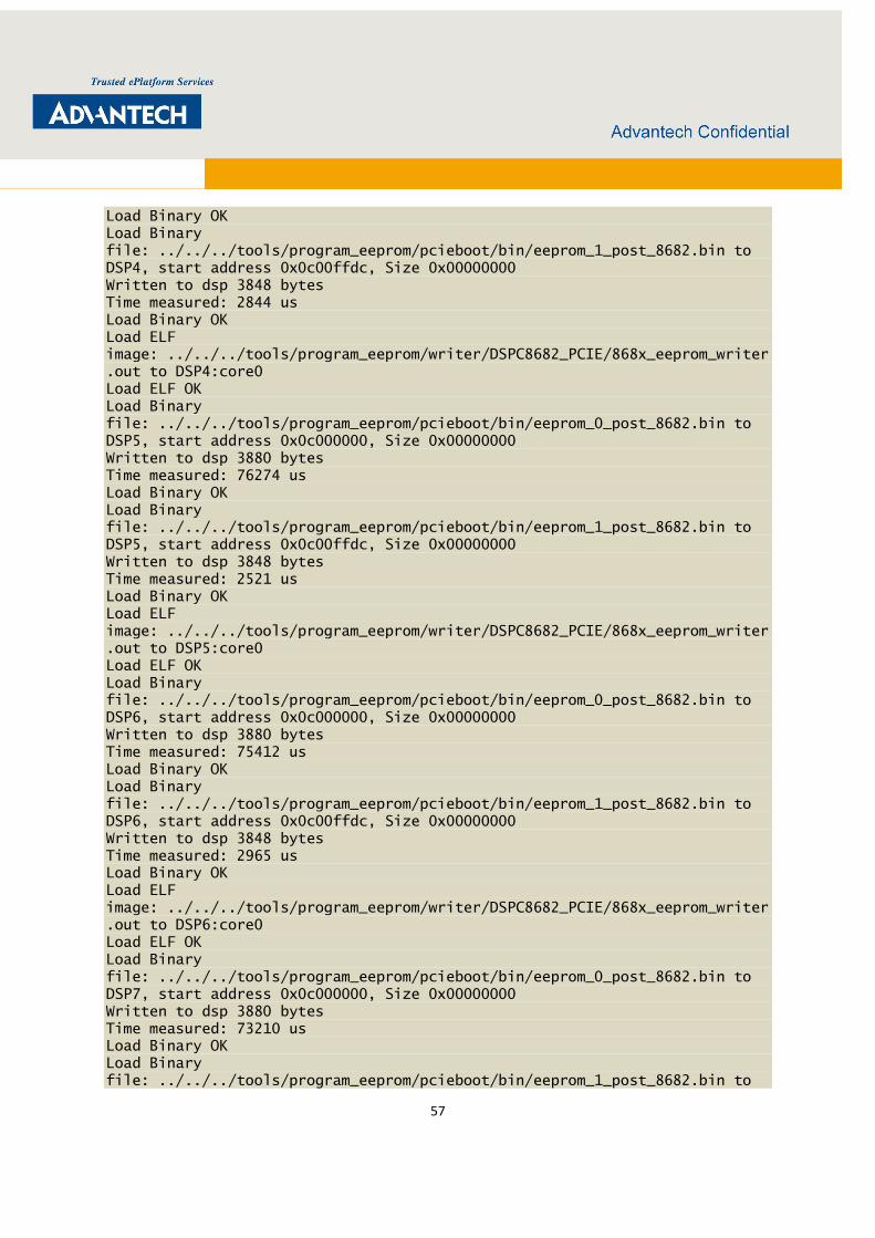
57
Load Binary OK
Load Binary
file: ../../../tools/program_eeprom/pcieboot/bin/eeprom_1_post_8682.bin to
DSP4, start address 0x0c00ffdc, Size 0x00000000
Written to dsp 3848 bytes
Time measured: 2844 us
Load Binary OK
Load ELF
image: ../../../tools/program_eeprom/writer/DSPC8682_PCIE/868x_eeprom_writer
.out to DSP4:core0
Load ELF OK
Load Binary
file: ../../../tools/program_eeprom/pcieboot/bin/eeprom_0_post_8682.bin to
DSP5, start address 0x0c000000, Size 0x00000000
Written to dsp 3880 bytes
Time measured: 76274 us
Load Binary OK
Load Binary
file: ../../../tools/program_eeprom/pcieboot/bin/eeprom_1_post_8682.bin to
DSP5, start address 0x0c00ffdc, Size 0x00000000
Written to dsp 3848 bytes
Time measured: 2521 us
Load Binary OK
Load ELF
image: ../../../tools/program_eeprom/writer/DSPC8682_PCIE/868x_eeprom_writer
.out to DSP5:core0
Load ELF OK
Load Binary
file: ../../../tools/program_eeprom/pcieboot/bin/eeprom_0_post_8682.bin to
DSP6, start address 0x0c000000, Size 0x00000000
Written to dsp 3880 bytes
Time measured: 75412 us
Load Binary OK
Load Binary
file: ../../../tools/program_eeprom/pcieboot/bin/eeprom_1_post_8682.bin to
DSP6, start address 0x0c00ffdc, Size 0x00000000
Written to dsp 3848 bytes
Time measured: 2965 us
Load Binary OK
Load ELF
image: ../../../tools/program_eeprom/writer/DSPC8682_PCIE/868x_eeprom_writer
.out to DSP6:core0
Load ELF OK
Load Binary
file: ../../../tools/program_eeprom/pcieboot/bin/eeprom_0_post_8682.bin to
DSP7, start address 0x0c000000, Size 0x00000000
Written to dsp 3880 bytes
Time measured: 73210 us
Load Binary OK
Load Binary
file: ../../../tools/program_eeprom/pcieboot/bin/eeprom_1_post_8682.bin to
58
DSP7, start address 0x0c00ffdc, Size 0x00000000
Written to dsp 3848 bytes
Time measured: 2774 us
Load Binary OK
Load ELF
image: ../../../tools/program_eeprom/writer/DSPC8682_PCIE/868x_eeprom_writer
.out to DSP7:core0
Load ELF OK
The system will download burning program into each DSP, and pops up 8 windows to show
current update status at each DSP. It may take a few minutes and DO NOT turn off the power
supply at this time.
4. Confirm update status
When Terminal shows EEPROM update completely, it means update successfully. Please
confirm that 8 DSPs show the same message and then follow the correct procedure to shut
your PC down safely.
Check DSP state... done.
[DSP0] eeprom_flash bank 0 start
[DSP0] eeprom_flash bank 0 PASS
[DSP0] eeprom_flash bank 1 start
[DSP0] eeprom_flash bank 1 PASS
[DSP0] EEPROM update completely
Check DSP state... done.
[DSP1] eeprom_flash bank 0 start
[DSP1] eeprom_flash bank 0 PASS
[DSP1] eeprom_flash bank 1 start
[DSP1] eeprom_flash bank 1 PASS
[DSP1] EEPROM update completely
Check DSP state... done.
[DSP2] eeprom_flash bank 0 start
[DSP2] eeprom_flash bank 0 PASS
[DSP2] eeprom_flash bank 1 start
[DSP2] eeprom_flash bank 1 PASS
[DSP2] EEPROM update completely
59
Check DSP state... done.
[DSP3] eeprom_flash bank 0 start
[DSP3] eeprom_flash bank 0 PASS
[DSP3] eeprom_flash bank 1 start
[DSP3] eeprom_flash bank 1 PASS
[DSP3] EEPROM update completely
Check DSP state... done.
[DSP4] eeprom_flash bank 0 start
[DSP4] eeprom_flash bank 0 PASS
[DSP4] eeprom_flash bank 1 start
[DSP4] eeprom_flash bank 1 PASS
[DSP4] EEPROM update completely
Check DSP state... done.
[DSP5] eeprom_flash bank 0 start
[DSP5] eeprom_flash bank 0 PASS
[DSP5] eeprom_flash bank 1 start
[DSP5] eeprom_flash bank 1 PASS
[DSP5] EEPROM update completely
Check DSP state... done.
[DSP6] eeprom_flash bank 0 start
[DSP6] eeprom_flash bank 0 PASS
[DSP6] eeprom_flash bank 1 start
[DSP6] eeprom_flash bank 1 PASS
[DSP6] EEPROM update completely
Check DSP state... done.
[DSP7] eeprom_flash bank 0 start
[DSP7] eeprom_flash bank 0 PASS
[DSP7] eeprom_flash bank 1 start
[DSP7] eeprom_flash bank 1 PASS
[DSP7] EEPROM update completely
60
5. Reboot the PC and use the same command shown at step 1 to confirm that BAR size has
been modified correctly.
#lspci -vvnn -d:b005
04:00.0 Multimedia controller [0480]: Texas Instruments Device [104c:b005] (rev
01)
Subsystem: Advantech Co. Ltd Device [13fe:8682]
Control: I/O+ Mem+ BusMaster+ SpecCycle- MemWINV- VGASnoop- ParErr-
Stepping- SERR- FastB2B- DisINTx-
Status: Cap+ 66MHz- UDF- FastB2B- ParErr- DEVSEL=fast >TAbort- <TAbort-
<MAbort- >SERR- <PERR- INTx-
Latency: 0, Cache Line Size: 64 bytes
Interrupt: pin A routed to IRQ 11
Region 0: Memory at f8800000 (32-bit, non-prefetchable) [size=4K]
Region 1: Memory at df000000 (32-bit, prefetchable) [size=4M]
Region 2: Memory at de000000 (32-bit, prefetchable) [size=4M]
Region 3: Memory at dc000000 (32-bit, prefetchable) [size=8M]
Region 4: Memory at d8000000 (32-bit, prefetchable) [size=16M]
Capabilities: <access denied>
If there is appear errors or fails in the burning process, do not shutdown the PC immediately.
Please run dspreset.sh and back to step 3 to re-run eeprom_update.sh again.
Note that in the burning process, if user shutdown the PC without updating completely, the
card will fail to work.