DSP56800 Hardware Interface Techniques · 2 DSP56800 Hardware Interface Techniques System Functions...
28
DSP56800 Hardware Interface Technique s Freescale Semiconductor Application Note Order by AN1920/D Freescale Order Number Rev. 0, 06/2001 © Motorola, Inc., 2001 DSP56800 Hardware Interface Techniques David Zalac 1. Introduction Interface techniques to the DSP56800 Embedded DSP Controller family of devices are shown. This includes system interface, memory interface and peripheral interface examples. This document is intended to cover device interfacing for the DSP56F801, DSP56F803, DSP56F805, DSP56F807 and DSP56824 products. 2. System Functions In this section, we examine the essential requirements to power and clock the DSP56800, and address other system functions including power management, hardware interrupts, and the processors’ JTAG/OnCE port. 2.1 Providing Supply Voltage to the DSP56800 The DSP56800 specification for supply voltage is 3.0V (minimum) to 3.6V (maximum). This voltage source is to be applied to the all of the device’s V DD pins. Internally, this voltage is regulated down to 2.5V for the core digital circuitry. The analog supply and reference voltages V DDA and V REF should satisfy the constraints V REF <= V DDA <= V DD . The processor supply current is application-dependent and can be computed using the data supplied in the device’s Electrical Specification. An example power supply circuit is given in Figure 1. Contents 1. Introduction .................................... 1 2. System Functions ........................... 1 2.1 Providing Supply Voltage to the DSP56800 ........................................ 1 2.2 Providing Clock to the DSP56800 ..3 2.3 Power Management......................... 4 2.4 Reset/Interrupt Interfaces ................ 7 2.5 JTAG/OnCE Interface..................... 9 3. Memory Interfaces ....................... 11 3.1 DSP56F800 Memory Configuration................................. 11 3.2 External Memory Interfaces.......... 14 4. Peripheral Interfaces .................... 18 4.1 GPIO Interface Example ............... 18 4.2 CAN Interface (DSP56F805) ........ 18 4.3 Codec Interface (DSP56824) ........ 19 4.4 PWM Interface .............................. 21 4.5 Motor Protection Logic ................. 22 4.6 SCI Interface ................................. 24 4.7 Quadrature Decoder Interface ....... 25 4.8 Zero-Crossing Detection ............... 25 5. Conclusion ................................... 25 6. References .................................... 26 Freescale Semiconductor, I Freescale Semiconductor, Inc. For More Information On This Product, Go to: www.freescale.com nc...
Transcript of DSP56800 Hardware Interface Techniques · 2 DSP56800 Hardware Interface Techniques System Functions...

DS
P56
800
Har
dw
are
Inte
rfac
e T
ech
niq
ue s
FreescaleSemiconductor Application Note
Order by AN1920/DFreescale Order Number
Rev. 0, 06/2001
© Motorola, Inc., 2001
DSP56800 Hardware Interface TechniquesDavid Zalac
1. IntroductionInterface techniques to the DSP56800 Embedded DSPController family of devices are shown. This includes systeminterface, memory interface and peripheral interfaceexamples. This document is intended to cover deviceinterfacing for the DSP56F801, DSP56F803, DSP56F805,DSP56F807 and DSP56824 products.
2. System FunctionsIn this section, we examine the essential requirements topower and clock the DSP56800, and address other systemfunctions including power management, hardware interrupts,and the processors’ JTAG/OnCE port.
2.1 Providing Supply Voltage to the DSP56800
The DSP56800 specification for supply voltage is 3.0V(minimum) to 3.6V (maximum).
This voltage source is to be applied to the all of the device’sVDD pins. Internally, this voltage is regulated down to 2.5Vfor the core digital circuitry. The analog supply and referencevoltages VDDA and VREF should satisfy the constraints
VREF <= VDDA <= VDD.
The processor supply current is application-dependent andcan be computed using the data supplied in the device’sElectrical Specification.
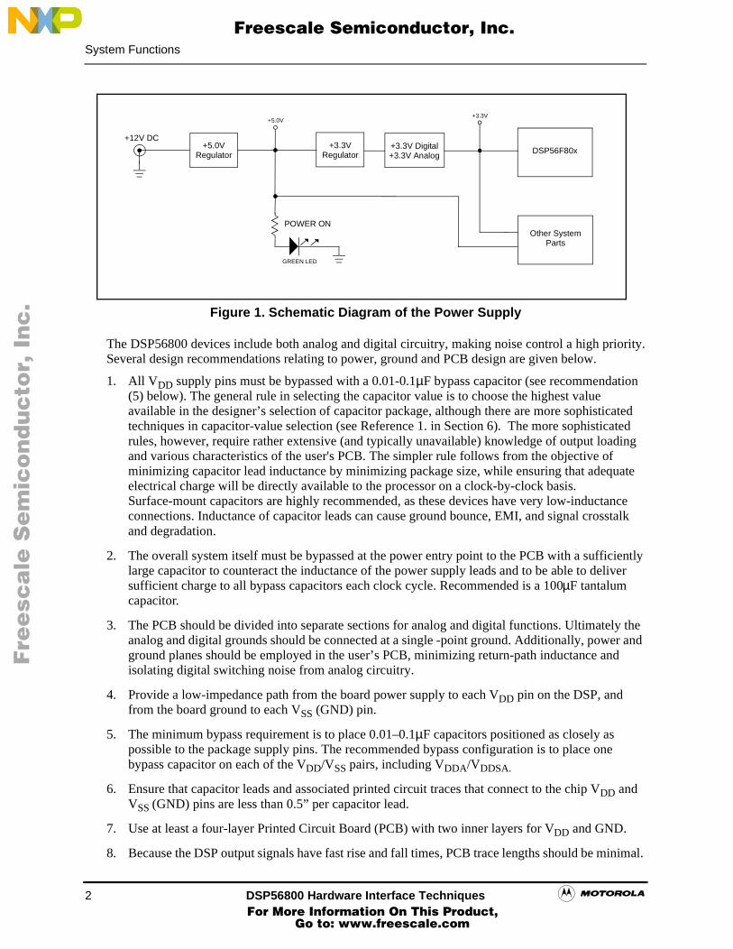
An example power supply circuit is given in Figure 1.
Contents
1. Introduction ....................................1
2. System Functions ...........................12.1 Providing Supply Voltage to the
DSP56800........................................12.2 Providing Clock to the DSP56800 ..32.3 Power Management.........................42.4 Reset/Interrupt Interfaces ................72.5 JTAG/OnCE Interface.....................9
3. Memory Interfaces .......................113.1 DSP56F800 Memory
Configuration.................................113.2 External Memory Interfaces..........14
4. Peripheral Interfaces ....................184.1 GPIO Interface Example ...............184.2 CAN Interface (DSP56F805)........184.3 Codec Interface (DSP56824) ........194.4 PWM Interface ..............................214.5 Motor Protection Logic .................224.6 SCI Interface .................................244.7 Quadrature Decoder Interface .......254.8 Zero-Crossing Detection ...............25
5. Conclusion ................................... 25
6. References ....................................26
Fre
esc
ale
Se
mic
on
du
cto
r, I
Freescale Semiconductor, Inc.
For More Information On This Product, Go to: www.freescale.com
nc
...
2 DSP56800 Hardware Interface Techniques
System Functions
Figure 1. Schematic Diagram of the Power Supply
The DSP56800 devices include both analog and digital circuitry, making noise control a high priority.Several design recommendations relating to power, ground and PCB design are given below.
1. All VDD supply pins must be bypassed with a 0.01-0.1µF bypass capacitor (see recommendation (5) below). The general rule in selecting the capacitor value is to choose the highest value available in the designer’s selection of capacitor package, although there are more sophisticated techniques in capacitor-value selection (see Reference 1. in Section 6). The more sophisticated rules, however, require rather extensive (and typically unavailable) knowledge of output loading and various characteristics of the user's PCB. The simpler rule follows from the objective of minimizing capacitor lead inductance by minimizing package size, while ensuring that adequate electrical charge will be directly available to the processor on a clock-by-clock basis. Surface-mount capacitors are highly recommended, as these devices have very low-inductance connections. Inductance of capacitor leads can cause ground bounce, EMI, and signal crosstalk and degradation.
2. The overall system itself must be bypassed at the power entry point to the PCB with a sufficiently large capacitor to counteract the inductance of the power supply leads and to be able to deliver sufficient charge to all bypass capacitors each clock cycle. Recommended is a 100µF tantalum capacitor.
3. The PCB should be divided into separate sections for analog and digital functions. Ultimately the analog and digital grounds should be connected at a single -point ground. Additionally, power and ground planes should be employed in the user’s PCB, minimizing return-path inductance and isolating digital switching noise from analog circuitry.
4. Provide a low-impedance path from the board power supply to each VDD pin on the DSP, and from the board ground to each VSS (GND) pin.
5. The minimum bypass requirement is to place 0.01–0.1µF capacitors positioned as closely as possible to the package supply pins. The recommended bypass configuration is to place one bypass capacitor on each of the VDD/VSS pairs, including VDDA/VDDSA.
6. Ensure that capacitor leads and associated printed circuit traces that connect to the chip VDD and VSS (GND) pins are less than 0.5” per capacitor lead.
7. Use at least a four-layer Printed Circuit Board (PCB) with two inner layers for VDD and GND.
8. Because the DSP output signals have fast rise and fall times, PCB trace lengths should be minimal.
+12V DC+5.0V
Regulator
POWER ON
GREEN LED
+3.3VRegulator
+3.3V Digital+3.3V Analog
+5.0V+3.3V
DSP56F80x
Other SystemParts
Fre
esc
ale
Se
mic
on
du
cto
r, I
Freescale Semiconductor, Inc.
For More Information On This Product, Go to: www.freescale.com
nc
...

System Functions
DSP56800 Hardware Interface Techniques 3
9. Consider all device loads as well as parasitic capacitance due to PCB traces when calculating capacitance. This is especially critical in systems with higher capacitive loads that could create higher transient currents in the VDD and GND circuits.
10. All inputs must be terminated (i.e., not allowed to float) using CMOS levels.
11. Take special care to minimize noise levels on the VREF, VDDA and VSSA pins.
2.2 Providing Clock to the DSP56800The DSP56F80x system clock can be derived from a crystal or an external system clock signal. Togenerate a reference frequency using the internal oscillator, a reference crystal must be connectedbetween the EXTAL and XTAL pins. For the DSP56801 (only), an additional clock option isavailable, which is the use of an internal relaxation oscillator which requires no external circuitrywhatsoever.
2.2.1 Crystal Oscillator
The internal oscillator is also designed to interface with a parallel-resonant crystal resonator in thefrequency range specified for the external crystal in Table 1. In Figure 2, a typical crystal oscillatorcircuit is shown. Follow the crystal supplier’s recommendations when selecting a crystal, becausecrystal parameters determine the component values required to provide maximum stability and reliablestart-up. The load capacitance values used in the oscillator circuit design should include all stray layoutcapacitances. The crystal and associated components should be mounted as closely as possible to theEXTAL and XTAL pins to minimize output distortion and start-up stabilization time.
Table 1: PLL TimingOperating Conditions: VSS = VSSA = 0 V, VDD = VDDA = 3.0–3.6 V, TA = –40° to +85°C
Figure 2. Crystal Oscillator
Characteristic Symbol Min Typ Max Unit
External reference crystal frequency for the PLL1
1 An externally supplied reference clock should be as free as possible from any phase jitter for the PLL to work correctly. The PLL is optimized for 8 MHz input crystal.
fosc 4 8 8 MHz
PLL output frequency fop 40 — 80 MHz
PLL stabilization time 2
2 This is the minimum time required after the PLL setup is changed to ensure reliable operation.
tplls — 1 10 ms
Sample External Crystal Parameters:Rz = 10 MΩ
Crystal Frequency = 4–8 MHz (optimized for 8 MHz)
EXTAL XTALRz
Fre
esc
ale
Se
mic
on
du
cto
r, I
Freescale Semiconductor, Inc.
For More Information On This Product, Go to: www.freescale.com
nc
...

4 DSP56800 Hardware Interface Techniques
System Functions
2.2.2 External Clock Source
The recommended method of connecting an external clock is given in Figure 3. The external clocksource is connected to XTAL and the EXTAL pin is grounded.
Figure 3. Connecting an External Clock Signal using XTAL
It is possible to instead drive EXTAL with an external clock, though this is not the recommendedmethod. If you elect to drive EXTAL with an external clock source, the following conditions must bemet:
1. XTAL must be completely unloaded
2. The maximum frequency of the applied clock must be less than 8MHz
Figure 4 illustrates how to connect an external clock circuit with a external clock source usingEXTAL as the input.
Figure 4. Connecting an External Clock Signal using EXTAL
2.3 Power ManagementThe DSP56F80x power requirement depends on several factors, including mode of operation(ACTIVE, STOP or WAIT), and system-level parameters including supply voltage, clock frequency,operating temperature and output loading. Careful consideration of each of these factors can result in asupply current requirement significantly less that the maximum found in the device ElectricalSpecification. In the following sub-sections, plots are shown that apply only to the DSP56F805. Theseare intended to show behavior of the device current requirement and do not supersede the deviceElectrical Specification.
2.3.1 Device ModelThe DSP56800 total current requirement (Itotal) is given by:
Itotal = Idigital + Ianalog
Idigital is given by:
Idigital = C*VDD*f
DSP56F805
XTAL EXTAL
External GNDClock
DSP56F805
XTAL EXTAL
No ExternalConnection Clock ( < 8MHz)
Fre
esc
ale
Se
mic
on
du
cto
r, I
Freescale Semiconductor, Inc.
For More Information On This Product, Go to: www.freescale.com
nc
...

System Functions
DSP56800 Hardware Interface Techniques 5
where C depends on die area and output capacitive loading as described below, VDD is the digitalsupply voltage, and f is the operating frequency of the device. This results from a total capacitance Cbeing charged every T seconds, where T is the machine cycle time. The charge required from thepower supply for each cycle T is Q = C * VDD. Hence Idigital = Q/T = C * VDD * f. Further, Idigitalvaries with temperature as described in subsequent sections.
Ianalog depends on output loading and other factors as described below.
2.3.2 Mode of Operation
The DSP56800 devices support two low-power modes, referred to as STOP and WAIT modes. Theseare described in detail in the associated device User Manuals, and the resulting reductions in supplycurrent requirement are given in the device Electrical Specifications. Both modes put the CPU to sleep.The PLL and peripheral bus continue to run in WAIT mode, but not in STOP mode. The ADC isplaced in a low-power mode in both cases.
2.3.3 Variation with Respect to Supply Voltage
The digital supply current requirement of CMOS devices with respect to supply voltage isapproximately linear, as shown in Figure 5. below for the DSP56805. The DSP56800 devices possessboth a CMOS current requirement and an analog current requirement. The variation of analog supplycurrent with respect to analog supply voltage is shown in Figure 6. These curves are consistent withthe model described in Section 2.3.1.
Figure 5. Total IDD vs. VDD
Total IDD vs VDD (nom Temp, 80 MHz PLL)
72
74
76
78
80
82
84
86
88
90
92
VDD min VDD nom VDD max
VDD
Fre
esc
ale
Se
mic
on
du
cto
r, I
Freescale Semiconductor, Inc.
For More Information On This Product, Go to: www.freescale.com
nc
...

6 DSP56800 Hardware Interface Techniques
System Functions
Figure 6. IDDA vs. VDDA
2.3.4 Variation with Respect to Operating FrequencyThe digital supply current requirement of CMOS devices with respect to frequency is approximatelylinear, as shown in Figure 7 below. These curves are consistent with the device current model.
Figure 7. IDD vs. PLL Frequency
IDDA vs. VDDA (nom Temp, 80 MHz PLL)
52
52.5
53
53.5
54
54.5
55
55.5
VDDA min VDDA nom VDDA max
VDDA
IDD vs. PLL Frequency
0
20
40
60
80
100
120
0 MHz 20 Mhz 40 Mhz 60 Mhz 80 Mhz
PLL Frequency
Analog IDD typical
Analog IDD max
IO IDD max
IO IDD typical
Fre
esc
ale
Se
mic
on
du
cto
r, I
Freescale Semiconductor, Inc.
For More Information On This Product, Go to: www.freescale.com
nc
...
System Functions
DSP56800 Hardware Interface Techniques 7
2.3.5 Variation with Respect to Output Loading
Output loading influences supply current requirement in a manner similar to that described by themodel given in Section 2.3.1. Output load current for a given output pin is the sum of DC and ACcurrents. The DC current requirement is that imposed by connected devices, such as TTL inputs. TheAC component is essentially a time-averaged capacitor charging current, which is dependent on VDD,capacitance and switching frequency. The capacitance in this case is the sum of DSP56800 outputbuffer capacitance, input capacitances of connected CMOS or other devices, and trace and straycapacitances.
2.3.6 Power Dissipation
Minimization of power dissipation of the DSP56800 device is a slightly different problem than that ofminimizing the device’s supply current requirement. The chief difference lies in the way the I/O pinsof the device are exercised. For example, when a DSP56800 digital I/O pin sinks current, the internalenergy generated must be dissipated as heat, although literally this does not affect the DSP56800’scurrent requirement, because this current does not enter the device through its VDD pins.
The specification of power dissipation for a given DSP56800 device is given in the corresponding datasheet.
2.4 Reset/Interrupt Interfaces
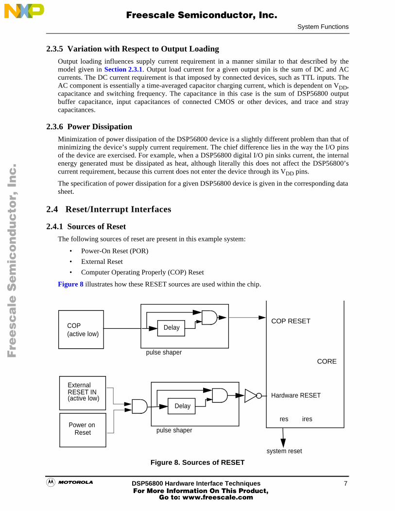
2.4.1 Sources of ResetThe following sources of reset are present in this example system:
• Power-On Reset (POR)
• External Reset
• Computer Operating Properly (COP) Reset
Figure 8 illustrates how these RESET sources are used within the chip.
Figure 8. Sources of RESET
Hardware RESET
COP RESET
CORE
COP
ExternalRESET IN
res ires
Delay
pulse shaper
Delay
pulse shaper
(active low)
(active low)
system reset
Power on Reset
Fre
esc
ale
Se
mic
on
du
cto
r, I
Freescale Semiconductor, Inc.
For More Information On This Product, Go to: www.freescale.com
nc
...

8 DSP56800 Hardware Interface Techniques
System Functions
By default, the pulse shaper functions force internal reset signals to be a minimum of 32 oscillatorclock cycles long. 38T (where T = 1/2 cycle) is required for the DSP56800 core and 1µs is required forrecovery time for the embedded flash. So, 32 works out to be a convenient value (assuming 8MHzoscillator frequency).
In addition to the reset sources above, two low-voltage detect signals may be used to initiate acontrolled shutdown of the chip when the supply drops below acceptable levels. These low-voltagedetect circuits are set up as high-priority interrupts. They can be masked if desired. See Chapter 16 inthe DSP56F80x User’s Manual.
Logic is provided on the DSP56800 to generate a clean power-on RESET signal. An example RESETcircuit is shown in Figure 9.
Figure 9. Schematic Diagram of the RESET Interface
2.4.2 External Interrupt Pin Interface
Figure 10 shows an example hardware interface to the external interrupt pins IRQA and IRQB.
Figure 10. Schematic Diagram of the External Interrupt Pin Interface
RESETPUSHBUTTON
MANUAL RESET
P_RESET
RESET
+3.3V
DSP56F807
IRQA
IRQB
+3.3V
+3.3V
10K
10K
SW2
SW3
0.1µF
0.1µF
Fre
esc
ale
Se
mic
on
du
cto
r, I
Freescale Semiconductor, Inc.
For More Information On This Product, Go to: www.freescale.com
nc
...
System Functions
DSP56800 Hardware Interface Techniques 9
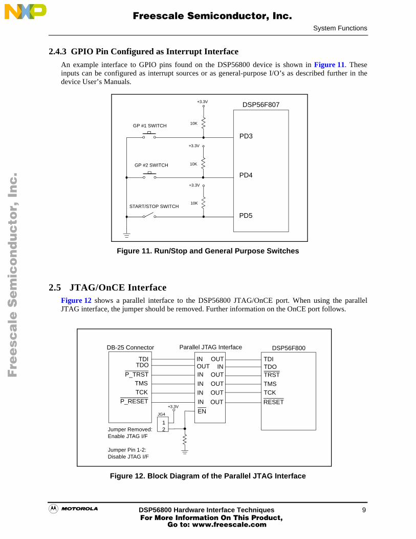
2.4.3 GPIO Pin Configured as Interrupt Interface
An example interface to GPIO pins found on the DSP56800 device is shown in Figure 11. Theseinputs can be configured as interrupt sources or as general-purpose I/O’s as described further in thedevice User’s Manuals.
Figure 11. Run/Stop and General Purpose Switches
2.5 JTAG/OnCE InterfaceFigure 12 shows a parallel interface to the DSP56800 JTAG/OnCE port. When using the parallelJTAG interface, the jumper should be removed. Further information on the OnCE port follows.
Figure 12. Block Diagram of the Parallel JTAG Interface
DSP56F807+3.3V
PD3
PD4
PD5
+3.3V
10K
10K
10K
GP #1 SWITCH
GP #2 SWITCH
START/STOP SWITCH
+3.3V
DB-25 Connector Parallel JTAG Interface DSP56F800
TDITDO
P_TRSTTMS
TCK
P_RESET
OUTOUT
OUT
OUT
OUT
OUTIN
ININ
IN
IN
IN
EN
TDITDOTRST
TMSTCK
RESET
JG4
12
+3.3V
Jumper Removed:Enable JTAG I/F
Jumper Pin 1-2:Disable JTAG I/F
Fre
esc
ale
Se
mic
on
du
cto
r, I
Freescale Semiconductor, Inc.
For More Information On This Product, Go to: www.freescale.com
nc
...
10 DSP56800 Hardware Interface Techniques
System Functions
This section is dedicated to testing and debugging retention, but specifically through the Joint TestAction Group, (JTAG) and the OnCE module.
DSP56F801/803/805/807 provides board and chip-level testing capability through two on-chipmodules, both accessed through the JTAG port/OnCE module interface:
• On-chip Emulation (OnCE) module
• Test Access Port (TAP) and 16-state controller, also known as the Joint Test Action Group (JTAG) port
Presence of the JTAG port/OnCE module interface permits insertion of the DSP chip into a targetsystem while retaining debug control. This capability is especially important for devices without anexternal bus, because it eliminates the need for a costly cable to bring out the footprint of the chiprequired by a traditional emulator system.
The OnCE module is a Freescale-designed module used in Digital Signal Processor (DSP) chips todebug application software employed with the chip. The port is a separate on-chip block allowingnon-intrusive DSP interaction with accessibility through the pins of the JTAG interface. The OnCEmodule makes it possible to examine registers, memory, or on-chip peripherals’ contents in a specialdebug environment. This avoids sacrificing any user-accessible on-chip resources to performdebugging. See Chapter 17, OnCE Module, in the DSP56F80x User’s Manual for details on theOnCE module implementation of the DSP56F801,803, 805 and 807 series.
The JTAG port is a dedicated user-accessible TAP compatible with the IEEE 1149.1a-1993 StandardTest Access Port and Boundary Scan Architecture. Problems associated with testing high-densitycircuit boards have led to the development of this proposed standard under the sponsorship of the TestTechnology Committee of IEEE and the JTAG. DSP56F 801 through 807 supports circuit board teststrategies based on this standard.
Five dedicated pins interface to the TAP containing a 16-state controller. The TAP uses a boundaryscan technique to test the interconnections between integrated circuits after they are assembled onto aPrinted Circuit Board (PCB). Boundary scans allow a tester to observe and control signal levels ateach component pin through a shift register placed next to each pin. This is important for testingcontinuity and determining if pins are stuck at a one or zero level.
Features of the TAP port include the following:
• Perform boundary scan operations to test circuit board electrical continuity
• Bypass the DSP for a given circuit board test by replacing the Boundary Scan Register (BSR) with a single-bit register
• Sample the DSP system pins during operation and transparently shift out the result in the CSR; pre-load values to output pins prior to invoking the EXTEST instruction
• Disable the output drive to pins during circuit board testing
• Provide a means of accessing the OnCE module controller and circuits to control a target system
• Query identification information, manufacturer, pat number, and version from a DSP chip
• Force test data onto the outputs of a DSP IC while replacing its BSR in the serial data path with a single bit register
• Enable a weak pull-up current device on all input signals of a DSP IC, helping to assure deterministic test results in the presence of continuity fault during interconnect testing
Fre
esc
ale
Se
mic
on
du
cto
r, I
Freescale Semiconductor, Inc.
For More Information On This Product, Go to: www.freescale.com
nc
...
Memory Interfaces
DSP56800 Hardware Interface Techniques 11
This section includes aspects of the JTAG implementation specific to the DSP56F801 through 807.This data is intended to be utilized with IEEE 1149.1a. The discussion includes those items requiredby the standard to be defined and, in certain cases, provides additional information specific to theDSP56F801/803/805/807. For internal details and applications of the standard, refer to IEEE 1149.1a.
3. Memory InterfacesMemory configuration is controlled slightly differently for the DSP56800 and DSP5682x devices asdescribed below. From a hardware perspective, the DSP56800 device memory map is controlled by asingle pin (EXTBOOT), while for DSP5682x devices, the MODA and MODB pins control thememory configuration.
3.1 DSP56F800 Memory ConfigurationThe DSP56800 chips have two valid operating modes determining the memory maps for programmemory. Operating modes can be selected either by applying the appropriate signal to the EXTBOOTpin during reset, or by writing to the Operating Mode Register (OMR) and changing the MA and MBbits.
The EXTBOOT pin is sampled as the chip leaves the reset state, and the initial operating mode of thechip is set accordingly.
Chip operating modes can also be changed by writing to the operating mode bits MB and MA in theOMR. Changing operating modes does not reset the chip. Interrupts should be disabled immediatelybefore changing the OMR. This will prevent an interrupt from going to the wrong memory location.Also, one No-Operation (NOP) instruction should be included after changing the OMR to allow forre-mapping to occur.
Note: Upon Computer Operating Properly (COP) reset, the MA and MB bits will revert to the values originally latched from the EXTBOOT pin in contradiction of RESET, hardware reset. These original mode values determine the COP reset vector.
3.1.1 Single Chip Mode: Start-up (Mode 0)
Mode zero is the single-chip mode. Internal Program RAM (PRAM) and PFLASH are enabled forreads and fetches. The DSP56xxx have two sub-modes for:
1. Mode 0A, boot mode, where all memory is internal
2. Mode 0B, non-boot mode, where the first 32K of memory is internal and the second 32K is external
Table 2: DSP56800 Program Memory Chip Operating Modes
State of EXTBOOT upon reset MB MA Chip operating mode
0 0 0 Mode 0NORMAL Operation
N/A 0 1 NOT SUPPORTED
N/A 1 0
1 1 1 Mode 3EXTERNAL ROM
Fre
esc
ale
Se
mic
on
du
cto
r, I
Freescale Semiconductor, Inc.
For More Information On This Product, Go to: www.freescale.com
nc
...

12 DSP56800 Hardware Interface Techniques
Memory Interfaces
If EXTBOOT is asserted low during reset, then Mode 0A: boot is automatically entered when exitingReset mode.
For DSP56F801, Mode0B is not supported because there is no external memory interface.
Note: Locations zero through three in the program memory space are actually mapped to the first four locations in the Boot Flash.
Mode zero is useful to enter when coming out of reset for applications while executing primarily frominternal program memory. The reset vector location in Modes zero and three is located in the programmemory space at location P:$0000, P:$0002 for COP timer reset. For Mode zero, this is in internalprogram memory. In Mode three, it is in off-chip program memory.
3.1.2 Modes 1 & 2
Modes one and two are NOT SUPPORTED for these parts. They are used for ROM-based members ofthe DSP56800 family.
3.1.3 External Mode (Mode 3) Mode three is a development mode in which the entire 64K program memory space is external. Nointernal program memory may be accessed, except as a secondary read of Data RAM. The reset vectorlocation in Mode three is located in the external program memory space at location P:$0000, P:$0002for COP timer reset.
3.1.4 DSP56824 Memory Configuration
The DSP56824 has four operating modes that determine the memory maps for program and datamemories and the startup procedure when the chip leaves the Reset state. Operating modes can beselected either by applying the appropriate signals to the MODA and MODB pins during reset, or bywriting to the OMR and changing the MA and MB bits, as shown in Table 2.
.
Table 3: DSP56824 Program RAM Chip Operating Modes
MB orMODBValue
MA orMODAValue
Chip Operating
ModeReset Vector
Program Memory Configuration
P:$7F–$0 P:$8000–$80
0 0 Mode 0Single ChipStartup
Internal program ROM P:$0000 or P:$0002 (COP reset)
Read/fetch: internal pro-gram ROM Write: internal program RAM
All accesses: internal program ROM
0 1 Mode 1Single Chip User
Internal program ROM P:$7F80 or P:$7F82 (COP reset)
All accesses: internal pro-gram RAM
All accesses: internal program ROM
1 0 Mode 2Normal Expanded
External program memory P:$E000 or P:$E002 (COP reset)
Read/fetch: internal pro-gram ROM Write: internal program RAM
All accesses: internal program ROM
1 1 Mode 3Development
External program memory P:$0000 or P:$0002 (COP reset)
All accesses: externalprogram memory
All accesses: external pro-gram memory
Fre
esc
ale
Se
mic
on
du
cto
r, I
Freescale Semiconductor, Inc.
For More Information On This Product, Go to: www.freescale.com
nc
...
Memory Interfaces
DSP56800 Hardware Interface Techniques 13
The MODA and MODB pins are sampled as the DSP56824 leaves the Reset state, and the initialoperating mode of the chip is set accordingly. After the Reset state is exited, the MODA and MODBpins become interrupt pins, IRQA and IRQB. One of four initial operating modes is selected, based onthe values detected on MODA and MODB:
• Single Chip mode (Mode 0 or Mode 1)
• Normal Expanded mode (Mode 2)
• Development mode (Mode 3)
Chip operating modes can also be changed by writing to the MB and MA bits in the OMR. Changingoperating modes does not reset the DSP56824. To prevent an interrupt from going to the wrongmemory location, interrupts should be disabled immediately before changing the OMR. Also, oneno-operation (NOP) instruction should be included after changing the OMR to allow for remapping tooccur.
Note: On a Computer Operating Properly (COP) reset, the MA and MB bits (in the OMR) revert to the values originally latched from the MODA and MODB pins on deassertion of RESET. These values determine the COP reset vector. For example, if the DSP56xxx left hardware reset in Mode 2 and the mode bits in the OMR were later changed to specify Mode 3, a COP reset would use reset vector P:$E002 (for Mode 2) for its reset vector, and not P:$0002 (for Mode 3).
3.1.5 Single Chip Bootstrap Mode (Mode 0) Mode 0 is the Single Chip bootstrap mode in which all the internal program and data memory space isenabled; see Table 3. Mode 0 can be entered by either pulling the MODA and MODB pins low beforeresetting the chip or by writing to the OMR and clearing the MA and MB bits. Writes to the lower 128words of internal program space will write to the internal program RAM. The reset vector location inMode 0 is P:$0000 in the internal program ROM (P:$0002 for COP timer reset).
Mode 0 is useful when exiting the Reset state for applications that execute primarily from internalprogram ROM. Write access to the internal program RAM allows an application to copy interruptvectors and program code from program ROM to identically addressed locations in program RAMwithout changing operating modes.
3.1.6 Single Chip User (Mode 1)
Mode 1 is the Single Chip user mode in which 34,640 (32,768 – 128) words of internal program ROMare enabled for reads and fetches. All accesses to the lower 128 words of internal program space are tothe internal program RAM. The reset vector location in Mode 1 is P:$7F80 in the internal programROM (P:$7F82 for COP timer reset). The user should observe that these reset vectors are located in thearea reserved for the bootstrap program.
Mode 1 is the ordinary user mode for applications that execute primarily from internal program ROMor for applications that must access the internal program RAM. The internal program RAM is typicallyloaded in Mode 0 or by the bootstrap program in Mode 1. For more information on loading the internalprogram RAM in this manner, see Appendix A, “Bootstrap Program” , in the DSP56824 User’sManual.
Fre
esc
ale
Se
mic
on
du
cto
r, I
Freescale Semiconductor, Inc.
For More Information On This Product, Go to: www.freescale.com
nc
...

14 DSP56800 Hardware Interface Techniques
Memory Interfaces
3.1.7 Normal Expanded Mode (Mode 2)
In the Normal Expanded mode (Mode 2), all 32,768 words of internal program ROM are enabled forreads and fetches. Writes to the lower 128 words of internal program space will write to the internalprogram RAM. The reset vector location in Mode 2 is at P:$E000 in the external program RAM(P:$E002 for COP timer reset).
Mode 2 is identical to Mode 0 except that the reset vectors are in external memory. This featureprovides additional flexibility for application development.
3.1.8 Development Mode (Mode 3)
Mode 3 is the Development mode, in which the entire 65,536 words of program memory space isexternal. No internal program memory space can be accessed. The reset vector location in Mode 3 is atP:$0000 in the external program memory space (P:$0002 for COP timer reset). Mode 3 is the primarymode for application development on the DSP56824.
3.2 External Memory InterfacesThe DSP56800 family devices (excluding the DSP56801) have an external 16-bit multiplexed data busthat can be used for program word or data accesses to memory devices, including ROM, FLASH,EEPROM, or SRAM. The PS and DS outputs from the DSP device differentiate the two types ofaccesses. External bus accesses are referred to as asynchronous, as the timing specifications given inthe appropriate Electrical Specifications for each device are not made with respect to the DSP clock.
3.2.1 Wait State Management for the DSP56800
Optimization of external memory use, particularly for DSP56800 devices, depends on several factorsthat can be taken into consideration for a given hardware design.
First, as much internal memory as possible for a given application should be used, as all internalaccesses require zero wait states.
Second, if external memory must be used, partitioning the total code into two pieces can be beneficial.These two pieces are i) often used and repeated code, and ii) code used or needed less frequently.
Third, wait states (WS) are programmable for the values 0, 4, 8 and 12. Wait states have traditionallyprovided a means for accessing slower memories motivated either by technology limitations or to thecost advantage offered by slower memory devices. Each wait state extends external bus accesses by2*WS clock periods. Note that wait state values are independently programmable for external X (data)memory and external program memory. For example, the clock period (Top) for a device running at80MHz (CPU clock of 40MHz) is 12.5ns. External memory access time is given by :
tACC = Top*WS + (Top-11.5) (ns)
For example, 4 wait states for a CPU running at 40MHz (clock rate of 80MHz) results in a memoryaccess time of 12.5*4 + (12.5-11.5) = 51ns.
Many modern memory devices, such as SRAMs, cannot operate with 0 wait states but can, however,be accessed in the sub-10ns range. Therefore, for certain applications, it is worthwhile to considerselecting a lower clock frequency in order to be able to access external memory with no wait states.This is particularly true of applications that must make heavy use of external memory and isexemplified by the following:
Suppose an application requires only 25MIPS, rather than the maximum of 40MIPS.
Fre
esc
ale
Se
mic
on
du
cto
r, I
Freescale Semiconductor, Inc.
For More Information On This Product, Go to: www.freescale.com
nc
...

Memory Interfaces
DSP56800 Hardware Interface Techniques 15
Then:
Top = 1/50e6 = 20nsWS = 0
tACC = Top*0 + (Top – 11.5) = 8.5ns
Many SRAM devices are available in this speed range.
3.2.2 Program and Data Memory Example InterfaceThe DSP56807 EVM uses one bank of 128K×16-bit Fast Static RAM (GSI GS72116, labelled U2) forexternal memory expansion; see the FSRAM schematic diagram in Figure 13. This physical memorybank is split into two logical memory banks of 64Kx16-bits: one for program memory and the other fordata memory. By using the DSP’s program strobe, PS, signal line along with the memory chip’s A0signal line, half of the memory chip is selected when program memory accesses are requested and theother half of the memory chip is selected when data memory access are requested. This memory bankwill operate with zero wait state accesses while the DSP56F807 is running at 70MHz. However, whenrunning at 80MHz, the memory bank operates with four wait state accesses.
Figure 13. Schematic Diagram of the External Memory Interface
3.2.3 Memory Expansion Techniques
The total memory space addressable by the DSP56800 device is 64K words for program memory, plus64K words for data memory. However, paging techniques can be implemented in hardware as shownin the following two examples. The application developer must take appropriate steps in softwaredevelopment to accommodate page boundary transitions.
DSP56F807 GS72116
A0-A15
PS
D0-D15
RD
WR
A1-A16
A0
DQ0-DQ15
OE
WE
CE
+3.3V
JG1
Fre
esc
ale
Se
mic
on
du
cto
r, I
Freescale Semiconductor, Inc.
For More Information On This Product, Go to: www.freescale.com
nc
...

16 DSP56800 Hardware Interface Techniques
Memory Interfaces
3.2.3.1 Memory Paging Using GPIO
Figure 14 below shows a simple technique to select different banks of memory. A given bank ofmemory is enabled by setting the appropriate GPIO pin to zero. Note that only one bank of memorycan be enabled at any given time. Therefore, the programmer must manage the GPIO pins carefully,allowing only one pin to be set low in the expanded memory system. Pseudocode for using thistechnique is given as follows.
Initialize GPIO pin control registers
For a page transition (indicated by software monitoring or by an interrupt handler):
i) Jump to internal program memory
ii) Modify GPIO control registers as appropriate
iii) Jump to the new external page
Figure 14. Expansion Memory Example Using GPIO
3.2.3.2 Memory Paging Using Latched Data as Address
Figure 15 shows a second way to page external memory. This technique multiplies the address space to8 times 64K words = 512K words of both program and data space. Each memory bank is selected byan output from the ‘138 decoder. The decoder’s inputs are driven from 3 outputs of a 4-bit latch, fed by3 data lines from the DSP56800 device. A dedicated GPIO pin controls the clock to the latch. Whenthe GPIO pin is set high, the latch cannot be written. To execute a page transition, the GPIO pin mustbe set low via software control, followed by an external data write to the latch. The page must then belocked in in software by setting the GPIO pin back to one. Further, the GPIO pin can be used inconjuction with other logic to disable writing of any other external devices during a page transition.The following summarizes the steps required in software to use this technique.
DSP56F807 GS72116
A0-A15
PS
D0-D15
RD
WR
A1-A16
A0
DQ0-DQ15
OE
WE
CE
+3.3V
2.5K
GPIOBn
Fre
esc
ale
Se
mic
on
du
cto
r, I
Freescale Semiconductor, Inc.
For More Information On This Product, Go to: www.freescale.com
nc
...

Memory Interfaces
DSP56800 Hardware Interface Techniques 17
Initialize GPIO control registers
For a page transition:
i) Set GPIO to zero
ii) Execute external write cycle to latch with 12 waitstates
iii) Set GPIO to one
Note that one address of each bank must be reserved, as the write cycle to the latch will also write thecorresponding address in the previously selected bank.
Figure 15. Expansion Memory
3 3
3-8 Decoder
74LS138
GS72116
GS72116
CE
CE
A0
A0
WRGPIOB0
PS
4-bit LatchD0-D2
DSP56F807
OE
Fre
esc
ale
Se
mic
on
du
cto
r, I
Freescale Semiconductor, Inc.
For More Information On This Product, Go to: www.freescale.com
nc
...

18 DSP56800 Hardware Interface Techniques
Peripheral Interfaces
4. Peripheral InterfacesThe following sections provide example interfaces to DSP56800 peripherals. The interfaces have beenimplemented and tested on Evaluation Module (EVM) hardware using various members of theDSP56800 family.
4.1 GPIO Interface ExampleAn example interface making use of the DSP56800 GPIO pins is given below. The GPIO pins arecontrollable via SDK driver routines. Refer to the SDK Programmer’s Guide for details.
Two general-purpose user pushbutton switches are connected to Port D GPIO signals GPIOB0 andGPIOB1. A Run/Stop toggle switch is connected to GPIO signal GPIOB2; see Figure 16.
Figure 16. Run/Stop and General Purpose Switches
4.2 CAN Interface (DSP56F805)The DSP56F805EVM board contains a CAN physical-layer interface chip that is attached to theMSCAN_RX and MSCAN_TX pins on the DSP56F805. The EVM board uses a Philips, PCA82C250,high speed, 1Mbps, physical layer interface chip. Due to the +5.0V operating voltage of the CAN chip,a pull-up to +5.0V is required to level shift the Transmit Data output line from the DSP56F805. Aprimary, J1, and a daisy-chain, J2, CAN connector are provided to allow easy daisy-chaining of CANdevices. CAN bus termination of 120 ohms can be provided by adding a jumper as shown. Refer toFigure 4 for the CAN connector signals and Figure 17 for a connection diagram.
DSP56F807+3.3V
GPIOB0+3.3V
10K
10K
10K
GP #1 SWITCH
GP #2 SWITCH
START/STOP SWITCH
+3.3VGPIOB1
GPIOB2
Fre
esc
ale
Se
mic
on
du
cto
r, I
Freescale Semiconductor, Inc.
For More Information On This Product, Go to: www.freescale.com
nc
...

Peripheral Interfaces
DSP56800 Hardware Interface Techniques 19
Figure 17. CAN Interface
4.3 Codec Interface (DSP56824)The DSP56824EVM provides a 13-bit linear single-channel CODEC (Freescale MC145483,designated as U10). The DSP56824 interfaces to the CODEC via the DSP’s Synchronous SerialInterface (SSI) through the SSI enable connector, J1. This connector allows the SSI Port to eithercontrol the on-board SSI CODEC or to control an off-board SSI device. Table 5 lists the J1 pin-outs.The SSI port provides the CODEC’s clock, frame synchronization and data without the use of gluelogic; see Figure 18.
Table 4: CAN Header Description
J1 and J2
Pin # Signal Pin # Signal
1 NC 2 NC
3 CANL 4 CANH
5 GND 6 NC
7 NC 8 NC
9 NC 10 NC
DSP56F805
MSCAN_TX
MSCAN_RX
CAN CONNECTOR
TXD
RXD
SLOPE
VREFVCC
GND
CANL
PCA82C250T
1357
2468
X
1
2120
CAN TERMINATION
CANH
J1
U201
4
8
+5.0V
35
2
DAISY-CHAINCAN CONNECTOR
76
X
X
X
XXX
1357
2468
X
J2X
X
X
XXX
Fre
esc
ale
Se
mic
on
du
cto
r, I
Freescale Semiconductor, Inc.
For More Information On This Product, Go to: www.freescale.com
nc
...

20 DSP56800 Hardware Interface Techniques
Peripheral Interfaces
Figure 18. Block Diagram of the SSI CODEC Interface
3.4 DAC Interface using SPI Port
The DSP56F807EVM board contains a serial 10-bit, 4-channel D/A converter connected to theDSP56F807’s SPI port. The output pins are uncommitted and are connected to a 4X2 header, J1, toallow easy user connections. Refer to Figure 19 for the D/A connections. The D/A’s output full-scalerange value can be set to a value from 0.0V to 2.4V by a trimpot, R1. This trimpot is preset to +2.05V,which provides approximately 2mV per step.
Table 5: SSI CODEC Enable Connector Descriptor
J1
Pin # DSP Signal Pin # CODEC Signal
1 STD/PC8 2 DR
3 SRD/PC9 4 DT
5 STCK/PC10 6 BCLKR/BCLKT/MCLK
7 STFS/PC11 8 FST/FSR
9 SRCK/PC12 10 NC
11 SRFS/PC13 12 NC
13 GND 14 GND
DSP56824 MC145483J1
CODEC Enable(SSI Port Connector)
SRD
STD
STCK
STFS
SRCK
SRFS
DR
DT
BCLKR, BCLKT, MCLK
FST, FSR
Fre
esc
ale
Se
mic
on
du
cto
r, I
Freescale Semiconductor, Inc.
For More Information On This Product, Go to: www.freescale.com
nc
...

Peripheral Interfaces
DSP56800 Hardware Interface Techniques 21
Figure 19. Serial 10-bit, 4-Channel D/A Converter
4.4 PWM InterfaceThe sections below describe example interfaces to the PWM module(s) available on DSP56800devices.
The DSP56F807 has two independent groups of dedicated PWM units. Each unit contains six PWM,three Phase Current sense and four Fault input lines. PWM group A’s PWM lines are connected to aUNI-3 interface connector and to a set of six PWM LEDs via inverting buffers. “UNI-3” refers to aFreescale-defined parallel interface. Typically, any parallel cable, such as a HDD cable, will satisfy therequirements of the DSP56800 device. The inverting buffers are used to isolate and drive the DSP’sPWM group A’s outputs to the PWM LEDs. The PWM LEDs indicate the status of PWM group Asignals, as shown in Figure 20.
Figure 20. PWM Group A Interface and LEDs
DSP56F807MAX5251 D/A CONNECTOR
MOSI
MISO
SCLK
PB4
RSTO
DIN
DOUT
SCLK
CS
CL
OUT A
OUT B
OUT C
OUT D
Vref
1
3
5
7
2
4
6
8
D/A 0
D/A 1
D/A 2
D/A 3
J1
+3.3VA10K
R1
DSP56F807
LEDBUFFER
UNI-3PWMA0PWMA1PWMA2PWMA3PWMA4PWMA5
PWMA0PWMA1PWMA2PWMA3PWMA4PWMA5
YELLOW LED
GREEN LED
GREEN LED
GREEN LED
YELLOW LED
YELLOW LED
+3.3V
PHASE A TOP
PHASE A BOTTOM
PHASE B TOP
PHASE B BOTTOM
PHASE C TOP
PHASE C BOTTOM
LED4
LED5
LED6
LED7
LED8
LED9
Fre
esc
ale
Se
mic
on
du
cto
r, I
Freescale Semiconductor, Inc.
For More Information On This Product, Go to: www.freescale.com
nc
...
22 DSP56800 Hardware Interface Techniques
Peripheral Interfaces
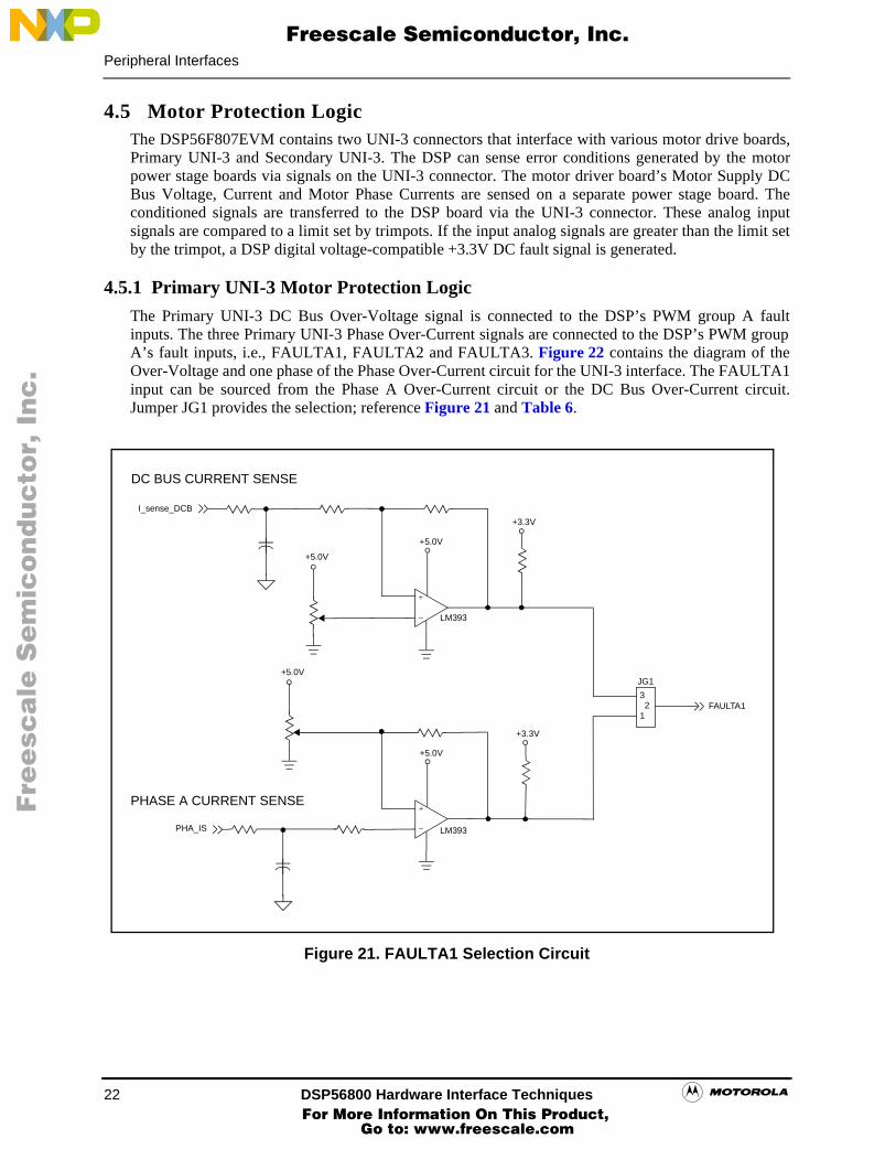
4.5 Motor Protection LogicThe DSP56F807EVM contains two UNI-3 connectors that interface with various motor drive boards,Primary UNI-3 and Secondary UNI-3. The DSP can sense error conditions generated by the motorpower stage boards via signals on the UNI-3 connector. The motor driver board’s Motor Supply DCBus Voltage, Current and Motor Phase Currents are sensed on a separate power stage board. Theconditioned signals are transferred to the DSP board via the UNI-3 connector. These analog inputsignals are compared to a limit set by trimpots. If the input analog signals are greater than the limit setby the trimpot, a DSP digital voltage-compatible +3.3V DC fault signal is generated.
4.5.1 Primary UNI-3 Motor Protection Logic
The Primary UNI-3 DC Bus Over-Voltage signal is connected to the DSP’s PWM group A faultinputs. The three Primary UNI-3 Phase Over-Current signals are connected to the DSP’s PWM groupA’s fault inputs, i.e., FAULTA1, FAULTA2 and FAULTA3. Figure 22 contains the diagram of theOver-Voltage and one phase of the Phase Over-Current circuit for the UNI-3 interface. The FAULTA1input can be sourced from the Phase A Over-Current circuit or the DC Bus Over-Current circuit.Jumper JG1 provides the selection; reference Figure 21 and Table 6.
Figure 21. FAULTA1 Selection Circuit
DC BUS CURRENT SENSE
I_sense_DCB
+
–
+5.0V
+5.0V
LM393
+3.3V
JG1
3 21
FAULTA1
+
–
+5.0V
+5.0V
+3.3V
PHA_IS
PHASE A CURRENT SENSE
LM393
Fre
esc
ale
Se
mic
on
du
cto
r, I
Freescale Semiconductor, Inc.
For More Information On This Product, Go to: www.freescale.com
nc
...
Peripheral Interfaces
DSP56800 Hardware Interface Techniques 23
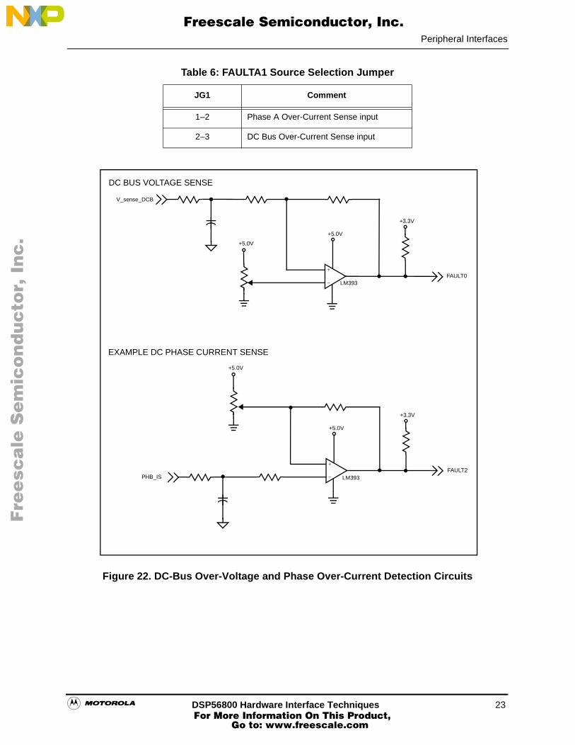
Figure 22. DC-Bus Over-Voltage and Phase Over-Current Detection Circuits
Table 6: FAULTA1 Source Selection Jumper
JG1 Comment
1–2 Phase A Over-Current Sense input
2–3 DC Bus Over-Current Sense input
+5.0V
+
–
+5.0V
+3.3V
V_sense_DCB
FAULT0LM393
+
–
+5.0V
+5.0V
+3.3V
FAULT2PHB_IS LM393
DC BUS VOLTAGE SENSE
EXAMPLE DC PHASE CURRENT SENSE
Fre
esc
ale
Se
mic
on
du
cto
r, I
Freescale Semiconductor, Inc.
For More Information On This Product, Go to: www.freescale.com
nc
...
24 DSP56800 Hardware Interface Techniques
Peripheral Interfaces
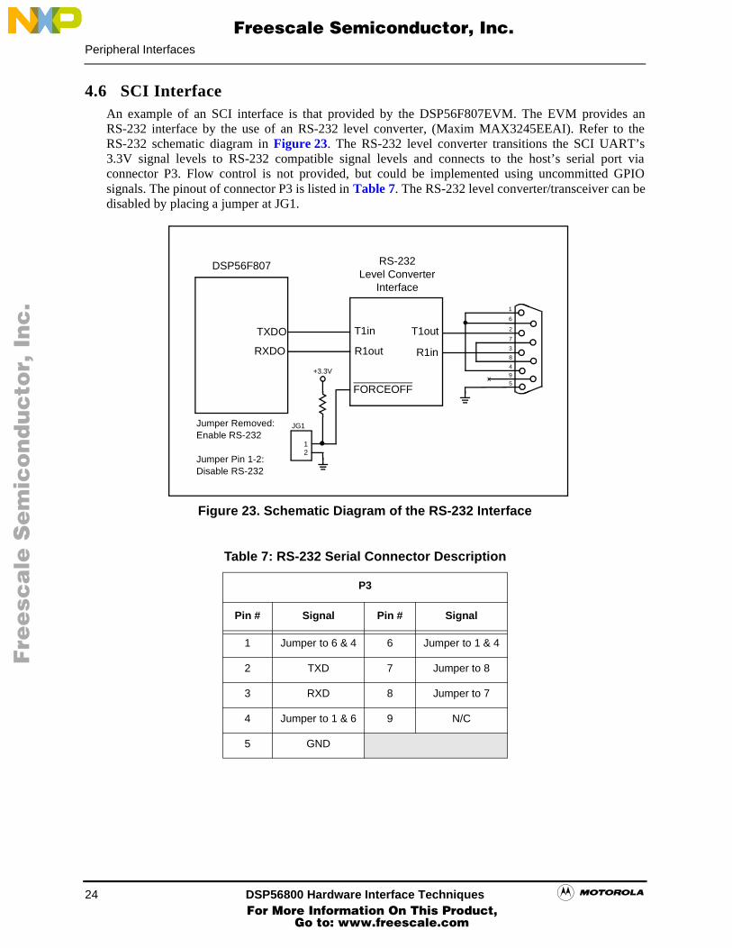
4.6 SCI InterfaceAn example of an SCI interface is that provided by the DSP56F807EVM. The EVM provides anRS-232 interface by the use of an RS-232 level converter, (Maxim MAX3245EEAI). Refer to theRS-232 schematic diagram in Figure 23. The RS-232 level converter transitions the SCI UART’s3.3V signal levels to RS-232 compatible signal levels and connects to the host’s serial port viaconnector P3. Flow control is not provided, but could be implemented using uncommitted GPIOsignals. The pinout of connector P3 is listed in Table 7. The RS-232 level converter/transceiver can bedisabled by placing a jumper at JG1.
Figure 23. Schematic Diagram of the RS-232 Interface
.
Table 7: RS-232 Serial Connector Description
P3
Pin # Signal Pin # Signal
1 Jumper to 6 & 4 6 Jumper to 1 & 4
2 TXD 7 Jumper to 8
3 RXD 8 Jumper to 7
4 Jumper to 1 & 6 9 N/C
5 GND
DSP56F807 RS-232Level Converter
Interface
TXDO
RXDO R1in
T1outT1in
R1out
FORCEOFF
JG1
12
6
3
2
7
8
4
5x
1
9+3.3V
Jumper Removed:Enable RS-232
Jumper Pin 1-2:Disable RS-232
Fre
esc
ale
Se
mic
on
du
cto
r, I
Freescale Semiconductor, Inc.
For More Information On This Product, Go to: www.freescale.com
nc
...
Conclusion
DSP56800 Hardware Interface Techniques 25
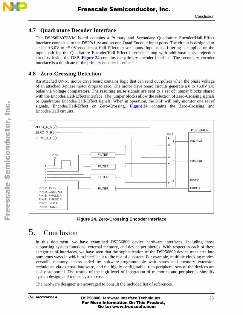
4.7 Quadrature Decoder InterfaceThe DSP56F807EVM board contains a Primary and Secondary Quadrature Encoder/Hall-Effectinterface connected to the DSP’s first and second Quad Encoder input ports. The circuit is designed toaccept +3.0V to +5.0V encoder or Hall-Effect sensor inputs. Input noise filtering is supplied on theinput path for the Quadrature Encoder/Hall-Effect interface, along with additional noise rejectioncircuitry inside the DSP. Figure 24 contains the primary encoder interface. The secondary encoderinterface is a duplicate of the primary encoder interface.
4.8 Zero-Crossing DetectionAn attached UNI-3 motor drive board contains logic that can send out pulses when the phase voltageof an attached 3-phase motor drops to zero. The motor drive board circuits generate a 0 to +5.0V DCpulse via voltage comparators. The resulting pulse signals are sent to a set of jumper blocks sharedwith the Encoder/Hall-Effect interface. The jumper blocks allow the selection of Zero-Crossing signalsor Quadrature Encoder/Hall-Effect signals. When in operation, the DSP will only monitor one set ofsignals, Encoder/Hall-Effect or Zero-Crossing. Figure 24 contains the Zero-Crossing andEncoder/Hall circuits.
Figure 24. Zero-Crossing Encoder Interface
5. ConclusionIn this document, we have examined DSP56800 device hardware interfaces, including thosesupporting system functions, external memory, and device peripherals. With respect to each of thesecategories of interfaces, we have seen that the sophistication of the DSP56800 device translates intonumerous ways in which to interface it to the rest of a system. For example, multiple clocking modes,versatile memory access aided by software-programmable wait states and memory extensiontechniques via external hardware, and the highly configurable, rich peripheral sets of the devices areeasily supported. The results of the high level of integration of memories and peripherals simplifysystem design, and reduce system cost.
The hardware designer is encouraged to consult the included list of references.
ZERO_X_A
ZERO_X_B
ZERO_X_C
123456
+5.0V FILTER
FILTER
FILTER
FILTERPIN 1: +5.0VPIN 2: GROUNDPIN 3: PHASE APIN 4: PHASE BPIN 5: INDEXPIN 6: HOME
12
3
45
6
7
89
JG12DSP56F807
PHASEA1
PHASEB1
INDEX1
HOME 1
Fre
esc
ale
Se
mic
on
du
cto
r, I
Freescale Semiconductor, Inc.
For More Information On This Product, Go to: www.freescale.com
nc
...

26 DSP56800 Hardware Interface Techniques
References
6. References1. Howard W. Johnson and Martin Graham, “High-Speed Digital Design”, PTR Prentice-Hall, 1993
2. DSP5680x User’s Manual, DSP56F801-7UM/D
3. DSP56824 User’s Manual, DSP56824UM/D
4. DSP56800 Family Manual, DSP56800FM/D
5. DSP56F803 Evaluation Module Hardware User’s Manual, DSP56F803
6. DSP56F805 Evaluation Module Hardware User’s Manual, DSP56F05EVMUM/D
7. DSP56F807 Evaluation Module Hardware User’s Manual, DSP56F807EVMUM/D
8. DSP56824 Evaluation Module Hardware Reference Manual, DSP56824EVMUM/D
9. Preliminary Technical Data DSP56F803 16-bit Digital Signal Processor, DSP56F803/D
10. Preliminary Technical Data DSP56F805 16-bit Digital Signal Processor, DSP56F805/D
11. Preliminary Technical Data DSP56F807 16-bit Digital Signal Processor, DSP56F807/D
12. Technical Data DSP56824 16-bit Digital Signal Processor, DSP56824/D
13. Embedded SDK Programmer’s Guide
Fre
esc
ale
Se
mic
on
du
cto
r, I
Freescale Semiconductor, Inc.
For More Information On This Product, Go to: www.freescale.com
nc
...

NOTES:
DSP56800 Hardware Interface Techniques 27
NOTES: _________________________________________________________________________________
_________________________________________________________________________________
_________________________________________________________________________________
_________________________________________________________________________________
_________________________________________________________________________________
_________________________________________________________________________________
_________________________________________________________________________________
_________________________________________________________________________________
_________________________________________________________________________________
_________________________________________________________________________________
_________________________________________________________________________________
_________________________________________________________________________________
_________________________________________________________________________________
_________________________________________________________________________________
_________________________________________________________________________________
_________________________________________________________________________________
_________________________________________________________________________________
_________________________________________________________________________________
_________________________________________________________________________________
_________________________________________________________________________________
_________________________________________________________________________________
_________________________________________________________________________________
_________________________________________________________________________________
_________________________________________________________________________________
_________________________________________________________________________________
_________________________________________________________________________________
_________________________________________________________________________________
_________________________________________________________________________________
_________________________________________________________________________________
_________________________________________________________________________________
_________________________________________________________________________________
_________________________________________________________________________________
_________________________________________________________________________________
_________________________________________________________________________________
Fre
esc
ale
Se
mic
on
du
cto
r, I
Freescale Semiconductor, Inc.
For More Information On This Product, Go to: www.freescale.com
nc
...

AN1920/D
Fre
esc
ale
Se
mic
on
du
cto
r, I
Freescale Semiconductor, Inc.
For More Information On This Product, Go to: www.freescale.com
nc
...
rxzb30
disclaimer
rxzb30
hibbertleft
rxzb30
freescalecolorjpeg