DEVELOPMENT OF A MICROCONTROLLER SYSTEM FOR A SENSOR NETWORK USED
Upload
duongkhanhCategory
view
218download
0
1 of 97
Note: Some revisions of this device may incorporate deviations from published specifications known as errata. Multiple revisions of any device may be simultaneously available through various sales channels. For information about device errata, click here: www.maxim-ic.com/errata.
GENERAL DESCRIPTION The DS80C400 network microcontroller offers the highest integration available in an 8051 device. Peripherals include a 10/100 Ethernet MAC, three serial ports, a CAN 2.0B controller, 1-Wire® Master, and 64 I/O pins.
To enable access to the network, a full application-accessible TCP IPv4/6 network stack and OS are provided in the ROM. The network stack supports up to 32 simultaneous TCP connections and can transfer up to 5Mbps through the Ethernet MAC. Its maximum system-clock frequency of 75MHz results in a minimum instruction cycle time of 54ns. Access to large program or data memory areas is simplified with a 24-bit addressing scheme that supports up to 16MB of contiguous memory.
To accelerate data transfers between the microcontroller and memory, the DS80C400 provides four data pointers, each of which can be configured to automatically increment or decrement upon execution of certain data pointer-related instructions. The DS80C400’s hardware math accelerator further increases the speed of 32-bit and 16-bit multiply and divide operations as well as high-speed shift, normalization, and accumulate functions.
The High-Speed Microcontroller User’s Guide and the High-Speed Microcontroller User’s Guide: Network Microcontroller Supplement should be used in conjunction with this data sheet. Download both at: www.maxim-ic.com/user_guides. APPLICATIONS Industrial Control/Automation Data Converters (Serial-
to-Ethernet, CAN-to-Ethernet) Environmental Monitoring
Network Sensors Remote Data Collection Equipment
Vending Transaction/Payment
Terminals Home/Office Automation
ORDERING INFORMATION PART TEMP RANGE PIN-PACKAGE
DS80C400-FNY -40°C to +85°C 100 LQFP
DS80C400-FNY+ -40°C to +85°C 100 LQFP +Denotes a lead(Pb)-free/RoHS-compliant package.
1-Wire is a registered trademark of Maxim Integrated Products, Inc. Magic Packet is a registered trademark of Advanced Micro Devices, Inc. DeviceNet is a trademark of Open DeviceNet Vendor Association, Inc.
FEATURES High-Performance Architecture
Single 8051 Instruction Cycle in 54ns DC to 75MHz Clock Rate Flat 16MB Address Space Four Data Pointers with Auto-Increment/
Decrement and Select-Accelerate Data Movement 16/32-Bit Math Accelerator
Multitiered Networking and I/O 10/100 Ethernet Media Access Controller (MAC) CAN 2.0B Controller 1-Wire Net Controller Three Full-Duplex Hardware Serial Ports Up to Eight Bidirectional 8-Bit Ports (64 Digital I/O
Pins) Robust ROM Firmware
Supports Network Boot Over Ethernet Using DHCP and TFTP
Full, Application-Accessible TCP/IP Network Stack Supports IPv4 and IPv6 Implements UDP, TCP, DHCP, ICMP, and IGMP Preemptive, Priority-Based Task Scheduler MAC Address can Optionally be Acquired from IEEE-
Registered DS2502-E48 10/100 Ethernet MAC
Flexible IEEE 802.3 MII (10/100Mbps) and ENDEC (10Mbps) Interfaces Allow Selection of PHY Low-Power Operation
Ultra-Low-Power Sleep Mode with Magic Packet® and Wake-Up Frame Detection
8kB On-Chip Tx/Rx Packet Data Memory with Buffer Control Unit Reduces Load on CPU
Half- or Full-Duplex Operation with Flow Control Multicast/Broadcast Address Filtering with VLAN
Support Full-Function CAN 2.0B Controller
15 Message Centers Supports Standard (11-Bit) and Extended (29-Bit)
Identifiers and Global Masks Media Byte Filtering to Support DeviceNet™, SDS, and
Higher Layer CAN Protocols Auto-Baud Mode and SIESTA Low-Power Mode
Integrated Primary System Logic 16 Total Interrupt Sources with Six External Four 16-Bit Timer/Counters 2x/4x Clock Multiplier Reduces Electromagnetic
Interference (EMI) Programmable Watchdog Timer Oscillator-Fail Detection Programmable IrDA Clock
Features continued on page 32. Pin Configuration appears at end of data sheet.
19-4658; Rev 8; 4/15
DS80C400 Network Microcontroller

DS80C400 Network Microcontroller
2 of 97
ABSOLUTE MAXIMUM RATINGS Voltage Range on Any Input Pin Relative to Ground……………....………………………………………..-0.5V to +5.5V Voltage Range on Any Output Pin Relative to Ground……....……………………………………..-0.5V to (VCC3 + 0.5V) Voltage Range on VCC3 Relative to Ground…………………………………………………………………..-0.5V to +3.6V Voltage Range on VCC1 Relative to Ground…………………………………………………………………..-0.3V to +2.0V Operating Temperature Range………………………………………………………………………………..-40°C to +85°C Junction Temperature……………………………………………………………………………………………..+150°C max Storage Temperature Range………………………………………………………………………………...-55°C to +160°C Soldering Temperature………………………………………………………….See IPC/JEDEC J-STD-020 Specification Stresses beyond those listed under “Absolute Maximum Ratings” may cause permanent damage to the device. These are stress ratings only, and functional operation of the device at these or any other conditions beyond those indicated in the operational sections of the specifications is not implied. Exposure to absolute maximum rating conditions for extended periods can affect device reliability.
DC ELECTRICAL CHARACTERISTICS (Note 1) (VCC3 = 3.0V to 3.6V, VCC1 = 1.8V ±10%, TA = -40°C to +85°C.)
PARAMETER SYMBOL MIN TYP MAX UNITS
VCC
3
Supply Voltage (VCC3) (Note 2) VCC3 3.0 3.3 3.6 V Power-Fail Warning (VCC3) (Note 3) VPFW3 2.85 3.00 3.15 V Power-Fail Reset Voltage (VCC3) (Note 3) VRST3 2.76 2.90 3.05 V Active Mode Current (VCC3) (Note 4) ICC3 16 35 mA Idle Mode Current (VCC3) (Note 4) IIDLE3 7 15 mA Stop Mode Current (VCC3) (Not 4) ISTOP3 1 10 µA Stop Mode Current, Bandgap Enabled (VCC3) (Note 4) ISPBG3 100 150 µA
VCC
1
Supply Voltage (VCC1) (Note 2) VCC1 1.62 1.8 1.98 V Power-Fail Warning (VCC1) (Note 5) VPFW1 1.52 1.60 1.68 V Power-Fail Reset Voltage (VCC1) (Note 5) VRST1 1.47 1.55 1.63 V Active Mode Current (VCC1) (Note 4) ICC1 27 50 mA Idle Mode Current (VCC1) (Note 4) IIDLE1 20 40 mA Stop Mode Current (VCC1) (Note 4) ISTOP1 0.2 10 mA Stop Mode Current, Bandgap Enabled (VCC1) (Note 4) ISPBG1 0.2 10 mA
Input Low Level VIL1 0.8 V Input Low Level for XTAL1, RST, OW VIL2 1.0 V Input High Level VIH1 2.0 V Input High Level for XTAL1, RST, OW VIH2 2.4 V Output Low Current for Port 1, 3–7 at VOL = 0.4V IOL1 6 10 mA Output Low Current for Port 0, 2, TX_EN, TXD[3:0], MDC, MDIO, RSTOL, ALE, PSEN, and Ports 3–7 (when used as any of the following: A21–A0, WR, RD, CE0-7, PCE0-3) at VOL = 0.4V (Note 6)
IOL2 12 20 mA
Output Low Current for OW, OWSTP at VOL= 0.4V IOL3 10 16 mA Output High Current for Port 1, 3–7 at VOH = VCC3 - 0.4V (Note 7) IOH1 -75 -50 µA Output High Current for Port 1, 3–7 at VOH= VCC3 - 0.4V (Note 8) IOH2 -8 -4 mA Output High Current for Port 0, 2, TX_EN, TXD[3:0], MDC, MDIO, RSTOL, ALE, PSEN, and Ports 3–7 (when used as any of the following: A21–A0, WR, RD, CE0-7, PCE0-3) at VOH = VCC3 - 0.4V (Notes 6, 9)
IOH3 -16 -8 mA
Input Low Current for Port 1–7 at 0.4V (Note 10) IIL -50 -20 -10 µA Logic 1-to-0 Transition Current for Port 1, 3–7 (Note 11) ITL -650 -400 µA Input Leakage Current, Port 0 Bus Mode, VIL = 0.8V (Note 12) ITH0 20 50 200 µA Input Leakage Current, Port 0 Bus Mode, VIH = 2.0V (Note 12) ITL0 -200 -50 -20 µA Input Leakage Current, Input Mode (Note 13) IL -15 0 15 µA RST Pulldown Resistance RRST 50 100 200 kΩ
Note 1: Specifications to -40°C are guaranteed by design and not production tested. Note 2: The user should note that this part is tested and guaranteed to operate down to VCC3 = 3.0V and VCC1 = 1.62V, while the reset
thresholds for those supplies, VRST3 and VRST1 respectively, may be above or below those points. When the reset threshold for a given supply is greater than the guaranteed minimum operating voltage, that reset threshold should be considered the minimum operating point since execution ceases once the part enters the reset state. When the reset threshold for a given supply is lower than the guaranteed minimum operating voltage, there exists a range of voltages for either supply, (VRST3 < VCC3 < 1.62V) or (VRST1 < VCC1 < 3.0V), where the processor’s operation is not guaranteed, and the reset trip point has not been reached. This should not be an issue in

DS80C400 Network Microcontroller
3 of 97
most applications, but should be considered when proper operation must be maintained at all times. For these applications, it may be desirable to use a more accurate external reset.
Note 3: While the specifications for VPFW3 and VRST3 overlap, the design of the hardware makes it such that this is not possible. Within the ranges given, there is a guaranteed separation between these two voltages.
Note 4: Current measured with 75MHz clock source on XTAL1, VCC3 = 3.6V, VCC1 = 2.0V, EA and RST = 0V, Port0 = VCC3, all other pins disconnected.
Note 5: While the specifications for VPFW1 and VRST1 overlap, the design of the hardware makes it such that this is not possible. Within the ranges given, there will be a guaranteed separation between these two voltages.
Note 6: Certain pins exhibit stronger drive capability when being used to address external memory. These pins and associated memory interface function (in parentheses) are as follows: Port 3.6-3.7 (WR, RD), Port 4 (CE0-3, A16-A19), Port 5.4-5.7 (PCE0-3), Port 6.0-6.5 (CE4-7, A20, A21), Port 7 (demultiplexed mode A0-A7).
Note 7: This measurement reflects the weak I/O pullup state that persists following the momentary strong 0 to 1 port pin drive (VOH2). This I/O pin state can be achieved by applying RST = VCC3.
Note 8: The measurement reflects the momentary strong port pin drive during a 0-to-1 transition in I/O mode. During this period, a one shot circuit drives the ports hard for two clock cycles. A weak pullup device (VOH1) remains in effect following the strong two-clock cycle drive. If a port 4 or 6 pin is functioning in memory mode with pin state of 0 and the SFR bit contains a 1, changing the pin to an I/O mode (by writing to P4CNT, for example) does not enable the two-cycle strong pullup.
Note 9: Port 3 pins 3.6 (WR) and 3.7(RD) have a stronger than normal pullup drive for only one system clock period following the transition of either WR or RD from a 0 to a 1.
Note 10: This is the current required from an external circuit to hold a logic low level on an I/O pin while the corresponding port latch bit is set to 1. This is only the current required to hold the low level; transitions from 1 to 0 on an I/O pin also have to overcome the transition current.
Note 11: Following the 0 to 1 one-shot timeout, ports in I/O mode source transition current when being pulled down externally. It reaches a maximum at approximately 2V.
Note 12: During external addressing mode, weak latches are used to maintain the previously driven state on the pin until such time that the Port 0 pin is driven by an external memory source.
Note 13: The OW pin (when configured to output a 1) at VIN = 5.5V, EA, MUX, and all MII inputs (TXCLk, RXCLk, RX_DV, RX_ER, RXD[3:0], CRS, COL, MDIO) at VIN = 3.6V.
AC ELECTRICAL CHARACTERISTICS (MULTIPLEXED ADDRESS/DATA BUS) (Note 1) (VCC3 = 3.0V to 3.6V, VCC1 = 1.8V ±10%, TA = -40°C to +85°C.)
PARAMETER SYMBOL 75MHz VARIABLE CLOCK UNITS MIN MAX MIN MAX External Crystal Frequency
1 / tCLK 4 40
MHz Clock Mutliplier 2X Mode Clock Multiplier 4X Mode
16 37.5 11 18.75
External Clock Oscillator Frequency 1 / tCLK
DC 75 MHz Clock Mutliplier 2X Mode 16 37.5
Clock Multiplier 4X Mode 11 18.75 ALE Pulse Width 15.0 tCLCL + tCHCL - 5 ns Port 0 Instruction Address Valid to ALE Low tLHLL 1.7 tCHCL - 5 ns Address Hold After ALE Low tAVLL 4.7 tCLCH - 2 ns ALE Low to Valid Instruction In tLLAX 14.3 2tCLCL + tCLCH - 19 ns ALE Low to PSEN Low tLLIV 3.7 tCLCH - 3 ns PSEN Pulse Width tLLPL 21.7 2tCLCL - 5 ns PSEN Low to Valid Instruction In tPLPH 9.7 2tCLCL -17 ns Input Instruction Hold After PSEN tPLIV 0 0 ns Input Instruction Float After PSEN tPXIX 8.3 tCLCL - 5 ns Port 0 Address to Valid Instruction In tAVIV0 21.0 3tCLCL - 19 ns Port 2, 4, 6 Address or Port 4 CE to Valid Instruction In tAVIV2 27.7 3tCLCL + tCLCH - 19 ns
PSEN Low to Address Float tPLAZ 0 0 ns Note 1: Specifications to -40°C are guaranteed by design and not production tested. Note 2: All parameters apply to both commercial and industrial temperature operation, unless otherwise noted. Note 3: tCLCL, tCLCH, tCHCL are time periods associated with the internal system clock and are related to the external clock (tCLK) as defined in the
External Clock Oscillator (XTAL1) Characteristics table. Note 4: The precalculated 75MHz MIN/MAX timing specifications assume an exact 50% duty cycle. Note 5: All signals guaranteed with load capacitance of 80pF except Port 0, Port 2, ALE, PSEN, RD, and WR with 100pF. The following signals,
when configured for memory interface, are also characterized with 100pF loading: Port 4 (CE0-3, A16–A19), Port 5.4–5.7 ( PCE0-3), Port 6.0–6.5 (CE4-7, A20, A21), Port 7 (demultiplexed mode A0–A7).
Note 6: For high-frequency operation, special attention should be paid to the float times of the interfaced memory devices so as to avoid bus contention.
Note 7: References to the XTAL, XTAL1 or CLK signal in timing diagrams is to assist in determining the relative occurrence of events, not for determing absolute signal timing with respect to the external clock.
DS80C400 Network Microcontroller
4 of 97
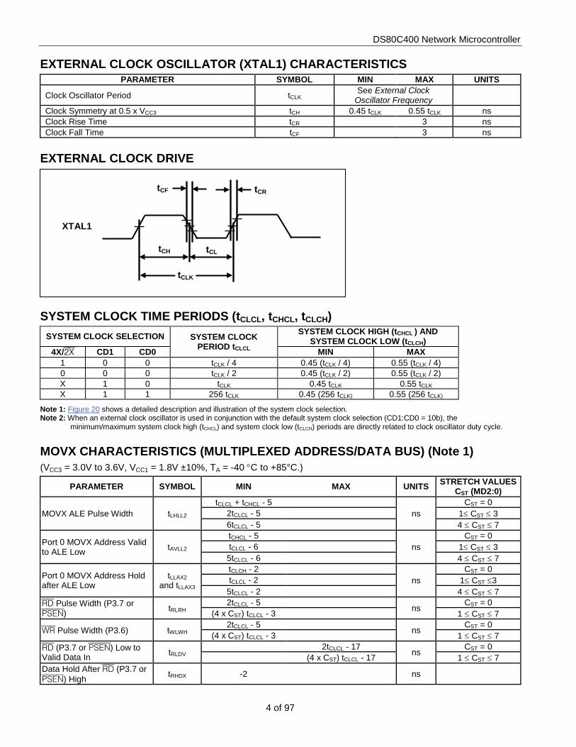
EXTERNAL CLOCK OSCILLATOR (XTAL1) CHARACTERISTICS PARAMETER SYMBOL MIN MAX UNITS
Clock Oscillator Period tCLK See External Clock Oscillator Frequency
Clock Symmetry at 0.5 x VCC3 tCH 0.45 tCLK 0.55 tCLK ns Clock Rise Time tCR 3 ns Clock Fall Time tCF 3 ns
EXTERNAL CLOCK DRIVE SYSTEM CLOCK TIME PERIODS (tCLCL, tCHCL, tCLCH)
SYSTEM CLOCK SELECTION SYSTEM CLOCK PERIOD tCLCL
SYSTEM CLOCK HIGH (tCHCL ) AND SYSTEM CLOCK LOW (tCLCH)
4X/2X CD1 CD0 MIN MAX 1 0 0 tCLK / 4 0.45 (tCLK / 4) 0.55 (tCLK / 4) 0 0 0 tCLK / 2 0.45 (tCLK / 2) 0.55 (tCLK / 2) X 1 0 tCLK 0.45 tCLK 0.55 tCLK X 1 1 256 tCLK 0.45 (256 tCLK) 0.55 (256 tCLK)
Note 1: Figure 20 shows a detailed description and illustration of the system clock selection. Note 2: When an external clock oscillator is used in conjunction with the default system clock selection (CD1:CD0 = 10b), the
minimum/maximum system clock high (tCHCL) and system clock low (tCLCH) periods are directly related to clock oscillator duty cycle. MOVX CHARACTERISTICS (MULTIPLEXED ADDRESS/DATA BUS) (Note 1) (VCC3 = 3.0V to 3.6V, VCC1 = 1.8V ±10%, TA = -40 °C to +85°C.)
PARAMETER SYMBOL MIN MAX UNITS STRETCH VALUES CST (MD2:0)
MOVX ALE Pulse Width tLHLL2 tCLCL + tCHCL - 5
ns CST = 0
2tCLCL - 5 1≤ CST ≤ 3 6tCLCL - 5 4 ≤ CST ≤ 7
Port 0 MOVX Address Valid to ALE Low tAVLL2
tCHCL - 5 ns
CST = 0 tCLCL - 6 1≤ CST ≤ 3
5tCLCL - 6 4 ≤ CST ≤ 7
Port 0 MOVX Address Hold after ALE Low
tLLAX2 and tLLAX3
tCLCH - 2 ns
CST = 0 tCLCL - 2 1≤ CST ≤3
5tCLCL - 2 4 ≤ CST ≤ 7 RD Pulse Width (P3.7 or PSEN) tRLRH
2tCLCL - 5 ns
CST = 0 (4 x CST) tCLCL - 3 1 ≤ CST ≤ 7
WR Pulse Width (P3.6) tWLWH 2tCLCL - 5
ns CST = 0
(4 x CST) tCLCL - 3 1 ≤ CST ≤ 7 RD (P3.7 or PSEN) Low to Valid Data In tRLDV
2tCLCL - 17 ns
CST = 0 (4 x CST) tCLCL - 17 1 ≤ CST ≤ 7
Data Hold After RD (P3.7 or PSEN) High tRHDX -2 ns
tCR tCF
tCLK
tCH
XTAL1
tCL

DS80C400 Network Microcontroller
5 of 97
PARAMETER SYMBOL MIN MAX UNITS STRETCH VALUES CST (MD2:0)
Data Float After RD (P3.7 or PSEN) High tRHDZ
tCLCL - 5 ns
CST = 0 2tCLCL - 5 1≤ CST ≤ 3 6tCLCL - 5 4 ≤ CST ≤ 7
ALE Low to Valid Data In tLLDV 2tCLCL + tCLCH - 19
ns CST = 0
(4 x CST + 1) tCLCL - 19 1≤ CST ≤ 3 (4 x CST + 5) tCLCL - 19 4 ≤ CST ≤ 7
Port 0 Address to Valid Data In tAVDV0
3tCLCL - 19 ns
CST = 0 (4 x CST + 2)tCLCL - 19 1≤ CST ≤ 3 (4 x CST + 10)tCLCL - 19 4 ≤ CST ≤ 7
Port 2, 4, 6 Address, Port 4 CE, or Port 5 PCE to Valid Data In
tAVDV2
3tCLCL + tCLCH - 19
ns
CST = 0
(4 x CST + 2)tCLCL + tCLCH - 19 1≤ CST ≤ 3
(4 x CST + 10)tCLCL + tCLCH - 20 4 ≤ CST ≤ 7
ALE Low to (RD or PSEN) or WR Low tLLWL
tCLCH - 3 tCLCH + 6 ns
CST = 0 tCLCL - 3 tCLCL + 6 1 ≤ CST ≤ 3
5tCLCL - 3 5tCLCL + 6 4 ≤ CST ≤ 7
Port 0 Address to (RD or PSEN) or WR Low tAVWL0
tCLCL - 5 ns
CST = 0 2tCLCL - 6 1 ≤ CST ≤ 3 10tCLCL - 6 4 ≤ CST ≤ 7
Port 2, 4 Address, Port 4 CE, Port 5 PCE, to (RD or PSEN) or WR Low
tAVWL2 tCLCL + tCLCH - 5
ns CST = 0
2tCLCL + tCLCH - 5 1 ≤ CST ≤ 3 10tCLCL + tCLCH - 5 4 ≤ CST ≤ 7
Data Valid to WR Transition tQVWX 0 ns
Data Hold After WR High tWHQX tCLCL - 4
ns CST = 0
2CLCL - 7 1 ≤ CST ≤ 3 6tCLCL - 7 4 ≤ CST ≤ 7
RD Low to Address Float tRLAZ (Note 2) 0≤ CST ≤ 7
(RD or PSEN) or WR High to ALE tWHLH
0 7 ns
CST = 0 tCLCL - 3 tCLCL + 4 1 ≤ CST ≤ 3
5tCLCL - 3 5tCLCL + 4 4 ≤ CST ≤ 7 (RD or PSEN) or WR High to Port 4 CE or Port 5 PCE High
tWHLH2 tCHCL -5 tCHCL + 13
ns CST = 0
tCLCL + tCHCL - 5 tCLCL + tCHCL + 13 1 ≤ CST ≤ 3 5tCLCL + tCHCL - 5 5tCLCL + tCHCL + 13 4 ≤ CST ≤ 7
Note 1: Specifications to -40°C are guaranteed by design and not production tested. Note 2: For a MOVX read operation, on the falling edge of ALE, Port 0 is held by a weak latch until overdriven by external memory. Note 3: All parameters apply to both commercial and industrial temperature operation, unless otherwise noted. Note 4: CST is the stretch cycle value as determined by the MD2, MD1, and MD0 bits of the CKCON register. tCLCL , tCLCH , tCHCL are time
periods associated with the internal system clock and are related to the external clock. See the System Clock Time Periods table. Note 5: All signals characterized with load capacitance of 80pF except Port 0, Port 2, ALE, PSEN, RD, and WR with 100pF. The following
signals, when configured for memory interface, are also characterized with 100pF loading: Port 4 (CE0-3, A16–A19), Port 5.4–5.7 (PCE0-3), Port 6.0–6.5 (CE4-7, A20, A21), Port 7 (demultiplexed mode A0–A7).
Note 6: References to the XTAL, XTAL1, or CLK signal in timing diagrams are to assist in determining the relative occurrence of events, not for determing absolute signal timing with respect to the external clock.
DS80C400 Network Microcontroller
6 of 97

DS80C400 Network Microcontroller
7 of 97

DS80C400 Network Microcontroller
8 of 97
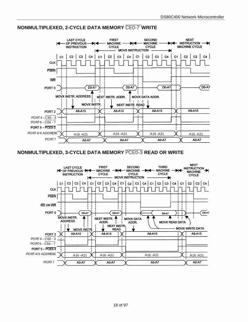
MULTIPLEXED, 2-CYCLE DATA MEMORY PCE0-3 READ
MULTIPLEXED, 2-CYCLE DATA MEMORY CE0-7 READ
PORT 4 – 3CE0 −
PORT 4/6 ADDRESS
PORT 6 – 7−CE4
A16 -A21 A16 -A21 A16 -A21 A16 -A21
PORT 4 – 3CE0 − PORT 6 – 7−CE4
PORT 4/6 ADDRESS A16 -A21 A16 -A21 A16 -A21 A16 -A21

DS80C400 Network Microcontroller
9 of 97
MULTIPLEXED, 2-CYCLE DATA MEMORY CE0-7 WRITE
MULTIPLEXED, 3-CYCLE DATA MEMORY PCE0-3 READ OR WRITE
PORT 4 – 3CE0 − PORT 6 – 7−CE4
PORT 4/6 ADDRESS A16 -A21 A16 -A21 A16 -A21 A16 -A21
PORT 4 – 3CE0 − PORT 6 – 7−CE4
PORT 4/6 ADDRESS A16 -A21 A16 -A21 A16 -A21 A16 -A21

DS80C400 Network Microcontroller
10 of 97
MULTIPLEXED, 3-CYCLE DATA MEMORY CE0-7 READ
MULTIPLEXED, 3-CYCLE DATA MEMORY CE0-7 WRITE
PORT 4 – 3CE0 − PORT 6 – 7−CE4
PORT 4/6 ADDRESS A16 -A21 A16 -A21 A16 -A21 A16 -A21
PORT 4 – 3CE0 − PORT 6 – 7−CE4
PORT 4/6 ADDRESS A16 -A21 A16 -A21 A16 -A21 A16 -A21

DS80C400 Network Microcontroller
11 of 97
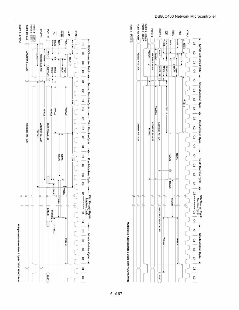
MULTIPLEXED, 9-CYCLE DATA MEMORY PCE0-3 READ OR WRITE
MULTIPLEXED, 9-CYCLE DATA MEMORY CE0-7 READ
PORT 4 – 3CE0 − PORT 6 – 7−CE4
PORT 4/6 ADDRESS A16 -A21 A16 -A21 A16 -A21 A16 -A21
PORT 4 – 3CE0 − PORT 6 – 7−CE4
PORT 4/6 ADDRESS
A16 -A21 A16 -A21 A16 -A21 A16 -A21
DS80C400 Network Microcontroller
12 of 97
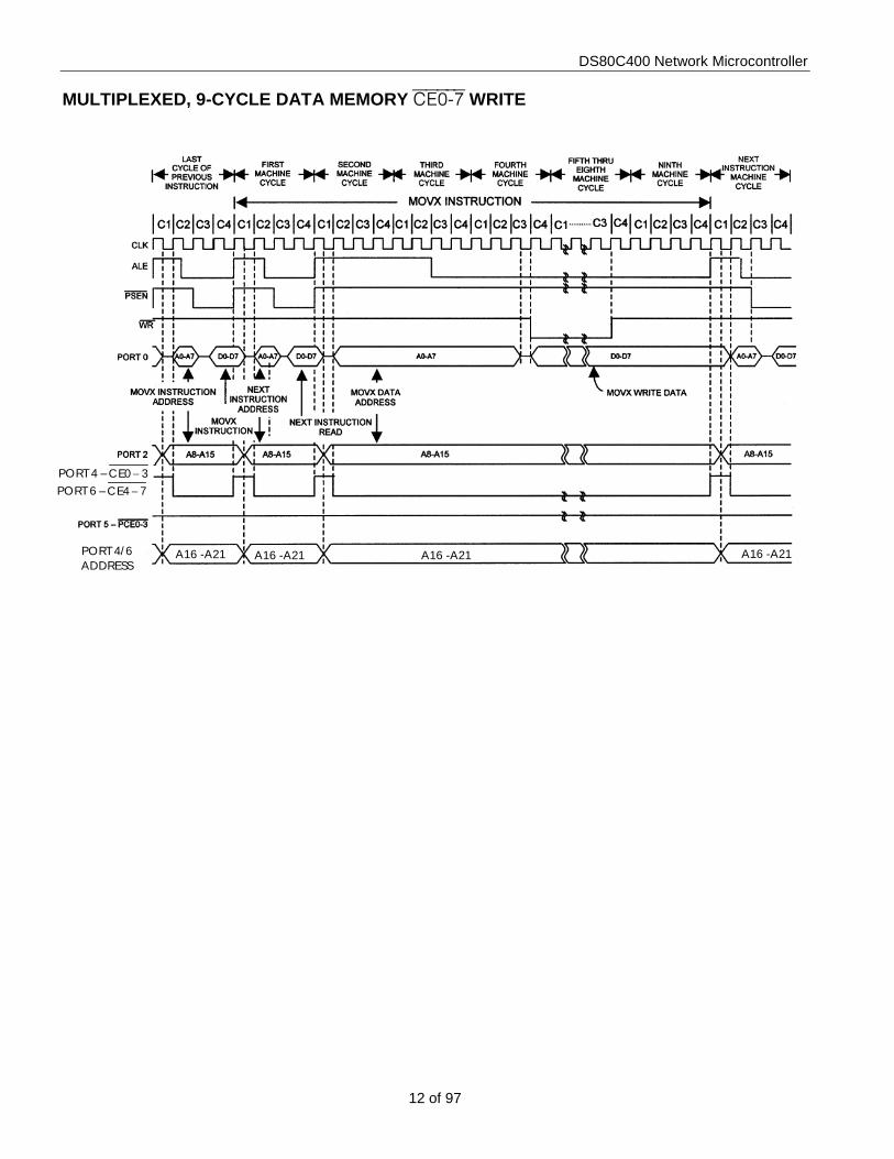
MULTIPLEXED, 9-CYCLE DATA MEMORY CE0-7 WRITE
PORT 4 – 3CE0 − PORT 6 – 7−CE4
PORT 4/6 ADDRESS
A16 -A21 A16 -A21 A16 -A21 A16 -A21

DS80C400 Network Microcontroller
13 of 97
ELECTRICAL CHARACTERISTICS (NONMULTIPLEXED ADDRESS/DATA BUS) (Note 1) (VCC3 = 3.0V to 3.6V, VCC1 = 1.8V ±10%, TA = -40°C to +85°C.)
PARAMETER SYMBOL 75MHz VARIABLE CLOCK UNITS MIN MAX MIN MAX External Crystal Frequency
1 / tCLK 4 40
MHz Clock Mutliplier 2X Mode 16 37.5 Clock Multiplier 4X Mode 11 18.75 External Oscillator Frequency
1 / tCLK DC 75
MHz Clock Mutliplier 2X Mode 16 37.5 Clock Multiplier 4X Mode 11 18.75 PSEN Pulse Width tPLPH 21.7 2tCLCL - 5 ns PSEN Low to Valid Instruction In tPLIV 9.7 2tCLCL - 17 ns Input Instruction Hold After PSEN tPXIX 0 0 ns
Input Instruction Float After PSEN tPXIZ See MOVX Characteristics ns
Port 7 Address to Valid Instruction In tAVIV1 21.0 3tCLCL - 19 ns Port 2, 4, 6 Address or Port 4 CE to Valid Instruction In tAVIV2 27.7 3tCLCL + tCLCH - 19 ns
Note 1: Specifications to -40°C are guaranteed by design and not production tested. Note 2: All parameters apply to both commercial and industrial temperature operation, unless otherwise noted. Note 3: tCLCL, tCLCH, tCHCL are time periods associated with the internal system clock and are related to the external clock (tCLK) as defined in the
the System Clock Time Periods table. Note 4: The precalculated 75MHz min/max timing specifications assume an exact 50% duty cycle. Note 5: All signals characterized with load capacitance of 80pF except Port 0, Port 2, ALE, PSEN, RD, and WR with 100pF. The following
signals, when configured for memory interface, are also characterized with 100pF loading: Port 4 (CE0-3, A16–A19), Port 5.4–5.7 (PCE0-3), Port 6.0–6.5 (CE4-7, A20, A21), Port 7 (demultiplexed mode A0–A7).
Note 6: References to the XTAL, XTAL1, or CLK signal in timing diagrams is to assist in determining the relative occurrence of events, not for determing absolute signal timing with respect to the external clock.

DS80C400 Network Microcontroller
14 of 97
MOVX CHARACTERISTICS (NONMULTIPLEXED ADDRESS/DATA BUS) (Note 1) (VCC3 = 3.0V to 3.6V, VCC1 = 1.8V +±10%, TA = -40°C to +85°C.)
PARAMETER SYMBOL MIN MAX UNITS STRETCH VALUES
CST (MD2:0)
Input Instruction Float After PSEN tPXIZ 2tCLCL - 5
ns CST = 0
3tCLCL - 5 1≤ CST ≤ 3 11tCLCL - 5 4 ≤ CST ≤ 7
PSEN High to Data Address, Port 4 CE, Port 5 PCE Valid tPHAV tCHCL - 3 ns
RD Pulse Width (P3.7 or PSEN) tRLRH 2tCLCL - 5 ns CST =0 (4 x CST) tCLCL - 3 1 ≤ CST ≤ 7
WR Pulse Width (P3.6) tWLWH 2tCLCL - 5 ns CST =0 (4 x CST)tCLCL - 3 1 ≤ CST ≤ 7
RD (P3.7 or PSEN) Low to Valid Data In tRLDV 2tCLCL - 17 ns CST = 0 (4 x CST)tCLCL - 17 1 ≤ CST ≤ 7
Data Hold After RD (P3.7 or PSEN) High tRHDX -2 ns
Data Float After RD (P3.7 or PSEN) High tRHDZ tCLCL - 5
ns CST = 0
2tCLCL - 5 1≤ CST ≤ 3 6tCLCL - 5 4 ≤ CST ≤ 7
PSEN High to WR Low tPHWL 2tCLCL - 3
ns CST = 0
3tCLCL - 3 1≤ CST ≤ 3 11tCLCL - 3 4 ≤ CST ≤ 7
PSEN High to (RD or PSEN) Low tPHRL 2tCLCL - 3
ns CST = 0
3tCLCL - 3 1≤ CST ≤ 3 11tCLCL - 3 4 ≤ CST ≤ 7
Port 7 Address to Valid Data In tAVDV1
3tCLCL - 19
ns
CST = 0 (4 x CST + 2)tCLCL- 19 1≤ CST ≤ 3
(4 x CST + 10)tCLCL - 19 4 ≤ CST ≤ 7
Port 2, 4, 6 Address, Port 4 CE or Port 5 PCE to Valid Data In tAVDV2
3tCLCL + tCLCH - 19
ns
CST = 0
(4 x CST + 2)tCLCL + tCLCH - 19 1≤ CST ≤ 3
(4 x CST + 10)tCLCL + tCLCH - 19 4 ≤ CST ≤ 7
Port 7 Address to (RD or PSEN) or WR Low tAVWL1
tCLCL - 5 ns
CST = 0 2tCLCL - 5 1 ≤ CST ≤ 3 10tCLCL - 5 4 ≤ CST ≤ 7
Port 2, 4, 6 Address, Port 4 CE or Port 5 PCE to (RD or PSEN) or WR Low tAVWL2
tCLCL + tCLCH - 5 ns
CST = 0 2tCLCL + tCLCH - 5 1 ≤ CST ≤ 3
10tCLCL + tCLCH - 5 4 ≤ CST ≤ 7 Data Valid to WR Transition tQVWX 0 ns
Data Hold After WR High tWHQX tCLCL - 4
ns CST = 0
2CLCL - 7 1 ≤ CST ≤ 3 6tCLCL - 7 4 ≤ CST ≤ 7
(RD or PSEN) or WR High to Port 4 CE or Port 5 PCE High tWHCEH
tCHCL - 5 tCHCL + 13 ns
CST = 0 tCLCL + tCHCL - 5 tCLCL + tCHCL +12 1 ≤ CST ≤ 3 5tCLCL + tCHCL -5 5tCLCL + tCHCL +12 4 ≤ CST ≤ 7
Note 1: Specifications to -40°C are guaranteed by design and not production tested. Note 2: All parameters apply to both commercial and industrial temperature operation unless otherwise noted. Note 3: CST is the stretch cycle value as determined by the MD2, MD1, and MD0 bits of the CKCON register. tCLCL, tCLCH, tCHCL are time periods
associated with the internal system clock and are related to the external clock. See the System Clock Time Periods table. Note 4: All signals characterized with load capacitance of 80pF except Port 0, Port 2, ALE, PSEN, RD, and WR with 100pF. The following
signals, when configured for memory interface, are also characterized with 100pF loading: Port 4 (CE0-3, A16–A19), Port 5.4–5.7 (PCE0-3), Port 6.0–6.5 (CE4-7, A20, A2), Port 7 (demultiplexed mode A0–A7).
Note 5: References to the XTAL or CLK signal in timing diagrams is to assist in determining the relative occurrence of events, not for determing absolute signal timing with respect to the external clock.

DS80C400 Network Microcontroller
15 of 97
DS80C400 Network Microcontroller
16 of 97
l

DS80C400 Network Microcontroller
17 of 97
NONMULTIPLEXED, 2-CYCLE DATA MEMORY PCE0-3 READ OR WRITE
NONMULTIPLEXED, 2-CYCLE DATA MEMORY CE0-7 READ
PORT 4 – 3CE0 − PORT 6 – 7−CE4
PORT 4/6 ADDRESS A16 -A21 A16 -A21 A16 -A21 A16 -A21
PORT 4 – 3CE0 − PORT 6 – 7−CE4
PORT 4/6 ADDRESS A16 -A21 A16 -A21 A16 -A21 A16 -A21 PORT 7
DS80C400 Network Microcontroller
18 of 97
NONMULTIPLEXED, 2-CYCLE DATA MEMORY CE0-7 WRITE
NONMULTIPLEXED, 3-CYCLE DATA MEMORY PCE0-3 READ OR WRITE
PORT 4 – 3CE0 − PORT 6 – 7−CE4
PORT 4/6 ADDRESS A16 -A21 A16 -A21 A16 -A21 A16 -A21 PORT 7
PORT 4 – 3CE0 − PORT 6 – 7−CE4
PORT 4/6 ADDRESS A16 -A21 A16 -A21 A16 -A21 A16 -A21 PORT 7
DS80C400 Network Microcontroller
19 of 97
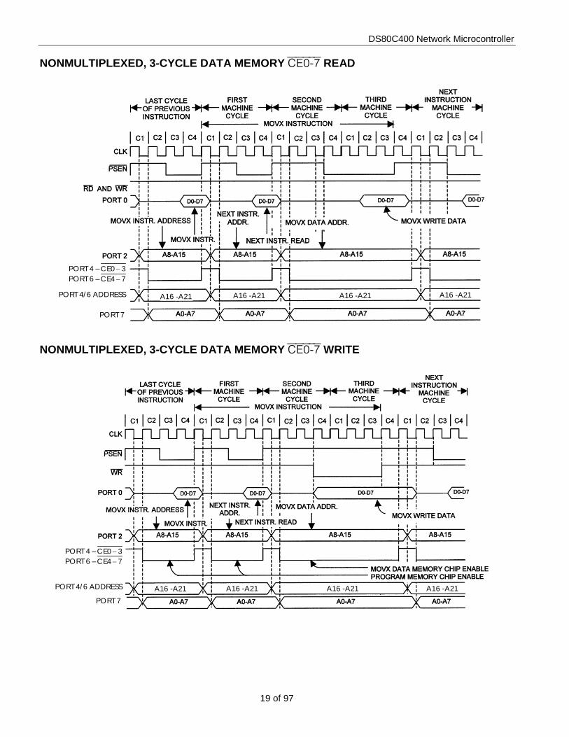
NONMULTIPLEXED, 3-CYCLE DATA MEMORY CE0-7 READ
NONMULTIPLEXED, 3-CYCLE DATA MEMORY CE0-7 WRITE
PORT 4 – 3CE0 − PORT 6 – 7−CE4
PORT 4/6 ADDRESS A16 -A21 A16 -A21 A16 -A21 A16 -A21 PORT 7
PORT 4 – 3CE0 − PORT 6 – 7−CE4 PORT 4/6 ADDRESS A16 -A21 A16 -A21 A16 -A21 A16 -A21
PORT 7
DS80C400 Network Microcontroller
20 of 97
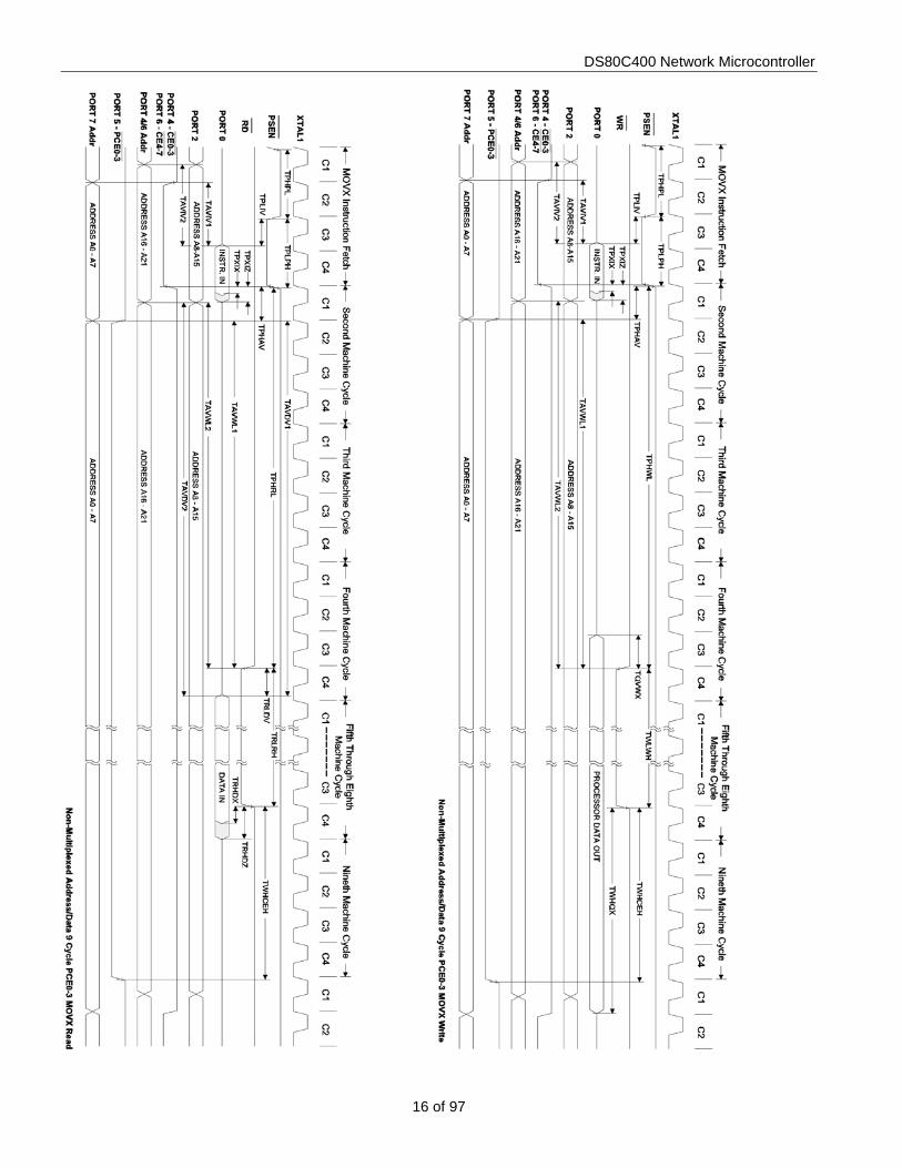
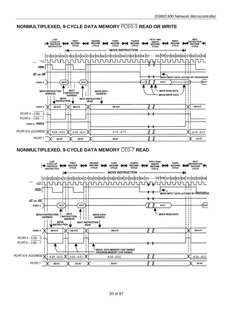
NONMULTIPLEXED, 9-CYCLE DATA MEMORY PCE0-3 READ OR WRITE
NONMULTIPLEXED, 9-CYCLE DATA MEMORY CE0-7 READ
PORT 4 – 3CE0 − PORT 6 – 7−CE4
PORT 4/6 ADDRESS A16 -A21 A16 -A21 A16 -A21 A16 -A21 PORT 7
PORT 4 – 3CE0 − PORT 6 – 7−CE4
PORT 4/6 ADDRESS A16 -A21 A16 -A21 A16 -A21 A16 -A21 PORT 7

DS80C400 Network Microcontroller
21 of 97
NONMULTIPLEXED, 9-CYCLE DATA MEMORY CE0-7 WRITE
OW PIN TIMING CHARACTERISTICS (Note 1) (VCC3 = 3.0V to 3.6V, VCC1 = 1.8V ±10%, TA = -40°C to +85°C.)
PARAMETER SYMBOL STANDARD OVERDRIVE LONGLINE UNITS MIN MAX MIN MAX MIN MAX Transmit Reset Pulse Low Time (Note 2) tRSTL 500.8 626 50.4 63 500.8 626 µs Transmit Reset Pulse High Time (Note 2) tRSTH 508.8 636 59.2 74 508.8 636 µs Wait Time for Transmit of Presence Pulse (Notes 2, 3) tPDH 15 60 2 6 15 60 µs Wait Time for Absence of Presence Pulse (Notes 2, 4) tPDHCNT 60 75 6.4 8 60 75 µs
Presence Pulse Width (Note 2) tPDL 60 240 8 24 60 240 µs Presence Pulse Sampling Time (Note 2) tPDS 24 31 2.4 4 30.4 38 µs
Read/Write Data Time Slot tSLOT 68.8 86 12 15 68.8 86 µs Low Time for Write 1 tLOW1 4.8 6 0.8 1 7.2 9 µs Low Time for Write 0 tLOW0 62.4 78 8 10 62.4 78 µs Write Data Sampling Time tWDV 15 60 2 6 25 60 µs Read Data Sampling Time tRDV 12 15 1.6 2 20 25 µs
Note 1: Specifications to -40°C are guaranteed by design and not production tested. Note 2: In PMM mode, the master pulls the line low after the first 15µs for the remainder of the standard speed 1-Wire routine. Note 3: This parameter quantifies the wait time for the slave devices to respond to the reset pulse and is dependent on the slave device timing. Note 4: This parameter quantifies the wait time for the case when no presence pulse detected. Note 5: The maximum timing figures shown apply only when an exact 1-Wire clock frequency can be achieved from the microcontroller input
clock.
PORT 4 – 3CE0 − PORT 6 – 7−CE4
PORT 4/6 ADDRESS A16 -A21 A16 -A21 A16 -A21 A16 -A21 PORT 7

DS80C400 Network Microcontroller
22 of 97
OW PIN TIMING

DS80C400 Network Microcontroller
23 of 97
OWSTP PIN TIMING CHARACTERISTICS (Note 1) (VCC3 = 3.0V to 3.6V, VCC1 = 1.8V ±10%, TA = -40°C to +85°C.)
PARAMETER SYMBOL STANDARD OVERDRIVE UNITS MIN MAX MIN MAX Active Time for Presence Detect tON1 6.4 8 0.8 1 µs Active Time for Presence Detect Recovery tON2 8 10 8 10 µs Active Time for Write 1 Recovery (Notes 2, 3) tON3 51.2 64 7.2 9 µs Active Time for Write 0 Recovery (Notes 2, 3) tON4 6.4 8 0.8 1 µs Delay Time for Presence Detect tDLY1 0.8 1 0.8 1 µs Delay Time for Presence Detect Recovery (Note 4) tDLY2 399.2 499 31.2 39 µs Delay Time for Write 1/Write 0 Recovery tDLY3 0.8 1 0.8 1 µs Turn-Off Time for 1-Wire Reset tOFF1 1.6 2 1.6 2 µs Turn-Off Time for Write 1/Write 0 (Note 5) tOFF2 0.8 1 0.8 1 µs
Note 1: Specifications to -40°C are guaranteed by design and not production tested. Note 2: There is no OWSTP timing difference for sending out and receiving bits within a byte. The difference comes when the last bit of the byte
has been completely sent. At this point, the signal is either enabled continuously until the next reset or time slot begins, or enabled only for active time write 1 or write 0.
Note 3: When performing a read versus a write time slot, the master provides the same active time for write 1 and write 0. However, the Schmitt-triggered input from the OW line is sensed every 1µs for a high value. If OW is high, the OWSTP signal is enabled. If the OW line is low, the OWSTP signal remains disabled until a high state is sensed. In all write time slots, a high is sensed immediately.
Note 4: This parameter is the time delay until the master begins to monitor the OW pin level. If the line is already high, then OWSTP is enabled. If not, it waits to enable OWSTP until the next state machine clock (1µs or 50ns) after the OW line recovers.
Note 5: The very first bit in a byte has an extended turn-off time of 4µs because of the order of states that the 1-Wire master state machine must go through.
OWSTP PIN TIMING
DS80C400 Network Microcontroller
24 of 97
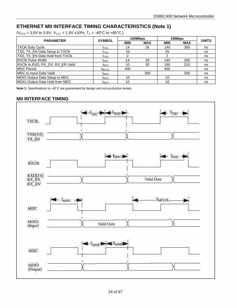
ETHERNET MII INTERFACE TIMING CHARACTERISTICS (Note 1) (VCC3 = 3.0V to 3.6V, VCC1 = 1.8V ±10%, TA = -40°C to +85°C.)
PARAMETER SYMBOL 100Mbps 10Mbps UNITS MIN MAX MIN MAX TXClk Duty Cycle tTDC 14 26 140 260 ns TXD, TX_EN Data Setup to TXClk tTSU 10 25 ns TXD, TX_EN Data Hold from TXClk tTHD 2 2 ns RXClk Pulse Width tRDC 14 26 140 260 ns RXClk to RXD, RX_DV, RX_ER Valid tRDV 10 30 190 210 ns MDC Period tMCLCL 400 400 ns MDC to Input Data Valid tMDV 300 300 ns MDIO Output Data Setup to MDC tMOS 10 10 ns MDIO Output Data Hold from MDC tMOH 10 10 ns
Note 1: Specifications to -40°C are guaranteed by design and not production tested.
MII INTERFACE TIMING

DS80C400 Network Microcontroller
25 of 97
SERIAL PORT MODE 0 TIMING CHARACTERISTICS (Note 1) (VCC3 = 3.0V to 3.6V, VCC1 = 1.8V ±10%, TA = -40°C to +85°C.)
PARAMETER SYMBOL CONDITIONS MIN TYP MAX UNITS
Serial Port Clock Cycle Time tXLXL SM2 = 0:12 clocks per cycle 12 tCLCL
ns SM2 = 1:4 clocks per cycle 4 tCLCL
Output Data Setup to Clock Rising tQVXH
SM2 = 0:12 clocks per cycle 10 tCLCL - 10
ns SM2 = 1:4 clocks per cycle 3 tCLCL -
10
Output Data Hold from Clock Rising tXHQX
SM2 = 0:12 clocks per cycle 2 tCLCL - 10 ns
SM2 = 1:4 clocks per cycle tCLCL - 10
Input Data Hold After Clock Rising tXHDX
SM2 = 0:12 clocks per cycle 0 ns
SM2 = 1:4 clocks per cycle 0
Clock Rising Edge to Input Data Valid tXHDV
SM2 = 0:12 clocks per cycle 11 tCLCL - 20 ns
SM2 = 1:4 clocks per cycle 3 tCLCL - 20
Note 1: Specifications to -40°C are guaranteed by design and not production tested.

DS80C400 Network Microcontroller
26 of 97
SERIAL PORT 0 (SYNCHRONOUS MODE)
TRADITIONAL 8051 OPERATION, TXD CLOCK = XTAL/12 (SM2 = 0)
HIGH-SPEED OPERATION, TXD CLK = SYSCLK/4 (SM2 = 1)

DS80C400 Network Microcontroller
27 of 97
POWER-CYCLE TIMING CHARACTERISTICS
PARAMETER SYMBOL MIN TYP MAX UNITS
Crystal Startup Time (Note 1) tCSU 1.8 ms Power-On Reset Delay (Note 2) tPOR 65,536 tCLCK
Note 1: Startup time for crystals varies with load capacitance and manufacturer. Time shown is for an 11.0592MHz crystal manufactured by Fox Electronics.
Note 2: Reset delay is a synchronous counter of crystal oscillations during crystal startup. Counting begins when the level on the XTAL1 input meets the VIH2 criteria. At 40MHz, this time is approximately 1.64ms.
POWER-CYCLE TIMING

DS80C400 Network Microcontroller
28 of 97
BLOCK DIAGRAM
OW
O
WST
P
V CC
1 (1)
V C
C3 (
4)
V SS (4
) R
ST
RST
OL
MU
X
EA
PSEN
AL
E
XTAL
1 XT
AL2
AD
DR
ES
S B
US
DA
TA B
US
PORT 1
POR
T 7
POR
T LA
TCH
POR
T 6
POR
T LA
TCH
POR
T LA
TCH
POR
T 3
PORT LATCH
PORT 5
MII
MAN
AGE
MEN
T M
II
I/O
SERIALPORT 1
SER
IAL
POR
T 0
SER
IAL
POR
T 2
TIMER 2
TIM
ER 0
TIM
ER 1
TIM
ER 3
CAN
0
CO
NTR
OLL
ER
CAN
SR
AM
25
6 x
8
BUFF
ER C
ON
TRO
L U
NIT
AC
CU
MU
LATO
R
POR
T LA
TCH
POR
T 4
OS
CIL
LATO
R
POR
T 2
POR
T LA
TCH
PORT 0 1-WIRE CONTROLLER
PORT LATCH SR
AM
9k
k x
8
V CC P
OW
ER
MO
NIT
OR
RES
ET
CO
NTR
OL
OS
CIL
LATO
R-
FAIL
DE
TEC
T
PS
W
STA
CK
P
OIN
TER
S
FRs/
SR
AM
256
x 8
INTE
RR
UP
T LO
GIC
MA
TH
AC
CE
LER
ATO
R
TIM
ED
A
CC
ESS
DP
TR0
DP
TR1
DP
TR2
DP
TR3
PR
OG
RA
M
CO
UN
TER
ON
E’S
CO
MP
. A
DD
ER
INTR
UC
TIO
N
RE
GIS
TER
B
OO
T R
OM
64
k x
8 W
ATC
HD
OG
P6.0
–P6.
7 P4
.0–
4.7
P2.0
–P2.
7 P7
.0–P
7.7
P3.0
–P3.
7
P5.0–P5.7
P1.0–P1.7 P0.0–P0.7
CLO
CK
AND
M
EMO
RY
C
ON
TRO
L
MD
C
MD
IO
MII
I/O (1
5)
B
DS80C400

DS80C400 Network Microcontroller
29 of 97
PIN DESCRIPTION PIN NAME FUNCTION
70 VCC1 +1.8V Core Supply Voltage 12, 36, 62,
87 VCC3 +3.3V I/O Supply Voltage
13, 39, 63, 88 VSS Digital Circuit Ground
68 ALE
Address Latch Enable, Output. When the MUX pin is low, this pin outputs a clock to latch the external address LSB from the multiplexed address/data bus on Port 0. This signal is commonly connected to the latch enable of an external transparent latch. ALE has a pulse width of 1.5 XTAL1 cycles and a period of four XTAL1 cycles. When the MUX pin is high, the pin toggles continuously if the ALEOFF bit is cleared. ALE is forced high when the device is in a reset condition or if the ALEOFF bit is set while the MUX pin is high.
67 PSEN Program Store Enable, Output. This signal is the chip enable for external program or merged program/data memory. PSEN provides an active-low pulse and is driven high when external memory is not being accessed.
69 EA External Access Enable, Input. Connect to GND to use external program memory. Connect to VCC to use internal ROM.
40 MUX Multiplex/Demultiplex Select, Input. This pin selects if the address/data bus operates in multiplexed (MUX = 0) or demultiplexed (MUX = 1) mode. The MUX pin is sampled only on a power-on reset.
97 RST Reset, Input. The RST input pin contains a Schmitt voltage input to recognize external active-high reset inputs. The pin also employs an internal pulldown resistor to allow for a combination of wired-OR external-reset sources. An RC circuit is not required for power-up, as the device provides this function internally.
98 RSTOL
Reset Output Low, Output. This active-low signal is asserted when the microcontroller has entered reset through the RST pin; during crystal warm-up period following power-on or stop mode; during a watchdog timer reset; during an oscillator failure (if OFDE = 1); whenever VCC1 ≤ VRST1 or VCC3 ≤ VRST3. When connecting the DS80C400 to an external PHY, do not connect the RSTOL to the reset of the PHY. Doing so may disable the Ethernet transmit.
37 XTAL2 XTAL1, XTAL2. Crystal oscillator pins support fundamental mode, parallel resonant, AT cut crystals. XTAL1 is the input if an external clock source is used in place of a crystal. XTAL2 is the output of the crystal amplifier. 38 XTAL1
86 AD0/D0 AD0–7 (Port 0), I/O. When the MUX pin is connected low, Port 0 is the multiplexed address/data bus. While ALE is high, the LSB of a memory address is presented. While ALE falls, the port transitions to a bidirectional data bus. When the MUX pin is connected high, Port 0 functions as the bidirectional data bus. Port 0 cannot be modified by software. The reset condition of Port 0 pins is high. No pullup resistors are needed.
Port Alternate Function P0.0 AD0/D0 (Address)/Data 0 P0.1 AD1/D1 (Address)/Data 1 P0.2 AD2/D2 (Address)/Data 2 P0.3 AD3/D3 (Address)/Data 3 P0.4 AD4/D4 (Address)/Data 4 P0.5 AD5/D5 (Address)/Data 5 P0.6 AD6/D6 (Address)/Data 6 P0.7 AD7/D7 (Address)/Data 7
85 AD1/D1
84 AD2/D2
83 AD3/D3
82 AD4/D4
81 AD5/D5
80 AD6/D6
79 AD7/D7
89 P1.0 Port 1, I/O. Port 1 can function as either an 8-bit, bidirectional I/O port or as an alternate interface for internal resources. The reset condition of Port 1 is all bits at logic 1 through a weak pullup. The logic 1 state also serves as an input mode, since external circuits writing to the port can override the weak pullup. When software clears any port pin to 0, a strong pulldown is activated that remains on until either a 1 is written to the port pin or a reset occurs. Writing a 1 after the port has been at 0 activates a strong transition driver, followed by a weaker sustaining pullup. Once the momentary strong driver turns off, the port once again becomes the output (and input) high state. Port Alternate Function P1.0 T2 External I/O for Timer/Counter 2 P1.1 T2EX Timer/Counter 2 Capture/Reload Trigger P1.2 RXD1 Serial Port 1 Receive P1.3 TXD1 Serial Port 1 Transmit P1.4 INT2 External Interrupt 2 (Positive Edge Detect) P1.5 INT3 External Interrupt 3 (Negative Edge Detect) P1.6 INT4 External Interrupt 4 (Positive Edge Detect) P1.7 INT5 External Interrupt 5 (Negative Edge Detect)
90 P1.1
91 P1.2
92 P1.3
93 P1.4
94 P1.5
95 P1.6
96 P1.7
66 A8 A15–A8 (Port 2), Output. Port 2 serves as the MSB for external addressing. The port automatically asserts the address MSB during external ROM and RAM access. Although the Port 2 SFR exists, the SFR value never appears on the pins (due to memory access). Therefore, accessing the Port 2 SFR is only useful for MOVX A, @Ri or MOVX @Ri, A instructions, which use the Port 2 SFR as the external address MSB. Port Alternate Function P2.0 A8 Program/Data Memory Address 8 P2.1 A9 Program/Data Memory Address 9
65 A9
64 A10
61 A11
60 A12

DS80C400 Network Microcontroller
30 of 97
PIN NAME FUNCTION
59 A13 P2.2 A10 Program/Data Memory Address 10 P2.3 A11 Program/Data Memory Address 11 P2.4 A12 Program/Data Memory Address 12 P2.5 A13 Program/Data Memory Address 13 P2.6 A14 Program/Data Memory Address 14 P2.7 A15 Program/Data Memory Address 15
58 A14
57 A15
20 P3.0 Port 3, I/O. Port 3 functions as an 8-bit, bidirectional I/O port, and as an alternate interface for several resources found on the traditional 8051. The reset condition of Port 3 is all bits at logic 1 through a weak pullup. The logic 1 state also serves as an input mode, since external circuits writing to the port can override the weak pullup. When software clears any port pin to 0, the device activates a strong pulldown that remains on until either a 1 is written to the port pin or a reset occurs. Writing a 1 after the port has been at 0 activates a strong transition driver, followed by a weaker sustaining pullup. Once the momentary strong driver turns off, the port once again becomes the output (and input) high state. Port Alternate Function P3.0 RXD0 Serial Port 0 Receive P3.1 TXD0 Serial Port 0 Transmit P3.2 INT0 External Interrupt 0 P3.3 INT1 External Interrupt 1 P3.4 T0 Timer 0 External Input P3.5 T1/CLKO Timer 1 External Input/External Clock Output P3.6 WR External Data Memory Write Strobe P3.7 RD External Data Memory Read Strobe
21 P3.1
22 P3.2
23 P3.3
24 P3.4
25 P3.5
26 P3.6
27 P3.7
48 P4.0 Port 4, I/O. Port 4 is composed of eight pins that are user programmable as I/O, extended program memory chip enables, or extended address lines. The configuration of the eight pins is established through the programming of the port 4 control register (P4CNT). Following a reset, and if EA is low, P4.3 to P4.1 are driven high and are assigned as chip enables. Port pins P4.7 to P4.4 and P4.0 are cleared to low state and are assigned as addresses and chip enable, respectively. Additional information on external memory interfacing is found in the port 4 control register SFR description and other sections in the High-Speed Microcontroller User’s Guide: Network Microcontroller Supplement. Port Alternate Function P4.0 CE0 Program Memory Chip Enable 0 P4.1 CE1 Program Memory Chip Enable 1 P4.2 CE2 Program Memory Chip Enable 2 P4.3 CE3 Program Memory Chip Enable 3 P4.4 A16 Program/Data Memory Address 16 P4.5 A17 Program/Data Memory Address 17 P4.6 A18 Program/Data Memory Address 18 P4.7 A19 Program/Data Memory Address 19
47 P4.1
46 P4.2
45 P4.3
44 P4.4
43 P4.5
42 P4.6
41 P4.7
35 P5.0 Port 5, I/O. Port 5 can function as an 8-bit, bidirectional I/O port, the CAN interface, Timer 3 input, and/or as peripheral-enable signals. The reset condition of Port 5 is all bits at logic 1 through a weak pullup. The logic 1 state also serves as an input mode, since external circuits writing to the port can override the weak pullup. When software clears any port pin to 0, the device activates a strong pulldown that remains on until either a 1 is written to the port pin or a reset occurs. Writing a 1 after the port has been at 0 activates a strong transition driver, followed by a weaker sustaining pullup. Once the momentary strong driver turns off, the port once again becomes the output (and input) high state. Port Alternate Function P5.0 C0TX CAN0 Transmit Output P5.1 C0RX CAN0 Receive Input P5.2 T3 Timer 3 External Input P5.3 None P5.4 PCE0 Peripheral Chip Enable 0 P5.5 PCE1 Peripheral Chip Enable 1 P5.6 PCE2 Peripheral Chip Enable 2 P5.7 PCE3 Peripheral Chip Enable 3
34 P5.1
33 P5.2
32 P5.3
31 P5.4
30 P5.5
29 P5.6
28 P5.7
56 P6.0 Port 6, I/O. Port 6 can function as an 8-bit, bidirectional I/O port, as program and data memory address/chip-enable signals, and/or a third serial port. The reset condition of Port 6 is all bits at logic 1 through a weak pullup. The logic 1 state also serves as an input mode, since external circuits writing to the port can override the weak pullup. When software clears any port pin to 0, the device activates a strong pulldown that remains on until either a 1 is written to the port pin or a reset occurs. Writing a 1 after the port has been at 0 activates a strong transition driver, followed by a weaker sustaining pullup. Once the momentary strong driver turns off, the port once again becomes the output (and input) high state. Port Alternate Function P6.0 CE4 Program Memory Chip Enable 4
55 P6.1
54 P6.2
53 P6.3
52 P6.4

DS80C400 Network Microcontroller
31 of 97
PIN NAME FUNCTION
51 P6.5 P6.1 CE5 Program Memory Chip Enable 5 P6.2 CE6 Program Memory Chip Enable 6 P6.3 CE7 Program Memory Chip Enable 7 P6.4 A20 Program/Data Memory Address 20 P6.5 A21 Program/Data Memory Address 21 P6.6 RXD2 Serial Port 2 Receive P6.7 TXD2 Serial Port 2 Transmit
50 P6.6
49 P6.7
78 A0 Port 7, I/O. Port 7 can function as either an 8-bit, bidirectional I/O port or the nonmultiplexed A0–A7 signals (when the MUX pin = 1). The reset condition of Port 7 is all bits at logic 1 through a weak pullup. The logic 1 state also serves as an input mode, since external circuits writing to the port can override the weak pullup. When software clears any port pin to 0, a strong pulldown is activated that remains on until either a 1 is written to the port pin or a reset occurs. Writing a 1 after the port has been at 0 activates a strong transition driver, followed by a weaker sustaining pullup. Once the momentary strong driver turns off, the port once again becomes the output (and input) high state. Port Alternate Function P7.0 A0 Program/Data Memory Address 0 P7.1 A1 Program/Data Memory Address 1 P7.2 A2 Program/Data Memory Address 2 P7.3 A3 Program/Data Memory Address 3 P7.4 A4 Program/Data Memory Address 4 P7.5 A5 Program/Data Memory Address 5 P7.6 A6 Program/Data Memory Address 6 P7.7 A7 Program/Data Memory Address 7
77 A1
76 A2
75 A3
74 A4
73 A5
72 A6
71 A7
8 TXClk
Transmit Clock, Input. The transmit clock is a continuous clock sourced from the Ethernet PHY controller. It is used to provide timing reference for transferring of TX_EN and TXD[3:0] signals from the MAC to the external Ethernet PHY controller. The input clock frequency of TXClk should be 25MHz for 100Mbps operation and 2.5MHz for 10Mbps operation. For ENDEC operation, TXClk serves the same function, but the input clock frequency should be 10MHz.
7 TX_EN
Transmit Enable, Output. The transmit enable is an active-high output and is synchronous with respect to the TXClk signal. TX_EN is used to indicate valid nibbles of data for transmission on the MII pins TXD.3–TXD.0. TX_EN is asserted with the first nibble of the preamble and remains asserted while all nibbles to be transmitted are presented on the TXD.3–TXD.0 pins. TX_EN negates prior to the first TXClk following the final nibble of the frame. TX_EN serves the same function for ENDEC operation.
3 TXD.3 Transmit Data, Output. The transmit data outputs provide 4-bit nibbles of data for transmission over the MII. The transmit data is synchronous with respect to the TXClk signal. For each TXClk period when TX_EN is asserted, TXD.3–TXD.0 provides the data for transmission to the Ethernet PHY controller. When TX_EN is deasserted, the TXD data should be ignored. For ENDEC operation, only TXD.0 is used for transmission of frames.
4 TXD.2 5 TXD.1 6 TXD.0
10 RXClk
Receive Clock, Input. The receive clock is a continuous clock sourced from the Ethernet PHY controller. It is used to provide timing reference for transferring of RX_DV, RX_ER, and RXD[3:0] signals from the external Ethernet PHY controller to the MAC. The input clock frequency of RXClk should be 25MHz for 100Mbps operation and 2.5MHz for 10Mbps operation. For ENDEC operation, RXClk serves the same function, but the input clock frequency should be 10MHz.
11 RX_DV
Receive Data Valid, Input. The receive data valid is an active-high input from the external Ethernet PHY controller and is synchronous with respect to the RXClk signal. RX_DV is used to indicate valid nibbles of data for reception on the MII pins RXD.3–RXD.0. RX_DV is asserted continuously from the first nibble of the frame through the final nibble. RX_DV negates prior to the first RXClk following the final nibble. RX_DV serves the same function for ENDEC operation.
9 RX_ER
Receive Error, Input. The receive error is an active-high input from the external Ethernet PHY controller and is synchronous with respect to the RXClk signal. RX_ER is used to indicate to the MAC that an error (e.g., a coding error, or any error detectable by the PHY) was detected somewhere in the frame presently being transmitted by the PHY. RX_ER has no effect on the MAC while RX_DV is deasserted. RX_ER should be low for ENDEC operation.
17 RXD.3 Receive Data, Input. The receive data inputs provide 4-bit nibbles of data for reception over the MII. The receive data is synchronous with respect to the RXClk signal. For each RXClk period when RX_DV is asserted, RXD.3–RXD.0 have the data to be received by the MAC. When RX_DV is deasserted, the RXD data should be ignored. For ENDEC operation, only RXD.0 is used for reception of frames.
16 RXD.2 15 RXD.1 14 RXD.0
1 CRS
Carrier Sense, Input. The carrier sense signal is an active-high input and should be asserted by the external Ethernet PHY controller when either the transmit or receive medium is not idle. CRS should be deasserted by the PHY when the transmit and receive mediums are idle. The PHY should ensure that the CRS signal remains asserted throughout the duration of a collision condition. The transitions on the CRS signal need not be synchronous to TXClk or RXClk. CRS serves the same function for ENDEC operation.
2 COL
Collision Detect, Input. The collision detect signal is an active-high input and should be asserted by the external Ethernet PHY controller upon detection of a collision on the medium. The PHY should ensure that COL remains asserted while the collision condition persists. The transitions on the COL signal need not be synchronous to TXClk or RXClk. The COL signal is ignored by the MAC when operating in full-duplex mode. COL serves the same function for ENDEC operation.
18 MDC MII Management Clock, Output. The MII management clock is generated by the MAC for use by the external Ethernet PHY controller as a timing referenced for transferring information on the MDIO pin. MDC is a periodic
DS80C400 Network Microcontroller
32 of 97
PIN NAME FUNCTION signal that has no maximum high or low times. The minimum high and low times are 160ns each. The minimum period for MDC is 400ns independent of the period of TXClk and RXClk.
19 MDIO
MII Management Input/Output. The MII management I/O is the data pin for serial communication with the external Ethernet PHY controller. In a read cycle, data is driven by the PHY to the MAC synchronously with respect to the MDC clock. In a write cycle, data from the MAC is output to the external PHY synchronously with respect to the MDC clock.
99 OW 1-Wire Data, I/O. The 1-Wire data pin is an open-drain, bidirectional data bus for the 1-Wire Bus Master. External 1-Wire slave devices are connected to this pin. This pin must be pulled high by an external resistor, normally 2.2kΩ.
100 OWSTP
Strong Pullup Enable, Output. This 1-Wire pin is an open-drain active-low output used to enable an external strong pullup for the 1-Wire bus. This pin must be pulled high by an external resistor, normally 10kΩ. This functionality helps recovery times when the 1-Wire bus is operated in overdrive and long-line standard communication modes. It can optionally be enabled while the bus master is in the idle state for slave devices requiring sustained high-current operation.
FEATURES (continued) Advanced Power Management
Energy Saving 1.8V Core 3.3V I/O Operation, 5V Tolerant Power-Management, Idle, and Stop Mode
Operations with Switchback Feature Ethernet and CAN Shutdown Control for Power
Conservation Early Warning Power-Fail Interrupt Power-Fail Reset
Enhanced Memory Architecture Selectable 8/10-Bit Stack Pointer for High-Level Language Support 1kB Additional On-Chip SRAM Usable as
Stack/Data Memory 16-Bit/24-Bit Paged/24-Bit Contiguous Modes Selectable Multiplexed/Nonmultiplexed External
Memory Interface Merged Program/Data Memory Space Allows In-
System Programming Defaults to True 8051-Memory Compatibility
DETAILED DESCRIPTION The DS80C400 network microcontroller offers the highest integration available in an 8051 device. Peripherals include a 10/100 Ethernet MAC, three serial ports, a CAN 2.0B controller, 1-Wire Master, and 64 I/O pins. To enable access to the network, a full application-accessible TCP IPv4/6 network stack and OS are provided in ROM. The network stack supports up to 32 simultaneous TCP connections and can transfer up to 5Mbps through the Ethernet MAC. Its maximum system-clock frequency of 75MHz results in a minimum instruction cycle time of 54ns. Access to large program or data memory areas is simplified with a 24-bit addressing scheme that supports up to 16MB of contiguous memory. To accelerate data transfers between the microcontroller and memory, the DS80C400 provides four data pointers, each of which can be configured to automatically increment or decrement upon execution of certain data pointer-related instructions. The DS80C400’s hardware math accelerator further increases the speed of 32-bit and 16-bit multiply and divide operations as well as high-speed shift, normalization, and accumulate functions. With extensive networking and I/O capabilities, the DS80C400 is equipped to serve as a central controller in a multitiered network. The 10/100 Ethernet media access controller (MAC) enables the DS80C400 to access and communicate over the Internet. While maintaining a presence on the Internet, the microcontroller can actively control lower tier networks with dedicated on-chip hardware. These hardware resources include a full CAN 2.0B controller, a 1-Wire net controller, three full-duplex serial ports, and eight 8-bit ports (up to 64 digital I/O pins). Instant connectivity and networking support are provided through an embedded 64kB ROM. This ROM contains firmware to perform a network boot over an Ethernet connection using DHCP in conjunction with TFTP. The ROM firmware realizes a full, application-accessible TCP/IP stack, supporting both IPv4 and IPv6, and implements UDP, TCP, DHCP, ICMP, and IGMP. In addition, a priority-based, preemptive task scheduler is also included. The firmware has been structured so that a MAC address can optionally be acquired from an IEEE-registered DS2502-E48. The 10/100 Ethernet MAC featured on the DS80C400 complies with both the IEEE 802.3 MII and ENDEC PHY interface standards. The MII interface supports 10/100Mbps bus operation, while the ENDEC interface supports 10Mbps operation. The MAC has been designed for low-power standard operation and can optionally be placed into an ultra-low-power sleep mode, to be awakened manually or by detection of a Magic Packet or wake-up frame. Incorporating a buffer control unit reduces the burden of Ethernet traffic on the CPU. This unit, after initial
DS80C400 Network Microcontroller
33 of 97
configuration through an SFR interface, manages all Tx/Rx packet activity and status reporting through an on-chip 8kB SRAM. To further reduce host (DS80C400) software intervention, the MAC can be set up to generate a hardware interrupt following each transmit or receive status report. The DS80C400 MAC can be operated in half-duplex or full-duplex mode with flow control, and provides multicast/broadcast-address filtering modes as well as VLAN tag-recognition capability. The DS80C400 features a full-function CAN 2.0B controller. This controller provides 15 total message centers, 14 of which can be configured as either transmit or receive buffers and one that can serve as a receive double buffer. The device supports standard 11-bit or 29-extended message identifiers, and offers two separate 8-bit media masks and media arbitration fields to support the use of higher-level CAN protocols such as DeviceNet and SDS. A special auto-baud mode allows the CAN controller to quickly determine required bus timing when inserted into a new network. A SIESTA sleep mode has been made available for times when the CAN controller can be placed into a power-saving mode. The DS80C400 has resources that far exceed those normally provided on a standard 8-bit microcontroller. Many functions, which might exist as peripheral circuits to a microcontroller, have been integrated into the DS80C400. Some of the integrated functions of the DS80C400 include 16 interrupt sources (six external), four timer/counters, a programmable watchdog timer, a programmable IrDA output clock, an oscillator-fail detection circuit, and an internal 2X/4X clock multiplier. This frequency multiplier allows the microcontroller to operate at full speed with a reduced crystal frequency, reducing EMI. Advanced power-management support positions the DS80C400 for portable and power-conscious applications. The low-voltage microcontroller core runs from a 1.8V supply while the I/O remains 5V tolerant, operating from a 3.3V supply. A power-management mode (PMM) allows software to switch from the standard machine cycle rate of 4 clocks per cycle to 1024 clocks per cycle. For example, 40MHz standard operation has a machine cycle rate of 10MHz. In PMM, at the same external clock speed, software can select a 39kHz machine cycle rate, considerably reducing power consumption. The microcontroller can be configured to automatically switch back from PMM to the faster mode in response to external interrupts or serial port activity. The DS80C400 provides the ability to place the CPU into an idle state or an ultra-low-power stop-mode state. As protection against brownout and power-fail conditions, the microcontroller is capable of issuing an early warning power-fail interrupt and can generate a power-fail reset. Defaulting to true 8051-memory compatibility (when the ROM is disabled), the microcontroller is most powerful when taking advantage of its enhanced memory architecture. The DS80C400 has a selectable 10-bit stack pointer that can address up to 1kB of on-chip SRAM stack space for increased code efficiency. It can be operated in a 24-bit paged or 24-bit contiguous address mode, giving access to a much larger address range than the standard 16-bit address mode. Support for merged program and data memory access allows in-system programming, and it can be configured to internally demultiplex data and the lowest address byte, thereby eliminating the need for an external latch and potentially allowing the use of slower memory devices. 80C32 COMPATIBILITY The DS80C400 is a CMOS 80C32-compatible microcontroller designed for high performance. Every effort has been made to keep the core device familiar to 80C32 users while adding many enhanced features. The DS80C400 provides the same timer/counter resources, full duplex serial port, 256 Bytes of scratchpad RAM, and I/O ports as the standard 80C32. Timers default to 12 oscillator clocks per tick operation to keep timing compatible with original 8051 systems. New hardware functions are accessed using special function registers (SFRs) that do not overlap with standard 80C32 locations. All instructions perform exactly the same functions as their 8051 counterparts. Their effect on bits, flags, and other status functions is identical. Because the device runs the standard 8051 instruction set, in general, software written for existing 80C32-based systems work on the DS80C400. The primary exceptions are related to timing-critical issues, since the high-performance core of the microcontroller executes instructions much faster than the original, both in absolute and relative number of clocks. The relative time of two DS80C400 instructions might differ from the traditional 8051. For example, in the original architecture the “MOVX A, @DPTR” instruction and the “MOV direct, direct” instruction required the same amount of time: two machine cycles or 24 oscillator cycles. In its default configuration (machine cycle = 4 oscillator cycles), the DS80C400 executes the “MOVX A, @DPTR” instruction in as little as two machine cycles or 8 oscillator cycles, but the “MOV direct, direct” uses three machine cycles or 12 oscillator cycles. While both are faster than their original counterparts, they now have different execution times. Examine the timing of each instruction for familiarity

DS80C400 Network Microcontroller
34 of 97
with the changes. Note that a machine cycle now requires just 4 clocks, and provides one ALE pulse per cycle. Most instructions require only one or two cycles, but some require as many as four or five. Refer to the High-Speed Microcontroller User’s Guide and High-Speed Microcontroller User’s Guide: Network Microcontroller Supplement for individual instruction-timing details and for calculating the absolute timing of software loops. Also remember that the counter/timers default to run at the traditional 12 clocks per increment. This means that timer-based events still occur at the standard intervals, but that code now executes at a higher speed relative to the timers. Timers optionally can be configured to run at the faster 4 clocks per increment to take advantage of faster controller operation. Memory interfacing can be performed identically to the standard 80C32. The high-speed nature of the DS80C400 core slightly changes the interface timing, and designers are advised to consult the timing diagrams in this data sheet for more information. This data sheet provides only a summary and overview of the DS80C400. Detailed descriptions are available in the corresponding user’s guide. This data sheet assumes a familiarity with the architecture of the standard 80C32. In addition to the basic features of that device, the DS80C400 incorporates many new features. PERFORMANCE OVERVIEW The DS80C400’s higher performance comes not just from increasing the clock frequency but from a more efficient design. This updated core removes the dummy memory cycles that are present in a standard, 12 clock-per-machine cycle 8051. In the DS80C400, a machine cycle requires only 4 clocks. Thus the fastest instruction, 1 machine cycle in duration, executes three times faster for the same crystal frequency. The majority of instructions on the DS80C400 experience a 3-to-1 speed improvement, while a few execute between 1.5 and 2.4 times faster. One instruction, INC DPTR, actually executes in fewer machine cycles (1 machine cycle vs. 2 machine cycles originally required), thus it sees a 6X throughput improvement over the original 8051. Regardless of specific performance improvements, all instructions are faster than the original 8051. Improvement of individual programs depend on the actual mix of instructions used. Speed-sensitive applications should make the most use of instructions that are at least three times faster. However, given the large number of 3-to-1 improved op codes, dramatic speed improvements are likely for any arbitrary combination of instructions. The core architectural improvements and the submicron-CMOS design result in a peak instruction cycle of 54ns (18.75 million instructions per second, i.e., MIPS). To further increase performance, auto-increment/decrement and auto-toggle enhancements have been implemented for the quad data pointer to allow the user to eliminate wasted instructions when moving blocks of memory. SPECIAL FUNCTION REGISTERS (SFRS) SFRs control most special features of the microcontroller. They allow the device to have many new features but use the standard 8051 instruction set. When writing software to use a new feature, an equate statement defines the SFR to the assembler or compiler. This is the only change needed to access the new function. The DS80C400 duplicates the SFRs contained in the standard 80C32. Table 1 shows the register addresses and bit locations. The High-Speed Microcontroller User’s Guide: Network Microcontroller Supplement contains a full description of all SFRs.

DS80C400 Network Microcontroller
35 of 97
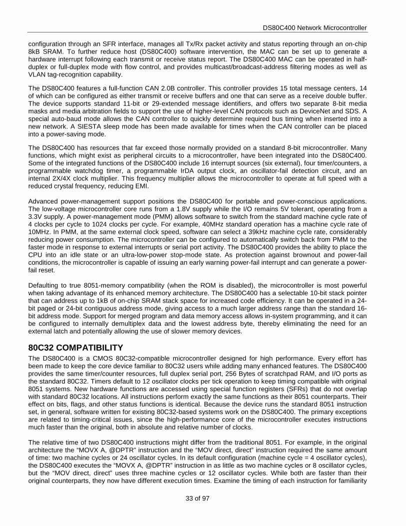
Table 1. SFR Addresses and Bit Locations REGISTER BIT 7 BIT 6 BIT 5 BIT 4 BIT 3 BIT 2 BIT 1 BIT 0 ADDRESS
P4 P4.7/A19 P4.6/A18 P4.5/A17 P4.4/A16 P4.3/CE3 P4.2/CE2 P4.1/CE1 P4.0/CE0 80h SP 81h
DPL 82h DPH 83h DPL1 84h DPH1 85h DPS ID1 ID0 TSL AID SEL1 — — SEL0 86h
PCON SMOD_0 SMOD0 OFDF OFDE GF1 GF0 STOP IDLE 87h TCON TF1 TR1 TF0 TR0 IE1 IT1 IE0 IT0 88h TMOD GATE C/T M1 M0 GATE C/T M1 M0 89h
TL0 8Ah TL1 8Bh TH0 8Ch TH1 8Dh
CKCON WD1 WD0 T2M T1M T0M MD2 MD1 MD0 8Eh P1 P1.7/INT5 P1.6/INT4 P1.5/INT3 P1.4/INT2 P1.3/TXD P1.2/RXD1 P1.1/T2EX P1.0/T2 90h
EXIF IE5 IE4 IE3 IE2 CKRY RGMD RGSL BGS 91h P4CNT — — P4CNT.5 P4CNT.4 P4CNT.3 P4CNT.2 P4CNT.1 P4CNT.0 92h
DPX 93h DPX1 95h
C0RMS0 96h C0RMS1 97h SCON0 SM0/FE_0 SM1_0 SM2_0 REN_0 TB8_0 RB8_0 TI_0 RI_0 98h SBUF0 99h
ESP — — — — — — ESP.1 ESP.0 9Bh AP 9Ch
ACON — — MROM BPME BROM SA AM1 AM0 9Dh C0TMA0 9Eh C0TMA1 9Fh
P2 P2.7/A15 P2.6/A14 P2.5/A13 P2.4/A12 P2.3/A11 P2.2/A10 P2.1/A9 P2.0/A8 A0h P5 P5.7/PCE3 P5.6/PCE2 P5.5/PCE1 P5.4/PCE0 P5.3 P5.2/T3 P5.1/C0RX P5.0/C0TX A1h
P5CNT — CAN0BA — — C0_I/O P5CNT.2 P5CNT.1 P5CNT.0 A2h C0C ERIE STIE PDE SIESTA CRST AUTOB ERCS SWINT A3h C0S BSS EC96/128 WKS RXS TXS ER2 ER1 ER0 A4h C0IR INTIN7 INTIN6 INTIN5 INTIN4 INTIN3 INTIN2 INTIN1 INTIN0 A5h C0TE A6h C0RE A7h
IE EA ES1 ET2 ES0 ET1 EX1 ET0 EX0 A8h SADDR0 A9h SADDR1 AAh C0M1C MSRDY ETI ERI INTRQ EXTRQ MTRQ ROW/TIH DTUP ABh C0M2C MSRDY ETI ERI INTRQ EXTRQ MTRQ ROW/TIH DTUP ACh C0M3C MSRDY ETI ERI INTRQ EXTRQ MTRQ ROW/TIH DTUP ADh C0M4C MSRDY ETI ERI INTRQ EXTRQ MTRQ ROW/TIH DTUP AEh C0M5C MSRDY ETI ERI INTRQ EXTRQ MTRQ ROW/TIH DTUP AFh
P3 P3.7/RD P3.6/WR P3.5/T1 P3.4/T0 P3.3/INT1 P3.2/INT0 P3.1/TXD0 P3.0/RXD0 B0h P6 P6.7/TXD2 P6.6/RXD2 P6.5/A21 P6.4/A20 P6.3/CE7 P6.2/CE6 P6.1/CE5 P6.0/CE4 B1h
P6CNT — — P6CNT.5 P6CNT.4 P6CNT.3 P6CNT.2 P6CNT.1 P6CNT.0 B2h C0M6C MSRDY ETI ERI INTRQ EXTRQ MTRQ ROW/TIH DTUP B3h C0M7C MSRDY ETI ERI INTRQ EXTRQ MTRQ ROW/TIH DTUP B4h C0M8C MSRDY ETI ERI INTRQ EXTRQ MTRQ ROW/TIH DTUP B5h

DS80C400 Network Microcontroller
36 of 97
REGISTER BIT 7 BIT 6 BIT 5 BIT 4 BIT 3 BIT 2 BIT 1 BIT 0 ADDRESS C0M9C MSRDY ETI ERI INTRQ EXTRQ MTRQ ROW/TIH DTUP B6h
C0M10C MSRDY ETI ERI INTRQ EXTRQ MTRQ ROW/TIH DTUP B7h IP — PS1 PT2 PS0 PT1 PX1 PT0 PX0 B8h
SADEN0 B9h SADEN1 BAh C0M11C MSRDY ETI ERI INTRQ EXTRQ MTRQ ROW/TIH DTUP BBh C0M12C MSRDY ETI ERI INTRQ EXTRQ MTRQ ROW/TIH DTUP BCh C0M13C MSRDY ETI ERI INTRQ EXTRQ MTRQ ROW/TIH DTUP BDh C0M14C MSRDY ETI ERI INTRQ EXTRQ MTRQ ROW/TIH DTUP BEh C0M15C MSRDY ETI ERI INTRQ EXTRQ MTRQ ROW/TIH DTUP BFh SCON1 SM0/FE_1 SM1_1 SM2_1 REN_1 TB8_1 RB8_1 TI_1 RI_1 C0h SBUF1 C1h PMR CD1 CD0 SWB CTM 4X/2X ALEOFF — — C4h
STATUS PIP HIP LIP — SPTA1 SPRA1 SPTA0 SPRA0 C5h MCON IDM1 IDM0 CMA — PDCE3 PDCE2 PDCE1 PDCE0 C6h
TA C7h T2CON TF2 EXF2 RCLK TCLK EXEN2 TR2 C/T2 CP/RL2 C8h T2MOD — — — D13T1 D13T2 — T2OE DCEN C9h RCAP2L CAh RCAP2H CBh
TL2 CCh TH2 CDh COR IRDACK — — C0BPR7 C0BPR6 COD1 COD0 CLKOE CEh PSW CY AC F0 RS1 RS0 OV F1 P D0h
MCNT0 LSHIFT CSE SCE MAS4 MAS3 MAS2 MAS1 MAS0 D1h MCNT1 MST MOF SCB CLM — — — — D2h
MA D3h MB D4h MC D5h
MCON1 — — — — PDCE7 PDCE6 PDCE5 PDCE4 D6h MCON2 WPIF WPR2 WPR1 WPR0 WPE3 WPE2 WPE1 WPE0 D7h WDCON SMOD_1 POR EPFI PFI WDIF WTRF EWT RWT D8h SADDR2 D9h
BPA1 DAh BPA2 DBh BPA3 DCh ACC E0h
OCAD E1h CSRD E3h CSRA E4h EBS FPE RBF — BS4 BS3 BS2 BS1 BS0 E5h
BCUD E6h BCUC BUSY EPMF TIF RIF BC3 BC2 BC1 BC0 E7h
EIE EPMIE C0IE EAIE EWDI EWPI ES2 ET3 EX2-5 E8h MXAX EAh DPX2 EBh DPX3 EDh
OWMAD — — — — — A2 A1 A0 EEh OWMDR EFh
B F0h SADEN2 F1h
DPL2 F2h
DS80C400 Network Microcontroller
37 of 97
REGISTER BIT 7 BIT 6 BIT 5 BIT 4 BIT 3 BIT 2 BIT 1 BIT 0 ADDRESS DPH2 F3h DPL3 F4h DPH3 F5h DPS1 ID3 ID2 — — — — — — F6h
STATUS1 — — — — V1PF V3PF SPTA2 SPRA2 F7h EIP EPMIP C0IP EAIP PWDI PWPI PS2 PT3 PX2-5 F8h P7 P7.7/A7 P7.6/A6 P7.5/A5 P7.4/A4 P7.3/A3 P7.2/A2 P7.1/A1 P7.0/A0 F9h TL3 FBh TH3 FCh
T3CM TF3 TR3 T3M SMOD_2 GATE C/T3 M1 M0 FDh SCON2 SM0/FE_2 SM1_2 SM2_2 REN_2 TB8_2 RB8_2 TI_2 RI_2 FEh SBUF2 FFh
Note: Shaded bits are timed-access protected.
DS80C400 Network Microcontroller
38 of 97
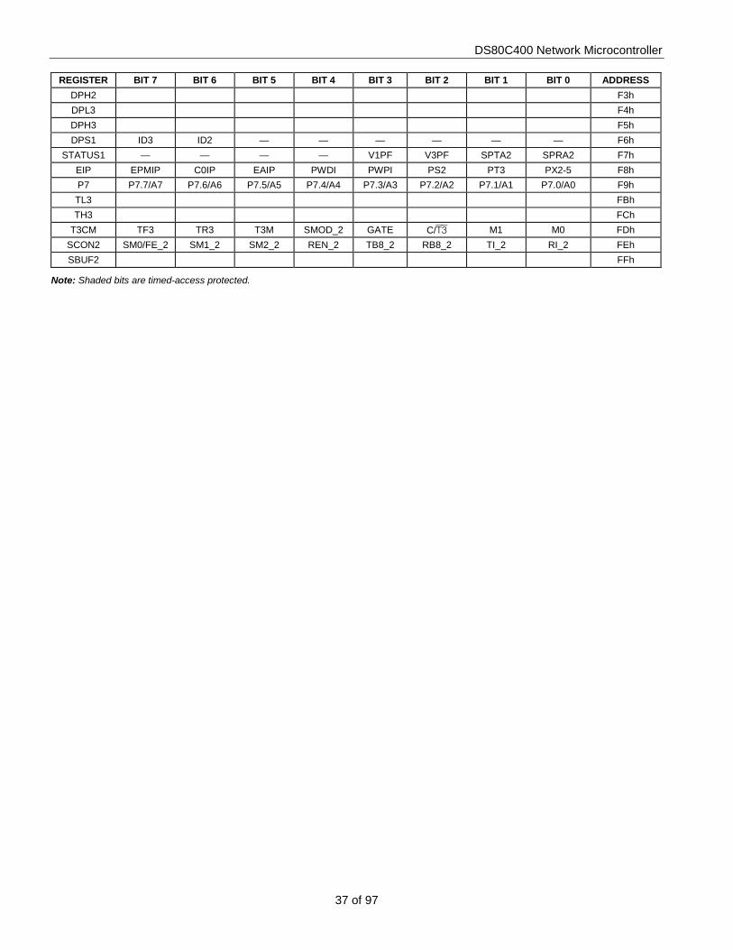
Table 2. SFR Reset Values REGISTER BIT 7 BIT 6 BIT 5 BIT 4 BIT 3 BIT 2 BIT 1 BIT 0 ADDRESS
P4 1 1 1 1 1 1 1 1 80h SP 0 0 0 0 0 0 0 0 81h
DPL 0 0 0 0 0 0 0 0 82h DPH 0 0 0 0 0 0 0 0 83h DPL1 0 0 0 0 0 0 0 0 84h DPH1 0 0 0 0 0 0 0 0 85h DPS 0 0 0 0 0 0 0 0 86h
PCON 0 0 Special 0 0 0 0 0 87h TCON 0 0 0 0 0 0 0 0 88h TMOD 0 0 0 0 0 0 0 0 89h
TL0 0 0 0 0 0 0 0 0 8Ah TL1 0 0 0 0 0 0 0 0 8Bh TH0 0 0 0 0 0 0 0 0 8Ch TH1 0 0 0 0 0 0 0 0 8Dh
CKCON 0 0 0 0 0 0 0 1 8Eh P1 1 1 1 1 1 1 1 1 90h
EXIF 0 0 0 0 Special Special Special 0 91h P4CNT 1 1 1 1 1 1 1 1 92h
DPX 0 0 0 0 0 0 0 0 93h DPX1 0 0 0 0 0 0 0 0 95h
C0RMS0 0 0 0 0 0 0 0 0 96h C0RMS1 0 0 0 0 0 0 0 0 97h SCON0 0 0 0 0 0 0 0 0 98h SBUF0 0 0 0 0 0 0 0 0 99h
ESP 1 1 1 1 1 1 0 0 9Bh AP 0 0 0 0 0 0 0 0 9Ch
ACON 1 1 0 0 Special 0 0 0 9Dh C0TMA0 0 0 0 0 0 0 0 0 9Eh C0TMA1 0 0 0 0 0 0 0 0 9Fh
P2 1 1 1 1 1 1 1 1 A0h P5 1 1 1 1 1 1 1 1 A1h
P5CNT 1 0 0 0 0 0 0 0 A2h C0C 0 0 0 0 1 0 0 1 A3h C0S 0 0 0 0 0 0 0 0 A4h C0IR 0 0 0 0 0 0 0 0 A5h C0TE 0 0 0 0 0 0 0 0 A6h C0RE 0 0 0 0 0 0 0 0 A7h
IE 0 0 0 0 0 0 0 0 A8h SADDR0 0 0 0 0 0 0 0 0 A9h SADDR1 0 0 0 0 0 0 0 0 AAh C0M1C 0 0 0 0 0 0 0 0 ABh C0M2C 0 0 0 0 0 0 0 0 ACh C0M3C 0 0 0 0 0 0 0 0 ADh C0M4C 0 0 0 0 0 0 0 0 AEh C0M5C 0 0 0 0 0 0 0 0 AFh
P3 1 1 1 1 1 1 1 1 B0h P6 1 1 1 1 1 1 1 1 B1h
P6CNT 0 0 0 0 0 0 0 0 B2h C0M6C 0 0 0 0 0 0 0 0 B3h C0M7C 0 0 0 0 0 0 0 0 B4h C0M8C 0 0 0 0 0 0 0 0 B5h C0M9C 0 0 0 0 0 0 0 0 B6h
C0M10C 0 0 0 0 0 0 0 0 B7h IP 1 0 0 0 0 0 0 0 B8h
SADEN0 0 0 0 0 0 0 0 0 B9h SADEN1 0 0 0 0 0 0 0 0 BAh C0M11C 0 0 0 0 0 0 0 0 BBh C0M12C 0 0 0 0 0 0 0 0 BCh C0M13C 0 0 0 0 0 0 0 0 BDh C0M14C 0 0 0 0 0 0 0 0 BEh C0M15C 0 0 0 0 0 0 0 0 BFh SCON1 0 0 0 0 0 0 0 0 C0h SBUF1 0 0 0 0 0 0 0 0 C1h PMR 1 0 0 0 0 0 1 1 C4h

DS80C400 Network Microcontroller
39 of 97
REGISTER BIT 7 BIT 6 BIT 5 BIT 4 BIT 3 BIT 2 BIT 1 BIT 0 ADDRESS STATUS 0 0 0 1 0 0 0 0 C5h MCON 0 0 0 1 0 0 0 0 C6h
TA 1 1 1 1 1 1 1 1 C7h T2CON 0 0 0 0 0 0 0 0 C8h T2MOD 1 1 0 0 0 1 0 0 C9h RCAP2L 0 0 0 0 0 0 0 0 CAh RCAP2H 0 0 0 0 0 0 0 0 CBh
TL2 0 0 0 0 0 0 0 0 CCh TH2 0 0 0 0 0 0 0 0 CDh COR 0 1 1 0 0 0 0 0 CEh PSW 0 0 0 0 0 0 0 0 D0h
MCNT0 0 0 0 0 0 0 0 0 D1h MCNT1 0 0 0 0 1 1 1 1 D2h
MA 0 0 0 0 0 0 0 0 D3h MB 0 0 0 0 0 0 0 0 D4h MC 0 0 0 0 0 0 0 0 D5h
MCON1 1 1 1 1 0 0 0 0 D6h MCON2 0 0 0 0 0 0 0 0 D7h WDCON 0 Special 0 Special 0 Special 0 0 D8h SADDR2 0 0 0 0 0 0 0 0 D9h
BPA1 0 0 0 0 0 0 0 0 DAh BPA2 0 0 0 0 0 0 0 0 DBh BPA3 0 0 0 0 0 0 0 0 DCh ACC 0 0 0 0 0 0 0 0 E0h
OCAD 0 0 0 0 0 0 0 0 E1h CSRD 0 0 0 0 0 0 0 0 E3h CSRA 0 0 0 0 0 0 0 0 E4h EBS 0 1 1 0 0 0 0 0 E5h
BCUD 0 0 0 0 0 0 0 0 E6h BCUC 0 0 0 0 0 0 0 0 E7h
EIE 0 0 0 0 0 0 0 0 E8h MXAX 0 0 0 0 0 0 0 0 EAh DPX2 0 0 0 0 0 0 0 0 EBh DPX3 0 0 0 0 0 0 0 0 EDh
OWMAD 0 0 0 0 0 1 1 1 EEh OWMDR 0 0 0 0 0 0 0 0 EFh
B 0 0 0 0 0 0 0 0 F0h SADEN2 0 0 0 0 0 0 0 0 F1h
DPL2 0 0 0 0 0 0 0 0 F2h DPH2 0 0 0 0 0 0 0 0 F3h DPL3 0 0 0 0 0 0 0 0 F4h DPH3 0 0 0 0 0 0 0 0 F5h DPS1 0 0 1 1 1 1 1 1 F6h
STATUS1 1 1 1 1 1 1 0 0 F7h EIP 0 0 0 0 0 0 0 0 F8h P7 1 1 1 1 1 1 1 1 F9h TL3 0 0 0 0 0 0 0 0 FBh TH3 0 0 0 0 0 0 0 0 FCh
T3CM 0 0 0 0 0 0 0 0 FDh SCON2 0 0 0 0 0 0 0 0 FEh SBUF2 0 0 0 0 0 0 0 0 FFh
Note: Shaded bits are timed-access protected. “Special” bits are affected only by certain types of reset. Refer to the user’s guide for details.

DS80C400 Network Microcontroller
40 of 97
TIMED-ACCESS PROTECTION Selected SFR bits are critical to operation, making it desirable to protect them against an accidental write operation. The timed-access procedure prevents errant behavior from accidentally altering bits that would seriously affect microcontroller operation. The timed-access procedure requires that the write of a protected bit be immediately preceded by the following two instructions:
MOV 0C7h, #0AAh MOV 0C7h, #55h
Writing an AAh followed by a 55h to the timed access register (location C7h), opens a three-cycle window that allows software to modify one of the protected bits. The protected bits are:
SFR BIT(S) NAME FUNCTION EXIF (91h) EXIF.0 BGS Bandgap Select
P4CNT (92h) P4CNT.5–0 — Port 4 Pin Configuration Control Bits ACON (9Dh) ACON.5 MROM Merge ROM
— ACON.4 BPME Breakpoint Mode Enable — ACON.3 BROM By-Pass ROM — ACON.2 SA Stack Address Mode — ACON.1–0 AM1–AM0 Address Mode Select Bits
P5CNT (A2h) P5CNT.2–0 — Port 5 Pin Configuration Control Bits C0C (A3h) C0C.3 CRST CAN 0 Reset
P6CNT (B2h) P6CNT.5–0 — Port 6 Pin Configuration Control Bits MCON (C6h) MCON.7–6 IDM1–IDM0 Internal Memory Configuration Bits
— MCON.5 CAN CMA Data Memory Assignment — MCON.3–0 PDCE3–PDCE0 Program/Data-Chip Enables
COR (CEh) COR.7 IRDACK IRDA Clock-Output Enable — COR.4–3 C0BPR7–C0BPR6 CAN 0 Baud Rate Prescale Bits — COR.2–1 COD1–COD0 CAN Clock-Output Divide Bits — COR.0 CLKOE CAN Clock-Output Enable
MCON1 (D6h) MCON1.3–0 PDCE7–PDCE4 Program/Data Chip Enable MCON2 (D7h) MCON2.6–4 WPR2–WPR0 Write-Protect Range Bits
MCON2.3–0 WPE3–WPE0 Write-Protect Enable Bits WDCON (D8h) WDCON.6 POR Power-On Reset Flag
— WDCON.3 WDIF Watchdog Interrupt Flag — WDCON.1 EWT Watchdog Reset Enable — WDCON.0 RWT Reset Watchdog Timer
EBS (E5h) EBS.7 FPE Flush Filter Failed-Packet Enable — EBS.4–0 BS4-BS0 Buffer Size Configuration Bits
MEMORY ARCHITECTURE The DS80C400 incorporates four internal memory areas: • 256 Bytes of scratchpad (or direct) RAM • 8kB of SRAM for Ethernet MAC transmit/receive buffer memory • 1kB of SRAM configurable as various combinations of data memory and stack memory • 256 Bytes of RAM reserved for the CAN message centers • 64kB embedded ROM firmware Up to 16MB of external code memory can be addressed through a multiplexed or demultiplexed 22-bit address bus/8-bit data bus through eight available chip enables. Up to 4MB of external data memory can be accessed over the same address/data buses through peripheral-enable signals. The DS80C400 also permits a 16MB merged program/data memory map.

DS80C400 Network Microcontroller
41 of 97
ADDRESSING MODES Three different addressing modes are supported, as selected by the AM1, AM0 bits in the address control (ACON; 9Dh) SFR.
AM1:0 ADDRESS MODE 00b 16-bit (default when ROM disabled) 01b 24-bit paged 1xb 24-bit contiguous (default when ROM enabled)
16-Bit Address Mode The 16-bit address mode accesses memory in a similar manner as a traditional 8051. It is op-code compatible with the 8051 microprocessor and identical to the byte and cycle count of the Maxim high-speed microcontroller family. A device operating in this mode can access up to 64kB of program and data memory. The DS80C400 defaults to this mode following any reset. 24-Bit Paged Address Mode The 24-bit paged address mode retains binary-code compatibility with the 8051 instruction set, but adds one machine cycle to the ACALL, LCALL, RET, and RETI instructions with respect to the Maxim high-speed microcontroller family timing. This is transparent to standard 8051 compilers. Interrupt latency is also increased by one machine cycle. In this mode, interrupt vectors are fetched from 0000xxh. 24-Bit Contiguous Address Mode The 24-bit contiguous addressing mode uses a full 24-bit program counter, and all modified branching instructions automatically save and restore the entire program counter. The 24-bit branching instructions such as ACALL, AJMP, LCALL, LJMP, MOV DPTR, RET, and RETI instructions require an assembler, compiler, and linker that specifically supports these features. The INC DPTR is lengthened by one cycle but remains byte-count compatible with the standard 8051 instruction set. Visit www.maxim-ic.com/microcontrollers for a list of tools that support the DS80C400. Extended Address Generation
FUNCTION ADDRESS BITS 23–16 ADDRESS BITS 15–8 ADDRESS BITS 7–0
MOVX Instructions Using DPTRn DPXn DPHn DPLn
MOVX Instructions Using @Ri MXAX;EAh P2;A0h Ri
Addressing Program Memory In 24-Bit Paged Mode AP;9Ch — —
10-Bit Stack Pointer Mode — ESP;9Bh SP;81h
External Program Memory Addressing Since the DS80C400 is not bound to the 8051’s traditional 16-bit address mode, on-chip hardware enhancements were made to accommodate the larger memory interfaces associated with 24-bit addressing. The DS80C400 provides SFR bits to configure certain port pins as upper address lines and chip enables. The Port 4 control register (P4CNT; 92h) and Port 6 control register (P6CNT; B2h) control the number of chip enables that are used and the maximum amount of program memory that can be accessed per chip enable. Tables 3 and 4 illustrate which port pins are converted to address lines or chip enables as a result of the P4CNT and P6CNT bit settings.

DS80C400 Network Microcontroller
42 of 97
Table 3. Extended Address Generation P4CNT.5–3 P6.5 P6.4 P4.7 P4.6 P4.5 P4.4 MAX MEMORY ACCESSIBLE
per CE 000 I/O I/O I/O I/O I/O I/O 32kB (Note 1) 001 I/O I/O I/O I/O I/O A16 128kB 010 I/O I/O I/O I/O A17 A16 256kB 011 I/O I/O I/O A18 A17 A16 512kB 100 I/O I/O A19 A18 A17 A16 1MB 101 I/O A20 A19 A18 A17 A16 2MB (Note 2)
110 or 111 (default) A21 A20 A19 A18 A17 A16 4MB (Note 3) Table 4. Chip-Enable Generation
P6CNT.2–0 PORT 6 PIN FUNCTION
P4CNT.2–0 PORT 4 PIN FUNCTION
P6.3 P6.2 P6.1 P6.0 P4.3 P4.2 P4.1 P4.0 000 (default)
(Note 2) I/O I/O I/O I/O 000 I/O I/O I/O I/O
100 I/O I/O I/O CE4 100 I/O I/O I/O CE0 101 I/O I/O CE5 CE4 101 I/O I/O CE1 CE0 110 I/O CE6 CE5 CE4 110 I/O CE2 CE1 CE0
111 (Note 2) CE7 CE6 CE5 CE4 111 (default) CE3 CE2 CE1 CE0
Note 1: Only 32kB of memory is accessible per chip enable for the P4CNT.5-3 = 000b setting, which means at least two chip enables are needed to address the standard 16-bit (0–FFFFh) address range.
Note 2: When the ROM is enabled, the default memory map is reconfigured to 2MB per CE, P4CNT.5-3 = 101b, and CE4–CE7 are enabled, P6CNT.2-0 = 111b.
Note 3: The default P4CNT.5-3 = 111b setting (4MB accessible per CE) requires only four chip enables to access the maximum 24-bit (0–FFFFFFh) address range.
External Data Memory Addressing Using a similar implementation as was used to expand program memory access, the DS80C400 allows up to 4MB of data memory access through four peripheral chip enables (PCE). The Port 5 control register (P5CNT; A2h) and Port 6 control register (P6CNT; B2h) designate the number of peripheral chip enables and the maximum amount of addressable data memory per peripheral chip enable. Table 5 shows which port pins are converted to peripheral chip enables, along with the maximum memory accessible through each peripheral chip enable for P5CNT, P6CNT bit settings. Table 5. Peripheral Chip-Enable Generation
P5CNT.2–0 P5.7 P5.6 P5.5 P5.4 P6CNT.5–3 MAX MEMORY ACSESSIBLE per PCE 000 (default) I/O I/O I/O I/O 000 (default) 32kB
100 I/O I/O I/O PCE0 001 128kB 101 I/O I/O PCE1 PCE0 010 256kB 110 I/O PCE2 PCE1 PCE0 011 512kB 111 PCE3 PCE2 PCE1 PCE0 100 1MB
Demultiplexed External Memory Addressing On power-up or following any reset, the DS80C400 defaults to the traditional 8051 external memory interface, with the address MSB presented on Port 2 and the address LSB and data multiplexed on Port 0. The multiplexed mode requires an external latch to demultiplex the address LSB and data. The DS80C400 provides an external pin (MUX) that, when pulled high during a power-on reset, demultiplexes the address LSB and data. If demultiplexed mode is enabled, the address LSB is provided on Port 7 and the data on Port 0. At the expense of consuming Port 7, demultiplexed mode eliminates the external demultiplexing latch and the delay element associated with the latch. In some cases, the removal of this timing delay allows use of slower, less expensive external memory devices. Table 6 shows pin assignments for the multiplexed (traditional 8051) and demultiplexed external addressing modes.
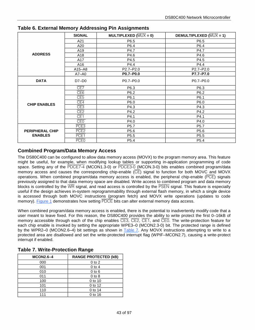
DS80C400 Network Microcontroller
43 of 97
Table 6. External Memory Addressing Pin Assignments
ADDRESS
SIGNAL MULTIPLEXED (MUX = 0) DEMULTIPLEXED (MUX = 1) A21 P6.5 P6.5 A20 P6.4 P6.4 A19 P4.7 P4.7 A18 P4.6 P4.6 A17 P4.5 P4.5 A16 P4.4 P4.4
A15–A8 P2.7–P2.0 P2.7–P2.0 A7–A0 P0.7–P0.0 P7.7–P7.0
DATA D7–D0 P0.7–P0.0 P0.7–P0.0
CHIP ENABLES
CE7 P6.3 P6.3 CE6 P6.2 P6.2 CE5 P6.1 P6.1 CE4 P6.0 P6.0 CE3 P4.3 P4.3 CE2 P4.2 P4.2 CE1 P4.1 P4.1 CE0 P4.0 P4.0
PERIPHERAL CHIP ENABLES
PCE3 P5.7 P5.7 PCE2 P5.6 P5.6 PCE1 P5.5 P5.5 PCE0 P5.4 P5.4
Combined Program/Data Memory Access The DS80C400 can be configured to allow data memory access (MOVX) to the program memory area. This feature might be useful, for example, when modifying lookup tables or supporting in-application programming of code space. Setting any of the PDCE7-4 (MCON1.3-0) or PDCE3-0 (MCON.3-0) bits enables combined program/data memory access and causes the corresponding chip-enable (CE) signal to function for both MOVC and MOVX operations. When combined program/data memory access is enabled, the peripheral chip-enable (PCE) signals previously assigned to that data memory space are disabled. Write access to combined program and data memory blocks is controlled by the WR signal, and read access is controlled by the PSEN signal. This feature is especially useful if the design achieves in-system reprogrammability through external flash memory, in which a single device is accessed through both MOVC instructions (program fetch) and MOVX write operations (updates to code memory). Figure 1 demonstrates how setting PDCE bits can alter external memory data access. When combined program/data memory access is enabled, there is the potential to inadvertently modify code that a user meant to leave fixed. For this reason, the DS80C400 provides the ability to write protect the first 0–16kB of memory accessible through each of the chip enables CE3, CE2, CE1, and CE0. The write-protection feature for each chip enable is invoked by setting the appropriate WPE3–0 (MCON2.3-0) bit. The protected range is defined by the WPR2–0 (MCON2.6–4) bit settings as shown in Table 7. Any MOVX instructions attempting to write to a protected area are disallowed and set the write-protected interrupt flag (WPIF–MCON2.7), causing a write-protect interrupt if enabled. Table 7. Write-Protection Range
MCON2.6–4 RANGE PROTECTED (kB) 000 0 to 2 001 0 to 4 010 0 to 6 011 0 to 8 100 0 to 10 101 0 to 12 110 0 to 14 111 0 to 16

DS80C400 Network Microcontroller
44 of 97
Figure 1. Example External Memory Map—Merged Program/Data Enhanced Quad Data Pointers The DS80C400 offers enhanced features for accelerating the access and movement of data. It contains four data pointers (DPTR0, DPTR1, DPTR2, and DPTR3), in comparison to the single data pointer offered on the original 8051, and allows the user to define, for each data pointer, whether the INC DPTR instruction increments or decrements the selected pointer. Also, realizing that many data accesses occur in large contiguous blocks, the DS80C400 can be configured to automatically increment or decrement a data pointer on execution of certain instructions. This improvement greatly speeds access to consecutive pieces of data since hardware can now accomplish a task (advancing the data pointer) that previously required software execution time. Finally, each pair of data pointers (DPTR0, DPTR1 or DPTR2, DPTR3) can be configured for an auto-toggle mode. When placed into this mode, certain data pointer-related instructions toggle the active data-pointer selection to the other pointer in the pair. Enabling the auto-toggle feature, with one pointer to source data and a second pointer to destination data, greatly speeds the copying of large data blocks. DPTR0 is located at the same address as the original 8051 data pointer, allowing the DS80C400 to execute standard 8051 code with no modifications. The registers making up the second, third, and fourth data pointers are located at SFR address locations not used in the original 8051. To access the extended 24-bit address range supported by the DS80C400, a third, high-order byte (DPXn) has been added to each pointer so that each data pointer is now composed of the SFR combination DPXn+DPHn+DPLn. Table 8 summarizes the SFRs that make up each data pointer.
CE0 =2M x 8 PCE0 = 1M x 8
PCE1 = 1M x 8 PCE2 = 1M x 8
PCE3 = 1M x 8 CE1 =2M x 8
CE7 = 2M x 8
CE6 = 2M x 8
CE5 = 2M x 8
CE4 = 2M x 8
CE3 = 2M x 8
CE2 =2M x 8
PROGRAM MEMORY
DATA MEMORY
N
ON
AD
DR
ESSA
BLE
CE0 = 2M x 8
PCE2 = 1M x 8
PCE3 = 1M x 8 CE1 = 2M x 8
CE7 = 2M x 8
CE6 = 2M x 8
CE5 = 2M x 8
CE4 = 2M x 8
CE3 = 2M x 8
CE2 = 2M x 8
PROGRAM MEMORY
DATA MEMORY
N
ON
AD
DR
ESSA
BLE
PROGRAM/ DATA
MEMORY
PDCE3 = 1
PDCE0 = 1
BEFORE AFTER
DS80C400 Network Microcontroller
45 of 97
Table 8. Data Pointer SFR Locations DATA POINTER DPX+DPH+DPL COMBINATION
DPTR0 DPX (93h) + DPH (83h) + DPL (82h) DPTR1 DPX1 (95h) + DPH1 (85h) + DPL1 (84h) DPTR2 DPX2 (EBh) + DPH2 (F3h) + DPL2 (F2h) DPTR3 DPX3 (EDh) + DPH3 (F5h) + DPL3 (F4h)
The active data pointer is selected with the data pointer select bits SEL1 (DPS.3) and SEL (DPS.0). For the SEL1 and SEL bits, the 00b state selects DPTR0, 01b selects DPTR1, 10b selects DPTR2, and 11b selects DPTR3. Any instructions that reference the DPTR (i.e., MOVX A, @DPTR) use the data pointer selected by the SEL1, SEL bit-pair combination. To allow for code compatibility with previous dual data pointer microcontrollers, the bits adjacent to SEL are not implemented so that the INC DPS instruction can still be used to quickly toggle between DPTR0 and DPTR1 or between DPTR2 and DPTR3. Unlike the standard 8051, the DS80C400 has the ability to decrement as well as increment the data pointers without additional instructions. Each data pointer (DPTR0, DPTR1, DPTR2, DPTR3) has an associated control bit (ID0, ID1, ID2, ID3) that determines whether the INC DPTR operation results in an increment or decrement of the pointer. When the active data pointer ID (increment/decrement) control bit is clear, the INC DPTR instruction increments the pointer, whereas a decrement occurs if the active pointer’s ID bit is set when the INC DPTR instruction is performed. ID0 = DPS.6 ID1 = DPS.7 ID2 = DPS1.6 ID3 = DPS1.7 Another useful feature of the device is its ability to automatically switch the active data pointer after certain DPTR-based instructions are executed. This feature can greatly reduce the software overhead associated with data memory block moves, which toggle between the source and destination registers. The auto-toggle feature does not toggle between all four data pointers, nor does it allow the user to select which data pointers to toggle between. When the toggle select bit (TSL;DPS.5) is set to 1, the SEL bit (DPS.0) is automatically toggled every time one of the DPTR instructions below is executed. Thus, depending upon the state of the SEL1 bit (DPS.3), the active data pointer toggles the DPTR0, DPTR1 pair or the DPTR2, DPTR3 pair. Auto-Toggle (if TSL = 1) INC DPTR MOV DPTR, #data16 MOV DPTR, #data24 MOVC A, @A+DPTR MOVX A, @DPTR MOVX @DPTR, A As a brief example, if TSL is set to 1, then both data pointers can be updated with two INC DPTR instructions. Assume that SEL1 = 0 and SEL = 0, making DPTR0 the active data pointer. The first INC DPTR increments DPTR0 and toggles SEL to 1. The second instruction increments DPTR1 and toggles SEL back to 0. INC DPTR INC DPTR As a further enhancement, the DS80C400 provides the ability to automatically increment/decrement the active data pointer after certain DPTR-based instructions are executed. Copying large blocks of data generally requires that the source and destination pointers index byte-by-byte through their respective data ranges. The traditional method for incrementing each pointer is by using the INC DPTR instruction. When the auto-increment/decrement bit (AID:DPS.4) is set to 1, the active data pointer is automatically incremented or decremented every time one of the DPTR instructions below is executed.

DS80C400 Network Microcontroller
46 of 97
Auto-Increment/Decrement (if AID = 1) MOVC A, @A+DPTR MOVX A, @DPTR MOVX @DPTR, A When used in conjunction, the auto-toggle and auto-increment/decrement features can produce very fast and efficient routines for copying or moving data. For example, suppose you want to copy three bytes of data from a source location (pointed to by DPTR2) to a destination location (pointed to by DPTR3). Assuming that DPTR2 is the active pointer (SEL1 = 1, SEL = 0), with TSL = 1 and AID = 1, the instruction sequence below copies the three bytes: MOVX A, @DPTR MOVX @DPTR, A MOVX A, @DPTR MOVX @DPTR, A MOVX A, @DPTR MOVX @DPTR, A Stretch Memory Cycles The DS80C400 allows user-application software to select the number of machine cycles it takes to execute a MOVX instruction, allowing access to both fast and slow off-chip data memory and/or peripherals without glue logic. High-speed systems often include memory-mapped peripherals such as LCDs or UARTs with slow access times, so it may not be necessary or desirable to access external devices at full speed. The microprocessor can perform a MOVX instruction in as little as two machine cycles or as many as 12 machine cycles. Accesses to internal MOVX SRAM always use two cycles. Note that stretch cycle settings affect external MOVX memory operations only and there is no way to slow the accesses to program memory other than to use a slower crystal (or external clock). External MOVX timing is governed by the selection of 0-to-7 stretch cycles, controlled by the MD2–MD0 SFR bits in the clock control register (CKCON.2–0). A stretch of 0 results in a 2-machine cycle MOVX instruction. A stretch of 7 results in a MOVX of 12 machine cycles. Software can dynamically change the stretch value depending on the particular memory or peripheral being accessed. The default of one stretch cycle allows the use of commonly available SRAMs without dramatically lengthening the memory access times. Stretch cycle settings affect external MOVX timing in three gradations. Changing the stretch value from 0 to 1 adds an additional clock cycle each to the data setup and hold times. Stretch values of 2 and 3 each stretch the WR or RD signal by an additional machine cycle. When a stretch value of 4 or above is selected, the interface timing changes dramatically to allow for very slow peripherals. First, the ALE signal is lengthened by one machine cycle. This increases the address setup time into the peripheral by this amount. Next, the address is held on the bus for one additional machine cycle, increasing the address hold time by this amount. The WR and RD signals are then lengthened by a machine cycle. Finally, during a MOVX write the data is held on the bus for one additional machine cycle, thereby increasing the data hold time by this amount. For every stretch value greater than 4, the setup and hold times remain constant, and only the width of the read or write signal is increased. These three gradations are reflected in the AC Electrical Characteristics section, where the eight MOVX timing specifications are represented by only three timing diagrams. The reset default of one stretch cycle results in a three-cycle MOVX for any external access. Therefore, the default off-chip RAM access is not at full speed. This is a convenience to existing designs that use slower RAM. When maximum speed is desired, software should select a stretch value of 0. When using very slow RAM or peripherals, the application software can select a larger stretch value. The specific timing of MOVX instructions as a function of stretch settings is provided in the Electrical Specifications section of this data sheet. As an example, Table 9 shows the read and write strobe widths corresponding to each stretch value.

DS80C400 Network Microcontroller
47 of 97
Table 9. Data Memory Cycle Stretch Values
MD2 MD1 MD0 STRETCH VALUE
MOVX MACHINE CYCLES
APPROXIMATE RD, WR PULSE WIDTH (IN OSCILLATOR CLOCKS)
(4X/2X = 1 CD1:0 = 00)
(4X/2X = 0 CD1:0 = 00)
(4X/2X = X CD1:0 = 10)
(4X/2X = X CD1:0 = 11)
0 0 0 0 (Note 1) 2 0.5 tCLK 1 tCLK 2 tCLK 512 tCLK 0 0 1 1 (Note 2) 3 1 tCLK 2 tCLK 4 tCLK 1024 tCLK 0 1 0 2 4 2 tCLK 4 tCLK 8 tCLK 2048 tCLK 0 1 1 3 5 3 tCLK 6 tCLK 12 tCLK 3072 tCLK 1 0 0 4 9 4 tCLK 8 tCLK 16 tCLK 4096 tCLK 1 0 1 5 10 5 tCLK 10 tCLK 20 tCLK 5120 tCLK 1 1 0 6 11 6 tCLK 12 tCLK 24 tCLK 6144 tCLK 1 1 1 7 12 7 tCLK 14 tCLK 28 tCLK 7168 tCLK
Note 1: All internal MOVX operations execute at the 0 stretch setting. Note 2: Default stretch setting for external MOVX operations following reset, but reset before execution of ROM startup code. Internal MOVX SRAM The DS80C400 contains 9kB of SRAM that is physically divided into a 1kB block and an 8kB block. The 1kB block can be used to support the extended stack-pointer function or can be used as general-purpose MOVX data memory. The 8kB block is used by the Ethernet MAC as frame-buffer memory for incoming or outgoing packet data and can, at the same time, be accessed by the DS80C400 as MOVX data memory. While the MAC is in use, special care should be taken by user software to prevent undesirable MOVX writes from corrupting frame-buffer memory. The address mapping of the 1kB block and the 8kB block are governed by the internal data-memory configuration bits (IDM1, IDM0) in the memory control register (MCON;C6h). Note that when the SA bit (ACON.2) is set, 1kB of the MOVX data memory is accessed by the 10-bit expanded stack pointer. Changing the IDM1:0 configuration bits while SA = 1 does not disrupt the extended stack-pointer function. Internal MOVX memory accesses do not generate WR or RD strobes. The DS80C400 contains an additional 256 Bytes of internal SRAM that is used to configure and operate the 15 CAN-controller message centers. The address location of this 256-Byte block is determined by the CAN data-memory assignment bit (CMA) in the memory control register (MCON; C6h). Table 10. Internal MOVX SRAM Configuration
IDM1 IDM0 CMA 8kB BLOCK (MAC/MOVX DATA)
1kB BLOCK (STACK/MOVX DATA)
256-BYTE (CAN DATA MEMORY)
0 0 0 00E000h–00FFFFh 00DC00h–00DFFFh 00DB00h–00DBFFh 0 0 1 00E000h–00FFFFh 00DC00h–00DFFFh FFDB00h–FFDBFFh 0 1 0 000000h–001FFFh 002000h–0023FFh 00DB00h–00DBFFh 0 1 1 000000h–001FFFh 002000h–0023FFh FFDB00h–FFDBFFh 1 0 0 FFE000h–FFFFFFh FFDC00h–FFDFFFh 00DB00h–00DBFFh 1 0 1 FFE000h–FFFFFFh FFDC00h–FFDFFFh FFDB00h–FFDBFFh
Extended Stack Pointer The DS80C400 supports both the traditional 8-bit and an extended 10-bit stack pointer that improves the performance of large programs written in high-level languages such as C. To enable the 10-bit stack pointer, set the stack-address mode bit, SA (ACON.2). The bit is cleared following a reset, forcing the device to use an 8-bit stack located in the scratchpad RAM area. When the SA bit is set, the device addresses up to 1kB of internal MOVX memory for stack purposes. The 10-bit stack pointer address is generated by concatenating the lower two bits of the extended stack pointer (ESP;9Bh) and the traditional 8051 stack pointer (SP;81h). On-Chip Arithmetic Accelerator An on-chip math accelerator allows the microcontroller to perform 32-bit and 16-bit multiplication, division, shifting, and normalization using dedicated hardware. Math operations are performed by sequentially loading three special registers. The mathematical operation is determined by the sequence in which three dedicated SFRs (MA, MB, and MCNT0) are accessed, eliminating the need for a special step to choose the operation. The normalize function

DS80C400 Network Microcontroller
48 of 97
facilitates the conversion of 4-Byte unsigned binary integers into floating point format. Table 11 shows the operations supported by the math accelerator and their time of execution. Table 11. Arithmetic Accelerator Execution Times
OPERATION RESULT EXECUTION TIME 32-Bit/16-Bit Divide 32-Bit Quotient, 16-Bit Remainder 36 tCLCL 16-Bit/16-Bit Divide 16-Bit Quotient, 16-Bit Remainder 24 tCLCL
16-Bit/16-Bit Multiply 32-Bit Product 24 tCLCL 32-Bit Shift Left/Right 32-Bit Result 36 tCLCL
32-Bit Normalize 32-Bit Mantissa, 5-Bit Exponent 36 tCLCL Table 12 demonstrates the procedure to perform mathematical operations using the hardware math accelerator. The MA and MB registers must be loaded and read in the order shown for proper operation, although accesses to any other registers can be performed between accesses to the MA or MB registers. An access to the MA, MB, or MC registers out of sequence corrupt the operation, requiring the software to clear the MST bit to restart the math accelerator state machine. See the descriptions of the MCNT0 and MCNT1 SFRs for details about how the shift and normalize functions operate. Table 12. Arithmetic Accelerator Sequencing
DIVIDE (32/16 or 16/16) MULTIPLY (16 x 16)
Load MA with dividend LSB. Load MA with dividend LSB + 1*. Load MA with dividend LSB + 2*. Load MA with dividend MSB. Load MB with divisor LSB. Load MB with divisor MSB. Poll the MST bit until cleared. (9 machine cycles for 32-bit numerator) (6 machine cycles for 16-bit numerator) Read MA to retrieve the quotient MSB. Read MA to retrieve the quotient LSB + 2*
Read MA to retrieve the quotient LSB + 1* Read MA to retrieve the quotient LSB. Read MB to retrieve the remainder MSB. Read MB to retrieve the remainder LSB.
Load MB with multiplier LSB. Load MB with multiplier MSB. Load MA with multiplicand LSB. Load MA with multiplicand MSB. Poll the MST bit until cleared (6 machine cycles). Read MA for product MSB. Read MA for product LSB + 2. Read MA for product LSB + 1. Read MA for product LSB.
SHIFT RIGHT/LEFT NORMALIZE Load MA with data LSB. Load MA with data LSB + 1. Load MA with data LSB + 2. Load MA with data MSB. Configure MCNT0/MCNT1 registers as required. Poll the MST bit until cleared (9 machine cycles). Read MA for result MSB. Read MA for result LSB + 2. Read MA for result LSB + 1. Read MA for result LSB.
Load MA with data LSB. Load MA with data LSB + 1. Load MA with data LSB + 2. Load MA with data MSB. Configure MCNT0.4–0 = 00000b. Poll the MST bit until cleared (9 machine cycles). Read MA for mantissa MSB. Read MA for mantissa LSB + 2. Read MA for mantissa LSB + 1. Read MA for mantissa LSB. Read MCNT0.4–MCNT0.0 for exponent.
*Not performed for 16-bit numerator.
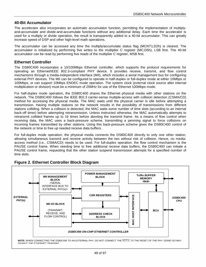
DS80C400 Network Microcontroller
49 of 97
40-Bit Accumulator The accelerator also incorporates an automatic accumulator function, permitting the implementation of multiply-and-accumulate and divide-and-accumulate functions without any additional delay. Each time the accelerator is used for a multiply or divide operation, the result is transparently added to a 40-bit accumulator. This can greatly increase speed of DSP and other high-level math operations.
The accumulator can be accessed any time the multiply/accumulate status flag (MCNT1;D2h) is cleared. The accumulator is initialized by performing five writes to the multiplier C register (MC;D5h), LSB first. The 40-bit accumulator can be read by performing five reads of the multiplier C register, MSB first. Ethernet Controller The DS80C400 incorporates a 10/100Mbps Ethernet controller, which supports the protocol requirements for operating an Ethernet/IEEE 802.3-compliant PHY device. It provides receive, transmit, and flow control mechanisms through a media-independent interface (MII), which includes a serial management bus for configuring external PHY devices. The MII can be configured to operate in half-duplex or full-duplex mode at either 10Mbps or 100Mbps, or can support 10Mbps ENDEC mode operation. The system clock (external clock source after internal multiplication or division) must be a minimum of 25MHz for use of the Ethernet 100Mbps mode.
For half-duplex mode operation, the DS80C400 shares the Ethernet physical media with other stations on the network. The DS80C400 follows the IEEE 802.3 carrier-sense multiple-access with collision detection (CSMA/CD) method for accessing the physical media. The MAC waits until the physical carrier is idle before attempting a transmission. Having multiple stations on the network results in the possibility of transmissions from different stations colliding. When a collision is detected, the MAC waits some number of time slots (according to an internal back-off timer) before attempting retransmission. Unless instructed otherwise, the MAC automatically attempts to retransmit collided frames up to 16 times before aborting the transmit frame. As a means of flow control when receiving data, the MAC uses a back-pressure scheme, transmitting a jamming signal to force collisions on incoming frames transmitted by other stations. Using this back-pressure scheme gives the DS80C400 control of the network or time to free up needed receive data buffers.
For full-duplex mode operation, the physical media connects the DS80C400 directly to only one other station, allowing simultaneous transmit and receive activity between the two without risk of collision. Hence, no media-access method (i.e., CSMA/CD) needs to be used. For full-duplex operation, the flow control mechanism is the PAUSE control frame. When needing time to free additional receive data buffers, the DS80C400 can initiate a PAUSE control frame, requesting that the other station suspend transmission attempts for a specified number of time slots. Figure 2. Ethernet Controller Block Diagram
MII MANAGEMENT BLOCK
<SERIAL INTERFACE BUS TO EXTERNAL PHY(s)>
MII I/O BLOCK
(TRANSMIT, RECEIVE, AND
FLOW CONTROL)
CSR REGISTERS
ADDRESS CHECK
BLOCK
POWER MANAGEMENT BLOCK
MA
C H
OST
INTE
RFA
CE
BCU
Tx/Rx BUFFER MEMORY
(8kB)
EXTERNAL PHY(s)
DS80C400 ON-CHIP ETHERNET CONTROLLER
DS80C400 CPU
NOTE: WHEN CONNECTING THE DS80C400 TO AN EXTERNAL PHY, DO NOT CONNECT THE RSTOL TO THE RESET OF THE PHY. DOING SO MAY DISABLE THE ETHERNET TRANSMIT.
DS80C400 Network Microcontroller
50 of 97
Buffer Control Unit The buffer control unit (BCU) serves as the central controller of all DS80C400 Ethernet activity. The BCU regulates CPU read/write activity to the Ethernet controller blocks through a series of SFRs: BCU control (BCUC; E7h), BCU data (BCUD; E6h), CSR address (CSRA; E4h), and CSR data (CSRD; E3h). These SFRs allows the CPU to issue commands to the BCU, exchange packet size/location information with the BCU, configure the on-chip Ethernet MAC, and even communicate with external PHYs through the MII serial-management bus. Table 13 outlines the commands that can be issued through the BCUC register. Prior to issuing a write (1000b) or read (1001b) CSR register command, the CSRA SFR must be configured to address a valid CSR register. For each CSR register write, the CSRD SFR must be loaded with the data to be written prior to issuing the write command, whereas on a read, CSRD returns the CSR register data following the read command. Table 14 lists the CSR register addresses and functions. Table 13. Buffer Control Unit Commands
COMMAND (BCUC.3:BCUC.0) OPERATION
0000 No Operation (default) 0010 Invalidate Current Receive Packet 0011 Flush Receive Buffer 0100 Transmit Request (normal) 0101 Transmit Request (disable padding) 0110 Transmit Request (disable CRC) 1000 Write CSR Register 1001 Read CSR Register 1100 Enable Sleep Mode 1101 Disable Sleep Mode Other Reserved
Table 14. CSR Registers
CSR REGISTER ADDRESS (CSRA) FUNCTION
00h MAC Control 04h Ethernet MAC Physical Address [47:32] 08h Ethernet MAC Physical Address [31:0] 0Ch Multicast Address Hash Table [63:32] 10h Multicast Address Hash Table [31:0] 14h MII Address 18h MII Data 1Ch Flow Control 20h VLAN1 Tag 24h VLAN2 Tag 28h Wake-Up Frame Filter 2Ch Wake-Up Events Control and Status
Other Reserved The BCU is responsible for coordinating and reporting status for all data-packet transactions between the Ethernet MAC and the 8kB packet-buffer memory. The size of the transmit and receive buffers within the 8kB packet-buffer memory is user-configurable through the EBS (E5h) register. During transmit and receive operations, the BCU operates according to the user-defined buffer allocation and tracks consumption of receive buffer memory so that a receive-buffer-full condition can be signaled. For a receive operation, the BCU first must assess whether there are any open pages in receive buffer memory to accommodate an incoming packet. If there are not open pages, the receive-buffer-full (RBF; EBS.6) flag is set. Until the RBF condition is cleared, all incoming frames are missed. If receive buffer memory has open pages, the received data is stored in the first open page starting at byte offset 4, leaving the first 4 bytes open for packet status reporting. Receive packets requiring multiple pages are stored in consecutive pages. Note that the receive buffer operates as a circular queue, with page 0 being the consecutive page to follow the final (n - 1) receive buffer page. The BCU stores incoming data to receive buffer memory until the transaction is complete or until the reception is
DS80C400 Network Microcontroller
51 of 97
aborted. The BCU incorporates a 31 x 8 first-in-first-out receive packet register (receive FIFO) so that the CPU can access information for the next receive packet in queue. Upon reception of each valid packet into receive buffer memory, the BCU writes a receive status word into the first word of the receive packet starting page, updates the receive FIFO, and notifies the CPU by setting an interrupt flag. The CPU can access the receive FIFO by reading the BCUD SFR. Bits 4–0 of the data read from BCUD contain the starting page address and bits 7, 6, 5 reflect the number of pages occupied by the packet. For a transmit operation, the tasks performed by the BCU are similar. The CPU first provides size/location information of the transmit packet to the BCU. This is accomplished by three consecutive writes to the BCUD SFR. The first write specifies the MSB of the 11-bit byte count for the transmit packet, the second gives the LSB of the 11-bit byte count, and the third provides the starting page address for the packet. Note that at page 31 of the transmit buffer, the next consecutive page is page (n). The CPU issues a transmit request to the BCU, which then communicates this request to the MAC. Once started, the BCU reads data from transmit buffer memory and feeds the data to the MAC for presentation on the MII. This process continues until the transaction is complete or the transmission is aborted. The BCU then writes a transmit status word back to transmit buffer memory and notifies the CPU by setting the interrupt flag. Transmit buffer management should be handled by the application code. Command/Status (CSR) Registers The CSR registers are essential in defining the operational characteristics of the Ethernet controller. The CSR registers contain the following key items: • MAC physical address • Transmit, receive, and flow control settings for the MAC • Multicast hash table used by the address check block • Filter mode and good/bad frame controls for the address check block • VLAN tag identifiers • Wake-up frame filter • Register interface for serial MII PHY management bus Each CSR register is 32-bits wide and is accessible using the BCUC, CSRA, CSRD SFR interface described in the Buffer Control Unit section. To program a CSR register, the application code must provide data (CSRD) and address (CSRA) for the target register before issuing the ‘Write CSR Register’ command to the BCU. When performing a CSR register read, the application code provides the address (CSRA), issues the ‘Read CSR Register’ command to the BCU, and then may unload the data (CSRD). The sequences below illustrate the correct procedures for writing and reading the CSR registers. CSR Register Write Load CSRD with MSB of 32-bit word to be written. Load CSRD with LSB + 2 of the 32-bit word to be written. Load CSRD with LSB + 1 of the 32-bit word to be written. Load CSRD with LSB of the 32-bit word to be written. Load CSRA with address of the CSR register to be written. Issue the ‘Write CSR Register’ command to the BCU by writing BCUC.3–BCUC.0 = 1000b. CSR Register Read Load CSRA with address of the CSR register to be read. Issue the ‘Read CSR Register’ command to the BCU by writing BCUC.3–BCUC.0 = 1001b. Wait until the BCU busy bit (BCUC.7) = 0. Unload CSRD for the MSB of the 32-bit word. Unload CSRD for the LSB + 2 of the 32-bit word. Unload CSRD for the LSB + 1 of the 32-bit word. Unload CSRD for the LSB of the 32-bit word.

DS80C400 Network Microcontroller
52 of 97
Each CSR register is documented as follows: CSR Register: MAC Control Register Address: 00h Bit Names: 31 RA BLE — HBD PS — — — 24 23 DRO OM[1:0] F PM PR IF PB 16 15 HO — HP LCC DBF DRTY — ASTP 8 7 BLOMT[1:0] DC — TE RE — — 0
Reset State: 31 0 0 0 0 0 0 0 0 24 23 0 0 0 0 0 1 0 0 16 15 0 0 0 0 0 0 0 0 8 7 0 0 0 0 0 0 0 0 0
RA, Receive All. This bit overrides the flush-filter failed-packet function if that function has been enabled (EBS.7 = 1). 0 = default frame handling (default) 1 = all error-free frames are received with packet filter bit set (= 1) in the receive status word BLE, Big-/Little-Endian Mode 0 = data buffers are operated in little-endian mode (default) 1 = data buffers are operated in big-endian mode HBD, Heart-Beat Disable. This bit is only useful in ENDEC mode and has no effect on MII mode operation. 0 = heart-beat signal quality-generator function enabled (default) 1 = heart-beat signal quality-generator function is disabled PS, Port Select 0 = MII mode (default) 1 = ENDEC mode DRO, Disable Receive Own. This bit should always be cleared to a logic 0 for full-duplex operation and any loopback operating modes other than “normal mode.” 0 = MAC receives all packets given by the PHY (default) 1 = MAC disables reception of frames during frame transmission (TX_EN = 1) OM[1:0], Loopback Operating Mode 00 = normal mode, no loopback (default) 01 = internal loopback through MII 10 = external loopback through PHY 11 = reserved
F, Full-Duplex Mode 0 = half-duplex mode (default) 1 = full-duplex mode PM, Pass All Multicast 0 = multicast frames filtered according to current multicast filter mode (default) 1 = pass all multicast frames; filter-fail bit is reset (= 0) for all multicast frames received PR, Promiscuous Mode 0 = promiscuous mode disabled 1 = promiscuous mode enabled (default)

DS80C400 Network Microcontroller
53 of 97
IF, Inverse Filtering 0 = inverse filtering disabled (default) 1 = inverse filtering by the address check block enabled PB, Pass Bad Frames 0 = packet filter bit in the receive status word is set (= 1) only when error-free frames received (default) 1 = packet filter bit in the receive status word is set (= 1) for frames that pass the destination address filter even when they contain errors. Promiscuous mode should always be used when this bit is set. HO, Hash-Only Filtering Mode This bit should only be set when HP = 1. 0 = filter unicast frames according to filter mode configuration (default) 1 = hash filtering of unicast and multicast frames by the address check block HP, Hash/Perfect Filtering Mode 0 = perfect filtering by the address check block for unicast and multicast frames (default) 1 = hash filtering by the address check block for multicast frames and perfect filtering of unicast frames LCC, Late Collision Control 0 = transmission is aborted if a late collision is encountered (default) 1 = allows frame retransmission attempts even when a late collision is encountered DBF, Disable Broadcast Frames 0 = packet filter bit in the receive status word is set (= 1) for each broadcast frame received (default) 1 = packet filter bit in the receive status word is reset (= 0) for each broadcast frame received DRTY, Disable Retry 0 = MAC attempts to transmit a frame 16 times before signaling a retry error (default) 1 = MAC attempts to transmit a frame only once before signaling a retry error ASTP, Automatic Pad Stripping 0 = receive frames are transferred to the BCU without modification (default) 1 = zero padding and CRC are stripped for receive frames, which specify a data length less than 46 Bytes BOLMT[1:0], Back-Off Limit. The back-off protocol requires that the MAC wait some number of time slots (512bits / time slot) before rescheduling a transmission attempt. A 10-bit free-running counter is used to generate this back-off delay. The BOLMT[1:0] bits select the number of bits to be used from the 10-bit counter. 00 = 10 bits (0 to 1024 time slots, default) 01 = 8 bits (0 to 256 time slots) 10 = 4 bits (0 to 16 time slots) 11 = 1 bit (none or 1 time slot) DC, Deferral Check 0 = MAC can defer indefinitely while waiting to transmit (default) 1 = MAC aborts a transmission attempt if it has deferred for more than 24,288 consecutive bit times TE, Transmitter Enable 0 = transmitter disabled (default) 1 = transmitter enabled RE, Receiver Enable 0 = receiver disabled (default) 1 = receiver enabled

DS80C400 Network Microcontroller
54 of 97
CSR Register: MAC Address High Register Address: 04h Bit Names: 31 — — — — — — — — 24 23 — — — — — — — — 16 15 PADR [47:40] 8 7 PADR [39:32] 0
Reset State: 31 0 0 0 0 0 0 0 0 24 23 0 0 0 0 0 0 0 0 16 15 1 1 1 1 1 1 1 1 8 7 1 1 1 1 1 1 1 1 0
PADR [47:32]m MAC Physical Address [47:32]. These two bytes represent the 16 most significant bits of the MAC physical address. CSR Register: MAC Address Low Register Address: 08h Bit Names: 31 PADR [31:24] 24 23 PADR [23:16] 16 15 PADR [15:8] 8 7 PADR [7:0] 0
Reset State: 31 1 1 1 1 1 1 1 1 24 23 1 1 1 1 1 1 1 1 16 15 1 1 1 1 1 1 1 1 8 7 1 1 1 1 1 1 1 1 0
PADR [31:0], MAC Physical Address [31:0]. These four bytes represent the 32 least significant bits of the MAC physical address.
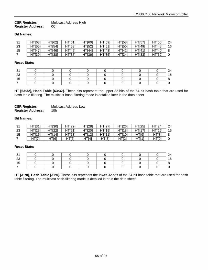
DS80C400 Network Microcontroller
55 of 97
CSR Register: Multicast Address High Register Address: 0Ch Bit Names: 31 HT[63] HT[62] HT[61] HT[60] HT[59] HT[58] HT[57] HT[56] 24 23 HT[55] HT[54] HT[53] HT[52] HT[51] HT[50] HT[49] HT[48] 16 15 HT[47] HT[46] HT[45] HT[44] HT[43] HT[42] HT[41] HT[40] 8 7 HT[39] HT[38] HT[37] HT[36] HT[35] HT[34] HT[33] HT[32] 0
Reset State: 31 0 0 0 0 0 0 0 0 24 23 0 0 0 0 0 0 0 0 16 15 0 0 0 0 0 0 0 0 8 7 0 0 0 0 0 0 0 0 0
HT [63:32], Hash Table [63:32]. These bits represent the upper 32 bits of the 64-bit hash table that are used for hash table filtering. The multicast hash-filtering mode is detailed later in the data sheet. CSR Register: Multicast Address Low Register Address: 10h Bit Names: 31 HT[31] HT[30] HT[29] HT[28] HT[27] HT[26] HT[25] HT[24] 24 23 HT[23] HT[22] HT[21] HT[20] HT[19] HT[18] HT[17] HT[16] 16 15 HT[15] HT[14] HT[13] HT[12] HT[11] HT[10] HT[9] HT[8] 8 7 HT[7] HT[6] HT[5] HT[4] HT[3] HT[2] HT[1] HT[0] 0
Reset State: 31 0 0 0 0 0 0 0 0 24 23 0 0 0 0 0 0 0 0 16 15 0 0 0 0 0 0 0 0 8 7 0 0 0 0 0 0 0 0 0
HT [31:0], Hash Table [31:0]. These bits represent the lower 32 bits of the 64-bit hash table that are used for hash table filtering. The multicast hash-filtering mode is detailed later in the data sheet.

DS80C400 Network Microcontroller
56 of 97
CSR Register: MII Address Register Address: 14h Bit Names: 31 — — — — — — — — 24 23 — — — — — — — — 16 15 PHYA [4:0] PHYR [4:2] 8 7 PHYR [1:0] — — — — W/ R BUSY 0
Reset State: 31 0 0 0 0 0 0 0 0 24 23 0 0 0 0 0 0 0 0 16 15 0 0 0 0 0 0 0 0 8 7 0 0 0 0 0 0 0 0 0
PHYA[4:0], PHY Address [4:0]. This 5-bit address specifies the PHY address for 2-wire MII serial-management bus communication. PHYR[4:0], PHY Register Select [4:0]. This 5-bit field specifies the PHY register to be accessed in 2-wire MII serial-management bus communication. W/R, Write/Read. This bit is used to indicate whether a write or read operation is to be requested of the addressed PHY/PHY register. 0 = read 1 = write BUSY, Busy. This status bit indicates when PHY communication is currently taking place on the MII serial-management bus. The application must wait until BUSY = 0 before modifying the MII address and MII data registers prior to each read/write operation. 0 = MII serial-management bus idle 1 = MII serial-management bus busy (write/read in progress) CSR Register: MII Data Register Address: 18h Bit Names: 31 — — — — — — — — 24 23 — — — — — — — — 16 15 PHYD [15:8] 8 7 PHYD [7:0] 0
Reset State: 31 0 0 0 0 0 0 0 0 24 23 0 0 0 0 0 0 0 0 16 15 0 0 0 0 0 0 0 0 8 7 0 0 0 0 0 0 0 0 0
PHYD[15:0], PHY Data [15:0]. These 16 bits contain the data read from the PHY register following a read operation, or the data to be written to the PHY register prior to a write operation.

DS80C400 Network Microcontroller
57 of 97
CSR Register: Flow Control Register Address: 1Ch Bit Names: 31 PAUSE [15:8] 24 23 PAUSE [7:0] 16 15 — — — — — — — — 8 7 — — — — — PCF FCE BUSY 0
Reset State: 31 0 0 0 0 0 0 0 0 24 23 0 0 0 0 0 0 0 0 16 15 0 0 0 0 0 0 0 0 8 7 0 0 0 0 0 0 0 0 0
PAUSE[15:0], Pause Time [15:0]. These bits are only valid in full-duplex mode. These 16 bits contain the value that is passed in the pause time field when a pause-control frame is generated. The format for the pause-control frame is shown in Figure 3. PCF, Pass Pause-Control Frame. This bit is valid for full-duplex mode only. This bit instructs the MAC whether or not to set the packet filter bit for pause-control frames. 0 = MAC decodes (if FCE = 1) but does not set the receive status word packet-filter bit (default) 1 = MAC decodes (if FCE = 1) and sets the packet-filter bit = 1 for pause-control frames FCE, Flow Control Enable 0 = MAC flow control is disabled (default) 1 = MAC flow control enabled; pause-control frame for full-duplex, back-pressure for half-duplex BUSY, Flow Control Busy. The BUSY bit is only valid in full-duplex mode. The BUSY bit should read logic 0 before initiating a pause-control frame. The BUSY bit should be set to logic 1 to initiate a pause-control frame. Upon successful transmission of a pause-control frame, the BUSY bit returns to logic 0. 0 = no pause-control frame currently being transmitted (default) 1 = initiate a pause-control frame Figure 3. Pause-Control Frame
ETHERNET FRAME
PREAMBLE SFD 01 80 C2 00 00 01 SOURCE ADDRESS 88 08 00 01 PAUSE TIME (2) PAD (42) CRC-32
(7) (1) (6) (6) (2) (46) (4)

DS80C400 Network Microcontroller
58 of 97
CSR Register: VLAN1 Tag Register Address: 20h Bit Names: 31 — — — — — — — — 24 23 — — — — — — — — 16 15 VLAN1 [15:8] 8 7 VLAN1 [7:0] 0
Reset State: 31 0 0 0 0 0 0 0 0 24 23 0 0 0 0 0 0 0 0 16 15 1 1 1 1 1 1 1 1 8 7 1 1 1 1 1 1 1 1 0
VLAN1 [15:0], VLAN1 Tag Identifier [15:0]. These 16 bits contain the VLAN1 tag that is compared against the 13th and 14th bytes of the incoming frame to determine whether it is a VLAN1 frame. If a non-zero match occurs, the max frame length is extended from 1518 Bytes to 1522 Bytes. CSR Register: VLAN2 Tag Register Address: 24h Bit Names: 31 — — — — — — — — 24 23 — — — — — — — — 16 15 VLAN2 [15:8] 8 7 VLAN2 [7:0] 0
Reset State: 31 0 0 0 0 0 0 0 0 24 23 0 0 0 0 0 0 0 0 16 15 1 1 1 1 1 1 1 1 8 7 1 1 1 1 1 1 1 1 0
VLAN2 [15:0], VLAN2 Tag Identifier [15:0]. These 16 bits contain the VLAN2 tag that is compared against the 13th and 14th bytes of the incoming frame to determine whether it is a VLAN2 frame. If a non-zero match occurs, the max frame length is extended from 1518 Bytes to 1538 Bytes.

DS80C400 Network Microcontroller
59 of 97
CSR Register: Wake-Up Frame Filter Register Address: 28h Bit Names: 31 WUFD [31:24] 24 23 WUFD [23:16] 16 15 WUFD [15:8] 8 7 WUFD [7:0] 0
Reset State: 31 0 0 0 0 0 0 0 0 24 23 0 0 0 0 0 0 0 0 16 15 0 0 0 0 0 0 0 0 8 7 0 0 0 0 0 0 0 0 0
WUFD [31:0], Wake-Up Frame Filter Data [31:0]. These 32 bits are used to access the four available network wake-up frame filters. Eight accesses to the wake-up frame filter register are needed to read or write all four wake-up frame filters. CSR Register: Wake-Up Events Control and Status Register Address: 2Ch Bit Names: 31 — — — — — — — — 24 23 — — — — — — — — 16 15 — — — — — — GU — 8 7 — WUFF MPF — — WUFE MPE — 0
Reset State: 31 0 0 0 0 0 0 0 0 24 23 0 0 0 0 0 0 0 0 16 15 0 0 0 0 0 0 0 0 8 7 0 0* 0* 0 0 0 0 0 0
*Power-on reset only. Unaffected by other reset sources. GU, Global Unicast 0 = frames must pass the destination address filter as well as the wake-up frame filter criteria in order to generate a wake-up event (default) 1 = frames must pass only the wake-up frame filter criteria to generate a wake-up event WUFF, Wake-Up Frame Received Flag. This bit is set to logic 1 to indicate when a wake-up event was generated due to the reception of a network wake-up frame. Application software must clear this flag by writing a 1 to this bit. MPF, Magic Packet Received Flag. This bit is set to logic 1 to indicate when a wake-up event was generated due to the reception of a Magic Packet. Application software must clear this flag by writing a 1 to this bit. WUFE, Wake-Up Frame Enable. Setting this bit to logic 1 invokes sleep mode and allows the reception of network wake-up frame to generate a wake-up event. MPE, Magic Packet Enable. Setting this bit to logic 1 invokes sleep mode and allows the reception of a Magic Packet to generate a wake-up event.
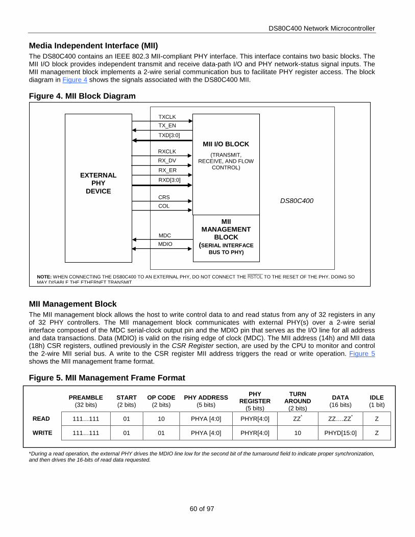
DS80C400 Network Microcontroller
60 of 97
Media Independent Interface (MII) The DS80C400 contains an IEEE 802.3 MII-compliant PHY interface. This interface contains two basic blocks. The MII I/O block provides independent transmit and receive data-path I/O and PHY network-status signal inputs. The MII management block implements a 2-wire serial communication bus to facilitate PHY register access. The block diagram in Figure 4 shows the signals associated with the DS80C400 MII. Figure 4. MII Block Diagram MII Management Block The MII management block allows the host to write control data to and read status from any of 32 registers in any of 32 PHY controllers. The MII management block communicates with external PHY(s) over a 2-wire serial interface composed of the MDC serial-clock output pin and the MDIO pin that serves as the I/O line for all address and data transactions. Data (MDIO) is valid on the rising edge of clock (MDC). The MII address (14h) and MII data (18h) CSR registers, outlined previously in the CSR Register section, are used by the CPU to monitor and control the 2-wire MII serial bus. A write to the CSR register MII address triggers the read or write operation. Figure 5 shows the MII management frame format. Figure 5. MII Management Frame Format
PREAMBLE (32 bits)
START (2 bits)
OP CODE (2 bits)
PHY ADDRESS (5 bits)
PHY REGISTER
(5 bits)
TURN AROUND
(2 bits)
DATA (16 bits)
IDLE (1 bit)
READ 111…111 01 10 PHYA [4:0] PHYR[4:0] ZZ* ZZ….ZZ* Z
WRITE 111…111 01 01 PHYA [4:0] PHYR[4:0] 10 PHYD[15:0] Z
*During a read operation, the external PHY drives the MDIO line low for the second bit of the turnaround field to indicate proper synchronization, and then drives the 16-bits of read data requested.
MDC
MII MANAGEMENT
BLOCK (SERIAL INTERFACE
BUS TO PHY)
MDIO
MII I/O BLOCK
(TRANSMIT, RECEIVE, AND FLOW
CONTROL)
EXTERNAL PHY
DEVICE
TX_EN
TXD[3:0]
RXCLK RX_DV
RX_ER
RXD[3:0]
CRS COL
TXCLK
DS80C400
NOTE: WHEN CONNECTING THE DS80C400 TO AN EXTERNAL PHY, DO NOT CONNECT THE RSTOL TO THE RESET OF THE PHY. DOING SO MAY DISABLE THE ETHERNET TRANSMIT.

DS80C400 Network Microcontroller
61 of 97
MII I/O Block The MII I/O block supports all of the transmit and receive data transactions between the DS80C400 MAC and the external PHY device as well as monitoring network status signals provided by the PHY. The transmit interface is composed of TXCLK, TX_EN, and TXD[3:0]. The TXCLK input is the transmit clock provided by the PHY. For 10Mbps operation, the transmit clock (TXCLK) should be run at 2.5MHz. For 100Mbps, TXCLK should be run at 25MHz. The TXD[3:0] outputs provide the 4-bit (nibble) data bus for transmitting frame data to the external PHY. Each transmission begins when the TX_EN output is driven active high, indicating to the PHY that valid data is present on the TXD[3:0] bus. The receive interface is composed of RXCLK, RX_DV, RX_ER, and RXD[3:0]. The RXCLK input is the receive clock provided by the external PHY. This clock (RXCLK) should be run at 2.5MHz for 10Mbps operation and at 25MHz for 100Mbps operation. The RXD[3:0] inputs serve as the 4-bit (nibble) data bus for receiving frame data from the external PHY. The reception begins when the external PHY drives the RX_DV input high, signaling that valid data is present on the RXD[3:0] bus. During reception of a frame (RX_DV = 1), the RX_ER input indicates whether the external PHY has detected an error in the current frame. The RX_ER input is ignored when not receiving a frame (RX_DV = 0). The MII also monitors two network status signals that are provided by the external PHY. The CRS (carrier sense) input is used to assess when the physical media is idle. The COL (collision detect) input is required for half-duplex operation to signal when a collision has occurred on the physical media. Ethernet Frames The basic purpose of the MII I/O block is to deliver and receive Ethernet frames to and from an external PHY, which controls the physical carrier. The format of the IEEE 802.3 Ethernet frame is shown in Figure 6. The preamble (7 Bytes) and start-of-frame delimiter (1 Byte) precede the Ethernet frame as a means of synchronizing to the start of the frame. The first two fields of the Ethernet frame are the destination address and the source address, each made up of 6 octets (bytes). The destination address field is the field examined by the address check block to determine whether the applied address filter criteria is met or not. The two bytes following the source address contain the Length or Type of frame. For Ethernet II (DIX) frames, these two bytes contain the Type field and the protocol for that specific frame type is embedded in the Data field. For frames where Length is specified in these two bytes, a header would typically follow in the Data field to convey type/protocol information for the frame (i.e., 802.2 or SNAP). Since the maximum Data field length for an Ethernet frame is 1500 Bytes, and all assigned frame types are greater than this value (1500d = 05DCh), one can easily distinguish whether the field holds Type or Length, allowing both kinds of frames to co-exist on the network. A special case occurs when the VLAN tag protocol ID (= 8100h) is encountered where the Length or Type is normally expected. The frame is then considered to be VLAN tagged. The VLAN frame format is described later. Figure 6. IEEE 802.3 Ethernet Frame
ETHERNET FRAME
PREAMBLE SFD DESTINATION ADDRESS SOURCE ADDRESS TYPE/LENGTH DATA CRC-32
(7) (1) (6) (6) (2) (46-1500) (4)

DS80C400 Network Microcontroller
62 of 97
Address Check Block The address check block of the Ethernet controller monitors the destination address of all incoming packets and determines whether the address passes or fails the filter criteria configured by CPU. The outcome of this address filter test, along with bits signaling whether the frame is a broadcast or multicast frame, is reported by the BCU in a packet’s receive status word. All incoming frames can be classified as one of three types: unicast, multicast, or broadcast (a special type of multicast). A unicast frame contains a 0 in the first received bit of the destination address and is intended for a single node on the network. A multicast frame contains a 1 in the first received bit of the destination address and is intended for multiple devices on the network. A broadcast frame is a multicast frame containing all 1’s in the destination address field and is intended for all network devices. Unless specifically disabled through the disable broadcast frame (DBF) bit in the CSR MAC control register (00h), broadcast frames are always received by the DS80C400 MAC. The address filter criteria is established using five bits found in the CSR MAC control register (00h). Three basic filter possibilities exist: perfect, inverse, and hash. Perfect filtering requires that the destination address perfectly match the MAC physical address that has been assigned in CSR registers MAC address high (04h) and MAC address low (08h). Inverse filtering requires that the destination address be anything other than the assigned MAC physical address. Perfect and inverse filtering are only applied to unicast frames. Hash filtering uses a user-defined hash table contained in CSR registers multicast address high (0Ch) and multicast address low (10h) to detect a successful address match. Figure 7 shows the five bits controlling the destination address filter. Table 15 gives the valid bit combinations and resultant filter modes. Note that some of the address filter mode control bits can instruct the address check block to automatically pass or fail certain types of frames. Figure 7. Address Filter Mode Control Bits CSR Register MAC Control (00h) 31 0
HP (MAC Control.13) Hash/Perfect Filtering Mode HO (MAC Control.15) Hash-Only Filtering Mode IF (MAC Control.17) Inverse Filtering PR (MAC Control.18) Promiscuous Mode PM (MAC Control.19) Pass All Multicast
Table 15. Address Filter Modes
FILTER MODE CONTROL BITS DESTINATION ADDRESS FILTER CRITERIA PM PR IF HO HP UNICAST MULTICAST 0 0 0 0 0 PERFECT FAIL 0 0 1 0 0 INVERSE FAIL 0 0 0 0 1 PERFECT HASH 1 0 0 0 x PERFECT PASS 0 0 0 1 1 HASH HASH 1 0 0 1 1 HASH PASS x 1 0 x x PASS (reset default state = 01000b)

DS80C400 Network Microcontroller
63 of 97
Multicast Hash Filter Hash filtering of destination addresses requires that a hash table be established. The hash table must be programmed into the CSR multicast address low and multicast address high registers. When hash filtering has been selected, the 6 bytes of the destination address are passed through the internal CRC-32 logic. The most significant 6 bits of the resultant CRC-32 are used to index into the hash table. From those 6 bits, the most significant bit determines whether multicast address high or low is used, while the lower 5 bits provide the bit index into the selected CSR register. If the multicast address high or low register bit indexed by the upper 6 bits of the CRC-32 is programmed to 1, then the destination address passes. Figure 8 shows the hash filtering process. Figure 8. Hash Table Index Generation VLAN Support The DS80C400 offers VLAN support through recognition of frames that are tagged as such. Each VLAN tag provides tag control information (TCI) containing a tag protocol ID (TPID) and VLAN ID. The incoming TPID occupy the 13th and 14th byte positions, those that would normally contain either the length or type field for the frame. The TPID is compared against the VLAN1 (20h) and VLAN2 (24h) CSR registers.
If a non-zero match occurs between the TPID and VLAN1 register setting, the frame is recognized as having a VLAN1 tag. For VLAN1 tagged frames, the TPID is followed by 2 Bytes containing the VLAN ID; therefore, the MAC extends the maximum legal frame length by a total of 4 Bytes (TPID = 2 Bytes, VLAN ID = 2 Bytes).
If a non-zero match occurs between the TPID and VLAN2 register setting, the frame is recognized as having a VLAN2 tag. For VLAN2 tagged frames, the TPID is followed by 18 Bytes containing the VLAN ID; therefore, the MAC extends the maximum legal frame length by a total of 20 Bytes (TPID = 2 Bytes, VLAN ID = 18 Bytes). Figure 9. VLAN Tagged Frame
ETHERNET FRAME
CRC-32 OF DESTINATION ADDRESS BYTES
PREAMBLE SFD DESTINATION ADDRESS SOURCE ADDRESS TYPE/LENGTH DATA CRC-32
CRC-32 GENERATOR
POLYNOMIAL . . . . . .
BIT INDEX 00000b: bit 0
00001b: bit 1 .
. 11110b: bit 30
11111b: bit 31
MULTICAST REGISTER SELECT 0: Multicast Address Low 1: Multicast Address High
TCI
ETHERNET FRAME PREAMBLE SFD DESTINATION ADDRESS SOURCE ADDRESS TYPE/LENGTH DATA CRC-32
(7) (1) (6) (6) (2) (46-1500) (4)
TPID VLAN ID
(2) (2: VLAN1) (18: VLAN2)
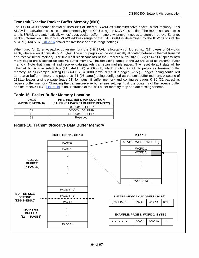
DS80C400 Network Microcontroller
64 of 97
Transmit/Receive Packet Buffer Memory (8kB) The DS80C400 Ethernet controller uses 8kB of internal SRAM as transmit/receive packet buffer memory. This SRAM is read/write accessible as data memory by the CPU using the MOVX instruction. The BCU also has access to this SRAM, and automatically writes/reads packet buffer memory whenever it needs to store or retrieve Ethernet packet information. The logical MOVX address range of the 8kB SRAM is determined by the IDM1:0 bits of the MCON (C6h) SFR. Table 16 shows the available address range settings. When used for Ethernet packet buffer memory, the 8kB SRAM is logically configured into (32) pages of 64 words each, where a word consists of 4 Bytes. These 32 pages can be dynamically allocated between Ethernet transmit and receive buffer memory. The five least significant bits of the Ethernet buffer size (EBS; E5h) SFR specify how many pages are allocated for receive buffer memory. The remaining pages of the 32 are used as transmit buffer memory. Note that transmit and receive data packets can span multiple pages. The reset default state of the Ethernet buffer size select bits (EBS.4–EBS.0) is 00000b, which configures all 32 pages as transmit buffer memory. As an example, setting EBS.4–EBS.0 = 10000b would result in pages 0–15 (16 pages) being configured as receive buffer memory and pages 16–31 (16 pages) being configured as transmit buffer memory. A setting of 11111b leaves a single page (page 31) for transmit buffer memory and configures pages 0–30 (31 pages) as receive buffer memory. Changing the transmit/receive buffer-size settings flush the contents of the receive buffer and the receive FIFO. Figure 10 is an illustration of the 8kB buffer memory map and addressing scheme. Table 16. Packet Buffer Memory Location
IDM1:0 (MCON.7, MCON.6)
INTERNAL 8kB SRAM LOCATION (ETHERNET PACKET BUFFER MEMORY)
00 00E000h–00FFFFh 01 000000h–001FFFh 10 FFE000h–FFFFFFh 11 Reserved
Figure 10. Transmit/Receive Data Buffer Memory
EXAMPLE: PAGE 1, WORD 2, BYTE 3
WORD 2
WORD 63
.
.
.
.
STATUS WORD (WORD 0)
WORD 1
.
.
.
.
.
.
.
.
.
PAGE 31
PAGE (n - 2)
PAGE (n - 1)
PAGE n
PAGE 0
PAGE 1
RECEIVE BUFFER
(n PAGES)
TRANSMIT BUFFER
(32 - n PAGES)
BUFFER SIZE SETTING
(EBS.4–EBS.0) (Per IDM1:0) PAGE WORD BYTE
8kB INTERNAL SRAM PAGE 1
xxxxxxxx xxx 00001 000010 11
BUFFER MEMORY ADDRESS (24-Bit)

DS80C400 Network Microcontroller
65 of 97
Transmit/Receive Status Words For each attempt made by the MAC to receive or transmit packet data, the BCU writes a 32-bit transmit or receive status word back to the first word of the starting page for the packet. This word provides status information needed by the CPU to determine when and what action should be taken. Transmit Status Word Bit Names: 31 RETRY — — — — — — — 24 23 — — — — — — — — 16 15 — HBF COL_CNT [3:0] OLTCOL DFR 8 7 NODAT XCOL LTCOL XDFR LSCRS NOCRS JABTO ABORT 0
RETRY, Packet Retry. This bit indicates that the current transmit packet has to be retried because of a collision on the bus. The application has to restart the transmission of the frame when this bit is set to 1. When this bit is reset, it indicates that the transmission of the current frame is completed. The success or failure to transmit a frame is indicated by the framed aborted (ABORT) bit. HBF, Heart-Beat Fail. This bit is only meaningful for ENDEC mode. This bit is not valid if the NODAT or XFDR bit is set. 0 = heart-beat collision check successful 1 = heart-beat collision check failed COL_CNT [3:0], Collision Count. These four bits indicate the number of collisions that occurred before the frame was transmitted. Collision count is valid only in half-duplex mode and it is not valid when the excessive collisions (XCOL) bit is set. OLTCOL, Late Collision Observed. This bit is only valid in half-duplex mode and is always set if the late collision abort (LTCOL) bit is set in the status word. 0 = no late collisions observed 1 = late collision (collision after the first time slot) observed. DFR, Deferred. This bit is only valid in half-duplex mode. 0 = no deferral required for the frame transmission attempt 1 = MAC had to defer while waiting to transmit because the carrier was not idle NODAT, Underrun 0 = transmit frame was not aborted due to data underrun 1 = transmit frame aborted because the MAC did not have sufficient data to complete the current frame transmission XCOL, Excessive Collisions. This bit is only valid in half-duplex mode. 0 = transmit frame was not aborted due to excessive collisions 1 = transmit frame aborted because of excessive collisions (16 transmit attempts unless DRTY = 1) LTCOL, Late Collision. This bit is only valid in half-duplex mode. 0 = transmit frame was not aborted due to a late collision 1 = transmit frame aborted due to collision occurring after the collision window of 64 Bytes. This bit is not valid if the NODAT bit is set. XDFR, Excessive Deferral. This bit is only valid in half-duplex mode when the MAC control register bit DFR is set. 0 = transmit frame was not aborted due to excessive deferral 1 = transmit frame aborted due to deferral of over 24,288 bit times LSCRS, Loss of Carrier. This bit is only valid in half-duplex mode. 0 = transmit frame was not aborted due to loss of carrier 1 = transmit frame aborted due to loss of carrier (CRS = 0 during the frame transmission)
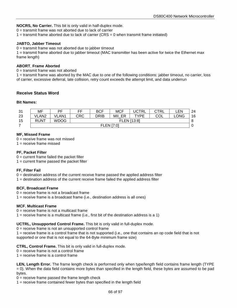
DS80C400 Network Microcontroller
66 of 97
NOCRS, No Carrier. This bit is only valid in half-duplex mode. 0 = transmit frame was not aborted due to lack of carrier 1 = transmit frame aborted due to lack of carrier (CRS = 0 when transmit frame initiated) JABTO, Jabber Timeout 0 = transmit frame was not aborted due to jabber timeout 1 = transmit frame aborted due to jabber timeout (MAC transmitter has been active for twice the Ethernet max frame length) ABORT, Frame Aborted 0 = transmit frame was not aborted 1 = transmit frame was aborted by the MAC due to one of the following conditions: jabber timeout, no carrier, loss of carrier, excessive deferral, late collision, retry count exceeds the attempt limit, and data underrun Receive Status Word Bit Names: 31 MF PF FF BCF MCF UCTRL CTRL LEN 24 23 VLAN2 VLAN1 CRC DRIB MII_ER TYPE COL LONG 16 15 RUNT WDOG FLEN [13:8] 8 7 FLEN [7:0] 0
MF, Missed Frame 0 = receive frame was not missed 1 = receive frame missed PF, Packet Filter 0 = current frame failed the packet filter 1 = current frame passed the packet filter FF, Filter Fail 0 = destination address of the current receive frame passed the applied address filter 1 = destination address of the current receive frame failed the applied address filter BCF, Broadcast Frame 0 = receive frame is not a broadcast frame 1 = receive frame is a broadcast frame (i.e., destination address is all ones) MCF, Multicast Frame 0 = receive frame is not a multicast frame 1 = receive frame is a multicast frame (i.e., first bit of the destination address is a 1) UCTRL, Unsupported Control Frame. This bit is only valid in full-duplex mode. 0 = receive frame is not an unsupported control frame 1 = receive frame is a control frame that is not supported (i.e., one that contains an op code field that is not supported or one that is not equal to the 64-Byte minimum frame size) CTRL, Control Frame. This bit is only valid in full-duplex mode. 0 = receive frame is not a control frame 1 = receive frame is a control frame LEN, Length Error. The frame length check is performed only when type/length field contains frame length (TYPE = 0). When the data field contains more bytes than specified in the length field, these bytes are assumed to be pad bytes. 0 = receive frame passed the frame length check 1 = receive frame contained fewer bytes than specified in the length field

DS80C400 Network Microcontroller
67 of 97
VLAN2, Two_Level VLAN Frame 0 = receive frame did not contain a VLAN tag that matched the VLAN2 register 1 = receive frame 13th and 14th bytes matched the two-level VLAN tag register (VLAN2) VLAN1, One_Level VLAN Frame 0 = receive frame did not contain a VLAN tag that matched the VLAN1 register 1 = receive frame 13th and 14th bytes matched the one-level VLAN tag register (VLAN1) CRC, CRC Error. This bit is also set to 1 if the RX_ER pin is asserted by the PHY during a reception, even if the CRC-32 for the frame is correct. 0 = CRC-32 error was not detected for the receive frame 1 = CRC-32 error was detected for the receive frame DRIB, Dribbling Bit. This bit is not valid if the COL or RUNT bits are set to 1. If DRIB = 1 and CRC = 0, then the packet is valid. 0 = receive frame did not contain any dribbling bits 1 = receive frame contained dribbling bits (a noninteger multiple of 8 bits) MII_ER, MII Error 0 = PHY did not assert the RX_ER signal during reception of the frame 1 = PHY asserted the RX_ER signal (indicating an error was detected) during the receive frame TYPE, Frame Type. This bit is not valid for runt frames less than 14 Bytes. 0 = length specified in the length/type field (i.e., value equal or less than 1500) 1 = type specified in the length/type field (i.e., value greater than 1500) COL, Collision Seen 0 = receive frame did not incur any collisions 1 = receive frame is damaged by a late collision (one that occurred after the first 64 bytes) LONG, Frame Too Long. This bit only serves as a status indicator and does not cause frame truncation. 0 = receive frame did not exceed the maximum frame length check 1 = receive frame exceeded the maximum frame length (1518 Bytes, unless VLAN tagged) RUNT, Runt Frame 0 = receive frame is not a runt frame (<64 Bytes) 1 = receive frame does not meet the minimum required frame size (64 Bytes = 1 time slot) due to a collision or premature frame termination WDOG, Watchdog Timeout. The FLEN[13:0] field is not valid when this bit is set. 0 = MAC watchdog timer did not timeout during the receive frame 1 = MAC watchdog timer timed out during the receive frame. The watchdog timer is programmed to twice the maximum frame length (3036 bit times). FLEN [13:0], Frame Length [13:0]. This field indicates the receive frame length in bytes, including zero padding pad (if applicable) and the CRC-32 field, unless automatic pad stripping has been enabled (ASTP = 1). When ASTP = 1, the frame length includes only the data field.

DS80C400 Network Microcontroller
68 of 97
Ethernet Interrupts The DS80C400 Ethernet controller supports two interrupt sources: Ethernet power-mode interrupt and the Ethernet activity interrupt. Each interrupt source has its own enable, priority, and flag bits. The locations of these bits are documented in the interrupt vector table later in the data sheet (Table 28). Both interrupt sources are globally enabled or disabled by the EA bit in the IE SFR and both require that the interrupt flags be manually cleared by application software. The Ethernet power-mode interrupt source, if enabled, can be generated on the reception of a Magic Packet or network wake-up frame while the Ethernet controller is in sleep mode. The Ethernet activity interrupt can be triggered when the BCU reports the status of either a transmit or receive packet. Power Management Block The DS80C400 Ethernet controller contains a power management block that allows it to be put into a sleep mode by the CPU, thus conserving power when not actively handling Ethernet traffic. Sleep mode can be invoked in two different ways. The CPU can issue the ‘Enable Sleep Mode’ command to the BCU by simply writing the BCUC SFR = 1100b. Alternatively, the Ethernet controller is put into sleep mode when one or both of the possible wake-up frame sources are enabled. The enable bits for these two wake-up sources, network wake-up frame and Magic Packet frame, are located in the CSR wake-up frame control and status register (2Ch). If the network wake-up frame is intended as a wake-up source, the CSR wake-up frame filter register (28h) should be programmed accordingly prior to invoking sleep mode. If sleep mode is invoked using the ‘Enable Sleep Mode’ command, the Ethernet controller can be awakened by the ‘Disable Sleep Mode’ command or by either of the two special wake-up frames. If sleep mode is invoked by enabling one or both wake-up frame sources, only the enabled wake-up frame(s) can remove the condition. To resume normal Ethernet operation, all enable bits and flag bits (including EPMF of the BCUC SFR) should be cleared and if the ‘Enable Sleep Mode’ command was used to invoke sleep mode, then the ‘Disable Sleep Mode’ command must be issued. Magic Packet and Network Wake-Up Frame The power management block recognizes two types of frames, Magic Packet and network wake-up frame, as capable of awakening the Ethernet controller from sleep mode. In order for either type of frame to serve as a wake-up source, it must be programmed to do so. A Magic Packet is an error-free frame that passes the current destination address filter and that, anywhere after the source address, contains a data sequence of FFFF_FFFF_FFFFh immediately followed by 16 iterations of the MAC physical address. When a Magic Packet is detected by the power management block, the Magic Packet-received bit (bit 5 of CSR wake-up events control and status register) is set, and an interrupt request to the CPU is generated if enabled (EPMI = 1). A network wake-up frame is one that passes any of the four user-defined frame filters that have been programmed into the CSR wake-up frame filter register (28h) and passes the destination address filter (if GU = 0). Each filter is composed of a command, an offset, a byte mask, and a CRC. The command nibble contains a bit (MSB of command) to select whether unicast (= 0) or multicast (= 1) frames are to be checked and a bit (LSB of command) used to disable (= 0) or enable (= 1) that individual frame filter. The offset defines the location of the first byte to be checked in each potential wake-up frame. Since the destination address is checked by the address check block, the offset should always be greater than 12. The byte mask is used to define which of the 31 bytes, beginning at the offset, are to be used for the CRC calculation. Bit 31 of the byte mask is always 0, but for each bit j of the byte mask that is set to a logic 1, byte (offset + j) is included in the CRC-16 calculation. The CRC contains the CRC-16 of the pattern bytes needed to cause a wake-up event. When a network wake-up frame is recognized, the wake-up frame received bit (bit 6 of CSR wake-up events control and status register) becomes set and an interrupt request to the CPU is generated if enabled (EPMI = 1). The wake-up frame-filter register structure is shown in Figure 11.

DS80C400 Network Microcontroller
69 of 97
Figure 11. Wake-Up Frame-Filter Structure 31 0
FILTER 0 BYTE MASK FILTER 1 BYTE MASK FILTER 2 BYTE MASK FILTER 3 BYTE MASK
RESERVED FILTER 3 COMMAND RESERVED FILTER 2
COMMAND RESERVED FILTER 1 COMMAND RESERVED FILTER 0
COMMAND FILTER 3 OFFSET FILTER 2 OFFSET FILTER 1 OFFSET FILTER 0 OFFSET
FILTER 1 CRC-16 FILTER 0 CRC-16 FILTER 3 CRC-16 FILTER 2 CRC-16
Embedded ROM Firmware The DS80C400 incorporates an embedded ROM specifically designed for hosting the MxTNI™ runtime environment and the MxTNI C libraries. The ROM firmware implements three major components: a full TCP/IPv4/6 stack with industry-standard Berkeley socket interface, a preemptive task scheduler, and NetBoot functionality. The NetBoot component uses the TCP/IP stack, socket layer, and task scheduler to provide automatic network boot capability. NetBoot allows an application to be downloaded from the network and executed by the microcontroller.
To use the ROM firmware, the system is required to have the following hardware components: • 64kB SRAM external memory, mapped (Note 1) at address locations 000000h–00FFFFh • Memory (SRAM or flash) to store user-application code • DS2502(-E48) 1-Wire chip (to hold physical MAC address) (Note 2) • External crystal or oscillator (Note 3) Note 1: Merged program/data memory configuration is required. Note 2: Java applications and NetBoot require a DS2502(-E48). Applications written in C can program the MAC address. Note 3: NetBoot functionality requires the external clock frequency to be at least 7MHz. The clock doubleris not turned on until after NetBoot, thus 100Mbps NetBoot is not possible unless the external clock source is at least 25MHz. When not in NetBoot, the system clock (external clock source after internal multiplication or division) must be a minimum of 25MHz for use of the Ethernet 100Mbps mode. Selecting ROM Code Execution The DS80C400, following each reset, begins execution of program code at address location 000000h. Since the DS80C400 contains internal ROM and supports external program code, the user must select which of these two program memory spaces should be accessed for initial program fetching. There are two mechanisms that control selection of the internal DS80C400 ROM code. These two controls are the EA pin and the bypass ROM (BROM) SFR bit. No matter the state of the BROM bit, if the EA pin is held at a logic low level, the ROM code is not entered and is not accessible to the user code. If the EA pin is at a logic high level, the BROM bit is then examined to determine whether the internal ROM firmware should be executed or bypassed. If BROM = 0, the ROM code is executed. Otherwise (BROM = 1), the ROM is bypassed and execution is transferred to external user code at address 000000h. The BROM bit defaults to 0 on a power-on reset, but is unaffected by other reset sources. This code selection process can be seen in Figure 12. DS80C400 ROM Code Execution Flow Once the internal DS80C400 ROM code has been selected (EA = 1, BROM = 0), it must first execute some basic configuration code to provide functionality to subsequent ROM operations. Next, the ROM code reads the state of port pin P1.7. The ROM associates the logic state of P1.7 with the user desire to invoke the serial loader function. If the serial loader pin (P1.7) is a logic 1, the ROM monitors for activity on serial port 0 and tries to respond to the external host with its own serial banner. Once serial communication has been established at a supported baud rate, signified by correct reception of the DS80C400 loader banner and prompt, the user can issue commands. The serial loader commands are described later in the data sheet. If the serial loader pin is pulled to a logic 0, the ROM reads the state of port pin P5.3. Much like the association made between P1.7 and invocation of the serial loader, the ROM links the logic state of P5.3 with the user desire to begin the NetBoot process. If the NetBoot pin (P5.3) is asserted (logic 0), the ROM initiates the NetBoot process. If the NetBoot pin is not asserted (logic 1), the ROM executes the find-user-code routine to identify executable user code. Figure 12 illustrates the ROM decisions described above.
MxTNI is a trademark of Maxim Integrated Products, Inc.

DS80C400 Network Microcontroller
70 of 97
Figure 12. ROM Code Boot Sequence

DS80C400 Network Microcontroller
71 of 97
DS80C400 ROM Initialization Code The 80C400 firmware automatically executes Initialization Code (ROM_Init) to generate the memory map as shown in Figure 13 and configure the DS80C400 hardware as follows: Enables 24-bit contiguous address mode (ACON.1:0 = 11b) Logically relocates ROM to addresses FF0000h–FF7FFFh (ACON.5 =1) Enables CE0–3, 2MB/chip enable (P4CNT = 2Fh) Enables PCE0–3 (P5CNT = 07h) Enables CE4–7, 1M/peripheral chip enable (P6CNT = 27h) Merged program/data CE0–3, relocate internal XRAM (MCON = AFh) Enables extended 1kB stack option (ACON.2 = 1) Configure to maximum MOVX stretch value (CKCON.2:0 = 111b) Configure UARTs for Mode 1 serial operation Figure 13. Memory Map Following Execution of ROM_Init
00FFFFh
800000h -
A00000h -
C00000h -
E00000h -
FFFFFFh -
600000h -
400000h -
200000h -
000000h -
INTERNAL MEMORY program data
EXTERNAL MEMORY merged program/data space
CE7
CE6
CE5
CE4
CE3
CE2
CE1
CE0
DATA INACCESSIBLE
64kB SRAM REQUIRED
PROGRAM INACCESSIBLE
ROM CAN/BCU XRAM
FF0000h
FFDB00h
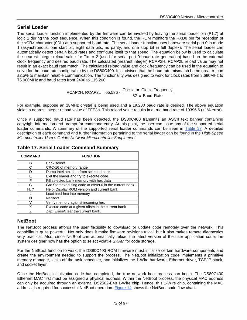
DS80C400 Network Microcontroller
72 of 97
Serial Loader The serial loader function implemented by the firmware can be invoked by leaving the serial loader pin (P1.7) at logic 1 during the boot sequence. When this condition is found, the ROM monitors the RXD0 pin for reception of the <CR> character (0Dh) at a supported baud rate. The serial loader function uses hardware serial port 0 in mode 1 (asynchronous, one start bit, eight data bits, no parity, and one stop bit in full duplex). The serial loader can automatically detect certain baud rates and configure itself to that speed. The equation below is used to calculate the nearest integer-reload value for Timer 2 (used for serial port 0 baud rate generation) based on the external clock frequency and desired baud rate. The calculated (nearest integer) RCAP2H, RCAP2L reload value may not result in an exact baud rate match. The calculated reload value and clock frequency can be used in the equation to solve for the baud rate configurable by the DS80C400. It is advised that the baud rate mismatch be no greater than ±2.5% to maintain reliable communication. The functionality was designed to work for clock rates from 3.680MHz to 75.000MHz and baud rates from 2400 to 115,200.
RCAP2H, RCAP2L = 65,536 - Rate Baud x 32Frequency Clock Oscillator
For example, suppose an 18MHz crystal is being used and a 19,200 baud rate is desired. The above equation yields a nearest integer reload value of FFE3h. This reload value results in a true baud rate of 19396.6 (+1% error). Once a supported baud rate has been detected, the DS80C400 transmits an ASCII text banner containing copyright information and prompt for command entry. At this point, the user can issue any of the supported serial loader commands. A summary of the supported serial loader commands can be seen in Table 17. A detailed description of each command and further information pertaining to the serial loader can be found in the High-Speed Microcontroller User’s Guide: Network Microcontroller Supplement. Table 17. Serial Loader Command Summary
COMMAND FUNCTION
B Bank select C CRC-16 of memory range D Dump Intel hex data from selected bank E Exit the loader and try to execute code F Fill selected bank memory with hex data G Go: Start executing code at offset 0 in the current bank
H, ? Help: Display ROM version and current bank L Load Intel hex into memory N NetBoot V Verify memory against incoming hex X Execute code at a given offset in the current bank Z Zap: Erase/clear the current bank.
NetBoot The NetBoot process affords the user flexibility to download or update code remotely over the network. This capability is quite powerful. Not only does it make firmware revisions trivial, but it also makes remote diagnostics very practical. Also, since NetBoot can automatically reload the latest version of the user application code, the system designer now has the option to select volatile SRAM for code storage. For the NetBoot function to work, the DS80C400 ROM firmware must initialize certain hardware components and create the environment needed to support the process. The NetBoot initialization code implements a primitive memory manager, kicks off the task scheduler, and initializes the 1-Wire hardware, Ethernet driver, TCP/IP stack, and socket layer. Once the NetBoot initialization code has completed, the true network boot process can begin. The DS80C400 Ethernet MAC first must be assigned a physical address. Within the NetBoot process, the physical MAC address can only be acquired through an external DS2502-E48 1-Wire chip. Hence, this 1-Wire chip, containing the MAC address, is required for successful NetBoot operation. Figure 14 shows the NetBoot code flow chart.

DS80C400 Network Microcontroller
73 of 97
Figure 14. NetBoot Code Flow Chart Next, the DS80C400 ROM searches the 1-Wire bus for an external device (separate from the device containing the MAC address) that contains an IP address and TFTP server IP address. In order to correctly acquire the IP and TFTP server addresses from an external 1-Wire device, the data read from the device must conform to a specific format. This format is shown in Figure 15. Figure 15. 1-Wire IP and TFTP Server IP Address Format If the IP and TFTP server addresses cannot be acquired from a 1-Wire device, the NetBoot process uses DHCP to get this information. The DS80C400 broadcasts its MAC address in a DHCP Discover packet. A DHCP server, if available, should then respond with an IP address offering. The DS80C400 subsequently requests the IP address, to which the DHCP server must acknowledge. In the DHCP acknowledge packet, the TFTP server IP address is then read from the “next server IP” field. Because some DHCP servers do not allow configuration of the “next server IP” field, the DS80C400 recognizes the site-specific option 150 (also used on Cisco IP phones to get TFTP server IP addresses). When option 150 is present in the acknowledge packet, it will take precedence over the “next server IP” field.
IPv4 or IPv6 IPv4 IPv4 ‘TINI’
1Dh 54h,49h,4Eh,49h Address(4) Gateway(4) PrefixLength(1) TFTP Server Address(16) Checksum(2)
1’S COMPLEMENT OF CRC-16 (LSB
FIRST) 29 (LENGTH)
IPV4 (BYTE
CONVERTED TO SUBNET MASK)
NETBOOT INITIALIZATION CODE
ACQUIRE MAC ADDRESS FROM DS2502
1-WIRE DEVICE WITH IP
ADDRESS
FIND USER CODE
TFTP/FLASH WRITE
DHCP
GET IP ADDRESS FROM 1-WIRE DEVICE
NetBoot PROCESS
Y
N
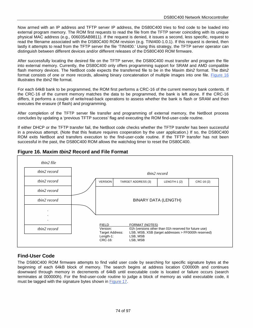
DS80C400 Network Microcontroller
74 of 97
Now armed with an IP address and TFTP server IP address, the DS80C400 tries to find code to be loaded into external program memory. The ROM first requests to read the file from the TFTP server coinciding with its unique physical MAC address (e.g., 006035AB9811). If the request is denied, it issues a second, less specific, request to read the filename associated with the DS80C400 ROM revision (e.g. TINI400-1.0.1). If this request is denied, then lastly it attempts to read from the TFTP server the file ‘TINI400.’ Using this strategy, the TFTP server operator can distinguish between different devices and/or different releases of the DS80C400 ROM firmware. After successfully locating the desired file on the TFTP server, the DS80C400 must transfer and program the file into external memory. Currently, the DS80C400 only offers programming support for SRAM and AMD compatible flash memory devices. The NetBoot code expects the transferred file to be in the Maxim tbin2 format. The tbin2 format consists of one or more records, allowing binary concatenation of multiple images into one file. Figure 16 illustrates the tbin2 file format. For each 64kB bank to be programmed, the ROM first performs a CRC-16 of the current memory bank contents. If the CRC-16 of the current memory matches the data to be programmed, the bank is left alone. If the CRC-16 differs, it performs a couple of write/read-back operations to assess whether the bank is flash or SRAM and then executes the erasure (if flash) and programming. After completion of the TFTP server file transfer and programming of external memory, the NetBoot process concludes by updating a ‘previous TFTP success’ flag and executing the ROM find-user-code routine. If either DHCP or the TFTP transfer fail, the NetBoot code checks whether the TFTP transfer has been successful in a previous attempt. (Note that this feature requires cooperation by the user application.) If so, the DS80C400 ROM exits NetBoot and transfers execution to the find-user-code routine. If the TFTP transfer has not been successful in the past, the DS80C400 ROM allows the watchdog timer to reset the DS80C400. Figure 16. Maxim tbin2 Record and File Format Find-User Code The DS80C400 ROM firmware attempts to find valid user code by searching for specific signature bytes at the beginning of each 64kB block of memory. The search begins at address location C00000h and continues downward through memory in decrements of 64kB until executable code is located or failure occurs (search terminates at 000000h). For the find-user-code routine to judge a block of memory as valid executable code, it must be tagged with the signature bytes shown in Figure 17.
VERSION TARGET ADDRESS (3) LENGTH-1 (2) CRC-16 (2)
BINARY DATA (LENGTH)
tbin2 record tbin2 record
tbin2 record
tbin2 record
tbin2 record . . .
tbin2 record
tbin2 file
FIELD FORMAT (NOTES) Version: 01h (versions other than 01h reserved for future use) Target Address: LSB, MSB, XSB (target addresses > FF0000h reserved) Length-1: LSB, MSB CRC-16: LSB, MSB

DS80C400 Network Microcontroller
75 of 97
Figure 17. User Code Signature (Required by Find-User Code)
Once a valid signature is found, the signature byte at offset 6, referred to in Figure 17 as the segment address, is examined to determine whether execution control should be transferred immediately or whether the search should continue. If the segment address byte equals 00h or matches the most significant address byte for the 64kB block being examined, execution is transferred to the user code. If the segment address byte does not match, that segment address byte is used to determine the next memory block examined for a valid signature. Exported ROM Functions The DS80C400 ROM firmware implements many functions that are made accessible to the user application code. For user application code to call a specific function, the location of that function must be known. The absolute address location of each DS80C400 ROM function must be read from an export table (also found in the ROM). To allow flexibility for future ROM firmware structural changes and improvements, the export table itself is not connected to a specific address range, but instead a 3-Byte pointer to the start of the export table is fixed at addresses FF0002h (XSB), FF0003h (MSB), and FF0004h (LSB). The first three bytes of the export table contain the quantity of function entries in the export table. In 3-Byte increments, following the first three bytes, the rest of the table contains absolute address locations for the exported ROM functions. Thus, once the export table location has been discovered, the index for a given function/structure (Table 18) can be used to find its absolute address (Function address = ExportTable[Index x 3]). Figure 18 illustrates the method for locating the export table and a specific ROM function. Table 18 shows the contents of the ROM export table. Brief descriptions of the functionality provided by the TCP/IP stack, socket layer, and task manager are included after the table, while the full details for these and other exported ROM functions are covered in the High-Speed Microcontroller User’s Guide: Network Microcontroller Supplement. Figure 18. Finding the Location of an Exported ROM Function
SJMP xx ‘TINI’
80h,xxh 54h,49h,4Eh,49h Segment Address(1) USER CODE
SIGNATURE BYTES
1
TINI400 ROM (LOGICALLY LOCATED FF0000h–
FFFFFFh WHEN MROM = 1)
ROM Export Table
FF0000h
ROM FUNCTION EXPORT TABLE
ROM Exported Function [3]
FFxxxxh
Export Table Address
FFFFFFh
.
.
.
Number of Functions Exported (n)
Function [index=1] Address
Function [2] Address
Function [3] Address
Function [n] Address
FFxxxxh
FFxxxxh +03h
FFxxxxh +06h
FFxxxxh +09h
FFxxxxh +(n x 3)h
2

DS80C400 Network Microcontroller
76 of 97
Table 18. ROM Export Table INDEX FUNCTION DESCRIPTION/GROUP
0 Num_Fn,0,0 Number of functions following in the table 1 crc16 Utility functions 2 mem_clear 3 mem_copy 4 mem_compare 5 add_dptr0 6 add_dptr1 7 sub_dptr0 8 sub_dptr1 9 getpseudorandom
10 rom_kernelmalloc Memory manager 11 rom_kernelfree 12 rom_malloc 13 rom_malloc_dirty 14 rom_free 15 rom_deref 16 rom_getfreeram 17 socket Socket functions 18 closesocket 19 sendto 20 recvfrom 21 connect 22 bind 23 listen 24 accept 25 recv 26 send 27 getsockopt 28 setsockopt 29 getsockname 30 getpeername 31 cleanup 32 avail 33 join 34 leave 35 ping 36 getnetworkparams 37 setnetworkparams 38 getipv6params 39 getethernetstatus 40 gettftpserver 41 settftpserver 42 eth_processinterrupt Ethernet interrupt handler 43 arp_generaterequest Generates ARP request 44 MAC_ID Pointer to MAC ID 45 dhcp_init DHCP functions 46 dhcp_setup 47 dhcp_startup 48 dhcp_run 49 dhcp_status 50 dhcp_stop 51 rom_dhcp_notify 52 tftp_init TFTP functions 53 tftp_first 54 tftp_next 55 TFTP_MSG 56 task_genesis Task scheduler functions 57 task_getcurrent 58 task_getpriority 59 task_setpriority 60 task_fork

DS80C400 Network Microcontroller
77 of 97
INDEX FUNCTION DESCRIPTION/GROUP 61 task_kill 62 task_suspend 63 task_sleep 64 task_signal 65 rom_task_switch_in 66 rom_task_switch_out 67 EnterCritSection Enter/Leave critical section 68 LeaveCritSection 69 rom_init Initialization functions 70 rom_copyivt 71 rom_redirect_init 72 mm_init 73 km_init 74 ow_init 75 network_init 76 eth_init 77 init_sockets 78 tick_init 79 WOS_Tick Timer interrupt handler 80 BLOB Start address of the memory area ignored by NetBoot 81 WOS_IOPoll Asynchronous TCP/IP maintenance functions 82 IP_ProcessReceiveQueues 83 IP_ProcessOutput 84 TCP_RetryTop 85 ETH_ProcessOutput 86 IGMP_GroupMaintenance 87 IP6_ProcessReceiveQueues 88 IP6_ProcessOutput 89 PARAMBUFFER Pointer to parameter buffer 90 RAM_TOP Address of pointer to end of RAM used by NetBoot 91 BOOT_MEMBEGIN 92 BOOT_MEMEND 93 OWM_First 1-Wire master functions 94 OWM_Next 95 OWM_Reset 96 OWM_Byte 97 OWM_Search 98 OWM_ROMID 99 Autobaud Serial port 0 baud rate detection
100 tftp_close

DS80C400 Network Microcontroller
78 of 97
TCP/IP Stack and Berkeley Sockets The ROM firmware implements TCP/IP Ethernet networking over an industry-standard/Berkeley socket interface. The stack supports TCP and UDP transport protocols, allowing a maximum of 24 client/server sockets for either IPv4 or IPv6. Table 19 lists the socket functions implemented and accessible in the ROM firmware. The full details of each socket function are contained in the High-Speed Microcontroller User’s Guide: Network Microcontroller Supplement.
Figure 19 illustrates the typical sequences for using TCP/UDP client/server sockets. The IPv4 implementation supports multicasting, ICMP echo request (“ping”), DHCP client, and TFTP client. It does not, however, allow IP packet fragmentation or reassembly, and it ignores the extended IP options field. The IPv6 implementation supports ICMP and the TFTP client protocols. Table 19. Socket Functions
FUNCTION DESCRIPTION socket Creates the specified TCP or UDP network socket closesocket Closes the specified socket sendto Sends a UDP datagram to the specified address recvfrom Receives a UDP datagram connect Connects a TCP socket to the specified address bind Binds a socket to the specified address, port listen Listens for connections on the specified socket accept Accepts a TCP connection on the specified socket recv Reads data from the specified TCP socket connection send Sends data to the specified TCP socket connection getsockopt Gets options for the specified socket setsockopt Sets options for the specified socket getsockname Gets current local address for the specified socket getpeername Gets current remote address for the specified TCP socket cleanup Closes all sockets associated with the specified task ID avail Returns the number of bytes available for reading on the specified TCP socket join Adds the specified UDP socket to a specified multicast group leave Removes the specified UDP socket from a specified multicast group ping Sends ICMP echo request to the specified address setnetworkparams Sets the IPv4 address and configuration parameters getnetworkparams Gets the IPv4 address and configuration parameters getipv6params Gets the IPv6 address getethernetstatus Gets the status of the Ethernet link gettftpserver Gets the IP address of the TFTP server settftpserver Sets the IP address of the TFTP server
Figure 19. Typical TCP/UDP Sockets
UDP UDP Unicast Multicast
TCP TCP Server Client
socket
bind, getsockopt, setsockopt (optional)
listen (max. 16)
accept connect
avail, send, recv
sendto, recvfrom
closesocket
join
leave

DS80C400 Network Microcontroller
79 of 97
Task Scheduler The DS80C400 ROM firmware implements a priority based preemptive task scheduler. Each task created is represented in a task ring by a corresponding task control block (TCB). The TCB holds critical information specific to the task, such as the ID, priority, event bit mask, wake-up time, and pointers to state information and next task. Using a timer, the scheduler is run approximately every 4ms (at 18.432MHz crystal frequency) unless deferred because another interrupt is in progress. The scheduler supports an unlimited number of tasks and allows addition, deletion, or modification on the fly. However, one should realize that increasing the number of tasks increases the time needed by the scheduler to search and prioritize the ring. The High-Speed Microcontroller User’s Guide: Network Microcontroller Supplement provides greater detail about the task scheduler and its functionality. Controller Area Network (CAN) Module The DS80C400 incorporates one CAN controller that is fully compliant with the CAN 2.0B specification. CAN is a highly robust, high-performance communication protocol for serial communications. Popular in a wide range of applications including medical, heating, ventilation, and industrial control, the CAN architecture allows for the construction of sophisticated networks with a minimum of external hardware.
The CAN controller supports the use of 11-bit standard or 29-bit extended acceptance identifiers for up to 15 messages, with the standard 8-Byte data field, in each message. Fourteen of the 15 message centers are programmable in either transmit or receive modes, with the 15th designated as an FIFO-buffered, receive-only message center to help prevent data overruns. All message centers have two separate 8-bit media masks and media arbitration fields for incoming message verification. This feature supports the use of higher-level protocols that use the first and/or second byte of data as a part of the acceptance layer for storing incoming messages. Each message center can also be programmed independently to test incoming data with or without the use of the global masks.
Global controls and status registers in the CAN unit allow the microcontroller to evaluate error messages, generate interrupts, locate and validate new data, establish the CAN bus timing, establish identification mask bits, and verify the source of individual messages. Each message center is individually equipped with the necessary status and control bits to establish direction, identification mode (standard or extended), data field size, data status, automatic remote frame request and acknowledgment, and perform masked or nonmasked identification-acceptance testing. Communicating with the CAN Module The microcontroller interface to the CAN modules is divided into two groups of registers. All the global CAN status and control bits as well as the individual message center control/status registers are located in the SFR map. The remaining registers associated with the message centers (data identification, identification/arbitration masks, format and data) are located in MOVX data space. The CMA bit (MCON.5) allows the message centers to be mapped to either 00DB00h–00DBFFh (CMA = 0) or FFDB00h–FFDBFFh (CMA = 1), reducing the possibility of a memory conflict with application software. The internal architecture of the DS80C400 requires that the device be in one of the two 24-bit addressing modes when the CMA bit is set to correctly access the CAN MOVX memory. A special lockout feature prevents the accidental software corruption of the control, status, and mask registers while a CAN operation is in progress. Each CAN controller uses a total of 15 message centers. Each message center is composed of four specific areas that include the following:
1) Four arbitration registers (C0MxAR0-3) that store either the 11-bit or 29-bit arbitration value. These registers are located in the MOVX memory map.
2) A format register (C0MxF) that informs the CAN controller as to the direction (transmit or receive), the number of data bytes in the message, the identification format (standard or extended), and the optional use of the identification mask or media mask during message evaluation. This register is located in the MOVX memory map.
3) Eight data bytes for storage of 0 to 8 Bytes of data (C0MxD0–7) are located in the MOVX memory map. 4) Message control registers (C0MxC) are located in the SFR memory for fast access.
Each of the message centers is identical with the exception of message center 15. Message center 15 has been designed as a receive-only center and is also buffered through the use of a two-message FIFO to help prevent message loss in a message-overrun situation. The receipt of a third message before either of the first two are read overwrites the second message, leaving the first message undisturbed.

DS80C400 Network Microcontroller
80 of 97
Modification of the CAN registers located in MOVX memory is protected through the SWINT bit. Consult the description of this bit in the High-Speed Microcontroller User’s Guide: Network Microcontroller Supplement for more information. The CAN module contains a block of control/status/mask registers, 14 functionally identical message centers, plus a 15th message center that is receive-only and incorporates a buffered FIFO. Table 20 describes the organization of the message centers located in MOVX space. Table 20. CAN Controller MOVX Memory Map CONTROL/STATUS/MASK REGISTERS
REGISTER 7 6 5 4 3 2 1 0 MOVX DATA ADDRESS*
C0MID0 MID07 MID06 MID05 MID04 MID03 MID02 MID01 MID00 xxDB00h C0MA0 M0AA7 M0AA6 M0AA5 M0AA4 M0AA3 M0AA2 M0AA1 M0AA0 xxDB01h C0MID1 MID17 MID16 MID15 MID14 MID13 MID12 MID11 MID10 xxDB02h C0MA1 M1AA7 M1AA6 M1AA5 M1AA4 M1AA3 M1AA2 M1AA1 M1AA0 xxDB03h C0BT0 SJW1 SJW0 BPR5 BPR4 BPR3 BPR2 BPR1 BPR0 xxDB04h C0BT1 SMP TSEG26 TSEG25 TSEG24 TSEG13 TSEG12 TSEG11 TSEG10 xxDB05h
C0SGM0 ID28 ID27 ID26 ID25 ID24 ID23 ID22 ID21 xxDB06h C0SGM1 ID20 ID19 ID18 0 0 0 0 0 xxDB07h C0EGM0 ID28 ID27 ID26 ID25 ID24 ID23 ID22 ID21 xxDB08h C0EGM1 ID20 ID19 ID18 ID17 ID16 ID15 ID14 ID13 xxDB09h C0EGM2 ID12 ID11 ID10 ID9 ID8 ID7 ID6 ID5 xxDB0Ah C0EGM3 ID4 ID3 ID2 ID1 ID0 0 0 0 xxDB0Bh C0M15M0 ID28 ID27 ID26 ID25 ID24 ID23 ID22 ID21 xxDB0Ch C0M15M1 ID20 ID19 ID18 ID17 ID16 ID15 ID14 ID13 xxDB0Dh C0M15M2 ID12 ID11 ID10 ID9 ID8 ID7 ID6 ID5 xxDB0Eh C0M15M3 ID4 ID3 ID2 ID1 ID0 0 0 0 xxDB0Fh
CAN 0 MESSAGE CENTER 1 RESERVED xxDB10h–11h
C0M1AR0 CAN 0 MESSAGE 1 ARBITRATION REGISTER 0 xxDB12h C0M1AR1 CAN 0 MESSAGE 1 ARBITRATION REGISTER 1 xxDB13h C0M1AR2 CAN 0 MESSAGE 1 ARBITRATION REGISTER 2 xxDB14h C0M1AR3 CAN 0 MESSAGE 1 ARBITRATION REGISTER 3 WTOE xxDB15h
C0M1F DTBYC3 DTBYC2 DTBYC1 DTBYC0 T/R EX/ST MEME MDME xxDB16h C0M1D0–7 CAN 0 MESSAGE 1 DATA BYTES 0 to 7 xxDB17h–1Eh
RESERVED xxDB1Fh CAN 0 MESSAGE CENTERS 2 to 14
MESSAGE CENTER 2 REGISTERS (similar to Message Center 1) xxDB20h–2Fh MESSAGE CENTER 3 REGISTERS (similar to Message Center 1) xxDB30h–3Fh MESSAGE CENTER 4 REGISTERS (similar to Message Center 1) xxDB40h–4Fh MESSAGE CENTER 5 REGISTERS (similar to Message Center 1) xxDB50h–5Fh MESSAGE CENTER 6 REGISTERS (similar to Message Center 1) xxDB60h–6Fh MESSAGE CENTER 7 REGISTERS (similar to Message Center 1) xxDB70h–7Fh MESSAGE CENTER 8 REGISTERS (similar to Message Center 1) xxDB80h–8Fh MESSAGE CENTER 9 REGISTERS (similar to Message Center 1) xxDB90h–9Fh MESSAGE CENTER 10 REGISTERS (similar to Message Center 1) xxDBA0h–Afh MESSAGE CENTER 11 REGISTERS (similar to Message Center 1) xxDBB0h–BFh MESSAGE CENTER 12 REGISTERS (similar to Message Center 1) xxDBC0h–CFh MESSAGE CENTER 13 REGISTERS (similar to Message Center 1) xxDBD0h–DFh MESSAGE CENTER 14 REGISTERS (similar to Message Center 1) xxDBE0h–Efh
CAN 0 MESSAGE CENTER 15 — Reserved xxDBF0h–F1h
C0M15AR0 CAN 0 MESSAGE 15 ARBITRATION REGISTER 0 xxDBF2h C0M15AR1 CAN 0 MESSAGE 15 ARBITRATION REGISTER 1 xxDBF3h C0M15AR2 CAN 0 MESSAGE 15 ARBITRATION REGISTER 2 xxDBF4h C0M15AR3 CAN 0 MESSAGE 15 ARBITRATION REGISTER 3 WTOE xxDBF5h
C0M15F DTBYC3 DTBYC2 DTBYC1 DTBYC0 0 EX/ST MEME MDME xxDBF6h
C0M15D0—C0M15D7 CAN 0 MESSAGE 15 DATA BYTE 0 to 7 xxDBF7h–Feh
Reserved xxDBFFh
*The first byte of the CAN 0 MOVX memory address is dependent on the setting of the CMA bit (MCON.5) CMA = 0, xx = 00; CMA = 1, xx = FF.
DS80C400 Network Microcontroller
81 of 97
CAN Interrupts The DS80C400 provides one interrupt source for the CAN controller. The CAN interrupt source can be triggered by a receive/transmit acknowledgment from one of the 15 message centers or an error condition. Each message center has individual ETI (transmit) and ERI (receive) interrupt enable bits and INTRQ flag bits that are found in the corresponding message control (C0MxC) SFR. If the ETI or ERI bits have been set for a message center, the successful transmission or receipt of a message, respectively, sets the INTRQ bit for that message center. The INTRQ bit can only be cleared through software. All message center interrupt flags (INTRQ) of the CAN module are Ored together to produce a single interrupt source for the CAN controller. For the microcontroller to acknowledge any individual message center interrupt request, the global interrupt enable bit (IE.7) and the CAN 0 interrupt enable bit, EIE.6, must both be set. Interrupt assertion of error and status conditions associated with the CAN module is controlled by the ERIE and STIE bits located in the CAN 0 control (C0C) SFR. These interrupt sources also require that the global interrupt enable (EA = IE.7) and the CAN 0 interrupt enable (C0IE = EIE.6) bits be set in order to be acknowledged by the microcontroller. Arbitration and Masking After the CAN module has ascertained that an incoming message is bit error-free, the identification field of that message is then compared against one or more arbitration values to determine if they are loaded into a message center. Each enabled message center (see the MSRDY bit in the CAN message control register) is tested in order from 1 to 15. The first message center to successfully pass the test receives the incoming message and ends the testing. The use of masking registers allows the use of more complex identification schemes, as tests can be made based on bit patterns rather than an exact match between all bits in the identification field and arbitration values. The CAN controller also incorporates a set of five masks to allow messages with different IDs to be grouped and successfully loaded into a message center; note that some of these masks are optional as per the bits shown in Table 21. There are several possible arbitration tests, varying according to which message center is involved. If all of the enabled tests succeed, the message is loaded into the respective message center. The most basic test, performed on all messages, compares either 11 (CAN 2.0A) or 29 (CAN 2.0B) bits of the identification field to the appropriate arbitration register, based on the EX/ST bit in the CAN 0 format register. The MEME bit (C0MxF.1) controls whether the arbitration and ID registers are compared directly or through a mask register. A special set of arbitration registers dedicated to message center 15 allows added flexibility in filtering this location. If desired, further arbitration can be performed by comparing the first two bytes of the data field in each message against two 8-bit media arbitration register bytes. The MDME bit in the CAN message center format registers (C0MxF.0) either disables (MDME = 0) arbitration, or enables (MDME = 1) arbitration using the media ID mask registers 0–1. If the 11-bit or 29-bit arbitration and the optional media-byte arbitration are successful, the message is loaded into the respective message center. The format register also allows the microcontroller to program each message center to function in a receive or transmit mode through the T/R bit and to use from 0 to 8 data bytes within the data field of a message. Note that message center 15 can only be used in a receive mode. To avoid a priority inversion, the DS80C400 CAN controller is configured to reload the transmit buffer with the message of the highest priority (lowest message center number) whenever an arbitration is lost or an error condition occurs.

DS80C400 Network Microcontroller
82 of 97
Table 21. Arbitration/Masking Feature Summary TEST NAME ARBITRATION
REGISTERS MASK REGISTERS CONTROL BITS AND CONDITIONS
Standard 11-bit Arbitration (CAN 2.0A)
Message Center Arbitration Registers 0–1 (Located in each message center, MOVX memory)
Standard Global Mask Registers 0–1 (Located in CAN control/status/mask register bank, MOVX memory)
EX/ST = 0 MEME = 0: Mask register ignored. ID and arbitration register must match exactly. MEME = 1: Only bits corresponding to 1 in mask register are compared in ID and arbitration registers.
Extended 29-bit Arbitration (CAN 2.0B)
Message Center Arbitration Registers 0–3 (Located in each message center, MOVX memory)
Extended Global Mask Registers 0–3 (Located in CAN control/status/mask register bank, MOVX memory)
EX/ST = 1 MEME = 0: Mask register ignored. ID and arbitration register must match exactly. MEME = 1: Only bits corresponding to 1 in mask register are compared in ID and arbitration registers.
Media Byte Arbitration
Media Arbitration Registers 0–3 (Located in CAN control/status/mask register bank, MOVX memory)
Media ID Mask Registers 0–1 (Located in CAN control/status/mask register bank, MOVX memory)
MDME = 0: Media byte arbitration disabled. MDME = 1: Only bits corresponding to 1 in Media ID mask register are compared between data bytes 1 and 2 and Media arbitration registers.
Message Center 15, Standard 11-bit Arbitration (CAN 2.0A)
Message Center 15 Arbitration Registers 0–1 (Located in message center 15, MOVX memory)
Message Center 15 Mask Registers 0–1 (Located in CAN control/status/mask register bank, MOVX memory)
EX/ST = 0 MEME = 0: Mask register ignored. ID and arbitration register must match exactly. MEME = 1: Message center 15 mask registers are ANDed with Global Mask register. Only bits corresponding to 1 in resulting value are compared in ID and arbitration registers.
Message Center 15, Extended 29-bit Arbitration (CAN 2.0B)
Message Center 15 Arbitration Registers 0–3 (Located in message center 15, MOVX memory)
Message Center 15 Mask Registers 0–3 (Located in CAN control/status/mask register bank, MOVX memory)
EX/ST = 1 MEME = 0: Mask register ignored. ID and arbitration register must match exactly. MEME = 1: Message center 15 mask registers are ANDed with Global Mask register. Only bits corresponding to 1 in resulting value are compared in ID and arbitration registers.
Message Buffering/Overwrite If a message center is configured for reception (T/R = 0) and the previous message has not been read (DTUP = 1), then the disposition of an incoming message to that message center is controlled by the WTOE bit (located in CAN arbitration register 3 of each message center). When WTOE = 0, the incoming message is discarded and the current message untouched.
If the WTOE bit is set, the incoming message is received and written over the existing data bytes in that message center. The receiver overwrite bit (ROW) also is set in the corresponding message center control register, located in SFR memory.
Message center 15 is unique in that it incorporates a buffer that can receive up to two messages without loss. If a message is received by message center 15 while it contains an unread message, the new incoming message is held in an internal buffer. When the CAN controller reads the message center 15 memory location and then clears DTUP = INTRQ = EXTRQ = 0, the contents of the internal buffer are automatically loaded into the message center 15 MOVX memory location.
The message center 15 WTOE bit controls what happens if a third message is received when both the message center 15 MOVX memory location and the buffer contain unread messages. If WTOE = 0, the new message is discarded, leaving the message center 15 MOVX memory location and the buffer untouched. If WTOE = 1, then the third message writes over the buffered message but leaves the message center 15 MOVX memory location untouched.
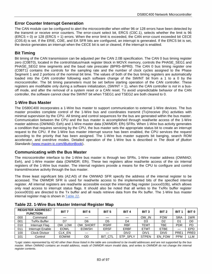
DS80C400 Network Microcontroller
83 of 97
Error Counter Interrupt Generation The CAN module can be configured to alert the microcontroller when either 96 or 128 errors have been detected by the transmit or receive error counters. The error-count select bit, ERCS (C0C.1), selects whether the limit is 96 (ERCS = 0) or 128 (ERCS = 1) errors. When the error limit is exceeded, the CAN error-count exceeded bit CECE (C0S.6) is set. If the ERIE, C0IE, and EA SFR bits are configured, an interrupt is generated. If the ERCS bit is set, the device generates an interrupt when the CECE bit is set or cleared, if the interrupt is enabled. Bit Timing Bit timing of the CAN transmission can be adjusted per the CAN 2.0B specification. The CAN 0 bus timing register zero (C0BT0), located in the control/status/mask register block in MOVX memory, controls the PHASE_SEG1 and PHASE_SEG2 time segments and the baud rate prescaler (BPR5–BPR0). The CAN 0 bus timing register one (C0BT1) contains the controls for the sampling rate and the number of clock cycles assigned to the Phase Segment 1 and 2 portions of the nominal bit time. The values of both of the bus timing registers are automatically loaded into the CAN controller following each software change of the SWINT bit from a 1 to a 0 by the microcontroller. The bit timing parameters must be set before starting operation of the CAN controller. These registers are modifiable only during a software initialization, (SWINT = 1), when the CAN controller is not in a bus-off mode, and after the removal of a system reset or a CAN reset. To avoid unpredictable behavior of the CAN controller, the software cannot clear the SWINT bit when TSEG1 and TSEG2 are both cleared to 0. 1-Wire Bus Master The DS80C400 incorporates a 1-Wire bus master to support communication to external 1-Wire devices. The bus master provides complete control of the 1-Wire bus and coordinates transmit (Tx)/receive (Rx) activities with minimal supervision by the CPU. All timing and control sequences for the bus are generated within the bus master. Communication between the CPU and the bus master is accomplished through read/write access of the 1-Wire master address (OWMAD; Eeh) and 1-Wire master data (OWMDR; Efh) SFRs. When 1-Wire bus activity generates a condition that requires servicing by the CPU, the bus master sets the appropriate status bit to create an interrupt request to the CPU. If the 1-Wire bus master interrupt source has been enabled, the CPU services the request according to the priority that has been assigned. The 1-Wire bus master supports bit banging, search ROM accelerator, and overdrive modes. Detailed operation of the 1-Wire bus is described in The Book of iButton Standards (www.maxim-ic.com/iButtonBook). Communicating with the Bus Master The microcontroller interface to the 1-Wire bus master is through two SFRs, 1-Wire master address (OWMAD; Eeh), and 1-Wire master data (OWMDR; Efh). These two registers allow read/write access of the six internal registers of the 1-Wire bus master. The internal registers provide a means for the CPU to configure and control transmit/receive activity through the bus master.
The three least significant bits (A2:A0) of the OWMAD SFR specify the address of the internal register to be accessed. The OWMDR SFR is used for read/write access to the implemented bits of the specified internal register. All internal registers are read/write accessible except the interrupt flag register (xxxxx010b), which allows only read access to interrupt status flags. It should also be noted that all writes to the Tx/Rx buffer register (xxxxx001b) are directed to the Tx buffer and all reads retrieve data from the Rx buffer. The 1-Wire bus master internal register map is shown in Table 22. Table 22. 1-Wire Bus Master Internal Register Map
REGISTER ADDRESS*/ FUNCTION BIT 7 BIT 6 BIT 5 BIT 4 BIT 3 BIT 2 BIT 1 BIT 0
000 Command — — — — OW_IN FOW SRA 1WR 001 Tx/Rx Buffer D7 D6 D5 D4 D3 D2 D1 D0 010 Interrupt Flag OW_LOW OW_SHORT RSRF RBF TEMT TBE PDR PD 011 Interrupt Enable EOWL EOWSH ERSF ERBF ETMT ETBE — EPD 100 Clock Divisor CLK_EN — — DIV2 DIV1 DIV0 PRE1 PRE0 101 Control EOWMI OD BIT_CTL STP_SPLY STPEN EN_FOW PPM LLM
*Logic states represented by A2:A0 other than those listed in the table are considered to be invalid addresses and are not supported by the bus master. When OWMAD contains an invalid address, reads of OWMDR return invalid data, and writes to OWMDR do not change the internal register contents.

DS80C400 Network Microcontroller
84 of 97
Clock Control All 1-Wire timing patterns are generated using a base clock of 1.0MHz. To create this base clock frequency for the 1-Wire bus master, the microcontroller system clock must be internally divided down. The clock divisor internal register implements bits to control this clock division and generation. The prescaler bits (PRE1:PRE0) divide the microcontroller system clock by 1, 3, 5, or 7 for settings of 00b, 01b, 10b, and 11b respectively. The divider bits (DIV2:DIV0) control the circuitry, which then divides the prescaler output clock by 1, 2, 4, 8, 16, 32, 64, or 128. The CLK_EN bit (bit 7 of the clock divisor register) enables or disables the clock generation circuitry. Setting CLK_EN to a logic 1 enables the clock generation circuitry while clearing the bit disables the clock generation circuitry. The clock divisor register must be configured properly before any 1-Wire communication can take place. Table 23 shows the proper selections for the PRE1:PRE0 and DIV2:DIV0 register bits for a given microcontroller system clock. Note that the clock generation circuitry requires that the microcontroller system clock be between 3.2MHz and 75MHz, preferably with 50% duty cycle. Table 23. Clock Divisor Register Settings
SYSTEM CLOCK FREQUENCY (MHz) DIVIDER
RATIO DIV2:DIV0 DIVIDE BITS SELECTION PRE1:PRE0
PRESCALER BITS
SELECTION MIN MAX 4.0 < 5.0 4 010 4 00 1 5.0 < 6.0 5 000 1 10 5 6.0 < 7.0 6 001 2 01 3 7.0 < 8.0 7 000 1 11 7 8.0 < 10.0 8 011 8 00 1
10.0 < 12.0 10 001 2 10 5 12.0 < 14.0 12 010 4 01 3 14.0 < 16.0 14 001 2 11 7 16.0 < 20.0 16 100 16 00 1 20.0 < 24.0 20 010 4 10 5 24.0 < 28.0 24 011 8 01 3 28.0 < 32.0 28 010 4 11 7 32.0 < 40.0 32 101 32 00 1 40.0 < 48.0 40 011 8 10 5 48.0 < 56.0 48 100 16 01 3 56.0 < 64.0 56 011 8 11 7 64.0 75.0 64 110 64 00 1
Transmitting and Receiving Data All data transmitted and received by the 1-Wire bus master passes through the transmit/receive data buffer (internal register address xxxxx001b). The data buffer is double-buffered with separate transmit and receive buffers. Writing to the data buffer connects the transmit buffer to the data bus while reading connects the receive buffer to the data bus.
The data buffer combination for the transmit interface is composed of the transmit buffer and transmit shift register. Each of these registers has a flag that can be used as an interrupt source. The transmit buffer empty (TBE) flag is set when the transmit buffer is empty and ready to accept a new byte of data from the user. As soon as the data byte is written into the transmit buffer, TBE is cleared. The transmit shift register empty (TEMT) flag is set when the shift register has no data and is ready to load a new data byte from the transmit buffer. When a byte of data is transferred into the transmit shift register, TEMT is cleared and TBE becomes set.
To send a byte of data on the 1-Wire bus, the user writes the desired data to the transmit buffer. The data is moved to the transmit shift register, where it is shifted serially onto the 1-Wire bus, least significant bit first. When the transmit shift register is empty, new data is transferred from the transmit buffer (if available) and the serial process repeats. Note that the 1-Wire protocol requires a reset before any bus communication.
The data buffer combination for the receive interface is composed of the receive buffer and the receive shift register. The receive registers can also generate interrupts. The receive shift register full (RSRF) flag is set at the start of data being shifted into the register, and is cleared when the receive shift register is empty. The receive buffer full (RBF) flag is set when data is transferred from the receive shift register into the receive buffer and is cleared after the CPU reads the register. If RBF is set, and another byte of data is received in the receive shift

DS80C400 Network Microcontroller
85 of 97
register, the receive shift register holds the new byte and waits until the user reads the receive buffer, clearing the RBF flag. Thus, if both RSRF and RBF are set, no further transmissions should be made on the 1-Wire bus, or else data can be lost, as the byte in the receive shift register is overwritten by the next received data.
To read data from a slave device, the bus master must first be ready to transmit data depending on commands in the command register already set up by the CPU. Data is retrieved from the bus in a similar fashion to a write operation. The CPU initiates a read operation by writing FFh data to the transmit buffer. The data that is then shifted into the receive shift register is the wired-AND of the bus master write data (FFh) and the data from the slave device. When the receive shift register is full, the data is transferred to the receive buffer (if RBF = 0), where it can be read by the CPU. Additional bytes can be read by sending FFh again. If the slave device is not ready to respond to read request, the data received the by the bus master is identical to that which was transmitted (FFh). Bus Master Commands The 1-Wire bus master can generate special commands on the 1-Wire bus in addition to transmitting and receiving data. These commands are generated through the setting of a corresponding bit in the command register (xxxxx000h). These operational modes are defined in The Book of iButton Standards available on our website at www.maxim-ic.com/iButtonBook. 1WR (Bit 0): 1-Wire Reset. Setting this bit to logic 1 causes a reset of the 1-Wire bus, which must precede any command given on the bus. Setting this bit also automatically clears the SRA bit. The 1WR bit is automatically cleared as soon as the 1-Wire bus reset completes. The bus master sets the presence-detect interrupt flag (PD) when the reset is completed and sufficient time for a 1-Wire reset to occur has passed. The result of the 1-Wire reset is placed in the interrupt register bit PDR. If a presence-detect pulse was received, PDR is cleared; otherwise, it is set.
SRA (Bit 1): Search ROM Accelerator. Setting this bit to logic 1 places the bus master into search-ROM-accelerator mode in order to expedite the search ROM process. The general principle of the search ROM process is to deselect one device after another at every conflicting ROM ID bit position of the attached slave devices. Using the search ROM process, the bus master can ultimately learn the ROM ID for each device attached to the 1-Wire bus. To prevent the CPU from having to perform many bit manipulations during a search ROM process, the search-ROM-accelerator mode can be invoked, allowing the CPU to send 16 bytes of data to complete a single search ROM pass. Details about the search ROM algorithm can be found in The Book of iButton Standards or the High-Speed Microcontroller User’s Guide: Network Microcontroller Supplement.
FOW (Bit 2): Force OW Line Low. Setting this bit to logic 1 forces the OW line to a low value if the EN_FOW bit in the control register is also set to logic 1. The FOW bit has no affect on the OW line when the EN_FOW bit is cleared to logic 0.
OW_IN (Bit 3): OW Line Input. This bit always reflects the current logic state of the OW line. Bus Master Controls The 1-Wire bus master can perform certain special functions to support OW line operation. These special functions can be configured through the control register (xxxxx101h).
LLM (Bit 0): Long Line Mode. This bit is used to enable the long-line mode timing. Setting this bit to logic 1 effectively moves the ‘write one’ release and data-sample timing during standard mode communication out to 8µs and 22µs, respectively. The recovery time is extended to 14µs. This provides a less strict environment for long line transmissions. Clearing this bit to logic 0 leaves the ‘write one’ release, data sampling, and recovery time (during standard mode communication) at 5µs, 15µs, and 10µs, respectively.
PPM (Bit 1): Presence Pulse Masking. This bit is used to enable/disable the presence pulse-masking function. Setting this bit to logic 1 causes the bus master to initiate the beginning of a presence pulse during a 1-Wire reset. This enables the master to prevent the larger amount of ringing caused by slave devices pulling the OW line low. If the PPM bit is set, the PDR result bit in the interrupt flag register is always set, indicating that a slave device is present on the OW line (even if there are none). Clearing the PPM bit to logic 0 disables the presence pulse-masking function.
DS80C400 Network Microcontroller
86 of 97
EN_FOW (Bit 2): Enable Force OW. Setting the EN_FOW bit to a logic 1 allows the bus master to force the OW line low using FOW (bit 2 of the command register). Clearing the EN_FOW bit to a logic 0 disables the use of the FOW bit.
STPEN (Bit 3): Strong Pullup Enable. Setting the STPEN bit to a logic 1 enables functionality for the OWSTP output pin. The OWSTP pin serves as the enable signal to an external strong pullup device. This functionality is used for meeting the recovery time requirement in overdrive mode and long-line standard communication. When enabled (STPEN = 1), OWSTP goes active-low any time the master is not pulling the OW line low or waiting to read data from a slave during a communication sequence. Once the communication sequence is complete, the OWSTP output is released. Note that when the master is in the idle state, the STP_SPLY bit must also be set to logic 1 (in addition to STPEN = 1) in order for the OWSTP pin to remain in the active-low state. Clearing the STPEN bit to logic 0 disables all OWSTP pin functionality.
STP_SPLY (Bit 4): Strong Pullup Supply Mode. When the OWSTP pin is enabled (STPEN = 1), setting the STP_SPLY bit to logic 1 results in an active-low output for the OWSTP pin being sustained when the master is in an idle state. Thus, when the OWSTP signal gates an external P-channel pullup, STP_SPLY = 1 can be used to enable a stiff supply voltage to slave devices requiring high current during operation. Clearing the bit to logic 0 disables the strong pullup on the OWSTP pin when the master is idle. This bit has no affect when the OWSTP pin is disabled (STPEN = 0).
BIT_CTL (Bit 5): Bit-Banging Mode. Setting this bit to logic 1 place the master into the bit-banging mode of operation. In the bit-banging mode, only the least significant bit of the transmit/receive register is sent or received before the associated interrupt flag occurs (signaling the end of the transaction). Clearing the bit leaves the bus master operating in full-byte boundaries.
OD (Bit 6): Overdrive Mode. Setting this bit to a logic 1 places the master into overdrive mode, effectively changing the bus master timing to match the 1-Wire timing for overdrive mode as outlined in The Book of iButton Standards. Clearing the OD bit to a logic 0 leaves the master operating with standard mode timing.
EOWMI (Bit 7): Enable 1-Wire Master Interrupt. Setting this bit to a logic 1 enables the 1-Wire master interrupt request to the CPU for any of the 1-Wire interrupt sources that have been individually enabled in the interrupt enable register (xxxxx011b). Since the 1-Wire master interrupt and external interrupt 5 share the same interrupt flag (IE5; EXIF.7), both cannot be used simultaneously. Thus, enabling the 1-Wire interrupt source effectively disables the external interrupt 5 source. 1-Wire Interrupts The 1-Wire bus master can be configured to generate an interrupt request to the CPU on the occurrence of a number of 1-Wire-related events or conditions. These include the following: presence-detect, transmit buffer empty, transmit shift-register empty, receive buffer full, receive shift-register full, 1-Wire short, and 1-Wire low. Each of these potential 1-Wire interrupt sources has a corresponding enable bit and flag bit. Each flag bit in the interrupt flag register (xxxxx010b) is set, independent of the interrupt enable bit, when the associated event or condition occurs. In order for the interrupt flag to generate an interrupt request to the CPU, however, the individual enable bit for the source along with the 1-Wire bus master interrupt enable bit (EOWMI; control register bit 7), and global interrupt enable bit (EA; IE.7) must both be set to a logic 1. To clear the 1-Wire bus master interrupt, a read of the interrupt flag register must always be performed by software. Table 24 summarizes the 1-Wire bus master interrupt sources.
DS80C400 Network Microcontroller
87 of 97
Table 24. 1-Wire Bus Master Interrupt Sources INTERRUPT
SOURCE MEANING ENABLE/FLAG LOCATION
(Interrupt Flag Register.x Interrupt Enable Register.x)
Presence Detect After a 1-Wire reset has been issued, this flag is set after the amount of time for a presence-detect pulse to have occurred. This bit is cleared when the interrupt flag register is read.
Bit 0
Transmit Buffer Empty
This flag is set when the transmit buffer is empty and ready to receive the next byte. This bit is cleared when data is written to the transmit buffer. A read of the interrupt flag register has no effect on this bit.
Bit 2
Transmit Shift Register Empty
This flag is set when the transmit shift register is empty and is ready to load a new byte from the transmit buffer. This bit is cleared when data is transferred from the transmit buffer to the transmit shift register. A read of the interrupt flag register has no effect on this bit.
Bit 3
Receive Buffer Full This flag is set when there is a byte of data in the receive buffer waiting to be read. This bit is cleared when the receive buffer is read. Bit 4
Receive Shift Register Full
This flag is set when there is a byte of data in the receive shift register waiting to be transferred to the receive buffer. This bit is cleared when data in the receive shift register is transferred to the receive buffer.
Bit 5
1-Wire Short This flag is set when the OW line was low before the bus master was able to send out the beginning of a reset or a time slot. A read of the interrupt flag register clears this bit.
Bit 6
1-Wire Low
This flag is set when the OW line is low while the bus master is idle, signaling that a slave device has issued a presence pulse on the OW line. A read of the interrupt flag register clears this bit if the OW line is no longer low while the master is idle.
Bit 7
Peripheral Overview (Primary Integrated System Logic) The DS80C400 provides several of the most commonly needed peripheral functions in microcomputer-based systems. The DS80C400 offers three serial ports, four timers, a programmable watchdog timer, power-fail reset detection, and a power-fail interrupt flag. In addition, the microcontroller contains a CAN module for industrial communication applications. Each of these peripherals is described below, and more details are available in the High-Speed Microcontroller User’s Guide and the High-Speed Microcontroller User’s Guide: Network Microcontroller Supplement. Serial Ports The microcontroller provides a serial port (UART) that is identical to the 80C52. Two additional hardware serial ports are provided that are duplicates of the first one. This second port optionally uses pins P1.2 (RXD1) and P1.3 (TXD1). The third port optionally uses pins P6.6 (RXD2) and P6.7 (TXD2). The function of each of the three serial ports is controlled by the SFRs and bits shown in Table 25. Table 25. Serial Port SFRs
SERIAL PORT FUNCTION CONTROL SERIAL PORT 0 SERIAL PORT 1 SERIAL PORT 2
Control Register SCON0 SCON1 SCON2 Input/Output Data Buffer SBUF0 SBUF1 SBUF2 Baud Rate Doubler Bit PCON.7 WDCON.7 T3CM.4
Framing Error-Detection Enable PCON.6 PCON.6 PCON.6 Slave Address Mask Enable SADEN0 SADEN1 SADEN2
Slave Address SADDR0 SADDR1 SADDR2 All three serial ports can operate simultaneously and be configured for different baud rates or different modes. When using a timer for the purpose of baud rate generation, serial port 1 must use timer 1, serial port 2 must use timer 3, while serial port 0 can use either timer 1 or timer 2. Refer to the High-Speed Microcontroller User Guide for full descriptions of serial port operational modes.

DS80C400 Network Microcontroller
88 of 97
Timers The microcontroller provides four general-purpose timer/counters. Timers 0, 1, and 3 have three common modes of operation. Each of the three can be used as a 13-bit timer/counter, 16-bit timer/counter, or 8-bit timer/counter with auto-reload. Timer 0 can also operate as two 8-bit timer/counters. When operated as a counter, timers 0, 1, and 3 count pulses on the corresponding T0, T1, and T3 external pins. Timer 2 is a true 16-bit timer/counter with several additional operating modes. With a 16-bit reload register, timer 2 supports other features such as 16-bit auto-reload, capture, up/down count, and output clock generation. All four timer/counters default to the standard oscillator frequency divided by 12 input clock but can be configured to run from the system clock divided by 4. Timers 1 and 2 can also be configured to operate with an input clock equal to the system clock divided by 13. Table 26 shows the SFRs and bits associated with the four timer/counters. Table 26. Timer/Counter SFRs
TIMER/COUNTER FUNCTION TIMER/ COUNTER 0
TIMER/ COUNTER 1
TIMER/ COUNTER 2
TIMER/ COUNTER 3
Timer/Counter Mode Selection and Control TMOD, TCON TMOD, TCON T2MOD, T2CON T3CM
Count Registers TH0, TL0 TH1, TL1 TH2, TL2 TH3, TL3 8-Bit Reload Register TH0 TH1 — TH3
16-Bit Reload/Capture Registers — — RCAP2H, RCAP2L —
Timer Input Clock-Select Bit CKCON.3 CKCON.4 CKCON.5 T3CM.5 Divide-by-13 Clock-Option Bit — T2MOD.4 T2MOD.3 —
Watchdog Timer The watchdog is a free-running, programmable timer that can set a flag, cause an interrupt, and/or reset the microcontroller if allowed to reach a preselected timeout. It can be restarted by software. A typical application uses the watchdog timer as a reset source to prevent software from losing control. The watchdog timer is initialized, selecting the timeout period and enabling the reset and/or interrupt functions. After enabling the reset function, software must then restart the timer before its expiration or hardware resets the CPU. In this way, if the code execution goes awry and software does not reset the watchdog as scheduled, the microcontroller is put in reset, a known good state. Software can select one of four timeout values as controlled by the WD1 and WD0 bits. Timeout values are precise since they are a function of the crystal frequency. When the watchdog times out, the watchdog interrupt flag (WDIF = WDCON.3) is set. If the watchdog interrupt source has been enabled, program execution immediately vectors to the watchdog timer interrupt-service routine (code address = 63h). To enable the watchdog interrupt source, both the EWDI (EIE.4) and EA (IE.7) bits must be set. Furthermore, setting the EWT (WDCON.1) bit allows the watchdog timer to generate a reset exactly 512 system clocks following a timeout. To prevent the watchdog reset from occurring in such a situation, the watchdog timer count must be reset (RWT = 1) or the watchdog-reset function itself must be disabled (EWT = 0). Both the enable watchdog timer (EWT) reset and the reset watchdog timer (RWT) control bits are protected by timed-access circuitry. This prevents errant software from accidentally clearing or disabling the watchdog. When a watchdog timer reset condition occurs, the watchdog timer reset flag (WTRF = WDCON.2) is set by the hardware. This flag can then be interrogated following a reset to determine whether the reset was caused by the watchdog timer. The watchdog interrupt is useful for systems that do not require a reset circuit. It sets the WDIF (watchdog interrupt) flag 512 system clocks before setting the reset flag. Software can optionally enable this interrupt source, which is independent of the watchdog-reset function. The interrupt is commonly used during the debug process to determine where watchdog reset commands must be located in the application software. The interrupt also can serve as a convenient time-base generator or can wake up the microcontroller from power-saving modes. The watchdog timer is controlled by the clock control (CKCON) and the watchdog control (WDCON) SFRs. CKCON.7 and CKCON.6 are WD1 and WD0 respectively, and they select the watchdog timeout period. Of course, the 4X/2X (PMR.3) and CD1:0 (PMR.7:6) system clock control bits also affect the timeout period. Table 27 shows the selection of timeout.

DS80C400 Network Microcontroller
89 of 97
Table 27 demonstrates that, for a 40MHz crystal frequency, the watchdog timer is capable of producing timeout periods from 3.28ms (217 x 1/40MHz) to greater than one and a half seconds (1.68 = 226 x 1/40MHz) with the default setting of CD1:0 (= 10). This wide variation in timeout periods allows very flexible system implementation. In a typical initialization, the user selects one of the possible counter values to determine the timeout. Once the counter chain has completed a full count, hardware sets the interrupt flag (WDIF = WDCON.3). Regardless of whether the software makes use of this flag, there are then 512 system clocks left until the reset flag (WTRF = WDCON.2) is set. Software can enable (1) or disable (0) the reset using the enable watchdog timer reset (EWT = WDCON.1) bit. Table 27. Watchdog Timeout Values
4X/2X CD1:0 WATCHDOG INTERRUPT TIMEOUT WD1:0 = 00 WD1:0 = 01 WD1:0 = 10 WD1:0 = 11
1 00 215 218 221 224 0 00 216 219 222 225 x 01 217 220 223 226 x 10 217 220 223 226 x 11 225 228 231 234
IrDA Clock The DS80C400 has the ability to generate an output clock (CLKO) as a secondary function on port pin P3.5. Setting both the IrDA clock-output enable bit (IRDACK:COR.7) and external clock-output enable bit (XCLKOE:COR.1) to a logic 1 produces an output clock of 16 times the programmed baud rate for serial port 0. This 16X output clock used in conjunction with serial port 0 I/O (TXD0, RXD0) conveniently allows for direct connection to common IrDA encoder/decoder devices. If the XCLKOE bit alone is set to logic 1, the CLKO pin outputs the system clock frequency divided by 2, 4, 6, or 8 as defined by clock-output divide bits (COD1:0). Setting the IRDACK bit alone to logic 1 has no effect. Interrupts The microcontroller provides 16 interrupt sources with three priority levels. All interrupts, with the exception of the power-fail interrupt, are controlled by a series combination of individual enable bits and a global interrupt enable EA (IE.7). Setting EA to a 1 allows individual interrupts to be enabled. Clearing EA disables all interrupts regardless of their individual enable settings. The three available priority levels are low, high, and highest. The highest priority level is reserved for the power-fail interrupt only. All other interrupts have individual priority bits that when set to a 1 establish the particular interrupt as high priority. In addition to the user-selectable priorities, each interrupt also has an inherent natural priority, used to determine the priority of simultaneously occurring interrupts. The available interrupt sources, their flags, enables, natural priority, and available priority selection bits are identified in Table 28. Note that external interrupts 2–5 and the 1-Wire bus master share a common interrupt vector (43h). Also note that external interrupt 5 and the 1-Wire bus master interrupt are multiplexed to form a single interrupt request. When the 1-Wire bus master interrupt is enabled (EOWMI = 1), it takes priority over external interrupt 5. In order for external interrupt 5 request to be used, the 1-Wire bus master interrupt must be disabled (EOWMI = 0).

DS80C400 Network Microcontroller
90 of 97
Table 28. Interrupt Summary NAME FUNCTION VECTOR NATURAL
PRIORITY FLAG BIT ENABLE BIT PRIORITY CONTROL BIT
PFI Power-Fail Interrupt 33h 0 PFI (WDCON.4) EPFI (WDCON.5) N/A
INT0 External Interrupt 0 03h 1 IE0 (TCON.1) (Note 2) EX0 (IE.0) PX0 (IP.0)
TF0 Timer 0 0Bh 2 TF0 (TCON.5) (Note 1) ET0 (IE.1) PT0 (IP.1)
INT1 External Interrupt 1 13h 3 IE1 (TCON.3) (Note 2) EX1 (IE.2) PX1 (IP.2)
TF1 Timer 1 1Bh 4 TF1 (TCON.7) (Note 1) ET1 (IE.3) PT1 (IP.3)
TI0 or RI0 Serial Port 0 23h 5 RI_0(SCON0.0) ES0 (IE.4) PS0 (IP.4) TI_0(SCON0.1) TF2 Timer 2 2Bh 6 TF2(T2CON.7) ET2 (IE.5) PT2 (IP.5)
TI1 or RI1 Serial Port 1 3Bh 7 RI_1(SCON1.0) ES1 (IE.6) PS1 (IP.6) TI_1(SCON1.1) INT2 External Interrupts 2–5,
1-Wire Bus Master, Interrupt
43h 8 IE2 (EXIF.4) EX2-5 (EIE.0)
PX2-5 (EIP.0) INT3 IE3 (EXIF.5) — INT4 IE4 (EXIF.6) —
INT5/OWMI — — — IE5 (EXIF.7) (Note 3) EOWMI (Note 3)
TF3 Timer 3 4Bh 9 TF3 (T3CM.7)) ET3 (EIE.1) PT3 (EIP.1) TI2 or RI2 Serial Port 2 53h 10 IE4 (EXIF.6) ES2 (EIE.2) PS2 (EIP.2)
WPI Write Protect Interrupt 5Bh 11 WPIF (MCON2.7) EWPI (EIE.3) PWPI (EIP.3) C0I CAN0 Interrupt 6Bh 12 Various C0IE (EIE.6) C0IP (EIP.6)
EAI Ethernet Activity 73h 13 TIF (BCUC.5)
EAIE (EIE.5) EAIP (EIP.5) RIF (BCUC.4) WDTI Watchdog Timer 63h 14 WDIF (WDCON.3) EWDI (EIE.4) PWDI (EIP.4) EPMI Ethernet Power Mode 7Bh 15 EPMF (BCUC.6) EPMIE (EIE.7) EPMIP (EIP.7)
Unless marked, all flags must be cleared by the application software. Note 1: Cleared automatically by hardware when the service routine is entered. Note 2: If edge-triggered, the flag is cleared automatically by hardware when the service routine is entered. If level-triggered, the flag follows the
state of the interrupt pin. Note 3: The global 1-Wire interrupt-enable bit (EOWMI) and individual 1-Wire interrupt source enables are located in the internal 1-Wire bus
master interrupt enable register, and must be accessed through the OWMAD and OWMDR SFRs. Individual 1-Wire interrupt source flag bits that are located in the internal 1-Wire bus master Interrupt flag register are accessed in the same way.
One’s Complement Adder The DS80C400 implements a one’s complement adder to support the Internet checksum algorithm. The adder contains a 16-bit accumulator and is accessed through the one’s complement adder data (OCAD) SFR. Writing two bytes to the OCAD register initiates a summation between the 16-bit accumulator and the 16-bit value entered. When entering a new 16-bit value for summation, the MSB should be loaded first and the LSB loaded second. The calculation begins on the first machine cycle following the second write to the OCAD register and executes in a single machine cycle. This allows back-to-back writes of 16-bit data to the OCAD register for summation. The carry out bit from the high-order bit of the calculation is added back into the low-order bit of the accumulator. Reading two bytes from the OCAD register downloads the contents of the 16-bit accumulator. When reading the 16-bit accumulator through the OCAD register, the MSB is unloaded first and the LSB is unloaded second. The 16-bit accumulator is cleared to 0000h following the second read of the OCAD SFR. The following is an example sequence for producing an Internet checksum for transmission. • Read OCAD twice to make certain that the 16-bit accumulator = 0000h • Write MSB of 16-bit value to OCAD • Write LSB of 16-bit value to OCAD
DS80C400 Network Microcontroller
91 of 97
• Repeat steps 2, 3 over the message data for which the checksum is to be computed • Read MSB of 16-bit value from OCAD • One’s complement of the byte last read is the Internet checksum MSB • Read LSB of 16-bit value from OCAD • One’s complement of the byte last read is the Internet checksum LSB
Note that the computation of the Internet checksum over the message data and 16-bit checksum field should yield 0000h. Clock Control and Power Management The DS80C400 includes a number of unique features that allow flexibility in selecting system clock sources and operating frequencies. To support the use of inexpensive crystals while allowing full speed operation, a clock multiplier is included in the microcontroller’s clock circuit. Also, in addition to the standard 80C32 idle and power-down (stop) modes, the DS80C400 provides a PMM. This mode allows the microcontroller to continue instruction execution at a very low speed to significantly reduce power consumption (below even idle mode). The DS80C400 also features several enhancements to stop mode that make this extremely low-power mode more useful. Each of these features is discussed in detail below. System Clock Control As mentioned previously, the microcontroller contains special clock-control circuitry that simultaneously provides maximum timing flexibility and maximum availability and economy in crystal selection. The logical operation of the system clock divide control function is shown in Figure 20. A 3:1 multiplexer, controlled by CD1, CD0 (PMR.7-6), selects one of three sources for the internal system clock: • Crystal oscillator or external clock source • (Crystal oscillator or external clock source) divided by 256 • (Crystal oscillator or external clock source) frequency multiplied by 2 or 4 times The system clock control circuitry generates two clock signals that are used by the microcontroller. The internal system clock provides the time base for timers and internal peripherals. The system clock is run through a divide-by-4 circuit to generate the machine cycle clock that provides the time base for CPU operations. All instructions execute in one to five machine cycles. It is important to note the distinction between these two clock signals, as they are sometimes confused, creating errors in timing calculations. Setting CTM = 1 and CD1, CD0 = 00b enables the frequency multiplier, either doubling or quadrupling the frequency of the crystal oscillator or external clock source. The 4X/2X bit controls the multiplying factor, selecting twice or four times the frequency when set to 0 or 1, respectively. Enabling the frequency multiplier results in apparent instruction execution speeds of 2 or 1 clocks. Regardless of the configuration of the frequency multiplier, the system clock of the microcontroller can never be operated faster than 75MHz. This means that the maximum external clock source is 18.75MHz when using the 4X setting, and 37.5MHz when using the 2X setting. The primary advantage of the clock multiplier is that it allows the microcontroller to use slower crystals to achieve the same performance level. This reduces EMI and cost, as slower crystals are generally more available and thus less expensive. Setting CD1, CD0 = 11b enables the PMM. When placed into PMM, the incoming crystal or clock frequency is divided by 256, resulting in a machine cycle of 1024 clocks. Note that power consumption in PMM is less than idle mode. While both modes leave the power-hungry internal timers running, PMM runs all clocked functions such as timers at the rate of crystal divided by 1024, rather than crystal divided by 4. Even though instruction execution continues in PMM (albeit at a reduced speed), it still consumes less power than idle mode. As a result, there is little reason to use idle mode in new designs. The system clock and machine cycle rate changes one machine cycle after the instruction changing the control bits. Note that the change affects all aspects of system operation, including timers and baud rates. Using the switchback feature, described later, can eliminate many of the problems associated with the PMM.

DS80C400 Network Microcontroller
92 of 97
Changing the System Clock/Machine Cycle Clock Frequency The microcontroller incorporates a special locking sequence to ensure “glitch-free” switching of the internal clock signals. All changes to the CD1, CD0 bits must pass through the 10 (divide-by-4) state. For example, to change from 00 (frequency multiplier) to 11 (PMM), the software must change the bits in the following sequence: 00b => 10b => 11b. Attempts to switch between invalid states fail, leaving the CD1, CD0 bits unchanged.
The following sequence must be followed when switching to the frequency multiplier as the internal time source. This sequence can only be performed when the device is in divide-by-4 operation. The steps must be followed in this order, although it is possible to have other instructions between them. Any deviation from this order causes the CD1, CD0 bits to remain unchanged. Switching from frequency multiplier to nonmultiplier mode requires no steps other than the changing of the CD1, CD0 bits.
1) Ensure that the CD1, CD0 bits are set to 10, and the RGMD (EXIF.2) bit = 0. 2) Clear the crystal multiplier enable (CTM) bit. 3) Set the 4X/2X bit to the appropriate state. 4) Set the CTM bit. 5) Poll the CKRDY bit (EXIF.3), waiting until it is set to 1. This takes approximately 65,536 cycles of the external
crystal or clock source. 6) Set CD1, CD0 to 00. The frequency multiplier is engaged on the machine cycle following the write to these bits. Figure 20. System Clock Control Diagram
Switchback As an alternative to software changing the CD1 and CD0 clock control bits to exit PMM, the microcontroller provides hardware alternatives for automatic switchback to standard speed (divide-by-4) operation. When enabled, the switchback feature allows serial ports and interrupts to automatically switch back from divide-by-1024 (PMM) to divide-by-4 (standard speed) operation. This feature makes it very convenient to use the PMM in real-time applications.
The switchback feature is enabled by setting the SFR bit SWB (PMR.5) to a 1. Once it is enabled, and PMM is selected, two possible events can cause an automatic switchback to divide-by-4 mode. First, if an external interrupt occurs and is acknowledged, the system clock reverts from PMM to divide-by-4 mode. For example, if INT0 is enabled and the CPU is not servicing a higher priority interrupt, then switchback occurs on INT0. However, if INT0 is not enabled or the CPU is servicing a higher priority interrupt, then activity on INT0 does not cause switchback to occur.
A switchback can also occur when an enabled UART detects the start bit, indicating the beginning of an incoming serial character or when the SBUF register is loaded initiating a serial transmission. Note that a serial character’s start bit does not generate an interrupt. The interrupt occurs only on reception of a complete serial word. The automatic switchback on detection of a start bit allows hardware to return to divide-by-4 operation (and the correct baud rate) in time for a proper serial reception or transmission.

DS80C400 Network Microcontroller
93 of 97
Status The STATUS (C5h) register and STATUS1 (F7h) register provide information about interrupt and serial port activity to assist in determining if it is possible to enter PMM. The microcontroller supports three levels of interrupt priority: power-fail, high, and low. The PIP (power-fail priority interrupt status; STATUS.7), HIP (high priority interrupt status; STATUS.6), and LIP (low priority interrupt status; STATUS.5) status bits, when set to a logic 1, indicate the corresponding level is in service.
Software should not rely on a lower-priority level interrupt source to remove PMM (switchback) when a higher level is in service. Check the current priority service level before entering PMM. If the current service level locks out a desired switchback source, then it would be advisable to wait until this condition clears before entering PMM. Alternately, software can prevent an undesired exit from PMM by intentionally entering a low priority interrupt-service level before entering PMM. This prevents other low priority interrupts from causing a switchback.
Entering PMM during an ongoing serial port transmission or reception can corrupt the serial port activity. To prevent this, a hardware lockout feature ignores changes to the clock divisor bits while the serial ports are active. Serial port transmit and receive activity can be monitored through the serial port activity bits located in the STATUS and STATUS1 registers. Oscillator-Fail Detect The microcontroller contains a safety mechanism called an on-chip oscillator-fail detect circuit. When enabled, this circuit causes the microcontroller to be held in reset if the oscillator frequency falls below ~100kHz. When activated, this circuit complements the watchdog timer. Normally, the watchdog timer is initialized so that it times out and causes a reset in the event that the microcontroller loses control. In the event of a crystal or external oscillator failure, however, the watchdog timer does not function, and there is the potential to fail in an uncontrolled state. Using the oscillator-fail detect circuit forces the microcontroller to a known state (i.e., reset) even if the oscillator stops.
The oscillator-fail detect circuitry is enabled when software sets the enable bit OFDE (PCON.4) to a 1. Please note that software must use a timed-access procedure (described earlier) to write this bit. The OFDF (PCON.5) bit also sets to a 1 when the circuitry detects an oscillator failure, and the microcontroller is forced into a reset state. This bit can only be cleared to a 0 by a power-fail reset or by software. The oscillator-fail detect circuitry is not triggered when the oscillator is stopped upon entering stop mode. Power-Fail Reset The microcontroller incorporates an internal precision bandgap voltage reference and comparator circuit that provide a power-on and power-fail reset function. This circuit monitors the incoming power supply voltages (VCC1 and VCC3) and holds the microcontroller in reset if either supply is below a minimum voltage level. When power exceeds the reset threshold, a full power-on reset is performed. In this way, this internal voltage monitoring circuitry handles both power-up and power-down conditions without the need for additional external components.
Once VCC1 and VCC3 have risen above minimum voltages, VRST1 and VRST3 respectively, the device automatically restarts the oscillator for the external crystal and counts 65,536 clock cycles before program execution begins at location 0000h. This helps the system maintain reliable operation by only permitting operation when the supply voltage is in a known good state. Software can determine that a power-on reset has occurred by checking the power-on reset flag (POR;WDCON.6). Software should clear the POR bit after reading it. Power-Fail Interrupt The bandgap voltage reference that sets precise reset thresholds also generates an optional early warning power-fail interrupt (PFI). When enabled by software, the microcontroller vectors to code address 0033h if either VCC1 or VCC3 drop below VPFW1 or VPFW3, respectively. PFI has the highest priority. The PFI enable is in the watchdog control SFR (EPFI;WDCON.5). Setting this bit to logic 1 enables the PFI. Application software can also read the PFI flag at WDCON.4. A PFI condition sets this bit to a 1. The flag is independent of the interrupt enable and must be cleared by software.
DS80C400 Network Microcontroller
94 of 97
External Reset Pins The DS80C400 has both reset input (RST) and reset output (RSTOL) pins. The RSTOL pin supplies an active-low reset output when the microcontroller is reset through a high on the RST pin, a timeout of the watchdog timer, a crystal oscillator fail, or an internally detected power-fail. The timing of the RSTOL pin is dependent on the source of the reset.
RESET TYPE/SOURCE RSTOL DURATION Power-On Reset 65,536 tCLK (as described in Power Cycle Timing Characteristics) External Reset < 1.25 machine cycles Power-Fail 65,536 tCLK (as described in Power Cycle Timing Characteristics) Watchdog Timer Reset Two machine cycles Oscillator-Fail Detect 65,536 tCLK (as described in Power Cycle Timing Characteristics)
Note: When connecting the DS80C400 to an external PHY, do not connect the RSTOL to the reset of the PHY. Doing so may disable the Ethernet transmit. Idle Mode Setting the IDLE bit (PCON.0) invokes the idle mode. Idle leaves internal clocks, serial ports, and timers running. Power consumption drops because memory is not being accessed and instructions are not being executed. Since clocks are running, the idle power consumption is a function of crystal frequency. The CPU can exit idle mode with any interrupt or a reset. Because PMM consumes less power than idle mode, and leaves the timers and CPU operating, idle mode is no longer recommended for new designs, and is included for backward-software compatibility only. Stop Mode Setting the STOP bit of the power-control register (PCON.1) invokes stop mode. Stop mode is the lowest power state (besides power off) since it turns off all internal clocking. All microcontroller operation ceases at the end of the instruction that sets the STOP bit. The CPU invokes stop mode only when the CAN controller has been disabled (through the SWINT or CRST bits in the C0C SFR) and when the Ethernet controller has been placed in sleep mode. The CPU can exit stop mode through an external interrupt, Ethernet power-mode interrupt, CAN interrupt, or a reset condition. Internally generated interrupts (timer, serial port, watchdog) cannot cause an exit from stop mode because internal clocks are not active in stop mode. See the DC Electrical Specifications section for ICC1 and ICC3 maximum stop mode currents. Bandgap Select The DS80C400 provides two enhancements to stop mode. As described below, the device provides a bandgap reference to determine power-fail interrupt and reset thresholds. The bandgap reference is controlled by the bandgap select bit, BGS (EXIF.0). Setting BGS to a 1 keeps the bandgap reference enabled during stop mode. The default or reset condition of the bit is logic 0, which disables the bandgap during stop mode. This bit does not enable/disable the internal reference during full power, PMM, or idle modes.
With the bandgap reference enabled, the power-fail reset and power-fail interrupt sources are valid means for leaving stop mode. This allows software to detect and compensate for a power supply sag or brownout, even when in stop mode. When BGS = 1, the internal bandgap and associated comparator circuitry consume a small amount of additional current during stop mode. If a user does not require a power-fail reset or interrupt while in stop mode, the bandgap can remain disabled. Only the most power-sensitive applications should disable the bandgap reference in stop mode, as this results in an uncontrolled power-down condition. Ring Oscillator The second enhancement to stop mode reduces power consumption and allows the device to restart instantly when exiting stop mode. The ring oscillator is an internal clock that can optionally provide the clock source to the microcontroller when exiting stop mode in response to an interrupt.
During stop mode the crystal oscillator is halted to maximize power savings. Typically 1ms to 7ms are required for an external crystal to begin oscillating again once the device receives the exit stimulus. The ring oscillator, by contrast, is a free-running digital oscillator that has no startup delay. The ring oscillator feature is enabled by setting the ring oscillator select bit, RGSL (EXIF.1). If enabled, the microcontroller uses the ring oscillator as the clock

DS80C400 Network Microcontroller
95 of 97
source to exit stop mode, resuming operation in less than 100ns. After 65,536 oscillations of the external clock source (not the ring oscillator), the device clears the ring oscillator mode bit, RGMD (EXIF.2), to indicate that the device has switched from the ring oscillator to the external clock source.
The ring oscillator runs at approximately 15MHz, but varies over temperature and voltage. As a result, no serial communication or precision timing should be attempted while running from the ring oscillator, since the operating frequency is not precise. Likewise, the Ethernet and CAN controllers derive their timing from the system clock and should not be enabled until RGMD = 0. The reset (default) state of the RGSL bit is logic 0, which does not result in use of the ring oscillator to exit stop mode. EMI Reduction One of the major contributors to radiated noise in an 8051-based system is the toggling of ALE. The microcontroller allows software to disable ALE when not used by setting the ALEOFF (PMR.2) bit to a 1. When ALEOFF = 1, ALE automatically toggles during off-chip program and data memory accesses. However, ALE remains static when performing on-chip memory access. The default state of ALEOFF is 0, so ALE normally toggles at a frequency of XTAL/4. Software Breakpoint Mode The DS80C400 provides a special software-breakpoint mode for code-debug purposes. Breakpoint mode can be enabled by setting the BPME bit (ACON.4) to a logic 1. Once enabled, the A5h op code can be used to create a break in code execution. When the break op code (A5h) is executed, all clocks to the timer 0, 1, 2, 3, and watchdog timer blocks are stopped and any serial port operation (when derived from a timer) is halted. Additionally, the state machine controlling access to timed-access-protected SFRs is suspended. Much like an interrupt, the CPU generates a hardware LCALL and vector to address location 000083h. Unlike an interrupt, however, the return address is not pushed onto the stack, but is placed into the BPA1 (LSB), BPA2 (MSB), and BPA3 (XSB) SFRs, and the A5h op code is used to exit breakpoint mode and return to the address contained in the BPA3:1 SFRs.
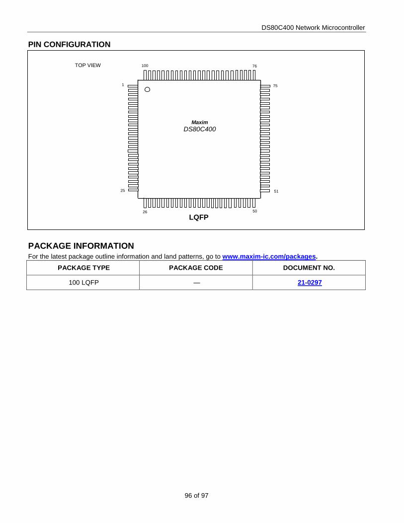
DS80C400 Network Microcontroller
96 of 97
PIN CONFIGURATION PACKAGE INFORMATION For the latest package outline information and land patterns, go to www.maxim-ic.com/packages.
PACKAGE TYPE PACKAGE CODE DOCUMENT NO.
100 LQFP — 21-0297
TOP VIEW 100 76
50 26
1
Maxim DS80C400
75
51 25
LQFP

DS80C400 Network Microcontroller
97 of 97 Maxim cannot assume responsibility for use of any circuitry other than circuitry entirely embodied in a Maxim product. No circuit patent licenses are implied. Maxim reserves the right to change the circuitry and specifications without notice at any time. Maxim Integrated Products, 160 Rio Robles, San Jose, CA 95134 408-601-1000 © 2015 Maxim Integrated Products Maxim is a registered trademark of Maxim Integrated Products, Inc.
REVISION HISTORY REVISION NUMBER
REVISION DATE DESCRIPTION PAGES
CHANGED 0 111202 New product release. —
1 060203
Replaced “DS2502U-E48” with “DS2502-E48.” 69, 72
MOVX Characteristics (Nonmultiplexed Address/Data Bus) table: Moved MIN spec for tPXIZ to MAX column.
14
Added note for connecting the PHY to the DS80C400: “When connecting the DS80C400 to an external PHY, do not connect the RSTOL to the reset of the PHY. Doing so may disable the Ethernet transmit.”
29, 49, 60, 94
Updated Figure 12: ROM Code Boot Sequence flowchart. 70
2 102103 Corrected PSEN signal in the “Nonmultiplexed, 2-Cycle Data Memory CE0-7 Write” timing diagram. 18
Corrected PT2/PT3 references in Table 21 and Table 28. 82, 90
3 111704
Clarified where appropriate the operation of the device when ROM is disabled; clarified the system requirements when using TINI ROM firmware.
33, 40, 41, 42, 47, 51, 52, 69, 71, 73, 74, 75,
79
Modified Figure 12: ROM Code Boot Sequence to better explain action of the DS80C400 when it is searching for ROM code. 70
High-Speed Microcontroller User’s Guide: DS80C400 Supplement was changed to High-Speed Microcontroller User’s Guide: Network Microcontroller Supplement in all instances.
1, 34, 72, 75, 78, 79, 80,
85, 87
4 060805 Added lead-free part to Ordering Information table. 1
5 010907
Added notes explaining that the system clock must be > 25MHz to support Ethernet 100Mbps mode. 49, 69
Corrected BCUD SFR address in Buffer Control Unit section. 50
Updated package drawing. 97
6 061908
In the Pin Description, replaced the Port 4 description to match the SFR description in the High-Speed Microcontroller User’s Guide: Network Microcontroller Supplement.
30
Updated Figure 12 to clarify operation when no user code was found. 70
7 6/09 Corrected the SEL (DPS.3) bit reset state from 1 to 0 in Table 2. 38
8 4/15 Removed automotive reference from the Controller Area Network (CAN) Module section 79