
DrMOS Integrated Power Stage - Vishay · SiC770CD Vishay Siliconix S13-1119-Rev. A, 27-May-13 1...
13
SiC770CD www.vishay.com Vishay Siliconix S13-1119-Rev. A, 27-May-13 1 Document Number: 62727 For technical questions, contact: [email protected] THIS DOCUMENT IS SUBJECT TO CHANGE WITHOUT NOTICE. THE PRODUCTS DESCRIBED HEREIN AND THIS DOCUMENT ARE SUBJECT TO SPECIFIC DISCLAIMERS, SET FORTH AT www.vishay.com/doc?91000 DrMOS Integrated Power Stage DESCRIPTION The SiC770 is an integrated power stage solution optimized for synchronous buck applications to offer high current, high efficiency and high power density performance. Packaged in Vishay’s proprietary 6 mm x 6 mm MLP package, SiC770 enables voltage regulator design to deliver in excess of 40 A per phase current. The internal power MOSFETs utilizes Vishay’s state-of-the-art TrenchFET Gen IV technology that delivers industry bench-mark performance to significantly reduce switching and conduction losses. The SiC770 incorporates an advanced MOSFET gate driver IC that features high current driving capability, adaptive dead-time control, and integrated bootstrap Schottky diode, a thermal warning (THWn) alerts the system of excessive junction temperature. This driver is also compatible with wide range of PWM controllers with the support of tri-state PWM, 5 V PWM logic, and skip mode (ZCD) for improve light load efficiency. FEATURES • Industry benchmark MOSFET with integrated Schottky diode • Delivers in excess of 40 A continuous current • 91 % peak efficiency • High frequency operation up to 1 MHz • Power MOSFETs optimized for 19 V input stage • 5 V PWM logic with tri-state and hold-off • Automatic skip mode operation (ZCD) for light load efficiency • Built-in bootstrap Schottky diode • Thermal monitor flag •V CIN under voltage lockout • Compliant with Intel DrMOS 4.0 specification • Thermally enhanced PowerPAK ® MLP6x6-40L package • Material categorization: For definitions of compliance please see www.vishay.com/doc?99912 APPLICATIONS • Synchronous buck converters • Muliti-phase VRDs for CPU, GPU and memory • DC/DC POL modules TYPICAL APPLICATION DIAGRAM Fig. 1 - SiC770 Typical Application Diagram PWM Controller Gate Driver 5V VIN VOUT VCIN ZCD_EN# DSBL # PWM THWn VDRV GH VIN BOOT SW PGND GL CGND PHASE
Transcript of DrMOS Integrated Power Stage - Vishay · SiC770CD Vishay Siliconix S13-1119-Rev. A, 27-May-13 1...

SiC770CDwww.vishay.com Vishay Siliconix
S13-1119-Rev. A, 27-May-13 1 Document Number: 62727
For technical questions, contact: [email protected] DOCUMENT IS SUBJECT TO CHANGE WITHOUT NOTICE. THE PRODUCTS DESCRIBED HEREIN AND THIS DOCUMENT
ARE SUBJECT TO SPECIFIC DISCLAIMERS, SET FORTH AT www.vishay.com/doc?91000
DrMOS Integrated Power Stage
DESCRIPTIONThe SiC770 is an integrated power stage solution optimizedfor synchronous buck applications to offer high current, highefficiency and high power density performance. Packagedin Vishay’s proprietary 6 mm x 6 mm MLP package, SiC770enables voltage regulator design to deliver in excess of 40 Aper phase current.
The internal power MOSFETs utilizes Vishay’sstate-of-the-art TrenchFET Gen IV technology that deliversindustry bench-mark performance to significantly reduceswitching and conduction losses.
The SiC770 incorporates an advanced MOSFET gate driverIC that features high current driving capability, adaptivedead-time control, and integrated bootstrap Schottkydiode, a thermal warning (THWn) alerts the system ofexcessive junction temperature. This driver is alsocompatible with wide range of PWM controllers with thesupport of tri-state PWM, 5 V PWM logic, and skip mode(ZCD) for improve light load efficiency.
FEATURES• Industry benchmark MOSFET with integrated
Schottky diode
• Delivers in excess of 40 A continuous current
• 91 % peak efficiency
• High frequency operation up to 1 MHz
• Power MOSFETs optimized for 19 V input stage
• 5 V PWM logic with tri-state and hold-off
• Automatic skip mode operation (ZCD) for light loadefficiency
• Built-in bootstrap Schottky diode
• Thermal monitor flag
• VCIN under voltage lockout
• Compliant with Intel DrMOS 4.0 specification
• Thermally enhanced PowerPAK® MLP6x6-40L package
• Material categorization: For definitions of complianceplease see www.vishay.com/doc?99912
APPLICATIONS• Synchronous buck converters
• Muliti-phase VRDs for CPU, GPU and memory
• DC/DC POL modules
TYPICAL APPLICATION DIAGRAM
Fig. 1 - SiC770 Typical Application Diagram
PWMController
Gate Driver
5V VIN
VOUT
VCIN
ZCD_EN#
DSBL #
PWM
THWn
VD
RV
GH
VIN
BOOT
SW
PG
ND
GL
CG
ND
PHASE

SiC770CDwww.vishay.com Vishay Siliconix
S13-1119-Rev. A, 27-May-13 2 Document Number: 62727
For technical questions, contact: [email protected] DOCUMENT IS SUBJECT TO CHANGE WITHOUT NOTICE. THE PRODUCTS DESCRIBED HEREIN AND THIS DOCUMENT
ARE SUBJECT TO SPECIFIC DISCLAIMERS, SET FORTH AT www.vishay.com/doc?91000
PINOUT CONFIGURATION
Fig. 2 - SiC770 Pin Configuration
PIN DESCRIPTIONPIN# NAME FUNCTION
1 ZCD_EN# LS FET turn-off logic; active low
2 VCIN Supply voltage for internal logic circuitry
3 VDRV Supply voltage for internal gate driver
4 BOOT High side driver bootstrap voltage
5, 37, P1 CGND Analog ground for the driver IC
6 GH High side gate signal
7 PHASE Return path of HS gate driver
8 to 14, P2 VIN Power stage input voltage. Drain of high side MOSFET
15, 29 to 35, P3 VSWH Phase node of the power stage
16 to 28 PGND Power ground
36 GL Low side gate signal
38 THWn Thermal warning open drain output
39 DSBL# Disable pin; active low
40 PWM PWM input logic
ORDERING INFORMATIONPART NUMBER PACKAGE MARKING CODE
SiC770CD-T1-GE3 PowerPAK MLP66-40L SiC770CD
SiC770DB Reference Board
ZCD_EN#
VCIN 2
VDRV 3
BOOT 4
CGND 5
GH 6
PHASE 7
VIN 8
VIN 9
VIN 10
VIN
11
VIN
12
VIN
13
VIN
14
VS
WH
15
PG
ND
16
PG
ND
17
PG
ND
18
PG
ND
19
PG
ND
20
28 PGND
27 PGND
26 PGND
25 PGND
24 PGND
23 PGND
22 PGND
21 PGND
30 VSWH
29 VSWH
31 VS
WH
32 VS
WH
33 VS
WH
34 VS
WH
35 VS
WH
36 GL
37 CG
ND
38 THW
n
39 DS
BL#
40 PW
M
CGND
VIN
VSWH
ZCD_EN#
VCIN 2
VDRV 3
BOOT 4
CGND 5
GH 6
PHASE 7
VIN 8
VIN 9
VIN 10
VIN
11
VIN
12
VIN
13
VIN
14
VS
WH
15
PG
ND
16
PG
ND
17
PG
ND
18
PG
ND
19
PG
ND
20
28 PGND
27 PGND
26 PGND
25 PGND
24 PGND
23 PGND
22 PGND
21 PGND
30 VSWH
29 VSWH
31 V
SW
H
32 V
SW
H
33 V
SW
H
34 V
SW
H
35 V
SW
H
36 G
L
37 C
GN
D
38 T
HW
n
39 D
SB
L#
40 P
WM
CGND
VIN
VSWH
SiC770CDwww.vishay.com Vishay Siliconix
S13-1119-Rev. A, 27-May-13 3 Document Number: 62727
For technical questions, contact: [email protected] DOCUMENT IS SUBJECT TO CHANGE WITHOUT NOTICE. THE PRODUCTS DESCRIBED HEREIN AND THIS DOCUMENT
ARE SUBJECT TO SPECIFIC DISCLAIMERS, SET FORTH AT www.vishay.com/doc?91000
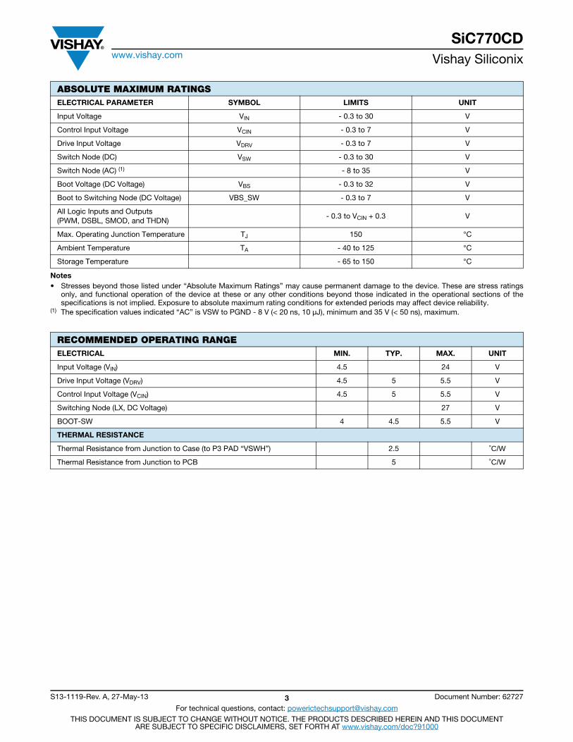
Notes• Stresses beyond those listed under “Absolute Maximum Ratings” may cause permanent damage to the device. These are stress ratings
only, and functional operation of the device at these or any other conditions beyond those indicated in the operational sections of thespecifications is not implied. Exposure to absolute maximum rating conditions for extended periods may affect device reliability.
(1) The specification values indicated “AC” is VSW to PGND - 8 V (< 20 ns, 10 μJ), minimum and 35 V (< 50 ns), maximum.
ABSOLUTE MAXIMUM RATINGSELECTRICAL PARAMETER SYMBOL LIMITS UNIT
Input Voltage VIN - 0.3 to 30 V
Control Input Voltage VCIN - 0.3 to 7 V
Drive Input Voltage VDRV - 0.3 to 7 V
Switch Node (DC) VSW - 0.3 to 30 V
Switch Node (AC) (1) - 8 to 35 V
Boot Voltage (DC Voltage) VBS - 0.3 to 32 V
Boot to Switching Node (DC Voltage) VBS_SW - 0.3 to 7 V
All Logic Inputs and Outputs (PWM, DSBL, SMOD, and THDN)
- 0.3 to VCIN + 0.3 V
Max. Operating Junction Temperature TJ 150 °C
Ambient Temperature TA - 40 to 125 °C
Storage Temperature - 65 to 150 °C
RECOMMENDED OPERATING RANGE ELECTRICAL MIN. TYP. MAX. UNIT
Input Voltage (VIN) 4.5 24 V
Drive Input Voltage (VDRV) 4.5 5 5.5 V
Control Input Voltage (VCIN) 4.5 5 5.5 V
Switching Node (LX, DC Voltage) 27 V
BOOT-SW 4 4.5 5.5 V
THERMAL RESISTANCE
Thermal Resistance from Junction to Case (to P3 PAD “VSWH”) 2.5 °C/W
Thermal Resistance from Junction to PCB 5 °C/W

SiC770CDwww.vishay.com Vishay Siliconix
S13-1119-Rev. A, 27-May-13 4 Document Number: 62727
For technical questions, contact: [email protected] DOCUMENT IS SUBJECT TO CHANGE WITHOUT NOTICE. THE PRODUCTS DESCRIBED HEREIN AND THIS DOCUMENT
ARE SUBJECT TO SPECIFIC DISCLAIMERS, SET FORTH AT www.vishay.com/doc?91000
Notes(1) Typical limits are established by characterization and are not production tested.(2) Guaranteed by design.(3) Min. and max. parameters are not 100 % production tested.
ELECTRICAL SPECIFICATIONS (DSBL# = 5 V, SMOD = 5 V, VIN = 19 V, VDRV and VCIN = 5 V, TA = 25 °C)
PARAMETER SYMBOL TEST CONDITIONS UNLESS SPECIFIED MIN. TYP. MAX. UNIT
POWER SUPPLIES
Control Logic Input Current IVCIN
VDSBL# = 0 V, no switching 21
μAVDSBL# = 5 V, no switching 350
VDSBL# = 5 V, fS = 300 kHz, D = 0.1 500
Drive Input Current (Dynamic) IVDRVfS = 300 kHz, D = 0.1 14
mAfS = 1 MHz, D = 0.1 40
BOOTSTRAP SUPPLYBootstrap Switch Forward Voltage VF VCIN = 5 V, forward bias current 2 mA 0.6 V
PWM CONTROL INPUTRising Threshold PWMTH_R 3.5 3.9 4.2 V
Falling Threshold PWMTH_F 0.8 1.0 1.2 V
Tri-state Voltage VTRI PWM pin floating 2.3 V
Tri-state Rising Threshold VTRI_TH_R 0.9 1.3 1.8 V
Tri-state Falling Threshold VTRI_TH_F 3.4 3.7 4.0 V
Tri-state Rising Threshold Hysteresis VTRI_HYS_R 280 mV
Tri-state Falling Threshold Hysteresis VTRI_HYS_F 180 mV
PWM Input Current IPWMVPWM = 5 V 250
μAVPWM = 0 V - 250
TIMING SPECIFICATIONSTri-state to GH/GL Rising Propagation Delay TPD_R_Tri
No load, see fig. 4
20 ns
Tri-state Hold-Off Time TTSHO 150 ns
GH - Turn Off Propagation Delay TPD_OFF_GH 20 ns
GH - Turn ON Propagation Delay(Dead Time Rising)
TPD_ON_GH 15 ns
GL - Turn Off Propagation Delay TPD_OFF_GL 20 ns
GL - Turn ON Propagation Delay(Dead Time Falling)
TPD_ON_GL 20 ns
DSBL# Hi to GH/GL Rising Propagation Delay TPD_R_DSBL 500 ns
DSBL# Lo to GH/GL Falling Propagation Delay TPD_F_DSBL 200 ns
DSBL# , ZCD_EN# INPUT
DSBL# Logic Input Voltage VDSBLEnable 2
VDisenable 0.8
ZCD_EN# Logic Input Voltage VSMODHigh State 2
VLow State 0.8
PROTECTION
Under Voltage Lockout VUVLORising, On Threshold 3.3 3.9
VFalling, Off Threshold 2.3 2.95
Under Voltage Lockout Hysteresis 400 mV
THWn Flag Set(2) (2) 160 °C
THWn Flag Clear(2) 135 °C
THWn Flag Hysteresis(2) 25 °C
THWn Output Low 0.02 V

SiC770CDwww.vishay.com Vishay Siliconix
S13-1119-Rev. A, 27-May-13 5 Document Number: 62727
For technical questions, contact: [email protected] DOCUMENT IS SUBJECT TO CHANGE WITHOUT NOTICE. THE PRODUCTS DESCRIBED HEREIN AND THIS DOCUMENT
ARE SUBJECT TO SPECIFIC DISCLAIMERS, SET FORTH AT www.vishay.com/doc?91000
DETAILED OPERATIONAL DESCRIPTION
PWM Input with Tri-State Function
The PWM input receives the PWM control signal from the VRcontroller IC. The PWM input is designed to be compatiblewith standard controllers using two state logic (H and L) andadvanced controllers that incorporate tri-state logic (H, L,and tri-state) on the PWM output. For two state logic, thePWM input operates as follows. When PWM is driven aboveVth_pwm_r the low side is turned OFF and the high side isturned ON. When PWM input is driven below Vth_pwm_f thehigh side turns off and the low side turns on. For tri-statelogic, the PWM input operates as above for driving theMOSFETs. However, there is an third state that is enteredinto as the PWM output of tri-state compatible controllerenters its high impedance state during shut-down. The highimpedance state of the controller’s PWM output allows theSiC770 to pull the PWM input into the tri-state region (seethe tri-state Voltage Threshold diagram below). If the PWMinput stays in this region for the tri-state hold-off period,tTSHO, both high side and low side MOSFETs are turned off.This function allows the VR phase to be disabled withoutnegative output voltage swing caused by inductor ringingand saves a schottky diode clamp. The PWM and tri-stateregions are separated by hysteresis to prevent falsetriggering. The SiC770CD incorporates PWM voltagethresholds that are compatible with 5 V logic.
Disable (DSBL#)
In the low state, the DSBL# pin shuts down the driver IC anddisables both high-side and low-side MOSFET. In this state,the standby current is minimized. If DSBL# is leftunconnected an internal pull-down resistor will pull the pindown to CGND and shut down the IC.
Diode Emulation Mode (ZCD_EN#) Skip
When ZCD_EN# pin is low the diode emulation mode isenabled. This is a non-synchronous conversion mode thatimproves light load efficiency by reducing switching losses.Conducted losses that occur in synchronous buckregulators when inductor current is negative are alsoreduced. Circuitry in the gate drive IC detects the inductorvalley current when inductor current crosses zero andautomatically stops switching the low side MOSFET. SeeZCD_EN# operation diagram for additional details. Thisfunction can be also be used for a pre-biased outputvoltage. If ZCD_EN# is left un-connected, an internal pull upresistor will pull the pin up to VCIN (logic high) to disable theZCD_EN# function.
Thermal Shutdown Warning (THWn)
The THWn pin is an open drain signal that flags the presenceof excessive junction temperature. Connect a maximum of20 k to pull this pin up to VCIN. An internal temperaturesensor detects the junction temperature. The temperaturethreshold is 160 °C. When this junction temperature isexceeded the THWn flag is set. When the junctiontemperature drops below 135 °C the device will clear theTHWn signal. The SiC770 does not stop operation when theflag is set. The decision to shutdown must be made by anexternal thermal control function.
Voltage Input (VIN)
This is the power input to the drain of the high-side PowerMOSFET. This pin is connected to the high powerintermediate BUS rail.
Switch Node (VSWH and PHASE)
The switch node VSWH is the circuit PWM regulated output.This is the output applied to the filter circuit to deliver theregulated high output for the buck converter. The PHASEpin is internally connected to the switch node VSWH. This pinis to be used exclusively as the return pin for the BOOTcapacitor. A 20 k resistor is connected between GH andPHASE to provide a discharge path for the HS MOSFET inthe event that VCIN goes to zero while VIN is still applied.
Ground connections (CGND and PGND)
PGND (power ground) should be externally connected toCGND (control signal ground). The layout of the printed circuitboard should be such that the inductance separating theCGND and PGND should be a minimum. Transient differencesdue to inductance effects between these two pins shouldnot exceed 0.5 V.
Control and Drive Supply Voltage Input (VDRV, VCIN)
VCIN is the bias supply for the gate drive control IC. VDRV isthe bias supply for the gate drivers. It is recommended toseparate these pins through a resistor. This creates a lowpass filtering effect to avoid coupling of high frequencygated rive noise into the IC.
Bootstrap Circuit (BOOT)
The internal bootstrap switch and an external bootstrapcapacitor form a charge pump that supplies voltage to theBOOT pin. An integrated bootstrap diode is incorporated sothat only an external capacitor is necessary to complete thebootstrap circuit. Connect a boot strap capacitor with oneleg tied to BOOT pin and the other tied to PHASE pin.

SiC770CDwww.vishay.com Vishay Siliconix
S13-1119-Rev. A, 27-May-13 6 Document Number: 62727
For technical questions, contact: [email protected] DOCUMENT IS SUBJECT TO CHANGE WITHOUT NOTICE. THE PRODUCTS DESCRIBED HEREIN AND THIS DOCUMENT
ARE SUBJECT TO SPECIFIC DISCLAIMERS, SET FORTH AT www.vishay.com/doc?91000
Shoot-Through Protection and Adaptive Dead Time(AST)
The SiC770 has an internal adaptive logic to avoid shootthrough and optimize dead time. The shoot throughprotection ensures that both high-side and low-sideMOSFET are not turned on the same time. The adaptivedead time control operates as follows. The HS and LS gatevoltages are monitored to prevent the one turning on untilthe other's gate voltage is sufficiently low (1.0 V), that andbuilt in delays ensure the one Power MOS is completely off,before the other can be turned on. This feature helps toadjust dead time as gate transitions change with respect tooutput current and temperature.
Under Voltage Lockout (UVLO)
During the start up cycle, the UVLO disables the gate driveholding high-side and low-side MOSFET gate low until theinput voltage rail has reached a point at which the logiccircuitry can be safely activated. The SiC770 alsoincorporates logic to clamp the gate drive signals to zerowhen the UVLO falling edge triggers the shutdown of thedevice. As an added precaution, a 20.2 k resistor isconnected between GH and PHASE to provide a dischargepath for the HS MOSFET.
FUNCTIONAL BLOCK DIAGRAM
Fig. 3 - SiC770 Functional Block Diagram
DEVICE TRUTH TABLEDSBL# SMOD PWM GH GL
Open X X L L
L X X L L
H L L L H (IL > 0), L (IL 0)
H L H H L
H H H H L
H H L L H
DSBL#
VIN
BOOT
GH
GL
ZCD_EN#
Tristate PWMPWM
PGND
ADT CNTLDCM DETECT
VSWH
VDRV
UVLO
Thermal ShutdownTHWn
PHASE
VCIN

SiC770CDwww.vishay.com Vishay Siliconix
S13-1119-Rev. A, 27-May-13 7 Document Number: 62727
For technical questions, contact: [email protected] DOCUMENT IS SUBJECT TO CHANGE WITHOUT NOTICE. THE PRODUCTS DESCRIBED HEREIN AND THIS DOCUMENT
ARE SUBJECT TO SPECIFIC DISCLAIMERS, SET FORTH AT www.vishay.com/doc?91000
PWM TIMING DIAGRAM
Fig. 4 - Definition of PWM Logic and Tri-State
PWM TIMING DIAGRAM
Fig. 5 - ZCD_EN# Operation Timing Diagram Fig. 6 - DSBL# Function Timing Diagram
PWMTH_R
PWMTH_F
PWMTri_R
PWMTri_F
PWM
GH
GL
TPD_OFF_GL TTSHO
TPD_ON_GH TPD_OFF_GH
TPD_OFF_GL
TTSHO
TPD_R_Tri
TPD_R_Tri
PWM
HG
LG
ZCD_EN# High Low
PWMController
Gate Driver
VIN
VOUT
ZCD_EN#
PWM
VINBOOT
SW
PGN
D
CG
ND
PHASE
IL Sense
CS
ZCD
IL
0 A
IL = 0A
PWM
DSBL#
GH
GL
t
PWM
DSBL#
GH
GL
t
DSBL# Hi to GH Rising propagation delay DSBL# Hi to GL Rising propagation delay
Enable
PWM
DSBL#
GH
GL
DSBL# Lo to GH Falling propagation delay
t
DSBL# Lo to GL Falling propagation delay
PWM
DSBL#
GH
GL
t
Disable
SiC770CDwww.vishay.com Vishay Siliconix
S13-1119-Rev. A, 27-May-13 8 Document Number: 62727
For technical questions, contact: [email protected] DOCUMENT IS SUBJECT TO CHANGE WITHOUT NOTICE. THE PRODUCTS DESCRIBED HEREIN AND THIS DOCUMENT
ARE SUBJECT TO SPECIFIC DISCLAIMERS, SET FORTH AT www.vishay.com/doc?91000
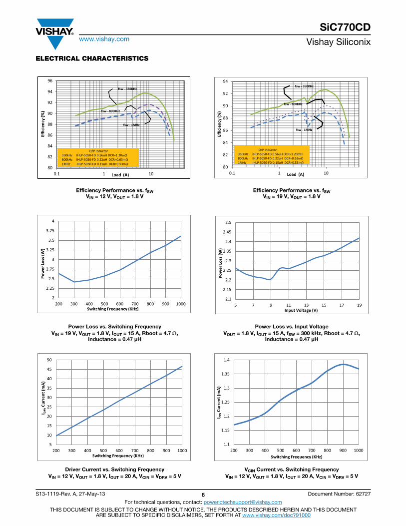
ELECTRICAL CHARACTERISTICS
Efficiency Performance vs. fSWVIN = 12 V, VOUT = 1.8 V
Power Loss vs. Switching FrequencyVIN = 19 V, VOUT = 1.8 V, IOUT = 15 A, Rboot = 4.7 ,
Inductance = 0.47 μH
Driver Current vs. Switching FrequencyVIN = 12 V, VOUT = 1.8 V, IOUT = 20 A, VCIN = VDRV = 5 V
Efficiency Performance vs. fSWVIN = 19 V, VOUT = 1.8 V
Power Loss vs. Input VoltageVOUT = 1.8 V, IOUT = 15 A, fSW = 300 kHz, Rboot = 4.7 ,
Inductance = 0.47 μH
VCIN Current vs. Switching FrequencyVIN = 12 V, VOUT = 1.8 V, IOUT = 20 A, VCIN = VDRV = 5 V
80
82
84
86
88
90
92
94
96
0.1 1 10
Effici
ency
(%)
Load (A)
O/P Inductor350kHz IHLP-5050-FD 0.56uH DCR=1.20mΩ800kHz IHLP-5050-FD 0.22uH DCR=0.63mΩ1MHz IHLP-5050-FD 0.15uH DCR=0.53mΩ
fsw - 350KHz
fsw - 800KHz
fsw - 1MHz
2
2.25
2.5
2.75
3
3.25
3.5
3.75
4
200 300 400 500 600 700 800 900 1000
Pow
er Lo
ss (W
)
Switching Frequency (KHz)
5
10
15
20
25
30
35
40
45
50
200 300 400 500 600 700 800 900 1000
I DRV
Curr
ent (
mA)
Switching Frequency (KHz)
80
82
84
86
88
90
92
94
0.1 1 10
Effici
ency
(%)
Load (A)
O/P Inductor350kHz IHLP-5050-FD 0.56uH DCR=1.20mΩ800kHz IHLP-5050-FD 0.22uH DCR=0.63mΩ1MHz IHLP-5050-FD 0.15uH DCR=0.53mΩ
fsw - 350KHz
fsw - 800KHz
fsw - 1MHz
2.1
2.15
2.2
2.25
2.3
2.35
2.4
2.45
2.5
5 7 9 11 13 15 17 19
Pow
er Lo
ss (W
)
Input Voltage (V)
1.1
1.15
1.2
1.25
1.3
1.35
1.4
200 300 400 500 600 700 800 900 1000
I CIN
Curr
ent (
mA)
Switching Frequency (KHz)

SiC770CDwww.vishay.com Vishay Siliconix
S13-1119-Rev. A, 27-May-13 9 Document Number: 62727
For technical questions, contact: [email protected] DOCUMENT IS SUBJECT TO CHANGE WITHOUT NOTICE. THE PRODUCTS DESCRIBED HEREIN AND THIS DOCUMENT
ARE SUBJECT TO SPECIFIC DISCLAIMERS, SET FORTH AT www.vishay.com/doc?91000
Switching Waveform at PWM Rising EdgeVIN = 19 V, VO = 1.8 V, IO = 20 A, fSW = 500 kHz
Switching Waveform at ZCD_EN# - HighVIN = 12 V, VO = 1.8 V, , IL = 1 A, fSW = 500 kHz
DSBL# Hi to GH Rising Propagation DelayVIN = 12 V, ton = 200 ns, fSW = 500 kHz, IO = 0 A
Switching Waveform at PWM Falling EdgeVIN = 19 V, VO = 1.8 V, IO = 20 A, fSW = 500 kHz
Switching Waveform at ZCD_EN# - LowVIN = 12 V, VO = 1.8 V, , IL = DCM, ton = 200 ns
DSBL# Hi to GL Rising Propagation DelayVIN = 12 V, ton = 200 ns, fSW = 500 kHz, IO = 0 A

SiC770CDwww.vishay.com Vishay Siliconix
S13-1119-Rev. A, 27-May-13 10 Document Number: 62727
For technical questions, contact: [email protected] DOCUMENT IS SUBJECT TO CHANGE WITHOUT NOTICE. THE PRODUCTS DESCRIBED HEREIN AND THIS DOCUMENT
ARE SUBJECT TO SPECIFIC DISCLAIMERS, SET FORTH AT www.vishay.com/doc?91000
DSBL# Lo to GH Falling Propagation Delay
DSBL# Lo to GL Falling Propagation Delay
SiC770CDwww.vishay.com Vishay Siliconix
S13-1119-Rev. A, 27-May-13 11 Document Number: 62727
For technical questions, contact: [email protected] DOCUMENT IS SUBJECT TO CHANGE WITHOUT NOTICE. THE PRODUCTS DESCRIBED HEREIN AND THIS DOCUMENT
ARE SUBJECT TO SPECIFIC DISCLAIMERS, SET FORTH AT www.vishay.com/doc?91000
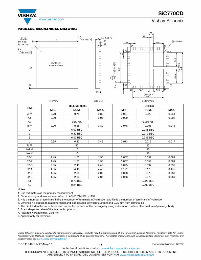
PACKAGE MECHANICAL DRAWING
Notes1. Use millimeters as the primary measurement2. Dimensioning and tolerances conform to ASME Y14.5M. - 19943. N is the number of terminals. Nd is the number of terminals in X-direction and Ne is the number of terminals in Y-direction4. Dimension b applies to plated terminal and is measured between 0.20 mm and 0.25 mm from terminal tip5. The pin #1 identifier must be existed on the top surface of the package by using indentation mark or other feature of package body6. Exact shape and size of this feature is optional7. Package warpage max. 0.08 mm8. Applied only for terminals
Vishay Siliconix maintains worldwide manufacturing capability. Products may be manufactured at one of several qualified locations. Reliability data for SiliconTechnology and Package Reliability represent a composite of all qualified locations. For related documents such as package/tape drawings, part marking, andreliability data, see www.vishay.com/ppg?62727.
DIM.MILLIMETERS INCHES
MIN. NOM. MAX. MIN. NOM. MAX.
A (8) 0.70 0.75 0.80 0.027 0.029 0.031
A1 0.00 - 0.05 0.000 - 0.002
A2 0.20 ref. 0.008 ref.
b (4) 0.20 0.25 0.30 0.078 0.098 0.011
D 6.00 BSC 0.236 BSC
e 0.50 BSC 0.019 BSC
E 6.00 BSC 0.236 BSC
L 0.35 0.40 0.45 0.013 0.015 0.017
N (3) 40 40
Nd (3) 10 10
Ne (3) 10 10
D2-1 1.45 1.50 1.55 0.057 0.059 0.061
D2-2 1.45 1.50 1.55 0.057 0.059 0.061
D2-3 2.35 2.40 2.45 0.095 0.094 0.096
E2-1 4.35 4.40 4.45 0.171 0.173 0.175
E2-2 1.95 2.00 2.05 0.076 0.078 0.080
E2-3 1.95 2.00 2.05 0.076 0.078 0.080
K1 0.73 BSC 0.028 BSC
K2 0.21 BSC 0.008 BSC
40
12 x
2 x
Pin 1 dotby marking
MLP66-40(6 mm x 6 mm)
10
1120
21
30
31
5 6
4
Top View Bottom ViewSide View
A
B
C
D
0.10 C B
E
0.10 C A A 0.08 C
A1
A20.41
K2
K1
D2-1 Pin #1 dent
E2-
1
e
D2-3 D2-2
E2-
3E
2-2
(Nd-
1)X
e
ref
.
(Nd-1)X e ref.
0.10
M
C A
B

Package Informationwww.vishay.com Vishay Siliconix
Revision: 12-Jan-15 1 Document Number: 64846For technical questions, contact: [email protected]
THIS DOCUMENT IS SUBJECT TO CHANGE WITHOUT NOTICE. THE PRODUCTS DESCRIBED HEREIN AND THIS DOCUMENTARE SUBJECT TO SPECIFIC DISCLAIMERS, SET FORTH AT www.vishay.com/doc?91000
PowerPAK® MLP66-40 Case Outline
Notes1. Use millimeters as the primary measurement
2. Dimensioning and tolerances conform to ASME Y14.5M. - 1994
3. N is the number of terminals. Nd is the number of terminals in X-direction and Ne is the number of terminals in Y-direction
4. Dimension b applies to plated terminal and is measured between 0.20 mm and 0.25 mm from terminal tip
5. The pin #1 identifier must be existed on the top surface of the package by using indentation mark or other feature of package body
6. Exact shape and size of this feature is optional
7. Package warpage max. 0.08 mm
8. Applied only for terminals
DIM.MILLIMETERS INCHES
MIN. NOM. MAX. MIN. NOM. MAX.
A (8) 0.70 0.75 0.80 0.027 0.029 0.031
A1 0.00 - 0.05 0.000 - 0.002
A2 0.20 ref. 0.008 ref.
b (4) 0.20 0.25 0.30 0.078 0.098 0.011
D 6.00 BSC 0.236 BSC
e 0.50 BSC 0.019 BSC
E 6.00 BSC 0.236 BSC
L 0.35 0.40 0.45 0.013 0.015 0.017
N (3) 40 40
Nd (3) 10 10
Ne (3) 10 10
D2-1 1.45 1.50 1.55 0.057 0.059 0.061
D2-2 1.45 1.50 1.55 0.057 0.059 0.061
D2-3 2.35 2.40 2.45 0.095 0.094 0.096
E2-1 4.35 4.40 4.45 0.171 0.173 0.175
E2-2 1.95 2.00 2.05 0.076 0.078 0.080
E2-3 1.95 2.00 2.05 0.076 0.078 0.080
K1 0.73 BSC 0.028 BSC
K2 0.21 BSC 0.008 BSC
ECN: T14-0826-Rev. B, 12-Jan-15DWG: 5986
40
12 x
2 x
Pin 1 dotby marking
MLP66-40(6 mm x 6 mm)
10
1120
21
30
31
5 6
4
Top View Bottom ViewSide View
A
B
C
D
0.10 C B
E
0.10 C A A 0.08 C
A1
A20.41
K2
K1
D2-1
E2-
1
e
D2-3 D2-2
E2-
3E
2-2
(Nd-
1)X
e
ref
.
(Nd-1)X e ref.
0.10
M
C A
B
Legal Disclaimer Noticewww.vishay.com Vishay
Revision: 08-Feb-17 1 Document Number: 91000
DisclaimerALL PRODUCT, PRODUCT SPECIFICATIONS AND DATA ARE SUBJECT TO CHANGE WITHOUT NOTICE TO IMPROVE RELIABILITY, FUNCTION OR DESIGN OR OTHERWISE.
Vishay Intertechnology, Inc., its affiliates, agents, and employees, and all persons acting on its or their behalf (collectively, “Vishay”), disclaim any and all liability for any errors, inaccuracies or incompleteness contained in any datasheet or in any other disclosure relating to any product.
Vishay makes no warranty, representation or guarantee regarding the suitability of the products for any particular purpose or the continuing production of any product. To the maximum extent permitted by applicable law, Vishay disclaims (i) any and all liability arising out of the application or use of any product, (ii) any and all liability, including without limitation special, consequential or incidental damages, and (iii) any and all implied warranties, including warranties of fitness for particular purpose, non-infringement and merchantability.
Statements regarding the suitability of products for certain types of applications are based on Vishay’s knowledge of typical requirements that are often placed on Vishay products in generic applications. Such statements are not binding statements about the suitability of products for a particular application. It is the customer’s responsibility to validate that a particular product with the properties described in the product specification is suitable for use in a particular application. Parameters provided in datasheets and / or specifications may vary in different applications and performance may vary over time. All operating parameters, including typical parameters, must be validated for each customer application by the customer’s technical experts. Product specifications do not expand or otherwise modify Vishay’s terms and conditions of purchase, including but not limited to the warranty expressed therein.
Except as expressly indicated in writing, Vishay products are not designed for use in medical, life-saving, or life-sustaining applications or for any other application in which the failure of the Vishay product could result in personal injury or death. Customers using or selling Vishay products not expressly indicated for use in such applications do so at their own risk. Please contact authorized Vishay personnel to obtain written terms and conditions regarding products designed for such applications.
No license, express or implied, by estoppel or otherwise, to any intellectual property rights is granted by this document or by any conduct of Vishay. Product names and markings noted herein may be trademarks of their respective owners.
© 2017 VISHAY INTERTECHNOLOGY, INC. ALL RIGHTS RESERVED