DRM Class Project - University of Texas at...
24
DRM Class Project EE382V-SoC Fall 2009 Andreas Gerstlauer Mark McDermott The University of Texas at Austin EE 382V Class Notes Foil # 2 Project Description The class will be assigned to teams to do the various components of the design. The intent of the project is to do a HW/SW co-design of an embedded SOC. The design is a low power SOC implementation of the public domain DRM software implementation. We will use both a virtual platform (ARM) and a hardware platform (TLL5000-TLL6219) to simulate the design. These platforms consist of an ARM processor, I/O devices, memory components, hardware accelerators interconnected via a standard bus.
Transcript of DRM Class Project - University of Texas at...

DRM Class Project
EE382V-SoCFall 2009
Andreas Gerstlauer
Mark McDermott
The University of Texas at AustinEE 382V Class Notes Foil # 2
Project Description
The class will be assigned to teams to do the various components of the design. The intent of the project is to do a HW/SW co-design of an embedded SOC. The design is a low power SOC implementation of the public domain DRM software implementation. We will use both a virtual platform (ARM) and a hardware platform (TLL5000-TLL6219) to simulate the design.
These platforms consist of an ARM processor, I/O devices, memory components, hardware accelerators interconnected via a standard bus.

The University of Texas at AustinEE 382V Class Notes Foil # 3
Project Objectives and Activities
The objectives of the project are as follows:1. Implement the DRM C++ code on a ARM based platform while
meeting the performance, area and power metrics.
The project activities include: Optimize the DRM C++ software for fixed point operation
Profile the updated DRM C++ software implementation to determine performance bottlenecks
Convert time critical functions to pseudo ANSI-C/SystemC code. Synthesize C code to Verilog for gate level implementation
Partition the software into components which will run on the ARMprocessor and on the hardware accelerators
Co-simulate and co-verify the HW/SW implementation
Develop a high level power model of the system
The University of Texas at AustinEE 382V Class Notes Foil # 4
DRM PC Based System Architecture
DRM code is designed to run on a desktop computer

The University of Texas at AustinEE 382V Class Notes Foil # 5
DRM Software Overview
The University of Texas at AustinEE 382V Class Notes Foil # 6
DRM SW System Architecture

The University of Texas at AustinEE 382V Class Notes Foil # 7
High Level HW Architecture
FlashMemory
Buffer
ConfigurableLogic
(FPGA)
ARM-9EmbeddedProcessor
(iMX21)SDRAMMemory
SDRAMMemory
Ethernet
RS232
USB 1.1
TLL5000
TLL6219
The University of Texas at AustinEE 382V Class Notes Foil # 8
HW Development Tasks
Develop the following FPGA modules: Memory Controller
Interface to ARM Board and on chip bus
Hardware Accelerators (using Catapult code)
Clocking & Reset
Interrupt logic
Diagnostics

The University of Texas at AustinEE 382V Class Notes Foil # 9
Software based tasks
Compile FLP DRM and get it running on ARM board Profile code on ARM board
Convert FLP -> FXP in DRM code Run SNR checks
Modify conversion as needed
Compile FXP DRM and get it running on ARM board Profile code on ARM board
Develop streaming I/O handler
Develop interrupt handler
Develop HAL
TLL500 Prototyping Board

The University of Texas at AustinEE 382V Class Notes Foil # 11
TLL5000PrototypingPlatform
The University of Texas at AustinEE 382V Class Notes Foil # 12
USB
100Base-T
PS-2
RS232
AudioCodec
VGAOut
CompactFlash Port
FlashMemory
Mezzanine
Connectors
Video DAC
ARM-7 COP
USBJTAG
PowerControl
ConfigurableLogic
(FPGA)
SDRAMMemory
AudioOut
AudioIn
PowerConnector
EthernetPHY
USB2.0
PHY
DIP Switches
VideoIn/OutNTSC/PAL
Encoder/Decoder
7-SEG LED Bank
Buffers
Buffers
Mezzanine
Connectors
TLL 5000 Architecture

The University of Texas at AustinEE 382V Class Notes Foil # 13
Xilinx Spartan 3 FPGA
Spartan 3 XC3S1500 DiscussionOverview
Logic Resources
Memory Resources
Clock Resources
Input/Output Resources
The University of Texas at AustinEE 382V Class Notes Foil # 14
Spartan 3 Overview

The University of Texas at AustinEE 382V Class Notes Foil # 15
Interconnect Matrix
Channels contain various connection resources
The University of Texas at AustinEE 382V Class Notes Foil # 16
Channel Interconnects

The University of Texas at AustinEE 382V Class Notes Foil # 17
CLBs & Slices
• Each slice has 2 LUTs& 2 storage elements
The University of Texas at AustinEE 382V Class Notes Foil # 18
CLB Slice
• 2 FFs or latches
• 2 LUTs for combinational logic
• Some LUTs can be used as distributed RAM or ROM, or shift registers
• Carry look-ahead
• Dedicated muxes

The University of Texas at AustinEE 382V Class Notes Foil # 19
Multipliers
• 2’s-complement multipliers distributed across fabric
Primarily to support DSP Cascade connections
Pipeline registers on inputs and outputs
Can do 2 small width op• Can also be used for
Barrel shifters
Data storage• Some shared connections with
adjacent block RAM
The University of Texas at AustinEE 382V Class Notes Foil # 20
Block RAM

The University of Texas at AustinEE 382V Class Notes Foil # 21
Clock Network
The University of Texas at AustinEE 382V Class Notes Foil # 22
Digital Clock Manager (DCM)
DCM functionsEliminate clock skew using Delay-Locked Loop (DLL)
Monitors clock skew on output and corrects
Performs frequency doubling
Creates multiphase clocks
Fractional Digital Frequency Synthesizer (DFS)
fOUT = M/N fIN
Clock conditioning
Clock buffering and signal translation

The University of Texas at AustinEE 382V Class Notes Foil # 23
Digital Clock Manager (DCM)
The University of Texas at AustinEE 382V Class Notes Foil # 24
Input/Output Block (IOB)
• Slew rate and drive strength control
• Pull-up, pull-down and keeper
• DDR signals
• Controlled-Z input/output
• Boundary scan

The University of Texas at AustinEE 382V Class Notes Foil # 25
I/O Standards
TLL6219 ARM Processor Board

The University of Texas at AustinEE 382V Class Notes Foil # 27
TLL6219 ARM Processor Board
EthernetChip
i.MX21
Flash
SD
RA
M
SD
RA
M
CPLD
User Switch
FlashReset
RJ-45Ethernet
Connector
RJ-12Serial
Connector
MiniUSB
LCD connector
Boot ModeJumpers
User
LE
Ds
Power LED
20 Pin CPU JTAG
40 Pin
GP
IO co
nn
ector
PowerSupply
The University of Texas at AustinEE 382V Class Notes Foil # 28
Mezzanine Connectors
CPLD
ARM-9EmbeddedProcessor
(iMX21)
Ethernet
USB 1.1
DataBuffers
SDRAMMemory
Expansion Port
RS-232, GPIO
Flash Memory
Control
AddressBuffers
JTAGHeader
ControlJTAG DATA ADDRESS
DATA
ADDRESS
SW & LED
TLL6219 Block Diagram
RS232

The University of Texas at AustinEE 382V Class Notes Foil # 29
i.MX21 Features
The University of Texas at AustinEE 382V Class Notes Foil # 30
BlockDiagram

The University of Texas at AustinEE 382V Class Notes Foil # 31
iMX21 Memory Map
There are eight 512MB partitions
The University of Texas at AustinEE 382V Class Notes Foil # 32
iMX21 Memory MapDetails

The University of Texas at AustinEE 382V Class Notes Foil # 33
The University of Texas at AustinEE 382V Class Notes Foil # 34
TLL6219 ARM926EJ-S Board
External interfacesRS-232 serial port
Ethernet
USB-OTG (Linux host driver for flash disk)
Graphic LCD panel
TLL5000 InterfaceExternal memory interface
/CS1, /CS5 memory regions
D[31:0], A[23:0], control signals (thru CPLD)
Connections to TLL6219 CPLD

The University of Texas at AustinEE 382V Class Notes Foil # 35
Interface from ARM to FPGA
All access from the ARM9 to hardware will be through the Chip Select 1 & 5 memory regions
All TLL5000 peripherals must be accessed through the FPGA
The only direct connection to the ARM9 isQVGA LCD with touchscreen
RS-232
Ethernet
The University of Texas at AustinEE 382V Class Notes Foil # 36
System Block Diagram

The University of Texas at AustinEE 382V Class Notes Foil # 37
TLL6219 Mezzanine Connector A
The University of Texas at AustinEE 382V Class Notes Foil # 38
TLL6219 Mezzanine Connector B
The University of Texas at AustinEE 382V Class Notes Foil # 39
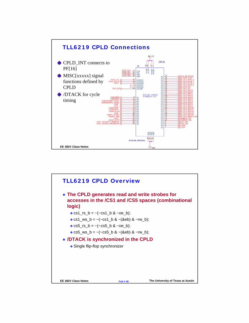
TLL6219 CPLD Connections
CPLD_INT connects to PF[16]
MISC[xxxxx] signal functions defined by CPLD
/DTACK for cycle timing
The University of Texas at AustinEE 382V Class Notes Foil # 40
TLL6219 CPLD Overview
The CPLD generates read and write strobes for accesses in the /CS1 and /CS5 spaces (combinational logic) cs1_rs_b = ~(~cs1_b & ~oe_b);
cs1_ws_b = ~(~cs1_b & ~(&eb) & ~rw_b);
cs5_rs_b = ~(~cs5_b & ~oe_b);
cs5_ws_b = ~(~cs5_b & ~(&eb) & ~rw_b);
/DTACK is synchronized in the CPLDSingle flip-flop synchronizer

The University of Texas at AustinEE 382V Class Notes Foil # 41
TLL6219 CPLD_MISC[] Pins
mz_cpld_misc[0] = cs1_rs_b; /CS1 read strobe (active-low)mz_cpld_misc[1] = cs1_ws_b; /CS1 write strobe (active-low)mz_cpld_misc[2] = cs5_rs_b; /CS5 read strobe (active-low)mz_cpld_misc[3] = cs5_ws_b; /CS5 write strobe (active-low)mz_cpld_misc[4] = oe_b; from ARM926mz_cpld_misc[5] = cs0_b; from ARM926 (flash memory)mz_cpld_misc[6] = cs1_b; from ARM926 (FPGA access)mz_cpld_misc[7] = cs2_b; from ARM926 (SDRAM)mz_cpld_misc[8] = cs3_b; from ARM926 (Ethernet)mz_cpld_misc[9] = cs5_b; from ARM926 (FPGA access)mz_cpld_misc[10] = nfio4; TLL6219 jumpermz_cpld_misc[11] = nfio5; TLL6219 jumpermz_cpld_misc[12] = data_dir; TLL6219 transceiver controlmz_cpld_misc[13] = data_oe; TLL6219 transceiver controlmz_cpld_misc[14] = fpga_interrupt; FPGA IRQ to ARM926 PF[16]
The University of Texas at AustinEE 382V Class Notes Foil # 42
TLL6219 Transceiver Control
The NFIO4 jumper is used to control data transceiver operation when the ARM926 is NOT accessing /CS1 or /CS5 space
If the jumper is NOT installed, the data transceivers are disabled
If the jumper IS installed, the data transceivers are enabled toward the FPGA to permit snooping bus activity that is not in the /CS1 or /CS5 spaces

The University of Texas at AustinEE 382V Class Notes Foil # 43
iMX21 External Interface Module (EIM)
The EIM permits very fine-grained control of the bus interfaceBus width
Timing of /CSx assertion/negation
Timing of /OE, /WE assertion/negation
Dead cycles between transfers
DTACK sensitivity and sampling
Byte enable behavior
Burst mode
The University of Texas at AustinEE 382V Class Notes Foil # 44
iMX21 EIM Timing Example

The University of Texas at AustinEE 382V Class Notes Foil # 45
iMX21BusTimingwithuMonSettings
The University of Texas at AustinEE 382V Class Notes Foil # 46
Chip Select configuration set uMon
Chip Select 1 & 5 Upper Register settings in uMonCS1U,CS5U = 0x00000480
DCT = 0, at least 2 HCLK before /DTACK checked
RWA = 0, R/W asserted when address valid
WSC = 4 wait states (minimum cycle = 6 HCLK)
EW = 1, level sensitive /DTACK

The University of Texas at AustinEE 382V Class Notes Foil # 47
Chip Select configuration set uMon
Chip Select 1 & 5 Lower Register settings in uMonCS1L,CS5L = 0x22220E01
WEA = 2, byte enables asserted 2 half-clocks after start of access
WEN = 2, byte enables negated 2 half-clocks before end of access
OEA, OEN = 2, similar for /OE on reads
CSA = 0, /CS asserted when write starts
CSN = 0, /CS negated when write ends
EBC = 1, byte enables during writes only
DSZ = 6, 32-bit bus width
CSEN = 1, /CS enabled
The University of Texas at AustinEE 382V Class Notes Foil # 48
TLL5000 Block Diagram