Driving High-Speed ADCs
23
Application Report SLAA416A – November 2009 – Revised September 2010 Driving High-Speed Analog-to-Digital Converters: Circuit Topologies and System-Level Parameters John Miller, Tyler Pate .......................................................................................... High-Speed Products ABSTRACT This application report discusses the performance-related aspects of passive and active interfaces at the analog input of high-speed pipeline analog-to-digital converters (ADC). The report simplifies the many possibilities into two main categories: passive and active interface circuits. The first section of the report gives an overview of equivalent models of buffered and unbuffered ADC input circuits, passive interfaces based on transformers, as well as an overview of the metrics used to gauge the ADC analog performance in addition to the entire mixed-signal chain. Passive interfaces are frequently the best choice when there is flexibility in the applied signal level and signal loss in the interface is a non-issue. While the noise and distortion contributions of passive interfaces can be negligible, the inherent frequency-dependent power loss, passband ripple, low frequency limitations (for example, ac coupling), and cost can limit the usefulness of these interfaces. The second section of the report covers interface circuits using high-speed operational amplifiers and fully-differential amplifiers. High-speed amplifiers can provide flexible, cost-effective solutions when the application demands gain, a flat passband with low ripple, dc level shifts, or a dc-coupled signal path. The second section covers amplifier-specific performance metrics, common circuit topologies for high-speed amplifiers, and some detailed performance models that can help pick the best amplifier to achieve the desired combined (that is, an amplifier + ADC) performance. Contents 1 Analog Input Topologies of High-Speed Pipeline ADCs ............................................................... 3 2 High-Speed Pipeline ADCs with Unbuffered Analog Inputs ........................................................... 3 3 Unbuffered Analog Input Drive Circuit Requirements .................................................................. 4 4 Buffered Analog Input Equivalent Circuit Model ........................................................................ 6 5 Buffered Analog Input: Drive Circuit Requirements .................................................................... 7 6 High-Speed A/D Performance Metrics ................................................................................... 7 7 Examples of Active Drive Circuit Topologies for High-Speed ADCs ............................................... 10 8 Amplifier Performance Metrics ........................................................................................... 10 9 Distortion .................................................................................................................... 16 10 High-Speed Amplifier Circuit Architectures ............................................................................ 18 11 THS770006 Driving ADS5493: Single-Ended Input .................................................................. 19 12 Dual Op Amp Active Driver Considerations ............................................................................ 20 13 IF Amplifier ................................................................................................................. 21 14 References ................................................................................................................. 22 List of Figures 1 Example of an Equivalent Model of an Unbuffered Analog Input .................................................... 3 2 Example of a Passive Single Transformer Drive Circuit for an Unbuffered Analog Input ......................... 4 3 Example of a Passive Dual Transformer Drive Circuit for an Unbuffered Analog Input ........................... 4 4 Differential Input Impedance vs Frequency for an Unbuffered Sample-and-Hold Input ........................... 5 5 Example of an Equivalent Model of a Buffered Analog Input ......................................................... 6 6 Example of a Passive Transformer Drive Circuit for a Buffered Analog Input ...................................... 7 7 Analog Input Response of the ADS5481/2/3 Family ................................................................... 8 8 ADS5483 SNR (in dBFS): Contour Plots with Sampling Frequency vs Signal Input Frequency ................. 9 1 SLAA416A – November 2009 – Revised September 2010 Driving High-Speed Analog-to-Digital Converters Submit Documentation Feedback Copyright © 2009–2010, Texas Instruments Incorporated
Transcript of Driving High-Speed ADCs

Application ReportSLAA416A–November 2009–Revised September 2010
Driving High-Speed Analog-to-Digital Converters: CircuitTopologies and System-Level Parameters
John Miller, Tyler Pate .......................................................................................... High-Speed Products
ABSTRACT
This application report discusses the performance-related aspects of passive and active interfaces at theanalog input of high-speed pipeline analog-to-digital converters (ADC). The report simplifies the manypossibilities into two main categories: passive and active interface circuits. The first section of the reportgives an overview of equivalent models of buffered and unbuffered ADC input circuits, passive interfacesbased on transformers, as well as an overview of the metrics used to gauge the ADC analog performancein addition to the entire mixed-signal chain. Passive interfaces are frequently the best choice when there isflexibility in the applied signal level and signal loss in the interface is a non-issue. While the noise anddistortion contributions of passive interfaces can be negligible, the inherent frequency-dependent powerloss, passband ripple, low frequency limitations (for example, ac coupling), and cost can limit theusefulness of these interfaces.
The second section of the report covers interface circuits using high-speed operational amplifiers andfully-differential amplifiers. High-speed amplifiers can provide flexible, cost-effective solutions when theapplication demands gain, a flat passband with low ripple, dc level shifts, or a dc-coupled signal path. Thesecond section covers amplifier-specific performance metrics, common circuit topologies for high-speedamplifiers, and some detailed performance models that can help pick the best amplifier to achieve thedesired combined (that is, an amplifier + ADC) performance.
Contents1 Analog Input Topologies of High-Speed Pipeline ADCs ............................................................... 32 High-Speed Pipeline ADCs with Unbuffered Analog Inputs ........................................................... 33 Unbuffered Analog Input Drive Circuit Requirements .................................................................. 44 Buffered Analog Input Equivalent Circuit Model ........................................................................ 65 Buffered Analog Input: Drive Circuit Requirements .................................................................... 76 High-Speed A/D Performance Metrics ................................................................................... 77 Examples of Active Drive Circuit Topologies for High-Speed ADCs ............................................... 108 Amplifier Performance Metrics ........................................................................................... 109 Distortion .................................................................................................................... 1610 High-Speed Amplifier Circuit Architectures ............................................................................ 1811 THS770006 Driving ADS5493: Single-Ended Input .................................................................. 1912 Dual Op Amp Active Driver Considerations ............................................................................ 2013 IF Amplifier ................................................................................................................. 2114 References ................................................................................................................. 22
List of Figures
1 Example of an Equivalent Model of an Unbuffered Analog Input .................................................... 3
2 Example of a Passive Single Transformer Drive Circuit for an Unbuffered Analog Input ......................... 4
3 Example of a Passive Dual Transformer Drive Circuit for an Unbuffered Analog Input ........................... 4
4 Differential Input Impedance vs Frequency for an Unbuffered Sample-and-Hold Input ........................... 5
5 Example of an Equivalent Model of a Buffered Analog Input ......................................................... 6
6 Example of a Passive Transformer Drive Circuit for a Buffered Analog Input ...................................... 7
7 Analog Input Response of the ADS5481/2/3 Family ................................................................... 8
8 ADS5483 SNR (in dBFS): Contour Plots with Sampling Frequency vs Signal Input Frequency................. 9
1SLAA416A–November 2009–Revised September 2010 Driving High-Speed Analog-to-Digital ConvertersSubmit Documentation Feedback
Copyright © 2009–2010, Texas Instruments Incorporated

www.ti.com
9 ADS6445 SFDR: Contour Plots with Sampling Frequency vs Input Signal Frequency ........................... 9
10 Input-Referred Op Amp Noise Model ................................................................................... 11
11 Input-Referred Noise for the OPA2695 ................................................................................. 12
12 General Model for a Band-Limited Driver Circuit for a High-Speed ADC .......................................... 12
13 Differential Noninverting Amplifier....................................................................................... 13
14 Noise Analysis Circuit..................................................................................................... 13
15 Relative Amplifier SNR vs Relative System SNR, Both with Respect to A/D SNR: (SNRAMP – SNRA/D) vs(SNRSYS – SNRA/D) ......................................................................................................... 16
16 Amplifier Distortion vs System Distortion, Both with Respect to A/D Distortion: (HDAMP – HDA/D) vs. (HDSYS
– HDA/D) ..................................................................................................................... 18
17 High-Speed ADC Driver Amplifier with Single-Ended to Differential Input Conversion .......................... 19
18 High-Speed, ADC Driver Amplifier with High-Impedance Inputs (Based on the OPA2695)..................... 20
19 High-Speed ADC Driver Amplifier (Based on the THS4509) ........................................................ 21
20 High-Speed A/D Driver Amplifier (Based on the THS9001) ......................................................... 21
2 Driving High-Speed Analog-to-Digital Converters SLAA416A–November 2009–Revised September 2010Submit Documentation Feedback
Copyright © 2009–2010, Texas Instruments Incorporated

INP
INM
25 W
25 W
RCR Filter
50 W
50 W
3.2 pF
C
1 pFpar2
C
1 pFpar2
L
3 nHpkg
L
3 nHpkg
C
2 pFbond
C
2 pFbond
R
200esr
W
R
200esr
W
C
0.8 pFpar1
SamplingSwitch
SamplingSwitch
SamplingCapacitor
SamplingCapacitor
R
15on
W
R
15on
W
R
10on
W
C
4.0 pFsamp
C
4.0 pFsamp
www.ti.com Analog Input Topologies of High-Speed Pipeline ADCs
1 Analog Input Topologies of High-Speed Pipeline ADCs
Today’s CMOS and bipolar high-speed, analog-to-digital converters (ADCs) usually have pipelinearchitectures, but can have different analog input circuit topologies. CMOS ADCs (for example, theADS55xx and ADS61xx series devices) have unbuffered inputs where the sample-and-hold circuitry isdirectly connected to the analog input pins. Bipolar ADCs (such as the ADS54xx series devices), on theother hand, usually have analog inputs that are isolated from the sample-and-hold circuitry by an internalamplifier. Both types of high-speed ADCs often have input bandwidths much greater than the maximumsampling frequency and are capable of undersampling narrowband input signals. The following sectionscover the equivalent input circuit models and major performance metrics for these types of high-speedADCs.
2 High-Speed Pipeline ADCs with Unbuffered Analog Inputs
The equivalent model of an analog input from the ADS6444 data sheet is shown in Figure 1 as anexample of an unbuffered input stage. The analog input consists of a switched-capacitor-based,differential, sample-and-hold (S/H) architecture. Note that the FET which serves as a sampling switch isthe only active device between the analog input pins and the sampling capacitor. This device controls thecharge flow from the analog input pins into the sampling capacitor. The RLC networks that contain theLpkg, Cbond,and Resr, are equivalent models of the package and bond-wire parasitics. The RCR filter sets theanalog bandwidth of the device. The FETs control the charge and discharge of the sampling capacitors.
Figure 1. Example of an Equivalent Model of an Unbuffered Analog Input
The differential input topology results in good ac performance for high input frequencies at high samplingrates. The input sampling circuit of the ADS6149 has a high, –3-dB bandwidth that extends up to 700 MHz(measured from the input pins to the sampled voltage).The INP and INM pins must be externally biasedaround a common-mode voltage that is available as a reference voltage on the ADC VCM pin. For afull-scale differential input, each input pin INP, INM pair must swing symmetrically between VCM ±VPEAK. Ingeneral, this architecture results in a full-scale, differential, peak-to-peak input swing of 4 x VPEAK, whereVPEAK is the peak voltage at either input pin. As an example, the ADS6149 has a differential full-scale inputvoltage of 2 VPP, which is the result of a peak swing of ±0.5 V (at INP, INM) about the 1.5-Vcommon-mode voltage.
3SLAA416A–November 2009–Revised September 2010 Driving High-Speed Analog-to-Digital ConvertersSubmit Documentation Feedback
Copyright © 2009–2010, Texas Instruments Incorporated

INP
INM
VCM1:1
5 W
25 W
25 W
5 W
0.1 Fm
0.1 Fm
TF_ADC
S0256-01
ADS6xxx
INP
INM
VCM1:1 1:1
5 W
50 W
50 W
50 W
50 W
5 W
0.1 Fm
0.1 Fm
ADS6xxx
Unbuffered Analog Input Drive Circuit Requirements www.ti.com
3 Unbuffered Analog Input Drive Circuit Requirements
For optimum performance, the analog inputs must be driven differentially. This improves thecommon-mode noise immunity and even-order harmonic rejection. A 5-Ω resistor in series with each inputpin is recommended to damp out ringing caused by the package parasitics. It is also necessary to presentlow impedance (<50 Ω) for the common-mode switching currents. For example, this is achieved by usingtwo resistors from each input terminated to the common-mode voltage (VCM), as shown in Figure 2.
Figure 2. Example of a Passive Single Transformer Drive Circuit for an Unbuffered Analog Input
At high input frequencies, the mismatch in the transformer parasitic capacitance (between the windings)results in degraded even-order harmonic performance. Connecting two identical RF transformersback-to-back helps minimize this mismatch, and good performance is obtained for high-frequency inputsignals. Figure 3 shows an example using two transformers (for example, a Coilcraft WBC1-1). Anadditional termination resistor pair (enclosed within the shaded box in Figure 3) may be required betweenthe two transformers to improve the balance between the P and M sides. The center point of thistermination must be connected to ground to ensure optimal balance.
Figure 3. Example of a Passive Dual Transformer Drive Circuit for an Unbuffered Analog Input
4 Driving High-Speed Analog-to-Digital Converters SLAA416A–November 2009–Revised September 2010Submit Documentation Feedback
Copyright © 2009–2010, Texas Instruments Incorporated

S(1
, 1)
Frequency (100 kHz to 500 MHz)
F2F1
F1Freq = 50 MHzS(1, 1) = 0.967 / –13.241Impedance = 62.211 – j421.739
F2Freq = 400 MHzS(1, 1) = 0.273 / –59.329Impedance = 58.132 – j29.510
0
100
200
300
400
500
600
700
800
900
1000
0 50 100 150 200 250 300 350 400 450 500
Ma
gn
itu
de
of
Zin
--W
f -- Input Frequency -- MHzI
F1
F1
Frequency = 50 MHz
Mag(Zin1) = 426.302
F2
F2
Frequency = 400 MHz
Mag(Zin1) = 65.193
www.ti.com Unbuffered Analog Input Drive Circuit Requirements
In addition to the preceding considerations for unbuffered ADC inputs, the drive circuit may also have toprovide:
1. Low insertion loss over the desired frequency range;2. Input impedance that is matched to the signal source; and3. Output impedance that matches the ADC input.
For all of these reasons, the ADC input impedance must be taken into account when designing the drivecircuit. Figure 4 (from the ADS6444 product data sheet) shows that the impedance (ZIN, lookingdifferentially into the ADC input pins) decreases at high input frequencies. A Smith chart representation ofthe differential input impedance shows that the input impedance is capacitive over the operating band andcan be approximated by a series R-C up to about 500 MHz.
Figure 4. Differential Input Impedance vs Frequency for an Unbuffered Sample-and-Hold Input
5SLAA416A–November 2009–Revised September 2010 Driving High-Speed Analog-to-Digital ConvertersSubmit Documentation Feedback
Copyright © 2009–2010, Texas Instruments Incorporated

1000 W
1000 W
10 W
10 W
VCM
3 pF
3 pF AGND
INP
INM
AVDD5
AVDD5
ADS548x
AGND
AGND
~ 2 nH Bond Wire
~ 2 nH Bond Wire
~ 200 fFPackage
~ 200 fFPackage
~ 200 fFBond Pad
~ 200 fFBond Pad
AnalogInputs
BipolarTransistor
Buffer
BipolarTransistor
Buffer
Track and Hold,
1 Stagest
Pipeline
Buffered Analog Input Equivalent Circuit Model www.ti.com
4 Buffered Analog Input Equivalent Circuit Model
The equivalent model of a buffered analog input is shown in Figure 5, taken from the ADS5483 devicedata sheet. The ADS5483 is a fast, 16-bit, bipolar ADC. When an analog signal is applied to the deviceinput pins, it first passes through high-performance bipolar buffers before it is sampled by thetrack-and-hold circuit. The buffer isolates the board circuitry external to the ADC from the samplingglitches caused by the track-and-hold within the ADC. The buffers also present high impedances to theanalog inputs that are relatively constant over the usable bandwidth, unlike devices with unbuffered inputs.The conversion process is initiated by the falling edge of the external input clock. At that instant, thedifferential input signal is captured by the input track-and-hold, and the input sample is convertedsequentially by a series of lower resolution stages, with the outputs combined in a digital correction logicblock. Both the rising and the falling clock edges are used to propagate the sample through the pipelineevery half clock cycle. For the 16-bit ADS5483, this process results in a data latency of 4.5 clock cycles,after which the output data are available as a 16-bit parallel word, coded in offset binary format.
Figure 5. Example of an Equivalent Model of a Buffered Analog Input
The input common-mode of a buffered device is frequently set through internal resistors connecting eachinput signal path to the common-mode reference VCM. In the example (Figure 5), this configurationresults in a differential dc input impedance of 2 kΩ. In contrast, unbuffered inputs frequently requireexternal biasing circuitry to provide the common-mode voltage.
For the example shown in Figure 5 based on the ADS5483, a full-scale differential input is represented byeach input pin swinging symmetrically between 3.1 V ±0.75 V. This range means that each input has amaximum signal swing of 1.5 VPP for a total differential input signal swing of 3 VPP. Note that otherconverters may have different values for the full-scale input swing and/or the input common-mode voltage.
6 Driving High-Speed Analog-to-Digital Converters SLAA416A–November 2009–Revised September 2010Submit Documentation Feedback
Copyright © 2009–2010, Texas Instruments Incorporated
R
500
W
Z
500
W
ADS548x
INP
INM
R
200 WAC SignalSource
n = 2:1
www.ti.com Buffered Analog Input: Drive Circuit Requirements
5 Buffered Analog Input: Drive Circuit Requirements
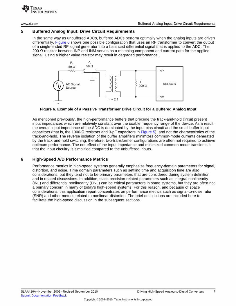
In the same way as unbuffered ADCs, buffered ADCs perform optimally when the analog inputs are drivendifferentially. Figure 6 shows one possible configuration that uses an RF transformer to convert the outputof a single-ended RF signal generator into a balanced differential signal that is applied to the ADC. The200-Ω resistor between INP and INM serves as a matching component and current path for the appliedsignal. Using a higher value resistor may result in degraded performance.
Figure 6. Example of a Passive Transformer Drive Circuit for a Buffered Analog Input
As mentioned previously, the high-performance buffers that precede the track-and-hold circuit presentinput impedances which are relatively constant over the usable frequency range of the device. As a result,the overall input impedance of the ADC is dominated by the input bias circuit and the small buffer inputcapacitors (that is, the 1000-Ω resistors and 3-pF capacitors in Figure 5), and not the characteristics of thetrack-and-hold. The reverse isolation of the buffer amplifiers minimizes common-mode currents generatedby the track-and-hold switching; therefore, two-transformer configurations are often not required to achieveoptimum performance. The net effect of the input impedance and minimized common-mode transients isthat the input circuitry is simplified compared to the unbuffered inputs.
6 High-Speed A/D Performance Metrics
Performance metrics in high-speed systems generally emphasize frequency-domain parameters for signal,distortion, and noise. Time domain parameters such as settling time and acquisition time are alsoconsiderations, but they tend not to be primary parameters that are considered during system definitionand in related discussions. In addition, static precision-related parameters such as integral nonlinearity(INL) and differential nonlinearity (DNL) can be critical parameters in some systems, but they are often nota primary concern in many of today's high-speed systems. For this reason, and because of spaceconsiderations, this application report concentrates on performance metrics such as signal-to-noise ratio(SNR) and other metrics related to nonlinear distortion. The brief descriptions are included here tofacilitate the high-speed discussion in the subsequent sections.
7SLAA416A–November 2009–Revised September 2010 Driving High-Speed Analog-to-Digital ConvertersSubmit Documentation Feedback
Copyright © 2009–2010, Texas Instruments Incorporated

f − Frequency − Hz
−24
−21
−18
−15
−12
−9
−6
−3
0
3
Norm
aliz
ed G
ain
−dB
10M 100M 1G
ADS5483
ADS5481
ADS5482
S10
N
PSNR = 10log
P
æ ö
ç ÷
è ø
High-Speed A/D Performance Metrics www.ti.com
Analog Bandwidth—Defined as the analog input frequency at which the power of the fundamental isreduced by 3 dB with respect to the low-frequency value. It also serves as a measure of the analog signalintegrity versus increasing frequency. High-speed data converters are frequently used in digital radioapplications to convert narrowband IF signals with carrier frequencies in the second or third Nyquist zoneswhere the input signal frequency is near or above the sampling frequency. If the signal chain has anappropriate degree of filtering, the signal does not alias onto itself, but an inadequate analog-to-digital(A/D) analog bandwidth degrades the desired signal, and possibly leads to degraded SNR and SFDR.Figure 7 (from the data sheet for the ADS5481/2/3 series of ADCs) illustrates the variability of the analogbandwidth within a product family.
Figure 7. Analog Input Response of the ADS5481/2/3 Family
Signal-to-Noise Ratio (SNR)—In high-speed ADC data sheets, SNR is expressed as the ratio of thepower of the fundamental (PS) input to the noise floor power (PN), excluding the power at dc and in the firstfive harmonics.
(1)
SNR is either given in units of dBc (dB relative to the carrier) or dBFS (dB relative to the A/D full-scale). IndBc units, the total measured noise is expressed relative to the measured carrier level. In dBFS units, themeasured noise is expressed as relative to the A/D full-scale level, but the measurement is usuallyexecuted with a carrier level –1 dB below the A/D full scale (for example, –1 dBFS). SNR expressed indBFS units is frequently used when defining system requirements because it represents a maximumnoise-limited dynamic range; or alternatively, the effective noise floor of the converter device.
See Figure 8 for a contour plot of the ADS5483 SNR with input frequency and sampling frequency as theplotting variables. The plot shows that the best SNR performance occurs when input frequencies are inthe first Nyquist zone, and that SNR degrades by only 3 dB when the input frequency moves to the thirdNyquist zone, which matches the behavior shown in Figure 7 of analog bandwidth.
8 Driving High-Speed Analog-to-Digital Converters SLAA416A–November 2009–Revised September 2010Submit Documentation Feedback
Copyright © 2009–2010, Texas Instruments Incorporated

10 50 100 150
f - Input Frequency - MHzIN
f-
Sam
plin
g F
req
uen
cy -
MS
PS
S
SNR - dBFS
200 250 30040
50
60
110
70
80
90
100
120
130
135
70 72 7473 75 76
78
78
78
77
77
77
79
79
78.5
78.5
78.5
71 80
76
76
76
75
75
75
74
7473
72
74
77 78 79
10 50 100 150
f - Input Frequency - MHzIN
f-
Sam
plin
g F
req
uen
cy -
MS
PS
S
SFDR - dBc
200 250 300 400 450350 50030
40
50
100
60
70
80
90
110
120
125
65 70 8075 85 90
8383
83
86
86
86
86
83
80
80
80
80
77
77
77
74
74
74 71
71
71
68
68
68
65
65
65
86
83
83
89
89
89
89
92
8086
www.ti.com High-Speed A/D Performance Metrics
Figure 8. ADS5483 SNR (in dBFS): Contour Plots with Sampling Frequency vs Signal Input Frequency
Spurious-Free Dynamic Range (SFDR)—The ratio of the power of the fundamental to the highest otherspectral component (either spur or harmonic). SFDR is typically given in units of dBc (dB to carrier). Acontour plot of SFDR versus input frequency and sampling frequency as the plotting variables is shown inFigure 9 (taken from the ADS6445 data sheet).
Figure 9. ADS6445 SFDR: Contour Plots with Sampling Frequency vs Input Signal Frequency
9SLAA416A–November 2009–Revised September 2010 Driving High-Speed Analog-to-Digital ConvertersSubmit Documentation Feedback
Copyright © 2009–2010, Texas Instruments Incorporated

SS3dB
0.35=
-
t¦
( )
( )( )
OUT OUT
MAXMAX MAX
MAX
V dV dSR = = Asin 2 t +
t dt dt
= 2 Acos 2 t +
Dæ ö æ ö æ öé ùÞ p¦ qç ÷ ç ÷ ç ÷ë û
D è øè ø è ø
p¦ p¦ q
Examples of Active Drive Circuit Topologies for High-Speed ADCs www.ti.com
Third-Order Intermodulation Distortion (IMD3)—IMD3 is the ratio of the power of the fundamental (atfrequencies f1 and f2) to the power of the worst spectral component at either frequency 2f1– f2 or 2f2– f1.IMD3 is either given in units of dBc (dB to carrier) when the absolute power of the fundamental is used asthe reference, or dBFS (dB relative to full-scale) when the power of the fundamental is extrapolated to thefull-scale range of the converter.
7 Examples of Active Drive Circuit Topologies for High-Speed ADCs
Many times, a driver amplifier is required to meet the signal chain requirements. These factors include, butare not limited to:
• Gain• DC-coupled signal path.• Buffering of the signal source• Conversion of a single-ended signal path to a differential signal path• Level shift
If a driver amplifier is needed, its parameters can have a major impact on the overall performance of thesystem formed by the amplifier and the converter. The next section describes major amplifier metrics andhow they affect the overall amplifier/converter performance. Subsequent sections describe various circuitarchitectures as well as other design and performance considerations.
8 Amplifier Performance Metrics
Small-Signal Bandwidth
Small-signal bandwidth is a measure of the ability of a device to act as a linear gain element over adefined frequency span. It is implicitly assumed that the signal level is small enough that its presence doesnot change the operating point of the amplifier; this metric also serves as the noise bandwidth of theamplifier. It is related to the small-signal rise and fall times via the relationship expressed in Equation 2:
(2)
where f–3dB is the –3dB small-signal bandwidth.
Slew Rate/Large-Signal Bandwidth
Slew rate is defined as the maximum ΔVOUT/Δt for a specified gain, output level, and RLOAD. As alarge-signal parameter, it represents the maximum possible speed of the device as it moves through itsdynamic range. Slew rate measurements are frequently done by measuring the rising and falling edges ofa large-signal pulse waveform. In these cases, the measurement range for ΔVOUT is the voltage deflectionthat covers 10% to 90% of the rising edge of the output waveform (or 90% to 10% of the falling edge).Slew rate is a large-signal parameter, and is unrelated to small-signal rise and fall times. Slew rate limitingis distortion caused by transitions of the input signal that are too fast for the amplifier output to track.Recall that during normal operation, an op amp acts as a closed-loop device that feeds back some of theoutput signal in an attempt to minimize an error signal. When the amplifier is slew-limited, the amplifieroutput can no longer track the input signal. Consequently, the feedback mechanism breaks down, which inturn allows the error signal to increase along with a subsequent increase in signal distortion. For all intentsand purposes, the slew-limited device is operating as an open-loop amplifier with degraded distortionperformance.
For the limiting case of a sinusoidal signal, VOUT = Acos(2pƒt + q) , the slew rate can be expressed interms of the large-signal bandwidth through the following relationships:
(3)
10 Driving High-Speed Analog-to-Digital Converters SLAA416A–November 2009–Revised September 2010Submit Documentation Feedback
Copyright © 2009–2010, Texas Instruments Incorporated

( )
3dB
O,Peak
=
3dBt=0
V = A 2
3dB
ASR = 2 Acos 2 t + θ 2
2
ASR = 2
2
-¦ ¦
-
-
p¦ p¦ p¦
p¦
Þ
+VS
–VS
Idealop amp
ini
inn
en
www.ti.com Amplifier Performance Metrics
If the input sinusoid frequency increases while holding the input peak amplitude constant, the slew rate ismaximized when the frequency equals the large-signal bandwidth, which corresponds to a 3-dB decreasein the output signal (that is, ƒ = ƒ–3dB, VO,Peak = A/√2). The slew rate is related to the –3-dB large-signalbandwidth as shown in Equation 4:
(4)
Where:ƒ–3dB = amplifier –3-dB large-signal bandwidth (BW)A = peak output before slew limiting
As a first-order approximation, the highest frequency in the desired signal should be five times less thanthe large-signal BW of the amplifier if distortion is to be minimized.
Noise/SNR
Signal-to-noise ratio was defined and discussed in an earlier section as the noise-related performancemetric for ADCs. However, the noise performance of high-speed amplifiers is usually expressed in theproduct data sheet in terms of the quantities shown in Figure 10. Ini and Inn represent the equivalentcurrent noise of the inverting input and noninverting input, respectively. An ideal operational amplifier (opamp) has no noise or current flow through the input terminals, so the current noise represents thenon-ideality and the uncertainty of the actual op amp inputs. These noise parameters are usuallyexpressed in high-speed op amp data sheets as current spectral densities, with the units typically inpA/Hz1/2 for a high-speed op amp with NPN or PNP input transistors, or fA/Hz1/2 for FET-input devices. Ifthe high-speed op amp is a voltage-feedback amplifier, then Ini ≈ Inn, and the device data sheet has asingle entry for current noise. If the device is a current-feedback amplifier, then as a rule, Ini > Inn and thedevice data sheet shows the noise currents with separate entries. The quantity en is an input-referredvoltage noise spectral density, and its units are usually nV/Hz1/2 for a high-speed op amp. Additionalinformation on high-speed, op amp noise performance and modeling may be found in application reportsSLVA043 and SBOA066, both available for download from the TI web site.
Figure 10. Input-Referred Op Amp Noise Model
11SLAA416A–November 2009–Revised September 2010 Driving High-Speed Analog-to-Digital ConvertersSubmit Documentation Feedback
Copyright © 2009–2010, Texas Instruments Incorporated
100
10
1
Frequency (Hz)
103
104
105
106
107
108
Curr
ent N
ois
e (
pA
/)
ÖH
z
Hz
Voltage N
ois
e (
nV
/)
Ö
Noninverting Input Current Noise
Inverting Input Current Noise
19pA/ÖHz
22pA/ÖHz
Input Voltage Noise 1.7nV/ÖHz
or FDA
CM
InterfaceFilter
AIN+
AIN–
HS A/D
Dualop amp
Amplifier Performance Metrics www.ti.com
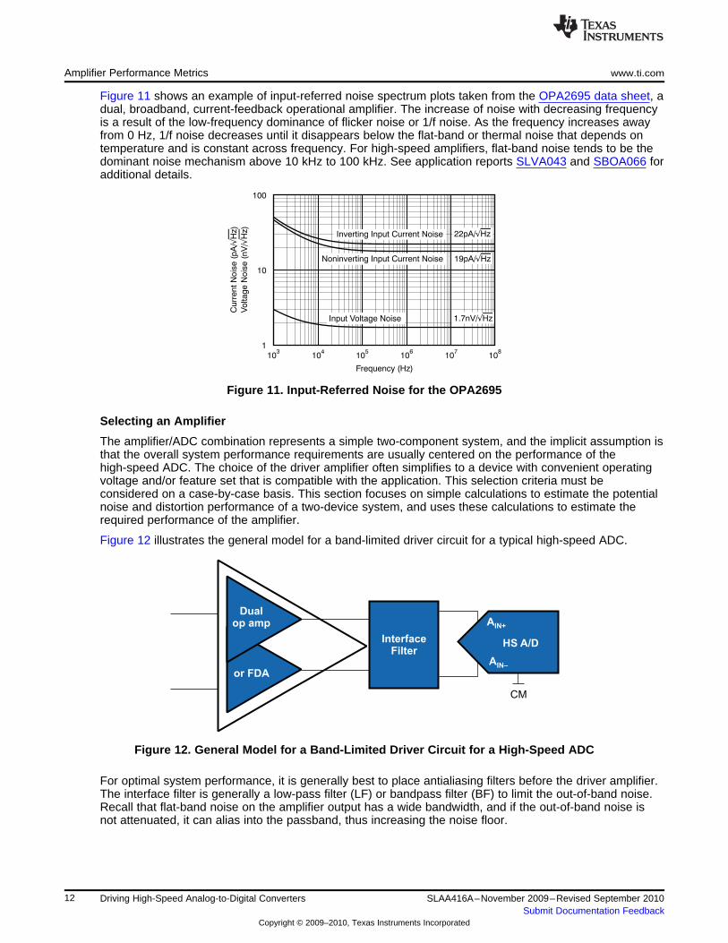
Figure 11 shows an example of input-referred noise spectrum plots taken from the OPA2695 data sheet, adual, broadband, current-feedback operational amplifier. The increase of noise with decreasing frequencyis a result of the low-frequency dominance of flicker noise or 1/f noise. As the frequency increases awayfrom 0 Hz, 1/f noise decreases until it disappears below the flat-band or thermal noise that depends ontemperature and is constant across frequency. For high-speed amplifiers, flat-band noise tends to be thedominant noise mechanism above 10 kHz to 100 kHz. See application reports SLVA043 and SBOA066 foradditional details.
Figure 11. Input-Referred Noise for the OPA2695
Selecting an Amplifier
The amplifier/ADC combination represents a simple two-component system, and the implicit assumption isthat the overall system performance requirements are usually centered on the performance of thehigh-speed ADC. The choice of the driver amplifier often simplifies to a device with convenient operatingvoltage and/or feature set that is compatible with the application. This selection criteria must beconsidered on a case-by-case basis. This section focuses on simple calculations to estimate the potentialnoise and distortion performance of a two-device system, and uses these calculations to estimate therequired performance of the amplifier.
Figure 12 illustrates the general model for a band-limited driver circuit for a typical high-speed ADC.
Figure 12. General Model for a Band-Limited Driver Circuit for a High-Speed ADC
For optimal system performance, it is generally best to place antialiasing filters before the driver amplifier.The interface filter is generally a low-pass filter (LF) or bandpass filter (BF) to limit the out-of-band noise.Recall that flat-band noise on the amplifier output has a wide bandwidth, and if the out-of-band noise isnot attenuated, it can alias into the passband, thus increasing the noise floor.
12 Driving High-Speed Analog-to-Digital Converters SLAA416A–November 2009–Revised September 2010Submit Documentation Feedback
Copyright © 2009–2010, Texas Instruments Incorporated

OPA2695
OPA2695
57.6 W
RG
35 W
402 W
R +5 VF
100 W
RO
12 pF
RS
RS
RO
35 W
100 W
VSIG V
OUT
RG
402 W
R –5 VF
57.6 W
Idealop amp
57.6 W 402 We
n,RG en,RF
en,Ro
100 W
24 pF VOUT
/2
+
–Noise Circuit
Output
ini
inn
en,RS
RS
en
VSIG
/2
www.ti.com Amplifier Performance Metrics
Noise
The following discussion gives an example of a noise analysis for a common circuit architecture used as ahigh-speed ADC driver. Figure 13 shows a differential noninverting amplifier similarly based on theOPA2695, a dual current-feedback device with a symmetrical pinout optimized to serve as an A/D driver.The amplifier/ADC interface filter is formed by the 100-Ω output resistors and the 12-pF capacitor actingas a differential LF with a –3-dB corner frequency of 66 MHz. The function of the LF is to attenuate thehigh-frequency noise that falls out of the usable band. The equivalent noise bandwidth of a single-pole RCfilter is (p/2)f–3dB. This value can be interpreted as the cutoff frequency of an ideal brick-wall filter. Ifpassband flatness is critical, then the –3-dB corner of a single-pole RC filter must be 6.5 times greaterthan the highest signal frequency. In this example, the recommended passband is f <10 MHz. Foradditional information on filter design for ADC driver circuits, see application reports SLWA053 andSBAA108.
Figure 13. Differential Noninverting Amplifier
For the purposes of noise analysis, the circuit can be split into two single-ended amplifiers, with the SNRperformance of either half being representative of the entire circuit (see Figure 14). Figure 14 shows theamplifier input-referred noise sources described earlier (Inn, Ini, and en) as well as the equivalent noisesources arising from the external resistors (en,RG, en,RF, en,Ro, and en,RS).
Figure 14. Noise Analysis Circuit
13SLAA416A–November 2009–Revised September 2010 Driving High-Speed Analog-to-Digital ConvertersSubmit Documentation Feedback
Copyright © 2009–2010, Texas Instruments Incorporated

( )nn S F Gi R 1 R R+
ni Fi R
( )N F Ge 1 + R R
G4kTR F GR 4kT R
F4kTR F4kTR
S4kTR ( )S F G4kTR 1 + R R
( )2o,nOUT,Amp,
n
2 2 2 2 2 2
e = e
= 5.3 + 8.8 + 13.6 + 6.7 + 2.54 + 6
= 19.4 nV Hz
± å
2 2 2OUT,Amp OUT,Amp,(+) OUT,Amp,( ) OUT,Amp
2OUT,Amp
e = e + e = 2e
= e 2
= 27.4 nV Hz
-
Amplifier Performance Metrics www.ti.com
Many high-speed applications require an operating bandwidth that is much greater than the op amp 1/fnoise bandwidth. Because of this requirement, low-frequency 1/f noise often has a negligible impact onthe overall noise performance of the circuit. For example, Figure 11 shows the OPA2695 noise isdominated by flat-band noise for f > 10 kHz (that is, the device 1/f noise is negligible for f > 10 kHz); so,for operating bandwidths greater than 1 MHz, ignore the effects of 1/f noise, which results in an error ofless than 6%. This device is intended to operate at frequencies well above 1 MHz; therefore, this error willbe negligible. Table 1 summarizes the op amp flat-band noise sources and their individual contributions tothe circuit output noise spectrum.
Table 1. Op Amp Flat-Band Noise Sources and Contributions to Typical Circuit Output NoiseSpectrum
Noise Output NoiseNoise Source Value Noise Source Origin Output Noise ExpressionSource Spectrum, eo,n
Inn 19 nV/Hz1/2 5.3 nV/Hz1/2
Ini 22 pA/Hz1/2 8.8 nV/Hz1/2OPA2695 data sheet
en 1.7 nV/Hz1/2 13.6 nV/Hz1/2
en,RG 0.96 nV/Hz1/2 6.7 nV/Hz1/2
en,RF 2.54 nV/Hz1/2 2.54 nV/Hz1/2
en,RS 0.75 nV/Hz1/2 6 nV/Hz1/2
Where k is Boltzmann’s constant (1.381 × 10⁻²³ J/K) and T is the temperature in Kelvins (290°K for thisanalysis). For additional background and details on high-speed operational amplifier noise analysis, seeapplication reports SLVA043 and SBOA066.
Because the individual noise sources are statistically independent from and uncorrelated with one another,the total output spectrum of our noise analysis circuit may be calculated as a sum-of-squares:
(5)
Which is the equivalent flat-band output noise spectrum of this single-ended analysis circuit. The noise inthis single-ended circuit is equal to and uncorrelated from any noise in the other single-ended circuit thatforms the other half of this differential amplifier. So, the total noise of the entire differential circuit is thesum-of-squares of the two individual noise terms:
(6)
14 Driving High-Speed Analog-to-Digital Converters SLAA416A–November 2009–Revised September 2010Submit Documentation Feedback
Copyright © 2009–2010, Texas Instruments Incorporated

( )2 2Amp,Filter N OUT,Amp n,Ro
6 2OUT,Amp rms
e = BW e + e
= 104 10 e + 4kT(100) = 280 V
´
é ù´ ´ më û
( )
( )
2o
Amp/Filter 2 2OUT,Filter
2/ 2 2VSNR = 10log = 20log = 69.5 dB
e 280 V
æ öæ ö
ç ÷ç ÷
ç ÷ç ÷ç ÷mè øè ø
2 2 2Total Amp/Filter ADCe = e + e
22 2Amp/FilterTotal ADC
2 2 2FS FS FS
ee e= +
V V V
( )2 2nSNR = 10log V e
1 1 1System Amp/Filter ADCSNR = SNR + SNR- - -
( )Amp/Filte ADCSNR 10 SNR 10
SystemSNR = 10log 10 + 10- -
-
www.ti.com Amplifier Performance Metrics
Following from the earlier assumption of dominant flat-band noise, it can be assumed that the outputspectrum is constant over the passband of the op amp, and only the output low-pass filter limits thebandwidth of the amplifier output noise. The 66-MHz, single-pole, low-pass filter has an equivalent noisebandwidth of (p/2) × f–3dB = 1.57 × 66 MHz = 104 MHz (see SLVA043), which allows the calculation of anequivalent filter output noise voltage over the passband.
(7)
If the nominal signal out of the low-pass filter is a 2-VPP sinusoid, then the available SNR for the entiredifferential amplifier/filter circuit is:
(8)
Note that halving the op amp gain (doubling RG) increases the output SNR by 3.5 dB, whereas halving thelow-pass filter f–3dB corner frequency (to 33 MHz) increases the SNR by 3 dB. The output SNR matchesany change in the input level decibel for decibel.
Because the amplifier and ADC noise mechanisms are independent, it is reasonable to assume that thenoise terms for the two devices are additive in a sum-of-squares sense; the total noise can then beexpressed as:
(9)
Recalling that the major noise-related ADC parameter is SNR referenced to the ADC full-scale inputvoltage, the total noise can be expressed as:
(10)
Where VFS is the ADC full-scale input voltage. Recalling that , the maximum totalSNR can be expressed as:
(11)
In Equation 11, SNR is in linear units, not dB. If the quantities are in dB units, the expression becomes:
(12)
One key result from Equation 12 is that an active ADC driver always contributes noise to the signal path,and the overall system SNRSystem is always less than SNRADC.
15SLAA416A–November 2009–Revised September 2010 Driving High-Speed Analog-to-Digital ConvertersSubmit Documentation Feedback
Copyright © 2009–2010, Texas Instruments Incorporated

( ) ( ) ( )
( ) ( )
dBx 10
dB Amp/Filter ADC 10dBdB
dB System ADC dBdB
Δ = SNR SNR = 10log 10 1
where:
x = SNR SNR 0 dB
-- - -
- £
-10
-5
0
5
10
15
20
-10 -9 -8 -7 -6 -5 -4 -3 -2 -1 0
X : System SNR w/respect to ADC SNR - dBdb
Dd
b:
Am
p S
NR
w/r
esp
ect
toA
DC
SN
R -
dB
2
1
3
Amplifier SNR Versus to System SNR
Both Axes are Expressed Relative to the ADC SNR
ADC noise is
dominant
Amp/filter noise is
dominant
Distortion www.ti.com
Many times, the ADC noise performance drives the noise requirements of the rest of the signal chain. Withthat practice in mind, it can be useful to specify the relative difference between the system and ADCSNRs, so that one can then calculate how much larger the amplifier SNR needs to be than the ADC SNRto support the system noise requirement. In other words, if you can specify xdB = (SNRSystem)dB –(SNRADC)dB, then it is possible to calculate Δ dB = (SNRAmp/Filter)dB – (SNRADC)dB via the followingrelationship:
(13)
Figure 15 provides an easy way to estimate the required amplifier SNR rise above the ADC (ΔdB) toachieve the total system SNR degradation with respect to the ADC (xdB).
The numbered points on the curve represent some specific cases of amplifier and ADC noise.
1. ΔdB = 0 dB: the amplifier/filter and ADC have the same SNR: SNRAmp,Filter = SNRADC = SNR, then thesystem SNR is 3 dB less than either → SNRSystem = SNRdB – 3 dB.
2. xdB = –1 dB: the system SNR can be 1 dB less than SNRADC → SNRSystem = SNRADC – 1 dB. → Δ dB =5.9 dB: The amplifier/filter must have an SNR that is 5.9 dB greater than the ADC
3. If SNRSystem to be 0.1 dB less than SNRADC → SNRSystem = SNRADC – 0.1 dB, → Δ dB = 16.3 dB: Theamplifier/filter must have an SNR that is 16.3 dB greater than the ADC.
Figure 15. Relative Amplifier SNR vs Relative System SNR,Both with Respect to A/D SNR: (SNRAMP – SNRA/D) vs (SNRSYS – SNRA/D)
9 Distortion
This section presents a simple set of calculations that can help model the total distortion of this simpleamplifier/ADC system. A complete and thorough discussion of distortion behavior for amplifiers and forADCs is available from other sources such as the Analog Applications Journal (see article SLYT133, forexample). The goal of this section is similar to what was presented in the amplifier/ADC noise calculationssection: to focus on a method that allows a designer to pick an op amp based on the overall performancerequirements. The analysis of the combined harmonic distortion for the amplifier and ADC is similar to the
16 Driving High-Speed Analog-to-Digital Converters SLAA416A–November 2009–Revised September 2010Submit Documentation Feedback
Copyright © 2009–2010, Texas Instruments Incorporated

HD,Total HD,Amp/Filter HD,ADCv = v + v
HD,Amp/FilterHD,Total HD,ADC
FS FS FS Total Amp/Filter ADC
vv v 1 1 1= + = +
V V V HD HD HDÞ
( )Amp/Filte ADCHD 20 HD 20
SystemHD = 20log 10 + 10
( ) ( ) ( )
( ) ( )
dBy 20HD,dB Amp/Filter ADC 10dBdB
dB System ADC dBdB
Δ = HD HD = 20log 10 1
where:
y = HD HD 0 dB
- -
- ³
www.ti.com Distortion
SNR analysis previously shown. One important difference is that amplifier distortion products and ADCdistortion products are correlated with one another, unlike the noise terms in the previous analysis. Theresult of this condition is that the analysis is restricted to a worst-case assumption that individual amplifierdistortion components and individual ADC distortion components sum as voltages rather than as powers(sum-of-squares done in the previous noise analysis).
Many times, ADC distortion is specified in terms of the spurious-free dynamic range (SFDR), theworst-case spur relative to the full-scale voltage, which may not be harmonically related to the desiredsignal. Amplifier distortion, on the other hand, is usually specified via HD2, HD3, and/or IMD2/3, which areall harmonically related to the desired signal.
The output of the amplifier/filter contains a desired signal component, as well as HD2 and HD3components. When the desired signal is applied to the ADC input, it generates its own harmonic distortionthat sums constructively or destructively with the HD2 and HD3 from the amplifier/filter. As previouslydiscussed, the worst-case scenario occurs when each of the amplifier and the ADC distortion componentssum constructively as voltages:
(14)
If the voltages are referenced to the ADC full-scale voltage and the signal is a simple sinusoid (carrier),the expression becomes:
(15)
Where no distinction has yet been made between HD2 or HD3, and the quantities in the second row of theequation are linear and have no units. Note that HD in this case refers to a single harmonic spur—such asHD2 or HD3—and not the composite total harmonic distortion (THD).
(16)
In a manner similar to the previous noise analysis, an expression can be developed which gives theamplifier HD performance (relative to the ADC) that results from a required, overall system HD (alsorelative to the ADC):
(17)
17SLAA416A–November 2009–Revised September 2010 Driving High-Speed Analog-to-Digital ConvertersSubmit Documentation Feedback
Copyright © 2009–2010, Texas Instruments Incorporated

-30
-25
-20
-15
-10
-5
0
5
10
0 1 2 3 4 5 6 7 8 9 10 11 12 13X : System HD w/respect to ADC HD - dBcdb
D:
Am
p H
D w
/resp
ect
toA
DC
HD
- d
Bc
HD
,db
Amplifier Distortion Versus System Distortion
Both Axes are Expressed Relative to the ADC HD
2
1
3
ADC distortion
is dominant
Amp/filter distortion
is dominant
High-Speed Amplifier Circuit Architectures www.ti.com
Figure 16 provides an easy way to estimate the required amplifier HD rise above the ADC (ΔHD,dB) toachieve the total system HD degradation with respect to the ADC (ydB).
The numbered points on the curve represent some specific cases of amplifier and ADC noise.
1. ΔHD,dB = 0 dB: the amplifier/filter and ADC have the same HD and HDAmp,Filter = HDADC = HD, and thesystem HD is 6 dB greater than either → HDSystem = HDdB + 6 dB.
2. xdB = 3 dB: the system HD can be 3 dB worse than HDADC so HDSystem = HDADC + 3 dB and ΔHDdB =–7.7 dB. The conclusion: the amplifier/filter must have an HD that is 7.7 dB better than the ADC.
3. If HDSystem to be 1 dB worse than HDADC → HDSystem = HDADC + 1 dB,→ ΔHD,dB = –18.3 dB: The amplifier/filter must have an HD that is 18.3 dB better than the ADC.
Figure 16. Amplifier Distortion vs System Distortion,Both with Respect to A/D Distortion: (HDAMP – HDA/D) vs. (HDSYS – HDA/D)
Note that many board-related factors can specifically affect HD2 and have little impact on HD3. Thesefactors include power supply bypassing as well as mechanical and electrical symmetry of the layout. If adifferential signal path is unsymmetrical in terms of component values and/or signal path routing, then itsability of the differential signal path to provide the natural attenuation of HD2 can be compromised. Foradditional information on best practices for high-speed PC board layouts, see application report SBAA113.
10 High-Speed Amplifier Circuit Architectures
This section provides application examples based on two ADCs, the ADS5493 and the ADS6444. TheADS5493 is a 130-MSPS, fully-differential ADC that has low-noise performance and outstanding SFDRover a wide frequency range. The ADS5493 is naturally coupled with the THS770006, a fixed-gain (+6dB), 14-/16-bit, fully-differential, wideband op amp to provide a complete signal conditioning and dataacquisition solution for high-speed applications. Interfacing the two devices with an application-specificfilter allows the designer to maintain the high-performance, low-distortion characteristics desired in signalconversion.
18 Driving High-Speed Analog-to-Digital Converters SLAA416A–November 2009–Revised September 2010Submit Documentation Feedback
Copyright © 2009–2010, Texas Instruments Incorporated

50 W50 W
Z
1:1
50 W
50 W
.1 Fm
RS
RS
RF
RF
200 W
200 W
5 pF
.1 Fm
.1 Fm
THS770006
ADS5493
www.ti.com THS770006 Driving ADS5493: Single-Ended Input
The ADS6444 is a quad, 125-MHz, CMOS ADC that can be driven by a variety of op amp driversdepending on application and performance needs. The specific examples discussed here are taken from aprototype evaluation board that contains three active driver circuits and a single transformer-coupledpassive signal path. The evaluation board features the ADS6444. The three active drivers were chosen forthis EVM to provide an array of driver solutions that can operate effectively over the first three Nyquistzones of the ADC. The circuits are based on the following devices and functionality with the ADS6444:
1. OPA2695: Dual current-feedback op amp that can be easily configured as a high-gain, fastinstrumentation amplifier. It can provide 14-bit noise and distortion performance through the firstNyquist zone.
2. THS4509: Fast fully-differential amplifier (FDA) that can provide excellent dynamic range for abroadband signal through the first Nyquist zone of the ADS6444, and in the second Nyquist zone withappropriate band-pass filtering.
3. THS9001: IF/RF amplifier which can serve as an effective ADC driver for high-IF narrowband signalssuch as those generally found in digital radio signal chains.
11 THS770006 Driving ADS5493: Single-Ended Input
Figure 17 shows a configuration that uses a transformer to convert from a single-ended input tofully-differential signaling, as is the default configuration on the ADS5493EVM. The ADS5493EVM has anonboard analog signal path with room for the THS770006 as well as a generic filter network layout thatenables rapid prototyping for target frequency ranges. To ensure there are no offsets in the amplifieroutput, both amplifier inputs should be impedance- and bias-matched. In this example, the two 50-Ωresistors in front of the THS770006 provide termination-matching for the input transmission line before thetransformer, assuming a turns ratio of 1:1.
Note: This document refers to the ADS5493EVM prototype; changes may be made in the releasedversion of the EVM.
The gain of the THS770006 is set at +6 dB by the internal feedback resistor network, RF and RS. Theoutput stage of the amplifier drives a filter, tuned for a specific response characteristic that reducesunwanted distortion, and limits the noise bandwidth. In this case, the two 200-Ω resistors and the 5-pFcapacitor create a low-pass filter network, with a –3-dB frequency of approximately 80 MHz. Thisconfiguration is useful for first Nyquist zone sampling. For higher Nyquist zone sampling, a bandpass filteris required for best performance. The two 0.1-µF capacitors before the input of the ADS5493 provide dcblocking, and internal circuitry in the ADS5493 supplies the required common mode voltage (CM) for theADC.
Figure 17. High-Speed ADC Driver Amplifier with Single-Ended to Differential Input Conversion
19SLAA416A–November 2009–Revised September 2010 Driving High-Speed Analog-to-Digital ConvertersSubmit Documentation Feedback
Copyright © 2009–2010, Texas Instruments Incorporated

CM
57.6 W 402 W
+5 V
100 W
12 pF
100 W
CM = 1.5 V
CM–5 V
402 W57.6 W
10 W
10 W
CM 50 W
50 W
CM
Test Interface
RF GenHi Z
IN
OPA2695
OPA2695
AIN+
AIN–
ADS6444
Dual Op Amp Active Driver Considerations www.ti.com
12 Dual Op Amp Active Driver Considerations
The circuit illustrated in Figure 18 uses two devices configured as noninverting gain stages. The circuitdiagram is taken from the evaluation board and is used to illustrate a dc-coupled, noninverting bufferconfiguration. The OPA2695 is a dual, current-feedback op amp and the ADS6444 is a 125-MHz, 14-bitCMOS ADC with unbuffered inputs.
The amplifier is a source of broadband noise with a spectral bandwidth that can be higher than the analogbandwidth of the ADC. The RC network between the amplifiers and the ADC serves as a noise-limiting,low-pass filter that attenuates the out-of-band noise from the amplifier. For the values shown (100 Ω and12 pF), the filter –3-dB bandwidth is approximately 66 MHz, and covers the first Nyquist zone of theconverter. If a signal occupies the first Nyquist zone, it is often called a broadband signal. As mentioned inthe previous section, the equivalent noise bandwidth of the single-pole LF is (p/2) x f–3dB = 1.57 x 66 MHz= 104 MHz, so that some aliasing of the amplifier output noise occurs. The OPA2695 is an excellentlow-power solution for high-gain baseband applications with bandwidths to 40 MHz, as well as fornarrowband IF applications to 70 MHz.
One of the general requirements for effective amplifier performance down to dc is that the signal sourcehas a dc common-mode voltage equal to the reference common-mode voltage provided by the ADC.Thus, the bias points at the transformer center-tap and the gain-setting resistors; therefore, oneconsideration is that the selected device and its power-supply voltages must support an amplifier inputcommon-mode range (CMIR) that includes the CM voltage.
Figure 18. High-Speed, ADC Driver Amplifier with High-Impedance Inputs (Based on the OPA2695)
One feature of this circuit topology is that it can offer very high input impedances because the input nodes(the noninverting pins of the op amp) are themselves high-impedance nodes. For the OPA2695, theequivalent input impedance of the circuit is in excess of 500 kΩ. If FET-input op amps are used, such asthe OPA653/659, the input resistance can be as high as 1012 Ω, but at the expense of increased noise thatmay reduce the system dynamic range to between 10 to 12 bits. Well-matched, dual op amps can offer anefficient high-speed solution.
The 100-Ω resistors and the 12-pF capacitor on the op amp outputs are a noise-limiting, low-pass filter(LF). The LF—especially the resistors—also provides some isolation of the amplifier output from A/Dkick-back that comes in the form of common-mode transients resulting from the clock-driven S/H circuit(see application report SBAA108 for more information). Note that the driver circuit provides the bias to theADC input via the CM reference voltage output on the ADC.
20 Driving High-Speed Analog-to-Digital Converters SLAA416A–November 2009–Revised September 2010Submit Documentation Feedback
Copyright © 2009–2010, Texas Instruments Incorporated

Test Interface
Source
50 W VIN 100 W
69.8 W
348 W
+4.25 V
CM
100 W
69.8 W50 W
CM
0.1 Fm
CM
348 W
–1.25 V
100 W
100 W
6.8 pFTHS4509
0.1 Fm
AIN+
AIN–
ADS6444
Test Interface
RF Gen
50 W1:2
1000 pF
1000 pF
5 V
RBIAS
5 V
1000 pF
1:2 CM12 pF
12 pF
15 pF82 nH 36 nH
100 W
100 W
CM
36 nH15 pF82 nH
RBIAS
AIN+
AIN–
ADS6444
THS9001
THS90011000 pF
www.ti.com IF Amplifier
Fully-Differential Amplifier
A fully-differential amplifier (FDA) combines differential inputs and outputs in a single device that canserve as an efficient ADC driver. Figure 19 shows a THS4509 that converts a single-ended input signalinto a differential output signal that in turn drives the ADS6444. The output resistors and 6.8-pF capacitorserve as a noise-limiting LF and to provide some isolation between the amplifier output and the A/Dcommon-mode kick-back. The 69.8-Ω resistors act as matching terminations for the 50-Ω signal source aswell as pull-up resistors to help center the input common mode. The 50-Ω/0.1-µF combination is intendedto mirror the AC-coupled test signal source which is assumed to be an RF generator with a minimumnonzero frequency. For additional information on design and performance of FDAs, see relateddocuments SLOA054, SLYT310, and SLYT223, all available for download from the TI web site.
Figure 19. High-Speed ADC Driver Amplifier (Based on the THS4509)
13 IF Amplifier
If the signal is a narrowband signal, then driver-based RF/IF amplifiers might provide a cost-efficientsolution. The THS9001 devices shown in Figure 20 are RF/IF amplifiers with a gain of 16 dB, and areconfigured as a dual differential driver. The common-mode rejection of the output transformer tends toattenuate HD2 spurs and balance small gain differences between the two amplifiers.
Figure 20. High-Speed A/D Driver Amplifier (Based on the THS9001)
21SLAA416A–November 2009–Revised September 2010 Driving High-Speed Analog-to-Digital ConvertersSubmit Documentation Feedback
Copyright © 2009–2010, Texas Instruments Incorporated
References www.ti.com
14 References1. Noise Analysis in Operational Amplifier Circuits application report (SLVA043)2. Fully Differential Amplifiers application report (SLOA054)3. Design of Differential Filters for High Speed Signal Chains application report (SLWA053)4. Designing for low distortion with high-speed op amps, Texas Instruments Analog Applications Journal,
July 2001 (SLYT133)5. Input Impedance Matching with Fully-Differential Amplifiers, Texas Instruments Analog Applications
Journal, 4Q 2008 (SLYT310)6. Using a Decompensated Op Amp for Improved Performance, Texas Instruments Analog Applications
Journal, May 2000 (SLYT015)7. RLC Filter Design for ADC Interface Applications application report (SBAA108)8. ADS5500, OPA695: PCB Layout for Low Distortion High Speed ADC Drivers application report
(SBAA113)9. Noise Analysis for High Speed Op Amps application report (SBOA066)10. Low-Power, High-Intercept Interface for ADS5424 14-bit, 105-MSPS Converter for Undersampling
Applications application report (SLYT223)11. Voltage Feedback Vs Current Feedback Op Amps application report (SLVA051)
Revision History
Changes from Original (November, 2009) to A Revision ............................................................................................... Page
• Updated graphic format for multiple figures for consistency ........................................................................ 1• Revised Section 10 ..................................................................................................................... 18• Added Section 11 and Figure 17 ..................................................................................................... 19
NOTE: Page numbers for previous revisions may differ from page numbers in the current version.
22 Revision History SLAA416A–November 2009–Revised September 2010Submit Documentation Feedback
Copyright © 2009–2010, Texas Instruments Incorporated

IMPORTANT NOTICE
Texas Instruments Incorporated and its subsidiaries (TI) reserve the right to make corrections, modifications, enhancements, improvements,and other changes to its products and services at any time and to discontinue any product or service without notice. Customers shouldobtain the latest relevant information before placing orders and should verify that such information is current and complete. All products aresold subject to TI’s terms and conditions of sale supplied at the time of order acknowledgment.
TI warrants performance of its hardware products to the specifications applicable at the time of sale in accordance with TI’s standardwarranty. Testing and other quality control techniques are used to the extent TI deems necessary to support this warranty. Except wheremandated by government requirements, testing of all parameters of each product is not necessarily performed.
TI assumes no liability for applications assistance or customer product design. Customers are responsible for their products andapplications using TI components. To minimize the risks associated with customer products and applications, customers should provideadequate design and operating safeguards.
TI does not warrant or represent that any license, either express or implied, is granted under any TI patent right, copyright, mask work right,or other TI intellectual property right relating to any combination, machine, or process in which TI products or services are used. Informationpublished by TI regarding third-party products or services does not constitute a license from TI to use such products or services or awarranty or endorsement thereof. Use of such information may require a license from a third party under the patents or other intellectualproperty of the third party, or a license from TI under the patents or other intellectual property of TI.
Reproduction of TI information in TI data books or data sheets is permissible only if reproduction is without alteration and is accompaniedby all associated warranties, conditions, limitations, and notices. Reproduction of this information with alteration is an unfair and deceptivebusiness practice. TI is not responsible or liable for such altered documentation. Information of third parties may be subject to additionalrestrictions.
Resale of TI products or services with statements different from or beyond the parameters stated by TI for that product or service voids allexpress and any implied warranties for the associated TI product or service and is an unfair and deceptive business practice. TI is notresponsible or liable for any such statements.
TI products are not authorized for use in safety-critical applications (such as life support) where a failure of the TI product would reasonablybe expected to cause severe personal injury or death, unless officers of the parties have executed an agreement specifically governingsuch use. Buyers represent that they have all necessary expertise in the safety and regulatory ramifications of their applications, andacknowledge and agree that they are solely responsible for all legal, regulatory and safety-related requirements concerning their productsand any use of TI products in such safety-critical applications, notwithstanding any applications-related information or support that may beprovided by TI. Further, Buyers must fully indemnify TI and its representatives against any damages arising out of the use of TI products insuch safety-critical applications.
TI products are neither designed nor intended for use in military/aerospace applications or environments unless the TI products arespecifically designated by TI as military-grade or "enhanced plastic." Only products designated by TI as military-grade meet militaryspecifications. Buyers acknowledge and agree that any such use of TI products which TI has not designated as military-grade is solely atthe Buyer's risk, and that they are solely responsible for compliance with all legal and regulatory requirements in connection with such use.
TI products are neither designed nor intended for use in automotive applications or environments unless the specific TI products aredesignated by TI as compliant with ISO/TS 16949 requirements. Buyers acknowledge and agree that, if they use any non-designatedproducts in automotive applications, TI will not be responsible for any failure to meet such requirements.
Following are URLs where you can obtain information on other Texas Instruments products and application solutions:
Products Applications
Amplifiers amplifier.ti.com Audio www.ti.com/audio
Data Converters dataconverter.ti.com Automotive www.ti.com/automotive
DLP® Products www.dlp.com Communications and www.ti.com/communicationsTelecom
DSP dsp.ti.com Computers and www.ti.com/computersPeripherals
Clocks and Timers www.ti.com/clocks Consumer Electronics www.ti.com/consumer-apps
Interface interface.ti.com Energy www.ti.com/energy
Logic logic.ti.com Industrial www.ti.com/industrial
Power Mgmt power.ti.com Medical www.ti.com/medical
Microcontrollers microcontroller.ti.com Security www.ti.com/security
RFID www.ti-rfid.com Space, Avionics & www.ti.com/space-avionics-defenseDefense
RF/IF and ZigBee® Solutions www.ti.com/lprf Video and Imaging www.ti.com/video
Wireless www.ti.com/wireless-apps
Mailing Address: Texas Instruments, Post Office Box 655303, Dallas, Texas 75265Copyright © 2010, Texas Instruments Incorporated