Driver Models For Timing And Noise Analysisusers.ece.utexas.edu/~baldick/papers/DriverModel.pdf ·...
23
Driver Models For Timing And Noise Analysis Bogdan Tutuianu and Ross Baldick Abstract: In the recent years, the impact of noise on chip level signals has become a significant source of static timing errors. This paper presents a new technique to generate accurate non-linear driver models which can be used for static timing and noise analysis, with inductive interconnect and multi-source nets. The new technique is efficient because it relies on existent gate characterization for timing, does not require additional non-linear circuit simulations and gen- erates re-usable models. Introduction: One of the problems that has gathered much attention recently is the effect of switching noise on chip level timing (delay noise or dynamic noise). Static timing analysis determines the extremes of signal propagation, being the main tool used for predicting the speed performance of the digital IC’s. Since switching noise can overlap with and affect logic signals, it will directly impact the chip level timing and the reliability of the final product. A good description of the dif- ferent types of noise, their impact on circuit activity and ways to model and analyze it is given in [23]. Other tools and methodologies for functional noise analysis are proposed in [19], [10] and [1]. Special circuit modeling techniques to asses global noise impact have been proposed in [12], [13] and [18]. The impact of switching noise on chip level timing is generally split into functional noise and delay noise. Functional noise is noise induced in quiet nets (victims) by switching neighbors (aggressors). For high levels of induced currents, it can cause unwanted logic activity and even functional failures. The delay noise is caused by the same switching activity on the neighboring nets, but it happens while the victim net is itself active. In this case the noise can modify the time of flight and slew-rate of the useful signal and it can cause delay (timing) errors. Switching noise analysis is performed in two steps: a first stage where all possible aggres- sors are considered, some being filtered based on functional constraints, clock domains, timing windows, etc., and a second stage where the actual effect of noise on delay is being determined through circuit simulation. Most of the research in this area has been focused on the first step,
Transcript of Driver Models For Timing And Noise Analysisusers.ece.utexas.edu/~baldick/papers/DriverModel.pdf ·...

timingfor staticause itd gen-
ing thece of
y dif-en in andin [12],
isehborsevenringtime
ggres-ming
inedtep,
Driver Models For Timing And Noise Analysis
Bogdan Tutuianu and Ross Baldick
Abstract:In the recent years, the impact of noise on chip level signals has become a significant source of static
errors. This paper presents a new technique to generate accurate non-linear driver models which can be usedtiming and noise analysis, with inductive interconnect and multi-source nets. The new technique is efficient becrelies on existent gate characterization for timing, does not require additional non-linear circuit simulations anerates re-usable models.
Introduction:One of the problems that has gathered much attention recently is the effect of switch
noise on chip level timing (delay noise or dynamic noise). Static timing analysis determinesextremes of signal propagation, being the main tool used for predicting the speed performanthe digital IC’s. Since switching noise can overlap with and affect logic signals, it will directlimpact the chip level timing and the reliability of the final product. A good description of theferent types of noise, their impact on circuit activity and ways to model and analyze it is giv[23]. Other tools and methodologies for functional noise analysis are proposed in [19], [10][1]. Special circuit modeling techniques to asses global noise impact have been proposed [13] and [18].
The impact of switching noise on chip level timing is generally split into functional noand delay noise. Functional noise is noise induced in quiet nets (victims) by switching neig(aggressors). For high levels of induced currents, it can cause unwanted logic activity and functional failures. The delay noise is caused by the same switching activity on the neighbonets, but it happens while the victim net is itself active. In this case the noise can modify theof flight and slew-rate of the useful signal and it can cause delay (timing) errors.
Switching noise analysis is performed in two steps: a first stage where all possible asors are considered, some being filtered based on functional constraints, clock domains, tiwindows, etc., and a second stage where the actual effect of noise on delay is being determthrough circuit simulation. Most of the research in this area has been focused on the first s

nver-. Inndrated
thatrlier by
e pull in
r cir-
netar
actioneci-
noise the from
icposed out-ls areess istimings the
se. Ing andf ourd by
mainly on the alignment of the aggressor noise signals for worst/best case analysis and cogence of the timing analysis in the presence of noise [3], [4], [7], [22], [24], [15], [25] and [26]this work, our attention is focused on the second step, mainly on the derivation of efficient aaccurate logic gate models for noise analysis. In this area, the existing models can be sepainto two groups:
a) linear timing models: in [9], [2] and [15] the authors have developed linear gate modelsinclude current injected by aggressors, based on the static timing gate models developed ea[21] and [8], and,
b) best-fit resistance models: an analytic model based on the equivalent resistance of thup/down transistor chain proposed in [6] and a “transient holding” resistive model proposed[24].
In the case of functional noise, since the victim net driver is holding low or high, thedriver is correctly approximated by a linear (RC) model and the analysis is reduced to lineacuit simulation. In the case of delay noise, functional noise-like analysis is used to determine aworst-case alignment of the aggressor noise pulses which are then “merged” with the victimlogic signal. In the “merging” step it is crucial to take into account the very complex non-lineinteraction between the driver gate and noise injected from aggressors. This complex interis modeled by an iterative process which tries to match the current (charge) injected into thdriver. In the case of [9], [2] and [15] the delay/charge measurements with an effective capatance must match the delays of the perturbed circuit. In the case of [24] the area under thepulse must be matched by the area obtained with a “transient holding” resistance model ofdriver. In the case of [6], the driver is modeled by a simple pull-up/down resistance derivedthe physical devices.
In this paper we present a new logic gate modeling technique well suited for the basstatic timing and functional noise analysis as well as accurate delay noise analysis. Our prosolution is a non-linear dynamic model of the gate driving port, controlled by both input andput signals. Some of the distinguishing features of our modeling technique are: a) our modederived for a range of input and output conditions so they are re-usable, b) the modeling procbased on the existent delay measurements taken during the pre-processing step of the staticanalysis flow and no extra characterization work is needed, c) the modeling technique allowuser to control the accuracy of the models being generated.
In Section 1 we are discussing the differences between functional noise and delay noiSection 2 we are giving a brief presentation of the existing gate models used in static timinnoise analysis and an introduction to the Finite Elements Method (FEM) used at the core omodeling technique. The new modeling technique is described in detail in Section 3 followe
victim
aggressornear end
far endinput
delay noiseswitching victimquiet victim
a) Functional noise b) Delay noise
Figure 1: Capacitively and/or inductively coupled nets interact with each other. a)interaction with quiet victim net driver: the aggressor will induce a noise pulse onthe victim net (functional noise). b) interaction with active victim net driver: theaggressor will induce a variation in the victim net signal shape (delay noise).
noise pulse
victim
aggressornear end
far endinput

impactatess of
iumThes, the
used
40% thethe fare vic-
minedeter-y
-oise.
results (Section 4) for various test cases in which the new models are used to determine theof noise on delay, the propagation of signals in nets with multiple drivers, the response of gwith inductive output loads and others. In Section 5 we are reviewing the major contributionthe proposed modeling technique and setting goals for future work.
1. Functional noise vs. delay noise.
In all the examples shown in the paper we have used the same victim driver, a medsized 4-input NAND gate from a Motorola MPC755 PowerPC-Compatible microprocessor. gate has 48 transistors, 6 diodes, 725 parasitic capacitors and 322 resistors. In all exampleactive input signal has been A1 while all others (A0, A2 and A3) were tied to Vdd. The gate isdriving a long wire routed on the upper layers of metal (M5). For the aggressor net, we have
a strong inverter as driver and it has been routed along to victim at minimum spacing (aboutof total wire capacitance is coupling to its neighbor). The two nets were coupled for 75% ofvictim net’s length. The aggressor signal has been offset such that its effect is overlapping end victim signal obtained in the absence of noise. In Figure 3, the victim input signal and th
tim far end signal without noise are shown. In addition, the functional noise has been deterwith the victim driver holding low. Then the far end signal in the presence of noise has been dmined using accurate spice simulation of the full circuit (“with delay noise” waveform) and badding the functional noise to the far end signal without noise (“with functional noise” waveform). It is apparent from figure 3 that functional noise can be a very poor estimate of delay n
-+
-+
X
capacitive coupling
victim wire
aggressor wire
gate
A0A1 near end far end
Figure 2: Test circuit used throughout this paper. A NAND4 gate driving a verylong wire coupled to an aggressor. Each net’s load is within the range specified forits driving gate.
(~40%)load
A2A3
no noisewith functional noise
with delay noise
0.00.20.40.60.81.0
0 20 40 60 80 100
functional noise
delay noise
Figure 3: a) The effect of switching noise on delayb) Comparison between func-tional noise and delay noise.
a) far end signals b) delay and functional noisetime
volta
ge
-0.15
-0.10
-0.05
0.00
0 20 40 60 80 100time
volta
ge

e resis-sitein the
uiva-
ut sig-during]gle
The last stage of the gate, the driving port, can be seen as comprised of two variabltors: one modeling the P FETs and one for the N FETs. These two resistors will have oppovariation during the transition of the output and, as a consequence, any noise pulse injectedoutput pin will see this variable resistive path to ground. In Figure 4 we are showing the eq
lent driver resistance seen at the output port during the output transition (for the input-outpnals pair shown in Figure 3). Note how the resistance varies between 100 and 1000 ohms the active interval. Since one of the existing methods to model the driver for delay noise [24relies on computing a “transient holding resistance”, it is clear from Figure 4 that such a sinvalue resistor model will not be able to accurately capture the complex driver behavior.
0 20 40 60 80 100
1000
800
600
400
200
0108.8 170.4
966.2
time
resi
stan
ce (
ohm
s)
Figure 4: The equivalent resistance seen at output pin during output transition.
elseique.
themea-y datannecthichta
ofteny has
olt-ative
timered onimpleodel
in userate
2 Background
In section 2.1 we are giving a succinct presentation of the different linear driver modcurrently used in timing and noise analysis. In Section 2.2 we give a brief introduction to thGalerkin method for Finite Elements, which is being used at the core of our modeling techn
2.1 Logic gate models for static timing and noise analysis.In the timing pre-characterization process of a logic block, detailed simulations of all
possible signal paths are performed for different input signals and output loads. The delay surements are stored in table format or even post-processed as delay equations. This dela(equations) is usually generated for simple output capacitive loads. However, due to intercoresistance and inductance, the output load of the gate is modeled by complex RLC circuits wvary from simpleΠ models to high order models. During timing analysis, the simple delay da(equations) is used to generate driver equivalent circuit models using an iterative process (called C-effective algorithm). These models were first developed by [21], later their accuracbeen greatly improved by [8].
In the C-effective algorithm, the driver is modeled by a Thevenin like circuit: an ideal vage source - step or saturated ramp- and a driver equivalent resistance (Figure 5). The iter
procedure tries to determine an “effective” output capacitance load such that for a specific interval the total charge stored on the simple capacitance is the same as the total charge stothe complex load and the delays and rise times derived from pre-characterized data for this seffective capacitance match the ones obtained through the simulation of the linear driver mand theΠ RC load:
,
whereQ is charge,I is current,TD is delay time,TX is rise time,GateTDandGateTXare the gatedelay and rise time coming from pre-characterized data.
In practice, the C-effective technique is stable and converges rapidly and it has beenfor almost a decade with different flavors in most static timers, commercial as well as corpo
-+driver
driver
wire loadRdrv
Vdrv
Rw
u
w
w
Figure 5: Driver logic gate is modeled (using C-effective) by a Thevenin like linearcircuit while the interconnect input impedance is modeled (using AWE) by a Πmodel and transfer functions between driver output and sink pins.
sinks
model
modelCw_1 Cw_2inputs
driveroutput
-+
Rdrv
Vdrv wCeff
IΠ
ICeffdrivermodel
load model“effective”
QΠ I Π t( ) td
t0
t1
∫ QCeff I Ceff t( ) td
t0
t1
∫= = =
T DΠ GateTD T Xu Ceff,( )= T XΠ GateTX T Xu Ceff,( )=

ts are thisutputf the
pac-ssor
net
f theollow-e cur- the
tput” resis-func-
ts forg tech-
fieldmeter
arbriefely
ntial
in aions.
EDA tools. Switching noise effects, on-chip interconnect inductance and multiple source nerelatively recent issues for static timing and there has been significant work done to extendsimple algorithm to these cases. In [2] the authors are extending the algorithm to general oload models in reduced order format [20][14]. Later [17] and [16] developed an extension oRC Π model to a stable RLCΠ model with good accuracy for chip level timing.
For delay noise analysis there are a couple of models proposed in the literature:1) An extension of the C-effective algorithm to model the injected current as additional ca
itive load [9]. The C-effective algorithm is applied simultaneously to the victim and the aggreresulting in a system of non-linear equations solved efficiently using the successive-chordmethod. It is worth noting that the same algorithm can be applied to the situation of a singlewith multiple sources.
2) The “transient holding resistance” model proposed in [24] which models the reaction ogate to the injected current with the help of a fitted resistance. Each iteration contains the fing steps: a) for each aggressor in isolation (with victim and other aggressors grounded) thrents injected in the victim is recorded; b) a non-linear simulation is performed to determineresponse of the gate with the induced current at its output. From the comparison of this ouwith the one obtained in the absence of noise a delay noise pulse is obtained; c) a “transienttance value for the victim driver is then computed to match the area of the delay noise with ational noise pulse.
In [24] the authors have compared the two methods and reported much better resulthe later technique. It is important to note that, in order to be accurate, the second modelinnique requires a non-linear circuit simulation at each iteration.
2.2 Introduction to finite elements methodThe finite elements method is being used extensively in engineering (e.g. for solving
equations, in various civil and mechanical engineering problems and electronic device paramodeling). The success of FEM comes from its simplicity and flexibility. Furthermore, themethod can be used very efficiently (such as the Galerkin method) by reducing the non-linedynamic problems to simple linear systems of equations. In this section we are giving a veryintroduction to finite elements tailored to the Galerkin method. This introduction follows closthe treatise of the subject from [5].
To introduce the basic concepts from FEM we take a simple one-dimensional differeequation with essential boundary conditions:
Find , a real valued function defined on a finite domain ,
, which satisfies the following differential equation:
(1)
with the given boundary conditions: and . (2)
The finite elements method relies on the possibility to approximate any function withdesired accuracy limit as a combination of certain building functions also called basis funct
For example, any polynomial of order three or less can be
g g t( )= Γ tm tM,[ ] ℜ⊂=
g:Γ ℜ→g″ t( ) c1 g′ t( )⋅ c0 g t( )⋅+ + f t( )=
g tm( ) gm= g tM( ) gM=
P3 x( ) a3x3
a2x2
a1x a0+ + +=

nd
ach
nge
the
xam-,
not-
on
exactly and uniquely represented using the following family of basis functions: ,
, and .
Let us assume that we have such a family of basis functions a
that the solution to our problem is sought to be in the following form: . In
order for this set of basis functions to provide a reasonable approximation of the solution, ebasis function must be continuous, bounded and twice differentiable onΓ. In order to simplify theinterpolation, the “solution” is defined only on a set of nodes withinΓ
with and . As our natural choice for a set of basis functions we use the Lagra
interpolating polynomials. For our domainΓ with n nodes we definen basis functions such thateach one is 1 in one node and 0 in all others. The family of basis functions is defined as:
. (3)
In Figure 6 we give examples of Lagrange interpolating polynomials for 2, 3 and 4 nodes in
domain which corresponds to first, second and, respectively, third order polynomials. If, for eple we have measurements of a function in every point , i.e ,
etc., the approximation ofh using the Lagrange polynomials is simply: .
The FE method first transforms the differential equation into an integral equation bying that if equation (1) is identically satisfied by the solution then the following form:
(4)
holds for any test functionτ(t), defined also over a set of basis functions
which must be continuous, bounded and at least once differentiable
Γ. Integrating by parts the second order derivative term of equation (4) we get:
(5)
p3 x( ) x3
=
p2 x( ) x2
= p1 x( ) x= p0 x( ) 1=
B α1 α2 … αn, , ,{ }=
g t( ) ai αi t( )⋅i 1=
n
∑=
T t1 t2 … tn 1– tn, , , ,{ }=
t1 tm= tn tM=
αi t( ) t tk–( )k
∏ ti tk–( )
k∏
⁄= 1 k n with k i≠≤ ≤
0.0
1.0
0.0 1.0 0.0
1.0
0.0
0.5
1.0
0.0 1.0
0.50.5
0.0
0.5
0.5
0.5 1.0a) b) c)
Figure 6: First, second and third order Lagrange polynomials as basis functions.
h h t( )= ti h t1( ) h1= h t2( ) h2=
h t( ) hi αi t( )⋅i 1=
n
∑=
τ t( ) g″ t( ) c1 g′ t( )⋅ c0 g t( )⋅+ + f– t( )( ) td⋅tm
tM
∫ 0=
τ t( ) bj β j t( )⋅i 1=
m
∑=
Btest β1 β2 … βm, , ,{ }=
τ′ t( ) g′ t( ) τ t( ) c1 g′ t( )⋅ c0 g t( ) f t( )–⋅+( )⋅+⋅–( ) td τ t( ) g′ t( )tm
tM⋅+tm
tM
∫ 0=

l the
bina-
es:
ten as
he
),
ation.
tion.
n par-mod-omialsials.-
Equation (5) must hold for any choice of a test functionτ(t) and that gives us the possibility tochoose test functions that are identically equal to 0 at the boundary points which will cance
extra term . At the same time, since the test function can be expressed as a com
tion of basis functionsβj we can rewrite equation (5) as:
(6)
which is valid for anybj values and that gives usm independent equations:
(7)
If the approximation of the actual solution is , equation (7) becom
(8)
(9)
Equation (4) has been reduced to a system of linear equations (9) which can be writ where is a matrix with its entries defined as:
, (10)
is the vector of scalar coefficients for the solution and is t
vector of right hand side terms with each entry defined as:
. (11)
At this point, the remaining step is to evaluate the integrals of equations (10) and (11usually done through Gaussian integration.
There is a trade-off between the number of nodes and the accuracy of the approximIn order to keep the computational cost low, theΓ domain is usually split into elements as
. This allows us to use low order basis functions and low order Gaussian integra
In the case when there are two variables (as in our models), the most flexible domaitition is obtained with triangular elements. However, this is cumbersome for the automated eling process and rectangular elements are used instead. The Lagrange interpolating polynin two dimensions are also straightforward to obtain as products of one-dimensional polynomIn Figure 7 we are showing a rectangular element with 9 nodes and the expression of a two
τ t( ) g′ t( )tm
tM⋅
bj β j ′ t( ) g′ t( ) β j t( ) c1 g′ t( )⋅ c0 g t( ) f t( )–⋅+( )⋅+⋅–( ) tdtm
tM
∫ ⋅
j 1=
m
∑ 0= bj ℜ∈∀
β j ′ t( ) g′ t( ) β j t( ) c1 g′ t( )⋅ c0 g t( ) f t( )–⋅+( )⋅+⋅–( ) tdtm
tM
∫ 0= j 1 … n, ,=
g t( ) ai αi t( )⋅i 1=
n
∑=
β j ′ t( ) ai α′i t( )⋅i 1=
n
∑ β j t( ) c1 ai α′i t( )⋅i 1=
n
∑⋅ c0 ai αi t( )⋅i 1=
n
∑ f t( )–⋅+
⋅+⋅–
tdtm
tM
∫ 0=
j 1 … m, ,=
ai β j ′ t( ) α′i t( ) β j t( ) c1 α′i t( )⋅ c0 αi t( )⋅+( )⋅+⋅–( ) tdtm
tM
∫ ⋅
i 1=
n
∑ β j t( ) f t( )⋅ tdtm
tM
∫=
j 1 … m, ,=
Q a× r= Q qij[ ]i n & j m≤≤
= m n×
qij β j ′ t( ) α′i t( ) β j t( ) c1 α′i t( )⋅ c0 αi t( )⋅+( )⋅+⋅–( ) tdtm
tM
∫=
a a1 … an
T= r r1 … rm
T=
r j β j t( ) f t( )⋅ tdtm
tM
∫=
Γ Epp
∪=

igureen-
asisments.
dimensional basis function derived using second order one-dimensional basis functions. In F8 we are plotting two of these basis functions, and . The use of two-dim
sional Lagrange interpolating polynomials on rectangular elements (bi-linear, bi-quadratic bfunctions, etc.) guarantees the continuity of the approximation at the boundary between ele
x
y
x1 x2 x3y1
y2
y3 ψ2 3, x y,( ) α2 x( ) α3 y( )⋅=
Figure 7: An example of a rectangular element (E) for the two-dimensional case.The basis function (ψ(x,y)) that takes value 1 in the point (x2,y3).
Ex x1–( ) x x3–( )
x2 x1–( ) x2 x3–( )-------------------------------------------
y y1–( ) y y2–( )y3 y1–( ) y3 y2–( )
-------------------------------------------⋅=
00 0
1
1
1x
y
z
000
1
1
1x
y
z
Figure 8: Two dimensional basis functions using second order one-dimensionalLagrange interpolating polynomials.
ψ2 2, x y,( )ψ1 1, x y,( )
ψ1 1, x y,( ) ψ2 2, x y,( )

ingrible to
hicho
e are 3.2.
on-
sles orve a
d
ction
(4)):
hod
3. Non-linear driver models for timing and noise analysis.
The switching noise pulses inject/draw charge in/from the victim net, effectively changthe size of the interconnect load seen by the victim net driver. As a consequence, the driveresponse depends simultaneously on the input signal and the noise pulse and it is not possseparate these effects without incurring errors. Our solution is a simple non-linear model whas either a Thevenin or a Norton form. In the following, the Thevenin type model is used tpresent the modeling process and its properties.
This Section is divided in two sub-sections: the main steps of our modeling techniqupresented in section 3.1 followed by a discussion on the properties of our models in section
3.1 The proposed modeling techniqueIn the Thevenin form, the driver model is comprised of a non-linear voltage source, c
trolled simultaneously by the input pin voltage and the output pin voltage, and a fixed valueimpedance (resistance and capacitance) (Figure 9).
For any input signal (u) and any output capacitive loads (Cload) we can determine from thepre-characterized data the response of the gate (w) as delay values on pre-defined voltage level(usually the 10%, 50% and 90% delays). This pre-characterized data is stored in delay tabcurve-fitted delay equations. If we were to simulate the circuit from Figure 9.b, we would hasingle node with the following Kirckhoff current equation:
(12)
where .Rd andCd are modeling the holding high/low output port admittance an
are considered known for the rest of this section. It remains to determine the expression ofVd(u,w) such that the output voltage that satisfies the above equationis similar at the measurement
points with the pre-determined output data. We assume that is fully described by a colle
of points in a domain defined by:
(Figure 10).The current equation of the output node can be re-written in integral form (equation
. (13)
At this point we must explain an important difference between the traditional FE metand our process: the former is applied to solve a differential equation (i.e. to findw, the function
PFET
NFET
u w
Figure 9: a) Real driver (in its simplest form as an inverter) and b) its non-linearmodel (shown here in Thevenin form).
-+
Rd
Vd(u,w)
a) Simplified real driver b) Proposed model
Cload Cd
u w
Cload
Vd u w,( ) w– RdCtd
dw=
C Cload Cd+=
Vd
Vij D D u w,( ) u umin umax,( ) w wmin wmax,( )∈,∈{ }=
τ Vd u w,( ) w– RdCtd
dw–
td⋅tmin
tmax
∫ 0=

func-
tion
-
tion
nd
t
under the difference operator) while we actually have the solution, but we do not know the tional coefficients of the equation (i.e.Vd). In some sense, we are applying the FE method in
reverse. Our goal is to find a representation of which satisfies the differential equa
at the measurement points (ui,wj). If the values are known, then its approxima
tion is:
, (14)
where eachψij is the two-dimensional Lagrange interpolation polynomial. The same interpolaprocess is applied to all other time dependent functions: u, w andτ. For a particular input-outputsignal pair, Figure 11, the time domain is partitioned by the measurement points. For the e
points of the time domain,tmin is defined by the starting point of the input signal (ti0) andtmaxisusually defined by the end point of the output signal (to100). For example we can express the inpusignal as:
, (15)
and the output as:
w
Vd
Figure 10: A simple voltage source model defined on a grid as a function of theinput (u) and output (w) signal values as a PWL function ofu andw.
w1 w2 w3
Du
u1
u2
u3
Vd u w,( )
Vij Vd ui wj,( )=
Vd u w,( ) Vij ψ ij u w,( )⋅i j,∑= i 1 … Nu, ,= and j 1 … Nw, ,=
ti0ti10ti50 ti90 ti100
to0 to10 to50 to90 to100
time
voltageinput signalrepresentativetime points
output signalrepresentativetime points
Figure 11: An input-output signal pair with representative time points. In additionto the three measurement points, we have the start and end time points.
u t( ) ui αi t( )⋅i
∑= ui u ti( )= ti TI{ }∈ t i0 t i10 t i50 t i90 t i100, , , ,{ }=

point
:
hoiceipula-
our
ele--
rstand
.ds. Inwithownhehown) are, other
. (16)
Note that both input and output are defined by measurements (ui,wj) which are taken on pre-defined voltage levels, i.e. the valuesui andwj are known a priori.This is why the Galerkin methodis perfectly complemented by the pre-characterization process for timing: the former needsvalues which is exactly what the later provides.
The test function is also expressed using basis functions (β) which may be different fromtheα basis functions:
. (17)
When all the functions are expressed using basis functions, equation (13) becomes
. (18)
Since we can choose any test functions, equation (18) must be identically satisfied for any cof coefficients, being equivalent to a system of equations. With some more algebraic man
tion, each equation of the system can be described as:
(19)
where . Every equation can be concisely written as:
which is part of the system of equations: where all theφ coefficients are ordered in
the matrixΦ, all the unknown voltage points are ordered in the vectorV and all the free terms
are in .
(20)
By solving the system of equations (20) we can obtain the set of voltage points that define voltage source model.
The number of equations obtained in this process must be related to the number of ments needed for theVd function. Since one input-output signal pair will provide a limited number of equations, we have to extend the analysis to more than one pair. It is easier to undethat by visualizing every input-output signal pair as a path in the input-output domainD. In Figure12.a we are showing a typical set of paths for an inverter with rising input and falling outputThese paths can be obtained by varying the input signal and/or the output pin capacitive loaorder to cover the lower left region of the domain we need to take other paths into account falling input and rising output (Figure 12.b). In order to better model the hold-up and hold-dresistances of our model we need to better cover the lower right and upper left corners of tdomain which can be done with static noise signals on the input. Their distinctive paths are sin Figure 12.c. Note that the points known from measurements (marked with black squaressituated on one or both of the measurement thresholds. In the case of noise characterization
w t( ) wj αi t( )⋅j
∑= wj w t j( )= t j TO{ }∈ to0 to10 to50 to90 to100, , , ,{ }=
τ t( ) τk βk⋅ t( )k∑= τk τ tk( )= tk T I TO∪{ }∈ k 1 … I J+, ,=
τk βk t( ) Vij ψ ij u w,( )⋅i j,∑ wi αi⋅
j∑ RdC wi α′ j⋅
j∑+
– ⋅ td
tmin
tmax
∫
⋅k∑ 0=
τk
Vij βk ψ lm u w,( )⋅ td
tmin
tmax
∫
⋅i j,∑ wj βk α j⋅ td
tmin
tmax
∫ RdC βk α′ j⋅ td
tmin
tmax
∫⋅–
⋅j
∑– 0=
k 1 … I J+, ,= Vij φijk νk
–⋅i j,∑ 0=
Φ V× ϑ=
Vij
ϑ
φijk βk ψ ij u w,( )⋅ td
tmin
tmax
∫= νkwj βk α j⋅ td
tmin
tmax
∫ RdC θk α′ j⋅ td
tmin
tmax
∫⋅–
⋅j
∑=

se bothut
f the
se therecise.o- the) and(in the
ne
putD4
nt of In Fig-
measurement rules can be applied. For example we are interested in the peak value of noion input and output. Another point easy to describe is the point where input noise and outpnoise pulses have the same height (points situated on the diagonal of the domain).
It is apparent from the distribution of points that we may need more accurate models ogate in some regions of the domain while others are sparsely populated and/or used. TheDdomain can be split into elements in various ways. It is more efficient and more accurate to umeasurement thresholds as boundaries between elements because in that case we have pinformation about the time-points at which the paths are traversing the element boundaries
The variety of basis functions and the flexibility in the choice of a domain partition prvides us with the adequate means of controlling the accuracy of our models. Depending onapplication, the user can choose to fit a model to a larger number of data points (equationscan use curve-fitting techniques such as Singular Value Decomposition to generate optimalleast square sense) driver models.
3.2 Properties of the proposed non-linear driver modelIn a practical implementation of our driver models in the delay noise analysis flow, o
must pay attention to the stability and convergence properties.We will define our model as follows:
Definition:Given a domain we define the
driver model to be the port current function:
(21)
givenRd andCd and .
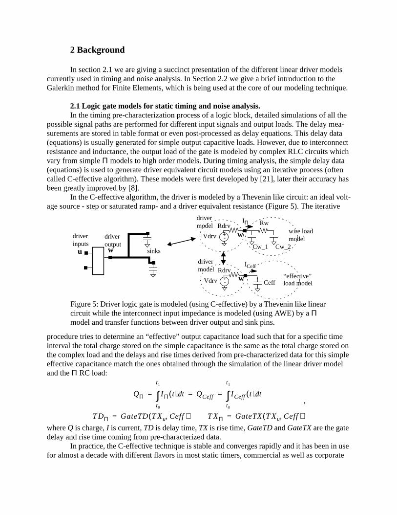
In Figure 13 the dc output port current of the NAND4 gate is plotted with respect to inand output pin voltages. In Figure 14 we are showing the points of convergence of the NANgate output (the points where the output port current is zero).
The non-linear model that we have generated is not going to match the dc port currethe original gate because it models the transient behavior rather than the steady state one.
0 .1 .5 .9 10.1
.5
.91
input (u)
outp
ut (
w)
Figure 12: Input-output signal pairs as paths through the domain of an invertor: a)rising input falling output paths, b) falling input rising output paths and c) static(positive and negative) noise paths for output holding high and low.
input (u) input (u)a) b) c)
0.1
.5
.91
0.1
.5
.91
0 .1 .5 .9 1 0 .1 .5 .9 1
outp
ut (
w)
outp
ut (
w)
D u w,( ) u umin umax,( ) w wmin wmax,( )∈,∈{ }=
I out:D ℜ→ with I out u w,( )Vd u w,( ) w–
Rd-------------------------------- Cd td
dw⋅–=
Vd u w,( ) Vij ψ ij u w,( )⋅i j,∑=
ment
func-
ure 15 we are showing the port current of our model which has been obtained for a one ele
partition of the domain and using second order Lagrange interpolating polynomials as base
0 0
1
1-0.005
0.005
0.0
Vinp
Vout
Iout
Vinp01 10.5 0.5
0.005
-0.005
0.005
-0.0050
0.0 0.0
Vout
Iout Iout
0.5
0.5
Figure 13: Variation of output port current w.r.t. input and output pin voltages(center). Contour plots of the output current for fixed input pin voltage levels (left)and fixed output pin voltage levels (right).
Figure 14: The convergence points of the original NAND4 gate which correspondto the points where the dc output gate current is 0.
0
0.5
1
0 0.5 1
Iout=0
Vin
p
Vout
0 0
0.0
1
1
-0.006
0.004
Vinp
Vout
Iout
Vinp0 0.5 1-0.006
0.004
0.0
-0.006
0.004
0.0
00.51Vout
Iout Iout
Figure 15: Variation of output pin current with the input and output pin voltages(center) for the non-linear driver model of the NAND4 gate. Contour plots of theoutput current for fixed input pin voltage levels (left) and fixed output pin voltagelevels (right).

re
e andn multi-Fig-
e holdg the both
ase thered is
. Thethis
vari-n is
tions. From the contour plots it can be seen that the port current is not monotonic inside thedomain and that results in multiple operating points for the same input-output voltage pair.
In Figure 16 the convergence curve of the driver port model and stability region(s) a
shown.It is in general desirable to have a close match between the original convergence curv
the model because that impacts the steady state accuracy which is important in cases wheple drivers are driving simultaneously the interconnect (see Example 5 from Section 4). Fromure 16 it is also apparent the impact of the holding resistance value. Our choice forRd was thehold down resistance value (108ohms) and the model tries to compensate with current in thhigh case where the actual resistance is larger. However, in Example 2 of Section 4 showinhold high and hold low functional noise pulses, we can see (Figure 19) that the accuracy incases is comparable.
Another important issue for our model is the domain of stability. For example, in our cthe basis functions are second order Lagrange polynomials and for any input voltage valueare exactly two points where the port current is zero. One point is the convergence point ancharacterized by:
, (22)
and the other one is the limit of the stable region and is characterized by:
. (23)
The stable region boundary is marked in Figure 16 by the border of the dark shaded areaslight shaded areas are marking the boundary of the absolutely stable region. The points in region are characterized by:
(24)
in which the port current source offers a negative feedback with respect to the output voltageation. In general, the situation in which the model has regions of instability inside its domaithe result of sparse measurements data present in those regions.
Figure 16: The convergence points of the driver model, the stable model domain(dark shaded area) and the absolute stability domain (light shaded area).
0.5
-0.5
1
1.5
-0.5
0
1.50 0.5 1
Iout=0
Vin
p
Vout
I u w,( ) 0= andwdd
I u w,( ) 0<
I u w,( ) 0= andwdd
I u w,( ) 0>
wdd
I u w,( ) 0≤

e arepaga-el inhoot)
sed to
eholde
4 forTheport
ormscase
more
ise
4. Results
In this section we are presenting some results obtained with our proposed model. Wshowing for comparison the performance of our model in the case of basic timing signal protion, functional noise and delay noise. We are also exemplifying the robustness of our modthe case when input signals are outside the characterization range (over-shoot and under-sand with highly inductive interconnect. We present the performance of the model in a multi-source net case and how the steady state is captured.
Using the test case described in Section 2, the new modeling technique has been ucharacterize the timing arc of our NAND4 gate from the input pin A1 to output pin X. We haveused a Thevenin type model on a domain with 1 two-dimensional element (similar to the onshown in figure 9) characterized by 9 points (a 3x3 grid), two of them with known values, thehigh and hold low conditions. So, 7 points were unknowns in th
characterization process. We have used 8 input-output signal pairs, 4 for rising output and falling output, with 2 equations for each pair (one for 0% to 50% and one for 10% to 90%). Rd andCd values have been determined using a simple small signal analysis on the output with the gate set-up to hold low.
Example 1: The first example is the test used in Figure 3. The near and far end wavefin the case “without noise” are shown in Figure 17.a. The near and far end waveforms in the
with delay noise are shown in Figure 17.b. The actual “delay noise” waveforms are shown indetail in Figure 18 for the far end signals.
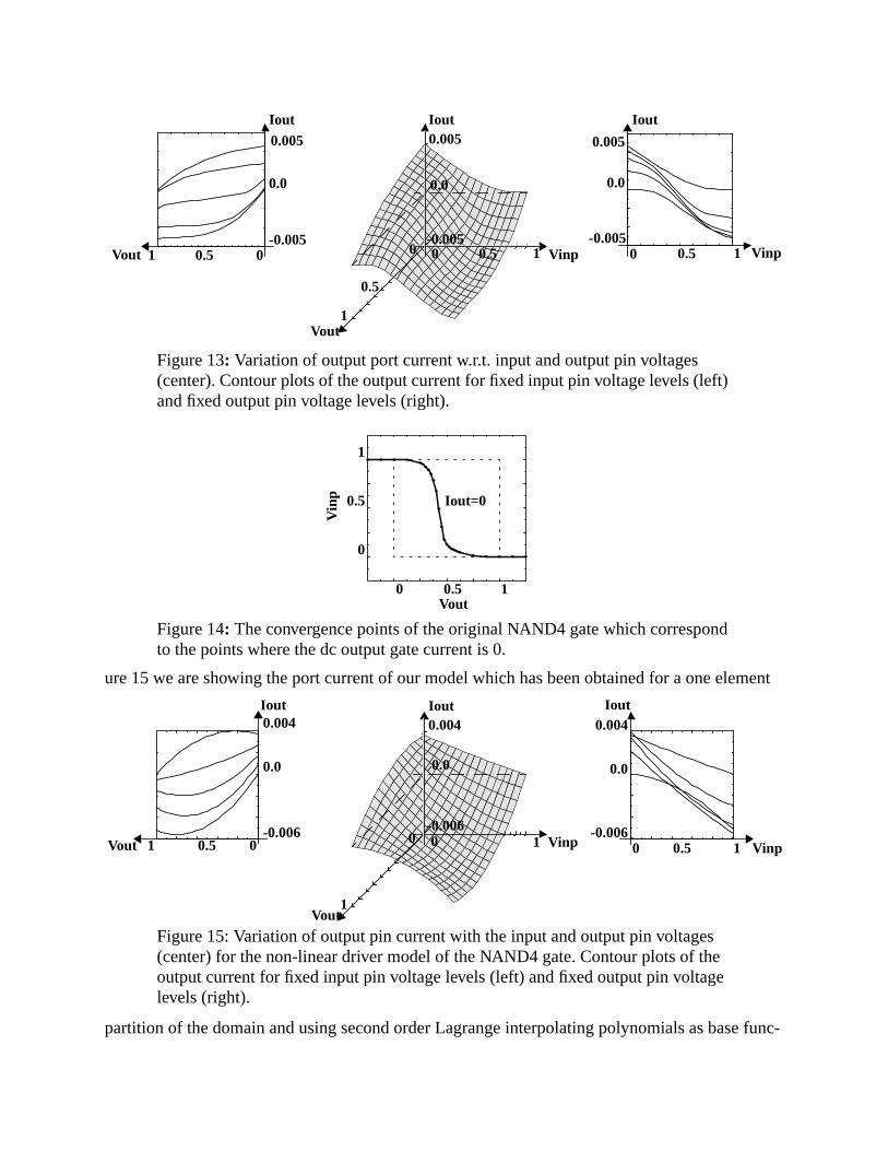
Example 2: In Figure 19 we are showing the accuracy of the model for functional noestimation. Our model is compared with the actual gate and the hold-up/down resistors.
Vd 0 1,( ) 1= Vd 1 0,( ) 0=
0.00.20.40.60.81.0
0 20 40 60 80 100
near end signalsfar end signals
volta
ge
time
Figure 17: The output pin of the NAND4 gate (near end) and the sink pin (far end).
0 20 40 60 80 100
0.00.20.40.60.81.0
near end signalsfar end signals
volta
ge
timea) without noise b) with delay noise
Figure 18: Delay noise comparison between our model and actual driver.
-0.15
-0.10
-0.05
0.00
0 20 40 60 80 100time
volta
ge
actual driver
our model
veof the There 20.
inter-nca-delslass ofRLC
in Fig-h the
Example 3: One of the more difficult cases to model in static timing (for the C-effectialgorithm) is the gate response with inductive output loads. In order to show the robustnessdriver model, a large amount of inductance has been added to the interconnect RC model.simulation results for the near and far end nodes of the interconnect wire are shown in Figu
Example 4: It is often the case that chains of gates are analyzed together with their connect. If the signals are heavily altered by noise or other effects, the simple ramp-like trutions performed on signals during static timing will result in significant errors. Since our moare characterized for a range of input signals, they are better suited for propagating a large cinput signals. In Figure 21 we used signals obtained at the beginning and end points of an
line to test the response of the model with signals that have less common shapes. Note thature 21.b the input signal has an over-shoot going outside the range of input values for whicgate was characterized.
-0.15
-0.10
-0.05
0.0
-0.15
-0.10
-0.05
0.0
0 20 40 60 80 100time
0 20 40 60 80 100time
volta
ge
volta
ge
hold-down noise hold-up noise
actual driver
our model
with hold-up resistorwith hold-down resistor
our model
actual driver
Figure 19: Functional noise at sink pin (far end) with the actual driver, holdingresistance model and our model for holding down (left) and holding up (right).
0.00.20.40.60.81.0
0 20 40 60 80 100
volta
ge
time
Figure 20: Signal propagation through highly inductive interconnect: near end sig-nals (left) and far end signals (right).
0.00.20.40.60.81.0
0 20 40 60 80 100
volta
ge
time
0 20 40 60 80 100
input signal
near end signals
time
volta
ge
0.00.20.40.60.81.0
-0.2
0.00.20.40.60.81.0
0 20 40 60 80 100
input signal
near end signals
time
-0.2
a) with under-shoot b) with over-shootFigure 21: The response of the gate to less common input signals.
volta
ge

en to
, the
ewith
et tot andr
unt of
hold-ng”istance
thenoise
ur time
Example 5: In the recent years, one trend in the microprocessor clock design has begenerate grid-like clock distribution networks with multiple drivers to reduce the clock skewacross the chip. Coupled with the higher impact of inductance on the long wide clock wiresanalysis of these nets in the static timing flow has been very difficult and inaccurate, forcingdesigners to perform extensive detailed circuit simulations. Our models capture very well thdriver behavior on nets with multiple sources as shown in Figure 22 on a 5x5 grid network
40 wire sections driven from the four corners. Two of the drivers have a significant input offsmagnify the voltage division across the interconnect. In Figure 22.b the waveforms at the firslast driver outputs and in the center of the grid are shown, both with real drivers and with oumodels. During the first part of the response, the two active drivers are driving each an amocapacitance outside their model characterization range but good accuracy is maintained.
Example 6: We have used the algorithm proposed in [24] to generate the “transient ing” resistance for comparison with our model. Through full net simulation, a “transient holdiresistance has been determined (712.8ohms) such that the area of the noise pulse with resmodel matches within 0.004% the area of the real delay noise pulse. The superposition of quiet response and the noise pulse with resistance model produces the approximation of theimpact on delay. The errors are tabulated in Table 1:
In Figure 23, all the near end point “delay noise” pulses (using actual driver model, onon-linear model and “transient holding” resistance model) are shown. The plot spans 150units which is the interval used for matching the noise pulse areas.
Table 1: Comparison with “transient holding” resistance model
Pin measurement type our model “transient” resistance
Near end 50% delay -1.8% -10.78%
10%-90% rise time 8.10% 18.68%
Far end 50% delay 0.54% -6.88%
10%-90% rise time 3.99% 8.45%
I1 & I 2
I3 & I 4
O1
O4
C
I1 I2
I3 I4
O1 O2
O3 O4
C
0 20 40 60 80 100
0.0
0.2
0.4
0.6
0.8
1.0
time
Figure 22: Signal propagation in a multi-source large RC grid (left). The driverinputs, outputs and the signal in the center of the grid are shown (right).
volta
ge

20 40 60 80 100time
120 140
-0.15
-0.10
-0.05
0.00
Figure 23: Comparison between the “delay noise” pulse obtained using our non-linear driver model and the “transient holding” resistance model at the near end.
actual driverour model
“transient holding”resistance model
volta
ge

oiser mod-
taticded.
dentolyno-
tputl mea-
they
del.t:e
,
and
od-that
ciently obser-and, in
lation
5. Conclusions and future work:
In this paper we have proposed a new technique to model logic gates for timing and nanalysis. The proposed models have quite a few distinct advantages over the existent driveels for timing and/or noise:• The modeling process is using the already existent measurements data generated for s
timing analysis for each logic block. No new data or special characterization work is nee• No non-linear spice simulations are required in the modeling process.• The models are simple Thevenin/Norton-like circuits with voltage/current sources depen
on the input and output pin voltages and are represented using elementary functions (pmials). This makes their simulation extremely efficient.
• The models have variable accuracy both in terms of the range of input rise time and oucapacitance load that is being covered and in terms of the error with respect to the actuasurement values used in the process.
• The models are covering large ranges of input rise time and output capacitive load and are re-usable (do not depend on a particular input-output situation or noise pulse).
• The models are very robust and maintain accuracy outside the characterization range.
The examples presented in Section 4 are showing the versatility of the proposed moWe have demonstrated the accuracy of our model in different situations of practical interes• normal signal propagation (static timing analysis) with very good behavior throughout th
characterization domain,• simulation of the driver response with complex output load models including inductance• computation of the delay variation due to switching noise,• functional noise analysis,• simulation of special cases such as nets with multiple drivers with significant time offsets
complex interconnect models.
As future work, our attention is focused on circuit simulation. One draw-back of our mels is that in order to simulate them we need a non-linear circuit simulator. The driver modelswe have used are piece-wise polynomial models. These models can be simulated very effiby available special purpose simulators (such as ACES [11]). One can also make a simplevation that the same FE method used to generate the models can be used to simulate themconjunction with reduced order interconnect models, one can develop a very efficient simuengine.
t.
al
-
tic
tice-
ulse 809-
nce
cter-,
pac-
-
t of
asednce
s andll
cu-
190-
99,
gn
References:
[1][Ain00] - Aingaran K.et al.“Coupling noise analysis for VLSI and ULSI circuits”, IEEE FirsInternational Symposium on Quality Electronic Design 2000, page(s) 485-489
[2][Aru97] - Arunachalam R., Dartu F. and Pileggi L.T. “CMOS gate delay models for generRLC loading” IEEE 1997 page(s) 224-229.
[3][Aru00] - Arunachalam R., Rajagopal K. and Pileggi L.T. “TACO: timing analysis with coupling” Design Automation Conference 2000, page(s) 266-269.
[4][Aru01] - Arunachalam R., Blanton R.D. and Pileggi L.T. “False coupling interactions in statiming analysis” Design Automation Conference 2001, page(s) 726-731.
[5][Bec81] - Becker E.B., Carey G.F. and Oden J.T. “Finite elements - an introduction -” PrenHall Inc. 1981.
[6][Che97] - Chen W., Gupta S.K. and Breuer M. “Analytic models for crosstalk delay and panalysis under non-ideal inputs” International Test Conference 1997, page(s)818.
[7][Che99] - Chen P. and Keutzer K. “Towards true crosstalk analysis” International Confereon CAD 1999, page(s) 132-137.
[8][Dar96] - Dartu F., Menezes N. and Pileggi L.T. “Performance computation for pre-charaized CMOS gates with RC loads” IEEE Transactions on CAD, vol. 15, issue 5May 1996, page(s) 544-553.
[9][Dar97] - Dartu F. and Pileggi L.T. “Calculating worst-case gate delays due to dominant caitance coupling” Design Automation Conference 1997, page(s) 46-51.
[10][Del00] - Delaurenti M.et al. “Switching noise analysis framework for high speed logic families” 14th International Conference on VLSI Design 2000, page(s) 524-530.
[11][Dev94] - Devgan A. and Rohrer R.A. “Adaptively controlled explicit simulation” IEEETransactions on CAD, vol.13, no.6, Jun.1994, page(s) 746-762.
[12][Dev97] - Devgan A. “Efficient coupled noise estimation for on-chip interconnects” DigesTechnical Papers, International Conference on CAD 1997, page(s) 147-151.
[13][Fel97] - Feldman P. and Freund L.W. “Circuit noise evaluation by Pade approximation bmodel-reduction techniques” Digest of Technical Papers, International Confereon CAD 1997, page(s) 132-138.
[14][Fre98] - Freund R.W. “Reduced-order modeling techniques based on Krylov sub-spacetheir use in circuit simulation” Numerical analysis manuscript No. 98-3-02, BeLaboratories, Feb. 1998.
[15][Gro98] - Gross P.D.et.al.“Determination of worst-case aggressor alignment for delay callation” International Conference on CAD 1998, page(s) 212-219.
[16][Kas00] - Kashyap, C.V. and Krauter, B.L. “A realizable driving point model for on-chipinterconnect with inductance” Design Automation Conference, 2000, page(s)195.
[17][Kra99] - Krauter, B.L., Mehrotra S. and Chandramouli V. “Including inductive effects ininterconnect timing analysis” IEEE Custom Integrated Circuits Conference 19page(s) 445-452.
[18][Kuh01] - Kuhlmann M. and Sapatnekar S.S. “Exact andefficient crosstalk estimation” IEEETransactions on CAD, vol.20, no.7, July 2001, page(s) 858-866.
[19][Lev00] - Levy R.et al. “ClariNet: a noise analysis tool for deep sub-micron design” DesiAutomation Conference 2000, page(s) 233-238.
er-e 8,
s)
eep,
e”
in
[20][Oda98] - Odabasioglu A., Celik M. and Pileggi L.T. “PRIMA: Passive reduced-order intconnect macro-modeling algorithm” IEEE Transactions on CAD, vol. 17, issuAug.1998, page(s) 645-654.
[21][Qia94] - Qian J., Pullela S. and Pillage L.T. “Modeling the ‘effective capacitance’ of RCinterconnect” IEEE Transactions on CAD, vol. 13, issue 12, Dec. 1994, page(1526-1535.
[22][Sas00] - Sasaki Y. and DeMicheli G. “Crosstalk delay analysis using relative windowmethod” ASIC/SOC Conference 1999, page(s) 9-13.
[23][She99] - Shepard K.L., Narayanan V. and Rose R. “Harmony: static noise analysis of dsubmicron digital integrated circuits” IEEE Transactions on CAD, vol.18, no.8Aug.1999, page(s) 1132-1150.
[24][Sir01] - Sirichotiyakul S.et al. “Driver modeling and alignment for worst-case delay noisDesign Automation Conference 2001, page(s) 720-725.
[25][Xia00.1] - Xiao T., Chang C.-W. and Marek-Sadowska M. “Efficient static timing analysispresence of crosstalk” ASIC/SOC Conference 2000, page(s) 335-339.
[26][Xia00.2] - Xiao T. and Marek-Sadowska M. “Worst delay estimation in crosstalk awarestatic timing analysis” International Conference on Computer Design 2000,page(s) 115-120.