Drive-On-Chip Reference Design - intel.de · AC and servo drive system designs comprise multiple...
48
About the Drive-On-Chip Reference Design 2019.11.07 AN-669 Subscribe Send Feedback e Drive-On-Chip reference design demonstrates concurrent multiaxis control of up to four three-phase AC 400-V permanent magnet synchronous motors (PMSMs) or sinusoidally wound brushless DC (BLDC) motors. AC and servo drive system designs comprise multiple distinct but interdependent functions to realize requirements to meet the performance and efficiency demands of modern motor control systems. e system's primary function is to efficiently control the torque and speed of the AC motor through appropriate control of power electronics. A typical drive system includes the following items: • Flexible pulse-width modulation (PWM) circuitry to switch the power stage transistors appropriately • Motor control loops for single- or multiaxis control • Industrial networking interfaces • Position encoder interfaces • Current, voltage, and temperature measurement feedback elements. • Monitoring functions, for example, for vibration suppression. e system requires system soſtware running on a processor for high-level system control, coordination, and management. Intel Cyclone ® and Intel ® MAX ® 10 devices offer high-performance fixed- and floating-point DSP functionality. Cyclone V SoC devices offer the integrated ARM-based hard processor subsystem (HPS); other Cyclone FPGA and Intel MAX 10 FPGA devices offer support for Nios II soſt processors. Cyclone and Intel MAX 10 FPGA devices offer a uniquely scalable and flexible platform for integration of single- and multiaxis drives on a single FPGA. e Intel motor control development framework allows you to create these integrated systems easily. e framework provides a reference design that comprises IP cores, soſtware libraries, and a hardware platform. e framework seamlessly integrates Intel system-level design tools such as DSP Builder and Qsys, and soſtware and IP components that allow you to extend and customize the reference design to meet your own application needs. e framework also supports optimal partitioning decisions between soſtware running on an integrated processor and IP performing portions of the motor control algorithm in the FPGA, to accelerate performance as required. For example, depending on the performance requirements of your system or the number of axes you need to support, you may implement all of the inner current control loop in hardware or entirely in soſtware. e framework flexibly allows you to connect to the motor and power stages through off-chip ADCs, and feedback encoder devices and to connect to higher-level automation controllers through off-the-shelf digital encoder and industrial Ethernet IP cores, respectively. e reference design offers vibration suppression, when you target the Cyclone V SoC devices. e design demonstrates how you can implement standard components (FFTs, FFT-post processing, IIR filter), to enable you to develop an automatic method for vibration suppression. You may use the FFTs and FFT Intel Corporation. All rights reserved. Intel, the Intel logo, Altera, Arria, Cyclone, Enpirion, MAX, Nios, Quartus and Stratix words and logos are trademarks of Intel Corporation or its subsidiaries in the U.S. and/or other countries. Intel warrants performance of its FPGA and semiconductor products to current specifications in accordance with Intel's standard warranty, but reserves the right to make changes to any products and services at any time without notice. Intel assumes no responsibility or liability arising out of the application or use of any information, product, or service described herein except as expressly agreed to in writing by Intel. Intel customers are advised to obtain the latest version of device specifications before relying on any published information and before placing orders for products or services. *Other names and brands may be claimed as the property of others. ISO 9001:2015 Registered www.altera.com 101 Innovation Drive, San Jose, CA 95134
Transcript of Drive-On-Chip Reference Design - intel.de · AC and servo drive system designs comprise multiple...
About the Drive-On-Chip Reference Design2019.11.07
AN-669 Subscribe Send Feedback
The Drive-On-Chip reference design demonstrates concurrent multiaxis control of up to four three-phaseAC 400-V permanent magnet synchronous motors (PMSMs) or sinusoidally wound brushless DC (BLDC)motors.
AC and servo drive system designs comprise multiple distinct but interdependent functions to realizerequirements to meet the performance and efficiency demands of modern motor control systems. Thesystem's primary function is to efficiently control the torque and speed of the AC motor throughappropriate control of power electronics. A typical drive system includes the following items:
• Flexible pulse-width modulation (PWM) circuitry to switch the power stage transistors appropriately• Motor control loops for single- or multiaxis control• Industrial networking interfaces• Position encoder interfaces• Current, voltage, and temperature measurement feedback elements.• Monitoring functions, for example, for vibration suppression.
The system requires system software running on a processor for high-level system control, coordination,and management.
Intel Cyclone® and Intel® MAX® 10 devices offer high-performance fixed- and floating-point DSPfunctionality. Cyclone V SoC devices offer the integrated ARM-based hard processor subsystem (HPS);other Cyclone FPGA and Intel MAX 10 FPGA devices offer support for Nios II soft processors. Cycloneand Intel MAX 10 FPGA devices offer a uniquely scalable and flexible platform for integration of single-and multiaxis drives on a single FPGA. The Intel motor control development framework allows you tocreate these integrated systems easily. The framework provides a reference design that comprises IP cores,software libraries, and a hardware platform. The framework seamlessly integrates Intel system-level designtools such as DSP Builder and Qsys, and software and IP components that allow you to extend andcustomize the reference design to meet your own application needs. The framework also supports optimalpartitioning decisions between software running on an integrated processor and IP performing portionsof the motor control algorithm in the FPGA, to accelerate performance as required. For example,depending on the performance requirements of your system or the number of axes you need to support,you may implement all of the inner current control loop in hardware or entirely in software. Theframework flexibly allows you to connect to the motor and power stages through off-chip ADCs, andfeedback encoder devices and to connect to higher-level automation controllers through off-the-shelfdigital encoder and industrial Ethernet IP cores, respectively.
The reference design offers vibration suppression, when you target the Cyclone V SoC devices. The designdemonstrates how you can implement standard components (FFTs, FFT-post processing, IIR filter), toenable you to develop an automatic method for vibration suppression. You may use the FFTs and FFT
Intel Corporation. All rights reserved. Intel, the Intel logo, Altera, Arria, Cyclone, Enpirion, MAX, Nios, Quartus and Stratix words and logos are trademarks ofIntel Corporation or its subsidiaries in the U.S. and/or other countries. Intel warrants performance of its FPGA and semiconductor products to currentspecifications in accordance with Intel's standard warranty, but reserves the right to make changes to any products and services at any time without notice.Intel assumes no responsibility or liability arising out of the application or use of any information, product, or service described herein except as expresslyagreed to in writing by Intel. Intel customers are advised to obtain the latest version of device specifications before relying on any published informationand before placing orders for products or services.*Other names and brands may be claimed as the property of others.
ISO9001:2015Registered
www.altera.com101 Innovation Drive, San Jose, CA 95134

postprocessing for condition monitoring, which detects vibrations that indicate degradation or wear andcommunicate the results to another system.
The reference design integrates Motor Control IP Suite components, a Nios® II soft processor subsystem,or ARM-based HPS, and software that uses an FOC algorithm. The reference design uses the Intel DSPBuilder system-level design tool to implement the FOC algorithm.
DSP Builder provides a MATLAB and Simulink flow that allows you to create hardware optimized fixedlatency representations of algorithms without requiring HDL/hardware skills. Intel provides DSP Builderfixed-point and floating point algorithms to demonstrate both options. The DSP Builder folding featurereduces the resource usage of the logic as an alternative to a fully parallel implementation. The referencedesign also includes an efficient Avalon® Memory-Mapped interface that you can integrate in Qsys.
Related InformationOptimize Motor Control Designs with an Integrated FPGA Design Flow
2 About the Drive-On-Chip Reference DesignAN-669
2019.11.07
Altera Corporation About the Drive-On-Chip Reference Design
Send Feedback
Motor Control Boards2019.11.07
AN-669 Subscribe Send Feedback
Table 1: FPGA Host Control Board Options
Board Vendor Website
Cyclone V SoC developmentboard
Intel https://www.intel.com/content/www/us/en/programmable/products/boards_and_kits/dev-kits/altera/kit-cyclone-v-soc.htmlhttps://www.intel.com/content/www/us/en/programmable/products/boards_and_kits/dev-kits/altera/kit-cyclone-v-soc.html
MAX 10 FPGA developmentboard
Intel https://www.intel.com/content/www/us/en/programmable/products/boards_and_kits/dev-kits/altera/max-10-fpga-development-kit.html
Terasic SoCKit Terasic http://www.terasic.com
Table 2: Motor Control Power Board Options
Board Vendor Website
Multiaxis Motor ControlBoard
Intel https://www.altera.com/products/boards_and_kits/dev-kits/altera/kit-multi-axis-motor-control.html
FalconEye 2 HSMCMotor Control Board
devboards http://www.devboards.de
An HSMC connector connects:
• The Cyclone V SoC development board to the Multiaxis Motor Control Board or the FalconEye 2HSMC Motor Control Board
• The Cyclone V SoC and MAX 10 FPGA Development Boards and SoCKit to the FalconEye 2 HSMCMotor Control Board.
Note: The Multiaxis Motor Control Board supports multiple position feedback interfaces, however, thereference design only supports EnDat or BiSS.
For availability of the Multiaxis Motor Control Board, contact your Intel sales representative.
Related Information
• Multiaxis Motor Control Board Reference ManualFor more information on the Multiaxis Motor Control Board
Intel Corporation. All rights reserved. Intel, the Intel logo, Altera, Arria, Cyclone, Enpirion, MAX, Nios, Quartus and Stratix words and logos are trademarks ofIntel Corporation or its subsidiaries in the U.S. and/or other countries. Intel warrants performance of its FPGA and semiconductor products to currentspecifications in accordance with Intel's standard warranty, but reserves the right to make changes to any products and services at any time without notice.Intel assumes no responsibility or liability arising out of the application or use of any information, product, or service described herein except as expresslyagreed to in writing by Intel. Intel customers are advised to obtain the latest version of device specifications before relying on any published informationand before placing orders for products or services.*Other names and brands may be claimed as the property of others.
ISO9001:2015Registered
www.altera.com101 Innovation Drive, San Jose, CA 95134

• Motor Control IP Suite Components Data Sheet.For more information on the Motor Control IP components
2 Motor Control BoardsAN-669
2019.11.07
Altera Corporation Motor Control Boards
Send Feedback
Features2019.11.07
AN-669 Subscribe Send Feedback
The reference design offers the following features:
• Multiple field-oriented control (FOC) loop implementations:
• Fixed- or floating-point implementation targeting the ARM Cortex A9 processor on SoC devices• Fixed- or floating-point implementation with Nios II processors targeting MAX 10 FPGA devices• Fixed and floating-point accelerator implementations designed using Simulink model-based design
flow with DSP Builder• Integration in a single FPGA of single and multiaxis motor control IP including:
• PWM for two-level IGBT• Sigma delta ADC interfaces for motor current feedback and DC link voltage measurement• Position feedback with EnDat or BiSS
• Vibration suppression (SoC devices only):
• DSP Builder-designed FFT accelerator• Peak detection• Suppression filter
• System Console GUI for motor feedback information, vibration suppression demonstration, andcontrol of motors
Intel Corporation. All rights reserved. Intel, the Intel logo, Altera, Arria, Cyclone, Enpirion, MAX, Nios, Quartus and Stratix words and logos are trademarks ofIntel Corporation or its subsidiaries in the U.S. and/or other countries. Intel warrants performance of its FPGA and semiconductor products to currentspecifications in accordance with Intel's standard warranty, but reserves the right to make changes to any products and services at any time without notice.Intel assumes no responsibility or liability arising out of the application or use of any information, product, or service described herein except as expresslyagreed to in writing by Intel. Intel customers are advised to obtain the latest version of device specifications before relying on any published informationand before placing orders for products or services.*Other names and brands may be claimed as the property of others.
ISO9001:2015Registered
www.altera.com101 Innovation Drive, San Jose, CA 95134
Getting Started2019.11.07
AN-669 Subscribe Send Feedback
Software Requirements on page 1
Downloading and Installing the Reference Design on page 2
Setting Up the Boards on page 4
Compiling the Design on page 5Either compile your design or use the Intel-provided pre-compiled .sof from the master_imagedirectory of your reference design variant.
Compiling the µC/OS-II HPS Software on page 5If you are targeting the Cyclone V SoC development board or SocKit, compile the µC/OS-II version of theHPS software.
Compiling the Nios II Software on page 6
Programming the Hardware onto the Device on page 7
Downloading the DS-5 HPS Software to the Device on page 7
Downloading the Nios II Software to the Device on page 9Prerequisites: import and compile the Nios II software in the Nios II Software Build Tools for Eclipse.
Creating and Booting an HPS SD Card Software Image on page 9You create a bootable SD card that contains the software image, so you can boot the software automaticallywithout using the DS-5 Debugger
Software Requirements
The reference design requires:
• The Altera Complete Design Suite version 15.0, which includes:
• The Quartus II software v15.0• DSP Builder v15.0• The Altera Nios II Embedded design Suite (EDS) v15.0
• The Altera SoC EDS v15.0 (for designs that target the Cyclone V SoC), which includes ARM Develop‐ment Studio 5 (DS-5) Altera Edition.
• Terminal emulator such as Tera Term for SoC based designs
Intel Corporation. All rights reserved. Intel, the Intel logo, Altera, Arria, Cyclone, Enpirion, MAX, Nios, Quartus and Stratix words and logos are trademarks ofIntel Corporation or its subsidiaries in the U.S. and/or other countries. Intel warrants performance of its FPGA and semiconductor products to currentspecifications in accordance with Intel's standard warranty, but reserves the right to make changes to any products and services at any time without notice.Intel assumes no responsibility or liability arising out of the application or use of any information, product, or service described herein except as expresslyagreed to in writing by Intel. Intel customers are advised to obtain the latest version of device specifications before relying on any published informationand before placing orders for products or services.*Other names and brands may be claimed as the property of others.
ISO9001:2015Registered
www.altera.com101 Innovation Drive, San Jose, CA 95134
Downloading and Installing the Reference Design
1. Download the relevant reference design .par file for your development kit and power board from theIntel Design Store.To obtain further support on the reference design, contact your local Intel sales representative.
2. Install the relevant reference design .par file for your development kit and power board.
Table 1: Design .par Files
Variant Development Kit Power Board Processor
DOC_4AXIS_CVSX Cyclone V SoC Intel 4 Axis HPS
DOC_FE2H_CVSX Cyclone V SoC FalconEye 2 HSMC HPS
DOC_FE2H_CVSX_XiP Cyclone V SoC FalconEye 2 HSMC HPS
DOC_FE2H_MAX10 MAX 10 FPGA FalconEye 2 HSMC Nios II
DOC_FE2H_SoCKit SoCKit FalconEye 2 HSMC HPS
Note: The XiP variant does not use external DDR3 memory and executes all code directly from flashmemory.
3. In the Quartus II software, click File > New Project Wizard.4. Click Next.5. Enter the path for your project working directory and enter variant name from the table for the project
name.6. Click Next.7. Select Project Template.8. Click Next9. Click Install the design templates.10.Browse to select the .par file for the reference design and browse to the destination directory where you
want to install it.Figure 1: Design Template Installation
11.Click OK on the design template installation message.12.Select the Drive on Chip Reference design design example.
2 Downloading and Installing the Reference DesignAN-669
2019.11.07
Altera Corporation Getting Started
Send Feedback
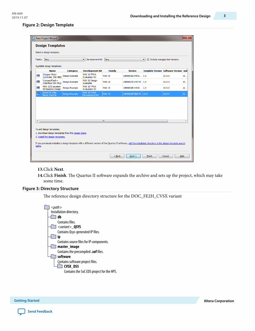
Figure 2: Design Template
13.Click Next.14.Click Finish. The Quartus II software expands the archive and sets up the project, which may take
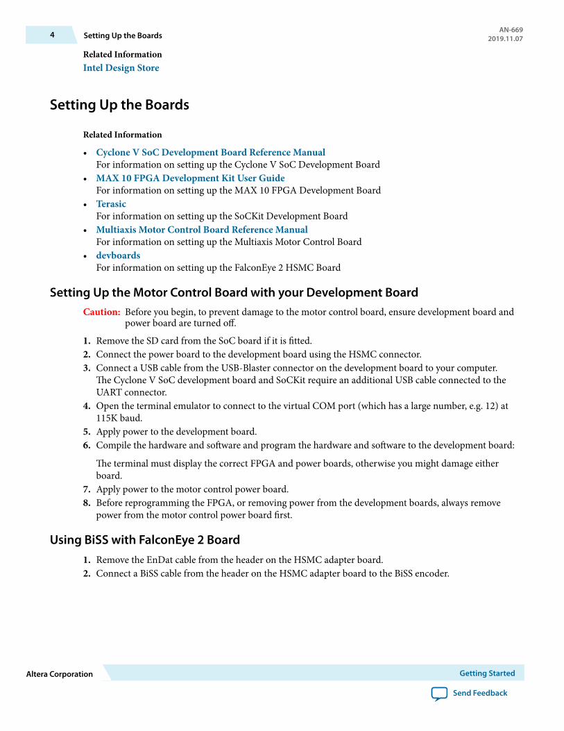
some time.Figure 3: Directory Structure
The reference design directory structure for the DOC_FE2H_CVSX variant
<path>Installation directory.
dbContains files.<variant>_QSYSContains Qsys-generated IP files.ipContains source files for IP components.master_imageContains the precompiled .sof files.
CVSX_DS5Contains the SoC EDS project for the HPS.
softwareContains software project files.
AN-6692019.11.07 Downloading and Installing the Reference Design 3
Getting Started Altera Corporation
Send Feedback
Related InformationIntel Design Store
Setting Up the Boards
Related Information
• Cyclone V SoC Development Board Reference ManualFor information on setting up the Cyclone V SoC Development Board
• MAX 10 FPGA Development Kit User GuideFor information on setting up the MAX 10 FPGA Development Board
• TerasicFor information on setting up the SoCKit Development Board
• Multiaxis Motor Control Board Reference ManualFor information on setting up the Multiaxis Motor Control Board
• devboardsFor information on setting up the FalconEye 2 HSMC Board
Setting Up the Motor Control Board with your Development BoardCaution: Before you begin, to prevent damage to the motor control board, ensure development board and
power board are turned off.
1. Remove the SD card from the SoC board if it is fitted.2. Connect the power board to the development board using the HSMC connector.3. Connect a USB cable from the USB-Blaster connector on the development board to your computer.
The Cyclone V SoC development board and SoCKit require an additional USB cable connected to theUART connector.
4. Open the terminal emulator to connect to the virtual COM port (which has a large number, e.g. 12) at115K baud.
5. Apply power to the development board.6. Compile the hardware and software and program the hardware and software to the development board:
The terminal must display the correct FPGA and power boards, otherwise you might damage eitherboard.
7. Apply power to the motor control power board.8. Before reprogramming the FPGA, or removing power from the development boards, always remove
power from the motor control power board first.
Using BiSS with FalconEye 2 Board1. Remove the EnDat cable from the header on the HSMC adapter board.2. Connect a BiSS cable from the header on the HSMC adapter board to the BiSS encoder.
4 Setting Up the BoardsAN-669
2019.11.07
Altera Corporation Getting Started
Send Feedback
Compiling the DesignEither compile your design or use the Intel-provided pre-compiled .sof from the master_imagedirectory of your reference design variant.
1. By default, Intel configures <variant>.v for EnDat encoders for FalconEye 2 HSMC Motor ControlBoard projects; BiSS for all Multiaxis Motor Control Board projects. In <variant>.v, to use BiSS, addthe following line; to use EnDat, remove it (if present).
"define BISS"
2. Add the paths to the license files for the EnDat and BiSS IP components to the Quartus II license path.a. Click Tools > License Setup.b. Copy any existing license paths into a text editor.c. Browse to the EnDat license file ip\endat_OCP\dsgn\vhdl_ava_ALT_enc_ocp\ocp _
license.dat and click Open.d. Copy and paste this license path into your text editor. Add a semicolon to separate this text from the
original text.e. Browse to the BiSS license file ip\biss_OCP\license.dat and click Open.f. Copy and paste this license path into your text editor. Add a semicolon to separate this text from the
original text and teh EnDat license.g. Copy and paste the text from the text editor to the Quartus II License File dialog box.
The final license path is <Project directory>\ip\endat_OCP\dsgn\vhdl_ava_ALT_enc_ocp;<Project directory>\ip\biss_OCP\license.dat;<original license paths>.Alternatively, you can add this path to the Windows environment variable LM_LICENSE_FILE.
3. Click Processing > Start Compilation .
Note: You may edit the reference design project in Qsys.
Compiling the µC/OS-II HPS SoftwareIf you are targeting the Cyclone V SoC development board or SocKit, compile the µC/OS-II version of theHPS software.
1. To ensure that the environment is set up correctly, run SoC EDS command shell, then start DS-5 bytyping eclipse& at the command prompt.
Note: Do not use the Windows start menu entry to start DS-5.2. Specify the \CVSX_DS5 directory as the workspace by browsing to the <path>\software\CVSX_DS5
directory.3. Click OK to create the workspace.
Note: Close the welcome to DS-5 tab if it shows.4. Import the makefile project CVSX_DS5:
AN-6692019.11.07 Compiling the Design 5
Getting Started Altera Corporation
Send Feedback
a. Select File > Import to open the Import window.b. Select General > Existing Projects into Workspace and click Next.c. Click Select Root Directory and browse to the project directory, DOC_CVSX in the workspace
directory, CVSX_DS5.d. Click OK.e. Click Finish.
Table 2: Software Project Directories
The linked directories that appear in the Project Explorer view under DOC_CVSXDirectory Description
app Application main entry point.
components Motor control component source and header files.
hwlibs The build process copies selected files from the Altera Complete Design Suite hardwarelibraries to this directory.
mc Motor control source and header files.
objects The build process creates object files here.
perf Performance monitor source and header files.
platform Platform (development kit and RTOS) specific source and header files.
source Source code. This directory contains other linked subdirectories.
vibration Vibration suppression demo source and header files.
5. Single-axis power boards default to EnDat; multiaxis power boards default to BiSS. To override thedefault encoder, edit mc\mc.h to define the OVERRIDE_ENCODER macro:
#define OVERRIDE_ENCODER SYSID_ENCODER_ENDAT
#define OVERRIDE_ENCODER SYSID_ENCODER_BISS6. Rebuild the DOC_CVSX project: right-click DOC_CVSX project and click Build Project.
Compiling the Nios II Software1. Start Nios II EDS. Click Start > Altera > Nios II EDS > Nios II Software Build Tools2. Specify the \software folder as the workspace by browsing to the reference design \software directory.3. Click OK to create the workspace.4. Import application and board support package (BSP) projects:
a. Click File > Import.b. Expand General and click Existing Projects into Workspace.c. Click Next.d. Browse to \software\<variant> and click OK.e. Click Finish.f. Repeat steps a to e for <variant>_bsp.
6 Compiling the Nios II SoftwareAN-669
2019.11.07
Altera Corporation Getting Started
Send Feedback
5. Single-axis power boards default to EnDat; multiaxis power boards default to BiSS. To override thedefault encoder, edit mc.h to define the OVERRIDE_ENCODER macro:
#define OVERRIDE_ENCODER SYSID_ENCODER_ENDAT
#define OVERRIDE_ENCODER SYSID_ENCODER_BISS6. Rebuild the BSP project: right-click <variant>_bsp project, point to Nios II, and click Generate BSP.7. Build the application project: right-click <variant> project and click Build Project.
Note: On Windows, the first time you build the project might take up to one hour.
Note: Repeat steps 6 and 7 if you make any changes to the Qsys project.
Programming the Hardware onto the Device
Before you begin
Set up the motor control board.
1. In the Quartus II software, click Tools > Programmer.2. In the Programmer pane, select USB-Blaster II (or CV SoCKit for the Terasic SoCKit) under
Hardware Setup and JTAG under Mode.3. Click Auto Detect to detect devices.4. If you are targeting a Cyclone V SoC, select any 5CSX device from the pop-up list. For MAX 10
devices, select any 10M50 device.5. Double-click on the File field for the 5CSX or 10M50 device from the pop-up list.6. Select the output_files/<project name>_time_limited.sof and click Open.7. Click OK on the time-limited .sof message.8. Turn on Program/Configure.9. Click Start.
Note: Do not close the OpenCore Plus message that appears.
Related InformationSetting Up the Motor Control Board with your Development Board on page 4
Downloading the DS-5 HPS Software to the Device
Before you begin
Import and compile the HPS software in DS-5. You must have a DS-5 debugger license to download HPSsoftware.
1. Select Run > Debug Configurations.2. Create new DS-5 debugger configuration:
AN-6692019.11.07 Programming the Hardware onto the Device 7
Getting Started Altera Corporation
Send Feedback
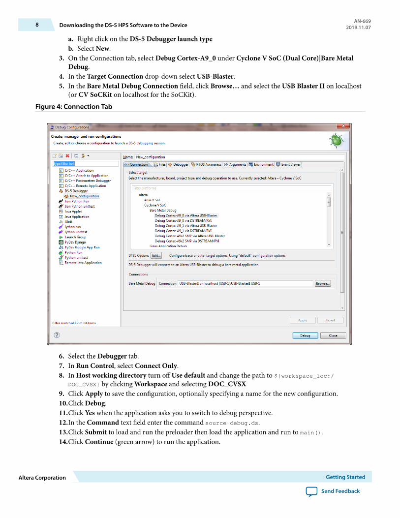
a. Right click on the DS-5 Debugger launch typeb. Select New.
3. On the Connection tab, select Debug Cortex-A9_0 under Cyclone V SoC (Dual Core)|Bare MetalDebug.
4. In the Target Connection drop-down select USB-Blaster.5. In the Bare Metal Debug Connection field, click Browse… and select the USB Blaster II on localhost
(or CV SoCKit on localhost for the SoCKit).Figure 4: Connection Tab
6. Select the Debugger tab.7. In Run Control, select Connect Only.8. In Host working directory turn off Use default and change the path to ${workspace_loc:/
DOC_CVSX} by clicking Workspace and selecting DOC_CVSX9. Click Apply to save the configuration, optionally specifying a name for the new configuration.10.Click Debug.11.Click Yes when the application asks you to switch to debug perspective.12.In the Command text field enter the command source debug.ds.13.Click Submit to load and run the preloader then load the application and run to main().14.Click Continue (green arrow) to run the application.
8 Downloading the DS-5 HPS Software to the DeviceAN-669
2019.11.07
Altera Corporation Getting Started
Send Feedback
15.Check that the terminal console display shows the correct FPGA and power board combination. Forexample:
0: [DECODE SYSID] Decoding hardware platform from QSYS SYSID data : 0x00D112FE0: [DECODE SYSID] Design Version : 15.00: [DECODE SYSID] FPGA Board : Cyclone V SX SoC Dev Kit0: [DECODE SYSID] Power Board : FalconEye v2.0 HSMC Single-axis0: [DECODE SYSID] Encoder Type : EnDat0: [DECODE SYSID] 1 axes available0: [DECODE SYSID] Axis 0 : Enabled
16.When the application is running, right-click on Cortex-A9_0 and click Disconnect from Target.17.Apply power to the power board. The motor starts to turn.
Downloading the Nios II Software to the DevicePrerequisites: import and compile the Nios II software in the Nios II Software Build Tools for Eclipse.
To program the Nios II software to the device:
1. In the Nios II EDS, on the Run menu, click Run configurations....a. Double click Nios II Hardware to generate a new run configuration.b. Click New_configuration.c. On the Project tab select the DOC_FE2H_MAX10 project in the Project name drop-down.d. Turn on Enable browse for file system ELF file. Browse to the software\DOC_DE2115 and select
DOC_DE2115.elf.e. On the Target Connection tab, click Refresh Connections. The software finds the USB-Blaster
cable.f. Click Apply to save changes, optionally specifying a name for the new configuration.g. Click Run to start the software.
2. Check that the terminal console display shows the correct FPGA and power board combination. Forexample:
0: [DECODE SYSID] Decoding hardware platform from QSYS SYSID data : 0x00D111FE0: [DECODE SYSID] Design Version : 15.00: [DECODE SYSID] FPGA Board : Cyclone V E Dev Kit0: [DECODE SYSID] Power Board : FalconEye v2.0 HSMC Single-axis0: [DECODE SYSID] Encoder Type : EnDat0: [DECODE SYSID] 1 axes available0: [DECODE SYSID] Axis 0 : Enabled
3. Apply power to the power board. The motor starts to turn.
Creating and Booting an HPS SD Card Software ImageYou create a bootable SD card that contains the software image, so you can boot the software automaticallywithout using the DS-5 Debugger
1. Create a bootable SD card image using the prebuilt image that the SoC EDS includes.a. On Windows, download and install win32diskimager.b. Find the bootable image for your development board.
AN-6692019.11.07 Downloading the Nios II Software to the Device 9
Getting Started Altera Corporation
Send Feedback

For the Cyclone SoC development board find sd_card_linux_boot_image.img in the IntelSoC EDS default installation directory: C:\altera\15.0\embedded\embeddedsw\socfpga\prebuilt_images For the Terasic SoCKit, find sd_image_sockit_20140902.img (see relatedinformation).
c. Use win32diskimager or Linux to write the bootable image onto your SD card.2. Copy DOC_CVSX_uImage to the FAT partition on the SD card.3. Enter U-Boot:
a. Insert the SD card in the boardb. Apply power to the board.c. Open your Terminal Emulator software and connect to the board.Press the ‘Cold Reset’ (Intel SoC
dev board) or ‘HPS_RST’ (SoCKit), while monitoring the terminal.d. Press HPS_RST (SoCKit) or Cold Reset (Intel development boards) and monitor the terminal.e. Press a key in the terminal window when prompted, before the countdown finishes and the
operating system boots.4. At the U-Boot prompt, edit the U-Boot environment by typing:
setenv mmcload "mmc rescan;fatload mmc 0:1 0x01000000 doc_cvsx_uImage 0 0x40; go 0x01000000"5. Save the new environment setting by typing:
env save6. Configure the FPGA.7. Boot the software: press HPS_RST (SoCKit) or Cold Reset (Intel development boards) again.
Related Information
• Programming the Hardware onto the Device on page 7• Windows Disk Imager• Terasic SoCKit bootable image
10 Creating and Booting an HPS SD Card Software ImageAN-669
2019.11.07
Altera Corporation Getting Started
Send Feedback
Debugging and Monitoring Hardware with SystemConsole
2019.11.07
AN-669 Subscribe Send Feedback
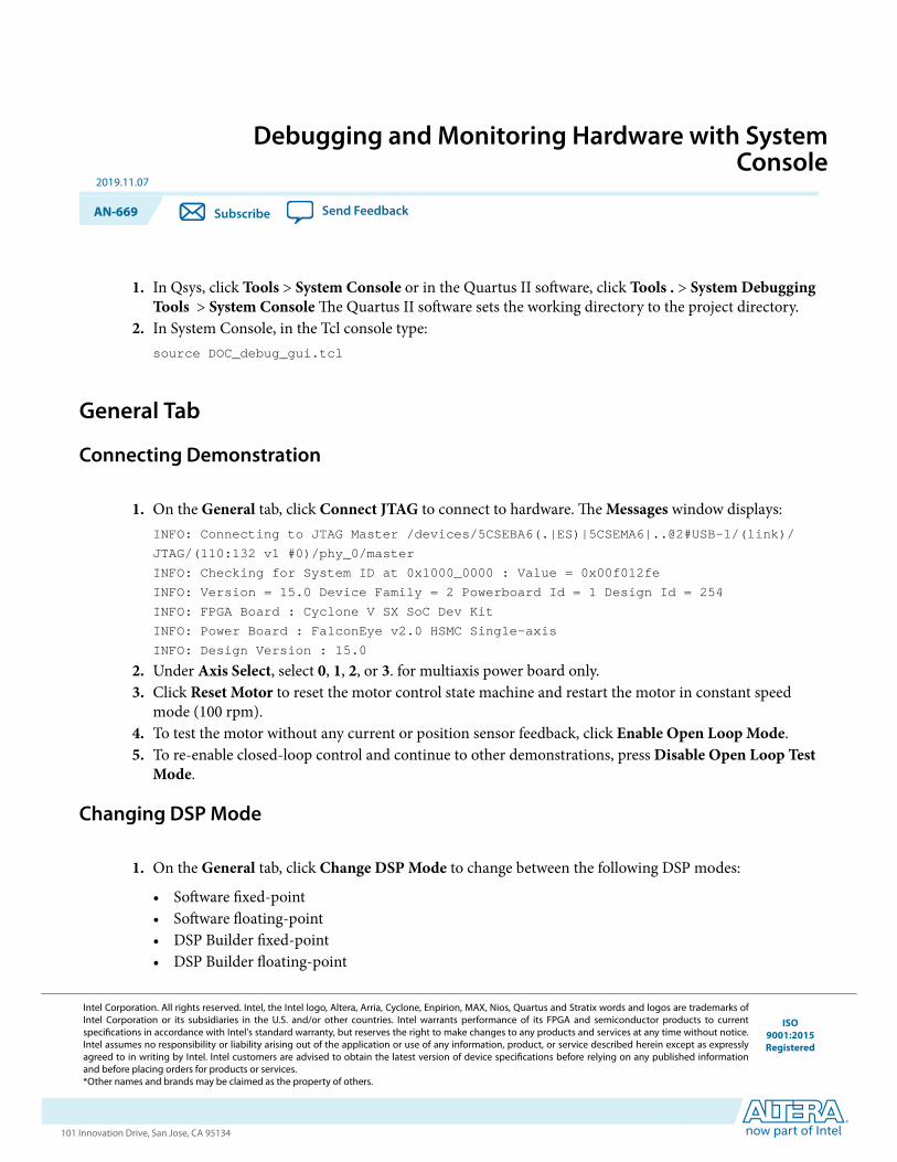
1. In Qsys, click Tools > System Console or in the Quartus II software, click Tools . > System DebuggingTools > System Console The Quartus II software sets the working directory to the project directory.
2. In System Console, in the Tcl console type:source DOC_debug_gui.tcl
General Tab
Connecting Demonstration
1. On the General tab, click Connect JTAG to connect to hardware. The Messages window displays:INFO: Connecting to JTAG Master /devices/5CSEBA6(.|ES)|5CSEMA6|..@2#USB-1/(link)/
JTAG/(110:132 v1 #0)/phy_0/master
INFO: Checking for System ID at 0x1000_0000 : Value = 0x00f012fe
INFO: Version = 15.0 Device Family = 2 Powerboard Id = 1 Design Id = 254
INFO: FPGA Board : Cyclone V SX SoC Dev Kit
INFO: Power Board : FalconEye v2.0 HSMC Single-axis
INFO: Design Version : 15.0
2. Under Axis Select, select 0, 1, 2, or 3. for multiaxis power board only.3. Click Reset Motor to reset the motor control state machine and restart the motor in constant speed
mode (100 rpm).4. To test the motor without any current or position sensor feedback, click Enable Open Loop Mode.5. To re-enable closed-loop control and continue to other demonstrations, press Disable Open Loop Test
Mode.
Changing DSP Mode
1. On the General tab, click Change DSP Mode to change between the following DSP modes:
• Software fixed-point• Software floating-point• DSP Builder fixed-point• DSP Builder floating-point
Intel Corporation. All rights reserved. Intel, the Intel logo, Altera, Arria, Cyclone, Enpirion, MAX, Nios, Quartus and Stratix words and logos are trademarks ofIntel Corporation or its subsidiaries in the U.S. and/or other countries. Intel warrants performance of its FPGA and semiconductor products to currentspecifications in accordance with Intel's standard warranty, but reserves the right to make changes to any products and services at any time without notice.Intel assumes no responsibility or liability arising out of the application or use of any information, product, or service described herein except as expresslyagreed to in writing by Intel. Intel customers are advised to obtain the latest version of device specifications before relying on any published informationand before placing orders for products or services.*Other names and brands may be claimed as the property of others.
ISO9001:2015Registered
www.altera.com101 Innovation Drive, San Jose, CA 95134
Using Speed Control
1. Under Speed Demo Setup enter Speed Value 1, Speed Value 2, and Speed Interval, to set the speedand time interval between speed value switches. You can select speeds from –3,000 to +3,000 rpm.
2. Click Run Speed Demo to start a sequence where System Console switches the motor speed commandalternately between the two speeds at the specified time interval.
3. Alternatively, select a new Speed Request value in the drop-down list.
Using Position Control
1. Type in two position values (from –36,000 to + 36,000 degree), a speed limit and a position interval.2. Click Run Position Demo.
System Console Dials
On the General tab, System Console displays the following dials:
• DSP Latency:
• Measures the runtime of the field-oriented control (FOC) algorithm with software timers in theinterrupt service routine (ISR)
• Shows the time taken to execute the algorithm in the different DSP modes• Speed. The instantaneous speed (rpm) of the motor• Position. The position of the motor shaft in degrees. System Console sets the scale automatically based
on the parameters you configure in the position demonstration.
Note: If you set Position Interval to less than several seconds, you may not see the changes on the dialbecause of the update rate of the GUI.
Control and Diagnostics TabOn the Control and Diagnostics tab you can configure an integrated storage buffer that behaves similarlyto a storage oscilloscope. System Console captures a range of variables within the FOC DSP loop at a 16-kHz sample rate and then displays them interactively on graphs. You can configure the trace triggersettings and storage depth. System Console displays the results and automatically writes them to a .csvfile for later analysis.
Monitoring Performance
1. On the Control and Diagnostics tab, under Trigger Signal, select the signal you want to trigger thetrace data capture. If you select Always, the trigger is always active.
2. Under Trigger Edge, select one of the following trigger types:
2 Using Speed ControlAN-669
2019.11.07
Altera Corporation Debugging and Monitoring Hardware with System Console
Send Feedback
a. Level (trigger signal must match this value)b. Rising Edge (trigger signal must transition from below to above this value)c. Falling Edge (trigger signal must transition from above to below this value)d. Either Edge (triggers on both falling and rising edge conditions).
3. Under Trigger Value, select the value that Trigger Edge uses to compare the signal value against.
Note: These values are raw integer values, not the scaled values that System Console displays in thegraphs. Convert the raw integer values into scaled values.
4. Click Update Trigger, if you update the Trigger Value.5. Under Trace Depth, select the number of samples to capture and display. System Console can store up
to 4,096 samples on SoC or 2,048 samples on MAX 10 devices. Select a lower number of samples tomake the System Console update rate faster, and zoom in on the graph as the graph scale autosizes tothe number of samples.
6. Specify a Trace Filename. System Console saves the trace data saved to a .csv file.7. Click Start Trace to start the trace; click Disable Trace again to stop the trace.
Related InformationSignals and Raw Versus Physical Values on page 3
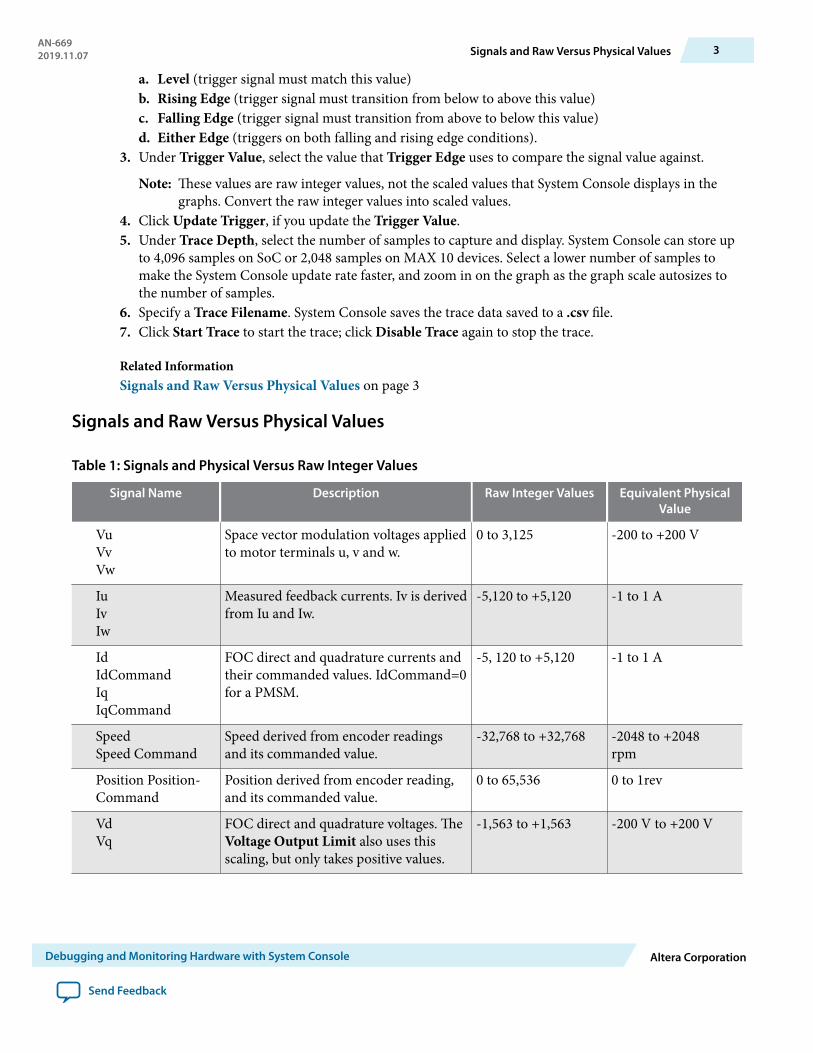
Signals and Raw Versus Physical Values
Table 1: Signals and Physical Versus Raw Integer Values
Signal Name Description Raw Integer Values Equivalent PhysicalValue
VuVvVw
Space vector modulation voltages appliedto motor terminals u, v and w.
0 to 3,125 -200 to +200 V
IuIvIw
Measured feedback currents. Iv is derivedfrom Iu and Iw.
-5,120 to +5,120 -1 to 1 A
IdIdCommandIqIqCommand
FOC direct and quadrature currents andtheir commanded values. IdCommand=0for a PMSM.
-5, 120 to +5,120 -1 to 1 A
SpeedSpeed Command
Speed derived from encoder readingsand its commanded value.
-32,768 to +32,768 -2048 to +2048rpm
Position Position‐Command
Position derived from encoder reading,and its commanded value.
0 to 65,536 0 to 1rev
VdVq
FOC direct and quadrature voltages. TheVoltage Output Limit also uses thisscaling, but only takes positive values.
-1,563 to +1,563 -200 V to +200 V
AN-6692019.11.07 Signals and Raw Versus Physical Values 3
Debugging and Monitoring Hardware with System Console Altera Corporation
Send Feedback
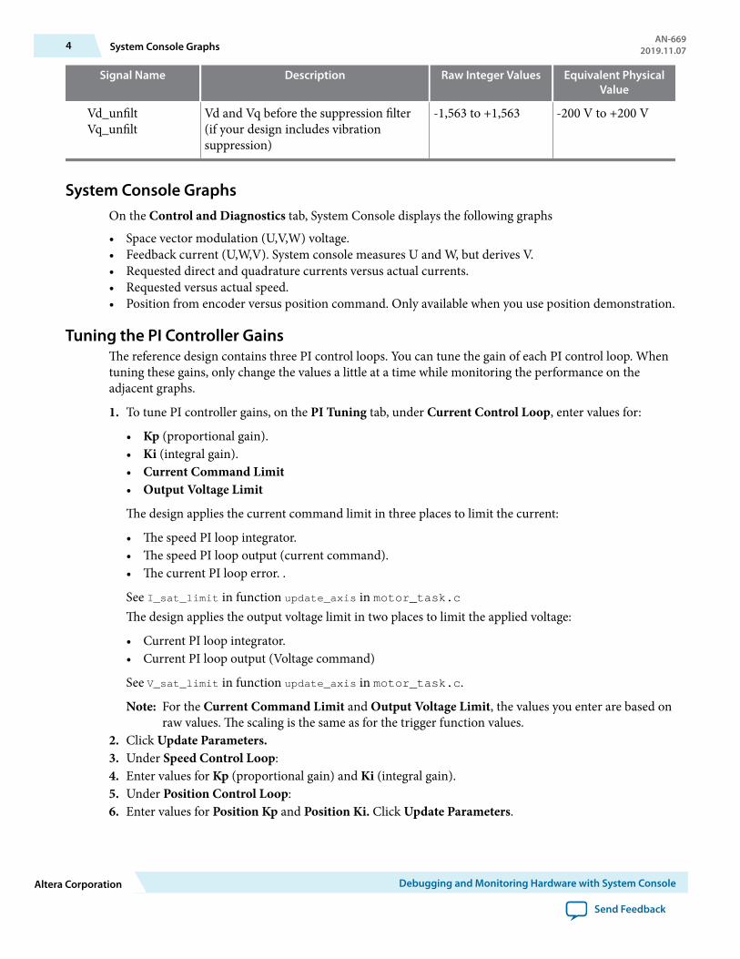
Signal Name Description Raw Integer Values Equivalent PhysicalValue
Vd_unfiltVq_unfilt
Vd and Vq before the suppression filter(if your design includes vibrationsuppression)
-1,563 to +1,563 -200 V to +200 V
System Console GraphsOn the Control and Diagnostics tab, System Console displays the following graphs
• Space vector modulation (U,V,W) voltage.• Feedback current (U,W,V). System console measures U and W, but derives V.• Requested direct and quadrature currents versus actual currents.• Requested versus actual speed.• Position from encoder versus position command. Only available when you use position demonstration.
Tuning the PI Controller GainsThe reference design contains three PI control loops. You can tune the gain of each PI control loop. Whentuning these gains, only change the values a little at a time while monitoring the performance on theadjacent graphs.
1. To tune PI controller gains, on the PI Tuning tab, under Current Control Loop, enter values for:
• Kp (proportional gain).• Ki (integral gain).• Current Command Limit• Output Voltage Limit
The design applies the current command limit in three places to limit the current:
• The speed PI loop integrator.• The speed PI loop output (current command).• The current PI loop error. .
See I_sat_limit in function update_axis in motor_task.cThe design applies the output voltage limit in two places to limit the applied voltage:
• Current PI loop integrator.• Current PI loop output (Voltage command)
See V_sat_limit in function update_axis in motor_task.c.
Note: For the Current Command Limit and Output Voltage Limit, the values you enter are based onraw values. The scaling is the same as for the trigger function values.
2. Click Update Parameters.3. Under Speed Control Loop:4. Enter values for Kp (proportional gain) and Ki (integral gain).5. Under Position Control Loop:6. Enter values for Position Kp and Position Ki. Click Update Parameters.
4 System Console GraphsAN-669
2019.11.07
Altera Corporation Debugging and Monitoring Hardware with System Console
Send Feedback
Related InformationSignals and Raw Versus Physical Values on page 3
Vibration Suppression Tab
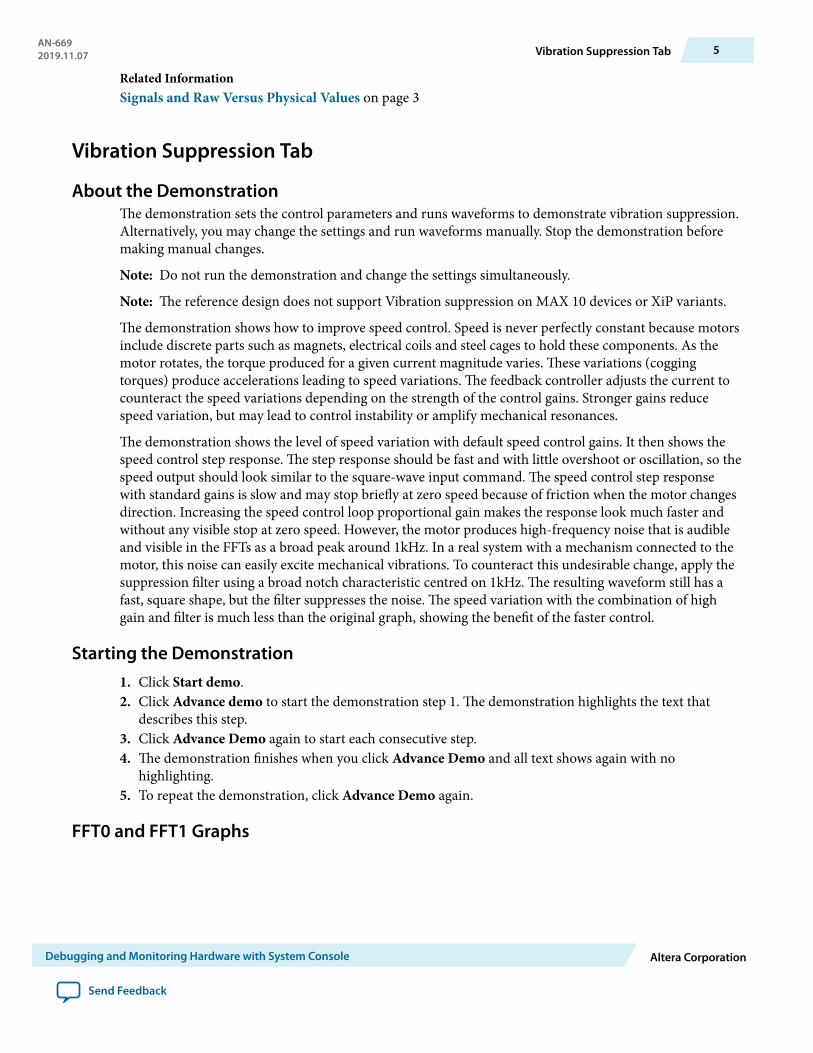
About the DemonstrationThe demonstration sets the control parameters and runs waveforms to demonstrate vibration suppression.Alternatively, you may change the settings and run waveforms manually. Stop the demonstration beforemaking manual changes.
Note: Do not run the demonstration and change the settings simultaneously.
Note: The reference design does not support Vibration suppression on MAX 10 devices or XiP variants.
The demonstration shows how to improve speed control. Speed is never perfectly constant because motorsinclude discrete parts such as magnets, electrical coils and steel cages to hold these components. As themotor rotates, the torque produced for a given current magnitude varies. These variations (coggingtorques) produce accelerations leading to speed variations. The feedback controller adjusts the current tocounteract the speed variations depending on the strength of the control gains. Stronger gains reducespeed variation, but may lead to control instability or amplify mechanical resonances.
The demonstration shows the level of speed variation with default speed control gains. It then shows thespeed control step response. The step response should be fast and with little overshoot or oscillation, so thespeed output should look similar to the square-wave input command. The speed control step responsewith standard gains is slow and may stop briefly at zero speed because of friction when the motor changesdirection. Increasing the speed control loop proportional gain makes the response look much faster andwithout any visible stop at zero speed. However, the motor produces high-frequency noise that is audibleand visible in the FFTs as a broad peak around 1kHz. In a real system with a mechanism connected to themotor, this noise can easily excite mechanical vibrations. To counteract this undesirable change, apply thesuppression filter using a broad notch characteristic centred on 1kHz. The resulting waveform still has afast, square shape, but the filter suppresses the noise. The speed variation with the combination of highgain and filter is much less than the original graph, showing the benefit of the faster control.
Starting the Demonstration1. Click Start demo.2. Click Advance demo to start the demonstration step 1. The demonstration highlights the text that
describes this step.3. Click Advance Demo again to start each consecutive step.4. The demonstration finishes when you click Advance Demo and all text shows again with no
highlighting.5. To repeat the demonstration, click Advance Demo again.
FFT0 and FFT1 Graphs
AN-6692019.11.07 Vibration Suppression Tab 5
Debugging and Monitoring Hardware with System Console Altera Corporation
Send Feedback

On the Vibration Suppression tab, System Console displays the following graphs:
• Input signal to FFT0 against time.• The magnitude of FFT0 against frequency.• Input signal to FFT1 against time.• The magnitude of FFT1 against frequency.
The graphs update at the same time as the graphs on the Control and Diagnostics tab whenever thetrigger function in that tab activates. Within the SoC, the 4,096pt FFT data recalculates after every 64 newdata points. The data sample rate is 16 kHz, thus the FFTs recalculate at 250 Hz.
System Console saves both the time- and frequency-based data to the .csv file that you specify in theControl and Diagnostics tab. You can then verify offline the correctness of the FFT calculation.
The FFT magnitude data is in dB (i.e. 20*log10 absolute value in physical units) similar to a control systemBode plot.
A basic peak detection algorithm enables you to measure particular peaks and develop automatedvibration suppression. For each of the two FFTs, the algorithm finds the maximum magnitude valuebetween two specified frequency limits. Thus, you can search for peaks within a physically relevant rangewithout seeing large FFT magnitudes that often occur at low frequencies. System Console shows the peakswith a cross-hair superimposed on the FFT magnitude graph. It shows the frequency and magnitudevalues below the graph.
Figure 1: Using the Graphs
You can zoom into an area of the graph by clicking and dragging the cursor over that area. To return to theoriginal scaling, right-click on the graph and select Auto Range, Both Axes.'
Setting Up FFT1. On the Vibration Suppression tab, select the FFT signal.2. Select the frequency scale: linear or log.3. Select the peak detection low and high limit frequencies.4. Click Update Limits.
Related InformationSignals and Raw Versus Physical Values on page 3
Setting Up Command WaveformYou can set up the command waveform to generate repeating waveforms that allow you to examine thequality of control.
1. Enter values for the parameters.
Table 2: Command Waveform Parameters
Parameter Value Description
Waveform type Sine, Triangle,Square, Sawtooth
The shape of the repeating waveform.
Period(samples)
2 to 32768 Period of the waveform, in 16 kHz samples. For example, 2000 isequivalent to 8 Hz.
6 Setting Up FFTAN-669
2019.11.07
Altera Corporation Debugging and Monitoring Hardware with System Console
Send Feedback
Parameter Value Description
Positionamplitude
-180 to +180 +/- amplitude of the waveform, if running in position control.Negative values create a 180 degree phase shift.
Speedamplitude(rpm)
-2048 to +2048 +/- amplitude of the waveform, if running in speed control. Negativevalues create a 180 degree phase shift.
On/Off On or Off Switches the waveform on or off. The waveform is superimposed onthe speed or position set points from the General tab.
2. Click Update waveform.
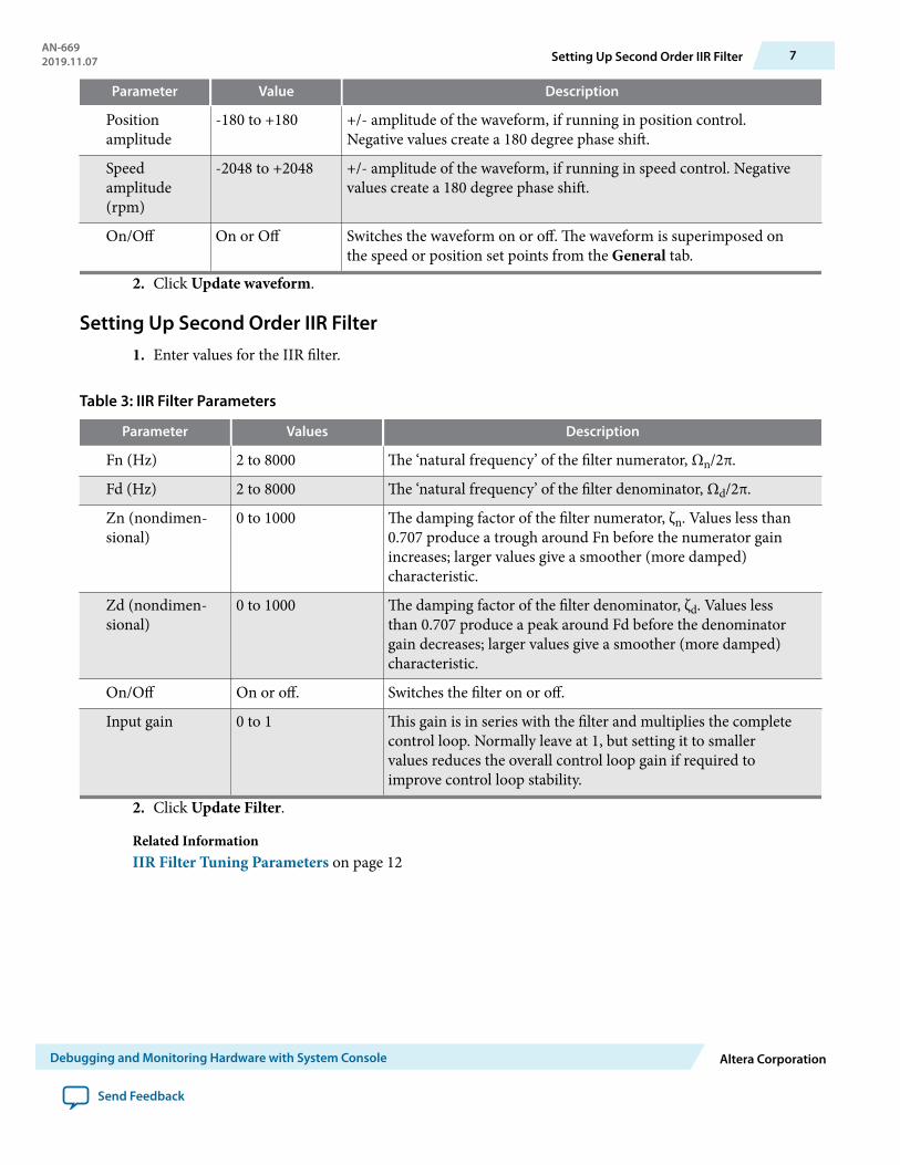
Setting Up Second Order IIR Filter1. Enter values for the IIR filter.
Table 3: IIR Filter Parameters
Parameter Values Description
Fn (Hz) 2 to 8000 The ‘natural frequency’ of the filter numerator, Ωn/2π.
Fd (Hz) 2 to 8000 The ‘natural frequency’ of the filter denominator, Ωd/2π.
Zn (nondimen‐sional)
0 to 1000 The damping factor of the filter numerator, ζn. Values less than0.707 produce a trough around Fn before the numerator gainincreases; larger values give a smoother (more damped)characteristic.
Zd (nondimen‐sional)
0 to 1000 The damping factor of the filter denominator, ζd. Values lessthan 0.707 produce a peak around Fd before the denominatorgain decreases; larger values give a smoother (more damped)characteristic.
On/Off On or off. Switches the filter on or off.
Input gain 0 to 1 This gain is in series with the filter and multiplies the completecontrol loop. Normally leave at 1, but setting it to smallervalues reduces the overall control loop gain if required toimprove control loop stability.
2. Click Update Filter.
Related InformationIIR Filter Tuning Parameters on page 12
AN-6692019.11.07 Setting Up Second Order IIR Filter 7
Debugging and Monitoring Hardware with System Console Altera Corporation
Send Feedback
Functional Description2019.11.07
AN-669 Subscribe Send Feedback
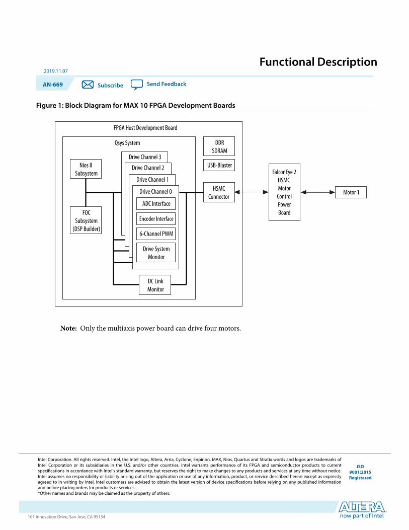
Figure 1: Block Diagram for MAX 10 FPGA Development Boards
Nios II Subsystem
Qsys System
HSMCConnector
FPGA Host Development Board
FOCSubsystem
(DSP Builder)
DC LinkMonitor
Motor 1
ADC Interface
Encoder Interface
6-Channel PWM
Drive SystemMonitor
DDRSDRAM
USB-Blaster
Drive Channel 0
Drive Channel 1
Drive Channel 2
Drive Channel 3
FalconEye 2HSMC Motor
ControlPowerBoard
Note: Only the multiaxis power board can drive four motors.
Intel Corporation. All rights reserved. Intel, the Intel logo, Altera, Arria, Cyclone, Enpirion, MAX, Nios, Quartus and Stratix words and logos are trademarks ofIntel Corporation or its subsidiaries in the U.S. and/or other countries. Intel warrants performance of its FPGA and semiconductor products to currentspecifications in accordance with Intel's standard warranty, but reserves the right to make changes to any products and services at any time without notice.Intel assumes no responsibility or liability arising out of the application or use of any information, product, or service described herein except as expresslyagreed to in writing by Intel. Intel customers are advised to obtain the latest version of device specifications before relying on any published informationand before placing orders for products or services.*Other names and brands may be claimed as the property of others.
ISO9001:2015Registered
www.altera.com101 Innovation Drive, San Jose, CA 95134
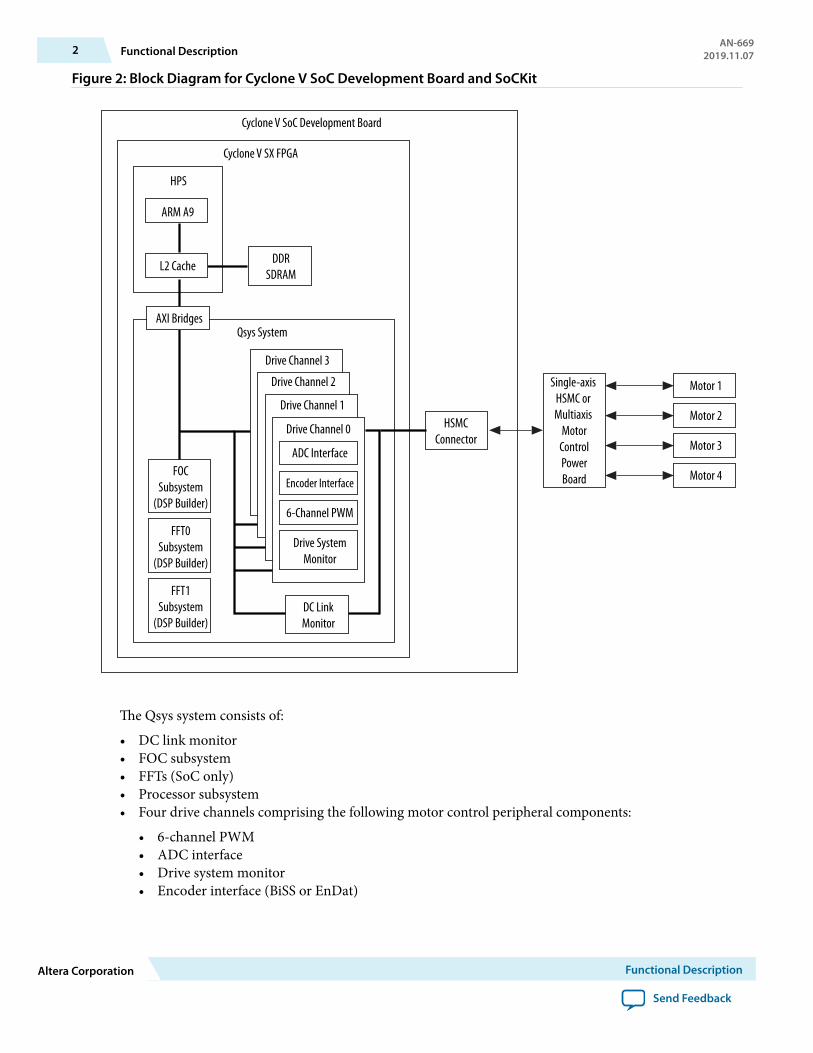
Figure 2: Block Diagram for Cyclone V SoC Development Board and SoCKit
Qsys System
Cyclone V SX FPGA
HSMCConnector
HPS
Cyclone V SoC Development Board
FOCSubsystem
(DSP Builder)
FFT0Subsystem
(DSP Builder)
FFT1Subsystem
(DSP Builder)DC LinkMonitor
ADC Interface
Encoder Interface
6-Channel PWM
Drive SystemMonitor
DDRSDRAM
Drive Channel 0
Drive Channel 1
Drive Channel 2
Drive Channel 3
L2 Cache
ARM A9
AXI Bridges
Motor 1
Motor 2
Motor 3
Motor 4
Single-axis HSMC or Multiaxis
MotorControlPowerBoard
The Qsys system consists of:
• DC link monitor• FOC subsystem• FFTs (SoC only)• Processor subsystem• Four drive channels comprising the following motor control peripheral components:
• 6-channel PWM• ADC interface• Drive system monitor• Encoder interface (BiSS or EnDat)
2 Functional DescriptionAN-669
2019.11.07
Altera Corporation Functional Description
Send Feedback
DC Link MonitorThe DC link monitor comprises:
• Parallel input and output (PIO) for PFC monitor• DC link voltage monitor• DC link current monitor
FOC SubsystemThe Drive-On-Chip Reference Designs use DSP Builder for Intel FPGAs to generate the HDL code forfloating-point and fixed-point implementations of the field-oriented control (FOC) algorithm. The Nios IIprocessor uses this DSP Builder-generated FOC IP as a coprocessor and moves the data between the FOCIP and the peripherals .
Note: Alternatively, the reference design includes software implementations of the FOC algorithm withthe same FOC functionality. You can select which implementation to run using the Debug GUI. Inall FOC implementations, the reference design performs the reverse Clarke transform as part of theSVM function in software.
FOC controls a motor's sinusoidal 3-phase currents in real time to create a smoothly rotating magneticflux pattern, where the frequency of rotation corresponds to the frequency of the sine waves. FOC controlsthe current vector to keep:
• The torque-producing quadrature current, Iq, at 90 degrees to the rotor magnet flux axis• The direct current component, Id, (commanded to be zero) inline with the rotor magnet flux.
The FOC algorithm:
1. Converts the 3-phase feedback current inputs and the rotor position from the encoder into quadratureand direct current components using Clarke and Park transforms.
2. Uses these current components as the inputs to two proportional and integral (PI) controllers runningin parallel to limit the direct current to zero and the quadrature current to the desired torque.
3. Converts the direct and quadrature voltage outputs from the PI controllers back to 3-phase voltageswith inverse Clarke and Park transforms.
The FOC algorithm includes:
• Forward and reverse Clarke and Park transforms• Direct and quadrature current• Proportional integral (PI) control loops• Sine and cosine• Saturate functions
About DSP Builder for Intel FPGAsDSP Builder for Intel FPGAs supports bit-accurate simulation and VHDL generation of the full range offixed-point and floating-point data types available in Simulink*. Floating-point data types give a highdynamic range, avoid arithmetic overflows, and avoid the manual floating- to fixed-point conversion andscaling steps necessary in algorithm development. You can optimize the data types to adjust hardwareusage and calculation latency, and run Simulink simulations to confirm adequate performance.
AN-6692019.11.07 DC Link Monitor 3
Functional Description Altera Corporation
Send Feedback
After you develop the algorithm in Simulink, DSP Builder can automatically generate pipelined HDL thatit targets and optimizes to the chosen FPGA device. You can use this VHDL in a HDL simulator such asModelSim* to verify the generated logic versus Simulink and in the Quartus Prime software to compile thehardware. DSP Builder for Intel FPGAs gives instant feedback of the VHDL's logic utilization andalgorithm latency in automatically generated Simulink reports.
DSP Builder for Intel FPGAs FoldingDSP Builder for Intel FPGAs generates flat parallel models that can receive and process new input dataevery sample time. However, designs which have a much lower sample rate than the FPGA clock rate, suchas this FOC design (16 kHz versus 100 MHz), can use the DSP Builder for Intel FPGAs folding feature totrade off an increase in algorithm latency for a decrease in the used FPGA resources. This feature allowsthe design to use as much hardware parallelism as necessary to reach the target latency with the most costeffective use of FPGA resources without making any changes to the algorithm.
The DSP Builder for Intel FPGAs folding feature reuses physical resources such as multipliers and addersfor different calculations with the VHDL generation automatically handling the complexity of building thetime division multiplexed (TDM) hardware for the particular sample to clock rate ratio.
Figure 3: Unfolded and Folded Hardware Examples
X
X
Unfolded Hardware Transforms to Folded Hardware
Z-1
Z-1
Z-1
+X
AB
C
D
AB
CD
+
DSP Builder Model Resource UsageIntel compared the FOC algorithm as a single precision floating-point model and a model that uses thefolding feature. When you use folding, the model uses fewer logic elements (LEs) and multipliers but hasan increase in latency. In addition, a fixed-point model uses significantly fewer LEs and multipliers and haslower latency than the floating-point model.
Intel compared floating- and fixed-point versions of the FOC algorithm with and without folding. Inaddition, Intel compared using a 26-bit (17-bit mantissa) instead of standard single-precision 32-bit (23-bit mantissa) floating point implementation. 26-bit is a standard type within DSP Builder that takesadvantage of the FPGA architecture to save FPGA resources if this precision is sufficient.
Cyclone V devices use ALMs instead of LEs (one ALM is approximately two LEs plus two registers) andDSP blocks instead of multipliers (one DSP block can implement two 18-bit multipliers or otherfunctions).
4 DSP Builder for Intel FPGAs FoldingAN-669
2019.11.07
Altera Corporation Functional Description
Send Feedback
Table 1: Resource Usage Comparison for Cyclone V Devices
Algorithm Precision (Bits) Folding LogicUsage(ALMs)
DSP Usage AlgorithmLatency (µs)
FOC, floating pointincluding filter, DFf_float_alu_av.slx
32 No 11.5k 31 0.71
FOC, floating pointincluding filter, DFf_float_alu_av.slx
32 Yes 3.9k 4 2.30
FOC, floating pointincluding filter, DFf_float_alu_av.slx
26 No 11k 31 0.70
FOC, floating pointincluding filter, DFf_float_alu_av.slx
26 Yes 3.6k 4 2.34
FOC, fixed point, includingfilter, DFf_fixp16_alu_av.slx
16 No 1.6k 36 0.22
FOC, fixed point, includingfilter, DFf_fixp16_alu_av.slx
16 Yes 2.3k 2 3.31
Table 2: Resource Usage Comparison for MAX 10 Devices
Algorithm Precision (Bits) Folding LogicUsage(LEs)
MultiplierUsage
AlgorithmLatency (µs)
FOC, floating point withoutfilter, DF_float_alu_av.slx
32 No 30k 53 0.52
FOC, floating point withoutfilter, DF_float_alu_av.slx
32 Yes 6.5k 10 1.75
FOC, floating point withoutfilter, DF_float_alu_av.slx
26 No 23k 23 0.47
FOC, floating point withoutfilter, DF_float_alu_av.slx
26 Yes 5.4k 6 1.61
FOC, fixed point, withoutfilter, DF_fixp16_alu_av.slx
16 No 2.2k 12 0.14
FOC, fixed point, withoutfilter, DF_fixp16_alu_av.slx
16 Yes 2.7k 2 2.08
AN-6692019.11.07 DSP Builder Model Resource Usage 5
Functional Description Altera Corporation
Send Feedback
The results show:
• The model with folding uses fewer processing resources but has an increase in latency.• A floating-point model with folding also uses significantly fewer logic resources (LEs/ALMs) than a
model without folding.• The 26-bit floating-point format saves significant resources compared to 32-bit in MAX 10 devices but
proportionally less in Cyclone V SoCs.• The fixed-point algorithms without folding use the fewest logic resources and give the lowest latency.
The reference design implements these FOC configurations:
• Floating-point 26-bit model on MAX 10 devices ; 32-bit on Cyclone V, both with folding.• Fixed-point 16-bit model without folding.
Related InformationGenerating VHDL for the DSP Builder Models for the Drive-On-Chip Reference Designs on page 8
DSP Builder for Intel FPGAs Design GuidelinesUse these design guidelines to reduce FPGA resource usage with folding.
In your design:
• For fixed-point designs use the variable precision support in DSP Builder for Intel FPGAs. Instead ofusing classical 32-bit datapath, investigate the algorithm and reduce the datapath to a dimension closerto the DSP block size.
• For fixed-point datapaths, disable bit growth for adders and subtracters. For example, use 27-bit data-paths on MAX 10 devices. The bit width should provide sufficient dynamic range for handling thevalues in the algorithm.
• Reduce the output of fixed-point multipliers to the same size as the inputs to better integrate in thedatapath.
• Use smaller components when available. For example, pure sin and cos blocks require a rangereduction stage. Use the smaller sin(pi*x) and cos(pi*x).
• Restructure a sin(pi*x) and a cos(pi*x) into a sin(pi*x) and sin(pi*(0.5-x)) to allow folding to reduceresource usage.
• Ensure that the select line of a multiplexer does not use more bits than necessary. For example, for a 2:1multiplexer, the select line should be 1 bit.
DSP Builder for Intel FPGAs Model for the Drive-On-Chip Reference DesignsThe top-level model is a simple dummy testbench with constant inputs of the correct arithmetic types tocontrol hardware generation, which includes the FOC algorithm model.
6 DSP Builder for Intel FPGAs Design GuidelinesAN-669
2019.11.07
Altera Corporation Functional Description
Send Feedback
Figure 4: DSP Builder for Intel FPGAs Model
Motor
PositionSpeed
PositionPI Control
SpeedPI Control
PositionSensor
(Encoder)
CurrentFeedback
PositionFeedback
OutputVoltagePosition
Request
FOCAlgorithm
(DSPBuilderBlocks)
The FOC algorithm comprises the FOC algorithm block and a latch block for implementing the integra‐tors necessary for the PI controllers in the FOC algorithm. DSP Builder for Intel FPGAs implements thelatches outside because of limitations of the folding synthesis.
The reference design includes fixed-point and floating-point models that implement the FOC algorithm.
Each model calls a corresponding .m setup script during initialization to set up the arithmetic precision,folding factor, and target clock speed. The folding factor is set to a large value to minimize resource usage.
Table 3: Default settings in Setup Script
Model Folding Factor Clock Speed (MHz) Input Precision Output Precision
Fixed point 500 100 sfix16En10 sfix32En10
Floating point 500 100 sfix32En10 sfix32En10
The following models generate the FOC block including the Avalon-MM interface:
• DF_float_alu_av.slx for floating-point designs• DF_fixp16_alu_av.slx for fixed-point designs
Verification models stimulate the FOC algorithm using dynamically changing inputs:
• verify_DF_float_alu.slx
• verify_DF_fixp16_alu.slx
Closed-loop simulation models validate that the FOC correctly controls a motor in simulation:
• sim_DF_float_alu.slx
• sim_DF_fixp16_alu.slx
AN-6692019.11.07 DSP Builder for Intel FPGAs Model for the Drive-On-Chip Reference Designs 7
Functional Description Altera Corporation
Send Feedback
A Simulink library model contains the main FOC algorithm code, which the models reference:
• foc_blocks.slx
Generating VHDL for the DSP Builder Models for the Drive-On-Chip ReferenceDesigns
1. Start DSP Builder for Intel FPGAs.2. Change the directory to the ip\dspba.3. If you want a different numeric precision, edit the setup_<Simulink Model>.m file corresponding to the
model before opening it.4. Load the model. Check the status of the orange DSP Builder folding block. If the model includes it,
folding is enabled. If it is removed or commented out, the model does not use folding.5. On the Simulation menu, click Start.
DSP Builder for Intel FPGAs generates the VHDL files in ip\dspba\rtl (for Cyclone V devices) or ip\dspba\rtlmax10 (for MAX 10 devices).
Avalon-MM InterfaceThe Drive-On-Chip Reference Design DSP Builder for Intel FPGAs-generated VHDL has a signalinterface that matches the connections in Simulink. In the DSP Builder for Intel FPGAs models, feedbackcurrents, position feedback, torque command, and gain parameters are all parallel inputs into the systemand voltage commands are parallel outputs.
To allow direct connectivity in Qsys, the top-level DSP Builder for Intel FPGAs design adds blocks toterminate the parallel inputs and outputs and handshaking logic with an Avalon-MM register map.
Figure 5: FOC Model integrated in Simulink with Avalon-MM Register Map
DSP Builder for Intel FPGAs ModelPosition
Torque InputRegister
PI ControlParameter
Input Registers
Filter ParameterInput Registers
TorquePI Control
Flux PIControl
InversePark
Transform
SVM(InverseClarke
Transform)
ParkTransform
ClarkeTransform
Position Input Register
Vq
Vd
Vα
Vβ
Vα
Vβ
Vu
VwVv
Iu
Iw
Iα
Iβ
Iq
Id Feedback CurrentInput Register 2
Feedback CurrentInput Register 1
Voltage Output Register 2
Voltage Output Register 1
Filter
Filter
8 Generating VHDL for the DSP Builder Models for the Drive-On-Chip ReferenceDesigns
AN-6692019.11.07
Altera Corporation Functional Description
Send Feedback
DSP Builder for Intel FPGAs generates a .h file that contains address map information for interfacingwith the DSP Builder for Intel FPGAs model.
To run the DSP Builder for Intel FPGAs model as part of the drive algorithm, a C function passes the datavalues between the processor and DSP Builder for Intel FPGAs. The handshaking logic ensures synchroni‐zation between the software and hardware. The software sets up any changes to hardware parameters suchas PI gains, writes new feedback currents, position feedback and torque command input data beforestarting the DSP Builder for Intel FPGAs calculation. The software then waits for the DSP Builder for IntelFPGAs calculation to finish before reading out the new voltage command data.
The ISR that runs the FOC algorithm calls the C function with an option to switch between software andDSP Builder for Intel FPGAs implementations at runtime.
FFTsFFT0 and FFT1 correspond to the two 4,096pt FFT blocks that the design implements on the SoC forvibration suppression. The design provides two FFTs to enable immediate comparison between the FFTs ofdifferent internal control signals. Each calculates an FFT on the last 4,096 samples input to it. The numberof samples between each new calculation is configurable. The design uses 64 samples between each newcalculation, so each new FFT is based on the same data set as the previous one except for 64 new points.Given the sample rate of 16kHz, the design produces new FFT data sets at 250Hz. Thus vibration detectioncan react quickly, before equipment is damaged.
Figure 6: FFT Overlapping Data Sets
SampledSignal
(16 kHz)
FFT(3)
FFT(2)FFT(1)
4,096 pt
64 pt
Servo FFTsThe design uses two parallel instantiations of the DSP Builder Advanced Blockset servo FFT. The servoFFT is a folded FFT design that uses minimal FPGA resources but sufficient performance for typicalindustrial drive applications.
Table 4: FFT Resource Usage
Device Logic Memory Other
Cyclone V 550 ALMs 29 M9K 2 DSP blocks
AN-6692019.11.07 FFTs 9
Functional Description Altera Corporation
Send Feedback
The processing time with a 100-MHz clock is around 0.6ms including the time to clock data out of the FFTblock again. The processing time for two parallel FFTs is the same. You may choose other FFT implemen‐tations for the FPGA for faster processing times if required, at the expense of FPGA resources.
Running test_servofft.mdl
1. When you run the test_servofft.mdl Simulink model in the project dspba directory,setup_test_servofft.m runs the set up configuration parameters for the FFT and imports sampledmotor current data from the input data for the simulation file (test_servofft_sampledata.csv).
2. DSP Builder generates the HDL code.3. Simulink runs the simulation, using the sampled current data from test_servofft_sampledata.csv as
FFT input.4. analyze_test_servofft.m collects the simulation output and creates some MATLAB plots to verify
correct calculation. It compares the simulated servo FFT output with that from the MATLAB FFT andwith output data collected from servo FFT running in hardware.
Vibration SuppressionThe standard FOC loop has a configurable digital filter to enable you to adjust the loop frequencyresponse, which avoids exciting identified vibrations. An outer control loop analyzes motor feedbacksignals using FFTs to identify any vibrations that may be present. If the design detects vibrations, itautomatically adjusts the control gains in the standard control loop and the filter settings to minimize thevibration. The reference design does not include automatic detection and suppression. For detection useSystem Console; for suppression manually configure the IIR filter.
10 Running test_servofft.mdlAN-669
2019.11.07
Altera Corporation Functional Description
Send Feedback
Figure 7: Control Loop Flow Diagram for Vibration Suppression
4,096 pts250 Hz
CommandWaveform
Control Positionand Velocity
Apply SVM
Apply PWM
SD ADC: 20 MHzBiSS/EnDAT: 10 MHz
Voltage command, 16 kHz
Space vector command, 16 kHz
Transistor switching signals, 50 MHz
Command, 16 kHz
Current demand, 16 kHz
FilterParameters250 Hz
SensorSignals16 kHz
Field-OrientedControl
Measure current, DC voltage,
and postition
Apply FFT
Detect vibration
and tune
IIR filter
Read SensorInterfaces
Apply forwardPark and
Clarke transforms
Apply inverse Park and Clarke transforms
Apply Filter
Control Current
Methods of automatically tuning filter and control gains depend on:
• Knowledge of the mechanical and electrical properties of the mechanisms that the motor drives• The effects of different filter settings on the overall control response
Command WaveformThe command waveform generator provides repeating waveforms. The design uses these waveforms fordeveloping the overall control system including any vibration suppression features. The waveformsgenerate repeatable behavior for given control system settings.
You can choose the waveform shape, period (expressed as a number of 16 kHz samples), and amplitude.
IIR FilterThe design applies an IIR filter to the FOC voltages Vd and Vq before it applies them to the motor.
AN-6692019.11.07 Command Waveform 11
Functional Description Altera Corporation
Send Feedback
The IIR filter is a configurable second-order digital filter, based on the second-order continuous time
transfer function (in Laplace notation):
The design converts the continuous time formulation to a discrete-time formulation using a combinationof the Tustin (bilinear) transformation and frequency prewarping, which ensures that the discrete timeand continuous time filter characteristics match at a specified frequency Ω:
The design applies prewarping to the denominator terms with Ω = Ωd and to the numerator terms with Ω= Ωn, which ensures that the filter preserves the corner frequencies of Ωd and Ωn after the transforma‐tion.
The design applies the IIR filter to the Vd and Vq voltage signals. These signals are the final outputs of thelinear control system before the trigonometric transformation to stator-fixed voltages (Vα and Vβ) and thespace vector modulation (SVM) conversion to transistor gate signals.
The IIR filter is integrated into the FOC algorithm. Different DSP modes use different implementations ofthe FOC algorithm. Each implementation of the FOC algorithm includes a matching implementation ofthe IIR filter.
IIR Filter Tuning Parameters
Table 5: IIR Filter Tuning Parameters
Parameter Description
Ωd Corner frequency (rad/s) above which the denominator response magnitude begins todecrease.
ζd Damping factor that determines the sharpness of the corner at Ωd; ζd < sqrt(0.5) results in afilter response peak (filter resonance) around Ωd, whereas ζd > sqrt(0.5) gives a moregradual (more strongly damped) transition with no peak.
Ωn Corner frequency (rad/s) above which the numerator response magnitude begins toincrease.
ζn Damping factor that determines the sharpness of the corner at Ωn; ζn < sqrt(0.5) results in afilter response trough around Ωn, whereas ζn > sqrt(0.5) gives a more gradual transitionwith no trough.
Use these four parameters to create different filter response shapes. For vibration suppression, use a notchcharacteristic to decrease the system gain only around the frequency of interest. Set Ωn = Ωd and ζn < ζd.The gain at Ωn = Ωd is then equal toζn/ ζd
12 IIR Filter Tuning ParametersAN-669
2019.11.07
Altera Corporation Functional Description
Send Feedback
IIR Filter Examples
Table 6: Exanple IIR Filters
Description Ωd (Hz) Ωn (Hz) ζd(nondimen‐
sional)
ζn(nondimen‐
sional)
Sharp notch with 10x gain reduction at 2kHz
2,000 2,000 0.3 0.03
Wide notch with 10x gain reduction at1 kHz
1,000 1,000 100 10
Figure 8: Bode Plot—Sharp Notch with 10x Gain Reduction at 2 kHz
AN-6692019.11.07 IIR Filter Examples 13
Functional Description Altera Corporation
Send Feedback
Figure 9: Bode Plot, Wide Notch with 10x Gain Reduction at 1 kHz
Vibration DetectionRaw FFT output is a complex-valued array of 4,096 points. The DMA peripheral in the SoC transfers thisdata from the FPGA part of the SoC to processor RAM. Software converts the real and imaginary parts toFFT magnitude (squared) and then applies a basic peak detection algorithm. A peak is the largest FFTmagnitude value between two specified frequency bounds. Peak detection allows you to identify and readpeak values from the FFT magnitude graphs in System Console.
Nios II Subsystem for MAX 10 FPGA Development KitsThe Drive-On-Chip reference design Nios II subsystem comprises the following Qsys components for afully functional processor system with debugging capabilities:
14 Vibration DetectionAN-669
2019.11.07
Altera Corporation Functional Description
Send Feedback
• Nios II fast processor• Floating-point hardware custom instructions 2 (optional)• Tightly coupled instruction and data memory• JTAG master• Performance counters• Clocking and bridge• SDRAM controller• JTAG UART• System console debugging RAM• Debugging dump memory
The ISR uses the tightly coupled memory blocks for code and data to ensure fast predictable executiontime for the motor control algorithm.
The Nios II subsystem uses the JTAG master and debug memories to allow real-time interactions betweenSystem Console and the processor. The reference design uses the System Console debugging RAM to sendcommands and receive status information. The debugging dump memory stores trace data that you candisplay as time graphs in System Console.
Related InformationQsys Interconnect and System Design ComponentsFor more information about these components
Motor Control Peripheral ComponentsThe motor control peripheral components comprise:
• 6-channel pulse width modulator (PWM)• ADC interface• BiSS encoder interface• EnDat encoder interface• Drive system monitor
The reference design puts the motor control peripheral components in a separate Qsys subsystem (DOC_AXIS_Periphs.qsys), which allows you to disable, enable, or add, extra axes.
This section describes the motor control peripheral components and describes specific connectivity issueswhen instancing the motor control suite peripherals in Qsys.
Related InformationMotor Control IP Suite Components for Drive-on-Chip Reference Designs.For more information about the drive system monitor
6-Channel PWMThe 6-channel PWM provides an 8-kHz switching period, and a start pulse every 16 kHz shortly beforethe reversal point of the PWM counter. This pulse goes to the ADC to start capturing data and when theADC finishes it sends an interrupt to the processor. The interrupt output from the first axis and drive0(doc_adc_irq) is connected to the processor. You may leave the interrupt outputs from the other axesunconnected.
AN-6692019.11.07 Motor Control Peripheral Components 15
Functional Description Altera Corporation
Send Feedback
The PWM provides synchronization between multiple PWM instances. To implement this feature thereference design programs the PWMs identically: in Qsys one instance is the master PWM and connectsthe sync_out port to the other PWM sync_in port. For additional instances, continue chaining thesync_out port from the last instance to the next sync_in port. For example:
sync_out (PWM0) to sync_in (PWM1) and sync_out(PWM1) to sync_in(PWM2)
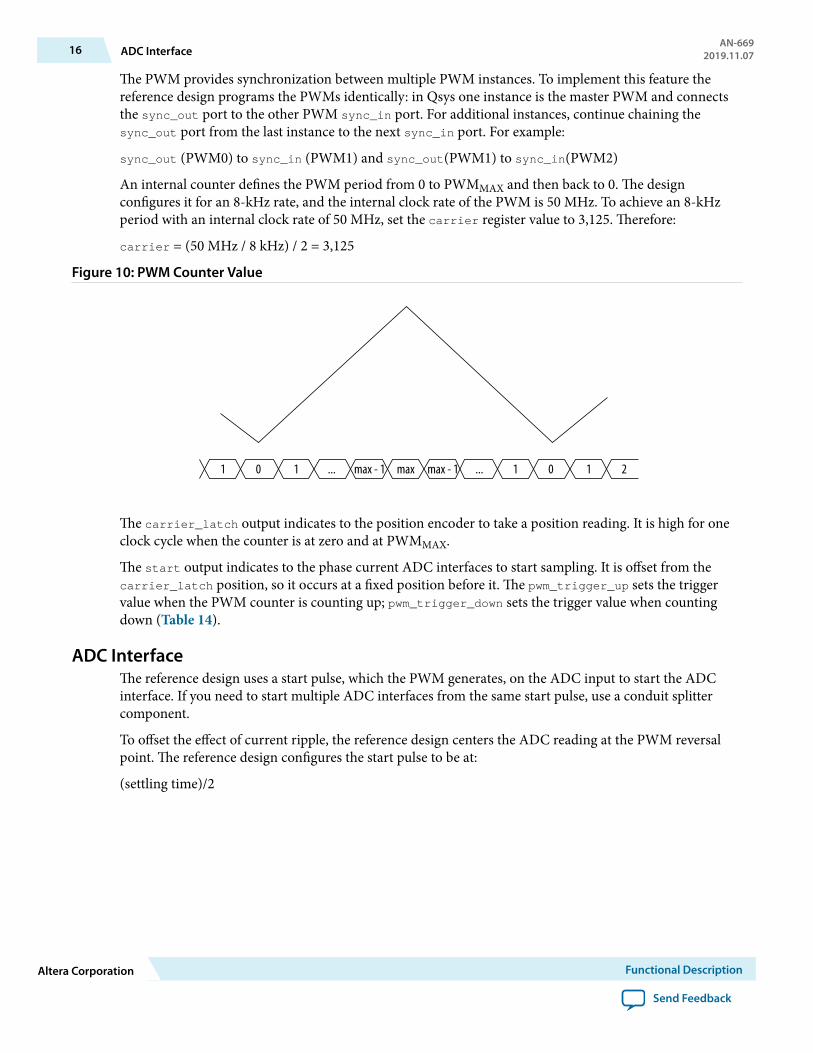
An internal counter defines the PWM period from 0 to PWMMAX and then back to 0. The designconfigures it for an 8-kHz rate, and the internal clock rate of the PWM is 50 MHz. To achieve an 8-kHzperiod with an internal clock rate of 50 MHz, set the carrier register value to 3,125. Therefore:
carrier = (50 MHz / 8 kHz) / 2 = 3,125
Figure 10: PWM Counter Value
1 0 1 ... max - 1 max max - 1 ... 1 0 1 2
The carrier_latch output indicates to the position encoder to take a position reading. It is high for oneclock cycle when the counter is at zero and at PWMMAX.
The start output indicates to the phase current ADC interfaces to start sampling. It is offset from thecarrier_latch position, so it occurs at a fixed position before it. The pwm_trigger_up sets the triggervalue when the PWM counter is counting up; pwm_trigger_down sets the trigger value when countingdown (Table 14).
ADC InterfaceThe reference design uses a start pulse, which the PWM generates, on the ADC input to start the ADCinterface. If you need to start multiple ADC interfaces from the same start pulse, use a conduit splittercomponent.
To offset the effect of current ripple, the reference design centers the ADC reading at the PWM reversalpoint. The reference design configures the start pulse to be at:
(settling time)/2
16 ADC InterfaceAN-669
2019.11.07
Altera Corporation Functional Description
Send Feedback
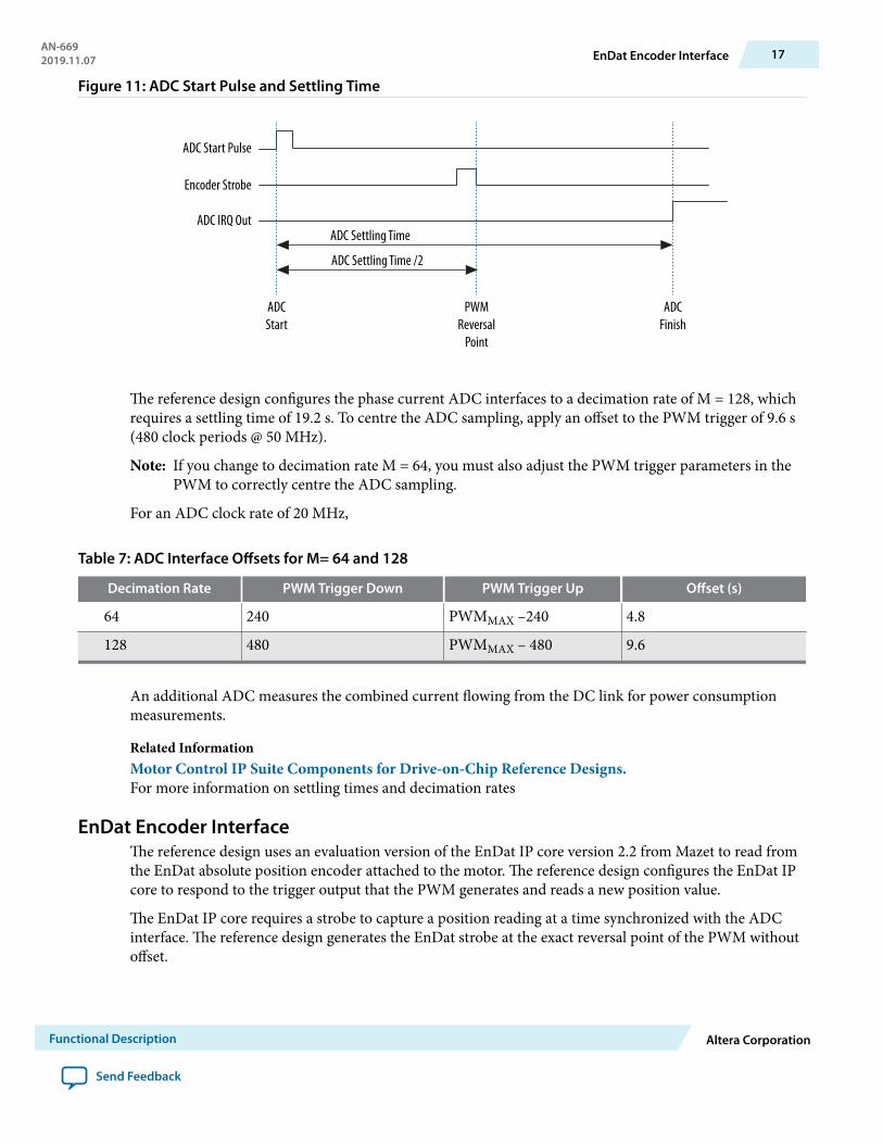
Figure 11: ADC Start Pulse and Settling Time
ADC Start Pulse
Encoder Strobe
ADC IRQ OutADC Settling Time
ADC Settling Time /2
ADCStart
PWMReversal
Point
ADCFinish
The reference design configures the phase current ADC interfaces to a decimation rate of M = 128, whichrequires a settling time of 19.2 s. To centre the ADC sampling, apply an offset to the PWM trigger of 9.6 s(480 clock periods @ 50 MHz).
Note: If you change to decimation rate M = 64, you must also adjust the PWM trigger parameters in thePWM to correctly centre the ADC sampling.
For an ADC clock rate of 20 MHz,
Table 7: ADC Interface Offsets for M= 64 and 128
Decimation Rate PWM Trigger Down PWM Trigger Up Offset (s)
64 240 PWMMAX –240 4.8
128 480 PWMMAX – 480 9.6
An additional ADC measures the combined current flowing from the DC link for power consumptionmeasurements.
Related InformationMotor Control IP Suite Components for Drive-on-Chip Reference Designs.For more information on settling times and decimation rates
EnDat Encoder InterfaceThe reference design uses an evaluation version of the EnDat IP core version 2.2 from Mazet to read fromthe EnDat absolute position encoder attached to the motor. The reference design configures the EnDat IPcore to respond to the trigger output that the PWM generates and reads a new position value.
The EnDat IP core requires a strobe to capture a position reading at a time synchronized with the ADCinterface. The reference design generates the EnDat strobe at the exact reversal point of the PWM withoutoffset.
AN-6692019.11.07 EnDat Encoder Interface 17
Functional Description Altera Corporation
Send Feedback
Note: The reference design connects the strobe signal between the EnDat and PWM in the top levelVerilog HDL design, not in the Qsys system.
Related InformationMazetFor more information about and to purchase a license for the EnDat IP core
BiSS Encoder InterfaceThe reference design uses an evaluation of the BiSS Master IP core version 119 from iC-Haus to read fromthe BiSS absolute position encoder attached to the motor. The reference design configures the BiSS IP coreto respond to the trigger output that the PWM generates and reads a new position value. The BiSS IP corecan communicate with any device complying with the BiSS standard. However, Intel configures thereference design to work with the Hengstler AD36 series of BiSS B encoders.
The ip\biss_OCP directory includes the datasheet for the BiSS Master IP core.
The BiSS IP core requires a strobe to capture a position reading at a time synchronized with the ADCinterface. The reference design generates the BiSS strobe at the exact reversal point of the PWM withoutoffset.
Note: The reference design connects the strobe signal between the BiSS and PWM in the top level VerilogHDL design, not in the Qsys system.
Related InformationiC-Haus BiSS interfaceFor more information about and to license the BiSS Master IP core
18 BiSS Encoder InterfaceAN-669
2019.11.07
Altera Corporation Functional Description
Send Feedback

Motor Control Software2019.11.07
AN-669 Subscribe Send Feedback
The motor control software is in C, runs on an ARM Cortex -A9 in the HPS or Nios II processor, and is intwo sections. The main program covers the initialization, status reporting, and communication functions.The ISR covers the real-time aspects of running the motor control FOC algorithm.
Doxygen generated HTML help files are in the software\CVSX_DS5\DOC_CVSX\source\doxygen orsoftware\source\doxygen directory. Open the index.html file in a browser to view the help files.
Intel Corporation. All rights reserved. Intel, the Intel logo, Altera, Arria, Cyclone, Enpirion, MAX, Nios, Quartus and Stratix words and logos are trademarks ofIntel Corporation or its subsidiaries in the U.S. and/or other countries. Intel warrants performance of its FPGA and semiconductor products to currentspecifications in accordance with Intel's standard warranty, but reserves the right to make changes to any products and services at any time without notice.Intel assumes no responsibility or liability arising out of the application or use of any information, product, or service described herein except as expresslyagreed to in writing by Intel. Intel customers are advised to obtain the latest version of device specifications before relying on any published informationand before placing orders for products or services.*Other names and brands may be claimed as the property of others.
ISO9001:2015Registered
www.altera.com101 Innovation Drive, San Jose, CA 95134
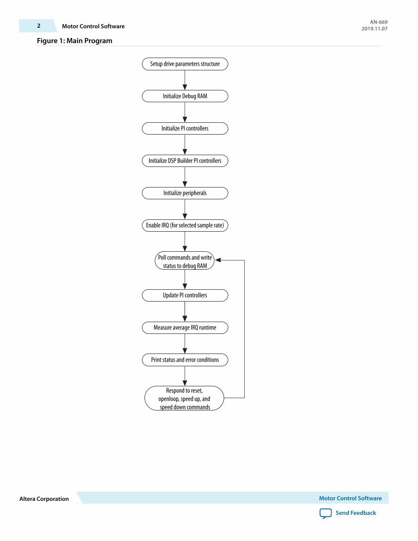
Figure 1: Main Program
Setup drive parameters structure
Initialize Debug RAM
Initialize PI controllers
Initialize DSP Builder PI controllers
Initialize peripherals
Enable IRQ (for selected sample rate)
Poll commands and writestatus to debug RAM
Update PI controllers
Measure average IRQ runtime
Print status and error conditions
Respond to reset, openloop, speed up, and speed down commands
2 Motor Control SoftwareAN-669
2019.11.07
Altera Corporation Motor Control Software
Send Feedback
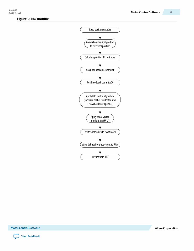
Figure 2: IRQ Routine
Read position encoder
Convert mechanical positionto electrical position
Calculate position PI controller
Calculate speed PI controller
Read feedback current ADC
Apply FOC control algorithm(software or DSP Builder for Intel
FPGAs hardware options)
Apply space vector modulation (SVM)
Write SVM values to PWM block
Write debugging trace values to RAM
Return from IRQ
AN-6692019.11.07 Motor Control Software 3
Motor Control Software Altera Corporation
Send Feedback
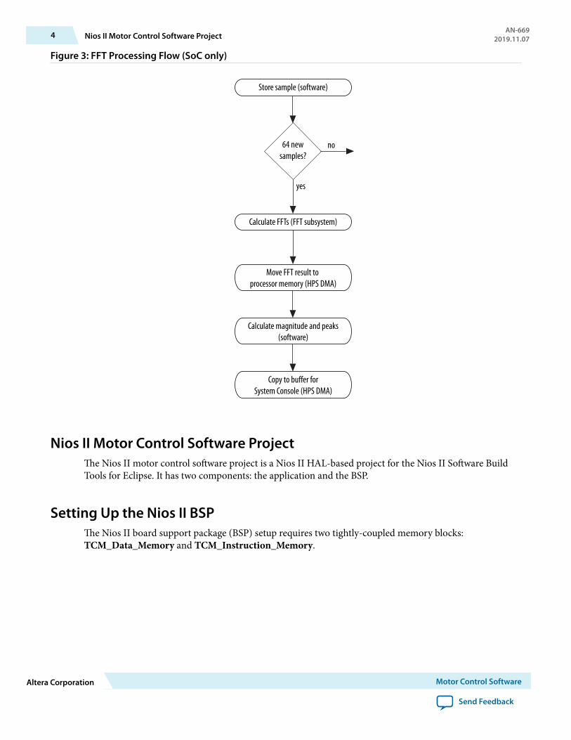
Figure 3: FFT Processing Flow (SoC only)
Store sample (software)
Calculate FFTs (FFT subsystem)
Move FFT result to processor memory (HPS DMA)
Calculate magnitude and peaks(software)
Copy to buffer forSystem Console (HPS DMA)
64 newsamples?
no
yes
Nios II Motor Control Software ProjectThe Nios II motor control software project is a Nios II HAL-based project for the Nios II Software BuildTools for Eclipse. It has two components: the application and the BSP.
Setting Up the Nios II BSPThe Nios II board support package (BSP) setup requires two tightly-coupled memory blocks:TCM_Data_Memory and TCM_Instruction_Memory.
4 Nios II Motor Control Software ProjectAN-669
2019.11.07
Altera Corporation Motor Control Software
Send Feedback
If you make any changes to the default BSP:
• Map .exceptions to TCM_Instruction_Memory (configured in Nios II parameters in System Console)• Map exceptions_stack_memory_region_name to TCM_Data_Memory - size = 1,024• Map interrupt_stack_memory_region_name to TCM_Data_Memory - size = 1,024• Add section .fast_math and map to TCM_Instruction_Memory• Add section .table_data and map to TCM_Data_Memory• Add section .drive_data and map to TCM_Data_Memory
SoC HPS Motor Control Software ProjectThe SoC HPS motor control software project is a executable makefile project for the Altera SoC EmbeddedDesign Suite. The single project contains both the application source and the μC/OS-II source. You canload this standalone application from DS-5 or using U-boot from an SD card.
Note: You may use the μC/OS-II source only for this reference design. If you wish to use the design thatincludes the C/OS-II in your production design, you must license μC/OS-II from Intel partnerMicrium who develop and support the BSP.
Intel provides DS-5 debug script that first loads and runs the preloader, then loads and runs the applica‐tion to a breakpoint at main(). Execution can continue from this point or you can set further breakpointsor configure memory watch windows.
Building the HPS PreloaderIntel provides prebuilt preloader image in the software\spl_bsp\uboot-socfpga\spl directory. Only buildthe preloader if you change the HPS hardware settings.
1. Delete the existing \software\spl-bsp directory to remove the old preloader.2. Run the bsp-editor in the \software directory to ensure that the preloader generate in the correct
directory, so the software Makefile can find it when building the HPS software. The watchdog timermust be disabled in the bsp-editor (turn off WATCHDOG_ENABLE).
Related InformationPreloader User Guide in the SoC EDS User Guide
SoC HPS Execute-in-Place (XiP) VariantThe DOC_FE2H_CVSX_XiP variant is an example of a minimal motor control project for Cyclone VSoCs requiring no external memory. Execute-in-Place (XiP) refers to executing the application directlyfrom flash memory (quad serial peripheral interface (QSPI) in this case). If the code footprint is smallenough to fit entirely in the L2 cache, performance is similar to that achieved with external DDR memoryand L2 cache. The variant uses on-chip RAM (OCRAM) for data storage. You may implement additionalmemory in the FPGA but do not use it for frequently accessed data. Accesses to this memory incur thelatency through the HPS2FPGA bridges. The XiP variant uses FPGA memory for debug data to be sharedwith the System Console debug GUI.
AN-6692019.11.07 SoC HPS Motor Control Software Project 5
Motor Control Software Altera Corporation
Send Feedback
Building the Preloader for XiPIntel provides prebuilt preloader image in the software\spl_bsp\uboot-socfpga\spl directory. Onlyrebuild the preloader if you change the XiP hardware project.
1. Configure the preloader for XiP in the bsp-editor:a. Turn off BOOT_FROM_SDMMCb. Turn on BOOT_FROM_QSPIc. Turn on SKIP_SDRAMd. Turn off WATCHDOG_ENABLE (unless the application is modified to pet the watchdog)e. Turn off SDRAM_SCRUBBINGf. Turn off SDRAM_SCRUB_REMAIN_REGIONg. Turn off HARDWARE_DIAGNOSTIC
2. Generate the preloader.3. Compile the preloader (make all).4. In include/configs/socfpga_common.h, search for the following macros and #define or #undef:
#define CONFIG_SPL_SPI_XIP
#define CONFIG_SPL_SPI_XIP_ADDR 0xFFA40040
#undef CONFIG_USE_IRQ5. Compile the preloader again (make).
Related InformationPreloader User Guide in the SoC EDS User Guide
Building the Application for XiPThe XiP application is an executable makefile project that you can build in DS-5. The steps required toimport the project into DS-5 and build the application are similar to those for the DOC_CVSX variant.
Programming the QSPI FLASH With the XiP Preloader and ApplicationYou must set the BOOTSEL jumpers on the Cyclone V SoC development board to boot from QSPI asBOOTSEL[2:0] left, left, left..
1. Turn off then turn on the power to the board.2. Open the quartus_hps utility in a SoC EDS Command Shell.3. Program the preloader:
quartus_hps -c 1 -o PV --boot=0 preloader-mkpimage.bin4. Program the application:
quartus_hps -c 1 -o PV -a 0x40000 --boot=0 doc_xip-mkimage.bin
If the command fails the first time because the HPS boots from the existing QSPI contents, try again.
XiP Application Debugging ScriptIntel provide a debug script that allows you to debug the XiP application while running from QSPI flash.The script runs the preloader and then the application to a breakpoint at main(). Execution can continuefrom this point or you can set further breakpoints or configure memory watch windows.If the you boot
6 Building the Preloader for XiPAN-669
2019.11.07
Altera Corporation Motor Control Software
Send Feedback

the design from QSPI, BOOTSEL[2:0] is set to left, left, left. If the you run the design from DS5,BOOTSEL[2:0] is set to left, right, right.
AN-6692019.11.07 XiP Application Debugging Script 7
Motor Control Software Altera Corporation
Send Feedback
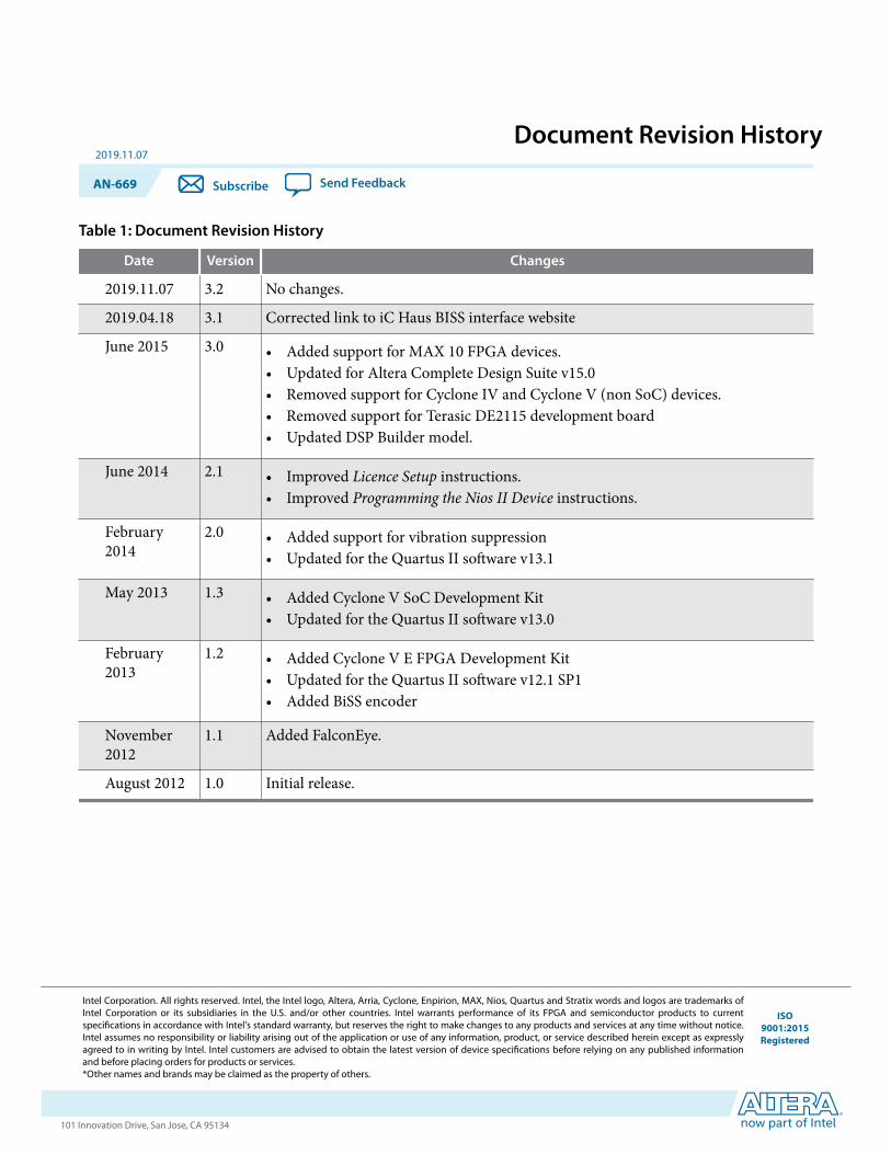
Document Revision History2019.11.07
AN-669 Subscribe Send Feedback
Table 1: Document Revision History
Date Version Changes
2019.11.07 3.2 No changes.
2019.04.18 3.1 Corrected link to iC Haus BISS interface website
June 2015 3.0 • Added support for MAX 10 FPGA devices.• Updated for Altera Complete Design Suite v15.0• Removed support for Cyclone IV and Cyclone V (non SoC) devices.• Removed support for Terasic DE2115 development board• Updated DSP Builder model.
June 2014 2.1 • Improved Licence Setup instructions.• Improved Programming the Nios II Device instructions.
February2014
2.0 • Added support for vibration suppression• Updated for the Quartus II software v13.1
May 2013 1.3 • Added Cyclone V SoC Development Kit• Updated for the Quartus II software v13.0
February2013
1.2 • Added Cyclone V E FPGA Development Kit• Updated for the Quartus II software v12.1 SP1• Added BiSS encoder
November2012
1.1 Added FalconEye.
August 2012 1.0 Initial release.
Intel Corporation. All rights reserved. Intel, the Intel logo, Altera, Arria, Cyclone, Enpirion, MAX, Nios, Quartus and Stratix words and logos are trademarks ofIntel Corporation or its subsidiaries in the U.S. and/or other countries. Intel warrants performance of its FPGA and semiconductor products to currentspecifications in accordance with Intel's standard warranty, but reserves the right to make changes to any products and services at any time without notice.Intel assumes no responsibility or liability arising out of the application or use of any information, product, or service described herein except as expresslyagreed to in writing by Intel. Intel customers are advised to obtain the latest version of device specifications before relying on any published informationand before placing orders for products or services.*Other names and brands may be claimed as the property of others.
ISO9001:2015Registered
www.altera.com101 Innovation Drive, San Jose, CA 95134