Dramatic Reduction of Surface Recombination by in Situ...
6
Published: May 20, 2011 r2011 American Chemical Society 2527 dx.doi.org/10.1021/nl201179n | Nano Lett. 2011, 11, 2527–2532 LETTER pubs.acs.org/NanoLett Dramatic Reduction of Surface Recombination by in Situ Surface Passivation of Silicon Nanowires Yaping Dan, † Kwanyong Seo, † Kuniharu Takei, ‡ Jhim H. Meza, † Ali Javey, ‡ and Kenneth B. Crozier* ,† † School of Engineering and Applied Sciences, Harvard University, Cambridge, Massachusetts 02138, United States ‡ Department of Electrical Engineering and Computer Sciences, University of California, Berkeley, California 94720, United States b S Supporting Information C onsiderable interest exists for nanowire-based solar cells 2,8,1518 because of their potential to achieve high energy conversion efficiency at low cost. However, due to the large surface-to- volume ratio, nanowires have a high surface recombination rate. This shortens the carrier lifetime by 45 orders of magnitude, 9 resulting in the efficiency of nanowire solar cells usually only a few percent. 7,8,10,11 The surface passivation of planar optoelec- tronics is a technology that was developed over the course of decades. 19,20 Nanowire surface passivation, however, is an even more challenging task due to their small size and the fact that multiple facets with different crystalline orientation are exposed. In this Letter, we demonstrate a highly effective means for surface passivation of silicon nanowires, using a thin layer of amorphous silicon formed in situ during nanowire growth. Excitingly, the experimental results obtained by near-field scanning photocur- rent microscopy indicate a ∼100-fold reduction in surface re- combination. The quenched surface recombination prolongs the carrier lifetime and consequently increases photosensitivity or energy conversion efficiency when the nanowires are used as photodetectors or solar cells. Experimental measurements in- dicate a ∼90-fold increase in the photosensitivity of passivated nanowires, as compared to unpassivated ones. This has major implications for solar energy conversion devices. Images of transmission electron microscopy (TEM) and energy dispersive X-ray spectroscopy show that the nanowires have a single-crystalline core and a ∼10 nm thick amorphous silicon (a-Si) shell (Figure 1). The coreshell silicon nanowires (SiNWs) are mostly 4060 μm long and 5090 nm in diameter. The amorphous shell is formed in situ during the nanowire synthesis in the Au-catalyzed vaporliquidsolid (VLS) process that has been widely used for the growth of SiNWs without shells 2123 (see Figure S1 in the Supporting Information for possible growth mechanisms of the amorphous shell). The coreshell nanowires are p-type, confirmed by the result of transimpedance measurement shown in the inset of Figure 2a. The boron doping concentration in the SiNW is estimated to be ∼10 18 cm 3 based on four-probe measurements. To quantify the effect of surface passivation in our coreshell nanowires, we extract the surface recombination velocity S by the following equation (see Figure S2 in the Supporting Infor- mation) 1 τ eff ¼ 1 τ b þ 4S φ ð1Þ where τ eff is the effective carrier lifetime, φ the nanowire diameter, and τ b the carrier lifetime in bulk Si of the same impurity concentration. The left side of the equation is the effective recombination rate which is equal to the addition of bulk (first term on right side) and surface recombination rate (last term on right side). While the nanowire diameter is measured Received: April 8, 2011 Revised: May 11, 2011 ABSTRACT: Nanowires have unique optical properties 14 and are considered as important building blocks for energy harvest- ing applications such as solar cells. 2,58 However, due to their large surface-to-volume ratios, the recombination of charge carriers through surface states reduces the carrier diffusion lengths in nanowires a few orders of magnitude, 9 often resulting in the low efficiency (a few percent or less) of nanowire-based solar cells. 7,8,10,11 Reducing the recombination by surface passi- vation is crucial for the realization of high-performance nanosized optoelectronic devices but remains largely unexplored. 7,1214 Here we show that a thin layer of amorphous silicon (a-Si) coated on a single-crystalline silicon nanowire, forming a coreshell structure in situ in the vaporliquidsolid process, reduces the surface recombination nearly 2 orders of magnitude. Under illumination of modulated light, we measure a greater than 90-fold improvement in the photosensitivity of individual coreshell nanowires, compared to regular nanowires without shell. Simulations of the optical absorption of the nanowires indicate that the strong absorption of the a-Si shell contributes to this effect, but we conclude that the effect is mainly due to the enhanced carrier lifetime by surface passivation. KEYWORDS: Silicon nanowire, surface passivation, scanning photocurrent microscopy, solar cell
Transcript of Dramatic Reduction of Surface Recombination by in Situ...
Published: May 20, 2011
r 2011 American Chemical Society 2527 dx.doi.org/10.1021/nl201179n |Nano Lett. 2011, 11, 2527–2532
LETTER
pubs.acs.org/NanoLett
Dramatic Reduction of Surface Recombination by in Situ SurfacePassivation of Silicon NanowiresYaping Dan,† Kwanyong Seo,† Kuniharu Takei,‡ Jhim H. Meza,† Ali Javey,‡ and Kenneth B. Crozier*,†
†School of Engineering and Applied Sciences, Harvard University, Cambridge, Massachusetts 02138, United States‡Department of Electrical Engineering and Computer Sciences, University of California, Berkeley, California 94720, United States
bS Supporting Information
Considerable interest exists for nanowire-based solar cells2,8,15�18
because of their potential to achieve high energy conversionefficiency at low cost. However, due to the large surface-to-volume ratio, nanowires have a high surface recombination rate.This shortens the carrier lifetime by 4�5 orders of magnitude,9
resulting in the efficiency of nanowire solar cells usually only afew percent.7,8,10,11 The surface passivation of planar optoelec-tronics is a technology that was developed over the course ofdecades.19,20 Nanowire surface passivation, however, is an evenmore challenging task due to their small size and the fact thatmultiple facets with different crystalline orientation are exposed.In this Letter, we demonstrate a highly effective means for surfacepassivation of silicon nanowires, using a thin layer of amorphoussilicon formed in situ during nanowire growth. Excitingly, theexperimental results obtained by near-field scanning photocur-rent microscopy indicate a ∼100-fold reduction in surface re-combination. The quenched surface recombination prolongs thecarrier lifetime and consequently increases photosensitivity orenergy conversion efficiency when the nanowires are used asphotodetectors or solar cells. Experimental measurements in-dicate a ∼90-fold increase in the photosensitivity of passivatednanowires, as compared to unpassivated ones. This has majorimplications for solar energy conversion devices.
Images of transmission electron microscopy (TEM) andenergy dispersive X-ray spectroscopy show that the nanowireshave a single-crystalline core and a ∼10 nm thick amorphoussilicon (a-Si) shell (Figure 1). The core�shell silicon nanowires
(SiNWs) are mostly 40�60 μm long and 50�90 nm in diameter.The amorphous shell is formed in situ during the nanowiresynthesis in the Au-catalyzed vapor�liquid�solid (VLS) processthat has been widely used for the growth of SiNWs withoutshells21�23 (see Figure S1 in the Supporting Information forpossible growth mechanisms of the amorphous shell). Thecore�shell nanowires are p-type, confirmed by the result oftransimpedance measurement shown in the inset of Figure 2a.The boron doping concentration in the SiNW is estimated to be∼1018 cm�3 based on four-probe measurements.
To quantify the effect of surface passivation in our core�shellnanowires, we extract the surface recombination velocity S by thefollowing equation (see Figure S2 in the Supporting Infor-mation)
1τeff
¼ 1τb
þ 4Sφ
ð1Þ
where τeff is the effective carrier lifetime, φ the nanowirediameter, and τb the carrier lifetime in bulk Si of the sameimpurity concentration. The left side of the equation is theeffective recombination rate which is equal to the addition of bulk(first term on right side) and surface recombination rate (lastterm on right side). While the nanowire diameter is measured
Received: April 8, 2011Revised: May 11, 2011
ABSTRACT:Nanowires have unique optical properties1�4 andare considered as important building blocks for energy harvest-ing applications such as solar cells.2,5�8 However, due to theirlarge surface-to-volume ratios, the recombination of chargecarriers through surface states reduces the carrier diffusionlengths in nanowires a few orders of magnitude,9 often resultingin the low efficiency (a few percent or less) of nanowire-basedsolar cells.7,8,10,11 Reducing the recombination by surface passi-vation is crucial for the realization of high-performance nanosized optoelectronic devices but remains largely unexplored.7,12�14
Here we show that a thin layer of amorphous silicon (a-Si) coated on a single-crystalline silicon nanowire, forming a core�shellstructure in situ in the vapor�liquid�solid process, reduces the surface recombination nearly 2 orders of magnitude. Underillumination of modulated light, we measure a greater than 90-fold improvement in the photosensitivity of individual core�shellnanowires, compared to regular nanowires without shell. Simulations of the optical absorption of the nanowires indicate that thestrong absorption of the a-Si shell contributes to this effect, but we conclude that the effect is mainly due to the enhanced carrierlifetime by surface passivation.
KEYWORDS: Silicon nanowire, surface passivation, scanning photocurrent microscopy, solar cell

2528 dx.doi.org/10.1021/nl201179n |Nano Lett. 2011, 11, 2527–2532
Nano Letters LETTER
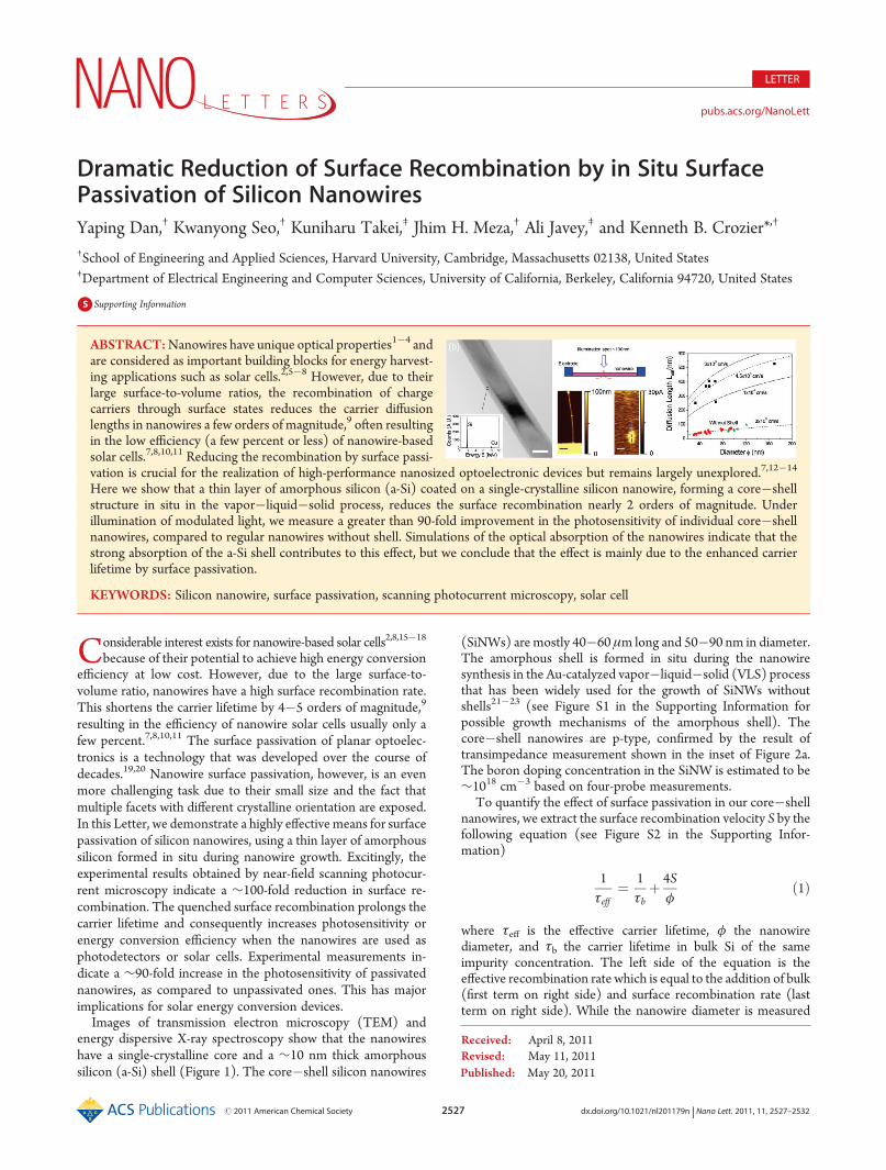
directly by atomic force microscopy (AFM), we obtain theeffective lifetime τeff from the minority diffusion length Ldiff,since the two are related by Ldiff = (Dτeff)
1/2 where D is thediffusion coefficient. To find Ldiff, an electrically neutral region inthe nanowire is created by making two Schottky contacts to the
wire, as shown in Figure 2b. Under both positive and negativebias, one of the two Schottky barriers is reverse biased (black linein Figure 2a). The majority of the applied voltage drops over thereverse biased barrier, with only a negligible part dropped overthe nanowire. A ∼100 nm illumination spot from a near-field
Figure 1. Transmission electron microscope (TEM) images of a core�shell silicon nanowire. (a) High-resolution TEM image, showing that the core issingle-crystalline while the shell is amorphous. Scale bar, 3 nm. (b) TEM image, showing that amorphous shell is ∼10 nm thick and crystalline core is∼40 nm in diameter. Inset: energy dispersive X-ray spectroscopy (EDS) indicates that the amorphous shell is silicon. Scale bar, 30 nm.
Figure 2. Current�voltage characteristics and scanning photocurrent microscopy (SPCM) of core�shell silicon nanowires. The nanowires areintentionally contacted with two Schottky barriers. (a) I�Vmeasurement (dark current, black curve) shows that, under positive or negative voltage, onebarrier is always under reverse bias. I�V measurement with illumination (red curve) is obtained with white light from a microscope lamp. Inset:transimpedance measurement, indicating that nanowire is p-type. (b) Conceptual illustration of method for measuring carrier diffusion lengths.(c) Nanowire topography, obtained by AFM functionality of near-field scanning optical microscope. Scale bar, 1 μm. (d) Photocurrent map, recordedsimultaneously with topographic image. Scale bar, 1 μm. (e) Photocurrent current profiles along nanowire axis (blue dashed line of panel d) for differentvoltages applied to nanowire. Plotted in logarithmic scale, slope of photocurrent vs distance curve does not change with bias voltage, indicating that theexcited charge carriers are diffusive. Larger value of illumination spot location corresponds to it being closer to Schottky contact. (f) At conditions similarto (e), photocurrent profiles along axes of nanowires with diameters of 190, 77, and 51 nm.
2529 dx.doi.org/10.1021/nl201179n |Nano Lett. 2011, 11, 2527–2532
Nano Letters LETTER
scanning optical microscopy (NSOM) tip is used to locallygenerate excess minority carriers in this quasi-neutral region.These carriers diffuse and recombine in the absence of an ex-ternal electric field, leading to the exponential decay in theirpopulation. Only a portion of the excessminority carriers generatedby the illumination spot therefore reaches the reverse biasedbarrier and are collected as photocurrent. From Figure 2b, it canbe seen that photocurrent will increase exponentially as thedistance between the illumination spot and the barrier decreases.We extract the diffusion length Ldiff from this exponential relation-ship between the photocurrent and the illumination spot location.
As discussed, the ∼100 nm illumination spot is created byfocusing a laser beam into a near-field scanning optical micro-scope (NSOM) tip.24�26 This tip is raster scanned over thenanowire in contact mode, enabling the topography (i.e., AFMimage) and photocurrent map to be simultaneously obtained, asshown in panels c and d of Figure 2, respectively. The bright spotin Figure 2d corresponds to the large photocurrents occurringnear the reverse biased Schottky barrier (bottom electrode ofFigure 2c). The photocurrent decays exponentially as the illumina-tion spot moves away from the barrier along the nanowire axis(Figure 2e). From the decay rate, the diffusion length of the77 nm diameter core�shell wire is found to be 410 nm. Variation inthe external voltage modulates the depletion region of the Schottkybarrier and changes the carrier collection efficiency as well as theabsolute value of photocurrent. However, the photocurrent decayslope, and hence the diffusion length, remain constant at differentvoltages (Figure 2e), because the external voltage does not affectthe diffusive nature of excess carriers in the neutral region.Accordingto eq 1, smaller nanowires have larger surface recombination rates,leading to shorter diffusion lengths, as observed in Figure 2f.
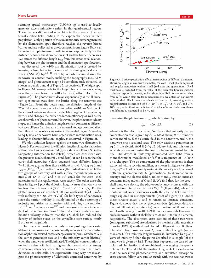
We plot diffusion lengths against the nanowire diameters inFigure 3. For comparison, the diffusion lengths of regular nanowireswithout shell are also measured (green stars, see Figure S3 in theSupporting Information for details), which are consistent withthe previous results from ref 9 (red dots). It can be seen that thecore�shell nanowires (black squares) have diffusion lengths7�11 times greater than those without a shell. Using eq 1 andLdiff = (Dτeff)
1/2, we find two curves (the dashed lines) that fit thetwo groups of data very well with surface recombination veloc-ities S of 4.5 � 103 and 3 � 105 cm/s for the core�shellnanowires and the regular ones, respectively. The other two solidlines in Figure 3 plot the diffusion length versus diameter curvesfor two other choices of S (3 � 103 and 1 � 104 cm/s). For theplotted curves, we use a constant diffusion coefficientD (=4.8 cm2/swith mobility μ ∼200 cm2/(V s)) for both types of nanowires,since the carrier mobility is mainly limited by the scattering ofmajority impurities for nanowires with a doping concentration∼1018 cm�3 as in our case9,27 and therefore is largely indepen-dent of the surface scattering.9 The reduction in surface recom-bination velocity indicates that the a-Si shell has reduced thedensity of surface states on the crystalline core surface nearly2 orders of magnitude.
The quenched surface recombination prolongs the carrierlifetime in nanowires and consequently increases the concentra-tion of photon-excited excess charge carriers (Δn=GτwhereG isthe carrier generation rate and τ the minority carrier lifetime)when the nanowires are illuminated. The higher concentration ofexcited carriers will lead to higher photosensitivity or energyconversion efficiency when the nanowires are used as photo-detectors or solar cells. For experimental simplicity, we investi-gate the photosensitivity of Ohmically contacted nanowires by
measuring the photocurrent Iph which is given by
Iph ¼ eΔnμEA ð2Þwhere e is the electron charge, Δn the excited minority carrierconcentration that is given by Δn = Gτ as above, μ the minoritycarrier mobility, E the electric field in the nanowire, and A thenanowire cross-sectional area. The only extrinsic parameter ineq 2 is the electric field E (=Vin/L, Figure 4a), and this can beaccurately measured using the four probe measurement techni-que. The device is uniformly illuminated with light from amonochromator modulated on/off at a frequency of 1.8 kHzby a chopper. The ac component of the photocurrent is thenextracted with a lock-in amplifier, as shown in Figure 4a. How-ever, eq 2 will not necessarily maintain its linearity as a function ofboth the generation rate G (proportional to illumination in-tensity) and the electric field E, unless τ and μ remain intrinsicconstants independent of G and E. We find that, for the core�shell nanowire device, the photoconductance is linear with theillumination intensity up to ∼25 W/m2 (Figure 4b), while thephotocurrent linearly increases with the electric field over therange explored in our experiments (inset of Figure 4b). Underthese circumstances, τ and μ remain as intrinsic constants.Figure 4c shows that the ac photosensitivity (photoconductivityper unit illumination intensity) as a function of illuminationwavelength ranging from 400 to 900 nm for a core�shell nanowireand a nanowire without shell that are 90 and 130 nm in diameter,respectively. The absorption cross sections of these two wires(on a quartz substrate) are calculated by the finite difference timedomain (FDTD) method and plotted in Figure 4c as solid lines.The absorption cross sections Ac have units of length (ratherthan area). If an infinitely long nanowire is illuminated by a planewave of intensity I, then the power absorbed in a length l of thenanowire is given by IAcl. These lines represent the case of un-polarized illumination and are obtained by averaging the spectraobtained for TE and TM illumination (Figure 4a). It can be seenthat the measured photosensitivity and simulated absorptioncross section follow very similar trends with the two nanowires
Figure 3. Surface passivation effects in nanowires of different diameters.Diffusion length vs nanowire diameter, for core�shell (black squares)and regular nanowires without shell (red dots and green stars). Shellthickness is excluded from the value of the diameter because carriersmainly transport in the core, as data show later. Red dots represent datafrom ref 9. Green stars are from measurements we obtain on nanowireswithout shell. Black lines are calculated from eq 1, assuming surfacerecombination velocities S of 3 � 105, 1 � 104, 4.5 � 103, and 3 �103 cm/s, with diffusion coefficient D of 4.8 cm2/s and bulk recombina-tion lifetime τb extracted to be ∼2 ns.

2530 dx.doi.org/10.1021/nl201179n |Nano Lett. 2011, 11, 2527–2532
Nano Letters LETTER
each having one or more peaks due to leaky mode resonances.28,29
These modes can be found by solving Maxwell’s equations atappropriate boundary conditions for classical optical fiber
waveguides, as described previously.28 Each of the leaky modescan be characterized by an azimuthal mode number, m, and aradial order number, n. In this way, the modes can be termed as
Figure 4. Diagram of experimental setup andmeasured ac photosensitivity spectra. (a) A four point probemeasurement technique is used, withVs beingthe power supply voltage and Vin the measured voltage. Bottom right: nanowire cross section is shown together with definitions of TE and TMillumination. (b) Photoconductance of a core�shell nanowire at different illumination intensities. Inset: photocurrent linearly increases with the biasVin.(c)Measured photosensitivity vs wavelength for a core�shell nanowire (black squares) and a nanowire without shell (red dots). The photosensitivity forthe nanowire without shell has been magnified 50-fold for comparison purposes. The core�shell SiNW has a core diameter of ∼70 nm, and an outerdiameter of ∼90 nm. The nanowire without shell is 130 nm in diameter. FDTD-simulated absorption cross section is plotted for the core�shellnanowire (black line) and the nanowire without shell (red line). (d) Simulated electric field intensity (E2, normalized to incident illumination) of leakymodes for TM illumination. The nanowires are on quartz substrates. The outer circle is the wire�air interface while the inner circle is the interfacebetween a-Si and sc-Si. Upper plot is for the core�shell nanowire. Middle and lower plots are for the regular nanowire without a shell.
Figure 5. Absorption cross section and carrier transport model of the core�shell nanowire. (a) Simulated absorption cross section vs wavelength for thecore�shell nanowire in Figure 4c. Total absorption cross section, i.e., of core and shell, is plotted as a red curve. Absorption cross section of core isplotted as a black curve. (b) Charge carrier transport model. Excess carriers excited by the strong absorption in the shell diffuse into the core where theyare efficiently transported to the electrodes as photocurrent.

2531 dx.doi.org/10.1021/nl201179n |Nano Lett. 2011, 11, 2527–2532
Nano Letters LETTER
TMmn or TEmn. We plot the configuration of electric fieldintensity of TM mode resonances in Figure 4d since theydominate the absorption in nanowires. The core�shell nanowireand the regular nanowire each have a TM11 mode resonance at∼530 and ∼670 nm, respectively, leading to a broad bump intheir absorption spectra. The corresponding photoconductancepeaks both blue shift, a phenomenon that was also observed byothers,28 though the cause is not perfectly understood. The130 nm regular nanowire has a second bump at∼482 nm whichconsists of a main peak at 482 nm (TM21) and a shoulder at466 nm (TM02). The existence of the small shoulder is evident inthe asymmetry of the bump. The configuration of electric fieldintensity shown in the third figure of Figure 4d is a mix of thesetwo resonances since they are close to each other. The thirdbump of the regular nanowire at ∼406 nm is due to the re-sonance of TM12 mode.
The largest photosensitivity for both the core�shell nanowireand the nanowire without shell occurs at wavelengths around λ≈490 nm, at which the core�shell nanowire has a photosensitivityover 90 times greater than the regular nanowire. The FDTDsimulations predict that the amorphous shell increases the absorp-tion cross section by ∼1.3 times (black and red solid lines ofFigure 4c). We therefore conclude that the remaining factor of∼70 (≈ 90/1.3) in photosensitivity improvement comes fromthe enhanced carrier lifetime due to surface passivation. This is infair agreement with the data in Figure 3. Interestingly, the FDTDsimulations predict that the larger absorption of the core�shellnanowire originates almost entirely from the 10 nm amorphousshell (Figure 5a). This is mainly due to two reasons. First, theelectric field within the nanowire has two intensity peaks in thea-Si shell, as shown in the TM11 mode plot (Figure 4d). Second,a-Si absorbs light in the visible range more strongly than sc-Si.30,31
The strong absorption in the a-Si shell generates a large numberof charge carriers inside the shell. We note that the absorptioncross-section peak at ∼530 nm of the core�shell nanowireoverlaps approximately with its photosensitivity maximum, thoughthere is an offset. This means that the excited carriers in the a-Sishell are also efficiently collected as photocurrent. However, bulka-Si has a carrier diffusion length as short as∼50 nm,32 while thediffusion length in the core�shell nanowire is measured to begreater than 400 nm (Figure 3). It is unlikely that the excitedcarriers transport in the amorphous shell even though it is inelectrical contact with microelectrodes (a-Si in the contact regionis not removed before metal evaporation). We therefore con-clude that most of the carriers generated in the shell diffuse intothe core, where they are then transported to the electrodes asphotocurrent (Figure 5b). This transport is efficient due to highmobility of the sc-Si core and the enhanced carrier lifetime bysurface passivation. We anticipate that this “diffuse and trans-port” method could be applied in other scenarios for enhancingelectron�hole extraction, e.g., from materials such as quantumdots (QD) that have low carrier mobility and lifetime.
In conclusion, we have reduced the surface recombinationof SiNWs nearly 2 orders of magnitude by in situ surfacepassivation using a thin layer of a-Si. The surface passivationof SiNWs increases the carrier diffusion length and lifetime by1 and 2 orders of magnitude, respectively. The a-Si layerenables the core�shell nanowires to strongly absorb light of abroader range of wavelengths. The core�shell nanowire is90-fold more sensitive when used as a photodetector, com-pared to regular nanowires without surface passivation.We expect that the surface-passivated nanowires will have
significantly larger energy conversion efficiency when usedas solar cell devices.
’ASSOCIATED CONTENT
bS Supporting Information. Additional detail on methodsused. This material is available free of charge via the Internet athttp://pubs.acs.org.
’AUTHOR INFORMATION
Corresponding Author*E-mail: [email protected].
NotesThe authors declare no competing financial interests.
’ACKNOWLEDGMENT
This work is supported by Zena Technologies. Experimentswere conducted in the Center for Nanoscale System (CNS) atHarvard University, which is supported by the National ScienceFoundation. We thank Dr. Jiangdong Deng for his assistance insetting up the scanning photocurrent microscopy system. Wealso thank Mr. Peter Duane for helping set up the monochro-mator system, Dr. Paul Steinvurzel for useful discussions on thecalculation of the nanowire leaky mode resonances, and Mr. KaiWang for discussion on the absorption cross section of nanowires.
’REFERENCES
(1) Zhu, J.; Yu, Z. F.; Burkhard, G. F.; Hsu, C. M.; Connor, S. T.; Xu,Y. Q.; Wang, Q.; McGehee, M.; Fan, S. H.; Cui, Y. Nano Lett. 2009, 9(1), 279–282.
(2) Garnett, E.; Yang, P. D. Nano Lett. 2010, 10 (3), 1082–1087.(3) Hu, L.; Chen, G. Nano Lett. 2007, 7 (11), 3249–3252.(4) Seo, K.; Wober, M.; Steinvurzel, P.; Schonbrun, E.; Dan, Y. P.;
Ellenbogen, T.; Crozier, K. B. Nano Lett. 2011, 11 (4), 1851–1856.(5) Law, M.; Greene, L. E.; Johnson, J. C.; Saykally, R.; Yang, P. D.
Nat. Mater. 2005, 4 (6), 455–459.(6) Baxter, J. B.; Aydil, E. S. Appl. Phys. Lett. 2005, 86 (5), 053114.(7) Tsakalakos, L.; Balch, J.; Fronheiser, J.; Korevaar, B. A.; Sulima,
O.; Rand, J. Appl. Phys. Lett. 2007, 91 (23), 233117.(8) Kempa, T. J.; Tian, B. Z.; Kim, D. R.; Hu, J. S.; Zheng, X. L.;
Lieber, C. M. Nano Lett. 2008, 8 (10), 3456–3460.(9) Allen, J. E.; Hemesath, E. R.; Perea, D. E.; Lensch-Falk, J. L.; Li,
Z. Y.; Yin, F.; Gass, M. H.; Wang, P.; Bleloch, A. L.; Palmer, R. E.;Lauhon, L. J. Nat. Nanotechnol. 2008, 3 (3), 168–173.
(10) Kelzenberg, M. D.; Turner-Evans, D. B.; Kayes, B. M.; Filler,M. A.; Putnam,M. C.; Lewis, N. S.; Atwater, H. A.Nano Lett. 2008, 8 (2),710–714.
(11) Stelzner, T.; Pietsch, M.; Andra, G.; Falk, F.; Ose, E.; Christiansen,S. Nanotechnology 2008, 19, (29).
(12) Demichel, O.; Calvo, V.; Besson, A.; Noe, P.; Salem, B.; Pauc,N.; Oehler, F.; Gentile, P.; Magnea, N. Nano Lett. 2010, 10 (7),2323–2329.
(13) Hasegawa, H.; Akazawa, M. Appl. Surf. Sci. 2008, 255 (3),628–632.
(14) Moreira, M. D.; Venezuela, P.; Schmidt, T. M. Nanotechnology2008, 19 (6), 065203.
(15) Garnett, E. C.; Yang, P. D. J. Am. Chem. Soc. 2008, 130 (29),9224.
(16) Tian, B.; Kempa, T. J.; Lieber, C. M. Chem. Soc. Rev. 2009, 38(1), 16–24.
(17) Kelzenberg, M. D.; Boettcher, S. W.; Petykiewicz, J. A.;Turner-Evans, D. B.; Putnam, M. C.; Warren, E. L.; Spurgeon, J. M.;

2532 dx.doi.org/10.1021/nl201179n |Nano Lett. 2011, 11, 2527–2532
Nano Letters LETTER
Briggs, R. M.; Lewis, N. S.; Atwater, H. A. Nat. Mater. 2010, 9 (3),239–244.(18) Fan, Z. Y.; Razavi, H.; Do, J. W.; Moriwaki, A.; Ergen, O.;
Chueh, Y. L.; Leu, P.W.; Ho, J. C.; Takahashi, T.; Reichertz, L. A.; Neale,S.; Yu, K.; Wu, M.; Ager, J. W.; Javey, A. Nat. Mater. 2009, 8 (8),648–653.(19) Aberle, A. G. Prog. Photovoltaics 2000, 8 (5), 473–487.(20) Nicollia, Eh. J. Vac. Sci. Technol. 1971, 8 (5), S39–&.(21) Chung, S. W.; Yu, J. Y.; Heath, J. R. Appl. Phys. Lett. 2000, 76
(15), 2068–2070.(22) Wu, Y. Y.; Yang, P. D. J. Am. Chem. Soc. 2001, 123 (13),
3165–3166.(23) Law,M.; Goldberger, J.; Yang, P. D.Annu. Rev. Mater. Res. 2004,
34, 83–122.(24) Novotny, L.; Pohl, D. W.; Regli, P. J. Opt. Soc. Am. A 1994, 11
(6), 1768–1779.(25) Hosaka, S.; Shintani, T.; Miyamoto, M.; Kikukawa, A.; Hirotsune,
A.; Terao, M.; Yoshida, M.; Fujita, K.; Kammer, S. J. Appl. Phys. 1996, 79(10), 8082–8086.(26) Gu, Y.; Kwak, E. S.; Lensch, J. L.; Allen, J. E.; Odom, T. W.;
Lauhon, L. J. Appl. Phys. Lett. 2005, 87 (4), 3.(27) Klaassen, D. B. M. Solid-State Electron. 1992, 35 (7), 961–967.(28) Cao, L. Y.; White, J. S.; Park, J. S.; Schuller, J. A.; Clemens,
B. M.; Brongersma, M. L. Nat. Mater. 2009, 8 (8), 643–647.(29) Cao, L. Y.; Fan, P. Y.; Vasudev, A. P.; White, J. S.; Yu, Z. F.; Cai,
W. S.; Schuller, J. A.; Fan, S. H.; Brongersma, M. L. Nano Lett. 2010, 10(2), 439–445.(30) Tsakalakos, L.; Balch, J.; Fronheiser, J.; Shih, M. Y.; LeBoeuf,
S. F.; Pietrzykowski, M.; Codella, P. J.; Korevaar, B. A.; Sulima, O.; Rand,J.; Davuluru, A.; Rapol, U. J. Nanophotonics 2007, 1.(31) Yoshida, N.; Shimizu, Y.; Honda, T.; Yokoi, T.; Nonomura, S.
J. Non-Cryst. Solids 2008, 354 (19�25), 2164–2166.(32) Serin, T.; Serin, N. Appl. Phys. A: Mater. Sci. Process. 1994, 59
(4), 431–433.