
Dr. Ehab AL-Hialy Digital Electronics - University of Babylon · 2018-07-11 · Dr. Ehab AL-Hialy...
43
Bipolar Junction Transistors 11 THE TRANSISTOR AS AN INVERTER/SWITCH The utility of a BJT in digital circuits is the ability of the transistor to block or conduct current with just a small control current. Thus, we are primarily interested in the cutoff and saturation modes of operation. In this section, we will discuss the transistor used both as a switch and as a linear inverter. We will use the circuit models of the transistor developed in the previous section. To start the discussion, we will consider the circuit in Figure 11. This circuit is the classic switch. The operation of the transistor is controlled by the current in the base circuit. Thus, the input voltage controls the circuit. We will analyze the circuit for three cases: V in =0, 5, and 10 Volts. Figure 11. Transistor Switch. Simplified Drawing. V in = 0 Because the base-emitter junction is a diode, this part of the circuit can be analyzed as we did earlier for diode circuits. With no source voltage to overcome the turn-on voltage of the diode, there will be no current flow. With no base current, the transistor is cutoff and there will be no collector current. See the circuit in Figure 12 where the transistor has been replaced with its cutoff model. With no current in the collector circuit, there will be zero voltage drop across the collector resistor. Hence the voltage between the collector and emitter will be V CE = V O = V CC = 10 Volts. (1) (Note the order of the subscripts, CE. A positive voltage for V CE means that the collector is more positive than the emitter.) Figure 12. Circuit With V in = 0. The transistor is replaced with its cutoff model. Dr. Ehab AL-Hialy Digital Electronics 1
Transcript of Dr. Ehab AL-Hialy Digital Electronics - University of Babylon · 2018-07-11 · Dr. Ehab AL-Hialy...

Bipolar Junction Transistors 11
THE TRANSISTOR AS AN INVERTER/SWITCH The utility of a BJT in digital circuits is the ability of the transistor to block or conduct current with just a small control current. Thus, we are primarily interested in the cutoff and saturation modes of operation. In this section, we will discuss the transistor used both as a switch and as a linear inverter. We will use the circuit models of the transistor developed in the previous section. To start the discussion, we will consider the circuit in Figure 11. This circuit is the classic switch. The operation of the transistor is controlled by the current in the base circuit. Thus, the input voltage controls the circuit. We will analyze the circuit for three cases: Vin =0, 5, and 10 Volts.
Figure 11. Transistor Switch. Simplified Drawing. Vin = 0 Because the base-emitter junction is a diode, this part of the circuit can be analyzed as we did earlier for diode circuits. With no source voltage to overcome the turn-on voltage of the diode, there will be no current flow. With no base current, the transistor is cutoff and there will be no collector current. See the circuit in Figure 12 where the transistor has been replaced with its cutoff model. With no current in the collector circuit, there will be zero voltage drop across the collector resistor. Hence the voltage between the collector and emitter will be VCE = VO = VCC = 10 Volts. (1) (Note the order of the subscripts, CE. A positive voltage for VCE means that the collector is more positive than the emitter.)
Figure 12. Circuit With Vin = 0. The transistor is replaced with its cutoff model.
Dr. Ehab AL-Hialy Digital Electronics
1
dell
Text Box
dell
Text Box
dell
Text Box

Bipolar Junction Transistors 12
Figure 13. Circuit With Vin = 5 Volts Vin = 5 Volts An analysis of the base circuit in this case indicates that the base current is not zero. From Figure 13,
Since there is base current, there must be collector current. If we assume the transistor is in the active region, the active circuit model has replaced the transistor in Figure 13. We can solve this circuit for the collector current. IC = βIB = 20* 0.86 = 17.2 mA (3) The final information we would like to know is the output voltage, the voltage at the collector . We cannot get VCE directly, we have to use the voltage drop across the collector resistor; VO = VCE = VCC - ICRC = 10 - 17.2 mA* 0.500 KΩ = 1.4 V (4) Since VCE >VCEsat (=0.2V), this result is consistent with the assumption that the transistor is operating in the active region. Now let us look at the final case. Vin = 10 Volts If we assume the transistor will be in the active region, the process will be the same as for the previous case. We can look at Figure 13 but with the input voltage at 10 volts.
Proceeding to the collector circuit, we will attempt to find the collector current as we did before; IC = βIB = 20 * 1.86 = 37.2 mA (6) The output voltage is then,
Dr. Ehab AL-Hialy Digital Electronics
2
dell
Text Box
Dr. Ehab
Highlight
Dr. Ehab
Highlight

Bipolar Junction Transistors 13
VO = VCC - I R = 10 - 37.2 * .500 = - 8.6 Volts ?? (7) This result says that the output voltage is negative. How can that possibly be? There is no source for the negative voltage; no negative power supply. The transistor is modeled as a current-controlled current source, but is not a current generator. It can only work within the limits of the power supplies. You will note on the collector characteristic curves that the collector voltage cannot go negative with a positive collector current. The obvious conclusion is that the transistor circuit has saturated, and the active region model is no longer valid.
Figure 14. Circuit in Saturation If we go to the saturation region model, the circuit is shown in Figure 14. Note that the only base circuit change is to change VBE to 0.80 volts. This change makes the base current
We can also determine the collector current,
We already know that the output voltage is 0.2 Volts (=VCEsat) since the transistor is in saturation. The only thing left is to verify that the model used is appropriate for the situation. (We already know the active region model is inappropriate, and that we are not in cutoff, IB >0.) To demonstrate that the saturation model is appropriate, we need only show the ICsat <βIB. Since βIB = 36.8 mA > 19.6, the saturation model is appropriate. SUMMARY It is appropriate at this time to explicitly define the criteria for operation in each mode. Cutoff: VBE < VBEγ and VBC < VBCγ If this condition occurs, the base current will be zero and the collector current will be zero. Of course, we are ignoring the leakage currents. We are also not considering the possibility of using the transistor backwards with collector and emitter reversed. Thus, we are assuming that the collector voltage is more positive than the base voltage. We will discuss the value of VBEγ later. Active Region IB > 0, VBE = 0.70, IC = βIB , VCE > 0.2 V.
Dr. Ehab AL-Hialy Digital Electronics
3
dell
Text Box
Dr. Ehab
Highlight
Dr. Ehab
Highlight
Dr. Ehab
Highlight

Bipolar Junction Transistors 14
Saturation Region: IB > 0, VBE = 0.80, VCE = 0.2, IC < βIB . The value of VBEγ we choose will have a significant bearing on how we view the transition between cutoff and the active region. For logic systems, we will use VBEγ = 0.50 Volts. This is the value the base-emitter voltage must be less than to guarantee the transistor is cutoff. Note that when the transistor is saturated, VBE =0.80. For logic systems, any value in between is indeterminate. This inconsistency will not cause us any trouble in logic systems. However, this discrepancy will cause some difficulty when we are trying to find the transition between cutoff and active operation and between active and saturation operation. For our next example, we will discuss a transistor as an inverting amplifier that varies continuously between cutoff and saturation. INVERTING AMPLIFIER To get a better feel for how a transistor works with real signals, we will discuss a transistor inverter with a sine wave input. The transistor will operate in all three modes. The circuit is shown in Figure 15. Temporarily, we will assume VBEγ = 0.75 = VBEact = VBEsat In other words, there is no discontinuity from cutoff to the active region, and no discontinuity from the active region to saturation. Where do we start the analysis of such a circuit? First let us consider the possibilities. At any given instant of time, the transistor will either be cutoff, in active region, or saturated. From our previous example, we should note that if the input voltage is below a certain value, the transistor will be cutoff; above that value, the transistor will be in the active region with positive base current, and with the input voltage higher still, we get enough base current to saturate the transistor. Our job here is to determine which region or regions are utilized. First, let us look to see if the transistor is cutoff.
Figure 15. Transistor Inverting Amplifier Cutoff
Model: VBEγ = VBEactive = VBEsat =0.75 VCEsat = 0.2 β = 40
Dr. Ehab AL-Hialy Digital Electronics
4
dell
Text Box
dell
Text Box
Dr. Ehab
Highlight

Appendix 1
APPENDIX A
DEFINITION OF TERMS FOR LOGIC GATE SPECIFICATIONS VinLmax The maximum input voltage that will be seen as a "LOW". VinHmin The minimum input voltage that will be seen as a "HIGH". VoL Output voltage when the output is "LOW". Spec's often give a VoLmax which is the maximum value you will normally find, considering component variations. VoH Output voltage when the output is "HIGH". Note that the output voltage specifications are given under some specific current condition, usually maximum current. The VoH term is almost always associated with IoH. IinL The current entering the input terminal when the input voltage is low. Normally specified at a fixed input voltage (Usually at VoL ). This current is usually negative; leaving the input terminal. IinH The current entering the input terminal when the input voltage is high. In the cases of DTL and TTL circuits, the input current is specified at maximum input voltage which results in maximum input circuit. IoH The current entering the output terminal when the output voltage is high. Note that this current is usually negative, the current actually leaves the output terminal. This current is usually specified when the output voltage is at its minimum, high-level value, VoHmin. What this definition means is that this is the maximum current you can take out of the output and still have the output voltage stay at or above the minimum specified value. IoL The current that the gate can sink when the output is low. Since the gate usually has a transistor driver at the output, the low-level output occurs when the transistor is saturated. Thus, this current is specified at the largest current that the transistor can sink and still stay in saturation. As discussed in the book, while the transistor is in saturation, the voltage rises as the current increases. Thus, this current is usually specified at some specific VoLmax, the maximum output voltage when the output is low (and sinking this large current).
Current polarity is defined as positive going into a terminal. Voltages are measured from the terminal to ground. The subscript refer the terminal and its logic level. For example, IoL is the output current when the output is low. and IinL is the input current when the input is low.
Figure A1. Terminal definitions

Appendix 2
APPENDIX B
NOISE MARGINS
NML Noise Margin Low. NML = VinLmax - VoLmax. This is the amount of noise voltage that can appear on the low level output signal of a gate and still have that low level signal be guaranteed to be recognized as a low at the input of a load gate. NMH Noise Margin High. NMH = VoHmin - VinHmin. This is the amount of noise voltage that can appear on a high level signal at the output of a gate and still have that high level signal be guaranteed to be recognized as a high at the input of a load gate.
Figure B1. Definition of noise margins
Figure B2. Typical voltage transfer characteristic for an inverting gate

Diode-Transistor Logic 1
Chapter 5 DIODE TRANSISTOR LOGIC
Resistor-Transistor Logic was an early form of logic used in the 1950's and early 1960's. RTL was made from discrete transistors and resistors and manufactured on printed circuit boards with several gates per board. These boards were plugged into board sockets with wiring on the socket pins determining the system function. RTL was a big improvement over vacuum tube technology previously used, requiring less than one quarter the space and one tenth the power dissipation. RTL was superceded in the 1960's by Diode-Transistor Logic and then Transistor-Transistor Logic, DTL and TTL respectively. DTL was initially made with discrete transistors and resistors before being integrated onto silicon. One early form of DTL, used by IBM Corp in the 360 family of computers, was really a hybrid technology. Transistor and diode chips were glued to a ceramic substrate and aluminum resistor paste was deposited on the substrate to make resistors. Finally the ceramic base and components were hermetically sealed in an aluminum can. This family was used extensively in IBM products in the middle to late 1960's. While this family was not a true integrated circuit, it was very successful and was less expensive than true integrated circuits for several years. By the early 1970's integrated circuits became quite common and DTL gave way to TTL which was more appropriate to integrated circuit technology. While DTL is no longer commercially used, we will discuss it because it is similar to and easier to understand than TTL, and because designers still find the configuration of value. First, however, we will discuss diode logic which is the front end of the DTL gate and performs the actual logic operation. DIODE LOGIC
Figure 1. Diode logic and truth tables Two diode logic configurations are shown in Figure 1. The truth tables show that the first circuit performes a logical OR and the second circuit performs a logical AND. One problem with these circuits is that there is a voltage level shift through the circuit. If several circuits are cascaded as shown in Figure 2, the output voltage for each stage is approximately one diode voltage drop further away from the rail. Logic "0" rises for the
dell
Text Box

Diode-Transistor Logic 2
AND gate and logic "1" drops for the OR gate. Only a limited number of series cascaded circuits can be used before the logic levels must be restored to the rails. Even more serious is the voltage degradation for the cascaded AND-OR function.
Figure 2. Cascaded diode logic showing level shifts. The obvious way to restore the logic level voltages is to use a double transistor inverter. However, it does not take a genius to notice the a single inversion on the end of each gate will make a NAND or a NOR gate and the logic level is automatically restored for each gate. The NAND gate is used extensively. As you no doubt recall, any logic expression can be implemented using just NAND gates. Thus, other forms are not necessary. DIODE TRANSISTOR LOGIC CIRCUITS A typical DTL NAND gate is shown in Figure 3. Observe the diode AND function on the front end and the transistor NOT at the output end. The extra resistors and diodes are used to maintain appropriate currents, to maintain proper functioning, and to guarantee certain noise margins. We will completely analyze this circuit, but will be particularly interested in the "terminal" characteristics of the gate. Our ultimate goal is to understand the operation of the gate so that the manufacturer's specifications can be understood.
Figure 3. DTL Circuit ANALYSIS OF THE DTL GATE Analysis of the DTL gate is dependent on complete understanding of the currents within the gate under all logic conditions. First let us develop a generic understanding of the operation. Of particular importance will be the direction of currents at the terminals of the gate. As in most logic systems, the transistor will either be cutoff or saturated.

Diode-Transistor Logic 3
If all inputs are high, (+5v), no current will come out of the input diodes at the input and current will flow down through the first 5K resistor and through the diodes D1and D2 toward the base of the transistor. Some current will split off and go down through the lower 5K resistor to ground. However, most of the current will go into the base of the transistor causing it to saturate, pulling the output low, VO =0.2 Volts. We will show this condition quantitatively shortly. If one or more of the inputs to the gate are held low (0.2 V), then the current down through the 5K resistor will go out the input diode, away from the transistor base. Under this condition, the transistor will be cutoff and the ouput will be high with VO =5 Volts. ANALYSIS WITH INPUT LOW Quantitatively, we will start with one or more inputs held low, at 0.2 Volts. From the logic function of the NAND gate, we know that the output is supposed to be high. Therefore, the transistor must be cutoff. To begin with, we will assume the two diodes D1 and D2 in series will also be cutoff. All the current coming down through the 5K resistor must all go out through the input diode, causing it to be on. The circuit with the models indicated is shown in Figure 4. From this circuit we can calculate all voltages and currents and prove (or disprove) our assumptions about the condition of each element.
Figure 4. DTL gate model with input low The voltage at point P is VP = 0.2 + 0.70 = 0.90 Volts. We need to show that this voltage is low enough that the two series diodes and the transistor will be cutoff. The argument is that if either diode carries current, then both must. Since 0.9 Volts is not enough across the pair to maintain conduction, then neither conducts. Given that the diodes are off, then the voltage at the base of the transistor is zero, and is also cutoff. We can verify that the input diode is conducting by observing that current I1 is I1 = (5-0.9)/5K = 0.82 mA
Dr. Ehab
Highlight

Diode-Transistor Logic 4
This current leaves through the input diode, hence it is on. The current entering the input terminal is I in = - I1 = -0.82 mA The negative sign occurs because the input current is defined as going into the terminal. We can now verify that the output voltage is 5 Volts because the transistor has been shown to be cutoff. Thus, VO = 5.0 Volts One other characteristic of the DTL gate that can be obtained at this point is the range of input voltages that will be recognized as a "low". From the logic function of the NAND gate, this can be translated into the question of how high the input voltage may rise and still keep the transistor cutoff. The transistor will remain cutoff as long as the voltage at the base does not rise above 0.5 volts. At this voltage, there will be current down through the lower 5K resistor to ground. This current must come from the +5 supply down through the upper 5K resistor and the diodes, D1 and D2. Hence the diodes must be conducting. This current will be 0.1 mA. The voltage at point P will be VP = 0.5 + 0.7 + 0.7 = 1.9 Volts The current I1 is I1 = (5-1.9)/5K = 0.62 mA The current going out through the input diode will be Iin = -(0.62 - 0.1) = -0.52 mA indicating that the input diode is still conducting. Figure 5 shows the resulting circuit with the circuit models included. The maximum voltage at the input that is guaranteed to be recognized as a low is VinLmax = 1.9 -0.7 =1.2 Volts. This result is included in the table of terminal specification at the end of this chapter.

Diode-Transistor Logic 5
Figure 5. DTL circuit model with Vin = VinLmax ANALYSIS WITH ALL INPUTS HIGH When all inputs are high, all current down through the upper 5K resistor will go toward the base of the transistor, causing it to saturate. The series diodes will obviously be conducting, and we will show that the input diodes are cutoff. Figure 6 shows the circuit with these models.
Figure 6. DTL circuit model with inputs high The voltage at point P is VP = 0.8 + 0.7 + 0.7 = 2.2 volts Thus, I1 is I1 = (5-2.2)/5K = 0.56 mA This current will go through the diodes toward the base of the transistor. Some of the current will go down through the lower 5K resistor with the rest going into the base of the transistor. With the transistor saturated, the current going down through the 5K resistor will be I2 = 0.8/5K = 0.16 mA The base current then is IB = 0.56 - 0.16 = 0.4 mA
Dr. Ehab
Highlight

Diode-Transistor Logic 6
If the transistor is to be saturated, the maximum collector current is ICmax = βIB = 30 * 0.4 mA = 12.00 mA at saturation, the current coming down through the 2.2K collector resistor is I3 = (5-0.2)/2.2K = 2.182 mA this current is much less than the maximum saturation current and we see that with no load, the transistor will, indeed, be in saturation. In fact, there is excess capacity in collector saturation current. This excess capacity can be used to sink external load current. This current is called Io or load current. The maximum load current this gate can sink is IoLmax = 12.00 mA - 2.182 mA = 9.818 mA Note that this current is entering the terminal of the gate, hence, is positive. CALCULATION OF VinHmin and IinH We need to go back now and look at the input voltage in Figure 6 and determine the minimum allowable input voltage that will still be recognized as a high, VinHmin. There are several ways we could define this value, but we will use a straightforward definition. That is, we will define the input to be high as long as no current flows through the input diodes. In other words, as long as the input diodes are cutoff. Thus, VinHmin = VP - 0.60 = 2.20 -0.60 = 1.6 Volts. Since the input diodes must remain cutoff, IinH = 0. CALCULATION OF FANOUT If several load gates are connected to the output terminal of the gate we are looking at, we need to look at the current output drive capability compared to the input current requirements of the load gates. Because the input current is zero when high, an infinite number of load gates can be driven when high. However, the DTL gate requires current when the input is low. This situation is shown in Figure 7. We made that calculation earlier and found IinLmax = - 0.82 mA. Note that this current is negative meaning that it is coming out of the input terminal. We also found the output of a gate can sink 9.818 mA when it is low. We can now calculate the fanout.
The maximum number of gates that can be driven as loads is 11. Fanout = 11
Dr. Ehab
Highlight

Diode-Transistor Logic 7
Figure 7. DTL driver gate with N identical DTL load gates We also need to check voltage compatibility. That is, VoH>VinHmin and VoL<VinLmax which is true as shown in Figure 8 where VoH is given at no load condition because IinH = 0.
Figure 8. Comparison of output and input voltages for DTL gate. CALCULATION OF VoH AND IoH We now have calculated all terminal characteristics except for the output voltage and current when the output is high. Because IinH = 0, with any number of loads there will be zero load curent. Thus, VoH = 5.0 Volts. This specification is satisfactory if the only load is other gates. In many cases, however, we wish to use other types of loads and additional information is necessary. When the output is high, the transistor is cutoff and any current coming out of the gate will come from the supply through the collector resistor. One way to define the output is when the output is allowed to drop as low as VinHmin (although this is by no means the only way). Using this definition, we can calculate the output current as IoH = -(5-1.6)/2.2K = -1.545 mA Again, the negative sign indicates that current flows out. We now have a complete set of specifications for the DTL gate as shown in Table 1.

Diode-Transistor Logic 8
Table 1. Terminal Specification for the DTL GATE
VinLmax = 1.2 V VoL = 0.2 VinHmin = 1.6 V VoH = 5 (at IoH =0) = 1.6 (at IoH = max) IinL = - 0.82 mA IoLmax = 9.818 mA IinH = 0 IoHmax = -1.545 mA (at VoH =VinHmin) Fanout = 11
//////////////////////////////////////////////////////////////////////////////////////////////////////////////////////////////// Exercise: In the above discussion, VoH was allowed to drop all the way to VinHmin. Allowing it to drop this low, makes the high noise margin, NMH = 0. A more appropriate noise margin would be to make NMH equal to the NML. Calculate the IoH under this condition. (ans. -1.09 mA) \\\\\\\\\\\\\\\\\\\\\\\\\\\\\\\\\\\\\\\\\\\\\\\\\\\\\\\\\\\\\\\\\\\\\\\\\\\\\\\\\\\\\\\\\\\\\\\\\\\\\\\\\\\\\\\\\\\\\\\\\\\\\\ OTHER LOGIC FUNCTIONS While the NAND function can be used to implement any logic expression, it is often convenient to use other functions. Figure 9, 10, 11, and 12 show how four other function could be implemented. Figure 9 is the AND function, Figure 10 is the NOR fuction, Figure 11 is the OR function, and Figure 12 is the AND-OR-INVERT, AOI, a very useful function when implementing sum-of-products logic expressions.
Figure 9. DTL AND gate Figure 10. DTL NOR gate
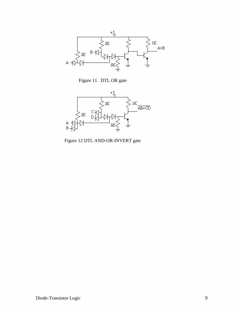
Diode-Transistor Logic 9
Figure 11. DTL OR gate
Figure 12 DTL AND-OR-INVERT gate

Transistor-Transistor Logic 1
Chapter 6 TRANSISTOR-TRANSISTOR LOGIC
The evolution from DTL to TTL can be seen by observing the placement of p-n junctions. For example, the diode D2 from Figure 2 in the chapter on DTL can be replaced by a transistor whose collector is pulled up to the power supply; transistor Q2 in Figure 1 below. The p-n junction of D2 is replaced by the BE junction of Q2 and with the current gain of the transistor, the current going into the base of Q3 is greatly increased, increasing the fanout.
Figure 1. TTL Gate. Figure 2. Configuration of Q1 as a 3-emitter transistor. The input diodes and D1 are replaced by the multi-emitter NPN transistor, Q1, in Fig. 1 and represented by the drawing in Figure 2. Later on, we will make additional modifications to this curcuit to improve its performance further. The analysis of this circuit follows very much the same path as the analysis of the DTL gate. For the most part, we will consider the input transistor, Q1, to act just like two diodes. The transistor Q2, however, will operate in all three regions. The treatment of the output voltages and currents will be treated the same as the DTL gate and Q3 will either be cutoff or saturated, corresponding to an output high and an output low, respectively. ANALYSIS WITH ONE OR MORE INPUTS LOW With an input low, Q3 should be cutoff. We will assume Q2 is cutoff and then check our assumption. If Q2 is cutoff, then there can be no current coming out of the collector of Q1, hence its base-collector junction can be modeled as an open circuit. The base-emitter junction of Q1 will be conducting. The circuit with these models substituted for the transistors is shown in Figure 3. Note the similarity to the DTL circuit under the same conditions. The two unused inputs are assumed to be high, and are thus, modeled as open. From this case, we can see that VoH = 5 volts with no load, and IinL = -I1 = -(5-0.9)/4K = -1.025 mA
dell
Text Box

Transistor-Transistor Logic 2
Figure 3. TTL circuit model with one input low. We turn now to finding VInLmax. We will use the criterion that Vin will be considered as a low as long as Q3 is kept cutoff. If the base voltage for Q3 can be raised to 0.5 Volts without turning it on, then there will be 0.5 mA current in the 1KΩ resistor. This current can only come from Q2, which means it must be conducting. Even assuming all this 0.5 mA comes through the collector of Q2, the voltage drop across the 1.4 KΩ resistor will be 0.7 Volts, not enough to cause the transistor to saturate. Thus, the active model for Q2 is appropriate as shown in Figure 4.
Figure 4. TTL circuit model to determine VinLmax. If we assume that β=30, the base current in Q2 is I mAB
mA2
0 51
0 531 0 016= = =+
. . .β Because this current is coming out of the collector of Q1, the base- collector junction of Q1 is on, and is modeled as a diode in Figure 4. The voltage at B1, the base of Q1, is VB1 = 0.5 + 0.7 + 0.7 = 1.9 Volts The current coming down through the 4 KΩ resistor, I1, is
IK
mA150 19
40 775= − =. . .
This is considerably more than is going into the base of Q2, therefore, the input BE junction of Q1 will also still be conducting. The maximum voltage at the input is VinLmax = 1.9 - 0.7 = 1.2 Volts

Transistor-Transistor Logic 3
CALCULATIONS WITH INPUT HIGH The circuit model for the TTL gate with all inputs high is shown in Figure 5. Both Q2 and Q3 are modeled as saturated, an assumption that must be verified. With the inputs high, Q1 is modeled as two diodes with the B-E diodes cutoff, and B-C diode conducting.
Figure 5. TTL gate circuit model with all inputs high. The voltage at the base of Q1 is VB1 = 0.8 + 0.8 + 0.7 = 2.3 Volts. The current down through the 4 KΩ resistor, I1 is
IK
mA150 2 3
40 675= − =. . .
All this current goes into the base of Q2. IB2 = 0.675 mA If Q2 is saturated, voltage at its collector terminal is VC2 = 0.8 + 0.2 = 1.0 Volts And the collector current is
IC2 = IK
mA250 10
142 857= − =. .
..
Clearly, if β = 30, βΙB2 > IC2 , and, therefore, Q2 is saturated. The current coming out of the emitter of Q2 is the sum of the base and collector currents. Part of this current will go down through the 1 KΩ resistor to ground and the rest will enter the base of Q3. IB3 = IB2 + IC2 - I3 = 0.675 + 2.857 - 0.8 = 2.732 mA

Transistor-Transistor Logic 4
The maximum collector current that Q3 can carry and still be in saturation is βIB3 =81.96 mA, assuming β=30. The maximum current the gate can sink when the output is low IoLmax = ICsatmax - I4 = 81.96 - 1.2 = 80.76 mA Now let's turn our attention back to the input and determine VinHmin and IinH . We will define the input voltage to be high as long as no current goes out the input terminal. Thus, all we have to do is keep the input voltage high enough so that the B-E p-n junction of Q1 does not turn on. Thus, VinHmin = 2.3 - 0.6 = 1.7 Volts CALCULATION OF IinH With the input voltage at a high, say 5 volts, the transistor Q1 will be operating in the reverse active mode. The B-E junction is reverse biased, and the B-C junction is forward biased with a base current of 0.675 mA. If there were significant curent gain, you would expect to see a large current going into the input. However, the reverse β is typically on the order of 0.02. Thus, IinH = βR ∗ I = 0.02 ∗ 0.675 = 0.0135 mA This current would add to the current going into the base of Q2, but is ignored because it is quite small and because βR is made as small as possible and this input current is a maximum and cannot be counted on. THE TOTEM POLE OUTPUT STAGE One of the problems with the TTL gate circuit we have been analyzing is that the pull-up resistor on the output transistor will prevent rapid charging of any wiring capacitance on the output. One way to improve the rise time is to reduce the resistance value as is often done, but this also increases the power dissipation when the output is low. If we look at the circuit, we observe that when the transistor is saturated, it presents a very low effective resistance to ground. The problem arises when the output is high and the pull-up resistor is too large. Ideally we would like to have a very low resistance pull-up when the output is high, but a very high pull-up resistance when the output is low. In this way, we could get quick charging and very low power dissipation. The totem-pole output stage for TTL, shown in Figure 6, does just that.
Figure 6. TTL gate with totem-pole output.

Transistor-Transistor Logic 5
This circuit operates just like the original circuit except that Q4 is on when the output is high and off when the output is low. We need to verify this operation. OUTPUT LOW Figure 7 shows the TTL circuit with all inputs high and the output low. The models for the transistors are shown as before, except diode D and transistor Q4 are added and shown as cutoff.
Figure 7. TTL gate with totem-pole output circuit model with inputs high. The analysis of this circuit proceeds exactly the same as before. The currents, I1, I2, I3, and IB3 are the same as before. With the diode and Q4 not conducting, IoLmax is now the same as IC4max , 81.96 mA. We only need to show that the diode D and transistor Q4 are indeed off. The voltage at the bottom of the diode is 0.2 Volts and the voltage at the base of Q4 equal to the voltage at the collector of Q2; VC2 = (0.2 + 0.8) = 1.0 Volts. Thus, the voltage across the B-E junction of Q4 plus the diode is 0.8 Volts. If one conducts, the other must also. To take both out of cutoff would require at least 0.5 + 0.6 = 1.1 Volts. Thus, both are off. OUTPUT HIGH This condition occurs when one or more inputs are low. The circuit is shown in Figure 8 with the appropriate models used for the transistors and the diode. In this case, Q2 and Q3 are both cutoff while Q4 and the diode are conducting. We have to assume here that there is some load and that the output current is not zero.

Transistor-Transistor Logic 6
Figure 8. TTL totem-pole circuit model with output high. The current coming out the output terminal IS (=-Io ) is the sum of the currents coming down through the base and the collector. Thus, IS = IB4 + βIB4 Because each TTL load represents 13 µA, if we assume there are 10 loads, then IS = 130 µA. The base current is
I A AB41301
4 2=+
=µβ
µ.
where we have assumed a β of 30. Then taking the path down through the 1.4 KΩ resistor to the output. the output voltage is Vo = 5.0 - 4.2µΑ∗ 1.4K - 0.7 -0.7 = 3.6 Volts The voltage drop across the 1.4 KΩ resistor is neglegible. Of course as the current increases, the output voltage will drop further. TERMINAL SPECIFICATIONS OF THE TTL GATE We are now ready to make the table showing the terminal specifications for the TTL gate. These are shown in Table 1. ------------------------------------------------------------------------------------------------ Table 1. Terminal Specifications For TTL VinLmax = 1.2 V VoL = 0.2 VinHmin = 1.7 VoH = 3.4 (@Io = -130 µA) IinL = -1.025 mA IoLmax = 81.96 mA IinH = 13 µA IoH = undetermined

Transistor-Transistor Logic 7
Figure 9. Data for ‘00, ‘04, ‘10, and ‘30 NAND gates for several TTL families (Abstracted from Texas Instruments TTL Data Book.)

Transistor-Transistor Logic 8
MANUFACTURER’S DATA SHEETS The terminal specifications of several TTL families are shown in Figure 9. You will note the values given for various voltages and currents are quite different from those we calculated. This difference comes from the fact that manufacturing tolerances and variations cannot be closely controlled, hence, the specifications given by the manufacturers are much more conservative than our calculations which were based on nominal values. Also note that the limits are usually given as a maximum or a minimum, depending on which limit is normally used in design. For example, IinLmax is given as -1.6 mA for the 74xx series. What this means is that as a designer, your driver must be able to sink as much as 1.6 mA when the input to the gate is pulled low. You will note that the TTL gate is rather loosely specified. The question invariably arises as to how one reads the data sheets or designs with this data. Figure 10 shows the allowed operating regions for a 7400, 2-input NAND gate. The best description of these operating regions is probably given by the following examples. Example 1: If the input voltage is between 0.00 and 0.08 volts, the output voltage will be
below VCC and above 2.4 volts as shown in Figure 10a. Example 2: If the input voltage is between 2.00 and VCC, the input current will be
between 0 and 40 µA as shown in Figure 10b. You will note in the above examples that there is no mathematical relationship between one variable and another. There is simply not enough data to develop one and the variability of the manufacturing process prohibits the manufacturer from providing one. In a design setting, you must stay within the limits provided by the manufacturer. For example, if you wanted to connect a resistor from the output of a 7400 gate and ground, what would be the limits allowed on the resistance value? Figure 10c provides part of the answer. If we assume that we must operate within the shaded region which represents a “High” level output, we should not allow the output to drop below 2.4 volts with 400 µA coming out of the gate. The minimum value would be 6 KΩ. The upper limit is, of course, infinite; an open circuit (Vo = VCC, Io = 0). There are a few data points provide by the specifications that are not within the limits of normal operation. For example, if the input voltage drops below zero, it is allowed to drop to -1.5 volts where you may expect as much as 12 mA coming out of a 7400 gate input. Most of this current comes from an input clamp diode which has not been shown on our drawings.

Transistor-Transistor Logic 9

Transistor-Transistor Logic 10
Another non-standard data point of interest is IoS, the short-circuit output current. This is the current you get from the gate output if the output is shorted to ground when the output of the gate would otherwise be high. In this case, both minimum and maximum values are given, -18 to -55 mA. If you went to the laboratory and actually performed this deed, you could expect a current somewhere in this range. How does this affect the designer? For example, a designer might be tempted to connect the output of the 7400 gate directly to the base of an NPN transistor whose emitter is grounded. In this case, the "high" output voltage is clamped at 0.80 V by the BE junction. What current can you expect into the base of the transistor when the gate output goes "high"? This condition is tricky and perhaps open to some debate, but the conservative designer must recognize that the operation is between the short circuit case and the case where VoHmin=2.4V when IoH =-400µA. The conservative designer would conclude that the current might be as low as 400 µA and as high as 55 mA; the worst cases. It is possible to go back to the circuit of the gate with 0.8 volts at the output terminal and calculate the current. However, this analysis would be for nominal values only and not provide definitive limits on the current. Note the notation at the bottom of the specification table in Figure 9. This notation discusses the limit on the amount of time a short circuit is allowed to be connected to the output of some gates. This time limit is based on the amount of time it takes the internal components of the integrated circuit to heat up to its maximum allowed value. While connecting a transistor base to the output is not exactly a short circuit, it is outside the allowed operating region and probably should have the same time limits as the short circuit. TERMINAL CHARACTERISTICS During the previous discussions on TTL, we were looking at circuit operation and developing an understanding of how the terminal specifications were arrived at. Let us now take a broader look at these characteristics. First, the input currents are quite high when the input is low, requiring the driver to sink a lot of current. When the input is high, the input current into the gate is quite low. Thus, any circuit which is supposed to drive the input to a TTL gate must concentrate on sinking current, and only needs to source a little current when the driver output voltage is high. Second, the output strength of the TTL gate matches the strength requirements at the input. An example is given in Figure 11. The TTL gate can sink a large current when its output is low, but can only source a small current when the output is high. Thus, if the TTL gate is expected to drive a circuit that is not another TTL circuit, you must exercise care when designing the interface. The load circuit must not require large input currents when its input is high, but may use larger currents when the input voltage is low.

Transistor-Transistor Logic 11
Figure 11. When driving other TTL gates as loads, a 7400 gate must be able to sink more current than it needs to source.
These requirements must be kept in mind when designing interfaces with the TTL gate at both the input and the output. Examples of interfacing with TTL gates are shown in Figure 12 and 13. See data books for more complete data.

Transistor-Transistor Logic 12
Figure 12. Several ways to drive loads from TTL gates.
Figure 13. Several interfaces to drive TTL gates.

Transistor-Transistor Logic 13
WIRED-AND CONNECTION Because the active pull-up or totem-pole output of the TTL gate always has one transistor cutoff and the other turned on, you cannot connect two outputs together. If one is trying to pull the output high, and the other is trying to pull it low, you will have a very low impedance path to ground and very large currents. For the same reason, the output must not be connected to any voltage source or to ground through a low impedance path. In one state or the other, there would be a low impedance path and large currents. OPEN COLLECTOR GATES In order to overcome the limitations created by the totem pole output circuit, some gates are manufactured with the output collector left open. One example is the 7405, a quad 2-input NAND gate with open collector outputs. If you connect a resistor as the pull-up, you can use this resistor to source current when the output is high and/or you can wire-AND the collectors together. TTL FAMILIES As the designers of TTL gates became more sophisticated, they developed modifications which would provide special characteristics. The original series of TTL was designated as 74XX, where the XX is replaced by logic function ( 00 is a quadruple 2-input NAND, 04 is a hex inverter, etc.) The 74LXX series is a low power family. 74HXX is a high speed family. 74SXX is a family based on Schottky diodes and transistors. 74LSXX is a family of low power Schottky. A 54xXX is also provided as a companion family to the 74xXX families. The 54... families are identical to the 74... families, except for operating temperature range and tolerance on power supply voltage. Each family has different characteristics, but the same logic functions. The L family is low power, but is much slower than the standard family. The H family is high speed, but also has higher power dissipation. The Schottky families are quite fast without increasing the power dissipation. More recent advances in TTL family have given us several other versions. For example, 74F, 74AS, and 74ALS, for Fast, Advanced Schottky, and Advanced Low-power Schottky. The AS family is the fastest, with a propagation delay of less than 5 ns. Table 2 shows the propagation delays and power supply current for each type of gate. The power supply current, ICC, is the average for a 50% duty cycle with the output spending half its time low and half the time at a high. In addition, these different families use slightly different circuit configurations. A little study of the circuits will reveal the same operations.

Transistor-Transistor Logic 14
Table 2. Propagation delays and power supply current for TTL families Data abstracted from Texas Instruments TTL Data Books
Gate tPLH (ns) tPHL (ns) ICC (mA) min typ max min typ max typical
7400 11 22 7 15 2.00 74L00 35 60 31 60 0.20 74H00 5.9 10 6.2 10 4.50
74LS00 9 20 10 20 0.40 74S00 2 3 4.5 2 3 5 3.75
74ALS00 3 11 2 8 1.00 74AS00 1 5 1 4 6.20
SCHOTTKY TTL A Schottky PN junction is made up of a semiconductor and a metal. This kind of junction has two characteristics: low turn-on voltage and low junction capacitance. When a Schottky junction is used in place of or in parallel to the Base-Collector junction of a transistor, the transistor is faster because of the lower junction capacitance and because the transistor cannot go so deep into saturation. Because the turn-on voltage for the BC junction is lower, VCEsat is higher. Schottky TTL is thus faster than standard TTL and the terminal voltages are slightly different. See the data sheet. TRI-STATE OUTPUT The totem-pole output of a TTL gate provides additional speed at lower power for the gate than a simple pull-up resistor. The cost, however, is that the gate outputs cannot be connected in parallel. This problem is serious when you need to make a bus structure such as a data bus, where several gates need to put data onto the bus at different times. The outputs can be OR'd or AND'ed using appropriate gates, but this solution is less than satisfactory and slows down the operation. A better solution is the TRI-STATE output as shown in Figure 14. The added input allows normal operation of the gate when the "enable" input is high. Both output transistors are cutoff when "enable" is low.

Resistor-Transistor Logic 1
Chapter 4 Resistor-Transistor Logic
Resistor-transistor logic, RTL, is an old technology that is no longer commercially available. It is a useful starting place to study logic gates because it is a logical extension of the transistor inverter studied in the previous chapter, and because it is a useful circuit in itself. A two-input gate is shown in Figure 1. As with most logic, the transistors operate only in saturation or cutoff. There are four possible combinations of logic inputs, L-L, L-H, H-L, and H-H for inputs A and B respectively. A low input will cutoff the associated transistor, and a high input will saturate it. Figure 2 shows these combinations where the transistors have been replaced by their corresponding models. If both transistors are cutoff, the output will be high, 3.0 Volts. If either transistor is saturated, the output will be 0.2 Volts, or low. The truth table for this gate is given in Figure 3 and shows that the gate performs a logic NOR function.
Figure 1. RTL gate Figure 3. Truth table for RTL gate
a. L-L inputs b. L-H inputs
c. H-L inputs d. H-H inputs Figure 2. RTL gate with four combinations of inputs
Dr. Ehab AL-Hialy Digital Electronics
dell
Text Box

Resistor-Transistor Logic 2
Our job is to determine the eight terminal specifications, input and output voltages and currents when these terminals are both high and low as shown in Table 1. Definitions of these terms are given in Appendix A.
Table 1. The Eight Terminal Specifications to be Determined. VinH VinL I inH IinL VoH VoL IoH IoL We begin the calculation of the terminal specification by noting that when a transistor is saturated, the collector-emitter voltage is 0.2 volts. The output terminal is connected directly to the collector terminal, thus, VoL = 0.2 volts. Assume the gate on which this analysis is taking place is embedded in a logic system. Its inputs are driven by other identical logic gates. Then if the outputs of those driver gates are logic low, the inputs to the device under analysis are low. We will use this as a starting place for the calculations. VinL = 0.2, (LOW input to both transistors) Under this condition, both transistors will be cutoff, making the output high. The circuit diagram with circuit models for the cutoff transistors is shown in Figure 4. The output voltage then is 3.0 Volts. We will call this a no-load condition when there is no load connected to the output. VoH = 3.0 Volts (No-Load)
Figure 4. RTL gate with both inputs low. The transistors are replaced by the cutoff model.
Also note from Figure 4 that the input current is zero because the transistor is cutoff. Thus, IinL = 0 The question naturally arises about how high the input voltage may rise and still keep the transistor cut off. The input voltage must stay below VBEγ to guarantee the transistor is off, making
Dr. Ehab AL-Hialy Digital Electronics

Resistor-Transistor Logic 3
VinLmax = 0.5 Volts. The maximum value is given in this case because we need to know how high it may rise. This means that the input voltage may rise as high as 0.5 volts and still keep the transistors off, and will always be recognized by the gate as a "low". INPUT HIGH In this case we want the transistor to be saturated. Either transistor saturated will cause the output to go low, to 0.2 volts. This case is shown in Figure 5. We show the circuit with one of the transistors cutoff, although both saturated would produce the same result. We start by determining the minimum input current that will keep the transistor in saturation.
Figure 5. RTL gate with one input high.
Ik
mACsat = − =30 0 20 640
4 375. ..
.
The minimum base current to keep the transistor saturated is (assuming β=30)
I I mAinHCsat
min. .= = =
β4 375
300146
The minimum value is of interest because this current is dependent on the input voltage. From this value, we can determine the minimum input voltage that will be guaranteed to be recognized as a "high". VinHmin = 0.8 + 0.146 mA x 0.450 KΩ = 0.866 Volts Any input voltage greater than or equal to 0.866 volts will cause the transistor to be saturated, and thus be recognized as a "high". We previously found VinLmax =0.5 volts. Any input voltage between 0.5 and 0.866 is an invalid logic level and the manufacturer assumes no responsibility if you provide an input voltage in that range. For the gate with no load, the relationships between input and output voltages are presented graphically in Figure 6. The noise margins NMH and NML are defined in Appendix A.
Dr. Ehab AL-Hialy Digital Electronics
dell
Text Box
B

Resistor-Transistor Logic 4
Figure 6. Graphical representation of input voltage ranges and output voltages for the unloaded RTL gate.
CALCULATIONS WHEN THE GATE IS USED TO DRIVE OTHER GATES Up to this point we have done all calculations assuming no load on the gate. While convenient for visualization, it is not a very useful situation. Let us look at the loading of the gate as if it were embedded in a logic system driving identical gates as shown in Fig. 7.
Figure 7. Driver gate being analyzed driving load gates.
Figure 8. Driver with loads when driver output is low.
Dr. Ehab AL-Hialy Digital Electronics

Resistor-Transistor Logic 5
There are two cases, the driver output being low as shown in Figure 8, and the driver output being high as shown in Figure 9. When the output is low, the driver transistor is saturated and the output is 0.2 Volts. All the input transistors of the load gates are cutoff and no current flows. The output voltage remains at 0.2 volts, unchanged by the loads.
Figure 9. RTL gate with N loads when driver output is high. However, when the output is high, the load gates require current, pulling the output voltage down. This situation is shown in Figure 9 with an unspecified number of loads. How many can you connect and still expect the gates to work right? This is called the maximum fanout. The output voltage is determined by the load current being SOURCED by the driver. VoH = 3.0 - Is x 0.64 kΩ Where the current coming out of the driver gate is divided between the load gate inputs. Since the minimum voltage at the load gate inputs when high is 0.866 Volts, this is the lowest the output voltage of the driver gate may go. Thus,
Ik
mAoHmax. .
..= − − = −30 0866
0 643334
The negative sign comes about because currents are always defined as positive when going into the terminal. Each load requires a minimum of 0.146 mA as input current, therefore, the maximum fanout is
MaxFanout ≤ =33340146
22 8..
.
Thus, the maximum fanout is 22. PRACTICAL FANOUT
Dr. Ehab AL-Hialy Digital Electronics

Resistor-Transistor Logic 6
The maximum fanout will not provide for any noise margin. Also, manufacturing tolerances will not allow such close calculations. Therefore, most manufacturers limit the allowed fanout to a much smaller number than found by nominal and typical calculations. Typically, the fanout would be limited to say 5 loads. In this case, the output voltage under maximum load would be substantially higher than calculated above. With five loads, the output current will be
I mAoH = − −
+= −30 08
0 64 0 455
3014. .
. . .
and the output voltage will be VoH = 3.0 - IoH x Rc = 3.0 - 3.014 mA x .64 kΩ = 1.071 Volts Under this condition, the Noise Margin High is NMH = 1.071 - 0.866 = 0.205 Volts Note that in many cases the output voltage will be higher than the value just calculated and thus the noise margin larger. If we define the maximum allowed fanout to be five, then VoHmin = 1.071 Volts. CALCULATION OF IoL If we define the maximum allowed fanout to be five, then the minimum voltage ever seen by the input will be 1.071 Volts. The minimum current into the input will be
Ik
mAinH min. .
..= − =1071 0 8
0 450 602
The maximum collector current is β times this or 18.067 mA and still stay in saturation. Thus, the maximum output current when the output is low is this current minus the current down through the 640 Ω resistor. IoLmax = 18.067 - 4.375 = 13.692 mA We now have all the specifications for this gate. The results are shown in Table 2. We have assumed here that the fanout is limited to 5 loads. There is a certain amount of arbitrariness in the choice of VoH and IoH. Many other performance requirements could have been chosen. The values given are self consistent, however. First note that VoHmin>VinHmin and VoLmax<VinLmax, as shown in Figure 10. The voltages are compatible.
Dr. Ehab AL-Hialy Digital Electronics

Resistor-Transistor Logic 7
Figure 10. Voltage compatibility chart, with 5 loads To determine fanout,
IIoH
inH
= 5 007. and IIoL
inL
= ∞
Therefore, the fanout is 5. ---------------------------------------------------------------------------- Table 2. Terminal specifications for the RTL Gate VinLmax = 0.500 Volts VoL = 0.2 Volts VinHmin = 0.866 Volts VoHmin = 1.071 Volts (N=5) IinL = 0 IoLmax = 13.692 mA (Vin > VoHmin) IinHmin = 0.602 mA IoHmax = - 3.014 mA ---------------------------------------------------------------------------- INTERFACING TO RTL Table 2 is a set of specifications that would be provided by the manufacturer of the RTL logic. From this information, you would be expected to be able to use the gates without exceeding any specification. Any gate embedded in a logic system using only the RTL gates analyzed, would be guaranteed to work within the specifications. The only limitation we must follow is limiting the fanout to five loads. However, logic is rarely used without interfacing to the outside world at some point. There must be some signals at some point that are generated outside the logic system that must be recognized as a logic one or a zero. Similarly, there is usually some point where a logic gate output must drive a device that is not another gate.
a. b. c. Figure 11. Three possible configurations of a switch-to-logic gate interface.
Dr. Ehab AL-Hialy Digital Electronics

Resistor-Transistor Logic 8
Figure 11 shows three possible connection using a switch to generate the logic inputs to a gate. In Figure 11a the switch is used as a pull-down to make the input voltage a logic zero when the switch is closed. The resistor pulls the input voltage up to a logic one when the switch is open. Looking at the specifications in Table 2, we note that when the switch is closed, the input voltage is zero volts, well below the required VinLmax of 0.5 volts. The gate input current is zero so the switch needs only to handle the current coming down through the resistor. When the switch is open, current will come down through the resistor into the gate input terminal. The specifications show the voltage must be above 0.866 volts and the current must be at least 0.602 mA. From these values, we can select a value of R1. To provide a noise margin, we should certainly provide a voltage at least as high as VoHmin = 1.071 volts. Let's shoot for 2.0 volts to provide even greater noise margin. We know this will provide greater than the minimum current, but we don't yet know how much. We now have to put on our engineer's hat and look inside the gate to finish the design. The parts of the circuit that pertain to this case are shown in Figure 12 with only the base-emitter voltage of the transistor shown. The transistor must be in saturation so we use 0.8 volts for VBEsat.
Figure 12. Circuit with switch open. Solving this circuit, we can write a single node equation at the input node, Vin = 2.0 v, (3.0-2.0)/R1 = (2.0-0.8)/450 Solving, we get R1 = 375 Ω. This is not a standard resistor value so we would select a nearby standard value and re-solve the circuit, this time to determine the input voltage. If we are satisfied with the result, then we are finished. If the input voltage found is not satisfactory, we would try with another value. Note that we do not have to get 2.0 volts, we simply chose that value as a place to start the design. We do, however, have to provide Vin > VinHmin. The design of the circuit in Figure 11b would follow a similar track. Notice that in this circuit the input voltage is high when the switch is closed; the opposite of the circuit in Figure 11a. Figure 11c is simpler than 11b, but it is not recommended because when the switch is open, the input lead of the gate is floating or disconnected and susceptible to noise which might cause random errors in the logic.
Dr. Ehab AL-Hialy Digital Electronics

Resistor-Transistor Logic 9
Figure 13 shows an example of an interface at the output of the gate. In this case, we want to drive an LED at 30 mA. Neither the high nor low output currents of the gate are sufficient, so we use a transistor as a current amplifier. Many other configurations are possible and some may be preferrable depending on the application. We will not go through the design of this circuit here. A similar circuit was designed at the end of the previous chapter.
Figure 13. Example of an output interface circuit.
Dr. Ehab AL-Hialy Digital Electronics

Emitter-Coupled Logic 1
Chapter 7 EMITTER-COUPLED LOGIC
The major speed limitation of TTL is the turn-off time of saturated transistors. To be sure, TTL has come a long way from the 100 ns time of DTL to the 2-4 ns propagation delays of ASTTL. ECL is designed so that the transistors are either cutoff or in the active region, rather than cutoff or saturation for the DTL/TTL. With the transistors in the active region, the charge stored in the base region of the transistors is kept to a minimum, allowing shorter turn-off times. Typical propagation delays of "standard" ECL are about 1 ns, and down to about 0.5 ns for some of the advanced types. There are several disadvantages associated with ECL. It uses a negative power supply so that the logic levels are not compatible with any other logic family, and makes analysis and measurement inconvenient. ECL requires large currents and the noise margins are small. On the other hand, power supply currents remain much more stable when the logic switches compared to TTL, thus reducing noise on the power leads. In practice, ECL is used only when necessary for its high speed. ECL has been around since the early 60's, being developed at about the same time as DTL. Before we start the analysis of the circuit, we need to look at the circuit model we will use for the transistors in the ECL circuit. Because ECL is predicated on speed, the size of the transistors is as small as possible to keep stored charge to a minimum. Thus, current densities and hence, voltage drops will be slightly higher than normal. For this reason, we will use different voltages for base-emitter voltage for ECL. VBEγ = 0.65 and VBEactive = 0.75 volts ECL is based on the emitter coupled pair shown in Figure 1. This pair will have one transistor on and the other cutoff in each logic state. If we compare the currents through the two transistors, one with 0.75 volts between base and emitter and the other with 0.65 volts, we will find that the transistor with the higher voltage will be carrying nearly 50 times the current of the other. Thus, the lower voltage transistor will essentially be cutoff.
II
I e
I e
B
B
oV
oV
T
T
1
2
0 75
0 65 47 5= =
.
. . where VT = 25.9 mV
dell
Text Box
Dr. Ehab
Highlight
Dr. Ehab
Highlight
Dr. Ehab
Highlight

Emitter-Coupled Logic 2
Figure 1. Emitter coupled Pair BASIC OPERATION OF THE EMITTER-COUPLED PAIR We start by looking at the operation of the difference amplifier shown in Figure 1. The two transistors are connected at their emitters. The base of Q2 is connected to a reference voltage, VR. Consider for an example, that the input voltage is low enough to keep Q1 cutoff. Then, Q2 will be conducting and the emitter voltage will be VE = VR - VBEon = VR - 0.75 assuming Q2 is operating in the active region. We know Q2 is in the active region because the collector resistors are selected to keep the transistors from saturating. How high can we raise the input voltage and still keep Q1 off? VinLmax = VE + VBEγ = VR - 0.75 + 0.65 = VR -0.10 volts Now, let the input voltage start rising above this voltage. Then Q1 begins to turn on. This increases the current through RE, raising the voltage at the emitters. This voltage rise causes Q2 to begin to turn off. The input voltage rises only a little bit before Q2 turns off entirely. The minimum high level input voltage occurs when VE = VR -0.65 and VinHmin = VE + 0.75 = VR + 0.10 volts Thus, a 200 mV swing at the input causes a complete reversal in which transistor is turned on and which is turned off. ANALYSIS OF THE ECL GATE We now turn our attention to Figure 2, the complete ECL gate circuit. In this circuit we have added two emitter follower output stages. As we shall see later, these output stages serve the purposes of buffering the gate output, providing added fanout, as well as shifting the voltage levels.

Emitter-Coupled Logic 3
Figure 2. Complete ECL Gate OR OUTPUT --- Output high, Q2 off With Q2 off, the output circuit looks like that shown in Figure 3.
Figure 3. Equivalent Circuit With Q2 OFF. If we assume a very high β, we can ignore base current (I2 ≅ 0) but the transistor Q6 is in the active region so VoH = Vo2 ≅ -0.75 volts (Note that since the collector is at 0V, and the emitter is at -0.75V, the transistor is in the active region. This type of circuit is called an emitter follower. The output voltage is always VBEactive below the base voltage and follows the base voltage, even when the output goes low as we shall see next.)
Figure 4. Equivalent Circuit With Q2 ON.
Dr. Ehab
Highlight

Emitter-Coupled Logic 4
OR OUTPUT LOW - Q2 ON, Q1 OFF, The circuit for this case is shown in Figure 4. The emitter voltage is: VE = VR - 0.75 = -2.07 volts Thus, the current down through the emitter resistor is
I mAE = − − − = =2 07 5 2779
313779
4 018. ( . ) . .
If we assume β is very large so base currents can be neglected, the collector current in Q2 will be the same as the emitter current. Thus, the voltage at the collector of Q2 (and the base of Q6 ) will be VC2 = VB6 = -IC2∗ 245 = -0.98 (Note that VC2 - VE = 1.09v. Q2 is in active region.) Thus, the voltage at the emitter of Q6 will be VoL = Vo2 = -0.98 - 0.75 = -1.73 volts We can now plot the output at Vo2 versus the input voltage. The result is shown in Figure 5. NOR OUTPUT, Q1 OFF, Output High This case is essentially the same as for the OR output when it is high, except that we have a 220 Ω resistor instead of a 245 Ω resistor at the collector. Again, because the base current is so small, the output voltage will be -0.75 volts, the same as for the OR output. NOR OUTPUT, Q1 ON, Q2 OFF, Output Low. This case is similar to the OR output high case, except that the input voltage can directly affect the collector current through Q1 causing the voltage at the base of Q1 to change. As Vin increases, the current increases causing the voltage at the base of Q5 to decrease. Because the output follows the base voltage with a 0.75 volt difference, the output drops as Vin increases. This scenario holds until Q1 saturates. Then as Vin increases further, the base-collector junction is forward biased, and current flows from the input toward the collector, raising the voltage at the base of Q5, hence raising the output voltage. The resulting plot of Vo1 vs Vin is also shown in Figure 5.
Dr. Ehab
Highlight
Dr. Ehab
Highlight

Emitter-Coupled Logic 5