
Phllosophy, of Doctor of the of nents Mathematical University

Documentation
KL4112
Dual Channel Analog Output Terminal, 0 to 20 mA, 16 Bit
3.12017-12-12
Version:Date:


table of contents
KL4112 3Version: 3.1
table of contents1 Foreword .................................................................................................................................................... 5
1.1 Notes on the documentation........................................................................................................... 51.2 Safety instructions .......................................................................................................................... 61.3 Documentation issue status............................................................................................................ 7
2 Product overview....................................................................................................................................... 82.1 KL4112 - Introduction ..................................................................................................................... 82.2 KL4112 - Technical data................................................................................................................. 92.3 Basic function principles ............................................................................................................... 10
3 Mounting and wiring ............................................................................................................................... 113.1 Instructions for ESD protection ..................................................................................................... 113.2 Installation on mounting rails ........................................................................................................ 113.3 Installation instructions for enhanced mechanical load capacity .................................................. 153.4 Connection.................................................................................................................................... 15
3.4.1 Connection system........................................................................................................... 153.4.2 Wiring............................................................................................................................... 173.4.3 Shielding .......................................................................................................................... 18
3.5 KL4112 - connection and LED description ................................................................................... 193.6 ATEX - Special conditions (standard temperature range) ............................................................ 203.7 ATEX Documentation ................................................................................................................... 21
4 Configuration Software KS2000............................................................................................................. 224.1 KS2000 - Introduction ................................................................................................................... 22
5 Access from the user program .............................................................................................................. 245.1 KL4112 - Terminal configuration................................................................................................... 245.2 Mapping in the Bus Coupler ......................................................................................................... 26
5.2.1 KL4112............................................................................................................................. 275.3 Register overview ......................................................................................................................... 275.4 Register description ...................................................................................................................... 285.5 Control and status byte................................................................................................................. 30
5.5.1 Process data exchange ................................................................................................... 315.5.2 Register communication................................................................................................... 32
5.6 Examples of Register Communication.......................................................................................... 335.6.1 Example 1: reading the firmware version from Register 9 ............................................... 335.6.2 Example 2: Writing to an user register ............................................................................. 34
6 Appendix .................................................................................................................................................. 376.1 Support and Service ..................................................................................................................... 37

table of contents
KL41124 Version: 3.1

Foreword
KL4112 5Version: 3.1
1 Foreword
1.1 Notes on the documentation
Intended audience
This description is only intended for the use of trained specialists in control and automation engineering whoare familiar with the applicable national standards.It is essential that the documentation and the following notes and explanations are followed when installingand commissioning these components.It is the duty of the technical personnel to use the documentation published at the respective time of eachinstallation and commissioning.
The responsible staff must ensure that the application or use of the products described satisfy all therequirements for safety, including all the relevant laws, regulations, guidelines and standards.
Disclaimer
The documentation has been prepared with care. The products described are, however, constantly underdevelopment.
We reserve the right to revise and change the documentation at any time and without prior announcement.
No claims for the modification of products that have already been supplied may be made on the basis of thedata, diagrams and descriptions in this documentation.
Trademarks
Beckhoff®, TwinCAT®, EtherCAT®, Safety over EtherCAT®, TwinSAFE®, XFC® and XTS® are registeredtrademarks of and licensed by Beckhoff Automation GmbH.Other designations used in this publication may be trademarks whose use by third parties for their ownpurposes could violate the rights of the owners.
Patent Pending
The EtherCAT Technology is covered, including but not limited to the following patent applications andpatents: EP1590927, EP1789857, DE102004044764, DE102007017835 with corresponding applications orregistrations in various other countries.
The TwinCAT Technology is covered, including but not limited to the following patent applications andpatents: EP0851348, US6167425 with corresponding applications or registrations in various other countries.
EtherCAT® is registered trademark and patented technology, licensed by Beckhoff Automation GmbH,Germany
Copyright
© Beckhoff Automation GmbH & Co. KG, Germany.The reproduction, distribution and utilization of this document as well as the communication of its contents toothers without express authorization are prohibited.Offenders will be held liable for the payment of damages. All rights reserved in the event of the grant of apatent, utility model or design.
Foreword
KL41126 Version: 3.1
1.2 Safety instructions
Safety regulations
Please note the following safety instructions and explanations!Product-specific safety instructions can be found on following pages or in the areas mounting, wiring,commissioning etc.
Exclusion of liability
All the components are supplied in particular hardware and software configurations appropriate for theapplication. Modifications to hardware or software configurations other than those described in thedocumentation are not permitted, and nullify the liability of Beckhoff Automation GmbH & Co. KG.
Personnel qualification
This description is only intended for trained specialists in control, automation and drive engineering who arefamiliar with the applicable national standards.
Description of symbols
In this documentation the following symbols are used with an accompanying safety instruction or note. Thesafety instructions must be read carefully and followed without fail!
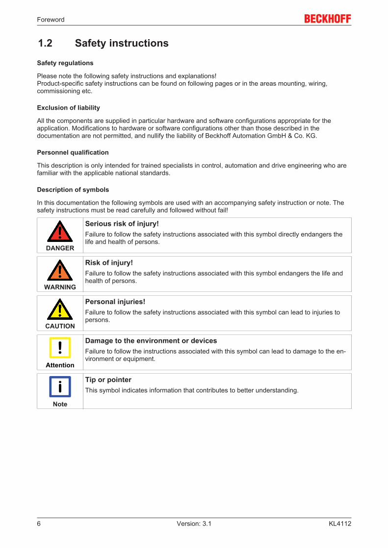
DANGER
Serious risk of injury!Failure to follow the safety instructions associated with this symbol directly endangers thelife and health of persons.
WARNING
Risk of injury!Failure to follow the safety instructions associated with this symbol endangers the life andhealth of persons.
CAUTION
Personal injuries!Failure to follow the safety instructions associated with this symbol can lead to injuries topersons.
Attention
Damage to the environment or devicesFailure to follow the instructions associated with this symbol can lead to damage to the en-vironment or equipment.
Note
Tip or pointerThis symbol indicates information that contributes to better understanding.

Foreword
KL4112 7Version: 3.1
1.3 Documentation issue statusVersion Comment3.1 • Update Technical data
• Structure update3.0 • Migration
• Update Technical data• Structure update• Chapters KS2000 configuration software and Access from the user program added
Firmware (FW) and hardware (HW) versionsDocumentation, version
KL4112FW HW
3.1 3D 033.0 3D 03
The firmware and hardware versions (delivery state) can be found in the serial number printed on the side ofthe terminal.
Syntax of the serial number
Structure of the serial number: WW YY FF HH
WW - week of production (calendar week)YY - year of productionFF - firmware versionHH - hardware version
Example with ser. no.: 35 04 1B 01:
35 - week of production 354 - year of production 20041B - firmware version 1B1 - hardware version 1
Product overview
KL41128 Version: 3.1
2 Product overview
2.1 KL4112 - Introduction
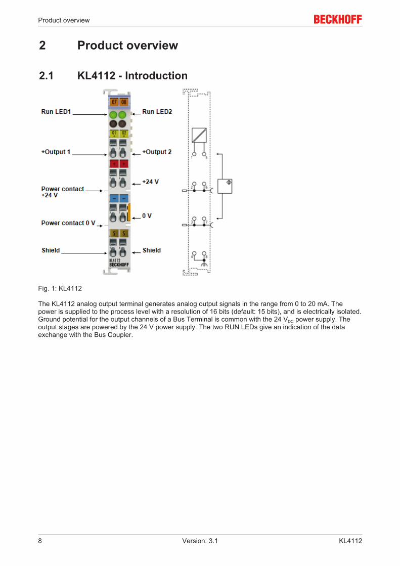
Fig. 1: KL4112
The KL4112 analog output terminal generates analog output signals in the range from 0 to 20 mA. Thepower is supplied to the process level with a resolution of 16 bits (default: 15 bits), and is electrically isolated.Ground potential for the output channels of a Bus Terminal is common with the 24 VDC power supply. Theoutput stages are powered by the 24 V power supply. The two RUN LEDs give an indication of the dataexchange with the Bus Coupler.
Product overview
KL4112 9Version: 3.1
2.2 KL4112 - Technical dataTechnical Data KL4112Number of outputs 2Power supply for the electronics 24 VDC via the power contactsSignal current 0 mA to 20 mALoad < 500 ΩAccuracy < ±0.1 % (of the full scale value), at 23 °CResolution 15 bits, configurable to 16 bitsElectrical isolation 500 V (K-Bus / signal voltage)Conversion time ~ 3.5 msCurrent consumption from the K-bus typically 60 mABit width in the K-bus I/O Output: 2 x 16 bits of data (2 x 8 bits control/status optional)Configuration No address or configuration settingsWeight approx. 80 gDimensions (W x H x D) approx. 15 mm x 100 mm x 70 mm (width aligned: 12 mm)
Mounting [} 11] on 35 mm mounting rail conforms to EN 60715
Permissible ambient temperature rangeduring operation
0 °C to + 55 °C
Permissible ambient temperature rangeduring storage
-25 °C to +85 °C
Permissible relative air humidity 95 %, no condensationVibration / shock resistance conforms to EN 60068-2-6 / EN 60068-2-27, see also Installation instructions for terminal with
enhanced mechanical load capacity [} 15]EMC immunity / emission conforms to EN 61000-6-2 / EN 61000-6-4Protection class IP20Installation position variableApproval CE, cULus, ATEX [} 20]
Product overview
KL411210 Version: 3.1
2.3 Basic function principlesThe KL4112 analog output terminal generates signals in the range from 0 to 20 mA. The terminal suppliesthe output voltage with a resolution of up to 16 bits. The output voltage is output electrically isolated from theterminal bus level.
The LEDs indicate the operating state of the associated terminal channels.
• green Run LED:◦ On: Normal operation◦ Off: Watchdog timer overflow has occurred. If no process data are transmitted by the Bus
Coupler for 100 ms, the green LEDs go out. The output assumes a user-specified voltage (seeFeature register [} 30]).
Process data input format
In the delivery state the process data are shown in two's complement form (integer -1 corresponds to0xFFFF).
Output value Process datadec hex
0 mA 0 0x000010 mA 16383 0x3FFF20 mA 32767 0x7FFF
Process data
The process data arriving from the Bus Coupler are output to the process:
Y_0 = B_a + A_a*XY_dac = Y_0
(1.0) Neither user nor manufacturer scaling is active.
Y_1 = B_h + A_h * XY_dac = Y_1
(1.1) Manufacturer scaling active
Y_2 = B_w + A_w * XY_dac = Y_2
(1.2) User scaling active
Y_1 = B_h + A_h * XY_dac = B_w + A_w * Y_1
(1.3)(1.4)
Manufacturer and user scaling active
KeyName Name RegisterX PLC process data -B_a Hardware compensation offset R17 [} 29]A_a Hardware compensation gain R18 [} 29]B_h Manufacturer scaling: Offset R19 [} 29]A_h Manufacturer scaling: Gain R20 [} 29]B_w User scaling: Offset R33 [} 30]A_w User scaling: Gain R34 [} 30]Y_dac Output value for the D/A converter -
The equations of the straight line are enabled via register R32 [} 30]

Mounting and wiring
KL4112 11Version: 3.1
3 Mounting and wiring
3.1 Instructions for ESD protection
Attention
Destruction of the devices by electrostatic discharge possible!The devices contain components at risk from electrostatic discharge caused by improperhandling.ü Please ensure you are electrostatically discharged and avoid touching the contacts of
the device directly.a) Avoid contact with highly insulating materials (synthetic fibers, plastic film etc.).b) Surroundings (working place, packaging and personnel) should by grounded probably,
when handling with the devices.
c) Each assembly must be terminated at the right hand end with an EL9011 bus end cap,to ensure the protection class and ESD protection.
Fig. 2: Spring contacts of the Beckhoff I/O components
3.2 Installation on mounting rails
WARNING
Risk of electric shock and damage of device!Bring the bus terminal system into a safe, powered down state before starting installation,disassembly or wiring of the Bus Terminals!
Mounting and wiring
KL411212 Version: 3.1
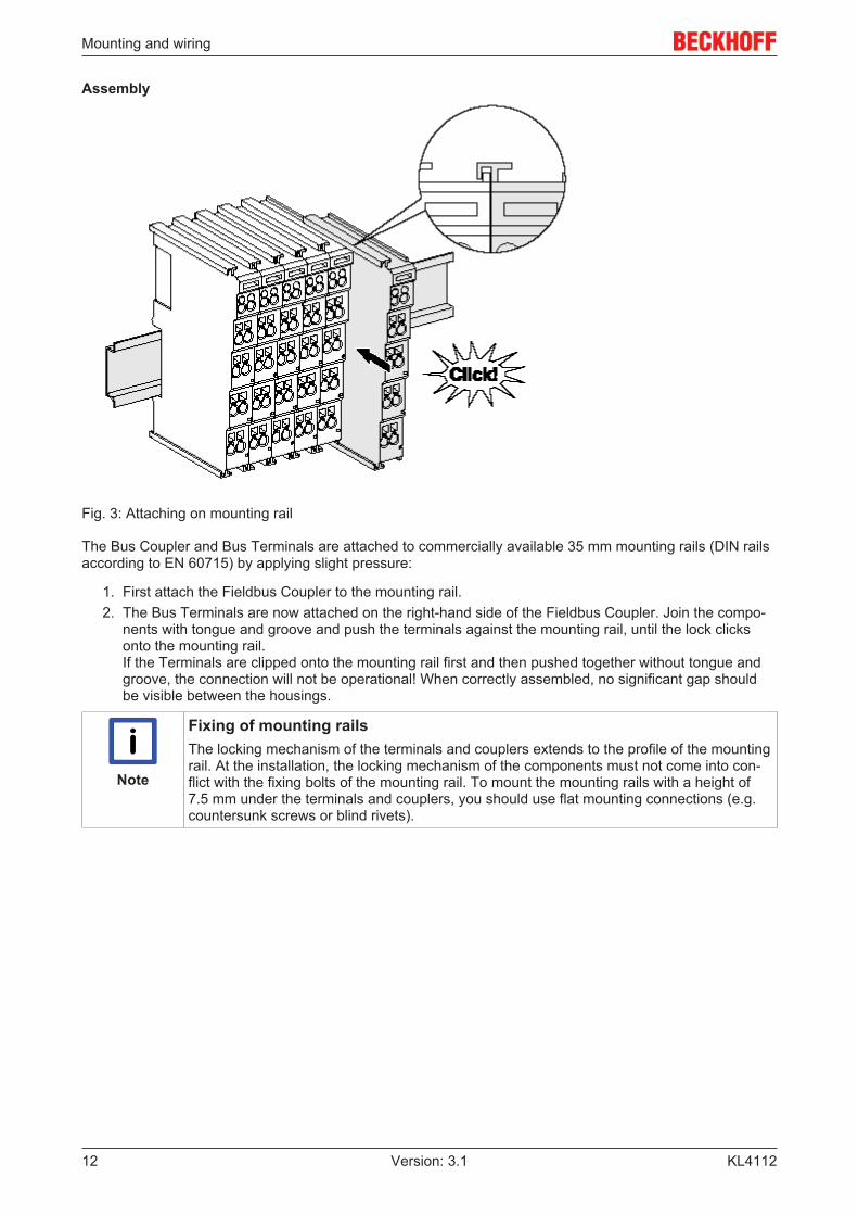
Assembly
Fig. 3: Attaching on mounting rail
The Bus Coupler and Bus Terminals are attached to commercially available 35 mm mounting rails (DIN railsaccording to EN 60715) by applying slight pressure:
1. First attach the Fieldbus Coupler to the mounting rail.2. The Bus Terminals are now attached on the right-hand side of the Fieldbus Coupler. Join the compo-
nents with tongue and groove and push the terminals against the mounting rail, until the lock clicksonto the mounting rail.If the Terminals are clipped onto the mounting rail first and then pushed together without tongue andgroove, the connection will not be operational! When correctly assembled, no significant gap shouldbe visible between the housings.
Note
Fixing of mounting railsThe locking mechanism of the terminals and couplers extends to the profile of the mountingrail. At the installation, the locking mechanism of the components must not come into con-flict with the fixing bolts of the mounting rail. To mount the mounting rails with a height of7.5 mm under the terminals and couplers, you should use flat mounting connections (e.g.countersunk screws or blind rivets).

Mounting and wiring
KL4112 13Version: 3.1
Disassembly
Fig. 4: Disassembling of terminal
Each terminal is secured by a lock on the mounting rail, which must be released for disassembly:
1. Pull the terminal by its orange-colored lugs approximately 1 cm away from the mounting rail. In doingso for this terminal the mounting rail lock is released automatically and you can pull the terminal out ofthe bus terminal block easily without excessive force.
2. Grasp the released terminal with thumb and index finger simultaneous at the upper and lower groovedhousing surfaces and pull the terminal out of the bus terminal block.
Connections within a bus terminal block
The electric connections between the Bus Coupler and the Bus Terminals are automatically realized byjoining the components:
• The six spring contacts of the K-Bus/E-Bus deal with the transfer of the data and the supply of the BusTerminal electronics.
• The power contacts deal with the supply for the field electronics and thus represent a supply rail withinthe bus terminal block. The power contacts are supplied via terminals on the Bus Coupler (up to 24 V)or for higher voltages via power feed terminals.
Note
Power ContactsDuring the design of a bus terminal block, the pin assignment of the individual Bus Termi-nals must be taken account of, since some types (e.g. analog Bus Terminals or digital 4-channel Bus Terminals) do not or not fully loop through the power contacts. Power FeedTerminals (KL91xx, KL92xx or EL91xx, EL92xx) interrupt the power contacts and thus rep-resent the start of a new supply rail.
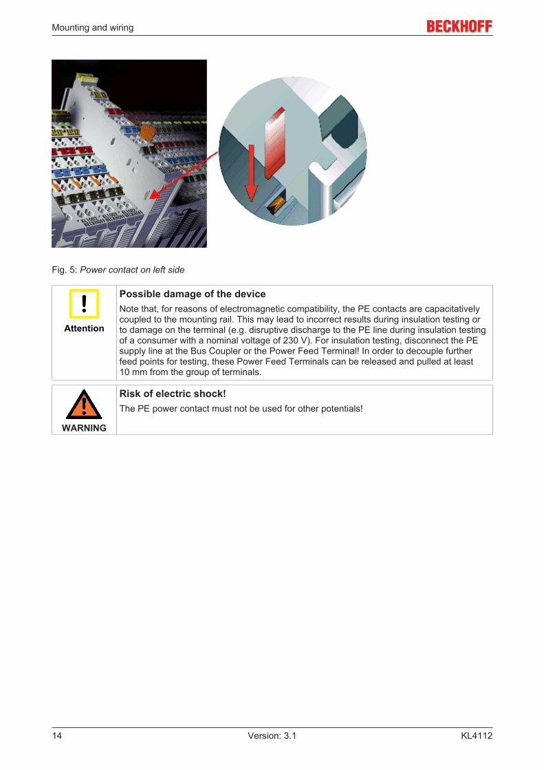
PE power contact
The power contact labeled PE can be used as a protective earth. For safety reasons this contact mates firstwhen plugging together, and can ground short-circuit currents of up to 125 A.
Mounting and wiring
KL411214 Version: 3.1
Fig. 5: Power contact on left side
Attention
Possible damage of the deviceNote that, for reasons of electromagnetic compatibility, the PE contacts are capacitativelycoupled to the mounting rail. This may lead to incorrect results during insulation testing orto damage on the terminal (e.g. disruptive discharge to the PE line during insulation testingof a consumer with a nominal voltage of 230 V). For insulation testing, disconnect the PEsupply line at the Bus Coupler or the Power Feed Terminal! In order to decouple furtherfeed points for testing, these Power Feed Terminals can be released and pulled at least10 mm from the group of terminals.
WARNING
Risk of electric shock!The PE power contact must not be used for other potentials!

Mounting and wiring
KL4112 15Version: 3.1
3.3 Installation instructions for enhanced mechanical loadcapacity
WARNING
Risk of injury through electric shock and damage to the device!Bring the Bus Terminal system into a safe, de-energized state before starting mounting,disassembly or wiring of the Bus Terminals!
Additional checks
The terminals have undergone the following additional tests:
Verification ExplanationVibration 10 frequency runs in 3 axes
6 Hz < f < 60 Hz displacement 0.35 mm, constant amplitude60.1 Hz < f < 500 Hz acceleration 5 g, constant amplitude
Shocks 1000 shocks in each direction, in 3 axes25 g, 6 ms
Additional installation instructions
For terminals with enhanced mechanical load capacity, the following additional installation instructions apply:
• The enhanced mechanical load capacity is valid for all permissible installation positions• Use a mounting rail according to EN 60715 TH35-15• Fix the terminal segment on both sides of the mounting rail with a mechanical fixture, e.g. an earth
terminal or reinforced end clamp• The maximum total extension of the terminal segment (without coupler) is:
64 terminals (12 mm mounting with) or 32 terminals (24 mm mounting with)• Avoid deformation, twisting, crushing and bending of the mounting rail during edging and installation of
the rail• The mounting points of the mounting rail must be set at 5 cm intervals• Use countersunk head screws to fasten the mounting rail• The free length between the strain relief and the wire connection should be kept as short as possible. A
distance of approx. 10 cm should be maintained to the cable duct.
3.4 Connection
3.4.1 Connection system
WARNING
Risk of electric shock and damage of device!Bring the bus terminal system into a safe, powered down state before starting installation,disassembly or wiring of the Bus Terminals!
Overview
The Bus Terminal system offers different connection options for optimum adaptation to the respectiveapplication:
• The terminals of ELxxxx and KLxxxx series with standard wiring include electronics and connectionlevel in a single enclosure.
• The terminals of ESxxxx and KSxxxx series feature a pluggable connection level and enable steadywiring while replacing.
Mounting and wiring
KL411216 Version: 3.1
• The High Density Terminals (HD Terminals) include electronics and connection level in a singleenclosure and have advanced packaging density.
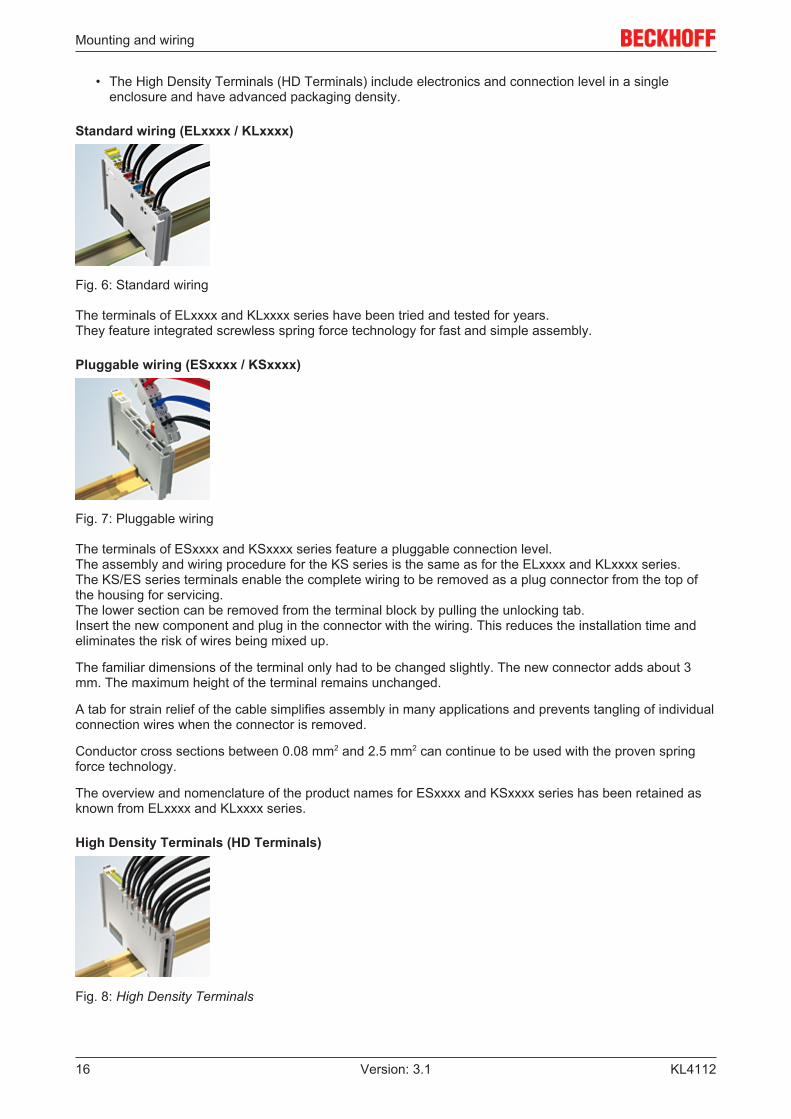
Standard wiring (ELxxxx / KLxxxx)
Fig. 6: Standard wiring
The terminals of ELxxxx and KLxxxx series have been tried and tested for years.They feature integrated screwless spring force technology for fast and simple assembly.
Pluggable wiring (ESxxxx / KSxxxx)
Fig. 7: Pluggable wiring
The terminals of ESxxxx and KSxxxx series feature a pluggable connection level.The assembly and wiring procedure for the KS series is the same as for the ELxxxx and KLxxxx series.The KS/ES series terminals enable the complete wiring to be removed as a plug connector from the top ofthe housing for servicing.The lower section can be removed from the terminal block by pulling the unlocking tab. Insert the new component and plug in the connector with the wiring. This reduces the installation time andeliminates the risk of wires being mixed up.
The familiar dimensions of the terminal only had to be changed slightly. The new connector adds about 3mm. The maximum height of the terminal remains unchanged.
A tab for strain relief of the cable simplifies assembly in many applications and prevents tangling of individualconnection wires when the connector is removed.
Conductor cross sections between 0.08 mm2 and 2.5 mm2 can continue to be used with the proven springforce technology.
The overview and nomenclature of the product names for ESxxxx and KSxxxx series has been retained asknown from ELxxxx and KLxxxx series.
High Density Terminals (HD Terminals)
Fig. 8: High Density Terminals

Mounting and wiring
KL4112 17Version: 3.1
The Bus Terminals from these series with 16 terminal points are distinguished by a particularly compactdesign, as the packaging density is twice as large as that of the standard 12 mm Bus Terminals. Massiveconductors and conductors with a wire end sleeve can be inserted directly into the spring loaded terminalpoint without tools.
Note
Wiring HD TerminalsThe High Density (HD) Terminals of the ELx8xx and KLx8xx series doesn't support plug-gable wiring.
Ultrasonically "bonded" (ultrasonically welded) conductors
Note
Ultrasonically “bonded" conductorsIt is also possible to connect the Standard and High Density Terminals with ultrasonically"bonded" (ultrasonically welded) conductors. In this case, please note the tables concern-ing the wire-size width below!
3.4.2 Wiring
WARNING
Risk of electric shock and damage of device!Bring the bus terminal system into a safe, powered down state before starting installation,disassembly or wiring of the Bus Terminals!
Terminals for standard wiring ELxxxx/KLxxxx and for pluggable wiring ESxxxx/KSxxxx
Fig. 9: Connecting a cable on a terminal point
Up to eight terminal points enable the connection of solid or finely stranded cables to the Bus Terminal. Theterminal points are implemented in spring force technology. Connect the cables as follows:
1. Open a terminal point by pushing a screwdriver straight against the stop into the square openingabove the terminal point. Do not turn the screwdriver or move it alternately (don't toggle).
2. The wire can now be inserted into the round terminal opening without any force.3. The terminal point closes automatically when the pressure is released, holding the wire securely and
permanently.

Mounting and wiring
KL411218 Version: 3.1
See the following table for the suitable wire size width.
Terminal housing ELxxxx, KLxxxx ESxxxx, KSxxxxWire size width (single core wires) 0.08 ... 2.5 mm2 0.08 ... 2.5 mm2
Wire size width (fine-wire conductors) 0.08 ... 2.5 mm2 0,08 ... 2.5 mm2
Wire size width (conductors with a wire end sleeve) 0.14 ... 1.5 mm2 0.14 ... 1.5 mm2
Wire stripping length 8 ... 9 mm 9 ... 10 mm
High Density Terminals (HD Terminals [} 16]) with 16 terminal points
The conductors of the HD Terminals are connected without tools for single-wire conductors using the directplug-in technique, i.e. after stripping the wire is simply plugged into the terminal point. The cables arereleased, as usual, using the contact release with the aid of a screwdriver. See the following table for thesuitable wire size width.
Terminal housing High Density HousingWire size width (single core wires) 0.08 ... 1.5 mm2
Wire size width (fine-wire conductors) 0.25 ... 1.5 mm2
Wire size width (conductors with a wire end sleeve) 0.14 ... 0.75 mm2
Wire size width (ultrasonically “bonded" conductors) only 1.5 mm2
Wire stripping length 8 ... 9 mm
3.4.3 Shielding
Note
ShieldingEncoder, analog sensors and actors should always be connected with shielded, twistedpaired wires.

Mounting and wiring
KL4112 19Version: 3.1
3.5 KL4112 - connection and LED description
WARNING
Risk of injury through electric shock and damage to the device!Bring the Bus Terminals system into a safe, de-energized state before starting mounting,disassembly or wiring of the Bus Terminals!
Fig. 10: KL4112 - connection and LEDs
Connection KL4112Terminal point No. CommentOutput1 1 + Output 1+24 V 2 +24 V (internally connected to terminal point 6 and positive power contact)GND 3 0 V (internally connected to terminal point 7 and negative power contact)Shield 4 PE contact (internally connected to terminal point 8)Output2 5 + Output 2+24 V 6 +24 V (internally connected to terminal point 2 and positive power contact)GND 7 0 V (internally connected to terminal point 3 and negative power contact)Shield 8 PE contact (internally connected to terminal point 4)
LED description KL4112LED Color DescriptionRun1 LEDRun2 LED
green On: Normal operationOff: Watchdog timer overflow has occurred. If no process data is transmitted to the bus cou-
pler for 100 ms, the green LEDs go out. The output assumes a user-specified voltage(see Feature register [} 30]).

Mounting and wiring
KL411220 Version: 3.1
3.6 ATEX - Special conditions (standard temperaturerange)
WARNING
Observe the special conditions for the intended use of Beckhoff fieldbuscomponents with standard temperature range in potentially explosive areas(directive 94/9/EU)!
• The certified components are to be installed in a suitable housing that guarantees aprotection class of at least IP54 in accordance with EN 60529! The environmental con-ditions during use are thereby to be taken into account!
• If the temperatures during rated operation are higher than 70°C at the feed-in points ofcables, lines or pipes, or higher than 80°C at the wire branching points, then cablesmust be selected whose temperature data correspond to the actual measured tempera-ture values!
• Observe the permissible ambient temperature range of 0 to 55°C for the use of Beck-hoff fieldbus components standard temperature range in potentially explosive areas!
• Measures must be taken to protect against the rated operating voltage being exceededby more than 40% due to short-term interference voltages!
• The individual terminals may only be unplugged or removed from the Bus Terminal sys-tem if the supply voltage has been switched off or if a non-explosive atmosphere is en-sured!
• The connections of the certified components may only be connected or disconnected ifthe supply voltage has been switched off or if a non-explosive atmosphere is ensured!
• The fuses of the KL92xx/EL92xx power feed terminals may only be exchanged if thesupply voltage has been switched off or if a non-explosive atmosphere is ensured!
• Address selectors and ID switches may only be adjusted if the supply voltage has beenswitched off or if a non-explosive atmosphere is ensured!
Standards
The fundamental health and safety requirements are fulfilled by compliance with the following standards:
• EN 60079-0:2012+A11:2013• EN 60079-15:2010
Marking
The Beckhoff fieldbus components with standard temperature range certified for potentially explosive areasbear one of the following markings:
II 3G KEMA 10ATEX0075 X Ex nA IIC T4 Gc Ta: 0 … 55°C
or
II 3G KEMA 10ATEX0075 X Ex nC IIC T4 Gc Ta: 0 … 55°C

Mounting and wiring
KL4112 21Version: 3.1
3.7 ATEX Documentation
Note
Notes about operation of the Beckhoff terminal systems in potentially explo-sive areas (ATEX)Pay also attention to the continuative documentation
Notes about operation of the Beckhoff terminal systems in potentially explosive areas(ATEX)
that is available in the download area of the Beckhoff homepage http:\\www.beckhoff.com!

Configuration Software KS2000
KL411222 Version: 3.1
4 Configuration Software KS2000
4.1 KS2000 - IntroductionThe KS2000 configuration software permits configuration, commissioning and parameterization of buscouplers, of the affiliated bus terminals and of Fieldbus Box Modules. The connection between bus coupler /Fieldbus Box Module and the PC is established by means of the serial configuration cable or the fieldbus.
Fig. 11: KS2000 configuration software
Configuration
You can configure the Fieldbus stations with the Configuration Software KS2000 offline. That means, settingup a terminal station with all settings on the couplers and terminals resp. the Fieldbus Box Modules can beprepared before the commissioning phase. Later on, this configuration can be transferred to the terminalstation in the commissioning phase by means of a download. For documentation purposes, you are providedwith the breakdown of the terminal station, a parts list of modules used and a list of the parameters you havemodified. After an upload, existing fieldbus stations are at your disposal for further editing.
Parameterization
KS2000 offers simple access to the parameters of a fieldbus station: specific high-level dialogs are availablefor all bus couplers, all intelligent bus terminals and Fieldbus Box modules with the aid of which settings canbe modified easily. Alternatively, you have full access to all internal registers of the bus couplers andintelligent terminals. Refer to the register description for the meanings of the registers.

Configuration Software KS2000
KL4112 23Version: 3.1
Commissioning
The KS2000 software facilitates commissioning of machine components or their fieldbus stations: Configuredsettings can be transferred to the fieldbus modules by means of a download. After a login to the terminalstation, it is possible to define settings in couplers, terminals and Fieldbus Box modules directly online. Thesame high-level dialogs and register access are available for this purpose as in the configuration phase.
The KS2000 offers access to the process images of the bus couplers and Fieldbus Box modules.
• Thus, the coupler's input and output images can be observed by monitoring.• Process values can be specified in the output image for commissioning of the output modules.
All possibilities in the online mode can be used in parallel with the actual fieldbus mode of the terminalstation. The fieldbus protocol always has the higher priority in this case.

Access from the user program
KL411224 Version: 3.1
5 Access from the user program
5.1 KL4112 - Terminal configurationThe terminal can be configured and parameterized via the internal register structure. Each terminal channelis mapped in the Bus Coupler. Mapping of the terminal data in the Bus Coupler memory may differ,depending on the Bus Coupler type and the set mapping configuration (e.g. Motorola/Intel format, wordalignment etc.). For parameterizing a terminal, the control and status byte also has to be mapped.
BK2000 Lightbus Coupler
In the BK2000 Lightbus Coupler, the control/status byte is always mapped, in addition to the data bytes. Thisis always located in the low byte at the offset address of the terminal channel.
Fig. 12: Mapping in the Lightbus coupler – example for KL4112
BK3000 Profibus Coupler
For the BK3000 Profibus coupler, the master configuration should specify for which terminal channels thecontrol and status byte is to be inserted. If the control and status byte are not evaluated, the terminalsoccupy 2 bytes per channel:
• KL4112: 4 bytes of output data
Fig. 13: Mapping in the Profibus coupler – example for KL4112
Access from the user program
KL4112 25Version: 3.1
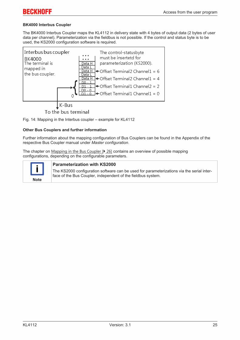
BK4000 Interbus Coupler
The BK4000 Interbus Coupler maps the KL4112 in delivery state with 4 bytes of output data (2 bytes of userdata per channel). Parameterization via the fieldbus is not possible. If the control and status byte is to beused, the KS2000 configuration software is required.
Fig. 14: Mapping in the Interbus coupler – example for KL4112
Other Bus Couplers and further information
Further information about the mapping configuration of Bus Couplers can be found in the Appendix of therespective Bus Coupler manual under Master configuration.
The chapter on Mapping in the Bus Coupler [} 26] contains an overview of possible mappingconfigurations, depending on the configurable parameters.
Note
Parameterization with KS2000The KS2000 configuration software can be used for parameterizations via the serial inter-face of the Bus Coupler, independent of the fieldbus system.

Access from the user program
KL411226 Version: 3.1
5.2 Mapping in the Bus CouplerAs already described in the Terminal Configuration section, each Bus Terminal is mapped in the BusCoupler. This mapping is usually done with the default setting in the Bus Coupler / Bus Terminal. TheKS2000 configuration software or a master configuration software (e.g. ComProfibus or TwinCAT SystemManager) can be used to change this default setting.
If the terminals are fully evaluated, they occupy memory space in the input and output process image.
The following tables provide information about how the terminals map themselves in the Bus Coupler,depending on the parameters set.
Access from the user program
KL4112 27Version: 3.1
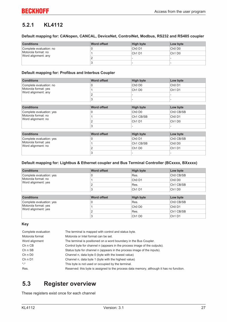
5.2.1 KL4112
Default mapping for: CANopen, CANCAL, DeviceNet, ControlNet, Modbus, RS232 and RS485 coupler
Conditions Word offset High byte Low byteComplete evaluation: noMotorola format: noWord alignment: any
0 Ch0 D1 Ch0 D01 Ch1 D1 Ch1 D02 - -3 - -
Default mapping for: Profibus and Interbus Coupler
Conditions Word offset High byte Low byteComplete evaluation: noMotorola format: yesWord alignment: any
0 Ch0 D0 Ch0 D11 Ch1 D0 Ch1 D12 - -3 - -
Conditions Word offset High byte Low byteComplete evaluation: yesMotorola format: noWord alignment: no
0 Ch0 D0 Ch0 CB/SB1 Ch1 CB/SB Ch0 D12 Ch1 D1 Ch1 D03 - -
Conditions Word offset High byte Low byteComplete evaluation: yesMotorola format: yesWord alignment: no
0 Ch0 D1 Ch0 CB/SB1 Ch1 CB/SB Ch0 D02 Ch1 D0 Ch1 D13 - -
Default mapping for: Lightbus & Ethernet coupler and Bus Terminal Controller (BCxxxx, BXxxxx)
Conditions Word offset High byte Low byteComplete evaluation: yesMotorola format: noWord alignment: yes
0 Res. Ch0 CB/SB1 Ch0 D1 Ch0 D02 Res. Ch1 CB/SB3 Ch1 D1 Ch1 D0
Conditions Word offset High byte Low byteComplete evaluation: yesMotorola format: yesWord alignment: yes
0 Res. Ch0 CB/SB1 Ch0 D0 Ch0 D12 Res. Ch1 CB/SB3 Ch1 D0 Ch1 D1
Key
Complete evaluation The terminal is mapped with control and status byte.Motorola format Motorola or Intel format can be set.Word alignment The terminal is positioned on a word boundary in the Bus Coupler.Ch n CB Control byte for channel n (appears in the process image of the outputs).Ch n SB Status byte for channel n (appears in the process image of the inputs).Ch n D0 Channel n, data byte 0 (byte with the lowest value)Ch n D1 Channel n, data byte 1 (byte with the highest value)"-" This byte is not used or occupied by the terminal.Res. Reserved: this byte is assigned to the process data memory, although it has no function.
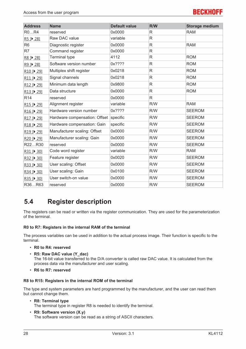
5.3 Register overviewThese registers exist once for each channel
Access from the user program
KL411228 Version: 3.1
Address Name Default value R/W Storage mediumR0…R4 reserved 0x0000 R RAMR5 [} 28] Raw DAC value variable RR6 Diagnostic register 0x0000 R RAMR7 Command register 0x0000 RR8 [} 28] Terminal type 4112 R ROM
R9 [} 28] Software version number 0x???? R ROM
R10 [} 29] Multiplex shift register 0x0218 R ROM
R11 [} 29] Signal channels 0x0218 R ROM
R12 [} 29] Minimum data length 0x9800 R ROM
R13 [} 29] Data structure 0x0000 R ROMR14 reserved 0x0000 RR15 [} 29] Alignment register variable R/W RAM
R16 [} 29] Hardware version number 0x???? R/W SEEROM
R17 [} 29] Hardware compensation: Offset specific R/W SEEROM
R18 [} 29] Hardware compensation: Gain specific R/W SEEROM
R19 [} 29] Manufacturer scaling: Offset 0x0000 R/W SEEROM
R20 [} 29] Manufacturer scaling: Gain 0x0000 R/W SEEROMR22…R30 reserved 0x0000 R/W SEEROMR31 [} 30] Code word register variable R/W RAM
R32 [} 30] Feature register 0x0020 R/W SEEROM
R33 [} 30] User scaling: Offset 0x0000 R/W SEEROM
R34 [} 30] User scaling: Gain 0x0100 R/W SEEROM
R35 [} 30] User switch-on value 0x0000 R/W SEEROMR36…R63 reserved 0x0000 R/W SEEROM
5.4 Register descriptionThe registers can be read or written via the register communication. They are used for the parameterizationof the terminal.
R0 to R7: Registers in the internal RAM of the terminal
The process variables can be used in addition to the actual process image. Their function is specific to theterminal.
• R0 to R4: reserved• R5: Raw DAC value (Y_dac)
The 16-bit value transferred to the D/A converter is called raw DAC value. It is calculated from theprocess data via the manufacturer and user scaling.
• R6 to R7: reserved
R8 to R15: Registers in the internal ROM of the terminal
The type and system parameters are hard programmed by the manufacturer, and the user can read thembut cannot change them.
• R8: Terminal typeThe terminal type in register R8 is needed to identify the terminal.
• R9: Software version (X.y)The software version can be read as a string of ASCII characters.

Access from the user program
KL4112 29Version: 3.1
• R10: Data lengthR10 contains the number of multiplexed shift registers and their length in bits.The Bus Coupler sees this structure.
• R11: Signal channelsRelated to R10, this contains the number of channels that are logically present. Thus for example ashift register that is physically present can perfectly well consist of several signal channels.
• R12: Minimum data lengthThe particular byte contains the minimum data length for a channel that is to be transferred. If the MSBis set, the control and status byte is not necessarily required for the terminal function and is nottransferred to the control, if the Bus Coupler is configured accordingly.
• R13: Data type register
Data type register Meaning0x00 Terminal with no valid data type0x01 Byte array0x02 Structure 1 byte n bytes0x03 Word array0x04 Structure 1 byte n words0x05 Double word array0x06 Structure 1 byte n double words0x07 Structure 1 byte 1 double word0x08 Structure 1 byte 1 double word0x11 Byte array with variable logical channel length0x12 Structure 1 byte n bytes with variable logical channel length (e.g. 60xx)0x13 Word array with variable logical channel length0x14 Structure 1 byte n words with variable logical channel length0x15 Double word array with variable logical channel length0x16 Structure 1 byte n double words with variable logical channel length
• R14: reserved• R15: Alignment bits (RAM)
The alignment bits are used to place the analog terminal in the Bus Coupler on a byte boundary.
R16 to R30: Manufacturer parameter area (SEEROM)
The manufacturer parameters are specific for each type of terminal. They are programmed by themanufacturer, but can also be modified by the controller. The manufacturer parameters are stored in a serialEEPROM in the terminal, and are retained in the event of voltage drop-out.
These registers can only be altered after a code word has been set in R31 [} 30].
• R17: Hardware compensation - offset (B_a)This register is used for hardware offset compensation.
• R18: Hardware compensation - gain (A_a)Gain hardware*2-16
This register is used for hardware gain compensation.0xFFFF corresponds to 1
• R19: Manufacturer scaling - offset (B_h)This register contains the offset of the manufacturer straight-line equation (equation 1.1 [} 10]). Thestraight-line equation is enabled via register R32 [} 30].
• R20: Manufacturer scaling - gain (A_h)16 bit unsigned integer*2-8 [0x0100]This register contains the scale factor of the manufacturer's equation of the straight line (Eq. 1.1 [} 10]).The straight-line equation is enabled via register R32 [} 30].1 corresponds to register value 0x0100.

Access from the user program
KL411230 Version: 3.1
R31 to R47: User parameter area (SEEROM)
The user parameters are specific for each type of terminal. They can be modified by the programmer. Theuser parameters are stored in a serial EEPROM in the terminal, and are retained in the event of voltagedrop-out. The user area is write-protected by a code word.
Note
• R31: Code word register in RAMThe code word 0x1235 must be entered here so that parameters in the user area can bemodified. If any other value is entered into this register, the write-protection is active. Whenwrite protection is not active, the code word is returned when the register is read. If thewrite protection is active, the register contains a zero value.
• R32: Feature register[0x0020]This register specifies the operation modes of the terminal.
Note
Notes about the output formatFor reasons of compatibility, 16 bits signed integer is selected as the (standard) output for-mat. The positive value range for 0 to 20 mA extends from 0 to 32767 (0x7FFF). This corre-sponds to 15 bits. Manufacturer scaling must be disabled in order to exploit all 16 bits of theterminal.
Feature bit no. Description of the operation modeBit 0 1 User scaling (R33, R34 [} 30]) active [0]Bit 1 1 Manufacturer scaling (R19, R20 [} 29]) active [1]Bit 2 0 Watchdog timer active [0]
In the delivery state, the watchdog timer is switched on. In the event of a watchdog overflow, either themanufacturer or the user switch-on value is applied to the terminal output.
Bits 3 to 7 - Reserved, don't changeBit 8 0/1 0bin: Manufacturer switch-on value [0]
1bin: User switch-on valueBits 9 to 15 - Reserved, don't change
• R33: User scaling - offset (B_w)16 bit signed integer [0x0000]This register contains the offset of the user straight-line equation (Eq. 1.4 [} 10]). The straight-lineequation is enabled via register R32 [} 30].
• R34: User scaling - gain (A_w)16 bit signed integer*2-8 [0x0100]This register contains the scaling factor of the user straight-line equation (Eq. 1.4 [} 10]). The straight-line equation is enabled via register R32 [} 30].
• R35: User switch-on value16 bit signed integer [0x0000]If the user switch-on value is enabled in register R32 [} 30], this value is applied to the terminal outputafter a system reset or a watchdog timer overflow (terminal has not received any process data for100 ms).
5.5 Control and status byteThe control and status byte is transmitted from the controller to the terminal. It can be used
• in register mode (REG = 1bin) or• in process data exchange (REG = 0bin).

Access from the user program
KL4112 31Version: 3.1
5.5.1 Process data exchange
Control byte in process data exchange (REG=0)
A gain and offset calibration of the terminal can be carried out with the control byte. The code word (0xAFFE)must be entered in R31 so that the terminal calibration can be carried out. The gain and offset of the terminalcan then be calibrated. The parameter will only be saved permanently once the code word is reset!
Bit DescriptionBit 7 0bin
Bit 6 1bin: Terminal compensation function is enabledBit 5 reservedBit 4 1bin: Gain calibrationBit 3 1bin: Offset calibrationBit 2 0bin: slow clock = 1000 ms
1bin: fast clock = 50 msBit 1 1bin: upBit 0 1bin: down
Status byte in process data exchange (REG=0)
The status byte is transferred from the terminal to the controller. In the KL4112, the status byte has nofunction for the process data exchange.

Access from the user program
KL411232 Version: 3.1
5.5.2 Register communication
Register access via process data exchange• Bit 7=1: Register mode
If bit 7 of the control byte is set, the first two bytes of the user data are not used for process dataexchange but written into the register set of the terminal or read from it.
• Bit 6=0: read, bit 6=1: writeBit 6 of the control bytes is used to specify whether a register should be read or written.
◦ Bit 6=0: A register is read without changing it. The value can be found in the input processimage.
◦ Bit 6=1: The user data are written into a register. The process is complete once the status bytein the input process image has returned an acknowledgment (see example).
• Bit 0 to 5: AddressThe address of the register to be addressed is entered in bits 0 to 5 of the control byte
Control byte in register mode (REG=1)
MSB
REG=1 W/R A5 A4 A3 A2 A1 A0
REG = 0bin: Process data exchangeREG = 1bin: Access to register structure
W/R = 0bin: Read registerW/R = 1bin: Write register
A5..A0 = register addressAddresses A5...A0 can be used to address a total of 64 registers.
Fig. 15: Register mode control byte
The control or status byte occupies the lowest address of a logical channel. The corresponding registervalues are located in the following 2 data bytes. (The BK2000 is an exception: here, an unused data byte isinserted after the control or status byte, and the register value is therefore placed on a word boundary).
Access from the user program
KL4112 33Version: 3.1
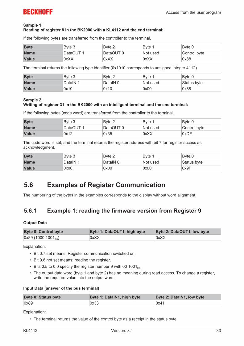
Sample 1:Reading of register 8 in the BK2000 with a KL4112 and the end terminal:
If the following bytes are transferred from the controller to the terminal,
Byte Byte 3 Byte 2 Byte 1 Byte 0Name DataOUT 1 DataOUT 0 Not used Control byteValue 0xXX 0xXX 0xXX 0x88
The terminal returns the following type identifier (0x1010 corresponds to unsigned integer 4112)
Byte Byte 3 Byte 2 Byte 1 Byte 0Name DataIN 1 DataIN 0 Not used Status byteValue 0x10 0x10 0x00 0x88
Sample 2:Writing of register 31 in the BK2000 with an intelligent terminal and the end terminal:
If the following bytes (code word) are transferred from the controller to the terminal,
Byte Byte 3 Byte 2 Byte 1 Byte 0Name DataOUT 1 DataOUT 0 Not used Control byteValue 0x12 0x35 0xXX 0xDF
The code word is set, and the terminal returns the register address with bit 7 for register access asacknowledgment.
Byte Byte 3 Byte 2 Byte 1 Byte 0Name DataIN 1 DataIN 0 Not used Status byteValue 0x00 0x00 0x00 0x9F
5.6 Examples of Register CommunicationThe numbering of the bytes in the examples corresponds to the display without word alignment.
5.6.1 Example 1: reading the firmware version from Register 9
Output Data
Byte 0: Control byte Byte 1: DataOUT1, high byte Byte 2: DataOUT1, low byte0x89 (1000 1001bin) 0xXX 0xXX
Explanation:
• Bit 0.7 set means: Register communication switched on.• Bit 0.6 not set means: reading the register.• Bits 0.5 to 0.0 specify the register number 9 with 00 1001bin.• The output data word (byte 1 and byte 2) has no meaning during read access. To change a register,
write the required value into the output word.
Input Data (answer of the bus terminal)
Byte 0: Status byte Byte 1: DataIN1, high byte Byte 2: DataIN1, low byte0x89 0x33 0x41
Explanation:
• The terminal returns the value of the control byte as a receipt in the status byte.
Access from the user program
KL411234 Version: 3.1
• The terminal returns the firmware version 0x3341 in the input data word (byte 1 and byte 2). This is tobe interpreted as an ASCII code:
◦ ASCII code 0x33 represents the digit 3◦ ASCII code 0x41 represents the letter A
The firmware version is thus 3A.
5.6.2 Example 2: Writing to an user register
Note
Code wordIn normal mode all user registers are read-only with the exception of Register 31. In orderto deactivate this write protection you must write the code word (0x1235) into Register 31. Ifa value other than 0x1235 is written into Register 31, write protection is reactivated. Pleasenote that changes to a register only become effective after restarting the terminal (power-off/power-on).
I. Write the code word (0x1235) into Register 31.
Output Data
Byte 0: Control byte Byte 1: DataOUT1, high byte Byte 2: DataOUT1, low byte0xDF (1101 1111bin) 0x12 0x35
Explanation:
• Bit 0.7 set means: Register communication switched on.• Bit 0.6 set means: writing to the register.• Bits 0.5 to 0.0 specify the register number 31 with 01 1111bin.• The output data word (byte 1 and byte 2) contains the code word (0x1235) for deactivating write
protection.
Input Data (answer of the bus terminal)
Byte 0: Status byte Byte 1: DataIN1, high byte Byte 2: DataIN1, low byte0x9F (1001 1111bin) 0xXX 0xXX
Explanation:
• The terminal returns a value as a receipt in the status byte that differs only in bit 0.6 from the value ofthe control byte.
• The input data word (byte 1 and byte 2) is of no importance after the write access. Any values stilldisplayed are invalid!
II. Read Register 31 (check the set code word)
Output Data
Byte 0: Control byte Byte 1: DataOUT1, high byte Byte 2: DataOUT1, low byte0x9F (1001 1111bin) 0xXX 0xXX
Explanation:
• Bit 0.7 set means: Register communication switched on.• Bit 0.6 not set means: reading the register.• Bits 0.5 to 0.0 specify the register number 31 with 01 1111bin.• The output data word (byte 1 and byte 2) has no meaning during read access.

Access from the user program
KL4112 35Version: 3.1
Input Data (answer of the bus terminal)
Byte 0: Status byte Byte 1: DataIN1, high byte Byte 2: DataIN1, low byte0x9F (1001 1111bin) 0x12 0x35
Explanation:
• The terminal returns the value of the control byte as a receipt in the status byte.• The terminal returns the current value of the code word register in the input data word (byte 1 and byte
2).
III. Write to Register 32 (change contents of the feature register)
Output data
Byte 0: Control byte Byte 1: DataIN1, high byte Byte 2: DataIN1, low byte0xE0 (1110 0000bin) 0x00 0x02
Explanation:
• Bit 0.7 set means: Register communication switched on.• Bit 0.6 set means: writing to the register.• Bits 0.5 to 0.0 indicate register number 32 with 10 0000bin.• The output data word (byte 1 and byte 2) contains the new value for the feature register.
CAUTION
Observe the register description!The value of 0x0002 given here is just an example! The bits of the feature register change the properties of the terminal and have a differentmeaning, depending on the type of terminal. Refer to the description of the feature registerof your terminal (chapter Register description) regarding the meaning of the individual bitsbefore changing the values.
Input data (response from the Bus Terminal)
Byte 0: Status byte Byte 1: DataIN1, high byte Byte 2: DataIN1, low byte0xA0 (1010 0000bin) 0xXX 0xXX
Explanation:
• The terminal returns a value as a receipt in the status byte that differs only in bit 0.6 from the value ofthe control byte.
• The input data word (byte 1 and byte 2) is of no importance after the write access. Any values stilldisplayed are invalid!
IV. Read Register 32 (check changed feature register)
Output Data
Byte 0: Control byte Byte 1: DataOUT1, high byte Byte 2: DataOUT1, low byte0xA0 (1010 0000bin) 0xXX 0xXX
Explanation:
• Bit 0.7 set means: Register communication switched on.• Bit 0.6 not set means: reading the register.• Bits 0.5 to 0.0 indicate register number 32 with 10 0000bin.• The output data word (byte 1 and byte 2) has no meaning during read access.

Access from the user program
KL411236 Version: 3.1
Input Data (answer of the bus terminal)
Byte 0: Status byte Byte 1: DataIN1, high byte Byte 2: DataIN1, low byte0xA0 (1010 0000bin) 0x00 0x02
Explanation:
• The terminal returns the value of the control byte as a receipt in the status byte.• The terminal returns the current value of the feature register in the input data word (byte 1 and byte 2).
V. Write Register 31 (reset code word)
Output Data
Byte 0: Control byte Byte 1: DataOUT1, high byte Byte 2: DataOUT1, low byte0xDF (1101 1111bin) 0x00 0x00
Explanation:
• Bit 0.7 set means: Register communication switched on.• Bit 0.6 set means: writing to the register.• Bits 0.5 to 0.0 specify the register number 31 with 01 1111bin.• The output data word (byte 1 and byte 2) contains 0x0000 for reactivating write protection.
Input Data (answer of the bus terminal)
Byte 0: Status byte Byte 1: DataIN1, high byte Byte 2: DataIN1, low byte0x9F (1001 1111bin) 0xXX 0xXX
Explanation:
• The terminal returns a value as a receipt in the status byte that differs only in bit 0.6 from the value ofthe control byte.
• The input data word (byte 1 and byte 2) is of no importance after the write access. Any values stilldisplayed are invalid!

Appendix
KL4112 37Version: 3.1
6 Appendix
6.1 Support and ServiceBeckhoff and their partners around the world offer comprehensive support and service, making available fastand competent assistance with all questions related to Beckhoff products and system solutions.
Beckhoff's branch offices and representatives
Please contact your Beckhoff branch office or representative for local support and service on Beckhoffproducts!
The addresses of Beckhoff's branch offices and representatives round the world can be found on her internetpages:http://www.beckhoff.com
You will also find further documentation for Beckhoff components there.
Beckhoff Headquarters
Beckhoff Automation GmbH & Co. KG
Huelshorstweg 2033415 VerlGermany
Phone: +49(0)5246/963-0Fax: +49(0)5246/963-198e-mail: [email protected]
Beckhoff Support
Support offers you comprehensive technical assistance, helping you not only with the application ofindividual Beckhoff products, but also with other, wide-ranging services:
• support• design, programming and commissioning of complex automation systems• and extensive training program for Beckhoff system components
Hotline: +49(0)5246/963-157Fax: +49(0)5246/963-9157e-mail: [email protected]
Beckhoff Service
The Beckhoff Service Center supports you in all matters of after-sales service:
• on-site service• repair service• spare parts service• hotline service
Hotline: +49(0)5246/963-460Fax: +49(0)5246/963-479e-mail: [email protected]
List of illustrations
KL411238 Version: 3.1
List of illustrationsFig. 1 KL4112 ........................................................................................................................................ 8Fig. 2 Spring contacts of the Beckhoff I/O components......................................................................... 11Fig. 3 Attaching on mounting rail ........................................................................................................... 12Fig. 4 Disassembling of terminal............................................................................................................ 13Fig. 5 Power contact on left side............................................................................................................ 14Fig. 6 Standard wiring............................................................................................................................ 16Fig. 7 Pluggable wiring .......................................................................................................................... 16Fig. 8 High Density Terminals................................................................................................................ 16Fig. 9 Connecting a cable on a terminal point ....................................................................................... 17Fig. 10 KL4112 - connection and LEDs ................................................................................................... 19Fig. 11 KS2000 configuration software.................................................................................................... 22Fig. 12 Mapping in the Lightbus coupler – example for KL4112.............................................................. 24Fig. 13 Mapping in the Profibus coupler – example for KL4112 .............................................................. 24Fig. 14 Mapping in the Interbus coupler – example for KL4112 .............................................................. 25Fig. 15 Register mode control byte.......................................................................................................... 32