
DLP5531-Q1 Chipset Video Processing for Light Control ...
29
1 DLPA101 – October 2018 Submit Documentation Feedback Copyright © 2018, Texas Instruments Incorporated DLP5531-Q1 Chipset Video Processing for Light Control Applications Application Report DLPA101 – October 2018 DLP5531-Q1 Chipset Video Processing for Light Control Applications Tristan Garcia ABSTRACT This application report describes the video processing performed by the DLPC230-Q1 as part of the DLP5531-Q1 chipset to display an image optimized for automotive light control applications such as high resolution headlights and other exterior lighting products. Topics include image sequencing, illumination driving architecture, dithering, gamma correction, and image resizing which all impact the final output image. This information is intended for system designers involved in video content generation and illumination design. TI applications engineers and software tools typically configure the parameters required to optimally display video in automotive light control end applications. However, an understanding of these background concepts can benefit designers working with the DLP ® Products chipset. Contents 1 DMD Imaging Introduction .................................................................................................. 3 2 Typical DLP5531-Q1 Chipset Block Diagram ............................................................................ 4 3 DLPC230-Q1 Processing Path Overview................................................................................. 5 4 DMD Sequencing ............................................................................................................ 7 5 Video Processing ........................................................................................................... 18 6 Pixel Mapping and Image Resizing ...................................................................................... 23 List of Figures 1 DMD Projection .............................................................................................................. 3 2 Typical System Block Diagram ............................................................................................ 4 3 System Block Diagram ...................................................................................................... 5 4 Video Latency ................................................................................................................ 6 5 Sequence Example Input Image........................................................................................... 7 6 4-bit Brightness Intensity Levels ........................................................................................... 7 7 Sequence Example Bit Planes ............................................................................................. 8 8 Sequence Example Bit Weights ........................................................................................... 9 9 Bit Segments................................................................................................................ 11 10 Reduced Bit Segments .................................................................................................... 11 11 Increased Bit Segments ................................................................................................... 11 12 Optimized Illumination Time .............................................................................................. 12 13 Unoptimized Illumination Time ........................................................................................... 13 14 DMD Duty Cycle............................................................................................................ 13 15 Illumination Driver Timing Diagram ...................................................................................... 15 16 Recommended LED Driver Block Diagram ............................................................................. 16 17 Example Sequence Timing ............................................................................................... 17 18 Dithering vs Rounding ..................................................................................................... 18 19 Dithering Process .......................................................................................................... 19 20 Dithering at Pixel-Level .................................................................................................... 20
Transcript of DLP5531-Q1 Chipset Video Processing for Light Control ...

1DLPA101–October 2018Submit Documentation Feedback
Copyright © 2018, Texas Instruments Incorporated
DLP5531-Q1 Chipset Video Processing for Light Control Applications
Application ReportDLPA101–October 2018
DLP5531-Q1 Chipset Video Processing for Light ControlApplications
Tristan Garcia
ABSTRACTThis application report describes the video processing performed by the DLPC230-Q1 as part of theDLP5531-Q1 chipset to display an image optimized for automotive light control applications such as highresolution headlights and other exterior lighting products. Topics include image sequencing, illuminationdriving architecture, dithering, gamma correction, and image resizing which all impact the final outputimage. This information is intended for system designers involved in video content generation andillumination design.
TI applications engineers and software tools typically configure the parameters required to optimallydisplay video in automotive light control end applications. However, an understanding of these backgroundconcepts can benefit designers working with the DLP® Products chipset.
Contents1 DMD Imaging Introduction .................................................................................................. 32 Typical DLP5531-Q1 Chipset Block Diagram ............................................................................ 43 DLPC230-Q1 Processing Path Overview................................................................................. 54 DMD Sequencing ............................................................................................................ 75 Video Processing........................................................................................................... 186 Pixel Mapping and Image Resizing ...................................................................................... 23
List of Figures
1 DMD Projection .............................................................................................................. 32 Typical System Block Diagram ............................................................................................ 43 System Block Diagram...................................................................................................... 54 Video Latency ................................................................................................................ 65 Sequence Example Input Image........................................................................................... 76 4-bit Brightness Intensity Levels ........................................................................................... 77 Sequence Example Bit Planes............................................................................................. 88 Sequence Example Bit Weights ........................................................................................... 99 Bit Segments................................................................................................................ 1110 Reduced Bit Segments .................................................................................................... 1111 Increased Bit Segments ................................................................................................... 1112 Optimized Illumination Time .............................................................................................. 1213 Unoptimized Illumination Time ........................................................................................... 1314 DMD Duty Cycle............................................................................................................ 1315 Illumination Driver Timing Diagram ...................................................................................... 1516 Recommended LED Driver Block Diagram ............................................................................. 1617 Example Sequence Timing ............................................................................................... 1718 Dithering vs Rounding ..................................................................................................... 1819 Dithering Process .......................................................................................................... 1920 Dithering at Pixel-Level .................................................................................................... 20

www.ti.com
2 DLPA101–October 2018Submit Documentation Feedback
Copyright © 2018, Texas Instruments Incorporated
DLP5531-Q1 Chipset Video Processing for Light Control Applications
21 Gamma Curve Linear Function........................................................................................... 2122 Gamma Curve Power Function .......................................................................................... 2223 Diamond and Orthogonal Pixels ......................................................................................... 2324 DLP5531-Q1 DMD Array.................................................................................................. 2425 DLP5531-Q1 DMD Array Columns ...................................................................................... 2526 DLP5531-Q1 DMD Array Rows .......................................................................................... 2627 Scaling 2:1 Video Input.................................................................................................... 2628 Diamond Pixel Diagonal Lines 1 Pixel................................................................................... 2729 Diamond Pixel Diagonal Lines 4 Pixels ................................................................................. 27
List of Tables
1 4-Bit Binary Bit Weights..................................................................................................... 82 Bit Weight Examples....................................................................................................... 103 Illumination Driver Timing ................................................................................................. 154 Resolution Resizing Examples ........................................................................................... 28
TrademarksDLP Composer is a trademark of Texas Instruments.DLP is a registered trademark of Texas Instruments.All other trademarks are the property of their respective owners.
Light SourceLight Absorber
Projection Lens
www.ti.com DMD Imaging Introduction
3DLPA101–October 2018Submit Documentation Feedback
Copyright © 2018, Texas Instruments Incorporated
DLP5531-Q1 Chipset Video Processing for Light Control Applications
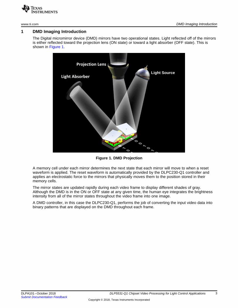
1 DMD Imaging IntroductionThe Digital micromirror device (DMD) mirrors have two operational states. Light reflected off of the mirrorsis either reflected toward the projection lens (ON state) or toward a light absorber (OFF state). This isshown in Figure 1.
Figure 1. DMD Projection
A memory cell under each mirror determines the next state that each mirror will move to when a resetwaveform is applied. The reset waveform is automatically provided by the DLPC230-Q1 controller andapplies an electrostatic force to the mirrors that physically moves them to the position stored in theirmemory cells.
The mirror states are updated rapidly during each video frame to display different shades of gray.Although the DMD is in the ON or OFF state at any given time, the human eye integrates the brightnessintensity from all of the mirror states throughout the video frame into one image.
A DMD controller, in this case the DLPC230-Q1, performs the job of converting the input video data intobinary patterns that are displayed on the DMD throughout each frame.

VBATT
Fla
sh
TPS99000-Q1
Power sequencing
and monitoring
System Diagnostics:
external watchdogs
and other monitors
1.1V1.8V3.3V
LED
drive
DLPC230-Q1
eSRAM
frame buffer
MPU
Power
Regulation
Control &
Monitor
Image Scaling
Sub-LVDS
DMD Power
GPIO
(configurable)
ADC Control
Reset &
Power Good
6.5V
Photodiode
SPI
Internal
Control
External
Monitor
SPI
Host
SPI
HOST
IRQ
OpenLDI
24-bit RGB
& Syncs
Flash
SPI
PROJ_ON
DMD Power
Regulation
I2C
TMP411
I2C
DLP5531-Q1
LED
Control
ADC Measurements
Typical DLP5531-Q1 Chipset Block Diagram www.ti.com
4 DLPA101–October 2018Submit Documentation Feedback
Copyright © 2018, Texas Instruments Incorporated
DLP5531-Q1 Chipset Video Processing for Light Control Applications
2 Typical DLP5531-Q1 Chipset Block DiagramThe DLP5531-Q1 chipset includes three components: DLP5531-Q1, DLPC230-Q1, and TPS99000-Q1. Atypical automotive exterior lighting block diagram is shown in Figure 2. The DLP5531-Q1 is a 0.55" 1.3megapixel DMD. The DLPC230-Q1 processes video input and commands from a host processor, andthen drives the DLP5531-Q1 DMD and illumination source based on these inputs. The TPS99000-Q1includes power regulators for the DMD voltage rails, and helps to coordinate power-up and power-downfor the chipset. It also includes an ADC measurement sub-system that is controlled by the DLPC230-Q1 tomonitor system voltages such as input voltage rails.
Figure 2. Typical System Block Diagram

MPUHOST_I2C
HOST_SPI
GPIO (31:0)
Parallel Video Port 28Test
Pattern Generator
Clocks & Reset Generation
Real Time Control System
SRAM(Frame Memory)
DMD_High Speed 0 Diff. PortDMD_High Speed 1 Diff. Port
SplashScreen
Clock (Crystal)Reset Control
12KB Startup
Boot ROM
Input Control
Processing
HW CMD
ASSIST
PMIC_AD3
OpenLDI Port (5 lanes) 10
10OpenLDI Port (5 lanes)
DMD Low Speed Port
DLP® Display Formatting
DMD I/F
- Dynamic Scaling - Gamma Correction - Dithering
Video Processing
www.ti.com DLPC230-Q1 Processing Path Overview
5DLPA101–October 2018Submit Documentation Feedback
Copyright © 2018, Texas Instruments Incorporated
DLP5531-Q1 Chipset Video Processing for Light Control Applications
3 DLPC230-Q1 Processing Path OverviewFigure 3 shows a block diagram of the internal blocks of the DLPC230-Q1. This document focuses on theyellow highlighted blocks which are related to the processing and displaying of video data.
Figure 3. System Block Diagram
The video path begins with either external video input or internal image generation. The DLPC230-Q1supports both OpenLDI (FPD-Link I) and parallel external video input. It also includes support for basicstatic test pattern generation and static splash images loaded from flash memory. These sources aremultiplexed into the video processing block.
The video processing block performs real-time image scaling, corrects for gamma, and applies dithering.The output of the video processing is input to the formatter block to convert the image to DMD data. Theformatter block includes the sequencer that breaks the image down into DMD mirror positions for display.Output data from the formatter block is then written to the DMD over its high speed and low speed ports.Signals are also output to drive illumination synchronously with DMD events throughout the video frame.
3.1 Video InputThe DLPC230-Q1 supports RGB888 video input, where each color has 8 bits per pixel. For the headlightapplication, the DLPC230-Q1 only uses 8-bit red data from any video source. Blue and green data areunused. It is recommended that blue and green inputs be set to zero in order to avoid unnecessary powerconsumption.
The DLPC230-Q1 parallel video input interface supports signal multiplexing to map any bit to any bit. Thiscan be configured in the DLP Composer™ for Automotive tool. This tool includes help documentation toexplain the usage of this interface. This allows the use of any color signals on the parallel interface as longas they are mapped to the red data. Other unused parallel data signals on the DLPC230 may be tied toground.
The DLPC230-Q1 OpenLDI interface supports signal multiplexing for data lanes, but individual color datacannot be multiplexed. Therefore, all data lanes must be connected and the video data must be inputthrough the red data bits.
Refer to the DLPC230-Q1 data sheet for specifications on video timing, supported resolutions, andsupported frame rates.

Frame 1
Frame 1
Frame 2
Frame 2
Frame 3
Frame 3
DLPC230-Q1 Input Video
DLP5531-Q1 Display
DLPC230-Q1 Processing Path Overview www.ti.com
6 DLPA101–October 2018Submit Documentation Feedback
Copyright © 2018, Texas Instruments Incorporated
DLP5531-Q1 Chipset Video Processing for Light Control Applications
3.2 Video LatencyThe video latency of the DLP5531-Q1 chipset is one video frame. This is the time that it takes for theDLPC230-Q1 to receive the video data, process it, and display it on the DLP5531-Q1 DMD. A typicalvideo input frame rate is 60 Hz, which is 16.66 ms.
Figure 4. Video Latency

0 0 0 0 0000
0 0 0 1 0001
0 0 1 0 0010
0 0 1 1 0011
0 1 0 0 0100
0 1 0 1 0101
0 1 1 0 0110
0 1 1 1 0111
1 0 0 0 1000
1 0 0 1 1001
1 0 1 0 1010
1 0 1 1 1011
1 1 0 0 1100
1 1 0 1 1101
1 1 1 0 1110
1 1 1 1 1111
www.ti.com DMD Sequencing
7DLPA101–October 2018Submit Documentation Feedback
Copyright © 2018, Texas Instruments Incorporated
DLP5531-Q1 Chipset Video Processing for Light Control Applications
4 DMD SequencingThe goal of DMD sequencing is to coordinate the two DMD mirror states over time to create a full bitdepth image ranging from full dark (black) to full bright (white). A sequence is a look-up table programmedto SPI flash and read by the DLPC230-Q1. This look-up table defines how the DLPC230-Q1 will convertinput video data to DMD instructions. The DLPC230-Q1 performs the actions in this table on each inputvideo frame to properly display it. The sequence also defines the illumination control signals throughoutthe video frame in order to synchronize the illumination with DMD positions.
The following sections use an example to demonstrate how sequencing works and then describeindividual aspects in further detail.
4.1 Introduction ExampleThe following simplified example demonstrates how the two states of the DMD can be utilized to achieve abroad range of brightness intensities. In this example, a gray ramp image with 4 bits of depth is displayedas shown in Figure 5.
Figure 5. Sequence Example Input Image
With a basic binary bit depth of 4, there are 24 = 16 possible brightness intensities.
Figure 6. 4-bit Brightness Intensity Levels
Since the DMD is a binary device, the DMD mirrors cannot directly display these intermediate values.Pulse width modulation is used to create intermediate intensity levels. The DLPC230-Q1 breaks the imageinto individual bit patterns of ON or OFF data, referred to as bit planes. It then transmits each of these bitplanes to the DMD in rapid succession.

Original Image
Bit 0
Bit 1
Bit 2
Bit 3
DMD Sequencing www.ti.com
8 DLPA101–October 2018Submit Documentation Feedback
Copyright © 2018, Texas Instruments Incorporated
DLP5531-Q1 Chipset Video Processing for Light Control Applications
Figure 7 shows what these bit planes would look like given the example input video data and bit depthdescribed above. The white regions are ON micromirrors and the black regions are OFF micromirrors.
Figure 7. Sequence Example Bit Planes
This representation shows the white portions at the same intensity for each bit plane, but each bit planemust have different white intensity to represent different binary weights. Bit 0 must have half the intensityof bit 1, and bit 1 must have half the intensity of bit 2:
Table 1. 4-Bit Binary Bit Weights
Bit Plane Relative Bit Weight0 11 22 43 8
If these 4 bit planes were added on top of each other with the correct bit weight, the original image wouldbe created.
There are two mechanisms for controlling the bit weight of each bit plane: time displayed and illuminationmagnitude. For the purposes of DLPC230-Q1 sequences, illumination magnitude is kept constantthroughout the frame to simplify the illumination driver electronics. Therefore, time is the only mechanismused to control bit weight. The eye integrates the displayed image, which means that a bit plane that isdisplayed for a longer period of time will be perceived with a greater intensity.

Original Image
Bit 3 Bit 2 Bit 1 Bit 0
Bit 3 Bit 2 Bit 1 Bit 0
Video Frame Time
www.ti.com DMD Sequencing
9DLPA101–October 2018Submit Documentation Feedback
Copyright © 2018, Texas Instruments Incorporated
DLP5531-Q1 Chipset Video Processing for Light Control Applications
Figure 8 demonstrates one way in which the bit planes could be displayed within the video frame tomaintain their respective bit weights. Each block of time in the video frame indicates the time over whichthe DMD is displaying that bit plane. The time of each consecutive bit is halved in order to maintain thecorrect bit weights. The bit plane images are displayed with the bit weight that the eye will perceive basedon time displayed. The end-user’s eye will only perceive the final image shown at the bottom of Figure 8 ifthese bit planes are displayed at high speed. Intuitively, it is clear that the far left side of the original rampis a pixel value of 0, and indeed the left side of each bit plane sets the micromirrors in an OFF state.Likewise, the right side of the original ramp is a pixel value of 1, and the right side of each bit plane setsthe micromirrors to an ON state.
Figure 8. Sequence Example Bit Weights
The sequence look-up table defines the number of bit planes used in a video frame, the bit weights, andtiming of the bits to be displayed. During operation, the DLPC230-Q1 uses that look-up table and applies itto break down and display any arbitrary video content that is provided.
4.2 Sequence DefinitionsThis section describes commonly used terms in sequence generation. Additional implementation detailbeyond the introduction example is also provided.
4.2.1 Bit PlaneA bit plane is the binary state of all of the DMD mirrors required to represent a specific bit in the sequence.At any displaying point within the video frame, all of the DMD mirrors are displaying one specific bit plane.The number of bit planes used in a sequence varies, as do the bit weights of those bit planes. The mirrorstates within a bit plane are entirely dependent on the sequence definition and the input image content,which often varies every frame.
4.2.2 Complement Bit PlaneA complement bit plane is the inverse data of a specified bit plane. All ON mirrors in the bit plane are OFFand all OFF mirrors in the bit plane are ON when the complement bit plane is displayed. The use ofcomplement bit planes is discussed further in Section 4.3.3.

DMD Sequencing www.ti.com
10 DLPA101–October 2018Submit Documentation Feedback
Copyright © 2018, Texas Instruments Incorporated
DLP5531-Q1 Chipset Video Processing for Light Control Applications
4.2.3 Bit WeightBit weight is the relative intensity of each bit plane. This directly impacts the bit depth, and typically bitdepth is used to summarize the bit weights used. Note that different bit weights are used for differentsequences for optimization of brightness, which means that each sequence may have slightly different bitdepth.
4.2.4 Bit DepthBit depth is a single number used to describe the range of intensities that are capable of being displayedbased on the selected bit weights in the sequence. For example, a bit depth of 8 means that 28 = 256unique intensities can be displayed with assumed binary weighting.
The DLPC230-Q1 is capable of using non-binary bit weights, and is almost always programmed to do sofor optimal displaying.
As an example, the weights in Table 2 can be used.
Table 2. Bit Weight Examples
Bit Plane Relative Bit Weight0 11 12 23 24 45 46 67 68 89 8
The bit depth for these bits is still represented in the form 2BitDepth despite their non-binary weighting. Tocalculate this, the following formula is used:
(1)
In this example, the least significant bit (LSb) is 1 and the sum of all bit weights is 42. Therefore the bitdepth using these example bit weights is 5.39.
Using the same bit weight multiple times means that some intensity levels can be generated with severaldifferent combinations of bit planes. This allows the DLPC230-Q1 to adjust which bit planes are used tocreate each pixel’s intensity in real time. The benefit to this is to spread the frequency at which each pixelis illuminated across the video frame time. This is one mechanism used to reduce potential low frequencyflickering that could be perceived by the eye.
Increasing the bit depth is usually a tradeoff with other parameters in the sequence, such as brightness.This is discussed further in Section 4.3.1.
4.2.5 Bit SegmentA bit segment is a time span in the sequence during which a bit plane is displayed on the DMD.
As mentioned in the introduction example, each bit plane must be displayed for a specific amount of timeto achieve its relative bit weight compared to the other bit planes. However, this time does not have to bedisplayed all at once. It is preferable to split the time required for a bit plane into several bit segments anddistribute them across the sequence rather than display the bit plane in one long continuous interval. Thisis done to avoid low frequency switching artifacts that could be perceived by the end-user when displayingcertain intensity levels.
Figure 9 uses the simplified introduction example 4-bit sequence to demonstrate how bit segments can beused to distribute the bit weights across the sequence time.

Bit 3 Bit 3Bit 3 Bit 3Bit 3 Bit 3Bit 3 Bit 3Bit 2 Bit 2Bit 2 Bit 2Bit 1Bit 1 Bit 0
1 1 1 1 1 1 1 10 0 0 0 0 0 0DMD Mirror State
while displaying
half intensity
Bit Segments
Video Frame Time
Bit 3 Bit 2 Bit 1 Bit 0
Video Frame Time
0 0 0
DMD Mirror State
while displaying
half intensity
Bit Segments
Bit 3 Bit 2 Bit 1 Bit 0
Video Frame Time
Bit 3 Bit 3 Bit 3 Bit 3 Bit 3 Bit 3 Bit 3 Bit 3 Bit 2 Bit 2 Bit 2 Bit 2 Bit 1 Bit 1 Bit 0
Bit 3 Bit 3Bit 3 Bit 3Bit 3 Bit 3Bit 3 Bit 3Bit 2 Bit 2Bit 2 Bit 2Bit 1Bit 1 Bit 0
www.ti.com DMD Sequencing
11DLPA101–October 2018Submit Documentation Feedback
Copyright © 2018, Texas Instruments Incorporated
DLP5531-Q1 Chipset Video Processing for Light Control Applications
Figure 9. Bit Segments
In the top sequence each bit plane is only displayed once and bit 3 consumes half of the frame time. If ahalf intensity shade (b1000) were to be displayed on a micromirror, that micromirror would only be onduring the bit 3 time segment. This would cause the frequency of light switching from that micromirror tobe exactly the frame rate as shown in Figure 10.
Figure 10. Reduced Bit Segments
If the same half intensity were displayed on the bottom sequence, the frequency of light switching wouldbe much higher, which is more desirable to avoid any perceived brightness switching or strobing effects.This is demonstrated in Figure 11.
Figure 11. Increased Bit Segments
4.2.6 Reset WaveformThe DMD reset waveform is a voltage pulse that the DLPC230-Q1 commands the DLP5531-Q1 toexecute after each bitplane is loaded to the DMD during the video frame. This pulse applies anelectrostatic force to each micromirror in the DMD array in order to move them to the position loaded intotheir memory cells.
4.2.7 Refresh RateThe human eye will integrate 60 Hz smoothly when viewing stable content, but moving content inapplications such as automotive headlights adds the risk of viewing only small time portions of the totalvideo frame. This can cause brightness flickering artifacts unless a higher refresh rate is used.
Refresh rate is the frequency at which the same content is repeatedly displayed. Increasing the refreshrate mitigates flicker and PWM artifacts. A faster refresh rate is achieved using bit segments to distributethe display of bit planes into several groups within the video frame. Generally the refresh rate is an integermultiple of the video frame rate. For example, if the bit planes are segmented and separated into 6 groupsin a 60-Hz frame rate sequence, then the refresh rate is 360 Hz.

Bit 0 Display
Min reset-to-reset
RR Bit 1 Display
Illumination
Enable
DMD Sequencing www.ti.com
12 DLPA101–October 2018Submit Documentation Feedback
Copyright © 2018, Texas Instruments Incorporated
DLP5531-Q1 Chipset Video Processing for Light Control Applications
In the bit segment example in Figure 10 with poorly optimized bit 3 length, if the user stops viewing theprojection source halfway through the video frame then the user may perceive bit 3 as the entire intensityof the video frame. If the user then begins viewing halfway through another frame, they may only see bit 2,1, 0, which are all off. This large brightness difference can cause flickering effects as the user andprojection source move relative to each other, or when the user blinks for example. This effect is alsomore noticeable in peripheral vision. Designing for a higher refresh rate averages the content at a higherfrequency to mitigate any potential perceived flickering effect.
When refresh rate is increased, each bit segment becomes shorter, which also helps mitigate potentialPWM artifacts from low frequency switching.
4.2.8 Sub-FrameA sub-frame is one set of bit segments used to display the video content within the video frame. Thenumber of sub-frames is determined by the refresh rate. For example, if the refresh rate is 360 Hz and theframe rate is 60 Hz, then there are 6 sub-frames. This number of sub-frames is typical of the sequencesused for automotive exterior lighting applications.
4.3 Key ParametersSeveral key factors impact application-specific sequence design. Headlight sequences utilize single-colorillumination and prioritize brightness and refresh rate. Other parameters that are considered are DMDmicromirror landed duty cycle, number of DMD reset waveform executions, and bit depth.
4.3.1 BrightnessBrightness is the highest sequence priority for the headlight application. Maximum brightness is achievedby minimizing the time that light is off in the sequence.
There are 3 situations when light may be off during a sequence:• Reduced DMD duty cycle at high temperature for extended automotive operating lifetime• DMD reset waveform executions to change mirror positions• Illumination time shorter than the DMD load time
DMD duty cycle is described in further detail in Section 4.3.3.
DMD resets are described in further detail in Section 4.3.4.
Illumination Time and DMD Load time are described in further detail in Section 4.3.2.
4.3.2 Illumination Time and DMD Load TimeIllumination time shorter than the DMD load time can be avoided by selecting the bit weights in a way thatavoids any bit segment from requiring less display time than the DMD load time. Ultimately this results intrading bit depth with brightness. For the headlight application, brightness is prioritized and sequences aredesigned to prevent any illumination time from being shorter than the DMD load time. The minimum reset-to-reset time for the DLP5531-Q1 chipset is approximately 105 μs. This minimum length is determined bythe DMD loading and reset time.
Figure 12 demonstrates a bit segment that displays for longer than the minimum reset to reset time. Thisis the ideal scenario for the headlight application because the light output is maximized.
Figure 12. Optimized Illumination Time

99/1
50/50
Sub-Frame
Illumination ON except during resets
DMD Displaying Video Data
Illumination OFF
DMD Displaying Inverted Video Data
Sub-Frame
Video Frame
Min reset-to-reset
Bit 0 Display RR Bit 1 Display
Illumination
Enable
Dark time
Not typical for headlight sequences
www.ti.com DMD Sequencing
13DLPA101–October 2018Submit Documentation Feedback
Copyright © 2018, Texas Instruments Incorporated
DLP5531-Q1 Chipset Video Processing for Light Control Applications
Figure 13 demonstrates a bit segment that must display for less time than the minimum reset to resettime. This could occur if the relative bit weight of bit 0 to bit 1 forces bit 0 to be displayed for too short of atime, for example. In this scenario, the illumination must be disabled while the remaining DMD data isloaded for bit 1. This early disable of the illumination signal results in additional light loss. If bit 0 continuedto be illuminated until the loading completed, the intensity of bit 0 would be too high compared to bit 1 andsome pixel levels would appear too bright.
Figure 13. Unoptimized Illumination Time
Again, this scenario is typically avoided entirely for the headlight application by optimizing bit depth andthe number of bit segments used in the sequence.
4.3.3 DMD Micromirror Duty CycleDMD micromirror duty cycle defines the percentage of time that a micromirror is in the ON state. Thispercentage is content-dependent as demonstrated in the previous sequence examples, and can vary foreach micromirror on the DMD in the same frame based on what that micromirror is displaying.
Sequence duty cycle is commonly referred to as an ON/OFF value, and defines the percentage of timethat the DMD is displaying content. The specified ON time includes reset waveform executions betweenON bit segments. Light must be off during the reset waveform execution since the micromirrors aremoving to their next state during this time and system contrast would be impacted by this scattered light.Illumination drive timing is defined in more detail in Section 4.4. During the OFF time, illumination isdisabled and inverse video data is loaded to the DMD to exercise the DMD mirrors. This inverse dataduring OFF time is referred to as a complement bit plane.
Sequences are designed with a specific duty cycle that is designed to limit the maximum DMD micromirrorduty cycle in order to maximize lifetime of the device over its wide automotive temperature range.Reliability and time for duty cycle operation is beyond the scope of this document, and may be found inReliability Lifetime Estimates for DLP553x-Q1.
While operating at a lower duty cycle may be used to maximize the lifetime of the DMD, the tradeoff foroperating at a lower duty cycle is brightness.
Two example DMD duty cycles are shown in Figure 14. This view shows sub-frames, each of whichincludes several bit segments. Several DMD resets occur within each sub-frame for each bit segmentdisplayed. Illumination duty cycle will be lower than the DMD duty cycle because of the additional light lossfrom reset time.
Figure 14. DMD Duty Cycle

DMD Sequencing www.ti.com
14 DLPA101–October 2018Submit Documentation Feedback
Copyright © 2018, Texas Instruments Incorporated
DLP5531-Q1 Chipset Video Processing for Light Control Applications
Any integer DMD duty cycle from 99% ON to 50% ON can be supported.
4.3.4 Number of ResetsThe DMD reset waveform is a fixed amount of time required to move the mirrors to their new positions.The number of times that the reset waveform is executed in a sequence is determined by the number ofbit planes and the number of bit segments per bit plane. For the headlight application, this is directlyrelated to bit depth and refresh rate. Doubling refresh rate will typically double the number of resetwaveform executions. Adding one extra bit of depth will also typically double the number of resetwaveform executions. These are general guidelines used when developing sequences, and there areexceptions.
Generally the reset waveform is executed 50-100 times per frame in a headlight sequence.
The tradeoff for adding additional reset waveform executions to the sequence is that illumination must beoff during this time.
4.3.5 Refresh RateRefresh rate is defined in Section 4.2.7. For headlight applications, sequences are typically designed for360 Hz when using 60-Hz frame rate. This means that the content is displayed approximately 6 times pervideo frame. The maximum refresh rate varies with duty cycle and bit depth, but a typical maximum is 720Hz for high duty cycle, low bit depth sequences while minimizing light loss.
4.3.6 Bit DepthBit depth is defined in Section 4.2.4. For headlight applications, sequences are typically designed forapproximately 5.0-6.0 bits of depth. The DLPC230-Q1 accepts video input with exactly 8 binary bits ofdepth regardless of sequence bit depth. The video depth is then mapped to output bit depth using thesequence and other algorithms described in this document.
Note that this bit depth value only considers sequence bit weights. The perceived system bit depth ismuch greater than this specified bit depth because of dithering and gamma curve correction described inSection 5.1 and Section 5.2.
4.4 Illumination DriverThe sequence controls when illumination signals are enabled in order to synchronize illumination withDMD reset waveform executions. The sequence bit weights and illumination signals are timed assumingideal square pulses of light. Of course it is not possible to disable illumination instantaneously, and anyrise and fall time changes the intensity of the weights. The intensity change due to rise and fall times canbe perceived as non-linear pixel intensity if it is too significant. This section describes the recommendeddriver architecture and timing in order to achieve accurate bit weights.
There are two illumination signals driven by the DLPC230-Q1 for headlight sequences: drive controlenable and shunt control enable. These two signals can be mapped to any of the four DLPC230-Q1LEDSEL_X pins using the DLP Composer for Automotive tool. By convention, LEDSEL_0 and LEDSEL_3are used for drive control enable and shunt control enable, respectively.
The drive control enable is intended to be used as a current drive signal. The shunt control enable signalcan be used as a way to quickly redirect current away from LEDs in order to reduce rise and fall timebetween bit segments. With the use of a shunt signal, it is not necessary to completely disable the drivecurrent during the reset waveform and OFF duty cycle time as long as the current does not flow throughthe LED.

Drive Control
Enable
Shunt Control
Enable
LED current
TrTf
DMD
Reset
OFF Duty
CycleON Duty Cycle
ON Duty
Cycle
ON
Duty
Cycle
Tsrd Tsfd
Tdfd Tdrd
TsfdTsrd
www.ti.com DMD Sequencing
15DLPA101–October 2018Submit Documentation Feedback
Copyright © 2018, Texas Instruments Incorporated
DLP5531-Q1 Chipset Video Processing for Light Control Applications
4.4.1 Illumination Drive TimingFigure 15 and Table 3 describe the recommended timing for LED current relative to the illumination controlsignals in order to maintain correct bit weights in the sequence. During the DMD reset waveform the drivecontrol enable is kept high to maintain current within the driver control loop for this short period of time.The shunt is enabled during this time so that the current bypasses the LEDs. During DMD OFF duty cycle,the drive control enable is set low and the shunt control enable is set high. The DLP Composer forAutomotive tool allows adjustment of the drive control enable and shunt control enable signal timing toaccount for rise and fall time delays in the driver architecture. These delays can be used to align the LEDcurrent rise and fall time with the sequence events.
Figure 15. Illumination Driver Timing Diagram
Table 3. Illumination Driver Timing
PARAMETER DESCRIPTION MIN MAX
TfRecommended falling edge time of LED current fromstart of sequence event. 2 μs
TrRecommended rising edge time of LED current from endof sequence event. 2 μs
TsrdShunt enable rising edge delay from sequence event.Positive value enables shunt prior to sequence event.
Timing configurable in DLP Composer™ for Automotivetool to account for driver-specific delay time.
TsfdShunt enable falling edge delay from sequence event.Positive value disables shunt prior to sequence event.
Tdfd
Drive enable falling edge delay from sequence event.Positive value disables drive enable prior to sequenceevent.
Tdrd
Drive enable rising edge delay from sequence event.Positive value enables drive enable prior to sequenceevent.

Controller
Shunt Control
Enable
Power
Minimize
loop size
ENDrive Control
Enable
DMD Sequencing www.ti.com
16 DLPA101–October 2018Submit Documentation Feedback
Copyright © 2018, Texas Instruments Incorporated
DLP5531-Q1 Chipset Video Processing for Light Control Applications
4.4.2 Recommended Illumination Driver ArchitectureFigure 16 shows a recommended LED driver architecture to use these signals. A buck regulator, such asthe TI LM3409 is controlled by the drive control enable signal. A FET is controlled by shunt control enableto quickly shunt current away from the LED. The length of the FET and LED loop should be minimized inorder to minimize electromagnetic interference since a high current is switching between these two paths.This may involve minimizing cable length to the LED, or placing the FET on the same board as the LED.
Figure 16. Recommended LED Driver Block Diagram
4.5 ADC Measurement SynchronizationIn addition to illumination control signals, the DLPC230-Q1 sequences also include a trigger signal forADC measurement capture. The ADC measurements are captured using the TPS99000-Q1 and reportedback to the DLPC230-Q1. Including this trigger signal in the sequence allows ADC measurements to becaptured synchronously with video frame events. Another look-up table specifies which TPS99000-Q1ADC channel should be captured on each ADC trigger pulse.
The ADC sub-system is used for monitoring of voltage rails and DMD reset voltage levels. Additionalgeneral purpose ADC channels may optionally be connected and included in the sequence as neededusing the DLP Composer for Automotive software tool.
4.6 Sequence ExampleFigure 17 shows a sample sequence with more realistic timing than the previous simplified examples. Thissample sequence uses 10 sub-frames within each 60-Hz frame, and the figure shows only one of thosesub-frames. The portion labeled “sub-frame” is approximately 1335 µs in length.
This figure includes the DMD reset waveform times and OFF duty cycle times to demonstrate how theillumination signals are toggled with respect to these events.
The ADC trigger also toggles 6 times during this period, indicating that 6 ADC measurements are capturedby the TPS99000-Q1 and reported to the DLPC230-Q1.
The illumination signals do not toggle at a fixed frequency. There is no single switching frequency becauseof the nature of the non-binary bit weights that are typical of these sequences. Exact timing is not providedto the sequence generation algorithm. The timing is optimized by the DLP Composer for Automotive toolas a result of input parameters from the user and flash project configuration files such as duty cycle, bitweight, and bit segment order.

9 6 4 2 !7 !8 !9 98
Sub-Frame
Drive Control Enable
LEDSEL_X
Shunt Enable
LEDSEL_X
Illumination Current
Sequence
Signals
ADC Trigger
Illumination
Driver Output
X Bit slice of bit plane X
Complement bit segment displaying
inverted data of bit plane X!X
DMD Reset
www.ti.com DMD Sequencing
17DLPA101–October 2018Submit Documentation Feedback
Copyright © 2018, Texas Instruments Incorporated
DLP5531-Q1 Chipset Video Processing for Light Control Applications
This sub-frame does not include every bit plane, and this is typically the case. Bit planes with very smallrelative bit weights cannot be divided into segments for each sub-frame because this would causesignificant light loss as described in Section 4.3.1. It is often the case that the lower bit planes are onlydisplayed once or twice within the entire video frame. However, these lower bits also have the leastamount of brightness intensity and do not contribute significantly to any potential perceived flickeringartifacts that a high refresh rate will remove. The critical factor for refresh rate is dividing up the higher bitswhich require a longer amount of time to display.
Figure 17. Example Sequence Timing

Input Image8-bit
256 pixel levels
B) Output Image4-bit with DLPC230-Q1 Dithering
16 pixel levels
A) Output Image4-bit simplified rounding
16 pixel levels
Video Processing www.ti.com
18 DLPA101–October 2018Submit Documentation Feedback
Copyright © 2018, Texas Instruments Incorporated
DLP5531-Q1 Chipset Video Processing for Light Control Applications
5 Video Processing
5.1 DitheringDithering is a method of introducing high frequency noise to an image in order to increase perceived bitdepth and smooth quantization steps. This technique is commonly used in video and audio applications.The DLPC230-Q1 applies a dithering algorithm in real time to each video frame to improve the effectiveoutput bit depth to greater than 8 bits regardless of sequence bit depth.
Input video content to the DLPC230-Q1 is always 8-bit. A sequence with lower bit depth cannot alwaysnatively display every step of the 8-bit input. There are several options to render other non-native values.
One possible method of quantizing to a lower bit depth is to simply round input values to the nearestsupported output value. This method is not ideal because it tends to create solid regions of a single colorwhere the original image may appear smooth. This is demonstrated in Figure 18(A) with an example 8-bitinput image quantized to 4-bit output using simple rounding. This conversion introduces noticeableposterization while the original image is a smooth gradient.
The same 8-bit to 4-bit example is shown in Figure 18(B) using the dithering algorithm that the DLPC230-Q1 utilizes. Output (B) uses the same number of bits as output (A), but it utilizes a high frequencydithering pattern to much more accurately reproduce the original image.
Figure 18. Dithering vs Rounding

Pixel Intensity n
Pixel Intensity n+1
Pixel Intensity n+2
Pixel Intensity n+3
...
Input Pixel Intensity
0%
100%
A%
% % % %
% % % %
% % T% %
% % % %
...
...
Pixel Percentage Calculation Dither Mask Array
A% > T%: Upper Bound
A% <= T%: Lower Bound
Input Pixel Data
Intensity
X, Y
Output Pixel
Intensity
Upper Bound
Lower Bound
www.ti.com Video Processing
19DLPA101–October 2018Submit Documentation Feedback
Copyright © 2018, Texas Instruments Incorporated
DLP5531-Q1 Chipset Video Processing for Light Control Applications
5.1.1 Spatial DitheringSpatial dithering is the application of a spatially high frequency dither mask to all pixels in the input videoframe in order to determine whether each pixel is rounded up or down to a natively achievable brightnessintensity level of the sequence. Two percentage values are calculated per pixel to determine whether itshould be rounded up or down if dithering is necessary.
The first percentage value is a threshold taken from a dither mask look-up table. The DLPC230-Q1 uses adither mask array which contains threshold percentages from 0-100%. Each pixel's x,y coordinatesdetermine which dither mask value is selected. The high frequency characteristic of this dither mask iscreated by maximizing the percentage variation between neighboring percentage values. For example, itwould be more ideal for 10% and 90% to be applied to two respective neighboring pixels than 10% and11%.
The second percentage value is calculated based on the desired pixel intensity distance between thelower and upper bounding native pixel intensity levels. 0% indicates that the desired pixel intensity is thesame as the lower bounding native pixel intensity level. 100% indicates that the desired pixel intensity isthe same as the upper bounding native pixel intensity level. If the value is 0% or 100% then no dithering isnecessary for this pixel. For any other percentage value, dithering must be applied to select the pixeloutput value.
These two percentage values are compared to determine whether to round the pixel intensity up or down.If the pixel intensity percentage is greater than the dither mask threshold percentage, then the pixel isrounded up to its upper bounding native pixel intensity level. If the pixel intensity percentage is less thanor equal to the dither mask threshold percentage, then the pixel is rounded down.
This process is shown in Figure 19.
Figure 19. Dithering Process

Input Image8-bit
256 pixel levels
Output Image4-bit with DLPC230-Q1 Dithering
16 pixel levels
Video Processing www.ti.com
20 DLPA101–October 2018Submit Documentation Feedback
Copyright © 2018, Texas Instruments Incorporated
DLP5531-Q1 Chipset Video Processing for Light Control Applications
The probability of a pixel rounding up or down is dependent on how close its intensity is to its boundingoutput native pixel intensity levels, and is also dependent on the dither mask that adds intentional noise tothis probability. The threshold percentages contained in the dither mask array are selected in a spatiallyhigh frequency manner such that the difference between neighboring percentage thresholds is maximized.Because of this, the probability that two neighboring pixels of the same intensity will both round up or bothround down is reduced.
The less ideal rounding method could be applied through this same process, but it would use a fixedpercentage threshold of 50% for all pixels instead of a dither mask with varying thresholds. With a fixed50% threshold any pixel intensity level that is closer to its upper bounding intensity level would always berounded up, and any pixel below would be rounded down.
Figure 20 shows a zoomed in version of Figure 18 to demonstrate the dither pattern on a pixel level. Onclose inspection it is possible to see the high frequency pixel variations that are introduced by dithering inthe gray levels that cannot be achieved natively by the sequence. When viewed from a typical viewingdistance, the human eye averages an area of pixels, and this creates additional unique intensity levels toincrease perceived bit depth.
A lower bit depth sequence will show more apparent dithering effects than a higher bit depth sequencebecause of the larger step size between native intensity levels.
Figure 20. Dithering at Pixel-Level
5.1.2 Temporal DitheringTemporal dithering is a time-based component to spatial dithering that can provide additional bit depthimprovement. When temporal dithering is enabled, the DLPC230-Q1 rotates the dither mask each frame.This can be enabled or disabled in the DLP Composer for Automotive tool.
5.1.3 Dither vs BlurDithering is not a type of blurring. In blurring algorithms, the value of one pixel is dependent on the valuesof its neighboring pixels. Because of this, blurring can cause large variations in each pixel’s valuedepending on surrounding content. Dithering is applied on a per-pixel basis and each pixel’s value canonly vary by a maximum of one output intensity step during quantization.
Specifically for headlight application consideration, dithering will not cause a pixel of value zero to becomenon-zero, or cause a value of maximum intensity (255) to become less than maximum intensity. Zero andmaximum intensity are always native values and do not require dithering.

Ou
tpu
t P
ixe
l In
ten
sity
Input Pixel Intensity
www.ti.com Video Processing
21DLPA101–October 2018Submit Documentation Feedback
Copyright © 2018, Texas Instruments Incorporated
DLP5531-Q1 Chipset Video Processing for Light Control Applications
5.2 Gamma CorrectionGamma correction is a method of adjusting the mapping of input to output pixel intensity levels that isgenerally used to account for visual perception of brightness. This process is common to most display andcamera systems. The human visual system does not perceive light intensity linearly. Humans are morecapable of perceiving fine brightness differences in low light intensity levels than they are in bright intensitylevels. Therefore, source video content is typically gamma encoded to optimize bit allocation by providingmore bits to low light levels where steps in brightness will be most noticeable. Then, the display will applya corresponding de-gamma curve to decode the input bits into corresponding display brightness.
The DLPC230-Q1 performs a programmable de-gamma operation before outputting the pixel data to theDLP5531-Q1. It increases the total bit depth during the de-gamma operation by using dithering asdescribed in Section 5.1. This bit depth increase is critical to precisely reproduce the original brightnesslevels.
A simple example of a gamma curve is a linear 1:1 function as shown in Figure 21. This is effectively apass-through of input to output pixel intensity where pixel intensities remain unchanged. The disadvantageof this function is that the step change between each intensity level is exactly equal, and the human eyedoes not perceive light in this linear manner. Because of that, it may be possible to perceive fine discretesteps in low brightness intensity levels while the bright content may appear more smoothly.
Figure 21. Gamma Curve Linear Function
A better example of utilizing gamma correction is shown in Figure 22. In this case, video content isgenerated and encoded by a graphics processor that is providing data to the DLPC230-Q1. This graphicsprocessor encodes the video data with the relationship Iout = Iin0.5, where “I” indicates intensity levelmapped to a 0-1 magnitude range. The “Iin” in this case is the original desired brightness intensity of theimage. “Iout” is what is stored as 8-bit data for transmission to the DLPC230-Q1. This function is labeled as“Gamma Curve” in the figure.
Then, the DLPC230-Q1 is configured to map the input to output pixel data using the “De-Gamma Curve”in the figure. This function is Iout = Iin2, where “I” is mapped to a 0-1 magnitude range. “Iin” here is theincoming gamma-encoded video pixel intensity, and “Iout” is the output pixel brightness. The DLPC230-Q1increases the total pixel bits prior to applying the de-gamma curve to improve the bit precision on the darkportions before this de-gamma operation.

Ou
tpu
t P
ixe
l In
ten
sity
Input Pixel Intensity
Gamma Curve
De-Gamma Curve
Video Processing www.ti.com
22 DLPA101–October 2018Submit Documentation Feedback
Copyright © 2018, Texas Instruments Incorporated
DLP5531-Q1 Chipset Video Processing for Light Control Applications
The net effect of performing these two operations still results in a linear 1:1 relationship between inputbrightness and output brightness because Iout = Iin. The key difference in this case is that the content wasencoded with a much larger range of the total video bits allocated to the low light intensity levels where theeye will typically notice steps more easily. Then when the DLPC230-Q1 applies the de-gamma curve, itincreases the number of bits allocated to each pixel. Because of this bit increase, the low intensity levelswill appear more precisely to the end user.
Figure 22. Gamma Curve Power Function
The de-gamma curve is applied before dithering so that dithering can take advantage of this additional bitprecision. The combination of de-gamma and dithering is used to map the input pixel values to thesequence bits.
The de-gamma curve can be configured using the DLP Composer for Automotive tool and does notnecessarily need to follow a power relationship. The input is a list of 256 floating point values that mustinclude 0 and 255 as endpoints. This list of points is used to describe a monotonic de-gamma curve thatindicates how the DLPC230-Q1 will map the 8-bit input to values that will then be mapped to sequencebits. These values are represented in floating point since the precision of the data is increased to greaterthan 8-bit before applying this function in hardware.

Diamond Pixel Array
(DLP553X-Q1)Orthogonal Pixel Array
www.ti.com Pixel Mapping and Image Resizing
23DLPA101–October 2018Submit Documentation Feedback
Copyright © 2018, Texas Instruments Incorporated
DLP5531-Q1 Chipset Video Processing for Light Control Applications
6 Pixel Mapping and Image Resizing
6.1 Diamond Pixel DMD ArrayThere are two common pixel orientations used in DMD devices: diamond and orthogonal (also referred toas "Manhattan"). The DLP5531-Q1 DMD is a diamond pixel array. The difference between these twoorientations is shown in Figure 23.
Figure 23. Diamond and Orthogonal Pixels
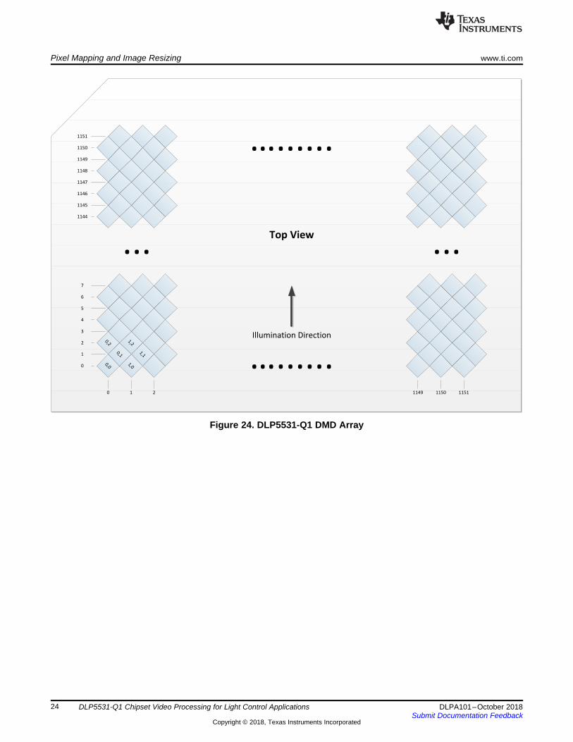
The DLP5531-Q1 has 1152 × 1152 diamond micromirror pixels as shown in Figure 24. Due to thediamond orientation, rows overlap by half a pixel while columns do not overlap. Therefore, the physicalaspect ratio of the DMD active mirror array is actually 2:1.
Pixel 0,0 is at the bottom left corner of the DMD. The DLPC230-Q1 supports digital flipping of the imageabout both axes to accommodate optical folds.
0,0
0,1
0,2
1,0
1,1
1,2
...
Y......
Y......
...
0 1 2 115111501149
1151
1150
1149
1148
1147
1146
1145
1144
7
6
5
4
3
2
1
0
Illumination Direction
Top View
Pixel Mapping and Image Resizing www.ti.com
24 DLPA101–October 2018Submit Documentation Feedback
Copyright © 2018, Texas Instruments Incorporated
DLP5531-Q1 Chipset Video Processing for Light Control Applications
Figure 24. DLP5531-Q1 DMD Array

...
Y......
Y......
...
0 1 2 115111501149
Illumination Direction
Top View
www.ti.com Pixel Mapping and Image Resizing
25DLPA101–October 2018Submit Documentation Feedback
Copyright © 2018, Texas Instruments Incorporated
DLP5531-Q1 Chipset Video Processing for Light Control Applications
Figure 25 highlights alternating columns (top-down).
Figure 25. DLP5531-Q1 DMD Array Columns

Graphics
ProcessorDLPC230-Q1
DLP553X-Q1 DMD
1152 x 576
2:1 Orthogonal
1152 x 1152
1:1 Orthogonal
1152 x 1152
2:1 Diamond
...
Y......
Y......
...
1151
1150
1149
1148
1147
1146
1145
1144
7
6
5
4
3
2
1
0
Illumination Direction
Top View
Pixel Mapping and Image Resizing www.ti.com
26 DLPA101–October 2018Submit Documentation Feedback
Copyright © 2018, Texas Instruments Incorporated
DLP5531-Q1 Chipset Video Processing for Light Control Applications
Figure 26 highlights alternating rows (left-right).
Figure 26. DLP5531-Q1 DMD Array Rows
The most commonly used input resolutions have a 2:1 aspect ratio, such as 1152 × 576. The DLPC230-Q1 will then perform scaling to address 1152 × 1152 pixels, and the physical geometry of the diamondDMD pixels will then display the output with the original 2:1 aspect ratio. Figure 27 shows an example ofthis process.
Figure 27. Scaling 2:1 Video Input

1,70,7
0,4
0,5
0,6
0,7
1,4
1,5
1,6
1,7
2,4
2,5
2,6
2,7
3,72,7
3,4
3,5
3,6
3,7 1,60,6 3,62,6
1,50,5 3,52,5
1,40,4 3,42,4
Diamond Pixel Array
(DLP553X-Q1) Orthogonal Pixel Array
5,74,7 7,76,7
5,64,6 7,66,6
5,54,5 7,56,5
5,44,4 7,46,4
1,30,3 3,32,3
1,20,2 3,22,2
1,10,1 3,12,1
1,00,0 3,02,0
5,34,3 7,36,3
5,24,2 7,26,2
5,14,1 7,16,1
5,04,0 7,06,0
0,0
0,1
0,2
0,3
1,0
1,1
1,2
1,3
2,0
2,1
2,2
2,3
3,0
3,1
3,2
3,3
4,4
4,5
4,6
4,7
5,4
5,5
5,6
5,7
6,4
6,5
6,6
6,7
7,4
7,5
7,6
7,7
4,0
4,1
4,2
4,3
5,0
5,1
5,2
5,3
6,0
6,1
6,2
6,3
7,0
7,1
7,2
7,3
www.ti.com Pixel Mapping and Image Resizing
27DLPA101–October 2018Submit Documentation Feedback
Copyright © 2018, Texas Instruments Incorporated
DLP5531-Q1 Chipset Video Processing for Light Control Applications
The benefit of providing a 2:1 aspect ratio resolution is that the graphics processor does not need toconsider aspect ratio distortion. The scaling process is handled by the DLP5531-Q1 chipset.
For most content, the diamond pixel array will not impact the display of the original image. Content thatspans multiple pixels will be displayed as desired because the diamond edges are not perceivable. Iffeatures within the video must be accurate on a pixel-level, then the native resolution of 1152 × 1152 mustbe input to the DLPC230-Q1 so that scaling is not used and each input pixel directly maps to an outputDMD mirror. An example of mapping a 1-pixel width diagonal line from diamond to orthogonal pixels isshown in Figure 28. The orthogonal array represents the video content that would need to be input to theDLPC230-Q1 at 1152 × 1152 resolution in order to display these diagonal lines on the DMD.
Figure 28. Diamond Pixel Diagonal Lines 1 Pixel
As features become larger, such as wider diagonal lines, they will appear more similar on both arrays.This is demonstrated with a 4-pixel width diagonal line in Figure 29. The orthogonal array displays asimilar diagonal line, but with 2x vertical scaling. This example with larger features is more typical of howcontent will appear.
Figure 29. Diamond Pixel Diagonal Lines 4 Pixels

Pixel Mapping and Image Resizing www.ti.com
28 DLPA101–October 2018Submit Documentation Feedback
Copyright © 2018, Texas Instruments Incorporated
DLP5531-Q1 Chipset Video Processing for Light Control Applications
6.2 Resolution SupportThe DLPC230-Q1 includes both image scaling and line replication to support a range of input resolutionsand size them to the full DMD area. Image scaling uses polyphase filtering, and is the preferred method ofresizing because it can reduce aliasing. Replication is only used for low input resolutions when the scalinglimit is reached. This directly replicates each row of pixels as they are output to the DMD.
All supported input resolutions are specified in the DLPC230-Q1 data sheet. Table 4 shows examples ofhow several image resolutions are resized. Note that the output resolution in all cases is the full DMDarray resolution in order to maximize light output.
Table 4. Resolution Resizing Examples
Input Resolution Output Resolution Horizontal Scaling Vertical Scaling Vertical Replication1152 × 1152 1152 × 1152 1x 1x 1x1152 × 576 1152 × 1152 1x 2x 1x576 × 288 1152 × 1152 2x 2x 2x
1152 × 576 and 576 × 288 input will appear on the DMD at the correct 2:1 aspect ratio because of thediamond pixel array, as described in Figure 27.
1152 × 1152 input will appear to be scaled vertically by 0.5x on the DMD, meaning the aspect ratio willchange from 1:1 input to 2:1 output. Video content may need to be scaled accordingly. Because of thisaspect ratio adjustment, this resolution is only recommended if higher resolution is necessary or if directpixel mapping is necessary.

IMPORTANT NOTICE AND DISCLAIMER
TI PROVIDES TECHNICAL AND RELIABILITY DATA (INCLUDING DATASHEETS), DESIGN RESOURCES (INCLUDING REFERENCEDESIGNS), APPLICATION OR OTHER DESIGN ADVICE, WEB TOOLS, SAFETY INFORMATION, AND OTHER RESOURCES “AS IS”AND WITH ALL FAULTS, AND DISCLAIMS ALL WARRANTIES, EXPRESS AND IMPLIED, INCLUDING WITHOUT LIMITATION ANYIMPLIED WARRANTIES OF MERCHANTABILITY, FITNESS FOR A PARTICULAR PURPOSE OR NON-INFRINGEMENT OF THIRDPARTY INTELLECTUAL PROPERTY RIGHTS.These resources are intended for skilled developers designing with TI products. You are solely responsible for (1) selecting the appropriateTI products for your application, (2) designing, validating and testing your application, and (3) ensuring your application meets applicablestandards, and any other safety, security, or other requirements. These resources are subject to change without notice. TI grants youpermission to use these resources only for development of an application that uses the TI products described in the resource. Otherreproduction and display of these resources is prohibited. No license is granted to any other TI intellectual property right or to any thirdparty intellectual property right. TI disclaims responsibility for, and you will fully indemnify TI and its representatives against, any claims,damages, costs, losses, and liabilities arising out of your use of these resources.TI’s products are provided subject to TI’s Terms of Sale (www.ti.com/legal/termsofsale.html) or other applicable terms available either onti.com or provided in conjunction with such TI products. TI’s provision of these resources does not expand or otherwise alter TI’s applicablewarranties or warranty disclaimers for TI products.
Mailing Address: Texas Instruments, Post Office Box 655303, Dallas, Texas 75265Copyright © 2018, Texas Instruments Incorporated