Diversity Processing WCDMA Cell Searcher … · Abstract- In this paper algorithmic and...
5
Abstract- In this paper algorithmic and implementation innovations for a novel diversity processing based WCDMA synchronization system are presented. The system employs a dual antenna front end system and a three stage pipelined synchronization technique to achieve slot, frame and code synchronization. The slot boundary section employs a hybrid matched filter/correlator approach for maximum flexibility and to minimize power consumption. The secondary stage section employs a novel maximum likelihood algorithm to perform frame boundary identification, while the third and final stage shares the RAKE engine correlators to perform code identification. The system was implemented in a 0.18 µm CMOS process with 1 poly and 6 metal layers. The total standard cell count is 28k implemented in 1mm 2 . The average power consumed over a full frame is 2 mW from a 1.8 V supply. I. INTRODUCTION With the advent of third generation (3G) cellular systems, data rates that users expect and the associated Quality of Service (QoS) requirements demanded by network providers have soared in comparison to second generation (2G) systems. Furthermore, the fact that these systems have to meet a tight power budget, fit within the size constraints of the next generation handsets as well as meet the cost constraints of a terminal device, have provided additional challenges. One technique that has shown tremendous potential in solving the dilemma of providing high data rates while causing a minimal overhead in complexity is spatial diversity. The feasibility of such an approach has been made possible due to advances in RF circuit techniques and integration [1]. Diversity processing directly translates to increased capacity and better coverage as well as less waiting time during the initial synchronization phase. This paper presents the synchronization section of a dual antenna receiver designed for 3G WCDMA. Figure 1 illustrates the improvement in the average waiting time using a dual antenna structure versus a single antenna solution. The average waiting time is defined as the time elapsed starting at the origination of a cell search for the transmitting base station until a successful lock is declared. The paper is organized as follows; section II describes diversity processing and its impact on synchronization access time. Sections III, IV, V discuss the primary, secondary, and final synchronization stages, respectively. Section VI presents the ASIC implementation of the system. The paper is concluded in Section VII. II. DIVERSITY PROCESSING Using dual antennas at the mobile station presents the demodulation core with extra “copies” of the signal that have statistically semi-independent noise. By combining these signals in a maximal ratio combining scheme the signal to noise ratio (SNR) can be significantly improved. This improvement can be demonstrated at all stages of the demodulation algorithm starting with the synchronization stages and ending at the final demodulation stage. Cell search in W-CDMA is performed using three channels, namely the Primary Synchronization Channel (P-SCH), the Secondary Synchronization Channel (S-SCH), and the Common Pilot Channel (CPICH) [2]. Figure 2 depicts the slot and frame formats of these channels. Each frame of 38400 chips (10 ms) is divided into 15 slots, of 2560 chips (0.67 ms). The CPICH is scrambled by the primary downlink scrambling code of the cell. There are 10 pilot symbols within each time slot, each spread by 256 chips. Unlike CPICH, the P-SCH and S-SCH are not scrambled by the primary downlink scrambling code [3]. As shown in Figure 2, the P-SCH sequence is transmitted once in every slot, and thus can be used for detecting the slot boundary. All cells use the same P-SCH sequence, and only one P-SCH matched filter is needed to detect the slot boundaries. This code structure leads to a three stage pipelined approach where the primary synchronization stage performs a correlation off the P-SCH and results in the identification of the correct slot boundary. Following the primary stage, the second stage obtains the frame boundary along with the code group number. Each code group specifies a set of 8 possible primary scrambling codes. Finally the third and final stage of synchronization is performed using the RAKE correlator banks and is used to decide on the exact code being used within the code group chosen by the second stage sync. This procedure is depicted in Figure 3. Figure 1. Average waiting time for single and dual antenna Diversity Processing WCDMA Cell Searcher Implementation Ahmed M. Eltawil 1 , Eugene Grayver 2 , Alireza Tarighat 1 , Jean Francois Frigon 1 , Kambiz Shoarinejad 1 , Hanli Zou 3 and Danijela Cabric 4 1 University of California, Los Angeles, 2 Aerospace Corporation, Elsegundo, California, 3 Broadcomm Corporation, Irvine, California, 4 University of California, Berkeley [email protected] 3900 0-7803-8521-7/04/$20.00 © 2004 IEEE
Transcript of Diversity Processing WCDMA Cell Searcher … · Abstract- In this paper algorithmic and...

Abstract- In this paper algorithmic and implementation innovations for a novel diversity processing based WCDMA synchronization system are presented. The system employs a dual antenna front end system and a three stage pipelined synchronization technique to achieve slot, frame and code synchronization. The slot boundary section employs a hybrid matched filter/correlator approach for maximum flexibility and to minimize power consumption. The secondary stage section employs a novel maximum likelihood algorithm to perform frame boundary identification, while the third and final stage shares the RAKE engine correlators to perform code identification. The system was implemented in a 0.18 µm CMOS process with 1 poly and 6 metal layers. The total standard cell count is 28k implemented in 1mm2. The average power consumed over a full frame is 2 mW from a 1.8 V supply.
I. INTRODUCTION With the advent of third generation (3G) cellular systems, data rates that users expect and the associated Quality of Service (QoS) requirements demanded by network providers have soared in comparison to second generation (2G) systems. Furthermore, the fact that these systems have to meet a tight power budget, fit within the size constraints of the next generation handsets as well as meet the cost constraints of a terminal device, have provided additional challenges. One technique that has shown tremendous potential in solving the dilemma of providing high data rates while causing a minimal overhead in complexity is spatial diversity. The feasibility of such an approach has been made possible due to advances in RF circuit techniques and integration [1]. Diversity processing directly translates to increased capacity and better coverage as well as less waiting time during the initial synchronization phase. This paper presents the synchronization section of a dual antenna receiver designed for 3G WCDMA. Figure 1 illustrates the improvement in the average waiting time using a dual antenna structure versus a single antenna solution. The average waiting time is defined as the time elapsed starting at the origination of a cell search for the transmitting base station until a successful lock is declared. The paper is organized as follows; section II describes diversity processing and its impact on synchronization access time. Sections III, IV, V discuss the primary, secondary, and final synchronization stages, respectively. Section VI presents the ASIC implementation of the system. The paper is concluded in Section VII.
II. DIVERSITY PROCESSING Using dual antennas at the mobile station presents the demodulation core with extra “copies” of the signal that have statistically semi-independent noise. By combining
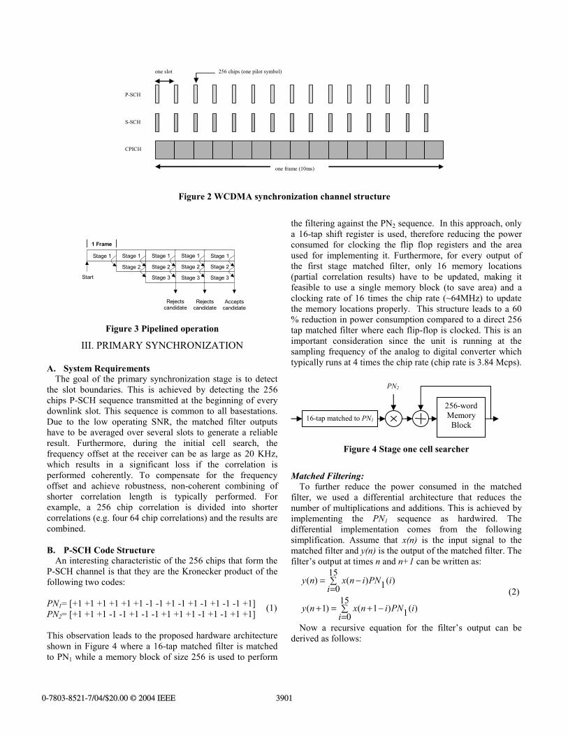
these signals in a maximal ratio combining scheme the signal to noise ratio (SNR) can be significantly improved. This improvement can be demonstrated at all stages of the demodulation algorithm starting with the synchronization stages and ending at the final demodulation stage. Cell search in W-CDMA is performed using three channels, namely the Primary Synchronization Channel (P-SCH), the Secondary Synchronization Channel (S-SCH), and the Common Pilot Channel (CPICH) [2]. Figure 2 depicts the slot and frame formats of these channels. Each frame of 38400 chips (10 ms) is divided into 15 slots, of 2560 chips (0.67 ms). The CPICH is scrambled by the primary downlink scrambling code of the cell. There are 10 pilot symbols within each time slot, each spread by 256 chips. Unlike CPICH, the P-SCH and S-SCH are not scrambled by the primary downlink scrambling code [3]. As shown in Figure 2, the P-SCH sequence is transmitted once in every slot, and thus can be used for detecting the slot boundary. All cells use the same P-SCH sequence, and only one P-SCH matched filter is needed to detect the slot boundaries. This code structure leads to a three stage pipelined approach where the primary synchronization stage performs a correlation off the P-SCH and results in the identification of the correct slot boundary. Following the primary stage, the second stage obtains the frame boundary along with the code group number. Each code group specifies a set of 8 possible primary scrambling codes. Finally the third and final stage of synchronization is performed using the RAKE correlator banks and is used to decide on the exact code being used within the code group chosen by the second stage sync. This procedure is depicted in Figure 3.
Figure 1. Average waiting time for single and dual antenna
Diversity Processing WCDMA Cell Searcher Implementation Ahmed M. Eltawil1, Eugene Grayver2, Alireza Tarighat1, Jean Francois Frigon1, Kambiz Shoarinejad1, Hanli Zou3 and
Danijela Cabric4 1University of California, Los Angeles, 2Aerospace Corporation, Elsegundo, California, 3Broadcomm Corporation, Irvine,
California, 4University of California, Berkeley [email protected]
0-7803-8521-7/04/$20.00 (C) 2004 IEEE
39000-7803-8521-7/04/$20.00 © 2004 IEEE
P-SCH
S-SCH
CPICH
one frame (10ms)
one slot 256 chips (one pilot symbol)
Figure 2 WCDMA synchronization channel structure
1 Frame
Stage 1
Stage 2
Stage 3
Stage 1
Stage 2
Stage 3
Stage 1
Stage 2
Stage 3
Stage 1
Stage 2
Stage 1
Rejects candidate
Rejects candidate
Accepts candidate
Start
Figure 3 Pipelined operation
III. PRIMARY SYNCHRONIZATION
A. System Requirements The goal of the primary synchronization stage is to detect the slot boundaries. This is achieved by detecting the 256 chips P-SCH sequence transmitted at the beginning of every downlink slot. This sequence is common to all basestations. Due to the low operating SNR, the matched filter outputs have to be averaged over several slots to generate a reliable result. Furthermore, during the initial cell search, the frequency offset at the receiver can be as large as 20 KHz, which results in a significant loss if the correlation is performed coherently. To compensate for the frequency offset and achieve robustness, non-coherent combining of shorter correlation length is typically performed. For example, a 256 chip correlation is divided into shorter correlations (e.g. four 64 chip correlations) and the results are combined. B. P-SCH Code Structure An interesting characteristic of the 256 chips that form the P-SCH channel is that they are the Kronecker product of the following two codes: PN1= [+1 +1 +1 +1 +1 +1 -1 -1 +1 -1 +1 -1 +1 -1 -1 +1] PN2= [+1 +1 +1 -1 -1 +1 -1 -1 +1 +1 +1 -1 +1 -1 +1 +1] This observation leads to the proposed hardware architecture shown in Figure 4 where a 16-tap matched filter is matched to PN1 while a memory block of size 256 is used to perform
the filtering against the PN2 sequence. In this approach, only a 16-tap shift register is used, therefore reducing the power consumed for clocking the flip flop registers and the area used for implementing it. Furthermore, for every output of the first stage matched filter, only 16 memory locations (partial correlation results) have to be updated, making it feasible to use a single memory block (to save area) and a clocking rate of 16 times the chip rate (~64MHz) to update the memory locations properly. This structure leads to a 60 % reduction in power consumption compared to a direct 256 tap matched filter where each flip-flop is clocked. This is an important consideration since the unit is running at the sampling frequency of the analog to digital converter which typically runs at 4 times the chip rate (chip rate is 3.84 Mcps).
Figure 4 Stage one cell searcher
Matched Filtering: To further reduce the power consumed in the matched filter, we used a differential architecture that reduces the number of multiplications and additions. This is achieved by implementing the PN1 sequence as hardwired. The differential implementation comes from the following simplification. Assume that x(n) is the input signal to the matched filter and y(n) is the output of the matched filter. The filter’s output at times n and n+1 can be written as:
∑=
−=15
0)(1)()(
iiPNinxny
∑=
−+=+15
0)(1)1()1(
iiPNinxny
Now a recursive equation for the filter’s output can be derived as follows:
16-tap matched to PN1 256-wordMemory
Block
PN2
(2)
(1)
0-7803-8521-7/04/$20.00 (C) 2004 IEEE
39010-7803-8521-7/04/$20.00 © 2004 IEEE

)]15(10)[15()]14(1)15(1)[14(
)]0(1)1(1)[(]0)0(1)[1()()1(
PNnxPNPNnx
PNPNnxPNnxnyny
−−+−−+
+−+−++=+
The matched filter output can be derived recursively from the previous computed output by performing the correlation against a new sequence defined as: ]10[]01[ PNPNdiffPN −=
This new sequence basically contains the difference between all consecutive elements of the original PN1 sequence. About half of the elements in the new sequence are zero, therefore reducing the number of multiplications-additions in implementing the original matched filter. Correlation Bank: The main motivation to have a correlation bank using a memory block instead of regular matched filter is its area efficient architecture, and the fact that the memory block can be used to temporarily store the partial results of the correlation results. The RAM or Register File (RF) implementation of memory locations is much more area efficient than regular flip-flop based storage. This is the case since the number of memory locations for primary and secondary synchronization is relatively large (256-500 words of 12 to 24 bits). The other advantage of the two-stage matched filter/correlation bank is its lower clocking rate (by a factor of 16) compared to other alternatives. Only 16 memory locations in the two-stage architecture are updated (clocked) for every received chip sample. Diversity Combining To benefit from diversity a non-coherent sum of contributions from both antennas is performed and the results are transferred to a supervising micro-controller that decides on valid peaks. Figure 5 illustrates the probability of error in detection (Pe) of a dual antenna system versus a single antenna system for different Doppler frequencies in a flat fading environment.
Figure 5 Performance in a flat fading channel
IV. SECOND STAGE SYNCHRONIZATION Following the primary synchronization, the slot boundary is identified, the second stage utilizes this information to lock
onto the frame boundary as well as identify the code group used. This is achieved by using two synchronization channels, namely the P-SCH and the S-SCH. As shown in Figure 1 the S-SCH consists of a symbol that is transmitted in the first 256 chips of the slot. There are 15 different slots in a frame. The structure of the Secondary Synchronization Channel (S-SCH) is as follows:
ci,0 ci,1
256chips
2560 chips
Slot #0 Slot #1
ci,14
Slot #14
10 ms SCH radio frame
S-SCH
• The above sequence gets repeated in every frame
• There are a total of 64 possible sequences
• Each kiC , is a 256 chips sequence, taken from a 16-ary codebook. The specific structure of the codewords is given in [2].
The codewords kiC , are assigned for different slots (slot #0 to slot #14) for different code groups (group #0 to group #63) based on a Reed-Solomon (RS) code. The structure of the codebook is such that a non-zero cyclic shift less than 15 of any of the 64 code sequences is never equivalent to some cyclic shift of any other of the 64 sequences, or the cyclic shift of the codeword itself. In the second stage synchronization, one should recover from the received samples on S-SCH, which code sequence has been sent and what the corresponding offset is, i.e., the frame start. This information will be passed onto the third stage synchronization to obtain the exact scrambling code from the common pilot channel (CPICH). The implementation of the second stage synchronization can be considered in two steps: 1- Computation of the required correlation values 2- RS Decoding, i.e. finding the code sequence (group
number) and the corresponding offset (frame boundary). There are multiple implementations that could be considered for the second stage. 1- A straight forward approach would be to perform
decoding on a symbol by symbol basis followed by a hard decision on that symbol. At the end of the frame 15 decisions are available and a code group selection could be performed. This approach is very simple to implement but results in extremely poor performance due to the hard decision.
2- A second approach is to perform maximum likelihood decision. In this case a correlation is performed on a symbol by symbol basis however for each slot. Using 16 correlation values per slot a table is constructed consisting of a (64 code_sequence x 15 offset) matrix by inserting the value of the correlation with the codeword
(3)
(4)
0-7803-8521-7/04/$20.00 (C) 2004 IEEE
39020-7803-8521-7/04/$20.00 © 2004 IEEE

number K in every (i,j) location of the matrix if KCind ji =)( , . (i=0,…,63 and j=0,…,14). At the end
of the frame the row and column that have the maximum value is the required candidate. The total number of computations is: (16 correlations + 64 x 15 additions)/slot x 15 slots. While there are a total number of 960 x 15 additions, the advantage of this scheme is that these additions are distributed in the whole frame. The major disadvantage, however, is the memory requirement, since a 64 x 15 matrix should be saved and therefore 960 memory words are required.
3- The final and novel approach to this problem results in a compact highly efficient architecture by rearranging the maximum likelihood calculation. A correlation is performed on a symbol by symbol basis against all possible 16 values. Thus on a slot by slot basis 16 correlations values are computed. This is repeated for each slot to generate a 15x16 matrix as follows
14,161,160,16
14,21,20,2
14,11,10,1
SSS
SSSSSS
where jiS , is the value of the correlation between the received samples on the j-th slot (j=0,…,14) and the codeword with index i (i=1,…,16). The idea is to obtain the correlations with all possible sequences over a frame with all possible offsets and pick the maximum correlation. Using the codebook table, the correlation corresponding to group number i (i=0,…,63) and offset j (j=0,…,14) is obtained as:
∑=
+=14
0,)( 15mod)(,),(
mmCind mjiSjiCorr
Recall that )( 15mod)(, mjiCind + is taken from the codebook table and is a number from 1 to 16. This scheme obtains the same metrics as scheme II, and therefore finds the ML solution and performs better than a hard-decision scheme. The number of computations: 16 correlations/slot x 15 slots + 960 x 15 additions The major advantage of this scheme over Scheme II is that only 16 x 15 = 240 memory words are required. Note that there is no need to keep all ),( jiCorr ’s anymore, as we are only interested in the maximum value. In other words, every calculated ),( jiCorr is compared against the previous one and the bigger one is picked. Moreover, the same number of additions (960 x 15) is required in Scheme III as in Scheme II. Correlator Circuit Design When designing the S-SCH correlation block three main points were considered.
• A relatively high frequency offset of +/- 20 KHz might still affect the data since fine frequency acquisition has not yet been initiated.
• The dual antenna structure must be utilized to improve performance.
• An inverse Hadamard transformation should be used to implement the final RS decoding due to its hardware efficient fast implementation similar to the FFT.
To address these points, the correlator was split into two parallel channels, one correlating off the P-SCH channel while the second correlates of the S-SCH. Since the P-SCH is always transmitted simultaneously to the S-SCH, the P-SCH can be used as a phase reference for the S-SCH. A non-coherent processing is used where the inputs to the inverse Hadamard transform are corrected by a channel estimate computed using 64 chips from the P-SCH. The inputs from both antennas are then combined together using the channel estimate in a manner similar to maximal ratio combining. That is, for slot j, the 16 inputs to the inverse Hadamard transform are given by:
14,,0,15,,0Real2
1
34
4
44
,,,,,
*
…… ==
= ∑ ∑
=
+
=
jiyysn
i
ik
pnkj
snijij
Where i is the symbol index, n is the antenna index, yp is the correlation result from the P-SCH channel and ys is the correlation result for the S-SCH channel. Figure 7 illustrates the final block design. Figure 6 illustrates the impact of MRC on the probability of error in detection (Pe). One sample per chip was used to calculate correlation values. Three cases are considered. Offset 1 corresponds to the optimum sampling point. Offset 2 is the sample next to the optimum sampling point with 4 times oversampling ratio, while offset 3 is the sample on the boundary between two consecutive chips. We can observe that in all cases MRC show an improvement in performance.
V. THIRD STAGE SYNCHRONIZATION
The second synchronization stage identified the frame timing and narrows down the set of possible PN codes to 8. The purpose of the third stage is to determine which of the 8 possible PN codes is being used. The output of this stage also provides a final confidence check of the overall synchronization. Eight correlators are used to check the 8 possible codes in parallel. Each correlator has an associated PN generator, programmed to generate one of the codes being tested. The correlators process the common pilot channel (CPICH) and accumulate the magnitudes of N-chip correlations over the duration of a frame. Just like the previous two stages, the third stage must operate with a frequency offset of up to 20kHz. Fortunately, the correlators are highly programmable and N can be set to any value. The outputs for each correlator are then accumulated non-coherently L times. A majority voting scheme is implemented after every L*N chips. The
(5)
(6)
(7)
0-7803-8521-7/04/$20.00 (C) 2004 IEEE
39030-7803-8521-7/04/$20.00 © 2004 IEEE

counter corresponding to the correlator with the largest accumulated value is incremented. This procedure is repeated for the duration of a frame and results in P=38400/(L*N) votes. After a frame is complete, the resultant 8-element vector is passed to the uP. The index of the largest value in the vector identifies the most likely PN code, while the relative magnitudes of the values indicate the confidence in the result. This configuration is shown in Figure 8.
Figure 6 MRC impact on probability of error
8x
8x
Dual AntennaSSC Correlator
Accumulateover 15 slotsand selectmaximumlikelihood
Candidate CodeGroup and Frame
Boundary
rk,1
rk,2
ysj,i,1
1x
1x
Dual AntennaPSC Correlator
Initial CellSearch Inverse
HadamardTransform
ypj,i,1
hj,1
hj,16
AdjustedSampling Offset
from Stage 1
Slot Offsetfrom Stage 1
ysj,i,2
ypj,i,2
PN-PSC
PN-SSC
Figure 7 Dual Antenna Secondary Synchronization
Stucture
VI. ASIC Implementation To verify the functionality of the design an ASIC incorporating the cell searcher described in this paper as well as a RAKE receiver core and front end digital signal processing (filtering, timing and frequency synchronization) was implemented in a 0.18 µm CMOS technology. The total area of the chip is 4 mm2 with a total of 90 Kgates. The synchronization block takes up 1mm2 area and uses under 28k standard cells. The total power consumption of the chip with all resources running is 18 mw. The die photo of the fabricated ASIC showing the location of the cell searcher is shown in Figure 9.
Figure 8. Block diagram for the 3rd stage (times in chips)
Figure 9 RAKE receiver ASIC
VII. CONCLUSION A novel and robust diversity processing synchronization engine for 3G WCDMA has been presented. The architecture utilizes statistically independent multipath received from two antennas to accelerate the average cell search time and increase the probability of a successful search. System and circuit techniques were employed to minimize the complexity of the final system. The architecture has been successfully tested and proven on silicon in a 0.18 µm CMOS technology. The entire synchronization block takes up about 1mm2 area and uses under 28k standard cells. The peak power consumption with all three stages running was measured to be 20mW while the average over a full frame is 2mW.
REFERENCES [1] B. Razavi, “RF CMOS transceivers for cellular
telephony,” IEEE Communications Magazine, vol.41, no.8, pp.144-9, Aug. 2003.
[2] 3rd Generation Partnership Project, “Physical channels and mapping of transport channels onto physical channels (FDD),” 3GPP Tech. Spec., TS 25.211, V3.0.0, Oct. 1999.
[3] Siemens and Texas Instruments, “Generalized hierarchical Golay sequence for PSC with low complexity correlation using pruned efficient Golay correlators,” 3GPP Tech. Doc., Tech. Doc. R1-99554, Cheju, Korea, June 1999.
[4] Y. E. Wang and T. Ottosson, “Cell search in W-CDMA,” IEEE Journal on Selected Areas in Communications, vol. 18. No. 8, pp. 1470-1482, August 2000.
RA
M1
RA
M2 Primary Synch
Memories AB
R
AM
Searcher
0-7803-8521-7/04/$20.00 (C) 2004 IEEE
39040-7803-8521-7/04/$20.00 © 2004 IEEE