Distributed by: 1-800-831-4242 Jameco Part ... · ry (EEPROM) devices are accessed through a...
32
The content and copyrights of the attached material are the property of its owner. Distributed by: www.Jameco.com ✦ 1-800-831-4242
Transcript of Distributed by: 1-800-831-4242 Jameco Part ... · ry (EEPROM) devices are accessed through a...

The content and copyrights of the attached material are the property of its owner.
Distributed by:
www.Jameco.com 1-800-831-4242
JMendiola
Text Box
Jameco Part Number 1393643
1/31October 2005
M93C86, M93C76, M93C66M93C56, M93C46
16Kbit, 8Kbit, 4Kbit, 2Kbit and 1Kbit (8-bit or 16-bit wide)MICROWIRE® Serial Access EEPROM
FEATURES SUMMARY Industry Standard MICROWIRE Bus Single Supply Voltage:
– 4.5 to 5.5V for M93Cx6– 2.5 to 5.5V for M93Cx6-W– 1.8 to 5.5V for M93Cx6-R
Dual Organization: by Word (x16) or Byte (x8) Programming Instructions that work on: Byte,
Word or Entire Memory Self-timed Programming Cycle with Auto-
Erase: 5ms Ready/Busy Signal During Programming 2MHz Clock Rate Sequential Read Operation Enhanced ESD/Latch-Up Behavior More than 1 Million Erase/Write Cycles More than 40 Year Data Retention Packages
– ECOPACK® (RoHS compliant)
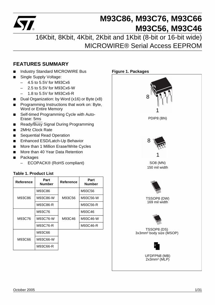
Table 1. Product List
Figure 1. Packages
Reference Part Number Reference Part
Number
M93C86
M93C86
M93C56
M93C56
M93C86-W M93C56-W
M93C86-R M93C56-R
M93C76
M93C76
M93C46
M93C46
M93C76-W M93C46-W
M93C76-R M93C46-R
M93C66
M93C66
M93C66-W
M93C66-R
PDIP8 (BN)
SO8 (MN)150 mil width
8
1
TSSOP8 (DW)169 mil width
TSSOP8 (DS)3x3mm² body size (MSOP)
8
1
UFDFPN8 (MB)2x3mm² (MLP)

M93C86, M93C76, M93C66, M93C56, M93C46
2/31
TABLE OF CONTENTS
FEATURES SUMMARY . . . . . . . . . . . . . . . . . . . . . . . . . . . . . . . . . . . . . . . . . . . . . . . . . . . . . . . . . . . . . 1
Table 1. Product List . . . . . . . . . . . . . . . . . . . . . . . . . . . . . . . . . . . . . . . . . . . . . . . . . . . . . . . . . . . . 1Figure 1. Packages . . . . . . . . . . . . . . . . . . . . . . . . . . . . . . . . . . . . . . . . . . . . . . . . . . . . . . . . . . . . . . 1Figure 2. Logic Diagram . . . . . . . . . . . . . . . . . . . . . . . . . . . . . . . . . . . . . . . . . . . . . . . . . . . . . . . . . . 4Table 2. Signal Names . . . . . . . . . . . . . . . . . . . . . . . . . . . . . . . . . . . . . . . . . . . . . . . . . . . . . . . . . . 4Table 3. Memory Size versus Organization. . . . . . . . . . . . . . . . . . . . . . . . . . . . . . . . . . . . . . . . . . . 4Table 4. Instruction Set for the M93Cx6 . . . . . . . . . . . . . . . . . . . . . . . . . . . . . . . . . . . . . . . . . . . . . 4Figure 3. DIP, SO, TSSOP and MLP Connections (Top View). . . . . . . . . . . . . . . . . . . . . . . . . . . . . 5
MEMORY ORGANIZATION . . . . . . . . . . . . . . . . . . . . . . . . . . . . . . . . . . . . . . . . . . . . . . . . . . . . . . . . . . 6
INTERNAL DEVICE RESET . . . . . . . . . . . . . . . . . . . . . . . . . . . . . . . . . . . . . . . . . . . . . . . . . . . . . . . . . . 6
ACTIVE POWER AND STANDBY POWER MODES . . . . . . . . . . . . . . . . . . . . . . . . . . . . . . . . . . . . . . . 6
INSTRUCTIONS . . . . . . . . . . . . . . . . . . . . . . . . . . . . . . . . . . . . . . . . . . . . . . . . . . . . . . . . . . . . . . . . . . . 7
Table 5. Instruction Set for the M93C46 . . . . . . . . . . . . . . . . . . . . . . . . . . . . . . . . . . . . . . . . . . . . . 7Table 6. Instruction Set for the M93C56 and M93C66 . . . . . . . . . . . . . . . . . . . . . . . . . . . . . . . . . . 8Table 7. Instruction Set for the M93C76 and M93C86 . . . . . . . . . . . . . . . . . . . . . . . . . . . . . . . . . . 8Read . . . . . . . . . . . . . . . . . . . . . . . . . . . . . . . . . . . . . . . . . . . . . . . . . . . . . . . . . . . . . . . . . . . . . . . . . 9Erase/Write Enable and Disable. . . . . . . . . . . . . . . . . . . . . . . . . . . . . . . . . . . . . . . . . . . . . . . . . . . 9Figure 4. READ, WRITE, EWEN, EWDS Sequences. . . . . . . . . . . . . . . . . . . . . . . . . . . . . . . . . . . . 9Erase. . . . . . . . . . . . . . . . . . . . . . . . . . . . . . . . . . . . . . . . . . . . . . . . . . . . . . . . . . . . . . . . . . . . . . . . 10Write . . . . . . . . . . . . . . . . . . . . . . . . . . . . . . . . . . . . . . . . . . . . . . . . . . . . . . . . . . . . . . . . . . . . . . . . 10Figure 5. ERASE, ERAL Sequences . . . . . . . . . . . . . . . . . . . . . . . . . . . . . . . . . . . . . . . . . . . . . . . 10Erase All . . . . . . . . . . . . . . . . . . . . . . . . . . . . . . . . . . . . . . . . . . . . . . . . . . . . . . . . . . . . . . . . . . . . . 11Write All . . . . . . . . . . . . . . . . . . . . . . . . . . . . . . . . . . . . . . . . . . . . . . . . . . . . . . . . . . . . . . . . . . . . . 11Figure 6. WRAL Sequence . . . . . . . . . . . . . . . . . . . . . . . . . . . . . . . . . . . . . . . . . . . . . . . . . . . . . . . 11
READY/BUSY STATUS . . . . . . . . . . . . . . . . . . . . . . . . . . . . . . . . . . . . . . . . . . . . . . . . . . . . . . . . . . . . 12
INITIAL DELIVERY STATE. . . . . . . . . . . . . . . . . . . . . . . . . . . . . . . . . . . . . . . . . . . . . . . . . . . . . . . . . . 12
COMMON I/O OPERATION . . . . . . . . . . . . . . . . . . . . . . . . . . . . . . . . . . . . . . . . . . . . . . . . . . . . . . . . . 12
CLOCK PULSE COUNTER . . . . . . . . . . . . . . . . . . . . . . . . . . . . . . . . . . . . . . . . . . . . . . . . . . . . . . . . . 12
Figure 7. Write Sequence with One Clock Glitch . . . . . . . . . . . . . . . . . . . . . . . . . . . . . . . . . . . . . . 12
MAXIMUM RATING. . . . . . . . . . . . . . . . . . . . . . . . . . . . . . . . . . . . . . . . . . . . . . . . . . . . . . . . . . . . . . . . 13
Table 8. Absolute Maximum Ratings . . . . . . . . . . . . . . . . . . . . . . . . . . . . . . . . . . . . . . . . . . . . . . . 13
DC AND AC PARAMETERS. . . . . . . . . . . . . . . . . . . . . . . . . . . . . . . . . . . . . . . . . . . . . . . . . . . . . . . . . 14
Table 9. Operating Conditions (M93Cx6) . . . . . . . . . . . . . . . . . . . . . . . . . . . . . . . . . . . . . . . . . . . 14Table 10. Operating Conditions (M93Cx6-W) . . . . . . . . . . . . . . . . . . . . . . . . . . . . . . . . . . . . . . . . . 14Table 11. Operating Conditions (M93Cx6-R) . . . . . . . . . . . . . . . . . . . . . . . . . . . . . . . . . . . . . . . . . 14

3/31
M93C86, M93C76, M93C66, M93C56, M93C46
Table 12. AC Measurement Conditions (M93Cx6) . . . . . . . . . . . . . . . . . . . . . . . . . . . . . . . . . . . . . 15Table 13. AC Measurement Conditions (M93Cx6-W and M93Cx6-R) . . . . . . . . . . . . . . . . . . . . . . 15Figure 8. AC Testing Input Output Waveforms. . . . . . . . . . . . . . . . . . . . . . . . . . . . . . . . . . . . . . . . 15Table 14. Capacitance. . . . . . . . . . . . . . . . . . . . . . . . . . . . . . . . . . . . . . . . . . . . . . . . . . . . . . . . . . . 15Table 15. DC Characteristics (M93Cx6, Device Grade 6) . . . . . . . . . . . . . . . . . . . . . . . . . . . . . . . . 16Table 16. DC Characteristics (M93Cx6, Device Grade 7 or 3) . . . . . . . . . . . . . . . . . . . . . . . . . . . . 16Table 17. DC Characteristics (M93Cx6-W, Device Grade 6) . . . . . . . . . . . . . . . . . . . . . . . . . . . . . 17Table 18. DC Characteristics (M93Cx6-W, Device Grade 7 or 3) . . . . . . . . . . . . . . . . . . . . . . . . . . 18Table 19. DC Characteristics (M93Cx6-R) . . . . . . . . . . . . . . . . . . . . . . . . . . . . . . . . . . . . . . . . . . . 18Table 20. AC Characteristics (M93Cx6, Device Grade 6, 7 or 3) . . . . . . . . . . . . . . . . . . . . . . . . . . 19Table 21. AC Characteristics (M93Cx6-W, Device Grade 6). . . . . . . . . . . . . . . . . . . . . . . . . . . . . . 20Table 22. AC Characteristics (M93Cx6-W, Device Grade 7 or 3) . . . . . . . . . . . . . . . . . . . . . . . . . . 21Table 23. AC Characteristics (M93Cx6-R) . . . . . . . . . . . . . . . . . . . . . . . . . . . . . . . . . . . . . . . . . . . 22Figure 9. Synchronous Timing (Start and Op-Code Input) . . . . . . . . . . . . . . . . . . . . . . . . . . . . . . . 23Figure 10.Synchronous Timing (Read or Write) . . . . . . . . . . . . . . . . . . . . . . . . . . . . . . . . . . . . . . . 23Figure 11.Synchronous Timing (Read or Write) . . . . . . . . . . . . . . . . . . . . . . . . . . . . . . . . . . . . . . . 23
PACKAGE MECHANICAL . . . . . . . . . . . . . . . . . . . . . . . . . . . . . . . . . . . . . . . . . . . . . . . . . . . . . . . . . . 24
Figure 12.PDIP8 – 8 pin Plastic DIP, 0.25mm lead frame, Package Outline . . . . . . . . . . . . . . . . . 24Table 24. PDIP8 – 8 pin Plastic DIP, 0.25mm lead frame, Package Mechanical Data . . . . . . . . . . 24Figure 13.SO8 narrow – 8 lead Plastic Small Outline, 150 mils body width, Package Outline . . . . 25Table 25. SO8 narrow – 8 lead Plastic Small Outline, 150 mils body width, Package Data . . . . . . 25Figure 14.UFDFPN8 (MLP8) 8-lead Ultra thin Fine pitch Dual Flat Package No lead 2x3mm²,
Outline . . . . . . . . . . . . . . . . . . . . . . . . . . . . . . . . . . . . . . . . . . . . . . . . . . . . . . . . . . . . . . . 26Table 26. UFDFPN8 (MLP8) 8-lead Ultra thin Fine pitch Dual Flat Package No lead 2x3mm²,
Data . . . . . . . . . . . . . . . . . . . . . . . . . . . . . . . . . . . . . . . . . . . . . . . . . . . . . . . . . . . . . . . . . 26Figure 15.TSSOP8 3x3mm² – 8 lead Thin Shrink Small Outline, 3x3mm² body size, Package
Outline . . . . . . . . . . . . . . . . . . . . . . . . . . . . . . . . . . . . . . . . . . . . . . . . . . . . . . . . . . . . . . . 27Table 27. TSSOP8 3x3mm² – 8 lead Thin Shrink Small Outline, 3x3mm² body size,
Mechanical Data . . . . . . . . . . . . . . . . . . . . . . . . . . . . . . . . . . . . . . . . . . . . . . . . . . . . . . . 27Figure 16.TSSOP8 – 8 lead Thin Shrink Small Outline, Package Outline . . . . . . . . . . . . . . . . . . . 28Table 28. TSSOP8 – 8 lead Thin Shrink Small Outline, Package Mechanical Data . . . . . . . . . . . . 28
PART NUMBERING . . . . . . . . . . . . . . . . . . . . . . . . . . . . . . . . . . . . . . . . . . . . . . . . . . . . . . . . . . . . . . . 29
Table 29. Ordering Information Scheme . . . . . . . . . . . . . . . . . . . . . . . . . . . . . . . . . . . . . . . . . . . . . 29
REVISION HISTORY. . . . . . . . . . . . . . . . . . . . . . . . . . . . . . . . . . . . . . . . . . . . . . . . . . . . . . . . . . . . . . . 31
Table 30. Document Revision History . . . . . . . . . . . . . . . . . . . . . . . . . . . . . . . . . . . . . . . . . . . . . . . 31

M93C86, M93C76, M93C66, M93C56, M93C46
4/31
SUMMARY DESCRIPTIONThese electrically erasable programmable memo-ry (EEPROM) devices are accessed through a Se-rial Data Input (D) and Serial Data Output (Q)using the MICROWIRE bus protocol.In order to meet environmental requirements, SToffers these devices in ECOPACK® packages.ECOPACK® packages are Lead-free and RoHScompliant.ECOPACK is an ST trademark. ECOPACK speci-fications are available at: www.st.com.
Figure 2. Logic Diagram
Table 2. Signal Names
The memory array organization may be dividedinto either bytes (x8) or words (x16) which may beselected by a signal applied on Organization Se-
lect (ORG). The bit, byte and word sizes of thememories are as shown in Table 3.
Table 3. Memory Size versus Organization
The M93Cx6 is accessed by a set of instructions,as summarized in Table 4., and in more detail inTable 5. to Table 7.).
Table 4. Instruction Set for the M93Cx6
A Read Data from Memory (READ) instructionloads the address of the first byte or word to beread in an internal address register. The data atthis address is then clocked out serially. The ad-dress register is automatically incremented afterthe data is output and, if Chip Select Input (S) isheld High, the M93Cx6 can output a sequentialstream of data bytes or words. In this way, thememory can be read as a data stream from eightto 16384 bits long (in the case of the M93C86), orcontinuously (the address counter automaticallyrolls over to 00h when the highest address isreached). Programming is internally self-timed (the externalclock signal on Serial Clock (C) may be stopped orleft running after the start of a Write cycle) anddoes not require an Erase cycle prior to the Writeinstruction. The Write instruction writes 8 or 16 bitsat a time into one of the byte or word locations ofthe M93Cx6. After the start of the programming cy-cle, a Busy/Ready signal is available on Serial
S Chip Select Input
D Serial Data Input
Q Serial Data Output
C Serial Clock
ORG Organisation Select
VCC Supply Voltage
VSS Ground
AI01928
D
VCC
M93Cx6
VSS
C
Q
S
ORG
Device Number of Bits
Number of 8-bit Bytes
Number of 16-bit Words
M93C86 16384 2048 1024
M93C76 8192 1024 512
M93C66 4096 512 256
M93C56 2048 256 128
M93C46 1024 128 64
Instruction Description Data
READ Read Data from Memory Byte or Word
WRITE Write Data to Memory Byte or Word
EWEN Erase/Write Enable
EWDS Erase/Write Disable
ERASE Erase Byte or Word Byte or Word
ERAL Erase All Memory
WRALWrite All Memorywith same Data

5/31
M93C86, M93C76, M93C66, M93C56, M93C46
Data Output (Q) when Chip Select Input (S) is driv-en High.An internal Power-on Data Protection mechanismin the M93Cx6 inhibits the device when the supplyis too low.
Figure 3. DIP, SO, TSSOP and MLP Connections (Top View)
Note: 1. See PACKAGE MECHANICAL section for package di-mensions, and how to identify pin-1.
2. DU = Don’t Use.
The DU (Don’t Use) pin does not contribute to thenormal operation of the device. It is reserved foruse by STMicroelectronics during test sequences.The pin may be left unconnected or may be con-nected to VCC or VSS. Direct connection of DU toVSS is recommended for the lowest stand-by pow-er consumption.
VSSQORGDUC
S VCC
D
AI01929B
M93Cx6
1234
8765
M93C86, M93C76, M93C66, M93C56, M93C46
6/31
MEMORY ORGANIZATIONThe M93Cx6 memory is organized either as bytes(x8) or as words (x16). If Organization Select(ORG) is left unconnected (or connected to VCC)the x16 organization is selected; when Organiza-tion Select (ORG) is connected to Ground (VSS)the x8 organization is selected. When the M93Cx6
is in stand-by mode, Organization Select (ORG)should be set either to VSS or VCC for minimumpower consumption. Any voltage between VSSand VCC applied to Organization Select (ORG)may increase the stand-by current.
INTERNAL DEVICE RESETIn order to prevent inadvertent Write operationsduring Power-up, a Power On Reset (POR) circuitis included.At Power-up and Power-down, the device mustnot be selected (that is, the Chip Select Input (S)must be driven Low) until the supply voltagereaches the operating voltage VCC (as defined inTables 9, 10 and 11).During Power-up (phase during which VCC is low-er than VCCmin but increases continuously), thedevice will not respond to any instruction until VCChas reached the Power On Reset threshold volt-age (this threshold is lower than the minimum VCCoperating voltage defined in DC AND AC PARAM-
ETERS). Once VCC has passed the POR thresh-old, the device is reset.Prior to selecting the memory and issuing instruc-tions to it, a valid and stable VCC voltage must beapplied. This voltage must remain stable and validuntil the end of the transmission of the instructionand, for a Write instruction, until the completion ofthe internal write cycle (tW).During Power-down (phase during which VCC de-creases continuously), as soon as VCC drops fromthe normal operating voltage below the Power OnReset threshold voltage, the device stops re-sponding to any instruction sent to it.
ACTIVE POWER AND STANDBY POWER MODESWhen Chip Select (S) is High, the device is select-ed and in the Active Power mode. It consumesICC, as specified in Tables 15, 16, 17, 18 and 19.When Chip Select (S) is Low, the device is dese-lected.If no Erase/Write cycle is in progress when ChipSelect goes Low, the device enters the Standby
Power mode, and the power consumption drops toICC1.For the M93Cx6 devices (5V range) the PORthreshold voltage is around 3V. For the M93Cx6-W (3V range) and M93Cx6-R (2V range) the PORthreshold voltage is around 1.5V.

7/31
M93C86, M93C76, M93C66, M93C56, M93C46
INSTRUCTIONSThe instruction set of the M93Cx6 devices con-tains seven instructions, as summarized in Table5. to Table 7.. Each instruction consists of the fol-lowing parts, as shown in Figure 4.: Each instruction is preceded by a rising edge
on Chip Select Input (S) with Serial Clock (C) being held Low.
A start bit, which is the first ‘1’ read on Serial Data Input (D) during the rising edge of Serial Clock (C).
Two op-code bits, read on Serial Data Input (D) during the rising edge of Serial Clock (C). (Some instructions also use the first two bits of the address to define the op-code).
The address bits of the byte or word that is to be accessed. For the M93C46, the address is made up of 6 bits for the x16 organization or 7 bits for the x8 organization (see Table 5.). For the M93C56 and M93C66, the address is made up of 8 bits for the x16 organization or 9 bits for the x8 organization (see Table 6.). For the M93C76 and M93C86, the address is made up of 10 bits for the x16 organization or 11 bits for the x8 organization (see Table 7.).
The M93Cx6 devices are fabricated in CMOStechnology and are therefore able to run as slowas 0 Hz (static input signals) or as fast as the max-imum ratings specified in Table 20. to Table 23..
Table 5. Instruction Set for the M93C46
Note: 1. X = Don't Care bit.
Instruction Description Start
bitOp-
Code
x8 Origination (ORG = 0) x16 Origination (ORG = 1)
Address(1) DataRequired
Clock Cycles
Address(1) DataRequired
Clock Cycles
READRead Data from Memory 1 10 A6-A0 Q7-Q0 A5-A0 Q15-Q0
WRITEWrite Data to Memory 1 01 A6-A0 D7-D0 18 A5-A0 D15-D0 25
EWEN Erase/Write Enable 1 00 11X XXXX 10 11 XXXX 9
EWDS Erase/Write Disable 1 00 00X XXXX 10 00 XXXX 9
ERASE Erase Byte or Word 1 11 A6-A0 10 A5-A0 9
ERAL Erase All Memory 1 00 10X XXXX 10 10 XXXX 9
WRAL Write All Memory with same Data
1 00 01X XXXX D7-D0 18 01 XXXX D15-D0 25

M93C86, M93C76, M93C66, M93C56, M93C46
8/31
Table 6. Instruction Set for the M93C56 and M93C66
Note: 1. X = Don't Care bit.2. Address bit A8 is not decoded by the M93C56.3. Address bit A7 is not decoded by the M93C56.
Table 7. Instruction Set for the M93C76 and M93C86
Note: 1. X = Don't Care bit.2. Address bit A10 is not decoded by the M93C76.3. Address bit A9 is not decoded by the M93C76.
Instruction Description Start bit
Op-Code
x8 Origination (ORG = 0) x16 Origination (ORG = 1)
Address(1,2) DataRequired
Clock Cycles
Address(1,3) DataRequired
Clock Cycles
READRead Data from Memory
1 10 A8-A0 Q7-Q0 A7-A0 Q15-Q0
WRITEWrite Data to Memory
1 01 A8-A0 D7-D0 20 A7-A0 D15-D0 27
EWEN Erase/Write Enable 1 001 1XXX XXXX
12 11XX XXXX 11
EWDS Erase/Write Disable 1 000 0XXX XXXX
12 00XX XXXX 11
ERASE Erase Byte or Word 1 11 A8-A0 12 A7-A0 11
ERAL Erase All Memory 1 001 0XXX XXXX 12 10XX XXXX 11
WRAL Write All Memory with same Data
1 00 0 1XXX XXXX
D7-D0 20 01XX XXXX D15-D0 27
Instruction Description Start bit
Op-Code
x8 Origination (ORG = 0) x16 Origination (ORG = 1)
Address(1,2) DataRequired
Clock Cycles
Address(1,3) DataRequired
Clock Cycles
READ Read Data from Memory
1 10 A10-A0 Q7-Q0 A9-A0 Q15-Q0
WRITE Write Data to Memory
1 01 A10-A0 D7-D0 22 A9-A0 D15-D0 29
EWEN Erase/Write Enable 1 00 11X XXXX XXXX
14 11 XXXX XXXX
13
EWDS Erase/Write Disable 1 00 00X XXXX XXXX
14 00 XXXX XXXX
13
ERASE Erase Byte or Word 1 11 A10-A0 14 A9-A0 13
ERAL Erase All Memory 1 0010X XXXX
XXXX14
10 XXXX XXXX
13
WRALWrite All Memory with same Data 1 00
01X XXXX XXXX D7-D0 22
01 XXXX XXXX D15-D0 29

9/31
M93C86, M93C76, M93C66, M93C56, M93C46
Read
The Read Data from Memory (READ) instructionoutputs data on Serial Data Output (Q). When theinstruction is received, the op-code and addressare decoded, and the data from the memory istransferred to an output shift register. A dummy 0bit is output first, followed by the 8-bit byte or 16-bit word, with the most significant bit first. Outputdata changes are triggered by the rising edge ofSerial Clock (C). The M93Cx6 automatically incre-ments the internal address register and clocks outthe next byte (or word) as long as the Chip SelectInput (S) is held High. In this case, the dummy 0 bitis not output between bytes (or words) and a con-tinuous stream of data can be read.
Erase/Write Enable and Disable
The Erase/Write Enable (EWEN) instruction en-ables the future execution of erase or write instruc-tions, and the Erase/Write Disable (EWDS)instruction disables it. When power is first applied,the M93Cx6 initializes itself so that erase and writeinstructions are disabled. After an Erase/Write En-able (EWEN) instruction has been executed, eras-ing and writing remains enabled until an Erase/Write Disable (EWDS) instruction is executed, oruntil VCC falls below the power-on reset thresholdvoltage. To protect the memory contents from ac-cidental corruption, it is advisable to issue theErase/Write Disable (EWDS) instruction after ev-ery write cycle. The Read Data from Memory(READ) instruction is not affected by the Erase/Write Enable (EWEN) or Erase/Write Disable(EWDS) instructions.
Figure 4. READ, WRITE, EWEN, EWDS Sequences
Note: For the meanings of An, Xn, Qn and Dn, see Table 5., Table 6. and Table 7..
AI00878C
1 1 0 An A0
Qn Q0
DATA OUT
D
S
Q
READ
SWRITE
ADDROP
CODE
1 0 An A0
DATA IN
D
Q
OPCODE
Dn D01
BUSY READY
SERASEWRITEENABLE
1 0 Xn X0D
OPCODE
10 1
SERASEWRITEDISABLE
1 0 Xn X0D
OPCODE
0 00
CHECKSTATUS
ADDR
M93C86, M93C76, M93C66, M93C56, M93C46
10/31
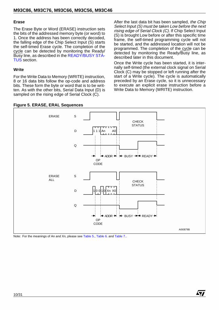
Erase
The Erase Byte or Word (ERASE) instruction setsthe bits of the addressed memory byte (or word) to1. Once the address has been correctly decoded,the falling edge of the Chip Select Input (S) startsthe self-timed Erase cycle. The completion of thecycle can be detected by monitoring the Ready/Busy line, as described in the READY/BUSY STA-TUS section.
Write
For the Write Data to Memory (WRITE) instruction,8 or 16 data bits follow the op-code and addressbits. These form the byte or word that is to be writ-ten. As with the other bits, Serial Data Input (D) issampled on the rising edge of Serial Clock (C).
After the last data bit has been sampled, the ChipSelect Input (S) must be taken Low before the nextrising edge of Serial Clock (C). If Chip Select Input(S) is brought Low before or after this specific timeframe, the self-timed programming cycle will notbe started, and the addressed location will not beprogrammed. The completion of the cycle can bedetected by monitoring the Ready/Busy line, asdescribed later in this document.Once the Write cycle has been started, it is inter-nally self-timed (the external clock signal on SerialClock (C) may be stopped or left running after thestart of a Write cycle). The cycle is automaticallypreceded by an Erase cycle, so it is unnecessaryto execute an explicit erase instruction before aWrite Data to Memory (WRITE) instruction.
Figure 5. ERASE, ERAL Sequences
Note: For the meanings of An and Xn, please see Table 5., Table 6. and Table 7..
AI00879B
SERASE
1 1D
Q
ADDROP
CODE
1
BUSY READY
CHECKSTATUS
SERASEALL
1 0D
Q
OPCODE
1
BUSY READY
CHECKSTATUS
0 0
An A0
Xn X0
ADDR
11/31
M93C86, M93C76, M93C66, M93C56, M93C46
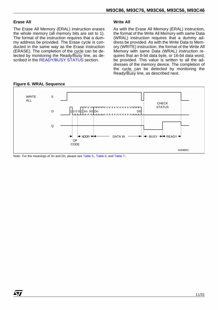
Erase All
The Erase All Memory (ERAL) instruction erasesthe whole memory (all memory bits are set to 1).The format of the instruction requires that a dum-my address be provided. The Erase cycle is con-ducted in the same way as the Erase instruction(ERASE). The completion of the cycle can be de-tected by monitoring the Ready/Busy line, as de-scribed in the READY/BUSY STATUS section.
Write All
As with the Erase All Memory (ERAL) instruction,the format of the Write All Memory with same Data(WRAL) instruction requires that a dummy ad-dress be provided. As with the Write Data to Mem-ory (WRITE) instruction, the format of the Write AllMemory with same Data (WRAL) instruction re-quires that an 8-bit data byte, or 16-bit data word,be provided. This value is written to all the ad-dresses of the memory device. The completion ofthe cycle can be detected by monitoring theReady/Busy line, as described next.
Figure 6. WRAL Sequence
Note: For the meanings of Xn and Dn, please see Table 5., Table 6. and Table 7..
AI00880C
SWRITEALL
DATA IN
D
Q
ADDROP
CODE
Dn D0
BUSY READY
CHECKSTATUS
1 0 00 1 Xn X0
M93C86, M93C76, M93C66, M93C56, M93C46
12/31
READY/BUSY STATUSWhile the Write or Erase cycle is underway, for aWRITE, ERASE, WRAL or ERAL instruction, theBusy signal (Q=0) is returned whenever Chip Se-lect Input (S) is driven High. (Please note, though,that there is an initial delay, of tSLSH, before thisstatus information becomes available). In thisstate, the M93Cx6 ignores any data on the bus.
When the Write cycle is completed, and Chip Se-lect Input (S) is driven High, the Ready signal(Q=1) indicates that the M93Cx6 is ready to re-ceive the next instruction. Serial Data Output (Q)remains set to 1 until the Chip Select Input (S) isbrought Low or until a new start bit is decoded.
INITIAL DELIVERY STATEThe device is delivered with all bits in the memoryarray set to 1 (each byte contains FFh).
COMMON I/O OPERATIONSerial Data Output (Q) and Serial Data Input (D)can be connected together, through a current lim-iting resistor, to form a common, single-wire databus. Some precautions must be taken when oper-ating the memory in this way, mostly to prevent ashort circuit current from flowing when the last ad-dress bit (A0) clashes with the first data bit on Se-rial Data Output (Q). Please see the applicationnote AN394 for details.
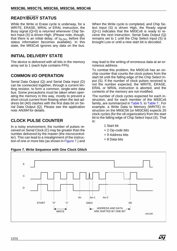
CLOCK PULSE COUNTERIn a noisy environment, the number of pulses re-ceived on Serial Clock (C) may be greater than thenumber delivered by the master (the microcontrol-ler). This can lead to a misalignment of the instruc-tion of one or more bits (as shown in Figure 7.) and
may lead to the writing of erroneous data at an er-roneous address.To combat this problem, the M93Cx6 has an on-chip counter that counts the clock pulses from thestart bit until the falling edge of the Chip Select In-put (S). If the number of clock pulses received isnot the number expected, the WRITE, ERASE,ERAL or WRAL instruction is aborted, and thecontents of the memory are not modified.The number of clock cycles expected for each in-struction, and for each member of the M93Cx6family, are summarized in Table 5. to Table 7.. Forexample, a Write Data to Memory (WRITE) in-struction on the M93C56 (or M93C66) expects 20clock cycles (for the x8 organization) from the startbit to the falling edge of Chip Select Input (S). Thatis:
1 Start bit+ 2 Op-code bits+ 9 Address bits+ 8 Data bits
Figure 7. Write Sequence with One Clock Glitch
AI01395
S
An-1
C
D
WRITE
START D0"1""0"
An
Glitch
An-2
ADDRESS AND DATAARE SHIFTED BY ONE BIT
13/31
M93C86, M93C76, M93C66, M93C56, M93C46
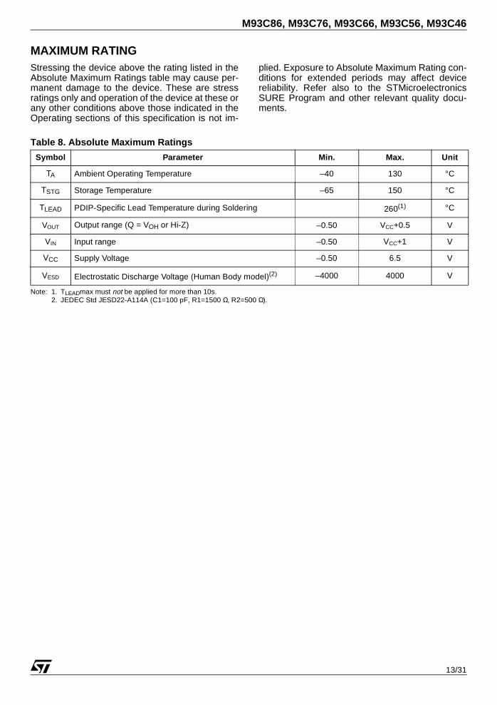
MAXIMUM RATINGStressing the device above the rating listed in theAbsolute Maximum Ratings table may cause per-manent damage to the device. These are stressratings only and operation of the device at these orany other conditions above those indicated in theOperating sections of this specification is not im-
plied. Exposure to Absolute Maximum Rating con-ditions for extended periods may affect devicereliability. Refer also to the STMicroelectronicsSURE Program and other relevant quality docu-ments.
Table 8. Absolute Maximum Ratings
Note: 1. TLEADmax must not be applied for more than 10s.2. JEDEC Std JESD22-A114A (C1=100 pF, R1=1500 Ω, R2=500 Ω).
Symbol Parameter Min. Max. Unit
TA Ambient Operating Temperature –40 130 °C
TSTG Storage Temperature –65 150 °C
TLEAD PDIP-Specific Lead Temperature during Soldering 260(1) °C
VOUT Output range (Q = VOH or Hi-Z) –0.50 VCC+0.5 V
VIN Input range –0.50 VCC+1 V
VCC Supply Voltage –0.50 6.5 V
VESD Electrostatic Discharge Voltage (Human Body model)(2) –4000 4000 V
M93C86, M93C76, M93C66, M93C56, M93C46
14/31
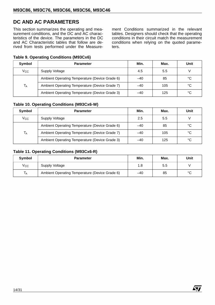
DC AND AC PARAMETERSThis section summarizes the operating and mea-surement conditions, and the DC and AC charac-teristics of the device. The parameters in the DCand AC Characteristic tables that follow are de-rived from tests performed under the Measure-
ment Conditions summarized in the relevanttables. Designers should check that the operatingconditions in their circuit match the measurementconditions when relying on the quoted parame-ters.
Table 9. Operating Conditions (M93Cx6)
Table 10. Operating Conditions (M93Cx6-W)
Table 11. Operating Conditions (M93Cx6-R)
Symbol Parameter Min. Max. Unit
VCC Supply Voltage 4.5 5.5 V
TA
Ambient Operating Temperature (Device Grade 6) –40 85 °C
Ambient Operating Temperature (Device Grade 7) –40 105 °C
Ambient Operating Temperature (Device Grade 3) –40 125 °C
Symbol Parameter Min. Max. Unit
VCC Supply Voltage 2.5 5.5 V
TA
Ambient Operating Temperature (Device Grade 6) –40 85 °C
Ambient Operating Temperature (Device Grade 7) –40 105 °C
Ambient Operating Temperature (Device Grade 3) –40 125 °C
Symbol Parameter Min. Max. Unit
VCC Supply Voltage 1.8 5.5 V
TA Ambient Operating Temperature (Device Grade 6) –40 85 °C

15/31
M93C86, M93C76, M93C66, M93C56, M93C46
Table 12. AC Measurement Conditions (M93Cx6)
Note: 1. Output Hi-Z is defined as the point where data out is no longer driven.
Table 13. AC Measurement Conditions (M93Cx6-W and M93Cx6-R)
Note: 1. Output Hi-Z is defined as the point where data out is no longer driven.
Figure 8. AC Testing Input Output Waveforms
Table 14. Capacitance
Note: Sampled only, not 100% tested, at TA=25°C and a frequency of 1MHz.
Symbol Parameter Min. Max. Unit
CL Load Capacitance 100 pF
Input Rise and Fall Times 50 ns
Input Pulse Voltages 0.4 V to 2.4 V V
Input Timing Reference Voltages 1.0 V and 2.0 V V
Output Timing Reference Voltages 0.8 V and 2.0 V V
Symbol Parameter Min. Max. Unit
CL Load Capacitance 100 pF
Input Rise and Fall Times 50 ns
Input Pulse Voltages 0.2VCC to 0.8VCC V
Input Timing Reference Voltages 0.3VCC to 0.7VCC V
Output Timing Reference Voltages 0.3VCC to 0.7VCC V
Symbol Parameter Test Condition Min Max Unit
COUT OutputCapacitance
VOUT = 0V 5 pF
CIN InputCapacitance
VIN = 0V 5 pF
AI02553
2.4V
0.4V
2.0V
0.8V
2V
1V
INPUT OUTPUT
0.8VCC
0.2VCC
0.7VCC
0.3VCC
M93CXX-W & M93CXX-R
M93CXX

M93C86, M93C76, M93C66, M93C56, M93C46
16/31
Table 15. DC Characteristics (M93Cx6, Device Grade 6)
Table 16. DC Characteristics (M93Cx6, Device Grade 7 or 3)
Symbol Parameter Test Condition Min. Max. Unit
ILI Input Leakage Current 0V ≤ VIN ≤ VCC ±2.5 µA
ILO Output Leakage Current 0V ≤ VOUT ≤ VCC, Q in Hi-Z ±2.5 µA
ICC Supply Current VCC = 5V, S = VIH, f = 2 MHz, Q = open 2 mA
ICC1 Supply Current (Stand-by) VCC = 5V, S = VSS, C = VSS,
ORG = VSS or VCC 15 µA
VIL Input Low Voltage VCC = 5V ± 10% –0.45 0.8 V
VIH Input High Voltage VCC = 5V ± 10% 2 VCC + 1 V
VOL Output Low Voltage VCC = 5V, IOL = 2.1mA 0.4 V
VOH Output High Voltage VCC = 5V, IOH = –400µA 2.4 V
Symbol Parameter Test Condition Min. Max. Unit
ILI Input Leakage Current 0V ≤ VIN ≤ VCC ±2.5 µA
ILO Output Leakage Current 0V ≤ VOUT ≤ VCC, Q in Hi-Z ±2.5 µA
ICC Supply Current VCC = 5V, S = VIH, f = 2 MHz, , Q = open 2 mA
ICC1 Supply Current (Stand-by) VCC = 5V, S = VSS, C = VSS,
ORG = VSS or VCC 15 µA
VIL Input Low Voltage VCC = 5V ± 10% –0.45 0.8 V
VIH Input High Voltage VCC = 5V ± 10% 2 VCC + 1 V
VOL Output Low Voltage VCC = 5V, IOL = 2.1mA 0.4 V
VOH Output High Voltage VCC = 5V, IOH = –400µA 2.4 V
17/31
M93C86, M93C76, M93C66, M93C56, M93C46
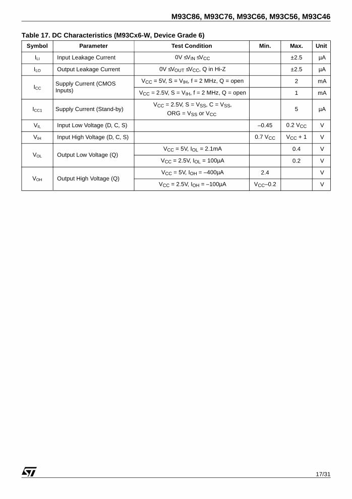
Table 17. DC Characteristics (M93Cx6-W, Device Grade 6)
Symbol Parameter Test Condition Min. Max. Unit
ILI Input Leakage Current 0V ≤ VIN ≤ VCC ±2.5 µA
ILO Output Leakage Current 0V ≤ VOUT ≤ VCC, Q in Hi-Z ±2.5 µA
ICCSupply Current (CMOS Inputs)
VCC = 5V, S = VIH, f = 2 MHz, Q = open 2 mA
VCC = 2.5V, S = VIH, f = 2 MHz, Q = open 1 mA
ICC1 Supply Current (Stand-by) VCC = 2.5V, S = VSS, C = VSS,
ORG = VSS or VCC 5 µA
VIL Input Low Voltage (D, C, S) –0.45 0.2 VCC V
VIH Input High Voltage (D, C, S) 0.7 VCC VCC + 1 V
VOL Output Low Voltage (Q) VCC = 5V, IOL = 2.1mA 0.4 V
VCC = 2.5V, IOL = 100µA 0.2 V
VOH Output High Voltage (Q) VCC = 5V, IOH = –400µA 2.4 V
VCC = 2.5V, IOH = –100µA VCC–0.2 V
M93C86, M93C76, M93C66, M93C56, M93C46
18/31
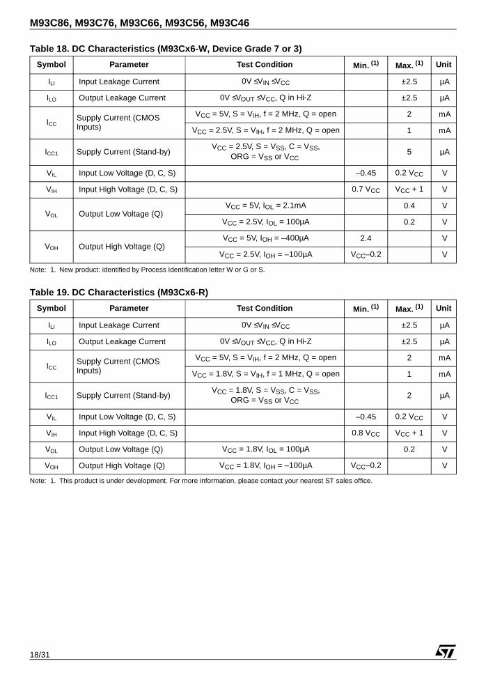
Table 18. DC Characteristics (M93Cx6-W, Device Grade 7 or 3)
Note: 1. New product: identified by Process Identification letter W or G or S.
Table 19. DC Characteristics (M93Cx6-R)
Note: 1. This product is under development. For more information, please contact your nearest ST sales office.
Symbol Parameter Test Condition Min. (1) Max. (1) Unit
ILI Input Leakage Current 0V ≤ VIN ≤ VCC ±2.5 µA
ILO Output Leakage Current 0V ≤ VOUT ≤ VCC, Q in Hi-Z ±2.5 µA
ICCSupply Current (CMOS Inputs)
VCC = 5V, S = VIH, f = 2 MHz, Q = open 2 mA
VCC = 2.5V, S = VIH, f = 2 MHz, Q = open 1 mA
ICC1 Supply Current (Stand-by) VCC = 2.5V, S = VSS, C = VSS,
ORG = VSS or VCC 5 µA
VIL Input Low Voltage (D, C, S) –0.45 0.2 VCC V
VIH Input High Voltage (D, C, S) 0.7 VCC VCC + 1 V
VOL Output Low Voltage (Q) VCC = 5V, IOL = 2.1mA 0.4 V
VCC = 2.5V, IOL = 100µA 0.2 V
VOH Output High Voltage (Q) VCC = 5V, IOH = –400µA 2.4 V
VCC = 2.5V, IOH = –100µA VCC–0.2 V
Symbol Parameter Test Condition Min. (1) Max. (1) Unit
ILI Input Leakage Current 0V ≤ VIN ≤ VCC ±2.5 µA
ILO Output Leakage Current 0V ≤ VOUT ≤ VCC, Q in Hi-Z ±2.5 µA
ICCSupply Current (CMOS Inputs)
VCC = 5V, S = VIH, f = 2 MHz, Q = open 2 mA
VCC = 1.8V, S = VIH, f = 1 MHz, Q = open 1 mA
ICC1 Supply Current (Stand-by) VCC = 1.8V, S = VSS, C = VSS,
ORG = VSS or VCC 2 µA
VIL Input Low Voltage (D, C, S) –0.45 0.2 VCC V
VIH Input High Voltage (D, C, S) 0.8 VCC VCC + 1 V
VOL Output Low Voltage (Q) VCC = 1.8V, IOL = 100µA 0.2 V
VOH Output High Voltage (Q) VCC = 1.8V, IOH = –100µA VCC–0.2 V

19/31
M93C86, M93C76, M93C66, M93C56, M93C46
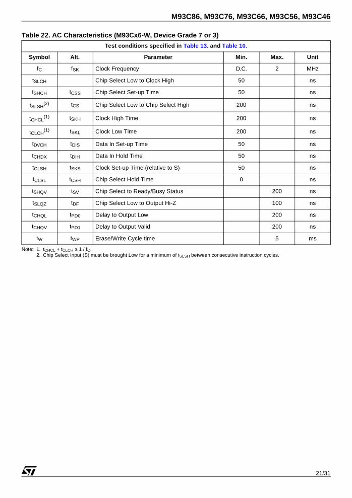
Table 20. AC Characteristics (M93Cx6, Device Grade 6, 7 or 3)
Note: 1. tCHCL + tCLCH ≥ 1 / fC.2. Chip Select Input (S) must be brought Low for a minimum of tSLSH between consecutive instruction cycles.
Test conditions specified in Table 12. and Table 9.
Symbol Alt. Parameter Min. Max. Unit
fC fSK Clock Frequency D.C. 2 MHz
tSLCH Chip Select Low to Clock High 50 ns
tSHCH tCSS
Chip Select Set-up TimeM93C46, M93C56, M93C66 50 ns
Chip Select Set-up timeM93C76, M93C86 50 ns
tSLSH(2) tCS Chip Select Low to Chip Select High 200 ns
tCHCL(1) tSKH Clock High Time 200 ns
tCLCH(1) tSKL Clock Low Time 200 ns
tDVCH tDIS Data In Set-up Time 50 ns
tCHDX tDIH Data In Hold Time 50 ns
tCLSH tSKS Clock Set-up Time (relative to S) 50 ns
tCLSL tCSH Chip Select Hold Time 0 ns
tSHQV tSV Chip Select to Ready/Busy Status 200 ns
tSLQZ tDF Chip Select Low to Output Hi-Z 100 ns
tCHQL tPD0 Delay to Output Low 200 ns
tCHQV tPD1 Delay to Output Valid 200 ns
tW tWP Erase/Write Cycle time 5 ms

M93C86, M93C76, M93C66, M93C56, M93C46
20/31
Table 21. AC Characteristics (M93Cx6-W, Device Grade 6)
Note: 1. tCHCL + tCLCH ≥ 1 / fC.2. Chip Select Input (S) must be brought Low for a minimum of tSLSH between consecutive instruction cycles.
Test conditions specified in Table 13. and Table 10.
Symbol Alt. Parameter Min. Max. Unit
fC fSK Clock Frequency D.C. 2 MHz
tSLCH Chip Select Low to Clock High 50 ns
tSHCH tCSS Chip Select Set-up Time 50 ns
tSLSH(2) tCS Chip Select Low to Chip Select High 200 ns
tCHCL(1) tSKH Clock High Time 200 ns
tCLCH(1) tSKL Clock Low Time 200 ns
tDVCH tDIS Data In Set-up Time 50 ns
tCHDX tDIH Data In Hold Time 50 ns
tCLSH tSKS Clock Set-up Time (relative to S) 50 ns
tCLSL tCSH Chip Select Hold Time 0 ns
tSHQV tSV Chip Select to Ready/Busy Status 200 ns
tSLQZ tDF Chip Select Low to Output Hi-Z 100 ns
tCHQL tPD0 Delay to Output Low 200 ns
tCHQV tPD1 Delay to Output Valid 200 ns
tW tWP Erase/Write Cycle time 5 ms
21/31
M93C86, M93C76, M93C66, M93C56, M93C46
Table 22. AC Characteristics (M93Cx6-W, Device Grade 7 or 3)
Note: 1. tCHCL + tCLCH ≥ 1 / fC.2. Chip Select Input (S) must be brought Low for a minimum of tSLSH between consecutive instruction cycles.
Test conditions specified in Table 13. and Table 10.
Symbol Alt. Parameter Min. Max. Unit
fC fSK Clock Frequency D.C. 2 MHz
tSLCH Chip Select Low to Clock High 50 ns
tSHCH tCSS Chip Select Set-up Time 50 ns
tSLSH(2) tCS Chip Select Low to Chip Select High 200 ns
tCHCL(1) tSKH Clock High Time 200 ns
tCLCH(1) tSKL Clock Low Time 200 ns
tDVCH tDIS Data In Set-up Time 50 ns
tCHDX tDIH Data In Hold Time 50 ns
tCLSH tSKS Clock Set-up Time (relative to S) 50 ns
tCLSL tCSH Chip Select Hold Time 0 ns
tSHQV tSV Chip Select to Ready/Busy Status 200 ns
tSLQZ tDF Chip Select Low to Output Hi-Z 100 ns
tCHQL tPD0 Delay to Output Low 200 ns
tCHQV tPD1 Delay to Output Valid 200 ns
tW tWP Erase/Write Cycle time 5 ms

M93C86, M93C76, M93C66, M93C56, M93C46
22/31
Table 23. AC Characteristics (M93Cx6-R)
Note: 1. tCHCL + tCLCH ≥ 1 / fC.2. Chip Select Input (S) must be brought Low for a minimum of tSLSH between consecutive instruction cycles.3. This product is under development. For more information, please contact your nearest ST sales office.
Test conditions specified in Table 13. and Table 11.
Symbol Alt. Parameter Min.(3) Max.(3) Unit
fC fSK Clock Frequency D.C. 1 MHz
tSLCH Chip Select Low to Clock High 250 ns
tSHCH tCSS Chip Select Set-up Time 50 ns
tSLSH(2) tCS Chip Select Low to Chip Select High 250 ns
tCHCL(1) tSKH Clock High Time 250 ns
tCLCH(1) tSKL Clock Low Time 250 ns
tDVCH tDIS Data In Set-up Time 100 ns
tCHDX tDIH Data In Hold Time 100 ns
tCLSH tSKS Clock Set-up Time (relative to S) 100 ns
tCLSL tCSH Chip Select Hold Time 0 ns
tSHQV tSV Chip Select to Ready/Busy Status 400 ns
tSLQZ tDF Chip Select Low to Output Hi-Z 200 ns
tCHQL tPD0 Delay to Output Low 400 ns
tCHQV tPD1 Delay to Output Valid 400 ns
tW tWP Erase/Write Cycle time 10 ms

23/31
M93C86, M93C76, M93C66, M93C56, M93C46
Figure 9. Synchronous Timing (Start and Op-Code Input)
Figure 10. Synchronous Timing (Read or Write)
Figure 11. Synchronous Timing (Read or Write)
AI01428
C
OP CODE OP CODESTART
S
D
OP CODE INPUTSTART
tDVCH
tSHCH
tCLSH tCHCL
tCLCH
tCHDX
AI00820C
C
D
Q
ADDRESS INPUT
Hi-Z
tDVCH
tCLSL
A0
S
DATA OUTPUT
tCHQVtCHDX
tCHQL
An
tSLSH
tSLQZ
Q15/Q7 Q0
AI01429
C
D
Q
ADDRESS/DATA INPUT
Hi-Z
tDVCH
tSLCH
A0/D0
S
WRITE CYCLE
tSLSHtCHDX
An
tCLSL
tSLQZ
BUSY
tSHQV
tW
READY

M93C86, M93C76, M93C66, M93C56, M93C46
24/31
PACKAGE MECHANICAL
Figure 12. PDIP8 – 8 pin Plastic DIP, 0.25mm lead frame, Package Outline
Note: Drawing is not to scale.
Table 24. PDIP8 – 8 pin Plastic DIP, 0.25mm lead frame, Package Mechanical Data
Symbolmillimeters inches
Typ. Min. Max. Typ. Min. Max.
A 5.33 0.210
A1 0.38 0.015
A2 3.30 2.92 4.95 0.130 0.115 0.195
b 0.46 0.36 0.56 0.018 0.014 0.022
b2 1.52 1.14 1.78 0.060 0.045 0.070
c 0.25 0.20 0.36 0.010 0.008 0.014
D 9.27 9.02 10.16 0.365 0.355 0.400
E 7.87 7.62 8.26 0.310 0.300 0.325
E1 6.35 6.10 7.11 0.250 0.240 0.280
e 2.54 – – 0.100 – –
eA 7.62 – – 0.300 – –
eB 10.92 0.430
L 3.30 2.92 3.81 0.130 0.115 0.150
PDIP-B
A2
A1
A
L
b e
D
E1
8
1
ceA
b2
eB
E

25/31
M93C86, M93C76, M93C66, M93C56, M93C46
Figure 13. SO8 narrow – 8 lead Plastic Small Outline, 150 mils body width, Package Outline
Note: Drawing is not to scale.
Table 25. SO8 narrow – 8 lead Plastic Small Outline, 150 mils body width, Package Data
Symbolmillimeters inches
Typ Min Max Typ Min Max
A 1.35 1.75 0.053 0.069
A1 0.10 0.25 0.004 0.010
A2 1.10 1.65 0.043 0.065
B 0.33 0.51 0.013 0.020
C 0.19 0.25 0.007 0.010
D 4.80 5.00 0.189 0.197
ddd 0.10 0.004
E 3.80 4.00 0.150 0.157
e 1.27 – – 0.050 – –
H 5.80 6.20 0.228 0.244
h 0.25 0.50 0.010 0.020
L 0.40 0.90 0.016 0.035
α 0° 8° 0° 8°
N (pin number) 8 8
SO-A
E
8
dddB
e
A
D
C
LA1 α1
H
h x 45˚
A2

M93C86, M93C76, M93C66, M93C56, M93C46
26/31
Figure 14. UFDFPN8 (MLP8) 8-lead Ultra thin Fine pitch Dual Flat Package No lead 2x3mm²,Outline
Note: 1. Drawing is not to scale.2. The central pad (the area E2 by D2 in the above illustration) is pulled, internally, to VSS. It must not be allowed to be connected to
any other voltage or signal line on the PCB, for example during the soldering process.
Table 26. UFDFPN8 (MLP8) 8-lead Ultra thin Fine pitch Dual Flat Package No lead 2x3mm², Data
Symbolmillimeters inches
Typ. Min. Max. Typ. Min. Max.
A 0.55 0.50 0.60 0.022 0.020 0.024
A1 0.00 0.05 0.000 0.002
b 0.25 0.20 0.30 0.010 0.008 0.012
D 2.00 0.079
D2 1.55 1.65 0.061 0.065
ddd 0.05 0.002
E 3.00 0.118
E2 0.15 0.25 0.006 0.010
e 0.50 – – 0.020 – –
L 0.45 0.40 0.50 0.018 0.016 0.020
L1 0.15 0.006
L3 0.30 0.012
N (pin number) 8 8
D
E
UFDFPN-01
A
A1ddd
L1
e b
D2
L
E2
L3

27/31
M93C86, M93C76, M93C66, M93C56, M93C46
Figure 15. TSSOP8 3x3mm² – 8 lead Thin Shrink Small Outline, 3x3mm² body size, PackageOutline
Note: Drawing is not to scale.
Table 27. TSSOP8 3x3mm² – 8 lead Thin Shrink Small Outline, 3x3mm² body size,Mechanical Data
Symbolmillimeters inches
Typ. Min. Max. Typ. Min. Max.
A 1.100 0.0433
A1 0.050 0.150 0.0020 0.0059
A2 0.850 0.750 0.950 0.0335 0.0295 0.0374
b 0.250 0.400 0.0098 0.0157
c 0.130 0.230 0.0051 0.0091
D 3.000 2.900 3.100 0.1181 0.1142 0.1220
E 4.900 4.650 5.150 0.1929 0.1831 0.2028
E1 3.000 2.900 3.100 0.1181 0.1142 0.1220
e 0.650 – – 0.0256 – –
CP 0.100 0.0039
L 0.550 0.400 0.700 0.0217 0.0157 0.0276
L1 0.950 0.0374
α 0° 6° 0° 6°
N (pin number) 8 8
TSSOP8BM
1
8
CP
c
L
EE1
D
A2A
α
eb
4
5
A1
L1

M93C86, M93C76, M93C66, M93C56, M93C46
28/31
Figure 16. TSSOP8 – 8 lead Thin Shrink Small Outline, Package Outline
Note: Drawing is not to scale.
Table 28. TSSOP8 – 8 lead Thin Shrink Small Outline, Package Mechanical Data
Symbolmillimeters inches
Typ. Min. Max. Typ. Min. Max.
A 1.200 0.0472
A1 0.050 0.150 0.0020 0.0059
A2 1.000 0.800 1.050 0.0394 0.0315 0.0413
b 0.190 0.300 0.0075 0.0118
c 0.090 0.200 0.0035 0.0079
CP 0.100 0.0039
D 3.000 2.900 3.100 0.1181 0.1142 0.1220
e 0.650 – – 0.0256 – –
E 6.400 6.200 6.600 0.2520 0.2441 0.2598
E1 4.400 4.300 4.500 0.1732 0.1693 0.1772
L 0.600 0.450 0.750 0.0236 0.0177 0.0295
L1 1.000 0.0394
α 0° 8° 0° 8°
N (pin number) 8 8
TSSOP8AM
1
8
CP
c
L
EE1
D
A2A
α
eb
4
5
A1
L1
29/31
M93C86, M93C76, M93C66, M93C56, M93C46
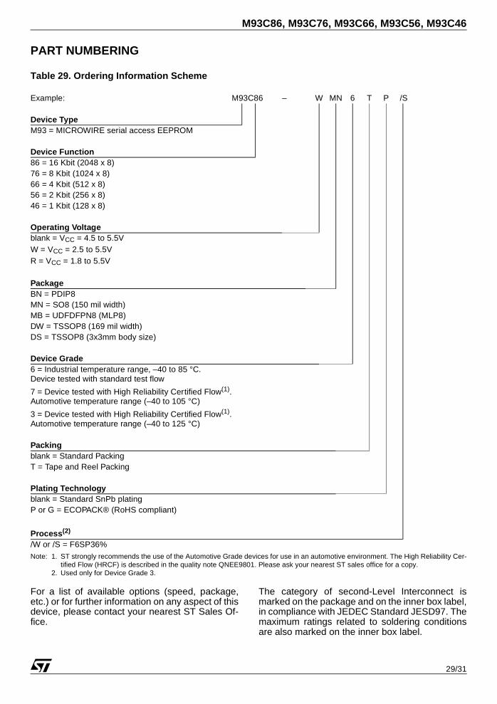
PART NUMBERING
Table 29. Ordering Information Scheme
Note: 1. ST strongly recommends the use of the Automotive Grade devices for use in an automotive environment. The High Reliability Cer-tified Flow (HRCF) is described in the quality note QNEE9801. Please ask your nearest ST sales office for a copy.
2. Used only for Device Grade 3.
For a list of available options (speed, package,etc.) or for further information on any aspect of thisdevice, please contact your nearest ST Sales Of-fice.
The category of second-Level Interconnect ismarked on the package and on the inner box label,in compliance with JEDEC Standard JESD97. Themaximum ratings related to soldering conditionsare also marked on the inner box label.
Example: M93C86 – W MN 6 T P /S
Device TypeM93 = MICROWIRE serial access EEPROM
Device Function86 = 16 Kbit (2048 x 8)76 = 8 Kbit (1024 x 8)66 = 4 Kbit (512 x 8)56 = 2 Kbit (256 x 8)46 = 1 Kbit (128 x 8)
Operating Voltageblank = VCC = 4.5 to 5.5VW = VCC = 2.5 to 5.5VR = VCC = 1.8 to 5.5V
PackageBN = PDIP8MN = SO8 (150 mil width)MB = UDFDFPN8 (MLP8)DW = TSSOP8 (169 mil width)DS = TSSOP8 (3x3mm body size)
Device Grade6 = Industrial temperature range, –40 to 85 °C.Device tested with standard test flow
7 = Device tested with High Reliability Certified Flow(1).Automotive temperature range (–40 to 105 °C)
3 = Device tested with High Reliability Certified Flow(1).Automotive temperature range (–40 to 125 °C)
Packingblank = Standard PackingT = Tape and Reel Packing
Plating Technologyblank = Standard SnPb platingP or G = ECOPACK® (RoHS compliant)
Process(2)
/W or /S = F6SP36%

M93C86, M93C76, M93C66, M93C56, M93C46
30/31
REVISION HISTORY
Table 30. Document Revision History
Date Rev. Description of Revision
04-Feb-2003 2.0
Document reformatted, and reworded, using the new template. Temperature range 1 removed. TSSOP8 (3x3mm) package added. New products, identified by the process letter W, added, with fc(max) increased to 1MHz for -R voltage range, and to 2MHz for all other ranges (and corresponding parameters adjusted)
26-Mar-2003 2.1Value of standby current (max) corrected in DC characteristics tables for -W and -R rangesVOUT and VIN separated from VIO in the Absolute Maximum Ratings table
04-Apr-2003 2.2Values corrected in AC characteristics tables for -W range (tSLSH, tDVCH, tCLSL) for devices with Process Identification Letter W
23-May-2003 2.3 Standby current corrected for -R range
27-May-2003 2.4 Turned-die option re-instated in Ordering Information Scheme
25-Nov-2003 3.0Table of contents, and Pb-free options added. Temperature range 7 added. VIL(min) improved to –0.45V.
30-Mar-2004 4.0MLP package added. Absolute Maximum Ratings for VIO(min) and VCC(min) changed. Soldering temperature information clarified for RoHS compliant devices. Device grade information clarified. Process identification letter “G” information added
16-Aug-2004 5.0 M93C06 removed. Device grade information further clarified. Process identification letter “S” information added. Turned-die package option removed. Product list summary added.
27-Oct-2005 6.0
current product/new product distinction removed. ICC and ICC1 values for current product removed from tables 15, 16 and 17 and AC characteristics for current product removed from Tables 20 and 21. Clock rate added to FEATURES SUMMARY.“Q = open” added to ICC Test conditions in DC Characteristics Tables 15, 16, 17, 18 and 19.
Process(2) added to Table 29., Ordering Information Scheme. POWER ON DATA PROTECTION section removed, replaced by INTERNAL DEVICE RESET and ACTIVE POWER AND STANDBY POWER MODES. INITIAL DELIVERY STATE added.SO8N and TSSOP8 packages updated. PDIP-specific TLEAD added to Table 8., Absolute Maximum Ratings.
31/31
M93C86, M93C76, M93C66, M93C56, M93C46
Information furnished is believed to be accurate and reliable. However, STMicroelectronics assumes no responsibility for the consequences of use of such information nor for any infringement of patents or other rights of third parties which may result from its use. No license is granted by implication or otherwise under any patent or patent rights of STMicroelectronics. Specifications mentioned in this publication are subject to change without notice. This publication supersedes and replaces all information previously supplied. STMicroelectronics products are not
authorized for use as critical components in life support devices or systems without express written approval of STMicroelectronics.
The ST logo is a registered trademark of STMicroelectronics.
All other names are the property of their respective owners
© 2005 STMicroelectronics - All rights reserved
STMicroelectronics group of companiesAustralia - Belgium - Brazil - Canada - China - Czech Republic - Finland - France - Germany - Hong Kong - India - Israel - Italy - Japan -
Malaysia - Malta - Morocco - Singapore - Spain - Sweden - Switzerland - United Kingdom - United States of Americawww.st.com