DISSERTATION DOKTOR-INGENIEURS (DR.-ING.) - Uni Ulm
225
High-Linearity Receivers for Mobile Communication Applications using SiGe Technology DISSERTATION Zur Erlangung des akademischen Grades eines DOKTOR-INGENIEURS (DR.-ING.) der Fakult¨ at f¨ur Ingenieurwissenschaften und Informatik der Universit¨ at Ulm von Frank Gruson aus Heidenheim 1. Gutachter: Prof. Dr.-Ing. Hermann Schumacher 2. Gutachter: Prof. Dr.-Ing. Joachim Burghartz Amtierender Dekan: Prof. Dr.-Ing. Michael Weber Ulm, 10.06.2010
Transcript of DISSERTATION DOKTOR-INGENIEURS (DR.-ING.) - Uni Ulm
High-Linearity Receiversfor Mobile Communication Applications
using SiGe Technology
DISSERTATION
Zur Erlangung des akademischen Grades eines
DOKTOR-INGENIEURS(DR.-ING.)
der Fakultat fur Ingenieurwissenschaften
und Informatik der Universitat Ulm
von
Frank Grusonaus Heidenheim
1. Gutachter: Prof. Dr.-Ing. Hermann Schumacher
2. Gutachter: Prof. Dr.-Ing. Joachim Burghartz
Amtierender Dekan: Prof. Dr.-Ing. Michael Weber
Ulm, 10.06.2010

2
Applying the calculus concept of limits,the specialist gets to know more and moreabout less and less until, in the limit,he retires, knowing everything about nothing.The generalist learns less and lessabout more and more until, in the limit,he retires, knowing nothing about everything.Neither is quite the ideal life.
Lawrence J. Kamm
CONTENTS i
Contents
1 Introduction 1
2 Introduction to mobile communication systems 2
2.1 Digital modulation and the need for linear receive front-ends . . . . . . . . 2
2.2 Mobile phone standards . . . . . . . . . . . . . . . . . . . . . . . . . . . . 5
2.2.1 The evolution of mobile communications . . . . . . . . . . . . . . . 5
2.2.2 CDMA . . . . . . . . . . . . . . . . . . . . . . . . . . . . . . . . . . 5
2.2.3 Narrow-band CDMA . . . . . . . . . . . . . . . . . . . . . . . . . . 6
2.2.4 Wide band CDMA (UMTS) . . . . . . . . . . . . . . . . . . . . . . 7
2.3 Professional mobile radio systems . . . . . . . . . . . . . . . . . . . . . . . 10
2.4 Wireless Local Area Networks . . . . . . . . . . . . . . . . . . . . . . . . . 11
2.5 Global Positioning Systems . . . . . . . . . . . . . . . . . . . . . . . . . . 14
3 System considerations and level planning 16
3.1 Intermodulation distortion . . . . . . . . . . . . . . . . . . . . . . . . . . . 18
3.1.1 Derivation of LNA IIP3 requirements . . . . . . . . . . . . . . . . . 22
3.1.2 Derivation of receiver NF requirements . . . . . . . . . . . . . . . . 24
4 Device technology 26
4.1 Technology selection criteria . . . . . . . . . . . . . . . . . . . . . . . . . . 26
4.2 SiGe1 and SiGe2 bipolar processes . . . . . . . . . . . . . . . . . . . . . . 26
4.3 SiGe1 model verification . . . . . . . . . . . . . . . . . . . . . . . . . . . . 27
4.4 at46000 SiGe BiCMOS process . . . . . . . . . . . . . . . . . . . . . . . . 31
4.5 Atmel’s at46000 0.35µm CMOS technology . . . . . . . . . . . . . . . . . . 32
4.6 Packaging . . . . . . . . . . . . . . . . . . . . . . . . . . . . . . . . . . . . 34
5 Modelling of passive components 36
5.1 Passive components on Silicon substrates . . . . . . . . . . . . . . . . . . . 36
5.2 Lumped element circuit design . . . . . . . . . . . . . . . . . . . . . . . . . 36
5.3 Loss mechanisms of passive components on silicon . . . . . . . . . . . . . . 37
5.4 Spiral inductors in the Atmel SiGe1 and SiGe2 processes . . . . . . . . . . 38
5.5 Equivalent circuit extraction . . . . . . . . . . . . . . . . . . . . . . . . . . 41
ii CONTENTS
5.6 Definition of the ’quality factor’ . . . . . . . . . . . . . . . . . . . . . . . . 44
5.7 The choice of the metal layers . . . . . . . . . . . . . . . . . . . . . . . . . 46
5.8 Influence of the via geometry . . . . . . . . . . . . . . . . . . . . . . . . . 47
5.9 Inductors on high resistivity substrates . . . . . . . . . . . . . . . . . . . . 48
5.10 The channel stopper . . . . . . . . . . . . . . . . . . . . . . . . . . . . . . 49
5.11 Influence of the substrate . . . . . . . . . . . . . . . . . . . . . . . . . . . . 50
5.12 Improving Q factor and reducing crosstalk by patterned ground shields . . 52
5.13 Electromagnetic field simulation . . . . . . . . . . . . . . . . . . . . . . . . 55
5.13.1 2.5D simulators based on the method of moments . . . . . . . . . . 55
5.13.2 Why a planar inductor is not a two-dimensional structure . . . . . . 56
5.13.3 Sensitivity of the EM simulation . . . . . . . . . . . . . . . . . . . . 60
5.13.4 Comparison of 2.5D and 3D EM simulators . . . . . . . . . . . . . 61
5.14 Analysis of process spreads . . . . . . . . . . . . . . . . . . . . . . . . . . . 62
5.15 Modelling . . . . . . . . . . . . . . . . . . . . . . . . . . . . . . . . . . . . 64
5.16 Multilevel spiral inductors . . . . . . . . . . . . . . . . . . . . . . . . . . . 70
5.17 Symmetrical, centre-tapped inductors . . . . . . . . . . . . . . . . . . . . . 70
6 The low noise amplifier 75
6.1 Harold Black and the negative feedback amplifier . . . . . . . . . . . . . . 75
6.2 Broadband LNA designs . . . . . . . . . . . . . . . . . . . . . . . . . . . . 75
6.2.1 Transimpedance amplifier . . . . . . . . . . . . . . . . . . . . . . . 75
6.2.2 Darlington circuits . . . . . . . . . . . . . . . . . . . . . . . . . . . 79
6.2.3 Transformer based LNAs . . . . . . . . . . . . . . . . . . . . . . . . 81
6.3 Simultaneous noise and power match in narrowband LNAs . . . . . . . . . 82
6.3.1 Application to CMOS LNAs . . . . . . . . . . . . . . . . . . . . . . 88
6.4 Bias considerations . . . . . . . . . . . . . . . . . . . . . . . . . . . . . . . 88
6.5 The influence of bias conditions on linearity . . . . . . . . . . . . . . . . . 93
6.6 Effect of series and parallel feedback on noise figure and linearity . . . . . . 95
6.7 Linearity considerations for bipolar transistors . . . . . . . . . . . . . . . . 96
6.7.1 Analytical considerations . . . . . . . . . . . . . . . . . . . . . . . . 96
6.7.2 Linearisation by series feedback . . . . . . . . . . . . . . . . . . . . 98
6.8 LNA circuit implementations . . . . . . . . . . . . . . . . . . . . . . . . . 102
6.8.1 Influence of bias resistor . . . . . . . . . . . . . . . . . . . . . . . . 102

CONTENTS iii
6.8.2 Broadband source termination . . . . . . . . . . . . . . . . . . . . . 102
6.8.3 Low frequency termination using LC trap networks . . . . . . . . . 103
6.8.4 Low frequency termination using bias inductors and a diode . . . . 105
6.8.5 Low frequency termination using active bias networks . . . . . . . . 112
6.8.6 CMOS LNA implementations . . . . . . . . . . . . . . . . . . . . . 116
6.8.7 Cancellation by capacitive feedback in narrow band amplifiers . . . 118
6.8.8 Matching networks with notch filters . . . . . . . . . . . . . . . . . 121
6.8.9 Comparison of the circuit design techniques for linearization en-hancement . . . . . . . . . . . . . . . . . . . . . . . . . . . . . . . . 125
7 The downconverter 131
7.1 Super-hetero and direct-conversion receivers . . . . . . . . . . . . . . . . . 131
7.2 Mixing operation . . . . . . . . . . . . . . . . . . . . . . . . . . . . . . . . 132
7.3 Mixers utilising device nonlinearities . . . . . . . . . . . . . . . . . . . . . 133
7.4 Switching mixers . . . . . . . . . . . . . . . . . . . . . . . . . . . . . . . . 133
7.5 Commutating mixers . . . . . . . . . . . . . . . . . . . . . . . . . . . . . . 136
7.5.1 Passive commutating mixer using Schottky Diodes . . . . . . . . . . 137
7.5.2 Passive commutating mixer using FET (NMOS) transistors . . . . . 139
7.6 The Gilbert mixer: An active, commutating mixer . . . . . . . . . . . . . . 140
7.7 Image rejection mixers . . . . . . . . . . . . . . . . . . . . . . . . . . . . . 142
7.8 Mixer summary and conclusions . . . . . . . . . . . . . . . . . . . . . . . . 147
8 Conclusion 149
A Noise figure measurements 152
A.1 General considerations . . . . . . . . . . . . . . . . . . . . . . . . . . . . . 152
A.2 The Gain Method . . . . . . . . . . . . . . . . . . . . . . . . . . . . . . . . 152
A.3 The Y Factor Method . . . . . . . . . . . . . . . . . . . . . . . . . . . . . 153
A.4 Improving measurement accuracy by a low-noise preamplifier . . . . . . . . 157
A.5 Example . . . . . . . . . . . . . . . . . . . . . . . . . . . . . . . . . . . . . 160
B Measuring intermodulation distortion products 162
B.1 Combining the sources . . . . . . . . . . . . . . . . . . . . . . . . . . . . . 162
B.2 Setting up the spectrum analyser . . . . . . . . . . . . . . . . . . . . . . . 163
B.3 Using a frequency translating vector network analyser . . . . . . . . . . . . 163
iv CONTENTS
C On-wafer characterisation of inductors -the measurement challenge 165
C.1 Getting the right contact . . . . . . . . . . . . . . . . . . . . . . . . . . . . 165
C.2 Influence of the coaxial calibration technique . . . . . . . . . . . . . . . . . 165
C.3 Pad removal techniques (de-embedding) . . . . . . . . . . . . . . . . . . . 167
C.4 Wafer level calibration as an alternative to de-embedding . . . . . . . . . . 170
C.5 Choosing the right technique . . . . . . . . . . . . . . . . . . . . . . . . . . 173
C.6 On-wafer characterisation of 3-ports . . . . . . . . . . . . . . . . . . . . . . 173
D Details about the SiGe processes 175
E Detailed schematics and benchmarks 176
F Dimensioning spiral inductors 186
G Glossary of terms 189
H List of symbols 193
References 195
1
1 Introduction
Modern mobile communication systems shaped the semiconductor industry during thelast decade: The demand for lower cost and higher speed at reduced power consump-tion and increased functionality has been a key driver for CMOS technology scaling andeven at today’s gate geometries of 45 nm Moore’s law continues to go on. Alternativetechnologies like Silicon-Germanium Heterobipolar (SiGe HBT) technology displaced es-tablished receiver architectures based on discrete semiconductors and III-V electronicsinto the niche of power-amplifiers and antenna switch modules – before SiGe HBT finallywill be displaced by RF CMOS to higher-frequency applications like automotive radar.This thesis applied a wide range of available circuit design techniques to realize very lin-ear receivers with low noise figure to satisfy the system needs of applications like UMTS,CDMA, GPS, TETRA and WLAN. Circuits have been realized that show comparableor better linearity and noise performance than implementations using discrete or III-Vtechnology. As the author of this thesis escorted SiGe technology from early infancy inthe clean rooms of the Daimler research labs via the production transfer to Temic (laterrenamed Atmel, now TELEFUNKEN Semiconductors [1]) – where he was part of theteam that developed the first commercially available SiGe frontend circuit – a big part ofthis work is dedicated to device modelling. This is essential, as only accurate models en-able the trend to first-time right designs with optimum performance. At Ulm Universityhe joined forces with a team that innovated MMIC design at frequencies up to 24 GHzusing commercially available SiGe HBT production lines from Atmel [2].A good circuit needs to fulfil the requirements of the system, rather than the systemcoping with the limitations of the circuit. Therefore chapter 2 shortly explains the mo-bile communications systems used in this thesis and derives the system requirements forthe receivers to be realized in chapter 3. The common demand of all these systems is:(i) High linearity (ii) Low power consumption and (iii) Low noise figure. While SiGe HBTtechnology allows for the realisation of low-noise, low-power RF circuits, high linearitytypically is achieved by high operating currents. Therefore circuit design techniques werenecessary to satisfy the linearity needs without the use of excessive current. Chapter 4briefly compares the different technologies used, including an experimental verificationof the active device models in the design kit. This is then followed in chapter 5 by anextensive measurement and modelling campaign to remove the deficiency of the passivedevice models in the design kit: After improving both the accuracy of the on-wafer mea-surements (see appendix C) and the quality of the electro-magnetic field simulations,both techniques have been merged to derive a set of scaleable inductor models, greatlyfacilitating RF circuit design at RF frequencies. Chapter 6 is dedicated to the low-noiseamplifier (LNA) and uses circuit design techniques to optimise linearity at a minimum ofnoise and current consumption, followed by extensive benchmarking. Mixer designs areevaluated in chapter 7, identifying different mixer types to optimally serve the require-ments of different systems. The thesis ends up with a conclusion and gives an outlookwhere further studies might be directed to.
2 2 INTRODUCTION TO MOBILE COMMUNICATION SYSTEMS
2 Introduction to mobile communication systems
2.1 Digital modulation and the need for linear receive front-
ends
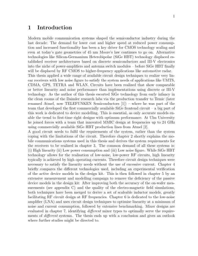
The move from analog phone systems like NMT (Nordic Mobile Telephone) and AMPS(Advanced Mobile Phone System) with AM or FM modulation to digital standards likeGSM and UMTS using digital modulation techniques provides more information capacity,compatibility with digital data services, higher data security and better quality commu-nications. The RF spectrum must be shared, yet every day there are more users for theavailable spectrum as the demand for communications services increases. Digital mod-ulation schemes have greater capacity than analog modulation schemes to convey largeamounts of information. There is a fundamental trade off in communications systems:Simple hardware can be used in transmitter and receivers to communicate information.However, this uses a large amount of spectrum which limits the number of users or theavailable data rates. Pagers, for example, use simple digital modulation algorithms like2-level FSK or BPSK (see Fig. 1) which can be demodulated even deep inside modernsteel/concrete buildings. Alternatively, more complex transmitters and receivers can beused to transmit the same information over less bandwidth. This transition to more andmore spectrally efficient transmission techniques requires more and more complex hard-ware. Complex hardware is difficult to design, test, and build due to more demandingspecifications. [3]. They key specifications which need to be met in a complex receiver arenoise figure, linearity and power consumption.
0
1
0 1 2 3 4
sig
na
l
time
binary signal
−1
0
1
0 1 2 3 4
sig
na
l
time
ASK
−1
0
1
0 1 2 3 4
sig
na
l
time
FSK
−1
0
1
0 1 2 3 4
sig
na
l
time
PSK
Figure 1: Digital bit stream (top left) encoded with simple modulation formatslike Amplitude Shift Keying (ASK), Frequency Shift Keying (FSK) and Phase Shift
Keying (PSK).
2.1 Digital modulation and the need for linear receive front-ends 3
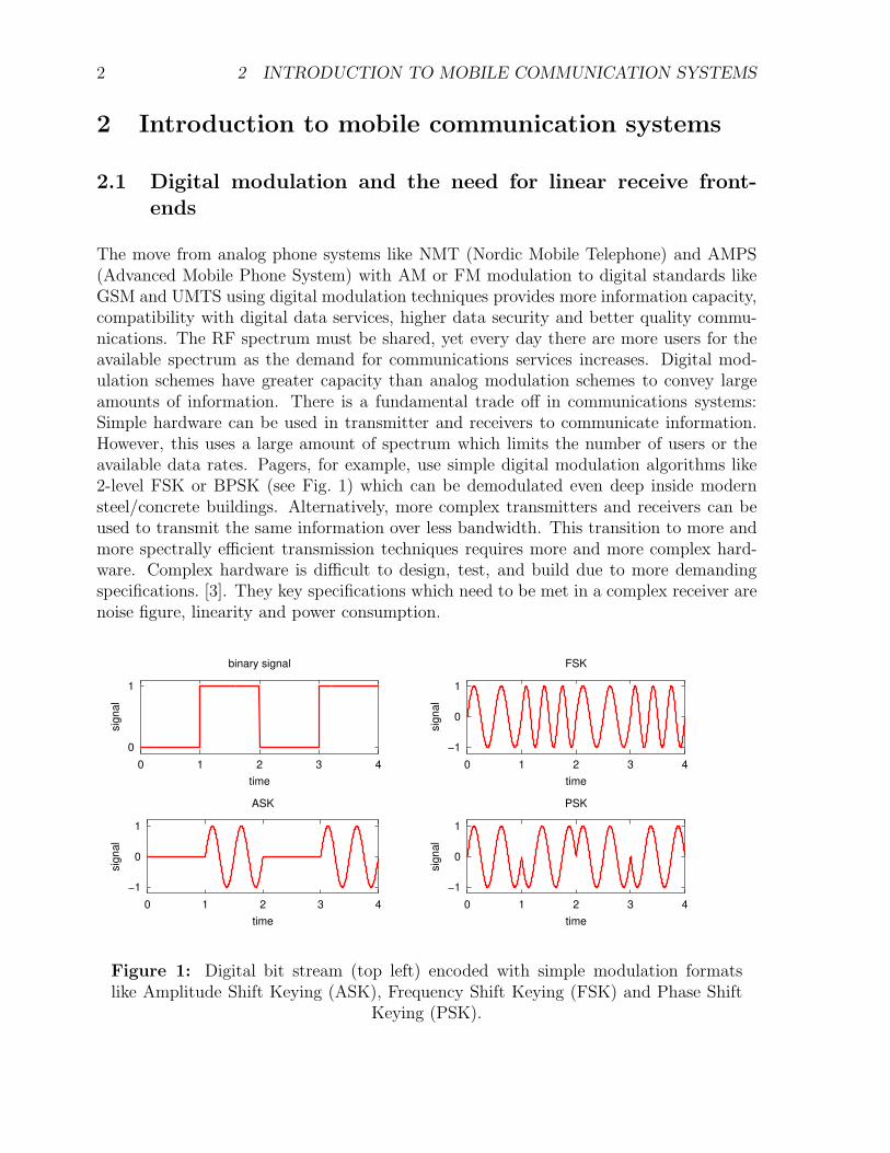
A symbol is defined as a state in the polar IQ plane at a given time (see Fig. 2). The signalbandwidth for the communications channel depends on this symbol rate. BPSK (Bi-PhaseShift Keying) has got 2 states (0 or 180) corresponding to just one bit of information (’0’or ’1’). Here the bit rate just equals the symbol rate, but the states can be distinguished(’demodulated’) easily. This is important for spread-spectrum satellite-based systemslike GPS due to the high attenuation between the transmitter in the satellite and theterrestrial receiver and the fact that the signal level is below the thermal noise floor. Dueto the low bit rate of BPSK, it takes around 35 seconds even with a good sky view untilthe GPS receiver has all the necessary information to calculate a valid position1. A lowreceiver noise figure is important to acquire the weak GPS signals, while linearity is notimportant for stand-alone GPS receivers. However, as most GPS receivers need to workclose to mobile phones that transmit with power levels that are up to 1017 times strongerthan the weak GPS signals at an offset of just 200 MHz, linearity becomes importantfor GPS receivers, too. The GPS system is sketched in section 2.5 and the low-noisepreamplifier developed in this thesis in chapter 6.8.8.
BPSK
0 1
π/4 DQPSK
11 10
01 00
00
11
10
01
GMSK
0 1
QPSK
11 10
01 00
One Bit Per Symbol One Bit Per Symbol Two Bits Per Symbol Two Bits Per Symbol
Figure 2: Digital modulation formats of the systems covered in this thesis shown ina constellation diagram.
In FSK, the frequency of the carrier is changed between two values as a function ofthe modulating signal (data) being transmitted. For Minimum (frequency) Shift Key-ing, MSK, the difference between these two frequencies is chosen to be half the datarate, with the result that the modulated carrier contains no phase discontinuities andfrequency changes occur at the carrier zero crossings (see Fig. 1, top right) [4]. Thus, astatic frequency shift translates into a linearly varying phase shift. This leads to a vectorrotating either clockwise or counterclockwise, the absolute states in the constellation di-agram being irrelevant. A long series of binary ones would result in a series of positive,counter-clockwise transitions, a long series of binary zeros in a series negative, clockwisetransitions (see Fig. 2). As MSK is not spectrally efficient, the data stream is filtered
1To speed that up, satellite information can be transmitted via a cellular network with a higher datarate, so that only code and timing synchronisation need to be aligned via the slow satellite link (assistedGPS, A-GPS).
4 2 INTRODUCTION TO MOBILE COMMUNICATION SYSTEMS
using a Gaussian filter, a pre-modulation lowpass filter with a sharp cutoff frequency andvery little overshoot in its impulse response [4]. When demodulating a GMSK signal inthe receiver section, care needs to be taken to preserve low phase distortion. This is amajor concern when the receiver is demodulating the signal down to baseband, and caremust be taken in the design of the IF filtering to protect this characteristic [4]. GMSKreceivers require high carrier frequency accuracy between receiver and transmitter, im-posing tough requirements on the VCO / synthesizer section (which is beyond the scopeof this thesis). The strong point of GMSK is in the transmitter section: As the am-plitude of the modulated signal remains constant and there are no zero-crossings, thisconstant-envelope schemes allow for the use of very power-efficient class-C power am-plifiers, generating mainly harmonics, which can be filtered out easily. Therefore moreefficient amplifiers (which tend to be less linear) can be used with constant-envelope sig-nals, reducing power consumption. Again, for GMSK simpler hardware with lower powerconsumption comes at the expense of a smaller bit rate (1 bit per symbol).Moving to more sophisticated modulation techniques that carry several bits per symbol(QPSK, QAM, OFDM), amplitude variations are inevitable. They exercise nonlinearitiesin an amplifier’s amplitude transfer function, generating undesired spectral regrowth lead-ing to power leakage into adjacent channels. Power amplifiers in class A or AB operationare necessary which have high power consumption. For QPSK (or 4QAM), 4 states carry2 bits of information. This modulation scheme is more spectrally efficient than BPSKas the bit rate is twice the symbol rate. This comes at the expense of a more difficultdemodulation: In general, schemes that rely on more than two levels (e.g. QAM, QPSK)require better signal to noise ratios (SNR) than two-level schemes for similar bit-error-rate(BER) performance [4]. Higher orders of quadrature amplitude modulation like 16QAMor 64QAM are used for satellite communications where the chance of perturbations dueto interferers is low. M-QAM with M up to 64 is the modulation format of the Or-thogonal Frequency-Division Multiplexing (OFDM) technique used in 802.11a/g WirelessLocal Area Networks (WLAN, see table 4). OFDM is a frequency-division multiplexing(FDM) scheme utilised as a digital multi-carrier modulation method: A large number ofclosely-spaced orthogonal sub-carriers are used to carry data simultaneously. The datais divided into several parallel data streams or channels, one for each sub-carrier. Eachsub-carrier is modulated with M-QAM (m=2. . . 64, e.g. BPSK, QPSK, 16QAM, 64QAM)at a low symbol rate, maintaining total data rates similar to conventional single-carriermodulation schemes in the same bandwidth [5]. OFDM systems are used in applicationswith frequency-selective fading due to multipath, such as DAB, DVB and WLAN [5].As WLAN terminals typically operate at distances within 50m of a base-station, the linkbudget is not so tight compared to systems like GPS and the low noise figure for the front-end is mainly needed to overcome the high noise figure in the receive chain of the low-costCMOS-based transceiver chip sets nowadays used in this application. π/4-DQPSK is aso-called differential modulation scheme, alternating between two QPSK constellation di-agrams that are rotated by 45: Starting from a ’black’ state in Fig. 2, transitions mustoccur to a ’grey’ state from where, again, transitions are only allowed back to a ’black’state. This avoids zero-crossings and guarantees that there is always a phase change,
2.2 Mobile phone standards 5
making clock recovery easier. Note that the transitions between the states in practiceare not straight as this would consume infinite bandwidth. Filtering is applied instead,leading to sophisticated transitions. At the decision points, however, the location is at (orclose) to the corresponding state. For an excellent introduction into digital modulationin communications systems see [3].Another layer of complexity in today’s systems is multiplexing. Three principal types ofmultiplexing (or ’multiple access’) are TDMA (Time Division Multiple Access)2, FDMA(Frequency Division Multiple Access) and CDMA (Code Division Multiple Access). Thismeans that different users are assigned to different time slots (TDMA), different car-rier frequencies (FDMA) or different spreading codes (CDMA). From these modulationschemes it can be derived that new, spectrally more efficient systems require cleaner dataat the baseband input in order to demodulate them properly with a low bit-error rate. Aswill be explained in section 3.1, this is especially true if a small receive signal is masked bystrong interferers close to the desired frequency channel. Linear receive front-ends withlow noise figure are the answer to the increased complexity of modern mobile communi-cation systems.
2.2 Mobile phone standards
2.2.1 The evolution of mobile communications
Analog systems of the 1st generation (1G) like NMT or AMPS have been followed bydigital 2G systems like GSM or IS-95. 2G systems were designed for voice transmissionand offer only low data rates. This capability was enhanced in 3rd generation systemslike EDGE (a GSM modification with 8-PSK modulation instead of GMSK), CDMA2000(an evolution of IS-95) and the Universal Mobile Telephone System (UMTS) based onwideband CDMA. 4G will use a variable spreading factor, orthogonal frequency code-division multiplexing (VSF-OFCDM) for down-link data rates of up to 100 Mbit/s andvariable spreading factor CDMA (VSF-CDMA) for 20 Mbit uplink data rates [6]. In thisthesis, among others, circuits for IS-95 and UMTS have been designed. Therefore the keytechnical properties are sketched in the following sections.
2.2.2 CDMA
CDMA (Code Division Multiple Access) is an access method where multiple users arepermitted to transmit simultaneously on the same frequency (full duplex system) andmost often even timeshare the same channel. Frequency division multiplexing is stillperformed, but using just a few, very wide channels (e.g. 4 channels, each 5 MHz widefor UMTS) which are assigned to different operators, not different users. The userscan be distinguished by a unique higher-rate digital sequence which is overlaid on theirtransmission. As these codes are orthogonal, distinction can be achieved by correlating
2introduced by Emile Baudot in 1874.
6 2 INTRODUCTION TO MOBILE COMMUNICATION SYSTEMS
the received spectrum with a users overlaid sequence, which causes the signals of the otherusers to vanish if the signals have been transmitted without distortion via the transmitchain of the sender to the receive chain of the addressee. Therefore linearity is a keyrequirement of CDMA systems. The correct signal is amplified by the coding gain whichis given by the code length. For a 128 bit code, the coding gain is 10 · log (128) = 21 dB.With decreasing data rate, the code length is increased, and thus the base station canimprove signal reception from a mobile phone which is far from the base station simplyby reducing the data rate [7]. The overlay sequence is based on codes which are sharedbetween the base and the mobile stations [3]. The overlaid signals, just distinguished bydifferent Walsh codes, together with the fact that CDMA phones receive and transmit atthe same time (full duplex mode), make CDMA receivers the most demanding RF partsin terms of linearity which are treated in this thesis.
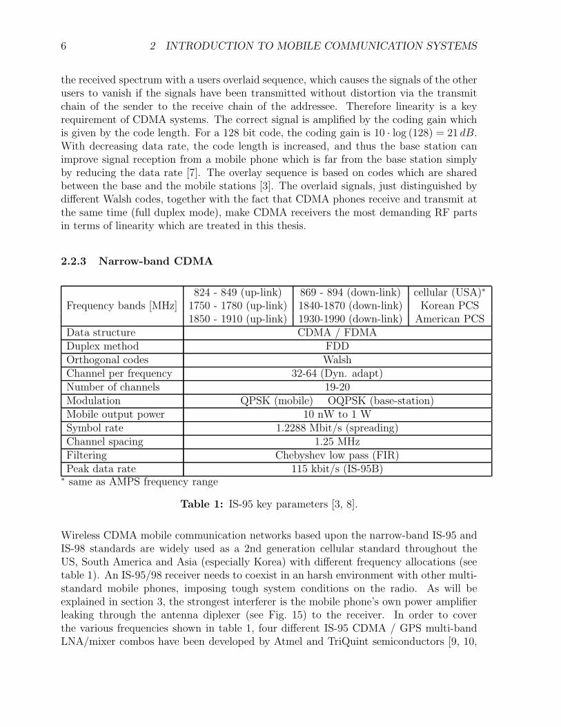
2.2.3 Narrow-band CDMA
824 - 849 (up-link) 869 - 894 (down-link) cellular (USA)∗
Frequency bands [MHz] 1750 - 1780 (up-link) 1840-1870 (down-link) Korean PCS1850 - 1910 (up-link) 1930-1990 (down-link) American PCS
Data structure CDMA / FDMADuplex method FDDOrthogonal codes WalshChannel per frequency 32-64 (Dyn. adapt)Number of channels 19-20Modulation QPSK (mobile) OQPSK (base-station)Mobile output power 10 nW to 1 WSymbol rate 1.2288 Mbit/s (spreading)Channel spacing 1.25 MHzFiltering Chebyshev low pass (FIR)Peak data rate 115 kbit/s (IS-95B)
∗ same as AMPS frequency range
Table 1: IS-95 key parameters [3, 8].
Wireless CDMA mobile communication networks based upon the narrow-band IS-95 andIS-98 standards are widely used as a 2nd generation cellular standard throughout theUS, South America and Asia (especially Korea) with different frequency allocations (seetable 1). An IS-95/98 receiver needs to coexist in an harsh environment with other multi-standard mobile phones, imposing tough system conditions on the radio. As will beexplained in section 3, the strongest interferer is the mobile phone’s own power amplifierleaking through the antenna diplexer (see Fig. 15) to the receiver. In order to coverthe various frequencies shown in table 1, four different IS-95 CDMA / GPS multi-bandLNA/mixer combos have been developed by Atmel and TriQuint semiconductors [9, 10,
2.2 Mobile phone standards 7
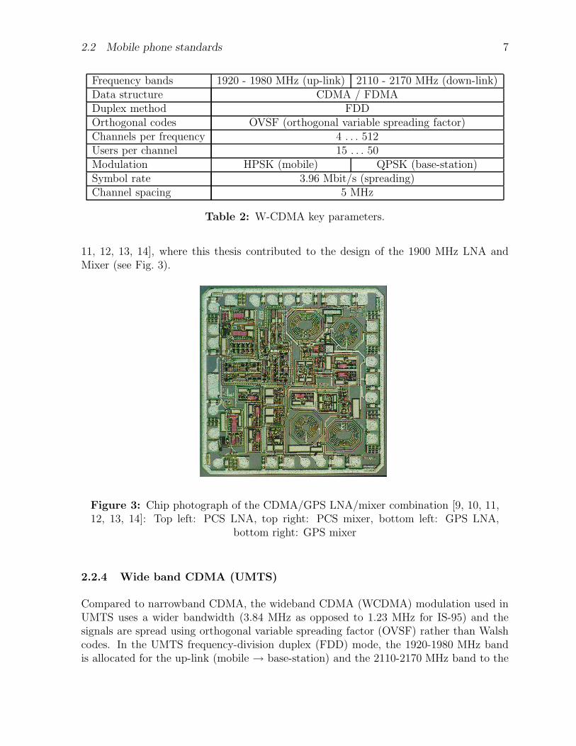
Frequency bands 1920 - 1980 MHz (up-link) 2110 - 2170 MHz (down-link)Data structure CDMA / FDMADuplex method FDDOrthogonal codes OVSF (orthogonal variable spreading factor)Channels per frequency 4 . . . 512Users per channel 15 . . . 50Modulation HPSK (mobile) QPSK (base-station)Symbol rate 3.96 Mbit/s (spreading)Channel spacing 5 MHz
Table 2: W-CDMA key parameters.
11, 12, 13, 14], where this thesis contributed to the design of the 1900 MHz LNA andMixer (see Fig. 3).
Figure 3: Chip photograph of the CDMA/GPS LNA/mixer combination [9, 10, 11,12, 13, 14]: Top left: PCS LNA, top right: PCS mixer, bottom left: GPS LNA,
bottom right: GPS mixer
2.2.4 Wide band CDMA (UMTS)
Compared to narrowband CDMA, the wideband CDMA (WCDMA) modulation used inUMTS uses a wider bandwidth (3.84 MHz as opposed to 1.23 MHz for IS-95) and thesignals are spread using orthogonal variable spreading factor (OVSF) rather than Walshcodes. In the UMTS frequency-division duplex (FDD) mode, the 1920-1980 MHz bandis allocated for the up-link (mobile → base-station) and the 2110-2170 MHz band to the
8 2 INTRODUCTION TO MOBILE COMMUNICATION SYSTEMS
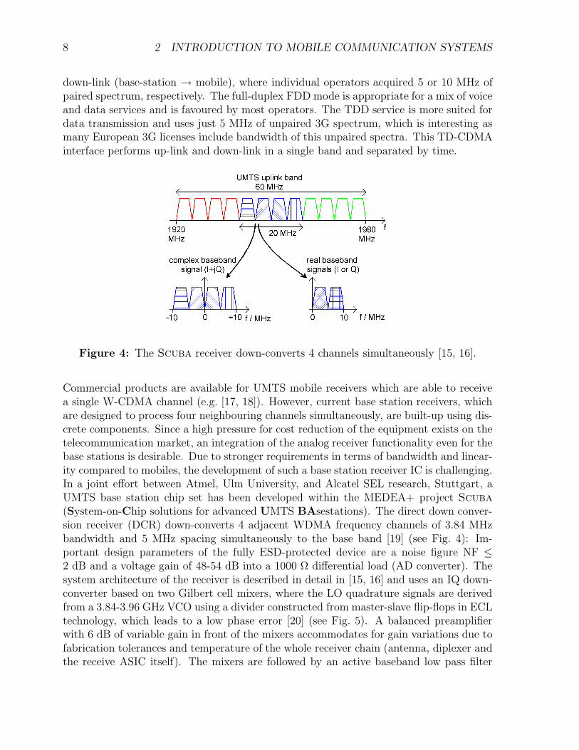
down-link (base-station → mobile), where individual operators acquired 5 or 10 MHz ofpaired spectrum, respectively. The full-duplex FDD mode is appropriate for a mix of voiceand data services and is favoured by most operators. The TDD service is more suited fordata transmission and uses just 5 MHz of unpaired 3G spectrum, which is interesting asmany European 3G licenses include bandwidth of this unpaired spectra. This TD-CDMAinterface performs up-link and down-link in a single band and separated by time.
Figure 4: The Scuba receiver down-converts 4 channels simultaneously [15, 16].
Commercial products are available for UMTS mobile receivers which are able to receivea single W-CDMA channel (e.g. [17, 18]). However, current base station receivers, whichare designed to process four neighbouring channels simultaneously, are built-up using dis-crete components. Since a high pressure for cost reduction of the equipment exists on thetelecommunication market, an integration of the analog receiver functionality even for thebase stations is desirable. Due to stronger requirements in terms of bandwidth and linear-ity compared to mobiles, the development of such a base station receiver IC is challenging.In a joint effort between Atmel, Ulm University, and Alcatel SEL research, Stuttgart, aUMTS base station chip set has been developed within the MEDEA+ project Scuba
(System-on-Chip solutions for advanced UMTS BAsestations). The direct down conver-sion receiver (DCR) down-converts 4 adjacent WDMA frequency channels of 3.84 MHzbandwidth and 5 MHz spacing simultaneously to the base band [19] (see Fig. 4): Im-portant design parameters of the fully ESD-protected device are a noise figure NF ≤2 dB and a voltage gain of 48-54 dB into a 1000 Ω differential load (AD converter). Thesystem architecture of the receiver is described in detail in [15, 16] and uses an IQ down-converter based on two Gilbert cell mixers, where the LO quadrature signals are derivedfrom a 3.84-3.96 GHz VCO using a divider constructed from master-slave flip-flops in ECLtechnology, which leads to a low phase error [20] (see Fig. 5). A balanced preamplifierwith 6 dB of variable gain in front of the mixers accommodates for gain variations due tofabrication tolerances and temperature of the whole receiver chain (antenna, diplexer andthe receive ASIC itself). The mixers are followed by an active baseband low pass filter
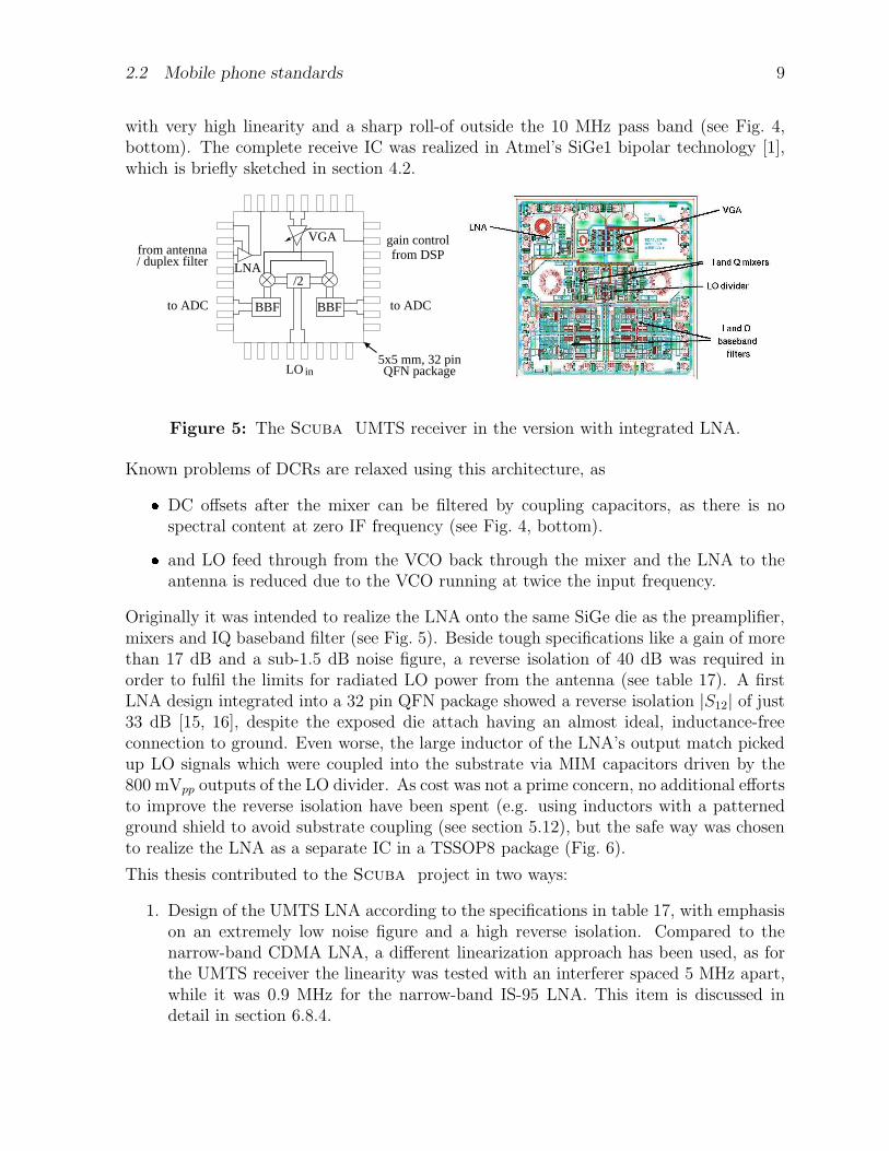
2.2 Mobile phone standards 9
with very high linearity and a sharp roll-of outside the 10 MHz pass band (see Fig. 4,bottom). The complete receive IC was realized in Atmel’s SiGe1 bipolar technology [1],which is briefly sketched in section 4.2.
LO in
from antenna/ duplex filter
5x5 mm, 32 pinQFN package
/2
VGA
to ADC
gain controlfrom DSP
LNA
to ADCBBF BBF
Figure 5: The Scuba UMTS receiver in the version with integrated LNA.
Known problems of DCRs are relaxed using this architecture, as DC offsets after the mixer can be filtered by coupling capacitors, as there is nospectral content at zero IF frequency (see Fig. 4, bottom). and LO feed through from the VCO back through the mixer and the LNA to theantenna is reduced due to the VCO running at twice the input frequency.
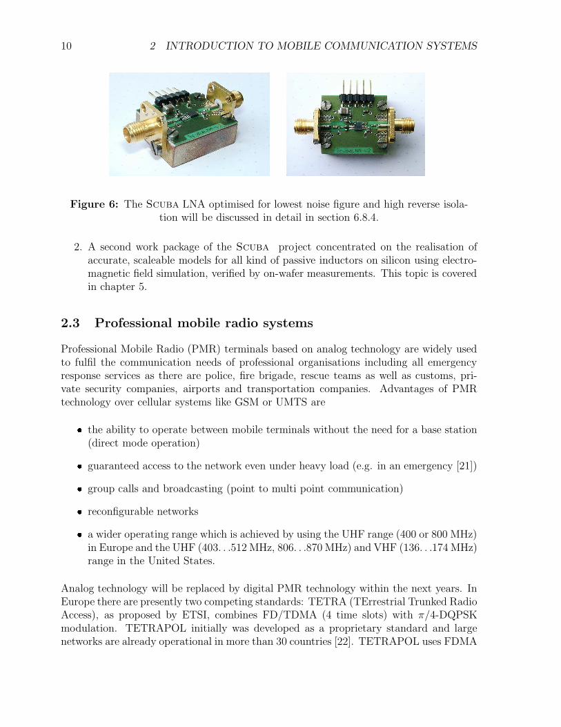
Originally it was intended to realize the LNA onto the same SiGe die as the preamplifier,mixers and IQ baseband filter (see Fig. 5). Beside tough specifications like a gain of morethan 17 dB and a sub-1.5 dB noise figure, a reverse isolation of 40 dB was required inorder to fulfil the limits for radiated LO power from the antenna (see table 17). A firstLNA design integrated into a 32 pin QFN package showed a reverse isolation |S12| of just33 dB [15, 16], despite the exposed die attach having an almost ideal, inductance-freeconnection to ground. Even worse, the large inductor of the LNA’s output match pickedup LO signals which were coupled into the substrate via MIM capacitors driven by the800 mVpp outputs of the LO divider. As cost was not a prime concern, no additional effortsto improve the reverse isolation have been spent (e.g. using inductors with a patternedground shield to avoid substrate coupling (see section 5.12), but the safe way was chosento realize the LNA as a separate IC in a TSSOP8 package (Fig. 6).
This thesis contributed to the Scuba project in two ways:
1. Design of the UMTS LNA according to the specifications in table 17, with emphasison an extremely low noise figure and a high reverse isolation. Compared to thenarrow-band CDMA LNA, a different linearization approach has been used, as forthe UMTS receiver the linearity was tested with an interferer spaced 5 MHz apart,while it was 0.9 MHz for the narrow-band IS-95 LNA. This item is discussed indetail in section 6.8.4.
10 2 INTRODUCTION TO MOBILE COMMUNICATION SYSTEMS
Figure 6: The Scuba LNA optimised for lowest noise figure and high reverse isola-tion will be discussed in detail in section 6.8.4.
2. A second work package of the Scuba project concentrated on the realisation ofaccurate, scaleable models for all kind of passive inductors on silicon using electro-magnetic field simulation, verified by on-wafer measurements. This topic is coveredin chapter 5.
2.3 Professional mobile radio systems
Professional Mobile Radio (PMR) terminals based on analog technology are widely usedto fulfil the communication needs of professional organisations including all emergencyresponse services as there are police, fire brigade, rescue teams as well as customs, pri-vate security companies, airports and transportation companies. Advantages of PMRtechnology over cellular systems like GSM or UMTS are the ability to operate between mobile terminals without the need for a base station
(direct mode operation) guaranteed access to the network even under heavy load (e.g. in an emergency [21]) group calls and broadcasting (point to multi point communication) reconfigurable networks a wider operating range which is achieved by using the UHF range (400 or 800 MHz)in Europe and the UHF (403. . .512 MHz, 806. . .870 MHz) and VHF (136. . .174 MHz)range in the United States.
Analog technology will be replaced by digital PMR technology within the next years. InEurope there are presently two competing standards: TETRA (TErrestrial Trunked RadioAccess), as proposed by ETSI, combines FD/TDMA (4 time slots) with π/4-DQPSKmodulation. TETRAPOL initially was developed as a proprietary standard and largenetworks are already operational in more than 30 countries [22]. TETRAPOL uses FDMA
2.4 Wireless Local Area Networks 11
source ETSI standard TETRAPOL forum TIA (U.S.A)www.tetramou.com www.tetrapol.com
multiple access FD / TDMA FDMA FDMAmodulation scheme π
4DQPSK GMSK C4FM (phase 1)
CQPSK (phase 2)channel spacing [kHz] 25 10 or 12.5 12.5 (phase 1)
6.25 (phase 2)frequency range UHF UHF VHF and UHF
Table 3: Overview of different standards for PMR terminals [23, 24, 25]
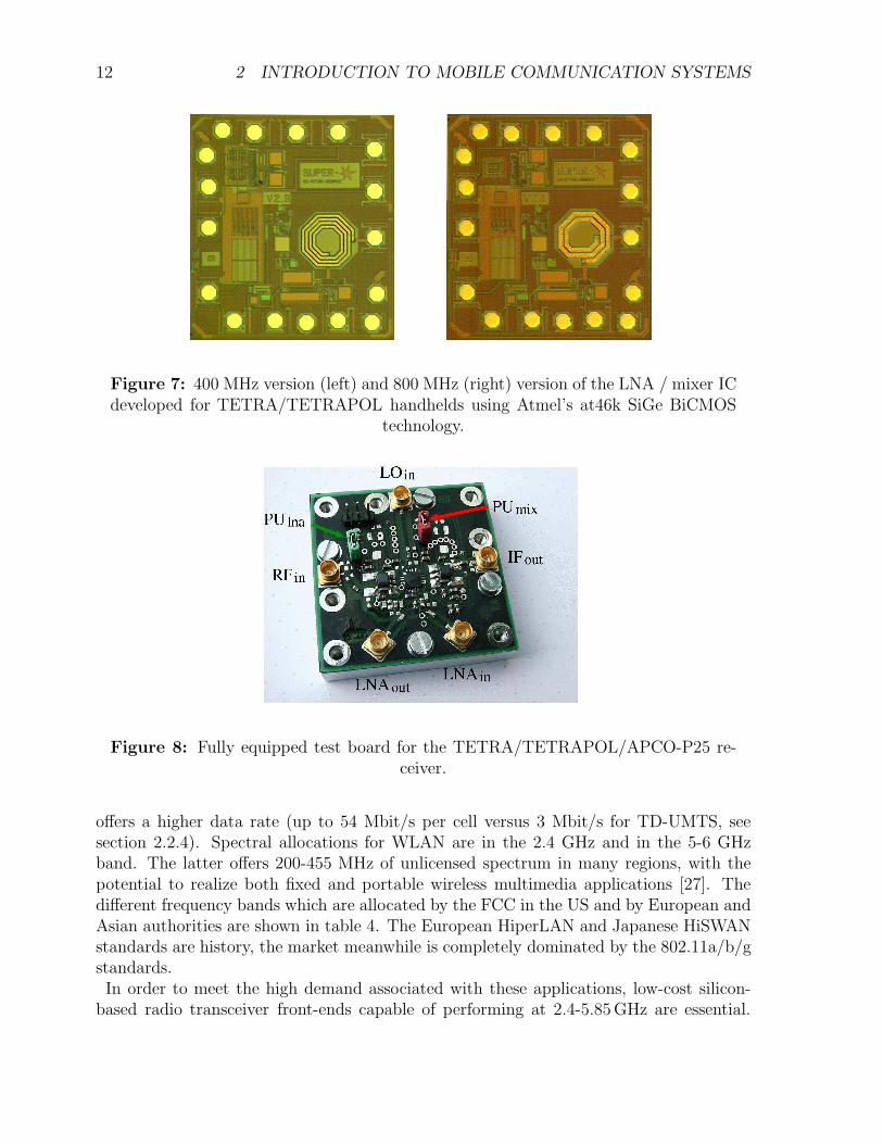
multiplexing and a robust GMSK modulation. Depending on the country, several bandsare allocated to PMR systems. They can be grouped into the 400 MHz bands (380-430 MHz, 440-490 MHz and 470-520 MHz) and a 800 MHz band (750-870 MHz). Withinthe MEDEA+ project SUPERSTAR (Silicon Universal Platform for Secured TelecomApplications), TETRA/TETRAPOL multi-mode terminals are developed which targetthe European market as well as the American market and therefore need to fulfil theAmerican APCO 25 standard as well. For APCO, analog Mutual Aid Channels (MACh)are required to allow inter-system communication with analog handhelds according tostandard TIA-603-B. However, none of the RF parameters is determined by these MACh’s.Inherent to all three standards is a low channel spacing of 6.25 . . . 25 kHz (see table 3).This requires both LNA and mixer to be robust against 3rd order intermodulation fromtwo very closely spaced tones due to co-location interference in rugged environments. Asinterferers appear in the receive band they cannot be reduced in amplitude by a SAW filterbetween LNA and mixer as it is the case in the IS-95, UMTS and GPS receiver developedduring this thesis. Therefore, special design techniques have been used to make (i) theLNA robust against interferers at small offset frequencies and (ii) to design a mixer withvery high linearity (see section 7.5.2) which considerably differs from the mixers designedfor CDMA and WLAN. The main differences between TETRA, TETRAPOL and APCOare summarised in table 3. The two receive ICs – one for the 400 MHz band and onefor the 750-870 MHz band – are shown Fig. 7 and will be discussed in detail in section 6and 7. Fig. 8 shows a fully equipped LNA/Mixer board using the IC shown in Fig. 7.
2.4 Wireless Local Area Networks
Wireless Local Area Networks (WLANs) are a low-cost alternative to cellular networksin providing data services at retailers, hotel chains, property owners, airports and trainstations to offer business travellers high-speed connectivity to their corporate networksas well as broadband internet access including voice-over-IP (VoIP) phone calls, withouthaving to invest into UMTS license fees [26]. Compared to cellular networks, WLAN
12 2 INTRODUCTION TO MOBILE COMMUNICATION SYSTEMS
Figure 7: 400 MHz version (left) and 800 MHz (right) version of the LNA / mixer ICdeveloped for TETRA/TETRAPOL handhelds using Atmel’s at46k SiGe BiCMOS
technology.
Figure 8: Fully equipped test board for the TETRA/TETRAPOL/APCO-P25 re-ceiver.
offers a higher data rate (up to 54 Mbit/s per cell versus 3 Mbit/s for TD-UMTS, seesection 2.2.4). Spectral allocations for WLAN are in the 2.4 GHz and in the 5-6 GHzband. The latter offers 200-455 MHz of unlicensed spectrum in many regions, with thepotential to realize both fixed and portable wireless multimedia applications [27]. Thedifferent frequency bands which are allocated by the FCC in the US and by European andAsian authorities are shown in table 4. The European HiperLAN and Japanese HiSWANstandards are history, the market meanwhile is completely dominated by the 802.11a/b/gstandards.In order to meet the high demand associated with these applications, low-cost silicon-
based radio transceiver front-ends capable of performing at 2.4-5.85GHz are essential.
2.4 Wireless Local Area Networks 13
standard country frequency maximum air access channelof origin range [GHz] data rate spacing
802.11b US 2.4 - 2.4835 11Mbps FHSS 1 MHzDSSS using CCK 25 MHz
802.11g US 2.4 - 2.4835 54Mbps OFDM using CCK 20 MHz
802.11a US 5.15 - 5.25 54Mbps OFDM 20 MHz(U-NII) 5.25 - 5.35
5.725- 5.825ISM bands 2.40 - 2.4835 Spread
5.725 - 5.85 spectrum
Table 4: Current WLAN standards [28, 29, 30]. Data for the ISM bands are forcomparison only.
Using Atmel’s SiGe-1 technology, a broadband image-reject (IR) mixer has been devel-oped within this thesis which achieves an image-rejection of more than 40 dB withoutthe need for any post-tuning (section 7.7). However, due to the low integration level,this receiver did not make it into a product. Pure 5GHz CMOS transceivers have beenreported with impressive RF performance [31, 32, 33, 34], albeit this comes at the ex-pense of a high power consumption [31]. While CMOS offers an advantage with respectto the integration level, the noise behaviour, current driveability and device matching isinferior compared to bipolar devices. In 2004, both BiCMOS and CMOS radios coexisted,
RFin
RFoutRFin
VCC
RFout
5 GHz
100pF
PU24
PU5
2.4 GHz
2.4 GHz
5 GHz
100pF
1nF
100pF27pF
54pF
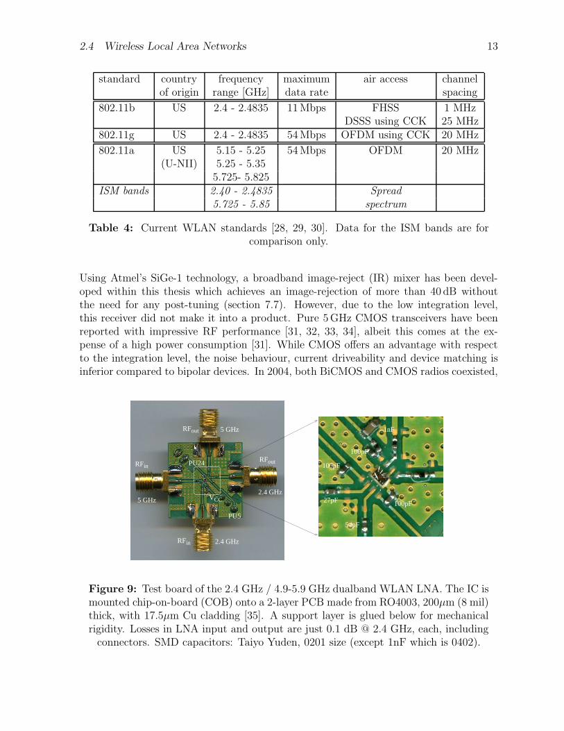
Figure 9: Test board of the 2.4 GHz / 4.9-5.9 GHz dualband WLAN LNA. The IC ismounted chip-on-board (COB) onto a 2-layer PCB made from RO4003, 200µm (8 mil)thick, with 17.5µm Cu cladding [35]. A support layer is glued below for mechanicalrigidity. Losses in LNA input and output are just 0.1 dB @ 2.4 GHz, each, including
connectors. SMD capacitors: Taiyo Yuden, 0201 size (except 1nF which is 0402).
14 2 INTRODUCTION TO MOBILE COMMUNICATION SYSTEMS
where SiGe BiCMOS offers 5 dB higher sensitivity compared to CMOS [36]. Due to theenormous price pressure and the trend towards very high integration levels, CMOS radiosusing direct conversion architectures (DCR) will inevitably win the race. Opportunitiesfor SiGe remain, but only in the front-end section (power amplifier or low noise amplifier).To date most CMOS radios offer reasonable noise performance at 2.4 GHz, but 5 GHzperformance is still poor with receiver (RX) noise figures around 5-6 dB [32, 34]. There-fore, at the end of this thesis, a 4.9-5.9 GHz LNA has been developed according to thespecifications of a European manufacturer of front-end modules [37]. These modules arefabricated using low-temperature co-fired ceramic (LTCC) and integrate a T/R switch(usually GaAs pHEMT), band pass filters for receiver (RX) and transmitter (TX), andsometimes a power amplifier [38]. This PA is usually built with InGaP HBTs [39, 40] orGaAs pHEMTs [41], as SiGe HBTs optimised for large breakdown voltages lack sufficientgain at high frequencies (see table 26). Interfaces to the radio are either single-ended orbalanced, the latter being electrically superior but requiring additional signal lines. Whilesome of the front-end modules on the market do not contain active parts in the RX pathand show a transmission loss of ≈3 dB [42], the 802.11a standard benefits from a lownoise preamplifier within the module. Modules with integrated LNA are on the marketand use GaAs pHEMT technology for both switch and LNA [43, 38]. The LTCC processallows passive components such as resistors, inductors and capacitors with high qualityfactors3 to be embedded in a multilayer, integrated module with high density and lowcost [44, 38]. It turned out, however, that larger values of capacitors (>500 fF) and in-ductors consume large area on the LTCC and require the use of SMD components placedon the top of the module, which is unwanted. Finally, to keep prices low, all passivesof the LNA were realised on silicon, except the input blocking capacitor, which - whenintegrated on Si - would increase the noise figure by more than 0.5 dB at 2.4 GHz (ADSsimulation). The LNA results are presented in section 6.8.9. A balanced architecture, asit was published by our group earlier [45], is easier to package due to a virtual ground atthe symmetry point and offers a better signal integrity. However, as the antenna interfaceis always single-ended, a single ended LNA design was chosen here. The output can thenbe converted to a balanced signal by a balun on the module. In addition, the use ofSiGe2-Power for the single-ended design offers much better noise performance than thebalanced LNA using SiGe1. Later on, a 2.4 GHz LNA for 802.11b/g systems was addedto the 5 GHz LNA (see Fig. 9).
2.5 Global Positioning Systems
The Global Positioning System [46] has been launched by the US for military navigationpurposes. It is a satellite-based location/time finding system with 24 satellites (plusreserve satellites) orbiting the earth. They are located in 6 orbital planes in an altitudeof 20180 km with an inclination of 55. The satellites, which have a period of revolutionof 11h58m00s, transmit signals in both the L1 band (1575.42 MHz) and the L2 band
3The quality factor is defined in detail in section 5.6.
2.5 Global Positioning Systems 15
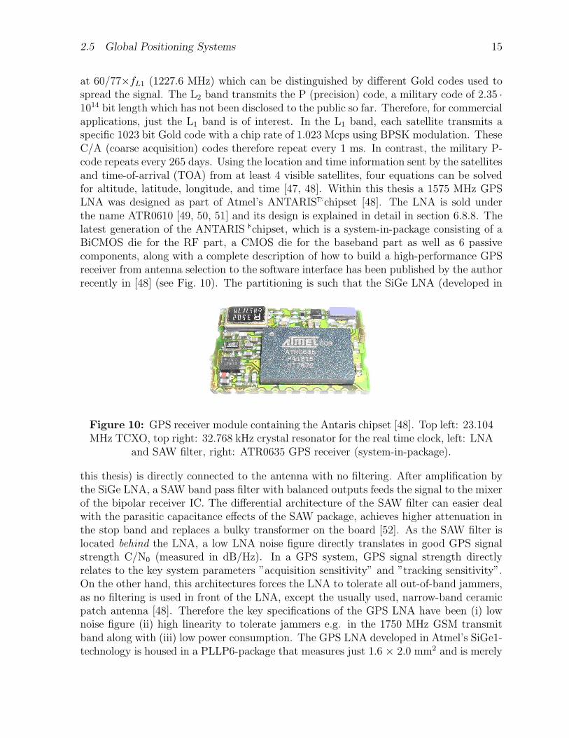
at 60/77×fL1 (1227.6 MHz) which can be distinguished by different Gold codes used tospread the signal. The L2 band transmits the P (precision) code, a military code of 2.35 ·1014 bit length which has not been disclosed to the public so far. Therefore, for commercialapplications, just the L1 band is of interest. In the L1 band, each satellite transmits aspecific 1023 bit Gold code with a chip rate of 1.023 Mcps using BPSK modulation. TheseC/A (coarse acquisition) codes therefore repeat every 1 ms. In contrast, the military P-code repeats every 265 days. Using the location and time information sent by the satellitesand time-of-arrival (TOA) from at least 4 visible satellites, four equations can be solvedfor altitude, latitude, longitude, and time [47, 48]. Within this thesis a 1575 MHz GPSLNA was designed as part of Atmel’s ANTARISchipset [48]. The LNA is sold underthe name ATR0610 [49, 50, 51] and its design is explained in detail in section 6.8.8. Thelatest generation of the ANTARISchipset, which is a system-in-package consisting of aBiCMOS die for the RF part, a CMOS die for the baseband part as well as 6 passivecomponents, along with a complete description of how to build a high-performance GPSreceiver from antenna selection to the software interface has been published by the authorrecently in [48] (see Fig. 10). The partitioning is such that the SiGe LNA (developed in
Figure 10: GPS receiver module containing the Antaris chipset [48]. Top left: 23.104MHz TCXO, top right: 32.768 kHz crystal resonator for the real time clock, left: LNA
and SAW filter, right: ATR0635 GPS receiver (system-in-package).
this thesis) is directly connected to the antenna with no filtering. After amplification bythe SiGe LNA, a SAW band pass filter with balanced outputs feeds the signal to the mixerof the bipolar receiver IC. The differential architecture of the SAW filter can easier dealwith the parasitic capacitance effects of the SAW package, achieves higher attenuation inthe stop band and replaces a bulky transformer on the board [52]. As the SAW filter islocated behind the LNA, a low LNA noise figure directly translates in good GPS signalstrength C/N0 (measured in dB/Hz). In a GPS system, GPS signal strength directlyrelates to the key system parameters ”acquisition sensitivity” and ”tracking sensitivity”.On the other hand, this architectures forces the LNA to tolerate all out-of-band jammers,as no filtering is used in front of the LNA, except the usually used, narrow-band ceramicpatch antenna [48]. Therefore the key specifications of the GPS LNA have been (i) lownoise figure (ii) high linearity to tolerate jammers e.g. in the 1750 MHz GSM transmitband along with (iii) low power consumption. The GPS LNA developed in Atmel’s SiGe1-technology is housed in a PLLP6-package that measures just 1.6 × 2.0 mm2 and is merely
16 3 SYSTEM CONSIDERATIONS AND LEVEL PLANNING
GPS Galileo
# of satellites (reserve) 24 (6) 27 (3)altitude 20180 km 23616 km (MEO)equatorial inclination 55 56
frequency bands 1575.42 MHz (L1) 1561-1590 MHz (L1)1227.60 MHz (L2) 1176-1207 MHz (E5a, E5b)
1269-1289 MHz (E6)modulation BPSK Binary Offset Carrier (BOC)chip rate 1.023 Mcps (CA code) 1.023 Mcpsspeed 50 bit/s (CA code) 250 symbols/spilot channel no yes (BPSK modulated)code Gold (1023) Gold (8184-10230)power 5-6 dB above GPS level
Table 5: Key parameters of the American GPS and the European Galileo system [46,55, 56].
bigger than the size of a discrete transistor (see section 6.8.8). This small size and its fullESD protection make it an ideal candidate for active GPS antennas.When the European Galileo system will go into operation somewhere in 2013 [53], thecombined correlation of GPS and Galileo satellites shall give an availability of positioninformation in 95% of all cases together with an improved location accuracy. Galileois a Global Navigation Satellite System (GNSS) initiated by the European Commissionand the European Space Agency (ESA) and compatible with but independent from theAmerican Global Positioning System (GPS). The main differences between GPS andGalileo are sketched in table 5. Compared to a GPS receiver, for optimum performancea Galileo receiver will need a broadband front-end with a flexible frequency plan to coverall 4 bands. The standard consumer receiver, however, will just receive the free Galileoservice in the L1 band [54]. Due to its broadband nature, the GPS SiGe LNA developedin this thesis can be used to receive the important Galileo L1-band as well.
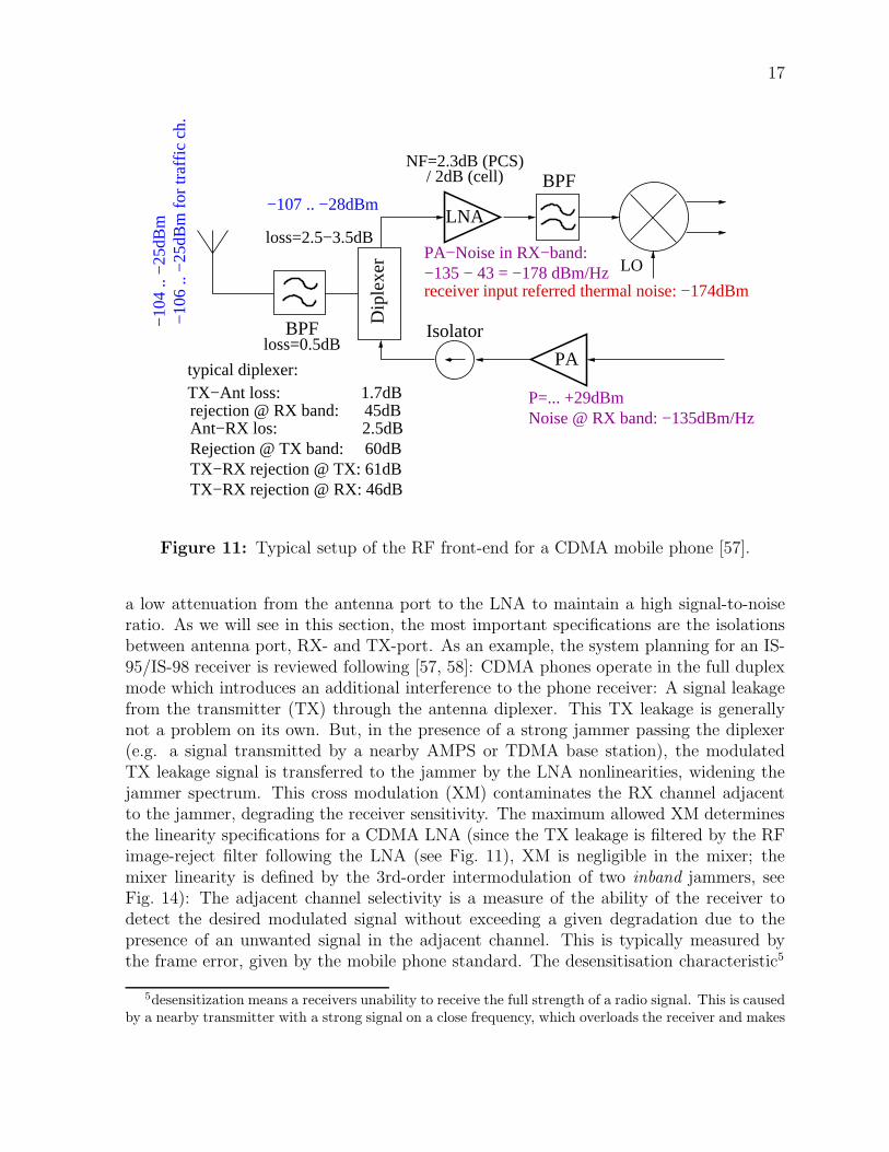
3 System considerations and level planning
A typical setup of a CDMA phone is shown in Fig. 114: Connected to the antenna is aband pass filter which blocks signals below the TX-band and above the RX-band. Dueto the full duplex mode of a CDMA phone, the diplexer (see Fig. 15), the equivalent ofthe antenna switch of a TDMA phone, is a very important part: It needs to have a lowattenuation from the PA to the antenna in order to guarantee a good PA efficiency and
4The isolator following the PA is often omitted in modern phones in order to improve power addedefficiency (PAE) of the transmitter and save cost as well as PCB real estate. This, however, requires thePA to withstand VSWR-ratios of higher than 10:1 without damage.
17
Dip
lexe
r
LNA
PA
BPF
−107 .. −28dBm
LO
receiver input referred thermal noise: −174dBm
P=... +29dBm
BPF−
106
.. −
25dB
m fo
r tr
affic
ch.
−10
4 ..
−25
dBm
loss=0.5dB
loss=2.5−3.5dB
NF=2.3dB (PCS)/ 2dB (cell)
typical diplexer:TX−Ant loss: 1.7dB
Noise @ RX band: −135dBm/Hzrejection @ RX band: 45dBAnt−RX los: 2.5dB
TX−RX rejection @ RX: 46dBTX−RX rejection @ TX: 61dBRejection @ TX band: 60dB
Isolator
−135 − 43 = −178 dBm/HzPA−Noise in RX−band:
Figure 11: Typical setup of the RF front-end for a CDMA mobile phone [57].
a low attenuation from the antenna port to the LNA to maintain a high signal-to-noiseratio. As we will see in this section, the most important specifications are the isolationsbetween antenna port, RX- and TX-port. As an example, the system planning for an IS-95/IS-98 receiver is reviewed following [57, 58]: CDMA phones operate in the full duplexmode which introduces an additional interference to the phone receiver: A signal leakagefrom the transmitter (TX) through the antenna diplexer. This TX leakage is generallynot a problem on its own. But, in the presence of a strong jammer passing the diplexer(e.g. a signal transmitted by a nearby AMPS or TDMA base station), the modulatedTX leakage signal is transferred to the jammer by the LNA nonlinearities, widening thejammer spectrum. This cross modulation (XM) contaminates the RX channel adjacentto the jammer, degrading the receiver sensitivity. The maximum allowed XM determinesthe linearity specifications for a CDMA LNA (since the TX leakage is filtered by the RFimage-reject filter following the LNA (see Fig. 11), XM is negligible in the mixer; themixer linearity is defined by the 3rd-order intermodulation of two inband jammers, seeFig. 14): The adjacent channel selectivity is a measure of the ability of the receiver todetect the desired modulated signal without exceeding a given degradation due to thepresence of an unwanted signal in the adjacent channel. This is typically measured bythe frame error, given by the mobile phone standard. The desensitisation characteristic5
5desensitization means a receivers unability to receive the full strength of a radio signal. This is causedby a nearby transmitter with a strong signal on a close frequency, which overloads the receiver and makes

18 3 SYSTEM CONSIDERATIONS AND LEVEL PLANNING
of the receiver determines its ability to operate successfully under strong interferers. Thisrequires an LNA with exceptional high linearity that should be achieved
1. without degrading the LNA NF and gain since the desired RX signal from a basestation at maximum distance to the mobile phone is very weak, while the mobilephone in this condition transmits at its maximum output power. This is because theCDMA mobile phone sets its output power according to PTX [dBm] = −73−PRX inthe cellular band and PTX [dBm] = −76 − PRX in the PCS band [60], so minimumRX power always translates into maximum TX power. In addition, the signal maybe jammed by a nearby AMPS or TDMA base station.
2. with a low power consumption to extend the talk time of the phone, and
3. with a low-cost technology allowing a high level of integration.
While previously GaAs MESFET front-ends containing LNA and mixer have been used,the industry meanwhile has switched to SiGe transceivers [58, 61], with RF CMOS solu-tions being in the pipeline [62].
3.1 Intermodulation distortion
IM3
f1− f2 f2 f1 − f22f1− f12f2frequency
output power [dBm]
Figure 12: Applying two tones to a nonlinear device leads to intermodulation dis-tortion.
Intermodulation distortion is the result of two or more signals interacting in a nonlineardevice to produce additional unwanted signals [63]. These additional signals (intermodula-tion products) occur mainly in devices such as amplifiers and mixers, but to a lesser extent
it unable to fully receive the desired signal [59].
3.1 Intermodulation distortion 19
they also occur in passive devices such as ceramic SMD capacitors with a low voltage co-efficient (capacitance slightly varying with applied RF voltage swing), parts containingmagnetic materials such as circulators and isolators and corroded RF connectors [63].This thesis concentrates on the reduction of intermodulation products in Low Noise Am-plifiers (LNAs) and mixers. As can be found in numerous textbooks (e.g. [64, 65]) andscripts [66], the non-ideal characteristics of a weakly non-linear amplifier can be describedby using the power series expansion:
Vout = K0 + K1 × Vin + K2 × V 2in + K3 × V 3
in + . . . (1)
Applying a one-tone excitation Vin = E ·sin (ω · t) and using sin (3a) = 3·sin (a)−4·sin3 (a)and cos (2a) = 1 − 2 · sin2 (a) results in
Vout =
[
K0 +K2 · E2
2
]
+
[
K1 · E +3 · K3 · E3
4
]
× sin (ω · t) (2)
− K2 · E2
2× cos (2 · ω · t) +
K3 · E3
4× sin (3 · ω · t) (3)
This shows that a one-tone input signal produces harmonic distortion (Eqn. 3), as wellas DC offset and gain compression (Eqn. 2, K3 < 0). A two-tone input signal
Vin = E1 · sin (ω1 · t) + E2 · sin (ω2 · t) (4)
produces harmonic distortion and intermodulation distortion: Combining Eqns. 1 and 4results in
Vout = K0 + K1 · E1 · sin (ω1 · t) + E2 · sin (ω2 · t)+ K2 · E1 · sin (ω1 · t) + E2 · sin (ω2 · t)2 (5)
+ K3 · E1 · sin (ω1 · t) + E2 · sin (ω2 · t)3 + . . .
The first term K0 represents the DC offset of the amplifier, the second term is the fun-damental signal. The subsequent terms represent the distortion of the amplifier. The2nd order intermodulation distortion (IMD) can be found by analysing the third term ofEqn. 5 by using the identities above and sin (a) · sin (b) = cos (a − b) − cos (a + b)/2
K2(vin)2 = K2 · E21 · sin2 (ω1 · t) + E2
2 · sin2 (ω2 · t) + 2 · E1 · E2 · sin (ω1 · t) · sin (ω2 · t)
= K2E2
1 + E22
2− K2
2
[
E21 · cos (2 · ω1 · t) + E2
2 · cos (2 · ω2 · t)]
(6)
+K2 · E1 · E2 [cos (ω1 · t − ω2 · t) − cos (ω1 · t + ω2 · t)]
The first and second terms in Eqn. 6 represent DC offset and second-order harmonics.The third term is the second order IMD. This exercise can be repeated with the fourth
20 3 SYSTEM CONSIDERATIONS AND LEVEL PLANNING
term of Eqn. 5 to study third-order effects.
K3(vin)3 = K3E31 · sin3 (ω1 · t) + E3
2 · sin3 (ω2 · t) (7)
+ 3 · E21 · E2 · sin2 (ω1 · t) · sin (ω2 · t) + 3 · E1 · E2
2 · sin (ω1 · t) · sin2 (ω2 · t)
By using sin3 (a) = 1/4[3 sin (a)−sin (3a)] and sin2 (a)·sin (b) = 1/2[sin (b)−1/2 sin (2a + b)−sin (2a − b)] this gives
K3(vin)3 =3 · K3
4E3
1 · sin (ω1 · t) + E32 · sin (ω2 · t)
+ 2 · E21 · E2 · sin (ω2 · t) + 2 · E1 · E2
2 · sin (ω1 · t) (8)
− K3
4E3
1 · sin (3ω1 · t) + E32 · sin (3ω2 · t) (9)
− 3 · K3 · E21 · E2
2sin (2ω1 · t − ω2 · t) −
1
2sin (2ω1 · t + ω2 · t) (10)
− 3 · K3 · E1 · E22
2sin (2ω2 · t − ω1 · t) −
1
2sin (2ω2 · t + ω1 · t) (11)
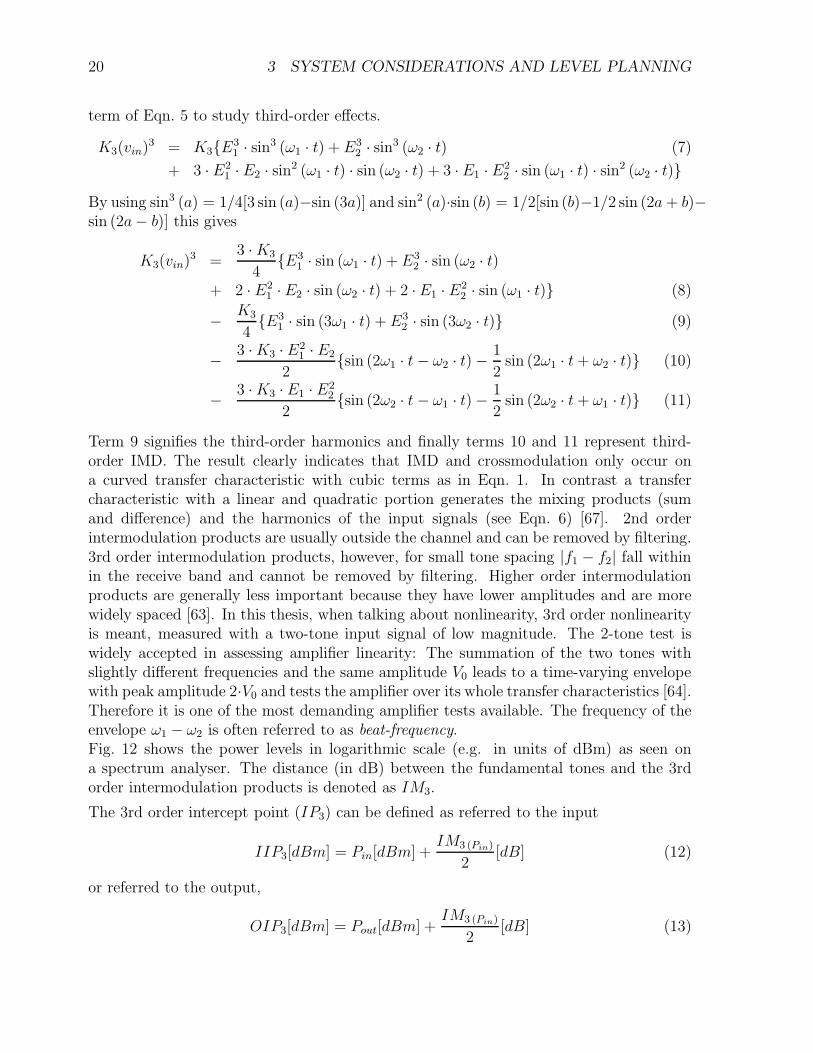
Term 9 signifies the third-order harmonics and finally terms 10 and 11 represent third-order IMD. The result clearly indicates that IMD and crossmodulation only occur ona curved transfer characteristic with cubic terms as in Eqn. 1. In contrast a transfercharacteristic with a linear and quadratic portion generates the mixing products (sumand difference) and the harmonics of the input signals (see Eqn. 6) [67]. 2nd orderintermodulation products are usually outside the channel and can be removed by filtering.3rd order intermodulation products, however, for small tone spacing |f1 − f2| fall withinin the receive band and cannot be removed by filtering. Higher order intermodulationproducts are generally less important because they have lower amplitudes and are morewidely spaced [63]. In this thesis, when talking about nonlinearity, 3rd order nonlinearityis meant, measured with a two-tone input signal of low magnitude. The 2-tone test iswidely accepted in assessing amplifier linearity: The summation of the two tones withslightly different frequencies and the same amplitude V0 leads to a time-varying envelopewith peak amplitude 2·V0 and tests the amplifier over its whole transfer characteristics [64].Therefore it is one of the most demanding amplifier tests available. The frequency of theenvelope ω1 − ω2 is often referred to as beat-frequency.Fig. 12 shows the power levels in logarithmic scale (e.g. in units of dBm) as seen ona spectrum analyser. The distance (in dB) between the fundamental tones and the 3rdorder intermodulation products is denoted as IM3.
The 3rd order intercept point (IP3) can be defined as referred to the input
IIP3[dBm] = Pin[dBm] +IM3 (Pin)
2[dB] (12)
or referred to the output,
OIP3[dBm] = Pout[dBm] +IM3 (Pin)
2[dB] (13)
3.1 Intermodulation distortion 21
1dB
outp
ut le
vel [
dBm
]
OIP3
input level [dBm]
IM3
1dB compression point(output referred)
SOI(second order
intercept point)
TOI(third order
intercept point)
P1dB
3IIP
Figure 13: Definition of 1dB-compression and 2nd and 3rd order intercept point.
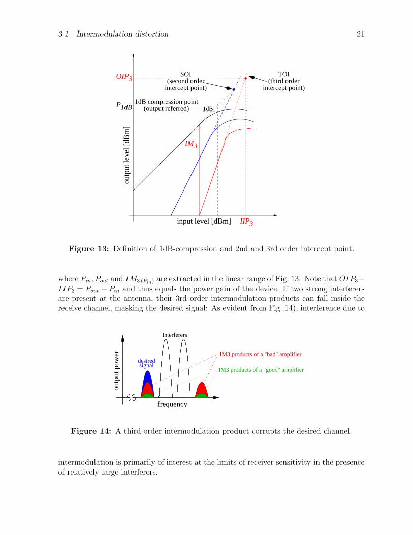
where Pin, Pout and IM3 (Pin) are extracted in the linear range of Fig. 13. Note that OIP3−IIP3 = Pout − Pin and thus equals the power gain of the device. If two strong interferersare present at the antenna, their 3rd order intermodulation products can fall inside thereceive channel, masking the desired signal: As evident from Fig. 14), interference due to
outp
ut p
ower
Interferers
desiredsignal
frequency
IM3 products of a "bad" amplifier
IM3 products of a "good" amplifier
Figure 14: A third-order intermodulation product corrupts the desired channel.
intermodulation is primarily of interest at the limits of receiver sensitivity in the presenceof relatively large interferers.
22 3 SYSTEM CONSIDERATIONS AND LEVEL PLANNING
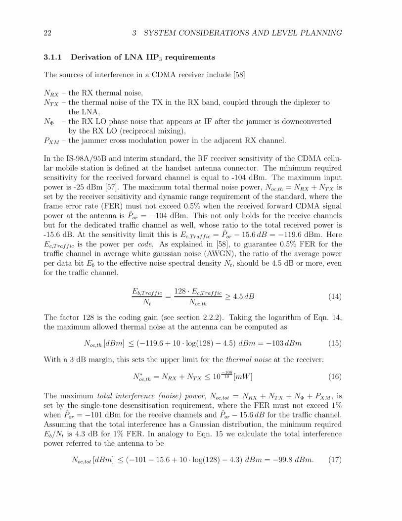
3.1.1 Derivation of LNA IIP3 requirements
The sources of interference in a CDMA receiver include [58]
NRX – the RX thermal noise,NTX – the thermal noise of the TX in the RX band, coupled through the diplexer to
the LNA,NΦ – the RX LO phase noise that appears at IF after the jammer is downconverted
by the RX LO (reciprocal mixing),PXM – the jammer cross modulation power in the adjacent RX channel.
In the IS-98A/95B and interim standard, the RF receiver sensitivity of the CDMA cellu-lar mobile station is defined at the handset antenna connector. The minimum requiredsensitivity for the received forward channel is equal to -104 dBm. The maximum inputpower is -25 dBm [57]. The maximum total thermal noise power, Noc,th = NRX + NTX isset by the receiver sensitivity and dynamic range requirement of the standard, where theframe error rate (FER) must not exceed 0.5% when the received forward CDMA signalpower at the antenna is Por = −104 dBm. This not only holds for the receive channelsbut for the dedicated traffic channel as well, whose ratio to the total received power is-15.6 dB. At the sensitivity limit this is Ec,T raffic = Por − 15.6 dB = −119.6 dBm. HereEc,T raffic is the power per code. As explained in [58], to guarantee 0.5% FER for thetraffic channel in average white gaussian noise (AWGN), the ratio of the average powerper data bit Eb to the effective noise spectral density Nt, should be 4.5 dB or more, evenfor the traffic channel.
Eb,T raffic
Nt=
128 · Ec,T raffic
Noc,th≥ 4.5 dB (14)
The factor 128 is the coding gain (see section 2.2.2). Taking the logarithm of Eqn. 14,the maximum allowed thermal noise at the antenna can be computed as
Noc,th [dBm] ≤ (−119.6 + 10 · log(128) − 4.5) dBm = −103 dBm (15)
With a 3 dB margin, this sets the upper limit for the thermal noise at the receiver:
N∗oc,th = NRX + NTX ≤ 10
−10610 [mW ] (16)
The maximum total interference (noise) power, Noc,tot = NRX + NTX + NΦ + PXM , isset by the single-tone desensitisation requirement, where the FER must not exceed 1%when Por = −101 dBm for the receive channels and Por − 15.6 dB for the traffic channel.Assuming that the total interference has a Gaussian distribution, the minimum requiredEb/Nt is 4.3 dB for 1% FER. In analogy to Eqn. 15 we calculate the total interferencepower referred to the antenna to be
Noc,tot [dBm] ≤ (−101 − 15.6 + 10 · log(128) − 4.3) dBm = −99.8 dBm. (17)
3.1 Intermodulation distortion 23
The noise margin for reciprocal mixing and jammer cross modulation is therefore limitedto
10−10610 + NΦ + PXM ≤ 10
−99.810 [mW ] (18)
For the single-tone desensitisation test case, the jammer is ν0 = 900 kHz away fromthe centre of the RX channel center. So, the RX LO phase noise that appears in theRX channel due to the reciprocal mixing is confined to a 900 kHz ± 1.23 MHz/2 =285. . .1515 kHz frequency-offset range. As this is outside of the PLL loop filter bandwidth,we consider the noise of a free running VCO here which is proportional to 1/ν2 with respectto the carrier in the above mentioned frequency range. Optimised, discrete CDMA VCOsshow typical values of Φ0 = −133.5 dBc/Hz at ν0 = 900 kHz offset from the carrier [68].
Φ(ν) =Φ0 · ν2
0
ν2(19)
Integrating this 1/ν2 noise shape over the 285. . .1515 kHz frequency range gives
ηΦ =∫ ν2
ν1
Φ0 · ν20
ν2dν = Φ0 · ν2
0 · −1
ν2
+1
ν1
(20)
= 10−13.35 mW/Hz · (900 kHz)2 · − 1
1515 kHz+
1
285 kHz = −69.9 dBc (21)
Taking into account a 3 dB improvement in phase noise due to the LO frequency dividerwhich is often used, yields -72.9 dBc. Referencing this phase noise to the PJ = -30 dBmjammer power at the antenna, we get for the receiver’s LO phase noise contributionNΦ = −102.9 dBm. According to Eqn. 18, this leaves a maximum of PXM ≤ −105.5 dBmfor the cross modulation contribution due to the -30 dBm jammer. Finally, using [58] andEqn. 12, this cross modulation power is related to the LNA linearity by
PXM [dBm] = PJ + 2
PTX + LTX − LTX−RX︸ ︷︷ ︸
TX power as seen on LNA input
− 2 · IIP3 − 2.4 (22)
where PTX = 23 dBm is the maximum transmit output power at the antenna, LTX is thediplexer TX-antenna insertion loss and LTX−RX is the diplexer’s TX-RX isolation (fromthe PA to the LNA input) in the TX band. The correction factor ”2.4 dB” takes intoaccount that the CDMA signal is not a continuous single tone, as assumed in Eqn. 12.Note that both Eqns. 12 and 22 are valid only in dBm! Rearranging Eqn. 22 results in thefollowing relationship between the diplexer characteristics and the LNA minimum IIP3,satisfying the single-tone desensitisation requirement:
IIP3,min[dBm] = PJ/2+PTX+LTX−LTX−RX−PXM/2−1.2 = 59.5−LTX−RX+LTX (23)
From Eqn. 23 it is evident that the diplexer is a key part in a CDMA phone and itsperformance translates directly into the linearity requirements of the front-end: Assuminga TX-RX isolation of 53 dB and a TX loss of 2.7 dB, the required minimum IIP3 is
24 3 SYSTEM CONSIDERATIONS AND LEVEL PLANNING
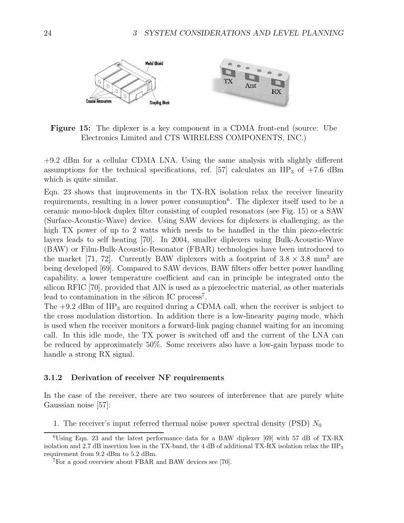
Figure 15: The diplexer is a key component in a CDMA front-end (source: UbeElectronics Limited and CTS WIRELESS COMPONENTS, INC.)
+9.2 dBm for a cellular CDMA LNA. Using the same analysis with slightly differentassumptions for the technical specifications, ref. [57] calculates an IIP3 of +7.6 dBmwhich is quite similar.
Eqn. 23 shows that improvements in the TX-RX isolation relax the receiver linearityrequirements, resulting in a lower power consumption6. The diplexer itself used to be aceramic mono-block duplex filter consisting of coupled resonators (see Fig. 15) or a SAW(Surface-Acoustic-Wave) device. Using SAW devices for diplexers is challenging, as thehigh TX power of up to 2 watts which needs to be handled in the thin piezo-electriclayers leads to self heating [70]. In 2004, smaller diplexers using Bulk-Acoustic-Wave(BAW) or Film-Bulk-Acoustic-Resonator (FBAR) technologies have been introduced tothe market [71, 72]. Currently BAW diplexers with a footprint of 3.8 × 3.8 mm2 arebeing developed [69]. Compared to SAW devices, BAW filters offer better power handlingcapability, a lower temperature coefficient and can in principle be integrated onto thesilicon RFIC [70], provided that AlN is used as a piezoelectric material, as other materialslead to contamination in the silicon IC process7.The +9.2 dBm of IIP3 are required during a CDMA call, when the receiver is subject tothe cross modulation distortion. In addition there is a low-linearity paging mode, whichis used when the receiver monitors a forward-link paging channel waiting for an incomingcall. In this idle mode, the TX power is switched off and the current of the LNA canbe reduced by approximately 50%. Some receivers also have a low-gain bypass mode tohandle a strong RX signal.
3.1.2 Derivation of receiver NF requirements
In the case of the receiver, there are two sources of interference that are purely whiteGaussian noise [57]:
1. The receiver’s input referred thermal noise power spectral density (PSD) N0
6Using Eqn. 23 and the latest performance data for a BAW diplexer [69] with 57 dB of TX-RXisolation and 2.7 dB insertion loss in the TX-band, the 4 dB of additional TX-RX isolation relax the IIP3
requirement from 9.2 dBm to 5.2 dBm.7For a good overview about FBAR and BAW devices see [70].
3.1 Intermodulation distortion 25
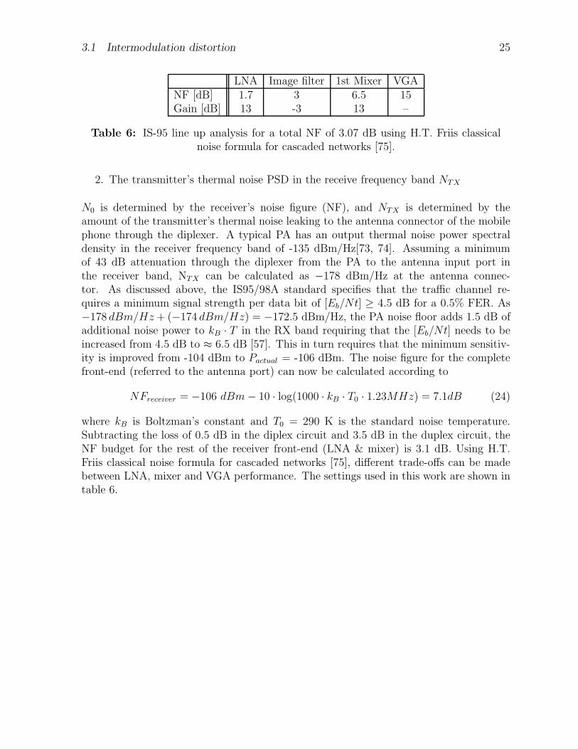
LNA Image filter 1st Mixer VGANF [dB] 1.7 3 6.5 15Gain [dB] 13 -3 13 –
Table 6: IS-95 line up analysis for a total NF of 3.07 dB using H.T. Friis classicalnoise formula for cascaded networks [75].
2. The transmitter’s thermal noise PSD in the receive frequency band NTX
N0 is determined by the receiver’s noise figure (NF), and NTX is determined by theamount of the transmitter’s thermal noise leaking to the antenna connector of the mobilephone through the diplexer. A typical PA has an output thermal noise power spectraldensity in the receiver frequency band of -135 dBm/Hz[73, 74]. Assuming a minimumof 43 dB attenuation through the diplexer from the PA to the antenna input port inthe receiver band, NTX can be calculated as −178 dBm/Hz at the antenna connec-tor. As discussed above, the IS95/98A standard specifies that the traffic channel re-quires a minimum signal strength per data bit of [Eb/Nt] ≥ 4.5 dB for a 0.5% FER. As−178 dBm/Hz + (−174 dBm/Hz) = −172.5 dBm/Hz, the PA noise floor adds 1.5 dB ofadditional noise power to kB · T in the RX band requiring that the [Eb/Nt] needs to beincreased from 4.5 dB to ≈ 6.5 dB [57]. This in turn requires that the minimum sensitiv-ity is improved from -104 dBm to Pactual = -106 dBm. The noise figure for the completefront-end (referred to the antenna port) can now be calculated according to
NFreceiver = −106 dBm − 10 · log(1000 · kB · T0 · 1.23MHz) = 7.1dB (24)
where kB is Boltzman’s constant and T0 = 290 K is the standard noise temperature.Subtracting the loss of 0.5 dB in the diplex circuit and 3.5 dB in the duplex circuit, theNF budget for the rest of the receiver front-end (LNA & mixer) is 3.1 dB. Using H.T.Friis classical noise formula for cascaded networks [75], different trade-offs can be madebetween LNA, mixer and VGA performance. The settings used in this work are shown intable 6.
26 4 DEVICE TECHNOLOGY
4 Device technology
4.1 Technology selection criteria
At the beginning of the thesis, only the SiGe1 bipolar and the at46k BiCMOS processwere available. The first SiGe1 product – a 1.9 GHz LNA/PA RFIC for the DigitalEuropean Cordless Telephone (DECT) [76, 77] – was available in 1998 and at that timethe first commercial SiGe product on the market. SiGe1 has faster HBTs with better noisefigure than at46k and comes at a lower price. Therefore most designs used this simpletechnology, using a 0.8µm (effective) emitter width, 2 metallisation layers (optional 3)and only 19 mask levels [2, 78]. MOS transistors turned out to be useful to allow forbypass switches in LNAs and passive FET ring mixers. Therefore at46k had been usedfor the design of the TETRA/TETRAPOL frontend, despite its higher HBT noise figure.This technology is described in detail in section 4.4. The SiGe2-RF process with higherfT was projected for a 5 GHz WLAN LNA. As no MPW was available at the time oftapeout, the power-version of this technology (SiGe2-Power) was used and led to a muchlower noise figure than simulated with the SiGe2-RF models. We later attributed this to(i) the lower base sheet resistance of the power-version (see table 26) and (ii) to lowerinterconnect resistances at the LNA input, as the tungsten plugs of SiGe2-Power allowto reinforce the base and emitter metal 1 (M1) stripes with metal 2 (M2), resulting in alower base and emitter resistance.
4.2 SiGe1 and SiGe2 bipolar processes
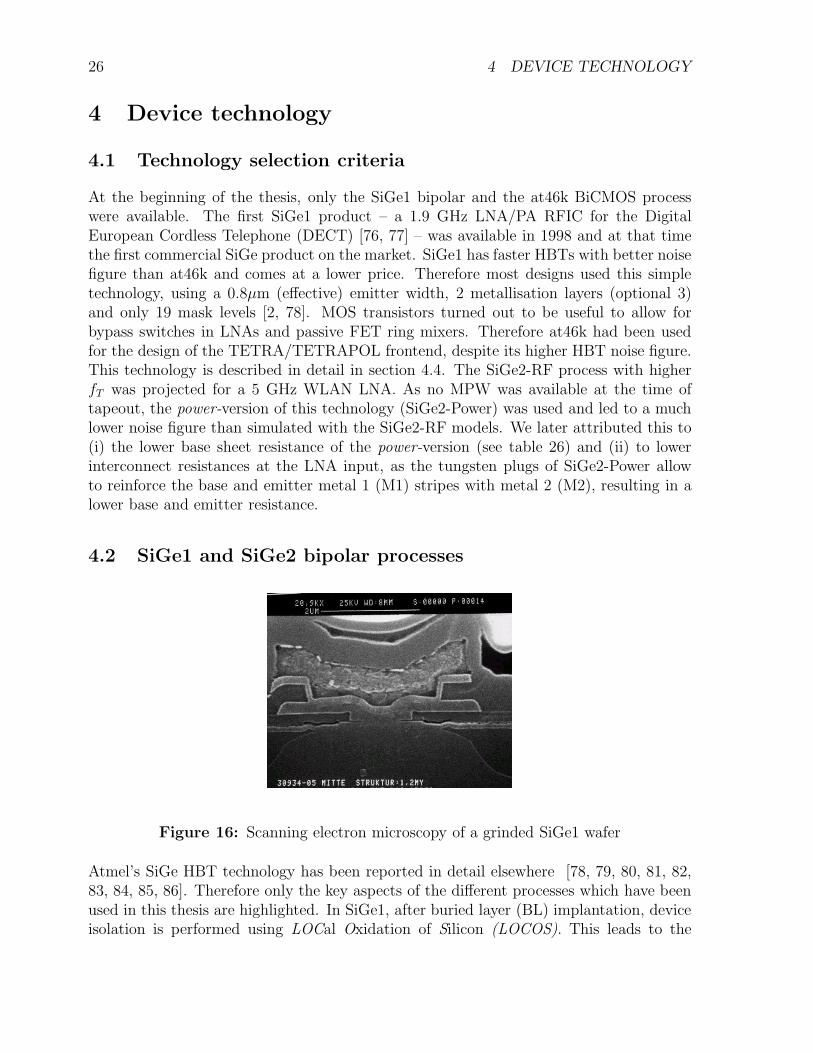
Figure 16: Scanning electron microscopy of a grinded SiGe1 wafer
Atmel’s SiGe HBT technology has been reported in detail elsewhere [78, 79, 80, 81, 82,83, 84, 85, 86]. Therefore only the key aspects of the different processes which have beenused in this thesis are highlighted. In SiGe1, after buried layer (BL) implantation, deviceisolation is performed using LOCal Oxidation of Silicon (LOCOS). This leads to the
4.3 SiGe1 model verification 27
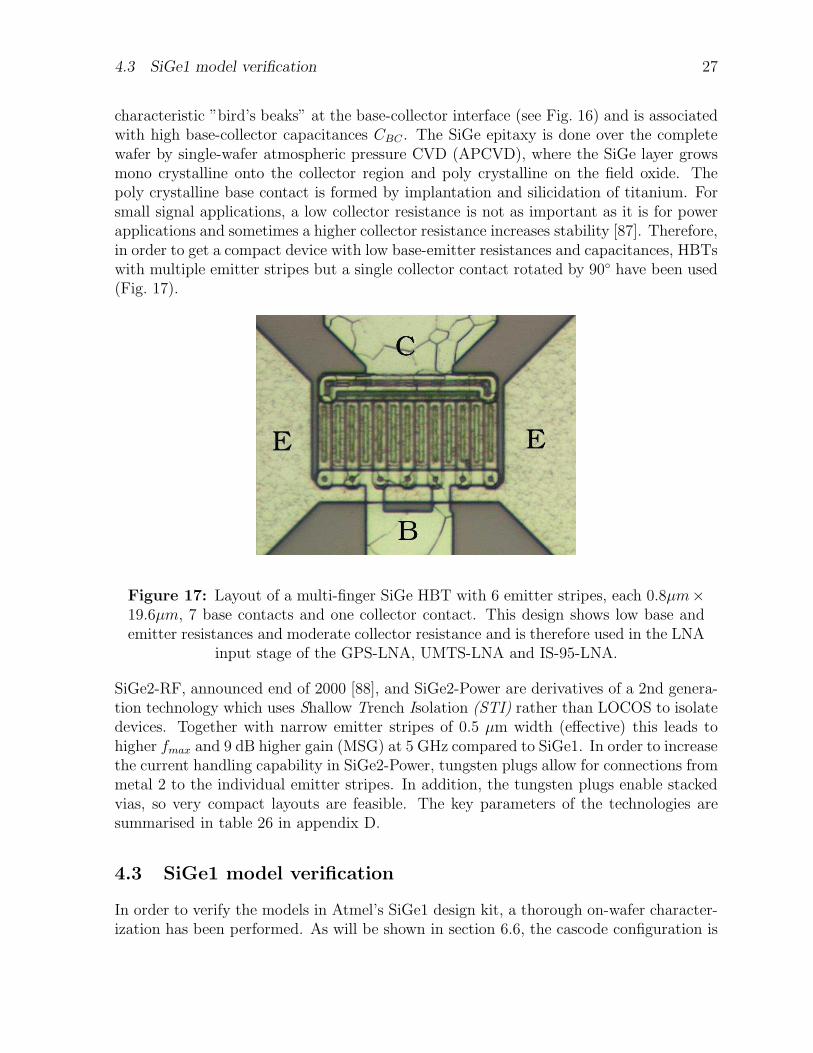
characteristic ”bird’s beaks” at the base-collector interface (see Fig. 16) and is associatedwith high base-collector capacitances CBC . The SiGe epitaxy is done over the completewafer by single-wafer atmospheric pressure CVD (APCVD), where the SiGe layer growsmono crystalline onto the collector region and poly crystalline on the field oxide. Thepoly crystalline base contact is formed by implantation and silicidation of titanium. Forsmall signal applications, a low collector resistance is not as important as it is for powerapplications and sometimes a higher collector resistance increases stability [87]. Therefore,in order to get a compact device with low base-emitter resistances and capacitances, HBTswith multiple emitter stripes but a single collector contact rotated by 90 have been used(Fig. 17).
Figure 17: Layout of a multi-finger SiGe HBT with 6 emitter stripes, each 0.8µm×19.6µm, 7 base contacts and one collector contact. This design shows low base andemitter resistances and moderate collector resistance and is therefore used in the LNA
input stage of the GPS-LNA, UMTS-LNA and IS-95-LNA.
SiGe2-RF, announced end of 2000 [88], and SiGe2-Power are derivatives of a 2nd genera-tion technology which uses Shallow Trench Isolation (STI) rather than LOCOS to isolatedevices. Together with narrow emitter stripes of 0.5 µm width (effective) this leads tohigher fmax and 9 dB higher gain (MSG) at 5 GHz compared to SiGe1. In order to increasethe current handling capability in SiGe2-Power, tungsten plugs allow for connections frommetal 2 to the individual emitter stripes. In addition, the tungsten plugs enable stackedvias, so very compact layouts are feasible. The key parameters of the technologies aresummarised in table 26 in appendix D.
4.3 SiGe1 model verification
In order to verify the models in Atmel’s SiGe1 design kit, a thorough on-wafer character-ization has been performed. As will be shown in section 6.6, the cascode configuration is
28 4 DEVICE TECHNOLOGY
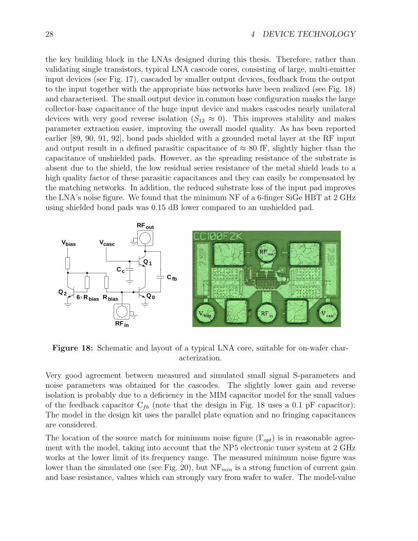
the key building block in the LNAs designed during this thesis. Therefore, rather thanvalidating single transistors, typical LNA cascode cores, consisting of large, multi-emitterinput devices (see Fig. 17), cascaded by smaller output devices, feedback from the outputto the input together with the appropriate bias networks have been realized (see Fig. 18)and characterised. The small output device in common base configuration masks the largecollector-base capacitance of the huge input device and makes cascodes nearly unilateraldevices with very good reverse isolation (S12 ≈ 0). This improves stability and makesparameter extraction easier, improving the overall model quality. As has been reportedearlier [89, 90, 91, 92], bond pads shielded with a grounded metal layer at the RF inputand output result in a defined parasitic capacitance of ≈ 80 fF, slightly higher than thecapacitance of unshielded pads. However, as the spreading resistance of the substrate isabsent due to the shield, the low residual series resistance of the metal shield leads to ahigh quality factor of these parasitic capacitances and they can easily be compensated bythe matching networks. In addition, the reduced substrate loss of the input pad improvesthe LNA’s noise figure. We found that the minimum NF of a 6-finger SiGe HBT at 2 GHzusing shielded bond pads was 0.15 dB lower compared to an unshielded pad.
VcascVbias
outRF
Q0
Q1Cc
RF in
C fb
RbiasQ2
6 RbiasX
Figure 18: Schematic and layout of a typical LNA core, suitable for on-wafer char-acterization.
Very good agreement between measured and simulated small signal S-parameters andnoise parameters was obtained for the cascodes. The slightly lower gain and reverseisolation is probably due to a deficiency in the MIM capacitor model for the small valuesof the feedback capacitor Cfb (note that the design in Fig. 18 uses a 0.1 pF capacitor):The model in the design kit uses the parallel plate equation and no fringing capacitancesare considered.
The location of the source match for minimum noise figure (Γopt) is in reasonable agree-ment with the model, taking into account that the NP5 electronic tuner system at 2 GHzworks at the lower limit of its frequency range. The measured minimum noise figure waslower than the simulated one (see Fig. 20), but NFmin is a strong function of current gainand base resistance, values which can strongly vary from wafer to wafer. The model-value
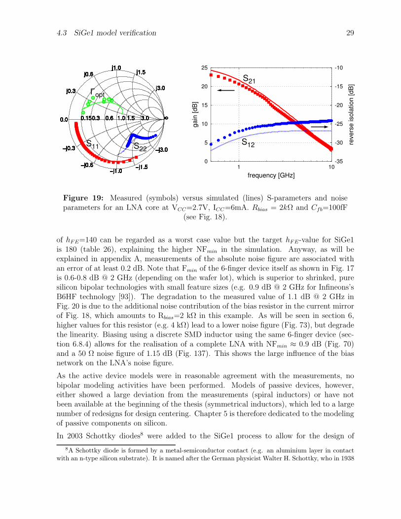
4.3 SiGe1 model verification 29
j0.3
j0.6j1.0
j1.5
j3.0
−j0.3
−j0.6−j1.0
−j1.5
−j3.0
0.150.3 0.6 1.0 1.5 3.00.0 8
j0.3
j0.6j1.0
j1.5
j3.0
−j0.3
−j0.6−j1.0
−j1.5
−j3.0
0.150.3 0.6 1.0 1.5 3.00.0 8
j0.3
j0.6j1.0
j1.5
j3.0
−j0.3
−j0.6−j1.0
−j1.5
−j3.0
0.150.3 0.6 1.0 1.5 3.00.0 8
j0.3
j0.6j1.0
j1.5
j3.0
−j0.3
−j0.6−j1.0
−j1.5
−j3.0
0.150.3 0.6 1.0 1.5 3.00.0 8
j0.3
j0.6j1.0
j1.5
j3.0
−j0.3
−j0.6−j1.0
−j1.5
−j3.0
0.150.3 0.6 1.0 1.5 3.00.0 8
j0.3
j0.6j1.0
j1.5
j3.0
−j0.3
−j0.6−j1.0
−j1.5
−j3.0
0.150.3 0.6 1.0 1.5 3.00.0 8
j0.3
j0.6j1.0
j1.5
j3.0
−j0.3
−j0.6−j1.0
−j1.5
−j3.0
0.150.3 0.6 1.0 1.5 3.00.0 8
j0.3
j0.6j1.0
j1.5
j3.0
−j0.3
−j0.6−j1.0
−j1.5
−j3.0
0.150.3 0.6 1.0 1.5 3.00.0 8
j0.3
j0.6j1.0
j1.5
j3.0
−j0.3
−j0.6−j1.0
−j1.5
−j3.0
0.150.3 0.6 1.0 1.5 3.00.0 8
j0.3
j0.6j1.0
j1.5
j3.0
−j0.3
−j0.6−j1.0
−j1.5
−j3.0
0.150.3 0.6 1.0 1.5 3.00.0 8
j0.3
j0.6j1.0
j1.5
j3.0
−j0.3
−j0.6−j1.0
−j1.5
−j3.0
0.150.3 0.6 1.0 1.5 3.00.0 8
j0.3
j0.6j1.0
j1.5
j3.0
−j0.3
−j0.6−j1.0
−j1.5
−j3.0
0.150.3 0.6 1.0 1.5 3.00.0 8
j0.3
j0.6j1.0
j1.5
j3.0
−j0.3
−j0.6−j1.0
−j1.5
−j3.0
0.150.3 0.6 1.0 1.5 3.00.0 8
j0.3
j0.6j1.0
j1.5
j3.0
−j0.3
−j0.6−j1.0
−j1.5
−j3.0
0.150.3 0.6 1.0 1.5 3.00.0 8
j0.3
j0.6j1.0
j1.5
j3.0
−j0.3
−j0.6−j1.0
−j1.5
−j3.0
0.150.3 0.6 1.0 1.5 3.00.0 8
j0.3
j0.6j1.0
j1.5
j3.0
−j0.3
−j0.6−j1.0
−j1.5
−j3.0
0.150.3 0.6 1.0 1.5 3.00.0 8
j0.3
j0.6j1.0
j1.5
j3.0
−j0.3
−j0.6−j1.0
−j1.5
−j3.0
0.150.3 0.6 1.0 1.5 3.00.0 8
j0.3
j0.6j1.0
j1.5
j3.0
−j0.3
−j0.6−j1.0
−j1.5
−j3.0
0.150.3 0.6 1.0 1.5 3.00.0 8
j0.3
j0.6j1.0
j1.5
j3.0
−j0.3
−j0.6−j1.0
−j1.5
−j3.0
0.150.3 0.6 1.0 1.5 3.00.0 8
S11 S22
Γopt
0
5
10
15
20
25
1 10-35
-30
-25
-20
-15
-10
gain
[dB
]
revers
e isola
tion [dB
]
frequency [GHz]
S21
S12
Figure 19: Measured (symbols) versus simulated (lines) S-parameters and noiseparameters for an LNA core at VCC=2.7V, ICC=6mA. Rbias = 2kΩ and Cfb=100fF
(see Fig. 18).
of hFE=140 can be regarded as a worst case value but the target hFE-value for SiGe1is 180 (table 26), explaining the higher NFmin in the simulation. Anyway, as will beexplained in appendix A, measurements of the absolute noise figure are associated withan error of at least 0.2 dB. Note that Fmin of the 6-finger device itself as shown in Fig. 17is 0.6-0.8 dB @ 2 GHz (depending on the wafer lot), which is superior to shrinked, puresilicon bipolar technologies with small feature sizes (e.g. 0.9 dB @ 2 GHz for Infineons’sB6HF technology [93]). The degradation to the measured value of 1.1 dB @ 2 GHz inFig. 20 is due to the additional noise contribution of the bias resistor in the current mirrorof Fig. 18, which amounts to Rbias=2 kΩ in this example. As will be seen in section 6,higher values for this resistor (e.g. 4 kΩ) lead to a lower noise figure (Fig. 73), but degradethe linearity. Biasing using a discrete SMD inductor using the same 6-finger device (sec-tion 6.8.4) allows for the realisation of a complete LNA with NFmin ≈ 0.9 dB (Fig. 70)and a 50 Ω noise figure of 1.15 dB (Fig. 137). This shows the large influence of the biasnetwork on the LNA’s noise figure.
As the active device models were in reasonable agreement with the measurements, nobipolar modeling activities have been performed. Models of passive devices, however,either showed a large deviation from the measurements (spiral inductors) or have notbeen available at the beginning of the thesis (symmetrical inductors), which led to a largenumber of redesigns for design centering. Chapter 5 is therefore dedicated to the modelingof passive components on silicon.
In 2003 Schottky diodes8 were added to the SiGe1 process to allow for the design of
8A Schottky diode is formed by a metal-semiconductor contact (e.g. an aluminium layer in contactwith an n-type silicon substrate). It is named after the German physicist Walter H. Schottky, who in 1938
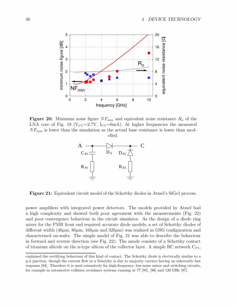
30 4 DEVICE TECHNOLOGY
0
1
2
3
4
5
0 2 4 6 8 100
4
8
12
16
20
min
imum
nois
e fig
ure
[dB
]
equiv
ale
nt nois
e r
esis
tance [
Ω]
frequency [GHz]
NFmin
Rn
Figure 20: Minimum noise figure NFmin and equivalent noise resistance Rn of theLNA core of Fig. 19 (VCC=2.7V, ICC=6mA). At higher frequencies the measuredNFmin is lower than the simulation as the actual base resistance is lower than mod-
elled.
D P2
RP2
D SCP1
RP1
A C
Figure 21: Equivalent circuit model of the Schottky diodes in Atmel’s SiGe1 process.
power amplifiers with integrated power detectors. The models provided by Atmel hada high complexity and showed both poor agreement with the measurements (Fig. 22)and poor convergence behaviour in the circuit simulator. As the design of a diode ringmixer for the PMR front end required accurate diode models, a set of Schottky diodes ofdifferent width (40µm, 80µm, 160µm and 320µm) was realized in GSG configuration andcharacterised on-wafer. The simple model of Fig. 21 was able to describe the behaviourin forward and reverse direction (see Fig. 22): The anode consists of a Schottky contactof titanium silicide on the n-type silicon of the collector layer. A simple RC network CP1,
explained the rectifying behaviour of this kind of contact. The Schottky diode is electrically similar to ap-n junction, though the current flow in a Schottky is due to majority carriers having an inherently fastresponse [94]. Therefore it is used extensively for high-frequency, low-noise mixer and switching circuits,for example in automotive collision avoidance systems running at 77 [95], [96] and 120 GHz [97].
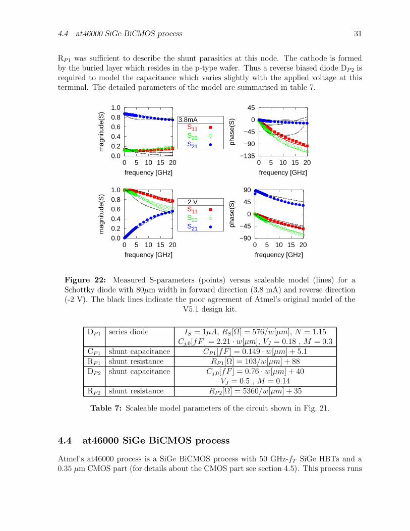
4.4 at46000 SiGe BiCMOS process 31
RP1 was sufficient to describe the shunt parasitics at this node. The cathode is formedby the buried layer which resides in the p-type wafer. Thus a reverse biased diode DP2 isrequired to model the capacitance which varies slightly with the applied voltage at thisterminal. The detailed parameters of the model are summarised in table 7.
0.0
0.2
0.4
0.6
0.8
1.0
0 5 10 15 20
mag
nitu
de(S
)
frequency [GHz]
−2 VS11S22S21
−90
−45
0
45
90
0 5 10 15 20
phas
e(S
)
frequency [GHz]
0.0
0.2
0.4
0.6
0.8
1.0
0 5 10 15 20
mag
nitu
de(S
)
frequency [GHz]
3.8mAS11S22S21
−135
−90
−45
0
45
0 5 10 15 20
phas
e(S
)
frequency [GHz]
Figure 22: Measured S-parameters (points) versus scaleable model (lines) for aSchottky diode with 80µm width in forward direction (3.8 mA) and reverse direction(-2 V). The black lines indicate the poor agreement of Atmel’s original model of the
V5.1 design kit.
DP1 series diode IS = 1µA, RS[Ω] = 576/w[µm], N = 1.15Cj,0[fF ] = 2.21 · w[µm], VJ = 0.18 , M = 0.3
CP1 shunt capacitance CP1[fF ] = 0.149 · w[µm] + 5.1RP1 shunt resistance RP1[Ω] = 103/w[µm] + 88DP2 shunt capacitance Cj,0[fF ] = 0.76 · w[µm] + 40
VJ = 0.5 , M = 0.14RP2 shunt resistance RP2[Ω] = 5360/w[µm] + 35
Table 7: Scaleable model parameters of the circuit shown in Fig. 21.
4.4 at46000 SiGe BiCMOS process
Atmel’s at46000 process is a SiGe BiCMOS process with 50 GHz-fT SiGe HBTs and a0.35 µm CMOS part (for details about the CMOS part see section 4.5). This process runs
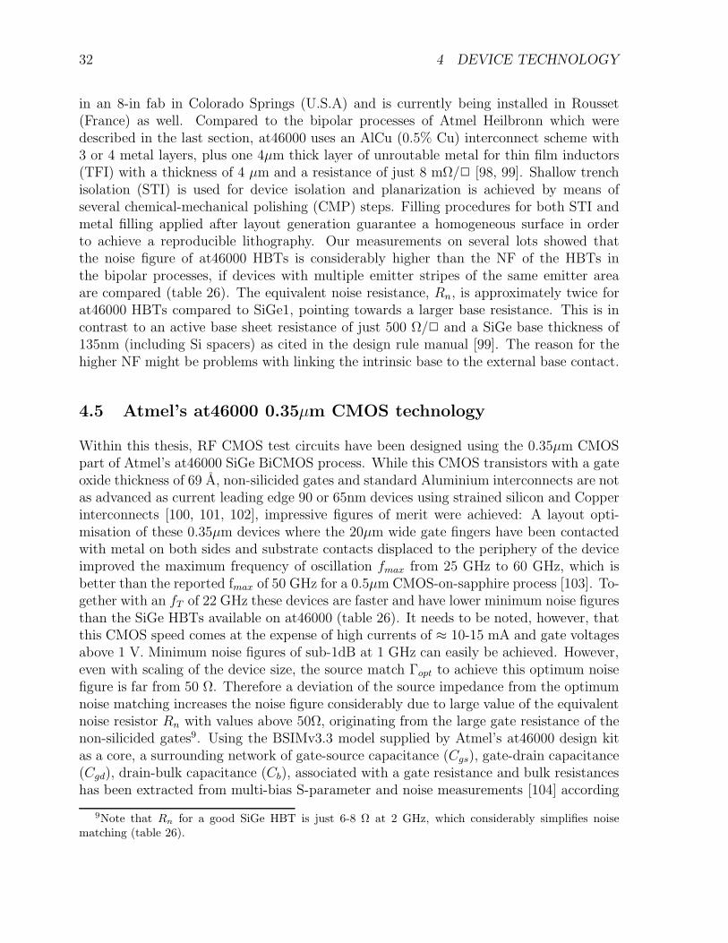
32 4 DEVICE TECHNOLOGY
in an 8-in fab in Colorado Springs (U.S.A) and is currently being installed in Rousset(France) as well. Compared to the bipolar processes of Atmel Heilbronn which weredescribed in the last section, at46000 uses an AlCu (0.5% Cu) interconnect scheme with3 or 4 metal layers, plus one 4µm thick layer of unroutable metal for thin film inductors(TFI) with a thickness of 4 µm and a resistance of just 8 mΩ/2 [98, 99]. Shallow trenchisolation (STI) is used for device isolation and planarization is achieved by means ofseveral chemical-mechanical polishing (CMP) steps. Filling procedures for both STI andmetal filling applied after layout generation guarantee a homogeneous surface in orderto achieve a reproducible lithography. Our measurements on several lots showed thatthe noise figure of at46000 HBTs is considerably higher than the NF of the HBTs inthe bipolar processes, if devices with multiple emitter stripes of the same emitter areaare compared (table 26). The equivalent noise resistance, Rn, is approximately twice forat46000 HBTs compared to SiGe1, pointing towards a larger base resistance. This is incontrast to an active base sheet resistance of just 500 Ω/2 and a SiGe base thickness of135nm (including Si spacers) as cited in the design rule manual [99]. The reason for thehigher NF might be problems with linking the intrinsic base to the external base contact.
4.5 Atmel’s at46000 0.35µm CMOS technology
Within this thesis, RF CMOS test circuits have been designed using the 0.35µm CMOSpart of Atmel’s at46000 SiGe BiCMOS process. While this CMOS transistors with a gateoxide thickness of 69 A, non-silicided gates and standard Aluminium interconnects are notas advanced as current leading edge 90 or 65nm devices using strained silicon and Copperinterconnects [100, 101, 102], impressive figures of merit were achieved: A layout opti-misation of these 0.35µm devices where the 20µm wide gate fingers have been contactedwith metal on both sides and substrate contacts displaced to the periphery of the deviceimproved the maximum frequency of oscillation fmax from 25 GHz to 60 GHz, which isbetter than the reported fmax of 50 GHz for a 0.5µm CMOS-on-sapphire process [103]. To-gether with an fT of 22 GHz these devices are faster and have lower minimum noise figuresthan the SiGe HBTs available on at46000 (table 26). It needs to be noted, however, thatthis CMOS speed comes at the expense of high currents of ≈ 10-15 mA and gate voltagesabove 1 V. Minimum noise figures of sub-1dB at 1 GHz can easily be achieved. However,even with scaling of the device size, the source match Γopt to achieve this optimum noisefigure is far from 50 Ω. Therefore a deviation of the source impedance from the optimumnoise matching increases the noise figure considerably due to large value of the equivalentnoise resistor Rn with values above 50Ω, originating from the large gate resistance of thenon-silicided gates9. Using the BSIMv3.3 model supplied by Atmel’s at46000 design kitas a core, a surrounding network of gate-source capacitance (Cgs), gate-drain capacitance(Cgd), drain-bulk capacitance (Cb), associated with a gate resistance and bulk resistanceshas been extracted from multi-bias S-parameter and noise measurements [104] according
9Note that Rn for a good SiGe HBT is just 6-8 Ω at 2 GHz, which considerably simplifies noisematching (table 26).
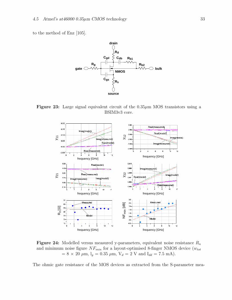
4.5 Atmel’s at46000 0.35µm CMOS technology 33
to the method of Enz [105].
Rg
gdC
Rd
Cdb Rb1
Rb2
sRgsC
drain
NMOSgate bulk
source
Figure 23: Large signal equivalent circuit of the 0.35µm MOS transistors using aBSIM3v3 core.
11y21y
22y12y
min
NF
nR
[Ω]
frequency [GHz]
frequency [GHz]
frequency [GHz]
frequency [GHz]
frequency [GHz]
frequency [GHz]
[dB
]
Figure 24: Modelled versus measured y-parameters, equivalent noise resistance Rn
and minimum noise figure NFmin for a layout-optimised 8-finger NMOS device (wtot
= 8 × 20 µm, lg = 0.35 µm, Vd = 2 V and Idd = 7.5 mA).
The ohmic gate resistance of the MOS devices as extracted from the S-parameter mea-
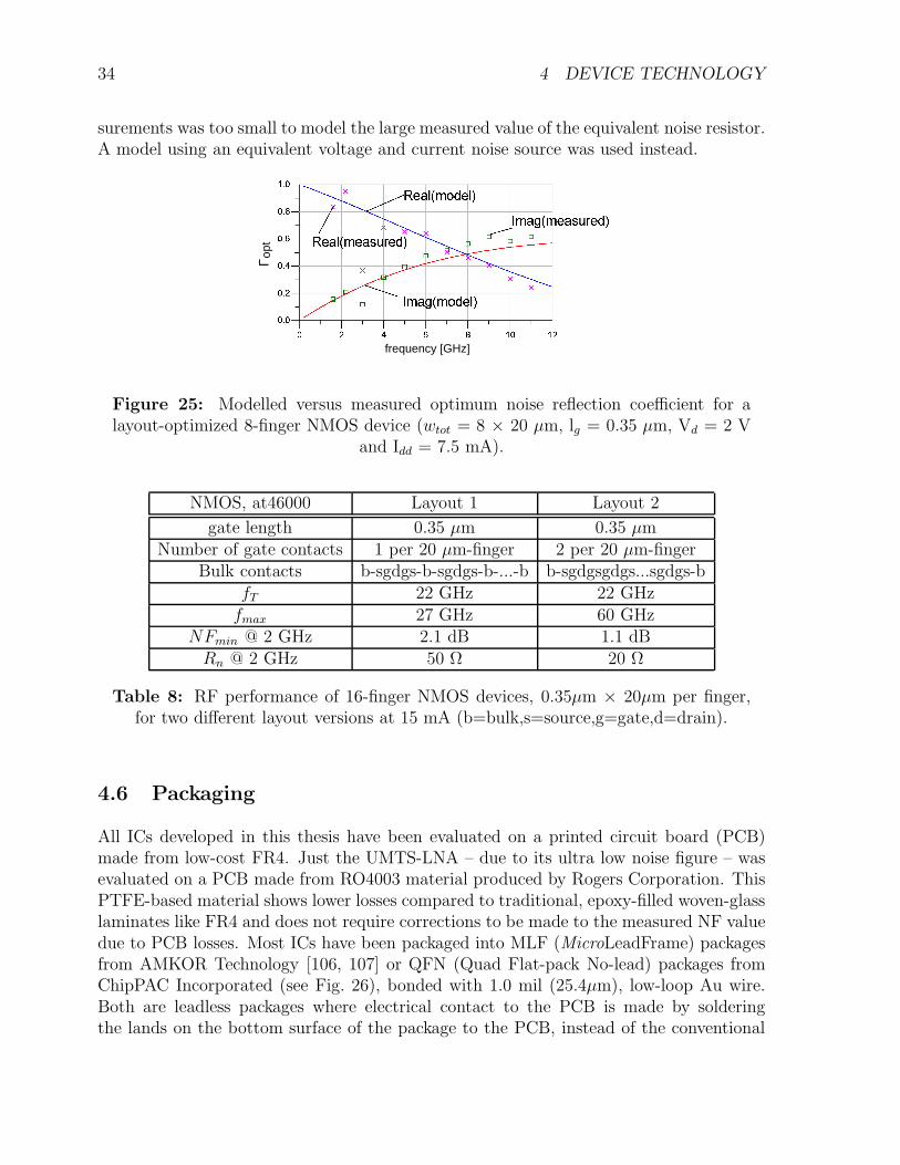
34 4 DEVICE TECHNOLOGY
surements was too small to model the large measured value of the equivalent noise resistor.A model using an equivalent voltage and current noise source was used instead.
frequency [GHz]
opt
Γ
Figure 25: Modelled versus measured optimum noise reflection coefficient for alayout-optimized 8-finger NMOS device (wtot = 8 × 20 µm, lg = 0.35 µm, Vd = 2 V
and Idd = 7.5 mA).
NMOS, at46000 Layout 1 Layout 2
gate length 0.35 µm 0.35 µmNumber of gate contacts 1 per 20 µm-finger 2 per 20 µm-finger
Bulk contacts b-sgdgs-b-sgdgs-b-...-b b-sgdgsgdgs...sgdgs-bfT 22 GHz 22 GHz
fmax 27 GHz 60 GHzNFmin @ 2 GHz 2.1 dB 1.1 dB
Rn @ 2 GHz 50 Ω 20 Ω
Table 8: RF performance of 16-finger NMOS devices, 0.35µm × 20µm per finger,for two different layout versions at 15 mA (b=bulk,s=source,g=gate,d=drain).
4.6 Packaging
All ICs developed in this thesis have been evaluated on a printed circuit board (PCB)made from low-cost FR4. Just the UMTS-LNA – due to its ultra low noise figure – wasevaluated on a PCB made from RO4003 material produced by Rogers Corporation. ThisPTFE-based material shows lower losses compared to traditional, epoxy-filled woven-glasslaminates like FR4 and does not require corrections to be made to the measured NF valuedue to PCB losses. Most ICs have been packaged into MLF (MicroLeadFrame) packagesfrom AMKOR Technology [106, 107] or QFN (Quad Flat-pack No-lead) packages fromChipPAC Incorporated (see Fig. 26), bonded with 1.0 mil (25.4µm), low-loop Au wire.Both are leadless packages where electrical contact to the PCB is made by solderingthe lands on the bottom surface of the package to the PCB, instead of the conventional
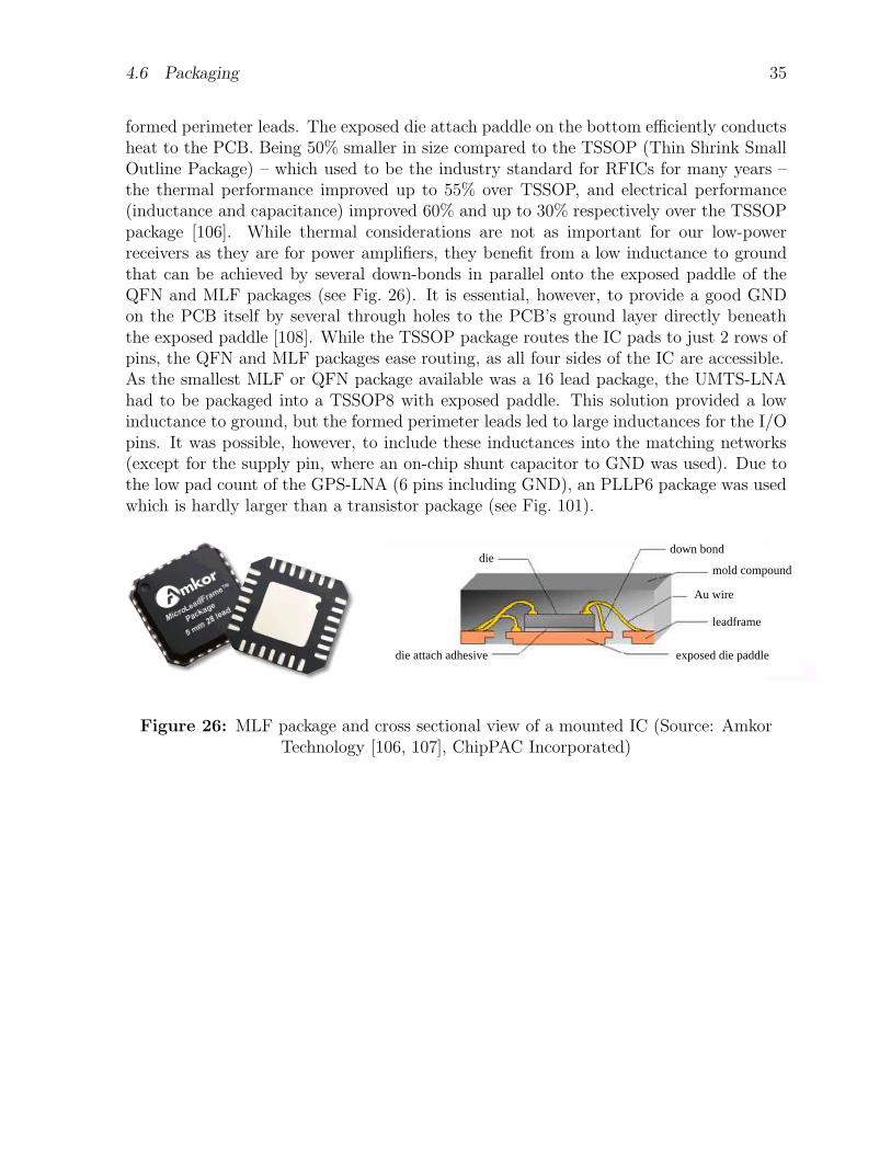
4.6 Packaging 35
formed perimeter leads. The exposed die attach paddle on the bottom efficiently conductsheat to the PCB. Being 50% smaller in size compared to the TSSOP (Thin Shrink SmallOutline Package) – which used to be the industry standard for RFICs for many years –the thermal performance improved up to 55% over TSSOP, and electrical performance(inductance and capacitance) improved 60% and up to 30% respectively over the TSSOPpackage [106]. While thermal considerations are not as important for our low-powerreceivers as they are for power amplifiers, they benefit from a low inductance to groundthat can be achieved by several down-bonds in parallel onto the exposed paddle of theQFN and MLF packages (see Fig. 26). It is essential, however, to provide a good GNDon the PCB itself by several through holes to the PCB’s ground layer directly beneaththe exposed paddle [108]. While the TSSOP package routes the IC pads to just 2 rows ofpins, the QFN and MLF packages ease routing, as all four sides of the IC are accessible.As the smallest MLF or QFN package available was a 16 lead package, the UMTS-LNAhad to be packaged into a TSSOP8 with exposed paddle. This solution provided a lowinductance to ground, but the formed perimeter leads led to large inductances for the I/Opins. It was possible, however, to include these inductances into the matching networks(except for the supply pin, where an on-chip shunt capacitor to GND was used). Due tothe low pad count of the GPS-LNA (6 pins including GND), an PLLP6 package was usedwhich is hardly larger than a transistor package (see Fig. 101).
die attach adhesive
diedown bond
Au wire
leadframe
exposed die paddle
mold compound
Figure 26: MLF package and cross sectional view of a mounted IC (Source: AmkorTechnology [106, 107], ChipPAC Incorporated)
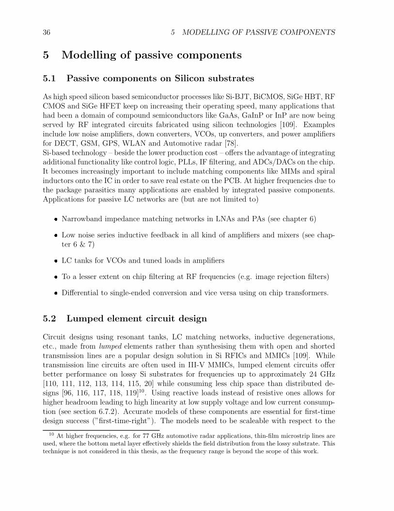
36 5 MODELLING OF PASSIVE COMPONENTS
5 Modelling of passive components
5.1 Passive components on Silicon substrates
As high speed silicon based semiconductor processes like Si-BJT, BiCMOS, SiGe HBT, RFCMOS and SiGe HFET keep on increasing their operating speed, many applications thathad been a domain of compound semiconductors like GaAs, GaInP or InP are now beingserved by RF integrated circuits fabricated using silicon technologies [109]. Examplesinclude low noise amplifiers, down converters, VCOs, up converters, and power amplifiersfor DECT, GSM, GPS, WLAN and Automotive radar [78].Si-based technology – beside the lower production cost – offers the advantage of integratingadditional functionality like control logic, PLLs, IF filtering, and ADCs/DACs on the chip.It becomes increasingly important to include matching components like MIMs and spiralinductors onto the IC in order to save real estate on the PCB. At higher frequencies due tothe package parasitics many applications are enabled by integrated passive components.Applications for passive LC networks are (but are not limited to) Narrowband impedance matching networks in LNAs and PAs (see chapter 6) Low noise series inductive feedback in all kind of amplifiers and mixers (see chap-
ter 6 & 7) LC tanks for VCOs and tuned loads in amplifiers To a lesser extent on chip filtering at RF frequencies (e.g. image rejection filters) Differential to single-ended conversion and vice versa using on chip transformers.
5.2 Lumped element circuit design
Circuit designs using resonant tanks, LC matching networks, inductive degenerations,etc., made from lumped elements rather than synthesising them with open and shortedtransmission lines are a popular design solution in Si RFICs and MMICs [109]. Whiletransmission line circuits are often used in III-V MMICs, lumped element circuits offerbetter performance on lossy Si substrates for frequencies up to approximately 24 GHz[110, 111, 112, 113, 114, 115, 20] while consuming less chip space than distributed de-signs [96, 116, 117, 118, 119]10. Using reactive loads instead of resistive ones allows forhigher headroom leading to high linearity at low supply voltage and low current consump-tion (see section 6.7.2). Accurate models of these components are essential for first-timedesign success (”first-time-right”). The models need to be scaleable with respect to the
10 At higher frequencies, e.g. for 77 GHz automotive radar applications, thin-film microstrip lines areused, where the bottom metal layer effectively shields the field distribution from the lossy substrate. Thistechnique is not considered in this thesis, as the frequency range is beyond the scope of this work.
5.3 Loss mechanisms of passive components on silicon 37
physical geometries in order to allow for fine-tuning of the circuit designs. As popular de-sign environments like Cadence FW2 are based on time-domain-simulators, no frequencydependent elements should be included and the models should be fully SPICE compat-ible. The models for spiral inductors which had been available at the beginning of thethesis in the design kits of Atmel’s SiGe1 and SiGe2 processes lacked accuracy and greatlyoverestimated the quality factor. The quality factor Q is a measure for an inductor’s en-ergy (magnetic energy - electric energy), over the energy dissipated in its metallisationresistance and the conducting substrate (for a detailed definition of Q, see [120] and sec-tion 5.6.). The error in the inductance itself was as large as 30%. This required thatmany circuits, e.g. the LNAs for UMTS and GPS, were realised with several versionson one reticle with slightly different matching networks in order to get one design whichis close to the specification (see chapter 6). For components like symmetrical inductors,no models have been available, leading to time-consuming trial-and-error in the designof the mixers (see chapter 7). The author hopes that this modelling work may lead tobetter agreement between simulated and measured circuit design results, less redesignsand reduced development costs.
5.3 Loss mechanisms of passive components on silicon
It is a common belief that the major challenge of integrating passive components into Si-based processes is the lossy silicon substrate with a specific resistance of ζ = 10−20 Ω ·cmfor bipolar processes and < 5 Ω · cm for CMOS processes: At higher frequencies substratecurrents limit quality factors of integrated inductors due to I2R losses to approximately5-10 [121, 122]. As explained in [123], these currents can be divided into two classes –those conducted through metal-substrate capacitances associated with individual turns ofthe spiral and circulating eddy currents due to magnetic fields within the substrate. Formoderate substrate resistivity (ρ = 10 . . . 30 Ω · cm), eddy currents can be neglected andcurrents conducted through the field oxide into the lossy substrate represent a major lossmechanism [123]. Suspended inductors on a cavity etched underneath through surround-ing via holes have been used in the past to reduce substrate loss and hence increase thequality factor of large-value integrated inductors on a CMOS substrate [91, 124, 125, 109],but this technique did not become a mainstream process due to concerns about the sta-bility of the membrane11. In section 5.11 we examined suspended inductors realised bybackside etching on SiGe2-Power and SiGe2-RF processes and came to the conclusionthat etched cavities make sense for large inductors only (2πf · L > 50 Ω, where f isthe operating frequency). To reduce inter stage matching losses of power amplifiers andbipolar LNAs and mixers, however, small inductors (2πf ·L < 50 Ω) are required, due to
11 Recently, techniques have been presented that transfer a fully processed silicon wafer onto a low-lossglass substrate or even a flex foil by using a substrate transfer process with removal of the lossy siliconsubstrate at a delamination layer like the buried oxide of a SIMOX wafer [126, 127], resulting in valuesfor the quality factor of up to 40. Proton implantation selectively below passive structures – a methodoriginally used for GaAs HBT isolation – can create semi-insulating (≈ 106Ω · cm) Si layers and increasesthe Q factor for 5-15 nH inductors by 30-60% [128].
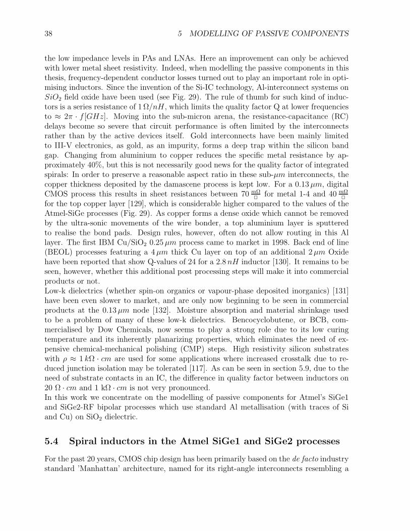
38 5 MODELLING OF PASSIVE COMPONENTS
the low impedance levels in PAs and LNAs. Here an improvement can only be achievedwith lower metal sheet resistivity. Indeed, when modelling the passive components in thisthesis, frequency-dependent conductor losses turned out to play an important role in opti-mising inductors. Since the invention of the Si-IC technology, Al-interconnect systems onSiO2 field oxide have been used (see Fig. 29). The rule of thumb for such kind of induc-tors is a series resistance of 1 Ω/nH , which limits the quality factor Q at lower frequenciesto ≈ 2π · f [GHz]. Moving into the sub-micron arena, the resistance-capacitance (RC)delays become so severe that circuit performance is often limited by the interconnectsrather than by the active devices itself. Gold interconnects have been mainly limitedto III-V electronics, as gold, as an impurity, forms a deep trap within the silicon bandgap. Changing from aluminium to copper reduces the specific metal resistance by ap-proximately 40%, but this is not necessarily good news for the quality factor of integratedspirals: In order to preserve a reasonable aspect ratio in these sub-µm interconnects, thecopper thickness deposited by the damascene process is kept low. For a 0.13 µm, digitalCMOS process this results in sheet resistances between 70 mΩ
2for metal 1-4 and 40 mΩ
2
for the top copper layer [129], which is considerable higher compared to the values of theAtmel-SiGe processes (Fig. 29). As copper forms a dense oxide which cannot be removedby the ultra-sonic movements of the wire bonder, a top aluminium layer is sputteredto realise the bond pads. Design rules, however, often do not allow routing in this Allayer. The first IBM Cu/SiO2 0.25 µm process came to market in 1998. Back end of line(BEOL) processes featuring a 4 µm thick Cu layer on top of an additional 2 µm Oxidehave been reported that show Q-values of 24 for a 2.8 nH inductor [130]. It remains to beseen, however, whether this additional post processing steps will make it into commercialproducts or not.Low-k dielectrics (whether spin-on organics or vapour-phase deposited inorganics) [131]have been even slower to market, and are only now beginning to be seen in commercialproducts at the 0.13 µm node [132]. Moisture absorption and material shrinkage usedto be a problem of many of these low-k dielectrics. Bencocyclobutene, or BCB, com-mercialised by Dow Chemicals, now seems to play a strong role due to its low curingtemperature and its inherently planarizing properties, which eliminates the need of ex-pensive chemical-mechanical polishing (CMP) steps. High resistivity silicon substrateswith ρ ≈ 1 kΩ · cm are used for some applications where increased crosstalk due to re-duced junction isolation may be tolerated [117]. As can be seen in section 5.9, due to theneed of substrate contacts in an IC, the difference in quality factor between inductors on20 Ω · cm and 1 kΩ · cm is not very pronounced.In this work we concentrate on the modelling of passive components for Atmel’s SiGe1and SiGe2-RF bipolar processes which use standard Al metallisation (with traces of Siand Cu) on SiO2 dielectric.
5.4 Spiral inductors in the Atmel SiGe1 and SiGe2 processes
For the past 20 years, CMOS chip design has been primarily based on the de facto industrystandard ’Manhattan’ architecture, named for its right-angle interconnects resembling a
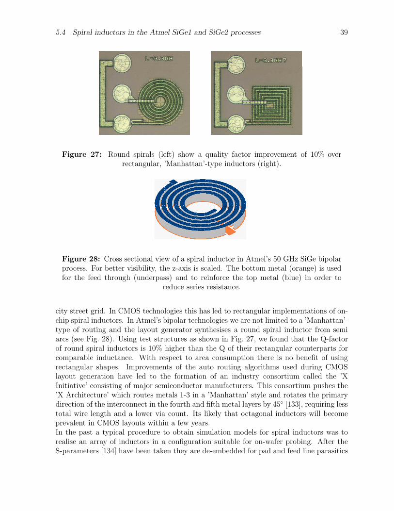
5.4 Spiral inductors in the Atmel SiGe1 and SiGe2 processes 39
Figure 27: Round spirals (left) show a quality factor improvement of 10% overrectangular, ’Manhattan’-type inductors (right).
Figure 28: Cross sectional view of a spiral inductor in Atmel’s 50 GHz SiGe bipolarprocess. For better visibility, the z-axis is scaled. The bottom metal (orange) is usedfor the feed through (underpass) and to reinforce the top metal (blue) in order to
reduce series resistance.
city street grid. In CMOS technologies this has led to rectangular implementations of on-chip spiral inductors. In Atmel’s bipolar technologies we are not limited to a ’Manhattan’-type of routing and the layout generator synthesises a round spiral inductor from semiarcs (see Fig. 28). Using test structures as shown in Fig. 27, we found that the Q-factorof round spiral inductors is 10% higher than the Q of their rectangular counterparts forcomparable inductance. With respect to area consumption there is no benefit of usingrectangular shapes. Improvements of the auto routing algorithms used during CMOSlayout generation have led to the formation of an industry consortium called the ’XInitiative’ consisting of major semiconductor manufacturers. This consortium pushes the’X Architecture’ which routes metals 1-3 in a ’Manhattan’ style and rotates the primarydirection of the interconnect in the fourth and fifth metal layers by 45 [133], requiring lesstotal wire length and a lower via count. Its likely that octagonal inductors will becomeprevalent in CMOS layouts within a few years.In the past a typical procedure to obtain simulation models for spiral inductors was torealise an array of inductors in a configuration suitable for on-wafer probing. After theS-parameters [134] have been taken they are de-embedded for pad and feed line parasitics
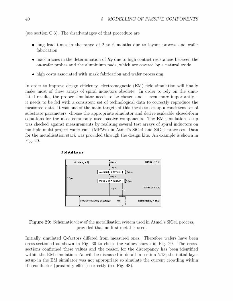
40 5 MODELLING OF PASSIVE COMPONENTS
(see section C.3). The disadvantages of that procedure are long lead times in the range of 2 to 6 months due to layout process and waferfabrication inaccuracies in the determination of RS due to high contact resistances between theon-wafer probes and the aluminium pads, which are covered by a natural oxide high costs associated with mask fabrication and wafer processing.
In order to improve design efficiency, electromagnetic (EM) field simulation will finallymake most of these arrays of spiral inductors obsolete. In order to rely on the simu-lated results, the proper simulator needs to be chosen and – even more importantly –it needs to be fed with a consistent set of technological data to correctly reproduce themeasured data. It was one of the main targets of this thesis to set-up a consistent set ofsubstrate parameters, choose the appropriate simulator and derive scaleable closed-formequations for the most commonly used passive components. The EM simulation setupwas checked against measurements by realising several test arrays of spiral inductors onmultiple multi-project wafer runs (MPWs) in Atmel’s SiGe1 and SiGe2 processes. Datafor the metallisation stack was provided through the design kits. An example is shown inFig. 29.
Figure 29: Schematic view of the metallisation system used in Atmel’s SiGe1 process,provided that no first metal is used.
Initially simulated Q-factors differed from measured ones. Therefore wafers have beencross-sectioned as shown in Fig. 30 to check the values shown in Fig. 29. The cross-sections confirmed these values and the reason for the discrepancy has been identifiedwithin the EM simulation: As will be discussed in detail in section 5.13, the initial layersetup in the EM simulator was not appropriate so simulate the current crowding withinthe conductor (proximity effect) correctly (see Fig. 48).
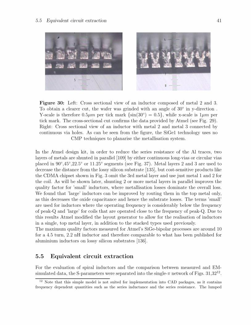
5.5 Equivalent circuit extraction 41
Figure 30: Left: Cross sectional view of an inductor composed of metal 2 and 3.To obtain a clearer cut, the wafer was grinded with an angle of 30 in y-direction .Y-scale is therefore 0.5µm per tick mark sin(30) = 0.5, while x-scale is 1µm pertick mark. The cross-sectional cut confirms the data provided by Atmel (see Fig. 29).Right: Cross sectional view of an inductor with metal 2 and metal 3 connected bycontinuous via holes. As can be seen from the figure, the SiGe1 technology uses no
CMP techniques to planarise the metallisation system.
In the Atmel design kit, in order to reduce the series resistance of the Al traces, twolayers of metals are shunted in parallel [109] by either continuous long-vias or circular viasplaced in 90,45,22.5 or 11.25 segments (see Fig. 37). Metal layers 2 and 3 are used todecrease the distance from the lossy silicon substrate [135], but cost-sensitive products likethe CDMA chipset shown in Fig. 3 omit the 3rd metal layer and use just metal 1 and 2 forthe coil. As will be shown later, shunting 2 or more metal layers in parallel improves thequality factor for ’small’ inductors, where metallisation losses dominate the overall loss.We found that ’large’ inductors can be improved by routing them in the top metal only,as this decreases the oxide capacitance and hence the substrate losses. The terms ’small’are used for inductors where the operating frequency is considerably below the frequencyof peak-Q and ’large’ for coils that are operated close to the frequency of peak-Q. Due tothis results Atmel modified the layout generator to allow for the realisation of inductorsin a single, top metal layer, in addition to the stacked types used previously.The maximum quality factors measured for Atmel’s SiGe-bipolar processes are around 10for a 4.5 turn, 2.2 nH inductor and therefore comparable to what has been published foraluminium inductors on lossy silicon substrates [136].
5.5 Equivalent circuit extraction
For the evaluation of spiral inductors and the comparison between measured and EM-simulated data, the S-parameters were separated into the single-π network of Figs. 31,3212.
12 Note that this simple model is not suited for implementation into CAD packages, as it containsfrequency dependent quantities such as the series inductance and the series resistance. The lumped
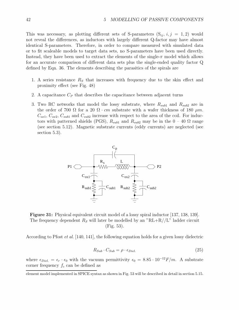
42 5 MODELLING OF PASSIVE COMPONENTS
This was necessary, as plotting different sets of S-parameters (Sij , i, j = 1, 2) wouldnot reveal the differences, as inductors with largely different Q-factor may have almostidentical S-parameters. Therefore, in order to compare measured with simulated dataor to fit scaleable models to target data sets, no S-parameters have been used directly.Instead, they have been used to extract the elements of the single-π model which allowsfor an accurate comparison of different data sets plus the single-ended quality factor Qdefined by Eqn. 36. The elements describing the parasitics of the spirals are
1. A series resistance RS that increases with frequency due to the skin effect andproximity effect (see Fig. 48)
2. A capacitance CP that describes the capacitance between adjacent turns
3. Two RC networks that model the lossy substrate, where Rsub1 and Rsub2 are inthe order of 700 Ω for a 20 Ω · cm substrate with a wafer thickness of 180 µm.Cox1, Cox2, Csub1 and Csub2 increase with respect to the area of the coil. For induc-tors with patterned shields (PGS), Rsub1 and Rsub2 may be in the 0 – 40 Ω range(see section 5.12). Magnetic substrate currents (eddy currents) are neglected (seesection 5.3).
ox1C ox2C
sub1R sub2Rsub1C sub2C
pC
sR LP2P1
Figure 31: Physical equivalent circuit model of a lossy spiral inductor [137, 138, 139].The frequency dependent RS will later be modelled by an ”RL+R//L” ladder circuit
(Fig. 53).
According to Pfost et al. [140, 141], the following equation holds for a given lossy dielectric
RSub · CSub = ρ · εDiel. (25)
where εDiel. = εr · ε0 with the vacuum permittivity ε0 = 8.85 · 10−12F/m. A substratecorner frequency fc can be defined as
element model implemented in SPICE syntax as shown in Fig. 53 will be described in detail in section 5.15.
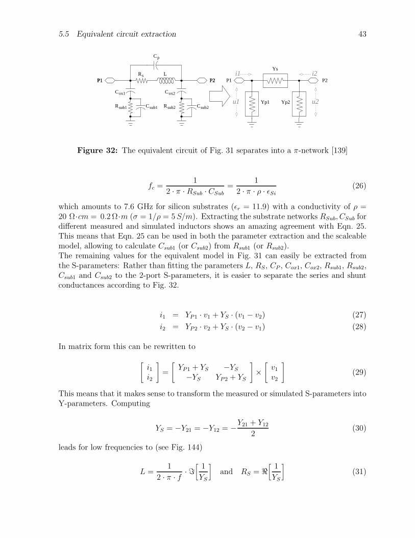
5.5 Equivalent circuit extraction 43
ox1C ox2C
sub1R sub2Rsub1C sub2C
pC
sR LP2P1 P2P1 P2P1
Ys
Yp1u1
i1
u2Yp2
i2
Figure 32: The equivalent circuit of Fig. 31 separates into a π-network [139]
fc =1
2 · π · RSub · CSub=
1
2 · π · ρ · εSi(26)
which amounts to 7.6 GHz for silicon substrates (εr = 11.9) with a conductivity of ρ =20 Ω·cm = 0.2 Ω·m (σ = 1/ρ = 5 S/m). Extracting the substrate networks RSub, CSub fordifferent measured and simulated inductors shows an amazing agreement with Eqn. 25.This means that Eqn. 25 can be used in both the parameter extraction and the scaleablemodel, allowing to calculate Csub1 (or Csub2) from Rsub1 (or Rsub2).The remaining values for the equivalent model in Fig. 31 can easily be extracted fromthe S-parameters: Rather than fitting the parameters L, RS, CP , Cox1, Cox2, Rsub1, Rsub2,Csub1 and Csub2 to the 2-port S-parameters, it is easier to separate the series and shuntconductances according to Fig. 32.
i1 = YP1 · v1 + YS · (v1 − v2) (27)
i2 = YP2 · v2 + YS · (v2 − v1) (28)
In matrix form this can be rewritten to
[
i1i2
]
=
[
YP1 + YS −YS
−YS YP2 + YS
]
×[
v1
v2
]
(29)
This means that it makes sense to transform the measured or simulated S-parameters intoY-parameters. Computing
YS = −Y21 = −Y12 = −Y21 + Y12
2(30)
leads for low frequencies to (see Fig. 144)
L =1
2 · π · f · =[
1
YS
]
and RS = <[
1
YS
]
(31)
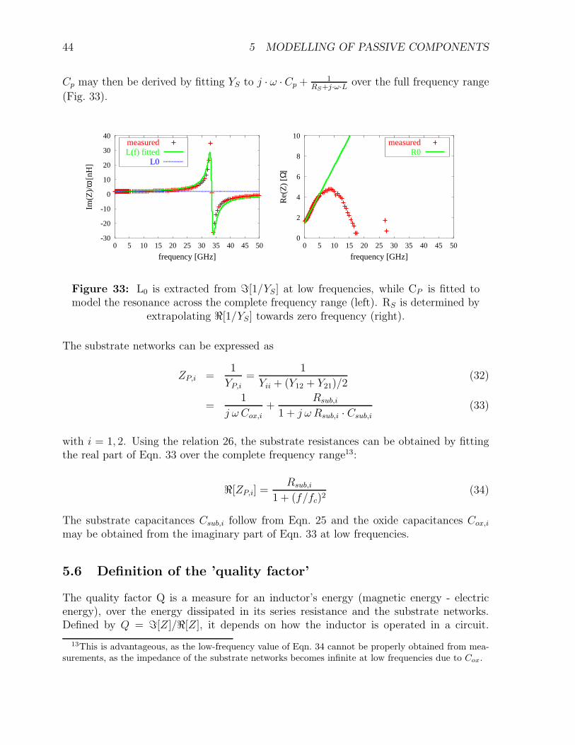
44 5 MODELLING OF PASSIVE COMPONENTS
Cp may then be derived by fitting YS to j · ω ·Cp + 1RS+j·ω·L
over the full frequency range
(Fig. 33).
-30
-20
-10
0
10
20
30
40
0 5 10 15 20 25 30 35 40 45 50
Im(Z
)/ω
[nH
]
frequency [GHz]
measuredL(f) fitted
L0
0
2
4
6
8
10
0 5 10 15 20 25 30 35 40 45 50
Re(
Z)
[Ω]
frequency [GHz]
measuredR0
Figure 33: L0 is extracted from =[1/YS] at low frequencies, while CP is fitted tomodel the resonance across the complete frequency range (left). RS is determined by
extrapolating <[1/YS] towards zero frequency (right).
The substrate networks can be expressed as
ZP,i =1
YP,i=
1
Yii + (Y12 + Y21)/2(32)
=1
j ω Cox,i+
Rsub,i
1 + j ω Rsub,i · Csub,i(33)
with i = 1, 2. Using the relation 26, the substrate resistances can be obtained by fittingthe real part of Eqn. 33 over the complete frequency range13:
<[ZP,i] =Rsub,i
1 + (f/fc)2(34)
The substrate capacitances Csub,i follow from Eqn. 25 and the oxide capacitances Cox,i
may be obtained from the imaginary part of Eqn. 33 at low frequencies.
5.6 Definition of the ’quality factor’
The quality factor Q is a measure for an inductor’s energy (magnetic energy - electricenergy), over the energy dissipated in its series resistance and the substrate networks.Defined by Q = =[Z]/<[Z], it depends on how the inductor is operated in a circuit.
13This is advantageous, as the low-frequency value of Eqn. 34 cannot be properly obtained from mea-surements, as the impedance of the substrate networks becomes infinite at low frequencies due to Cox.
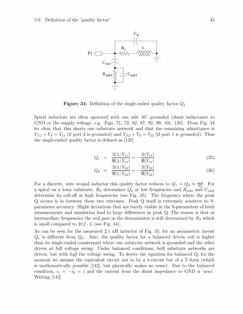
5.6 Definition of the ’quality factor’ 45
ox1C
sub1R sub1C
pC
sR LP1
Figure 34: Definition of the single-ended quality factor Q1
Spiral inductors are often operated with one side AC grounded (shunt inductance toGND or the supply voltage, e.g. Figs. 71, 72, 82, 87, 92, 99, 101, 120). From Fig. 34its clear that this shorts one substrate network and that the remaining admittance isYP,1 + YS = Y11 (if port 2 is grounded) and YP,2 + YS = Y22 (if port 1 is grounded). Thusthe single-ended quality factor is defined as [120]
Q1 ==(1/Y11)
<(1/Y11)= −=(Y11)
<(Y11)(35)
Q2 ==(1/Y22)
<(1/Y22)= −=(Y22)
<(Y22)(36)
For a discrete, wire wound inductor this quality factor reduces to Q1 = Q2 ≈ ω·LRS
. Fora spiral on a lossy substrate, RS determines Q1 at low frequencies and Rsub1 and Csub1
determine its roll-off at high frequencies (see Fig. 35). The frequency where the peakQ occurs is in between these two extremes. Peak Q itself is extremely sensitive to S-parameter accuracy: Slight deviations that are barely visible in the S-parameters of bothmeasurements and simulation lead to large differences in peak Q. The reason is that atintermediate frequencies the real part in the denominator is still determined by RS whichis small compared to 2πf · L (see Fig. 34).
As can be seen for the measured 2.1 nH inductor of Fig. 35, for an asymmetric layoutQ1 is different from Q2. Also, the quality factor for a balanced driven coil is higherthan its single-ended counterpart where one substrate network is grounded and the otherdriven at full voltage swing: Under balanced conditions, both substrate networks aredriven, but with half the voltage swing. To derive the equation for balanced Q, for themoment we assume the equivalent circuit not to be a π-circuit but of a T -form (whichis mathematically possible [142], but physically makes no sense). Due to the balancedcondition, i1 = −i2 = i and the current from the shunt impedance to GND is ’zero’.Writing [142]
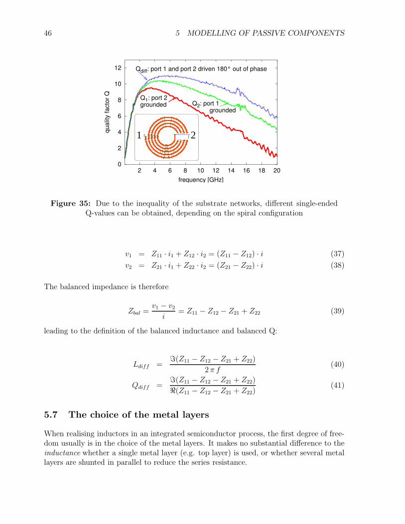
46 5 MODELLING OF PASSIVE COMPONENTS
0
2
4
6
8
10
12
2 4 6 8 10 12 14 16 18 20
qu
alit
y f
acto
r Q
frequency [GHz]
Q1: port 2grounded Q2: port 1
grounded
Qdiff: port 1 and port 2 driven 180° out of phase
21
Figure 35: Due to the inequality of the substrate networks, different single-endedQ-values can be obtained, depending on the spiral configuration
v1 = Z11 · i1 + Z12 · i2 = (Z11 − Z12) · i (37)
v2 = Z21 · i1 + Z22 · i2 = (Z21 − Z22) · i (38)
The balanced impedance is therefore
Zbal =v1 − v2
i= Z11 − Z12 − Z21 + Z22 (39)
leading to the definition of the balanced inductance and balanced Q:
Ldiff ==(Z11 − Z12 − Z21 + Z22)
2 π f(40)
Qdiff ==(Z11 − Z12 − Z21 + Z22)
<(Z11 − Z12 − Z21 + Z22)(41)
5.7 The choice of the metal layers
When realising inductors in an integrated semiconductor process, the first degree of free-dom usually is in the choice of the metal layers. It makes no substantial difference to theinductance whether a single metal layer (e.g. top layer) is used, or whether several metallayers are shunted in parallel to reduce the series resistance.
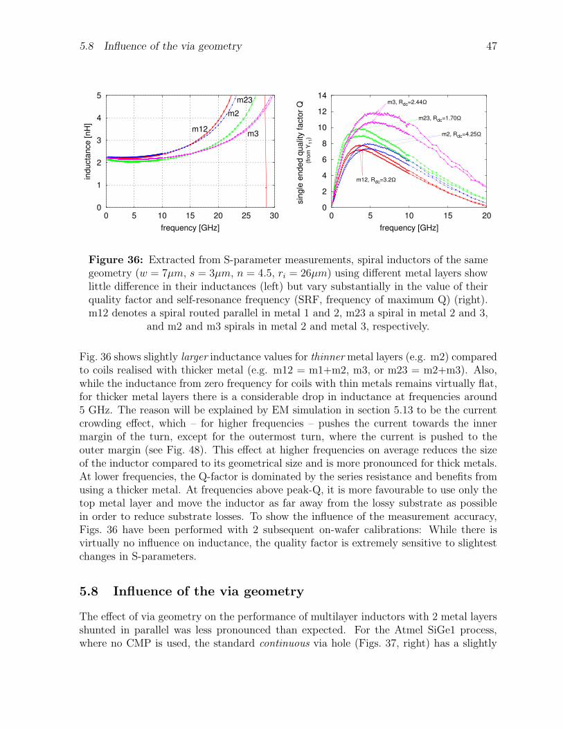
5.8 Influence of the via geometry 47
0
1
2
3
4
5
0 5 10 15 20 25 30
inducta
nce [nH
]
frequency [GHz]
m23
m3
m2
m12
0
2
4
6
8
10
12
14
0 5 10 15 20
sin
gle
ended q
ualit
y facto
r Q
(
fro
m Y
11)
frequency [GHz]
m3, Rdc=2.44Ω
m23, Rdc=1.70Ω
m2, Rdc=4.25Ω
m12, Rdc=3.2Ω
Figure 36: Extracted from S-parameter measurements, spiral inductors of the samegeometry (w = 7µm, s = 3µm, n = 4.5, ri = 26µm) using different metal layers showlittle difference in their inductances (left) but vary substantially in the value of theirquality factor and self-resonance frequency (SRF, frequency of maximum Q) (right).m12 denotes a spiral routed parallel in metal 1 and 2, m23 a spiral in metal 2 and 3,
and m2 and m3 spirals in metal 2 and metal 3, respectively.
Fig. 36 shows slightly larger inductance values for thinner metal layers (e.g. m2) comparedto coils realised with thicker metal (e.g. m12 = m1+m2, m3, or m23 = m2+m3). Also,while the inductance from zero frequency for coils with thin metals remains virtually flat,for thicker metal layers there is a considerable drop in inductance at frequencies around5 GHz. The reason will be explained by EM simulation in section 5.13 to be the currentcrowding effect, which – for higher frequencies – pushes the current towards the innermargin of the turn, except for the outermost turn, where the current is pushed to theouter margin (see Fig. 48). This effect at higher frequencies on average reduces the sizeof the inductor compared to its geometrical size and is more pronounced for thick metals.At lower frequencies, the Q-factor is dominated by the series resistance and benefits fromusing a thicker metal. At frequencies above peak-Q, it is more favourable to use only thetop metal layer and move the inductor as far away from the lossy substrate as possiblein order to reduce substrate losses. To show the influence of the measurement accuracy,Figs. 36 have been performed with 2 subsequent on-wafer calibrations: While there isvirtually no influence on inductance, the quality factor is extremely sensitive to slightestchanges in S-parameters.
5.8 Influence of the via geometry
The effect of via geometry on the performance of multilayer inductors with 2 metal layersshunted in parallel was less pronounced than expected. For the Atmel SiGe1 process,where no CMP is used, the standard continuous via hole (Figs. 37, right) has a slightly
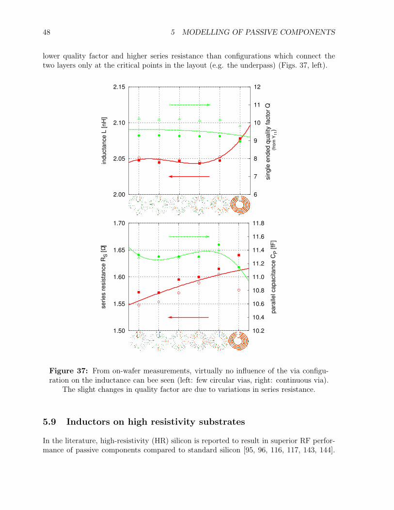
48 5 MODELLING OF PASSIVE COMPONENTS
lower quality factor and higher series resistance than configurations which connect thetwo layers only at the critical points in the layout (e.g. the underpass) (Figs. 37, left).
2.00
2.05
2.10
2.15
1 2 3 4 5 66
7
8
9
10
11
12
inducta
nce L
[nH
]
sin
gle
ended q
ualit
y facto
r Q
(
fro
m Y
11)
1.50
1.55
1.60
1.65
1.70
1 2 3 4 5 610.2
10.4
10.6
10.8
11.0
11.2
11.4
11.6
11.8
series r
esis
tance R
S [
Ω]
para
llel capacitance C
P [fF
]
Figure 37: From on-wafer measurements, virtually no influence of the via configu-ration on the inductance can bee seen (left: few circular vias, right: continuous via).
The slight changes in quality factor are due to variations in series resistance.
5.9 Inductors on high resistivity substrates
In the literature, high-resistivity (HR) silicon is reported to result in superior RF perfor-mance of passive components compared to standard silicon [95, 96, 116, 117, 143, 144].
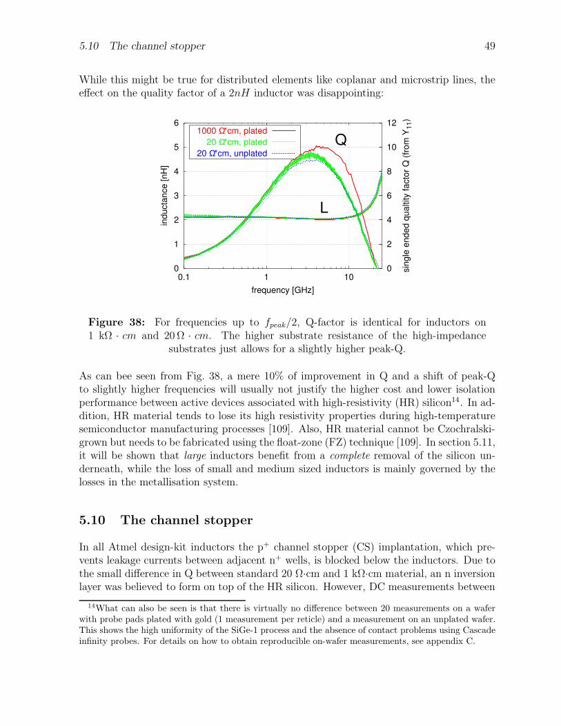
5.10 The channel stopper 49
While this might be true for distributed elements like coplanar and microstrip lines, theeffect on the quality factor of a 2nH inductor was disappointing:
0
1
2
3
4
5
6
0.1 1 100
2
4
6
8
10
12
ind
ucta
nce
[n
H]
sin
gle
en
de
d q
ua
ltity f
acto
r Q
(fr
om
Y11)
frequency [GHz]
L
Q1000 Ω*cm, plated
20 Ω*cm, plated
20 Ω*cm, unplated
Figure 38: For frequencies up to fpeak/2, Q-factor is identical for inductors on1 kΩ · cm and 20 Ω · cm. The higher substrate resistance of the high-impedance
substrates just allows for a slightly higher peak-Q.
As can bee seen from Fig. 38, a mere 10% of improvement in Q and a shift of peak-Qto slightly higher frequencies will usually not justify the higher cost and lower isolationperformance between active devices associated with high-resistivity (HR) silicon14. In ad-dition, HR material tends to lose its high resistivity properties during high-temperaturesemiconductor manufacturing processes [109]. Also, HR material cannot be Czochralski-grown but needs to be fabricated using the float-zone (FZ) technique [109]. In section 5.11,it will be shown that large inductors benefit from a complete removal of the silicon un-derneath, while the loss of small and medium sized inductors is mainly governed by thelosses in the metallisation system.
5.10 The channel stopper
In all Atmel design-kit inductors the p+ channel stopper (CS) implantation, which pre-vents leakage currents between adjacent n+ wells, is blocked below the inductors. Due tothe small difference in Q between standard 20 Ω·cm and 1 kΩ·cm material, an n inversionlayer was believed to form on top of the HR silicon. However, DC measurements between
14What can also be seen is that there is virtually no difference between 20 measurements on a waferwith probe pads plated with gold (1 measurement per reticle) and a measurement on an unplated wafer.This shows the high uniformity of the SiGe-1 process and the absence of contact problems using Cascadeinfinity probes. For details on how to obtain reproducible on-wafer measurements, see appendix C.
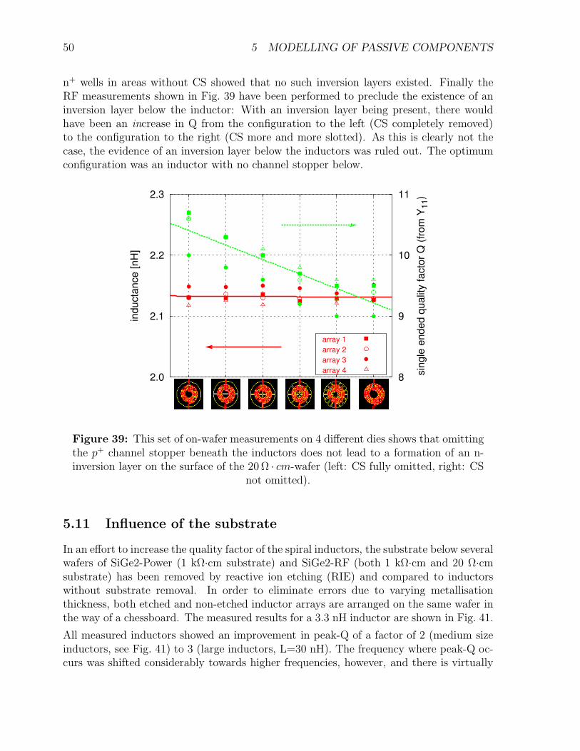
50 5 MODELLING OF PASSIVE COMPONENTS
n+ wells in areas without CS showed that no such inversion layers existed. Finally theRF measurements shown in Fig. 39 have been performed to preclude the existence of aninversion layer below the inductor: With an inversion layer being present, there wouldhave been an increase in Q from the configuration to the left (CS completely removed)to the configuration to the right (CS more and more slotted). As this is clearly not thecase, the evidence of an inversion layer below the inductors was ruled out. The optimumconfiguration was an inductor with no channel stopper below.
2.0
2.1
2.2
2.3
1 2 3 4 5 68
9
10
11
ind
ucta
nce
[n
H]
sin
gle
en
de
d q
ua
lity f
acto
r Q
(fr
om
Y1
1)
array 1
array 2
array 3
array 4
Figure 39: This set of on-wafer measurements on 4 different dies shows that omittingthe p+ channel stopper beneath the inductors does not lead to a formation of an n-inversion layer on the surface of the 20 Ω · cm-wafer (left: CS fully omitted, right: CS
not omitted).
5.11 Influence of the substrate
In an effort to increase the quality factor of the spiral inductors, the substrate below severalwafers of SiGe2-Power (1 kΩ·cm substrate) and SiGe2-RF (both 1 kΩ·cm and 20 Ω·cmsubstrate) has been removed by reactive ion etching (RIE) and compared to inductorswithout substrate removal. In order to eliminate errors due to varying metallisationthickness, both etched and non-etched inductor arrays are arranged on the same wafer inthe way of a chessboard. The measured results for a 3.3 nH inductor are shown in Fig. 41.
All measured inductors showed an improvement in peak-Q of a factor of 2 (medium sizeinductors, see Fig. 41) to 3 (large inductors, L=30 nH). The frequency where peak-Q oc-curs was shifted considerably towards higher frequencies, however, and there is virtually
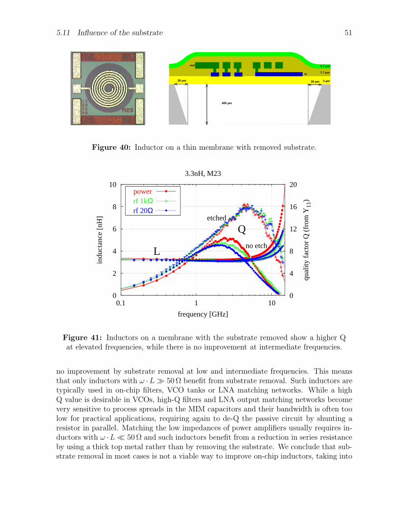
5.11 Influence of the substrate 51
Figure 40: Inductor on a thin membrane with removed substrate.
0
2
4
6
8
10
0.1 1 100
4
8
12
16
20
indu
ctan
ce [
nH]
qual
ity f
acto
r Q
(fr
om Y
11)
frequency [GHz]
3.3nH, M23
L
Qetched
no etch
powerrf 1kΩrf 20Ω
Figure 41: Inductors on a membrane with the substrate removed show a higher Qat elevated frequencies, while there is no improvement at intermediate frequencies.
no improvement by substrate removal at low and intermediate frequencies. This meansthat only inductors with ω ·L 50 Ω benefit from substrate removal. Such inductors aretypically used in on-chip filters, VCO tanks or LNA matching networks. While a highQ value is desirable in VCOs, high-Q filters and LNA output matching networks becomevery sensitive to process spreads in the MIM capacitors and their bandwidth is often toolow for practical applications, requiring again to de-Q the passive circuit by shunting aresistor in parallel. Matching the low impedances of power amplifiers usually requires in-ductors with ω ·L 50 Ω and such inductors benefit from a reduction in series resistanceby using a thick top metal rather than by removing the substrate. We conclude that sub-strate removal in most cases is not a viable way to improve on-chip inductors, taking into
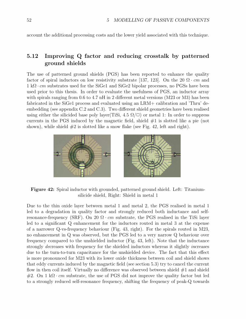
52 5 MODELLING OF PASSIVE COMPONENTS
account the additional processing costs and the lower yield associated with this technique.
5.12 Improving Q factor and reducing crosstalk by patternedground shields
The use of patterned ground shields (PGS) has been reported to enhance the qualityfactor of spiral inductors on low resistivity substrate [137, 123]. On the 20 Ω · cm and1 kΩ · cm substrates used for the SiGe1 and SiGe2 bipolar processes, no PGSs have beenused prior to this thesis. In order to evaluate the usefulness of PGS, an inductor arraywith spirals ranging from 0.6 to 4.7 nH in 2 different metal versions (M23 or M3) has beenfabricated in the SiGe1 process and evaluated using an LRM+ calibration and ’Thru’ de-embedding (see appendix C.2 and C.3). Two different shield geometries have been realisedusing either the silicided base poly layer(TiSi, 4.5 Ω/2) or metal 1: In order to suppresscurrents in the PGS induced by the magnetic field, shield #1 is slotted like a pie (notshown), while shield #2 is slotted like a snow flake (see Fig. 42, left and right).
Figure 42: Spiral inductor with grounded, patterned ground shield. Left: Titanium-silicide shield, Right: Shield in metal 1
Due to the thin oxide layer between metal 1 and metal 2, the PGS realised in metal 1led to a degradation in quality factor and strongly reduced both inductance and self-resonance-frequency (SRF). On 20 Ω · cm substrate, the PGS realised in the TiSi layerled to a significant Q enhancement for the inductors routed in metal 3 at the expenseof a narrower Q-vs-frequency behaviour (Fig. 43, right). For the spirals routed in M23,no enhancement in Q was observed, but the PGS led to a very narrow Q behaviour overfrequency compared to the unshielded inductor (Fig. 43, left). Note that the inductancestrongly decreases with frequency for the shielded inductors whereas it slightly increasesdue to the turn-to-turn capacitance for the unshielded device. The fact that this effectis more pronounced for M23 with its lower oxide thickness between coil and shield showsthat eddy currents induced by the magnetic field (see section 5.3) try to cancel the currentflow in then coil itself. Virtually no difference was observed between shield #1 and shield#2. On 1 kΩ · cm substrate, the use of PGS did not improve the quality factor but ledto a strongly reduced self-resonance frequency, shifting the frequency of peak-Q towards
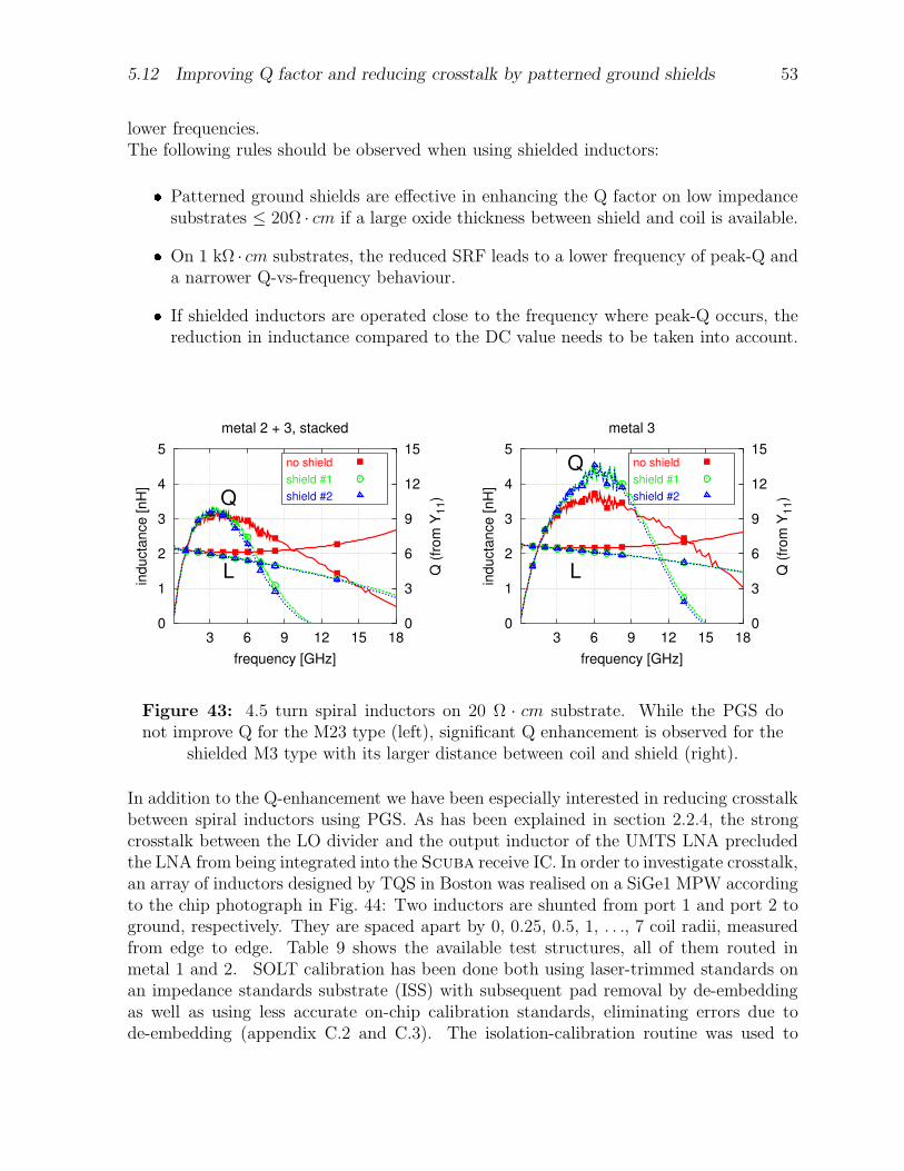
5.12 Improving Q factor and reducing crosstalk by patterned ground shields 53
lower frequencies.The following rules should be observed when using shielded inductors: Patterned ground shields are effective in enhancing the Q factor on low impedance
substrates ≤ 20Ω · cm if a large oxide thickness between shield and coil is available. On 1 kΩ · cm substrates, the reduced SRF leads to a lower frequency of peak-Q anda narrower Q-vs-frequency behaviour. If shielded inductors are operated close to the frequency where peak-Q occurs, thereduction in inductance compared to the DC value needs to be taken into account.
0
1
2
3
4
5
3 6 9 12 15 180
3
6
9
12
15
ind
ucta
nce
[n
H]
Q (
fro
m Y
11)
frequency [GHz]
metal 2 + 3, stacked
L
Q
no shield
shield #1
shield #2
0
1
2
3
4
5
3 6 9 12 15 180
3
6
9
12
15
ind
ucta
nce
[n
H]
Q (
fro
m Y
11)
frequency [GHz]
metal 3
L
Q no shield
shield #1
shield #2
Figure 43: 4.5 turn spiral inductors on 20 Ω · cm substrate. While the PGS donot improve Q for the M23 type (left), significant Q enhancement is observed for the
shielded M3 type with its larger distance between coil and shield (right).
In addition to the Q-enhancement we have been especially interested in reducing crosstalkbetween spiral inductors using PGS. As has been explained in section 2.2.4, the strongcrosstalk between the LO divider and the output inductor of the UMTS LNA precludedthe LNA from being integrated into the Scuba receive IC. In order to investigate crosstalk,an array of inductors designed by TQS in Boston was realised on a SiGe1 MPW accordingto the chip photograph in Fig. 44: Two inductors are shunted from port 1 and port 2 toground, respectively. They are spaced apart by 0, 0.25, 0.5, 1, . . ., 7 coil radii, measuredfrom edge to edge. Table 9 shows the available test structures, all of them routed inmetal 1 and 2. SOLT calibration has been done both using laser-trimmed standards onan impedance standards substrate (ISS) with subsequent pad removal by de-embeddingas well as using less accurate on-chip calibration standards, eliminating errors due tode-embedding (appendix C.2 and C.3). The isolation-calibration routine was used to
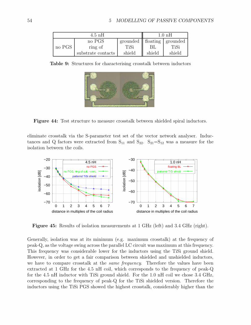
54 5 MODELLING OF PASSIVE COMPONENTS
4.5 nH 1.0 nHno PGS grounded floating grounded
no PGS ring of TiSi BL TiSisubstrate contacts shield shield shield
Table 9: Structures for characterising crosstalk between inductors
Figure 44: Test structure to measure crosstalk between shielded spiral inductors.
eliminate crosstalk via the S-parameter test set of the vector network analyser. Induc-tances and Q factors were extracted from S11 and S22. S21=S12 was a measure for theisolation between the coils.
−70
−60
−50
−40
−30
−20
0 1 2 3 4 5 6 7
isol
atio
n [d
B]
distance in multiples of the coil radius
4.5 nHno PGS
no PGS, ring of sub.−cont.
patternd TiSi shield
−70
−60
−50
−40
−30
0 1 2 3 4 5 6 7
isol
atio
n [d
B]
distance in multiples of the coil radius
1.0 nHfloating BL
patternd TiSi shield
Figure 45: Results of isolation measurements at 1 GHz (left) and 3.4 GHz (right).
Generally, isolation was at its minimum (e.g. maximum crosstalk) at the frequency ofpeak-Q, as the voltage swing across the parallel LC circuit was maximum at this frequency.This frequency was considerable lower for the inductors using the TiSi ground shield.However, in order to get a fair comparison between shielded and unshielded inductors,we have to compare crosstalk at the same frequency. Therefore the values have beenextracted at 1 GHz for the 4.5 nH coil, which corresponds to the frequency of peak-Qfor the 4.5 nH inductor with TiSi ground shield. For the 1.0 nH coil we chose 3.4 GHz,corresponding to the frequency of peak-Q for the TiSi shielded version. Therefore theinductors using the TiSi PGS showed the highest crosstalk, considerably higher than the
5.13 Electromagnetic field simulation 55
unshielded versions, which were operated considerably below the frequency of peak-Q.For large distances > 4× the coil-radius (measured from edge to edge), we found a 4 dBimprovement of the unshielded inductor with grounded ring of substrate contacts over theunshielded type, while there was virtually no effect at smaller distances. Peak-Q decreasesby approximately 10% using a ring of substrate contacts, however.
The following three guidelines can therefore be given:
1. Use a patterned ground shield to increase the peak-Q of inductors which are spacedapart far from the lossy substrate (M3-versions in the SiGe1 and SiGe2 technologies).Take care, as the frequency of peak-Q drops and there is a strong roll-off in Q athigher frequencies (see Fig. 43).
2. Use a ring of substrate contacts to reduce crosstalk between inductors which arespaced apart by more than 4 times the coil radii. However, depending on thedistance of substrate contact to the coil, the reduction in peak-Q is in the order of10% due to reduced values of Rsub (see Eqn. 25).
3. To reduce coupling between adjacent coils, there is not much that you can do.Incorporate this coupling into your simulation and try to make use of it.
4. As noted by Sonmez [145], using massive metal planes with defined spacing aroundthe inductors leads to a better reproducibility for layouts at high frequencies (e.g.24 GHz) at the expense of reduced inductance due to the eddy currents induced inthe metal planes.
It is interesting to note that both the inductance and the quality factor of the individualinductors increase slightly when the distance between them decreases. This points toa constructive coupling process and motivates the investigations towards symmetricalinductors in section 5.17.
5.13 Electromagnetic field simulation
5.13.1 2.5D simulators based on the method of moments
At the beginning of this thesis, no EM based software tools have been available thatsimulate inductors on lossy substrates, including metallisation loss, in short time on afast PC or workstation with sufficient accuracy. Just at the end of this work, the toolshave been powerful enough to model inductance and Q-factor accurately. Therefore,within the framework of this thesis, several 2.5D simulators and one 3D simulators havebeen investigated:All of the 2.5D simulators used were based on the Method of Moments (MoM), which datesback to the work of R.F. Harrington in 1960. It is a numerical discretization techniquewhich solves Maxwell’s equations for planar conductors (with zero thickness) embedded
56 5 MODELLING OF PASSIVE COMPONENTS
in a multi-layered dielectric substrate. The term 2.5D means that current in the planeperpendicular to the conducting XY layers can only flow in Z-direction, no current flowin ZX or ZY directions can be taken into account. Extensive evaluation was done on two2.5D commercial tools, which differ in the way they solve these equations: The Momentum simulator, included in Agilent technologies’ Advanced Design Sys-
tem, relies on a 4-dimensional numerical integration technique to calculate eachpair-wise coupling between the mesh elements [146]. Sonnet from Sonnet Software, Inc. utilises the so-called closed-box solution inconjunction with a uniform grid which is solved using an FFT-based analysis [147].
Both Momentum and Sonnet introduced an intelligent frequency interpolation algorithm(called adaptive frequency sweep, AFS in Sonnet), which fitted the S-parameters of thecomplete frequency range to just a few EM simulated frequency points, greatly enhancingsimulation speed. The term ’intelligent’ means that the software autonomously decidedwhere to set the simulation frequencies within frequency range selected by the user. Thisfeature greatly speeds up the simulation process and it is amazing, how even narrow-bandfilters with several poles can be simulated with just 5–8 frequency points. For spiralinductors, however, this feature had to be used with caution: The software stopped theprocess of setting and simulating additional stilt frequency points, when the differencebetween the actually simulated result at a given frequency compared to the intelligent fitwas smaller than a given ∆. While this works excellently for the inductance of a spiralinductor, large errors and even severe discontinuities of the Q-factor in the frequencyrange of peak-Q occurred! Therefore, in addition to the frequencies set by AFS auto-matically, the simulator had to be forced to simulate several additional frequencies in theregion of peak-Q. The reason is the strong dependence of Q on the slightest changes inS-parameters and was explained already earlier in section 5.5. This makes the qualityfactor of a spiral both difficult to measure (influence of contact resistance, on-wafer cali-bration, de-embedding, see section C) and difficult to simulate.
5.13.2 Why a planar inductor is not a two-dimensional structure
Using the 2.5 D simulator, numerous simulations have shown that there was initially abig difference in both inductance and Q-factor between measured and simulated results:
1. The Q-factor always simulated too high compared to the measurements, a fact thatfirst was attributed to poor measurements conditions (e.g. contact resistance) or toa degradation in substrate resistivity during wafer fabrication or to a metal thicknesswhich could be thinner than specified.
2. The inductance always simulated too high. This was initially attributed to poorde-embedding.
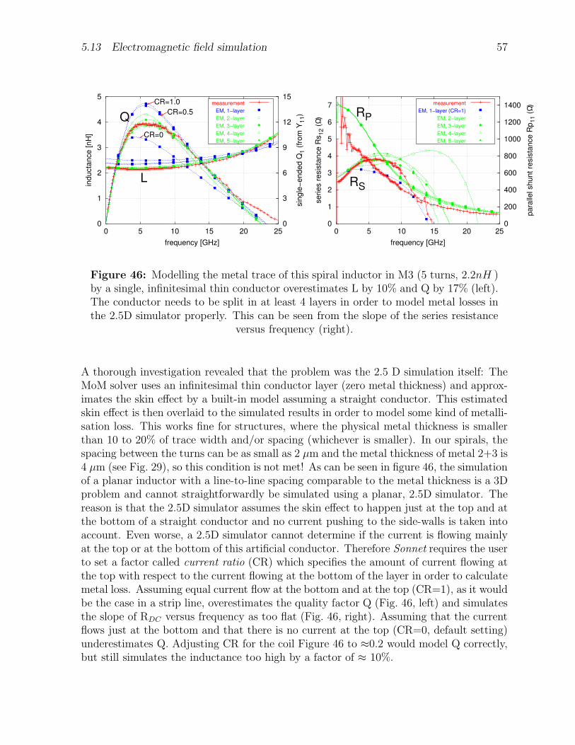
5.13 Electromagnetic field simulation 57
0
1
2
3
4
5
0 5 10 15 20 250
3
6
9
12
15in
ducta
nce [nH
]
sin
gle
−ended Q
1 (
from
Y11)
frequency [GHz]
L
Q
CR=1.0
CR=0.5
CR=0
measurement
EM, 1−layer
EM, 2−layer
EM, 3−layer
EM, 4−layer
EM, 5−layer
0
1
2
3
4
5
6
7
0 5 10 15 20 250
200
400
600
800
1000
1200
1400
series r
esis
tance R
s12 (
Ω)
para
llel shunt re
sis
tance R
p11 (
Ω)
frequency [GHz]
RS
RP
measurement
EM, 1−layer (CR=1)
EM, 2−layer
EM, 3−layer
EM, 4−layer
EM, 5−layer
Figure 46: Modelling the metal trace of this spiral inductor in M3 (5 turns, 2.2nH )by a single, infinitesimal thin conductor overestimates L by 10% and Q by 17% (left).The conductor needs to be split in at least 4 layers in order to model metal losses inthe 2.5D simulator properly. This can be seen from the slope of the series resistance
versus frequency (right).
A thorough investigation revealed that the problem was the 2.5 D simulation itself: TheMoM solver uses an infinitesimal thin conductor layer (zero metal thickness) and approx-imates the skin effect by a built-in model assuming a straight conductor. This estimatedskin effect is then overlaid to the simulated results in order to model some kind of metalli-sation loss. This works fine for structures, where the physical metal thickness is smallerthan 10 to 20% of trace width and/or spacing (whichever is smaller). In our spirals, thespacing between the turns can be as small as 2 µm and the metal thickness of metal 2+3 is4 µm (see Fig. 29), so this condition is not met! As can be seen in figure 46, the simulationof a planar inductor with a line-to-line spacing comparable to the metal thickness is a 3Dproblem and cannot straightforwardly be simulated using a planar, 2.5D simulator. Thereason is that the 2.5D simulator assumes the skin effect to happen just at the top and atthe bottom of a straight conductor and no current pushing to the side-walls is taken intoaccount. Even worse, a 2.5D simulator cannot determine if the current is flowing mainlyat the top or at the bottom of this artificial conductor. Therefore Sonnet requires the userto set a factor called current ratio (CR) which specifies the amount of current flowing atthe top with respect to the current flowing at the bottom of the layer in order to calculatemetal loss. Assuming equal current flow at the bottom and at the top (CR=1), as it wouldbe the case in a strip line, overestimates the quality factor Q (Fig. 46, left) and simulatesthe slope of RDC versus frequency as too flat (Fig. 46, right). Assuming that the currentflows just at the bottom and that there is no current at the top (CR=0, default setting)underestimates Q. Adjusting CR for the coil Figure 46 to ≈0.2 would model Q correctly,but still simulates the inductance too high by a factor of ≈ 10%.
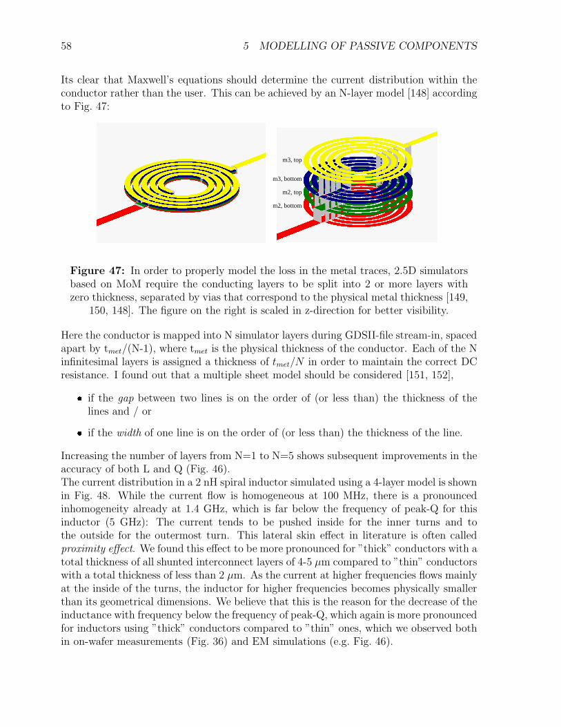
58 5 MODELLING OF PASSIVE COMPONENTS
Its clear that Maxwell’s equations should determine the current distribution within theconductor rather than the user. This can be achieved by an N-layer model [148] accordingto Fig. 47:
m3, top
m2, bottom
m3, bottom
m2, top
Figure 47: In order to properly model the loss in the metal traces, 2.5D simulatorsbased on MoM require the conducting layers to be split into 2 or more layers withzero thickness, separated by vias that correspond to the physical metal thickness [149,
150, 148]. The figure on the right is scaled in z-direction for better visibility.
Here the conductor is mapped into N simulator layers during GDSII-file stream-in, spacedapart by tmet/(N-1), where tmet is the physical thickness of the conductor. Each of the Ninfinitesimal layers is assigned a thickness of tmet/N in order to maintain the correct DCresistance. I found out that a multiple sheet model should be considered [151, 152], if the gap between two lines is on the order of (or less than) the thickness of the
lines and / or if the width of one line is on the order of (or less than) the thickness of the line.
Increasing the number of layers from N=1 to N=5 shows subsequent improvements in theaccuracy of both L and Q (Fig. 46).The current distribution in a 2 nH spiral inductor simulated using a 4-layer model is shownin Fig. 48. While the current flow is homogeneous at 100 MHz, there is a pronouncedinhomogeneity already at 1.4 GHz, which is far below the frequency of peak-Q for thisinductor (5 GHz): The current tends to be pushed inside for the inner turns and tothe outside for the outermost turn. This lateral skin effect in literature is often calledproximity effect. We found this effect to be more pronounced for ”thick” conductors with atotal thickness of all shunted interconnect layers of 4-5 µm compared to ”thin” conductorswith a total thickness of less than 2 µm. As the current at higher frequencies flows mainlyat the inside of the turns, the inductor for higher frequencies becomes physically smallerthan its geometrical dimensions. We believe that this is the reason for the decrease of theinductance with frequency below the frequency of peak-Q, which again is more pronouncedfor inductors using ”thick” conductors compared to ”thin” ones, which we observed bothin on-wafer measurements (Fig. 36) and EM simulations (e.g. Fig. 46).
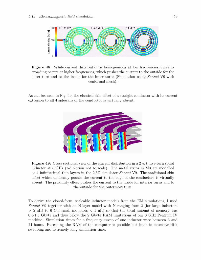
5.13 Electromagnetic field simulation 59
7 GHz10 MHz 1.4 GHz
500
curr
ent d
ensi
ty [
A/m
]
900
0
Figure 48: While current distribution is homogeneous at low frequencies, current-crowding occurs at higher frequencies, which pushes the current to the outside for theouter turn and to the inside for the inner turns (Simulation using Sonnet V9 with
conformal mesh).
As can bee seen in Fig. 49, the classical skin effect of a straight conductor with its currentextrusion to all 4 sidewalls of the conductor is virtually absent.
Figure 49: Cross sectional view of the current distribution in a 2 nH , five-turn spiralinductor at 5 GHz (z-direction not to scale). The metal strips in M3 are modelledas 4 infinitesimal thin layers in the 2.5D simulator Sonnet V9. The traditional skineffect which uniformly pushes the current to the edge of the conductors is virtuallyabsent. The proximity effect pushes the current to the inside for interior turns and to
the outside for the outermost turn.
To derive the closed-form, scaleable inductor models from the EM simulations, I usedSonnet V9 together with an N-layer model with N ranging from 2 (for large inductors> 5 nH) to 6 (for small inductors < 1 nH) so that the total amount of memory was0.5-1.5 Gbyte and thus below the 2 Gbyte RAM limitations of our 3 GHz Pentium IVmachine. Simulation times for a frequency sweep of one inductor were between 3 and24 hours. Exceeding the RAM of the computer is possible but leads to extensive diskswapping and extremely long simulation time.
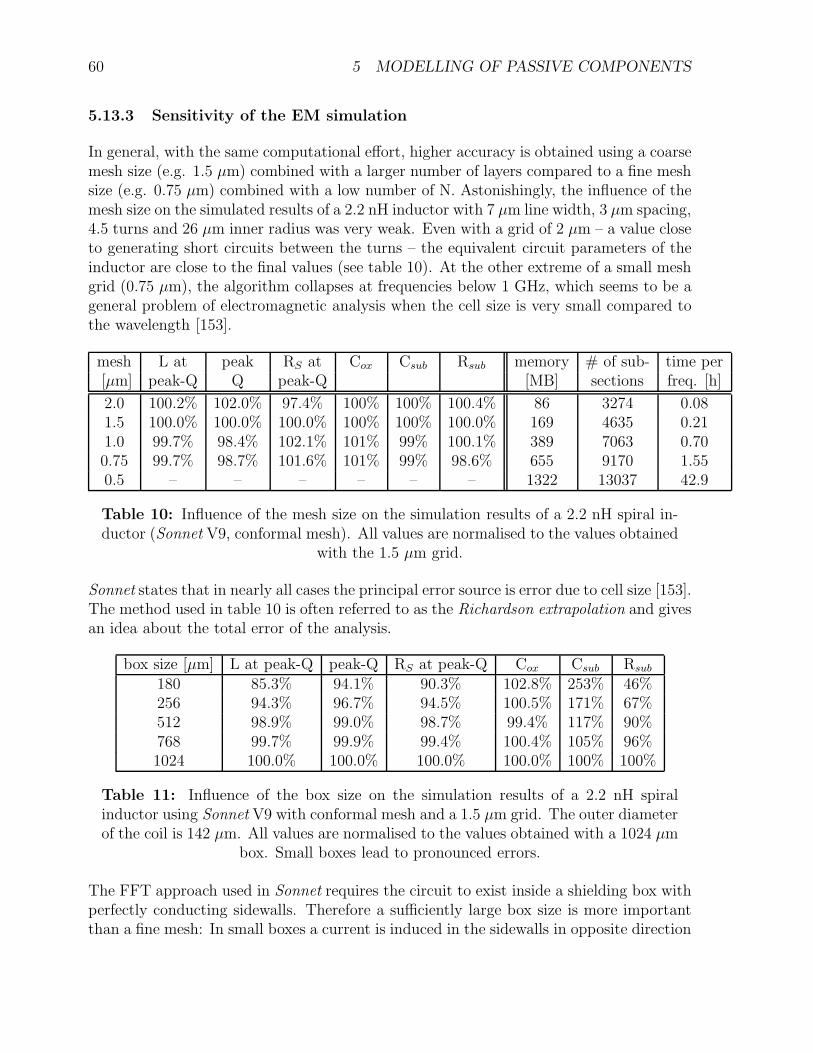
60 5 MODELLING OF PASSIVE COMPONENTS
5.13.3 Sensitivity of the EM simulation
In general, with the same computational effort, higher accuracy is obtained using a coarsemesh size (e.g. 1.5 µm) combined with a larger number of layers compared to a fine meshsize (e.g. 0.75 µm) combined with a low number of N. Astonishingly, the influence of themesh size on the simulated results of a 2.2 nH inductor with 7 µm line width, 3 µm spacing,4.5 turns and 26 µm inner radius was very weak. Even with a grid of 2 µm – a value closeto generating short circuits between the turns – the equivalent circuit parameters of theinductor are close to the final values (see table 10). At the other extreme of a small meshgrid (0.75 µm), the algorithm collapses at frequencies below 1 GHz, which seems to be ageneral problem of electromagnetic analysis when the cell size is very small compared tothe wavelength [153].
mesh L at peak RS at Cox Csub Rsub memory # of sub- time per[µm] peak-Q Q peak-Q [MB] sections freq. [h]
2.0 100.2% 102.0% 97.4% 100% 100% 100.4% 86 3274 0.081.5 100.0% 100.0% 100.0% 100% 100% 100.0% 169 4635 0.211.0 99.7% 98.4% 102.1% 101% 99% 100.1% 389 7063 0.700.75 99.7% 98.7% 101.6% 101% 99% 98.6% 655 9170 1.550.5 – – – – – – 1322 13037 42.9
Table 10: Influence of the mesh size on the simulation results of a 2.2 nH spiral in-ductor (Sonnet V9, conformal mesh). All values are normalised to the values obtained
with the 1.5 µm grid.
Sonnet states that in nearly all cases the principal error source is error due to cell size [153].The method used in table 10 is often referred to as the Richardson extrapolation and givesan idea about the total error of the analysis.
box size [µm] L at peak-Q peak-Q RS at peak-Q Cox Csub Rsub
180 85.3% 94.1% 90.3% 102.8% 253% 46%256 94.3% 96.7% 94.5% 100.5% 171% 67%512 98.9% 99.0% 98.7% 99.4% 117% 90%768 99.7% 99.9% 99.4% 100.4% 105% 96%1024 100.0% 100.0% 100.0% 100.0% 100% 100%
Table 11: Influence of the box size on the simulation results of a 2.2 nH spiralinductor using Sonnet V9 with conformal mesh and a 1.5 µm grid. The outer diameterof the coil is 142 µm. All values are normalised to the values obtained with a 1024 µm
box. Small boxes lead to pronounced errors.
The FFT approach used in Sonnet requires the circuit to exist inside a shielding box withperfectly conducting sidewalls. Therefore a sufficiently large box size is more importantthan a fine mesh: In small boxes a current is induced in the sidewalls in opposite direction
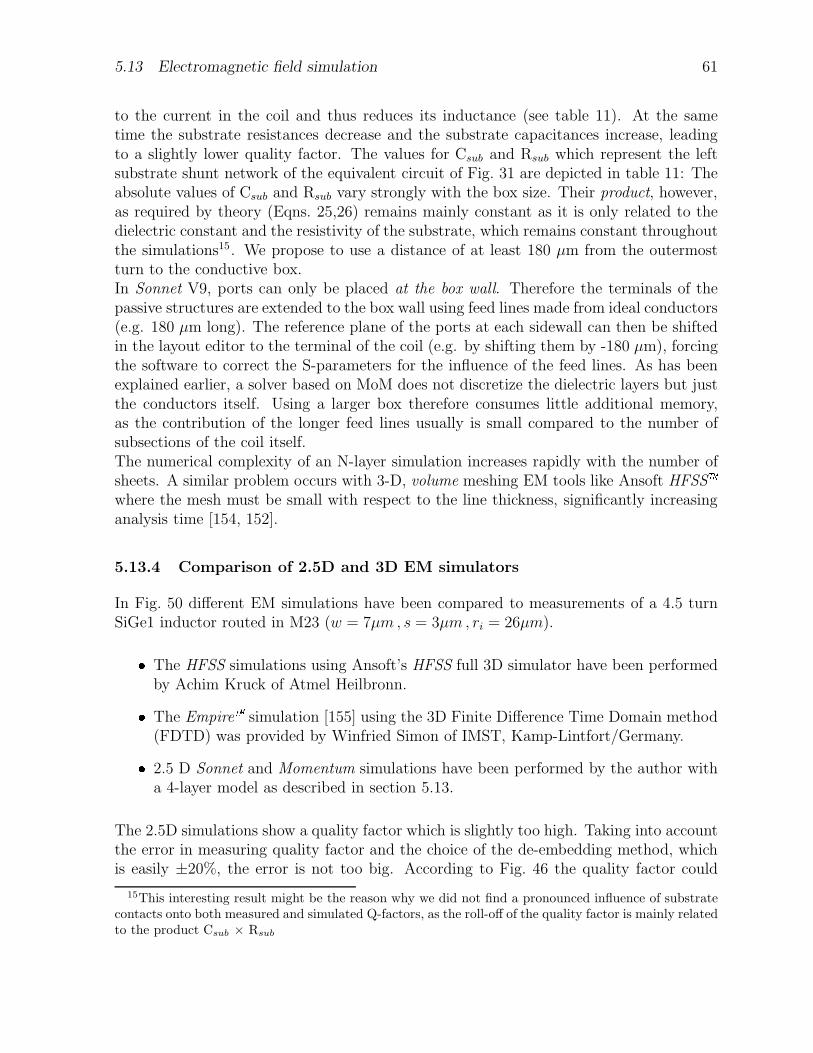
5.13 Electromagnetic field simulation 61
to the current in the coil and thus reduces its inductance (see table 11). At the sametime the substrate resistances decrease and the substrate capacitances increase, leadingto a slightly lower quality factor. The values for Csub and Rsub which represent the leftsubstrate shunt network of the equivalent circuit of Fig. 31 are depicted in table 11: Theabsolute values of Csub and Rsub vary strongly with the box size. Their product, however,as required by theory (Eqns. 25,26) remains mainly constant as it is only related to thedielectric constant and the resistivity of the substrate, which remains constant throughoutthe simulations15. We propose to use a distance of at least 180 µm from the outermostturn to the conductive box.In Sonnet V9, ports can only be placed at the box wall. Therefore the terminals of thepassive structures are extended to the box wall using feed lines made from ideal conductors(e.g. 180 µm long). The reference plane of the ports at each sidewall can then be shiftedin the layout editor to the terminal of the coil (e.g. by shifting them by -180 µm), forcingthe software to correct the S-parameters for the influence of the feed lines. As has beenexplained earlier, a solver based on MoM does not discretize the dielectric layers but justthe conductors itself. Using a larger box therefore consumes little additional memory,as the contribution of the longer feed lines usually is small compared to the number ofsubsections of the coil itself.The numerical complexity of an N-layer simulation increases rapidly with the number ofsheets. A similar problem occurs with 3-D, volume meshing EM tools like Ansoft HFSSwhere the mesh must be small with respect to the line thickness, significantly increasinganalysis time [154, 152].
5.13.4 Comparison of 2.5D and 3D EM simulators
In Fig. 50 different EM simulations have been compared to measurements of a 4.5 turnSiGe1 inductor routed in M23 (w = 7µm , s = 3µm , ri = 26µm). The HFSS simulations using Ansoft’s HFSS full 3D simulator have been performed
by Achim Kruck of Atmel Heilbronn. The Empire simulation [155] using the 3D Finite Difference Time Domain method(FDTD) was provided by Winfried Simon of IMST, Kamp-Lintfort/Germany. 2.5 D Sonnet and Momentum simulations have been performed by the author witha 4-layer model as described in section 5.13.
The 2.5D simulations show a quality factor which is slightly too high. Taking into accountthe error in measuring quality factor and the choice of the de-embedding method, whichis easily ±20%, the error is not too big. According to Fig. 46 the quality factor could
15This interesting result might be the reason why we did not find a pronounced influence of substratecontacts onto both measured and simulated Q-factors, as the roll-off of the quality factor is mainly relatedto the product Csub × Rsub
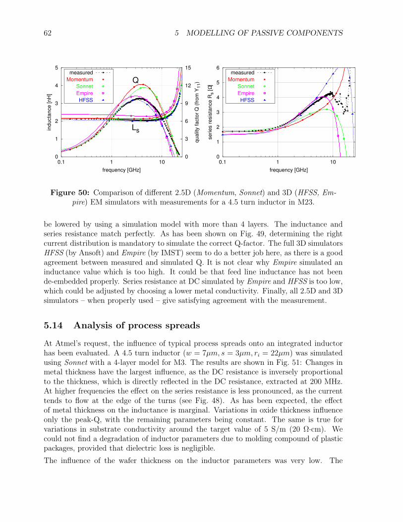
62 5 MODELLING OF PASSIVE COMPONENTS
0
1
2
3
4
5
0.1 1 100
3
6
9
12
15
inducta
nce [nH
]
qualit
y facto
r Q
(fr
om
Y11)
frequency [GHz]
Q
Ls
measured
Momentum
Sonnet
Empire
HFSS
0
1
2
3
4
5
6
0.1 1 10
series r
esis
tance R
s [
Ω]
frequency [GHz]
measured
Momentum
Sonnet
Empire
HFSS
Figure 50: Comparison of different 2.5D (Momentum, Sonnet) and 3D (HFSS, Em-pire) EM simulators with measurements for a 4.5 turn inductor in M23.
be lowered by using a simulation model with more than 4 layers. The inductance andseries resistance match perfectly. As has been shown on Fig. 49, determining the rightcurrent distribution is mandatory to simulate the correct Q-factor. The full 3D simulatorsHFSS (by Ansoft) and Empire (by IMST) seem to do a better job here, as there is a goodagreement between measured and simulated Q. It is not clear why Empire simulated aninductance value which is too high. It could be that feed line inductance has not beende-embedded properly. Series resistance at DC simulated by Empire and HFSS is too low,which could be adjusted by choosing a lower metal conductivity. Finally, all 2.5D and 3Dsimulators – when properly used – give satisfying agreement with the measurement.
5.14 Analysis of process spreads
At Atmel’s request, the influence of typical process spreads onto an integrated inductorhas been evaluated. A 4.5 turn inductor (w = 7µm, s = 3µm, ri = 22µm) was simulatedusing Sonnet with a 4-layer model for M3. The results are shown in Fig. 51: Changes inmetal thickness have the largest influence, as the DC resistance is inversely proportionalto the thickness, which is directly reflected in the DC resistance, extracted at 200 MHz.At higher frequencies the effect on the series resistance is less pronounced, as the currenttends to flow at the edge of the turns (see Fig. 48). As has been expected, the effectof metal thickness on the inductance is marginal. Variations in oxide thickness influenceonly the peak-Q, with the remaining parameters being constant. The same is true forvariations in substrate conductivity around the target value of 5 S/m (20 Ω·cm). Wecould not find a degradation of inductor parameters due to molding compound of plasticpackages, provided that dielectric loss is negligible.
The influence of the wafer thickness on the inductor parameters was very low. The
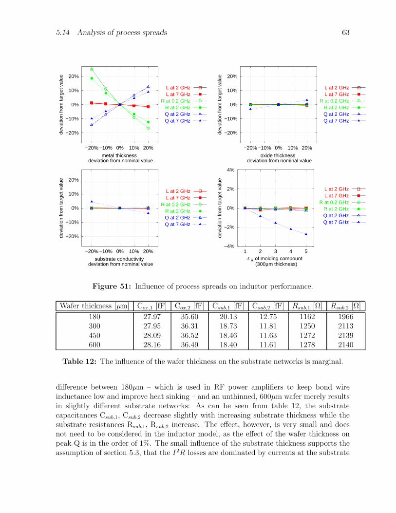
5.14 Analysis of process spreads 63
−20%
−10%
0%
10%
20%
−20% −10% 0% 10% 20%
devi
atio
n fr
om ta
rget
val
ue
metal thickness deviation from nominal value
L at 2 GHzL at 7 GHz
R at 0.2 GHzR at 2 GHzQ at 2 GHzQ at 7 GHz
−20%
−10%
0%
10%
20%
−20% −10% 0% 10% 20%
devi
atio
n fr
om ta
rget
val
ue
oxide thickness deviation from nominal value
L at 2 GHzL at 7 GHz
R at 0.2 GHzR at 2 GHzQ at 2 GHzQ at 7 GHz
−20%
−10%
0%
10%
20%
−20% −10% 0% 10% 20%
devi
atio
n fr
om ta
rget
val
ue
substrate conductivity deviation from nominal value
L at 2 GHzL at 7 GHz
R at 0.2 GHzR at 2 GHzQ at 2 GHzQ at 7 GHz
−4%
−2%
0%
2%
4%
1 2 3 4 5
devi
atio
n fr
om ta
rget
val
ue
ε R of molding compount (300µm thickness)
L at 2 GHzL at 7 GHz
R at 0.2 GHzR at 2 GHzQ at 2 GHzQ at 7 GHz
Figure 51: Influence of process spreads on inductor performance.
Wafer thickness [µm] Cox,1 [fF] Cox,2 [fF] Csub,1 [fF] Csub,2 [fF] Rsub,1 [Ω] Rsub,2 [Ω]
180 27.97 35.60 20.13 12.75 1162 1966300 27.95 36.31 18.73 11.81 1250 2113450 28.09 36.52 18.46 11.63 1272 2139600 28.16 36.49 18.40 11.61 1278 2140
Table 12: The influence of the wafer thickness on the substrate networks is marginal.
difference between 180µm – which is used in RF power amplifiers to keep bond wireinductance low and improve heat sinking – and an unthinned, 600µm wafer merely resultsin slightly different substrate networks: As can be seen from table 12, the substratecapacitances Csub,1, Csub,2 decrease slightly with increasing substrate thickness while thesubstrate resistances Rsub,1, Rsub,2 increase. The effect, however, is very small and doesnot need to be considered in the inductor model, as the effect of the wafer thickness onpeak-Q is in the order of 1%. The small influence of the substrate thickness supports theassumption of section 5.3, that the I2R losses are dominated by currents at the substrate
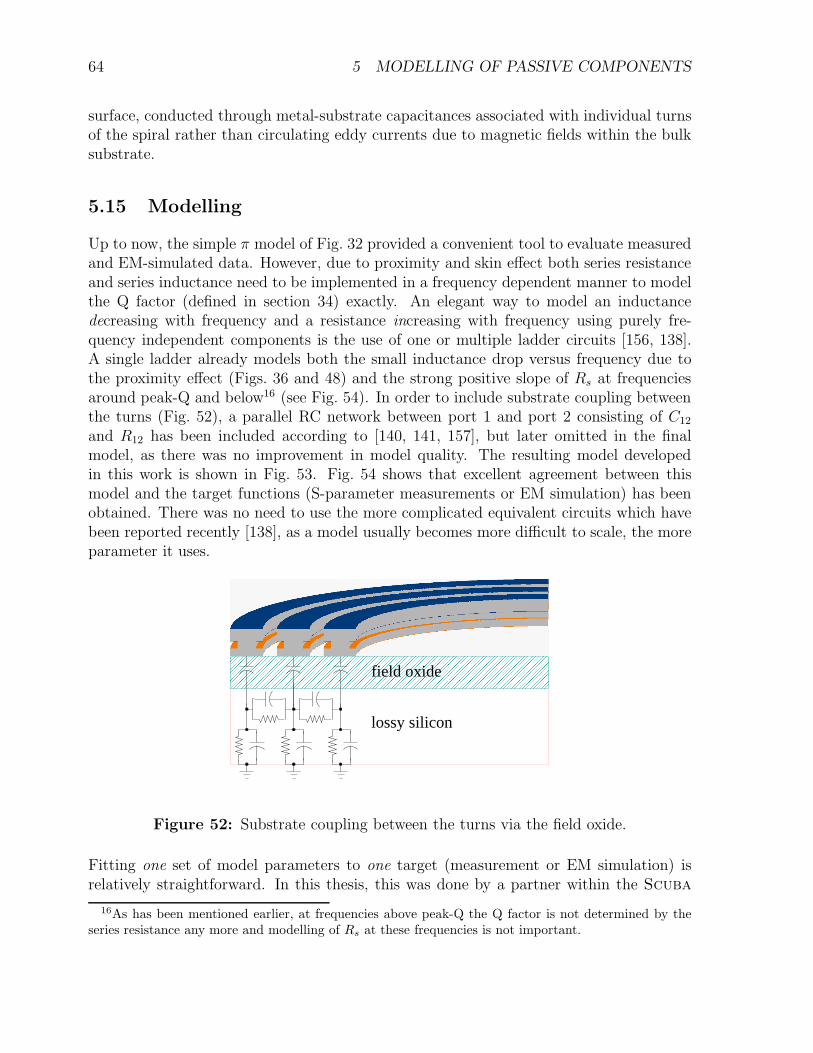
64 5 MODELLING OF PASSIVE COMPONENTS
surface, conducted through metal-substrate capacitances associated with individual turnsof the spiral rather than circulating eddy currents due to magnetic fields within the bulksubstrate.
5.15 Modelling
Up to now, the simple π model of Fig. 32 provided a convenient tool to evaluate measuredand EM-simulated data. However, due to proximity and skin effect both series resistanceand series inductance need to be implemented in a frequency dependent manner to modelthe Q factor (defined in section 34) exactly. An elegant way to model an inductancedecreasing with frequency and a resistance increasing with frequency using purely fre-quency independent components is the use of one or multiple ladder circuits [156, 138].A single ladder already models both the small inductance drop versus frequency due tothe proximity effect (Figs. 36 and 48) and the strong positive slope of Rs at frequenciesaround peak-Q and below16 (see Fig. 54). In order to include substrate coupling betweenthe turns (Fig. 52), a parallel RC network between port 1 and port 2 consisting of C12
and R12 has been included according to [140, 141, 157], but later omitted in the finalmodel, as there was no improvement in model quality. The resulting model developedin this work is shown in Fig. 53. Fig. 54 shows that excellent agreement between thismodel and the target functions (S-parameter measurements or EM simulation) has beenobtained. There was no need to use the more complicated equivalent circuits which havebeen reported recently [138], as a model usually becomes more difficult to scale, the moreparameter it uses.
lossy silicon
field oxide
Figure 52: Substrate coupling between the turns via the field oxide.
Fitting one set of model parameters to one target (measurement or EM simulation) isrelatively straightforward. In this thesis, this was done by a partner within the Scuba
16As has been mentioned earlier, at frequencies above peak-Q the Q factor is not determined by theseries resistance any more and modelling of Rs at these frequencies is not important.
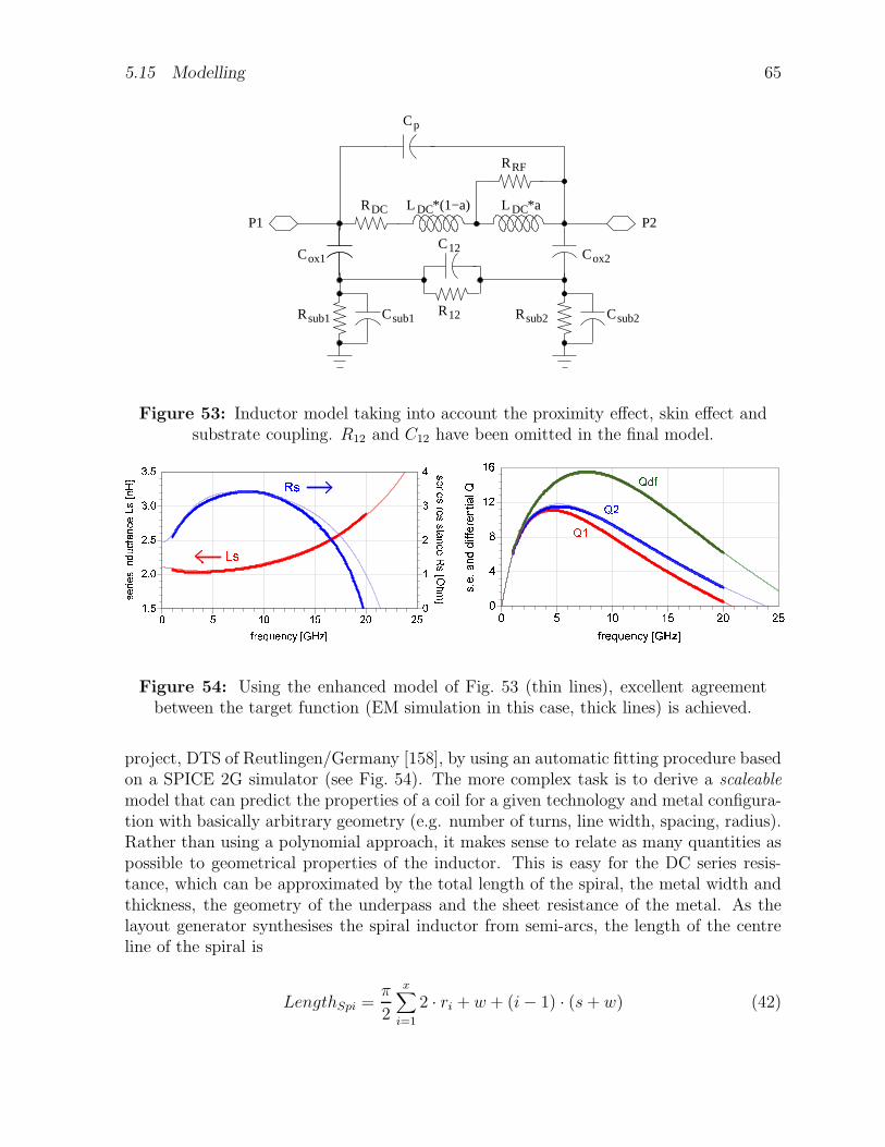
5.15 Modelling 65
ox1C
DCR
sub1R sub1C sub2R sub2C
12C
12R
ox2C
DCL *(1−a) DCL *a
RFR
pC
P1 P2
Figure 53: Inductor model taking into account the proximity effect, skin effect andsubstrate coupling. R12 and C12 have been omitted in the final model.
Figure 54: Using the enhanced model of Fig. 53 (thin lines), excellent agreementbetween the target function (EM simulation in this case, thick lines) is achieved.
project, DTS of Reutlingen/Germany [158], by using an automatic fitting procedure basedon a SPICE 2G simulator (see Fig. 54). The more complex task is to derive a scaleablemodel that can predict the properties of a coil for a given technology and metal configura-tion with basically arbitrary geometry (e.g. number of turns, line width, spacing, radius).Rather than using a polynomial approach, it makes sense to relate as many quantities aspossible to geometrical properties of the inductor. This is easy for the DC series resis-tance, which can be approximated by the total length of the spiral, the metal width andthickness, the geometry of the underpass and the sheet resistance of the metal. As thelayout generator synthesises the spiral inductor from semi-arcs, the length of the centreline of the spiral is
LengthSpi =π
2
x∑
i=1
2 · ri + w + (i − 1) · (s + w) (42)
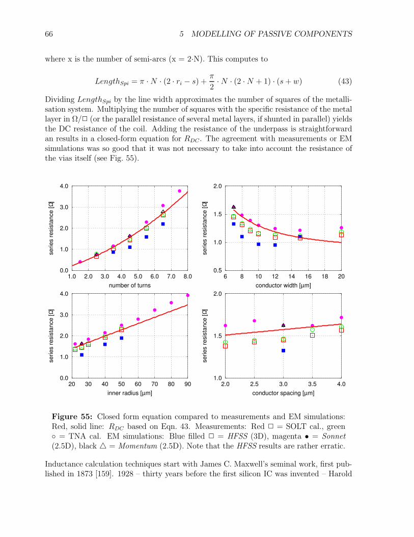
66 5 MODELLING OF PASSIVE COMPONENTS
where x is the number of semi-arcs (x = 2·N). This computes to
LengthSpi = π · N · (2 · ri − s) +π
2· N · (2 · N + 1) · (s + w) (43)
Dividing LengthSpi by the line width approximates the number of squares of the metalli-sation system. Multiplying the number of squares with the specific resistance of the metallayer in Ω/2 (or the parallel resistance of several metal layers, if shunted in parallel) yieldsthe DC resistance of the coil. Adding the resistance of the underpass is straightforwardan results in a closed-form equation for RDC . The agreement with measurements or EMsimulations was so good that it was not necessary to take into account the resistance ofthe vias itself (see Fig. 55).
0.5
1.0
1.5
2.0
6 8 10 12 14 16 18 20
series r
esis
tance [
Ω]
conductor width [µm]
0.0
1.0
2.0
3.0
4.0
1.0 2.0 3.0 4.0 5.0 6.0 7.0 8.0
series r
esis
tance [
Ω]
number of turns
0.0
1.0
2.0
3.0
4.0
20 30 40 50 60 70 80 90
series r
esis
tance [
Ω]
inner radius [µm]
1.0
1.5
2.0
2.0 2.5 3.0 3.5 4.0
series r
esis
tance [
Ω]
conductor spacing [µm]
Figure 55: Closed form equation compared to measurements and EM simulations:Red, solid line: RDC based on Eqn. 43. Measurements: Red 2 = SOLT cal., green = TNA cal. EM simulations: Blue filled 2 = HFSS (3D), magenta • = Sonnet(2.5D), black 4 = Momentum (2.5D). Note that the HFSS results are rather erratic.
Inductance calculation techniques start with James C. Maxwell’s seminal work, first pub-lished in 1873 [159]. 1928 – thirty years before the first silicon IC was invented – Harold
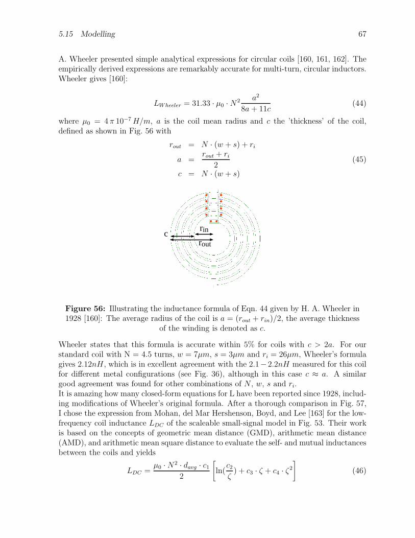
5.15 Modelling 67
A. Wheeler presented simple analytical expressions for circular coils [160, 161, 162]. Theempirically derived expressions are remarkably accurate for multi-turn, circular inductors.Wheeler gives [160]:
LWheeler = 31.33 · µ0 · N2 a2
8a + 11c(44)
where µ0 = 4 π 10−7 H/m, a is the coil mean radius and c the ’thickness’ of the coil,defined as shown in Fig. 56 with
rout = N · (w + s) + ri
a =rout + ri
2(45)
c = N · (w + s)
rout
rinc
Figure 56: Illustrating the inductance formula of Eqn. 44 given by H. A. Wheeler in1928 [160]: The average radius of the coil is a = (rout + rin)/2, the average thickness
of the winding is denoted as c.
Wheeler states that this formula is accurate within 5% for coils with c > 2a. For ourstandard coil with N = 4.5 turns, w = 7µm, s = 3µm and ri = 26µm, Wheeler’s formulagives 2.12nH , which is in excellent agreement with the 2.1−2.2nH measured for this coilfor different metal configurations (see Fig. 36), although in this case c ≈ a. A similargood agreement was found for other combinations of N , w, s and ri.It is amazing how many closed-form equations for L have been reported since 1928, includ-ing modifications of Wheeler’s original formula. After a thorough comparison in Fig. 57,I chose the expression from Mohan, del Mar Hershenson, Boyd, and Lee [163] for the low-frequency coil inductance LDC of the scaleable small-signal model in Fig. 53. Their workis based on the concepts of geometric mean distance (GMD), arithmetic mean distance(AMD), and arithmetic mean square distance to evaluate the self- and mutual inductancesbetween the coils and yields
LDC =µ0 · N2 · davg · c1
2
[
ln(c2
ζ) + c3 · ζ + c4 · ζ2
]
(46)
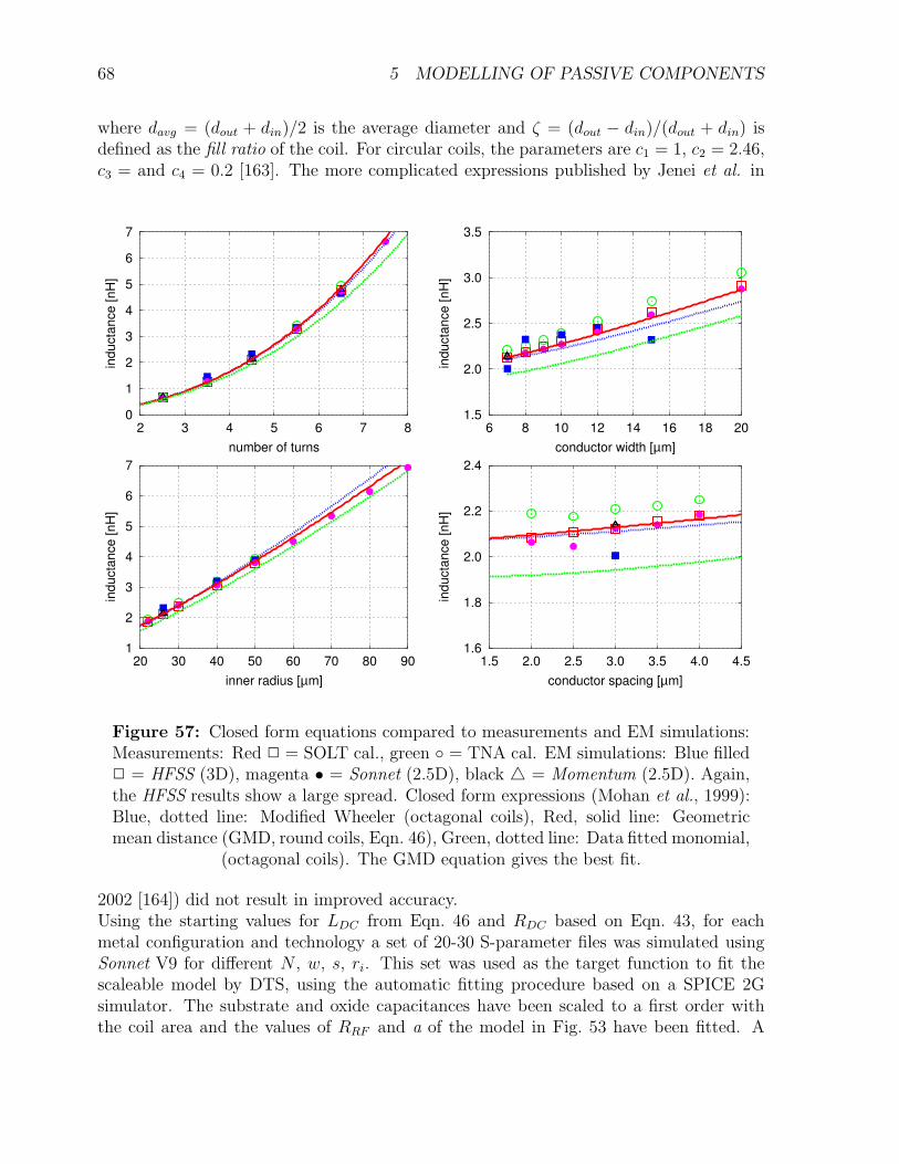
68 5 MODELLING OF PASSIVE COMPONENTS
where davg = (dout + din)/2 is the average diameter and ζ = (dout − din)/(dout + din) isdefined as the fill ratio of the coil. For circular coils, the parameters are c1 = 1, c2 = 2.46,c3 = and c4 = 0.2 [163]. The more complicated expressions published by Jenei et al. in
1.5
2.0
2.5
3.0
3.5
6 8 10 12 14 16 18 20
inducta
nce [nH
]conductor width [µm]
0
1
2
3
4
5
6
7
2 3 4 5 6 7 8
inducta
nce [nH
]
number of turns
1
2
3
4
5
6
7
20 30 40 50 60 70 80 90
inducta
nce [nH
]
inner radius [µm]
1.6
1.8
2.0
2.2
2.4
1.5 2.0 2.5 3.0 3.5 4.0 4.5
inducta
nce [nH
]
conductor spacing [µm]
Figure 57: Closed form equations compared to measurements and EM simulations:Measurements: Red 2 = SOLT cal., green = TNA cal. EM simulations: Blue filled2 = HFSS (3D), magenta • = Sonnet (2.5D), black 4 = Momentum (2.5D). Again,the HFSS results show a large spread. Closed form expressions (Mohan et al., 1999):Blue, dotted line: Modified Wheeler (octagonal coils), Red, solid line: Geometricmean distance (GMD, round coils, Eqn. 46), Green, dotted line: Data fitted monomial,
(octagonal coils). The GMD equation gives the best fit.
2002 [164]) did not result in improved accuracy.Using the starting values for LDC from Eqn. 46 and RDC based on Eqn. 43, for eachmetal configuration and technology a set of 20-30 S-parameter files was simulated usingSonnet V9 for different N , w, s, ri. This set was used as the target function to fit thescaleable model by DTS, using the automatic fitting procedure based on a SPICE 2Gsimulator. The substrate and oxide capacitances have been scaled to a first order withthe coil area and the values of RRF and a of the model in Fig. 53 have been fitted. A
5.15 Modelling 69
detailed explanation is beyond this work and the reader is therefore referred to [158].The models itself have been implemented in the design kits of the technologies, greatlyimproving the agreement between measurements and circuit design (see e.g. Fig. 88 inchapter 6).As shown in appendix F, a software tool has been developed based on empirical formulaethat – for a given inductance operating frequency – calculates all possible coil combinationsand sorts them for the highest Q factor or the lowest outer diameter (see Fig. 155).
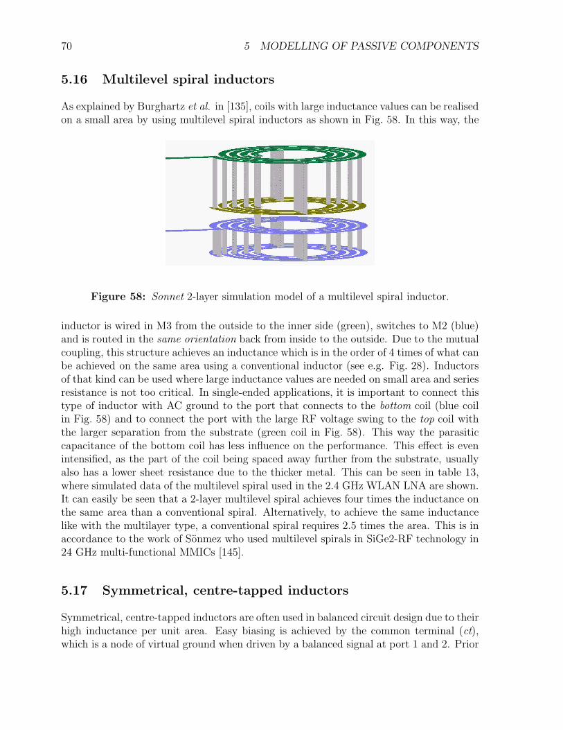
70 5 MODELLING OF PASSIVE COMPONENTS
5.16 Multilevel spiral inductors
As explained by Burghartz et al. in [135], coils with large inductance values can be realisedon a small area by using multilevel spiral inductors as shown in Fig. 58. In this way, the
Figure 58: Sonnet 2-layer simulation model of a multilevel spiral inductor.
inductor is wired in M3 from the outside to the inner side (green), switches to M2 (blue)and is routed in the same orientation back from inside to the outside. Due to the mutualcoupling, this structure achieves an inductance which is in the order of 4 times of what canbe achieved on the same area using a conventional inductor (see e.g. Fig. 28). Inductorsof that kind can be used where large inductance values are needed on small area and seriesresistance is not too critical. In single-ended applications, it is important to connect thistype of inductor with AC ground to the port that connects to the bottom coil (blue coilin Fig. 58) and to connect the port with the large RF voltage swing to the top coil withthe larger separation from the substrate (green coil in Fig. 58). This way the parasiticcapacitance of the bottom coil has less influence on the performance. This effect is evenintensified, as the part of the coil being spaced away further from the substrate, usuallyalso has a lower sheet resistance due to the thicker metal. This can be seen in table 13,where simulated data of the multilevel spiral used in the 2.4 GHz WLAN LNA are shown.It can easily be seen that a 2-layer multilevel spiral achieves four times the inductance onthe same area than a conventional spiral. Alternatively, to achieve the same inductancelike with the multilayer type, a conventional spiral requires 2.5 times the area. This is inaccordance to the work of Sonmez who used multilevel spirals in SiGe2-RF technology in24 GHz multi-functional MMICs [145].
5.17 Symmetrical, centre-tapped inductors
Symmetrical, centre-tapped inductors are often used in balanced circuit design due to theirhigh inductance per unit area. Easy biasing is achieved by the common terminal (ct),which is a node of virtual ground when driven by a balanced signal at port 1 and 2. Prior
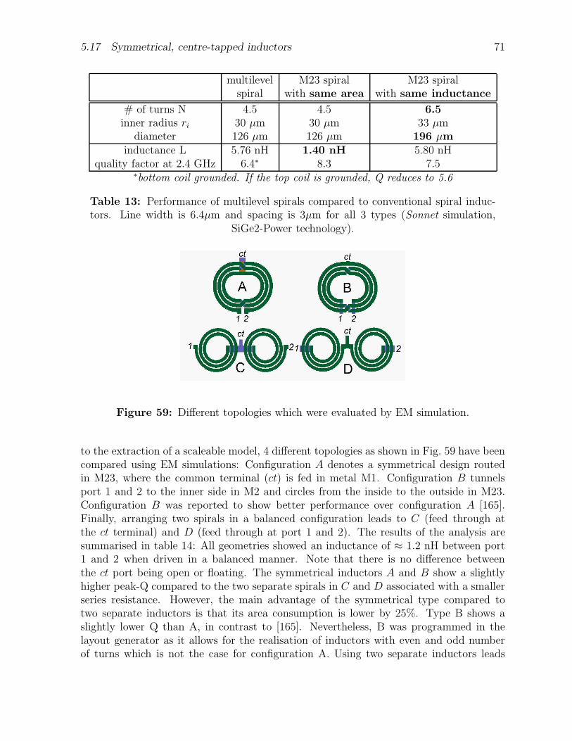
5.17 Symmetrical, centre-tapped inductors 71
multilevel M23 spiral M23 spiralspiral with same area with same inductance
# of turns N 4.5 4.5 6.5inner radius ri 30 µm 30 µm 33 µm
diameter 126 µm 126 µm 196 µminductance L 5.76 nH 1.40 nH 5.80 nH
quality factor at 2.4 GHz 6.4∗ 8.3 7.5∗bottom coil grounded. If the top coil is grounded, Q reduces to 5.6
Table 13: Performance of multilevel spirals compared to conventional spiral induc-tors. Line width is 6.4µm and spacing is 3µm for all 3 types (Sonnet simulation,
SiGe2-Power technology).
Figure 59: Different topologies which were evaluated by EM simulation.
to the extraction of a scaleable model, 4 different topologies as shown in Fig. 59 have beencompared using EM simulations: Configuration A denotes a symmetrical design routedin M23, where the common terminal (ct) is fed in metal M1. Configuration B tunnelsport 1 and 2 to the inner side in M2 and circles from the inside to the outside in M23.Configuration B was reported to show better performance over configuration A [165].Finally, arranging two spirals in a balanced configuration leads to C (feed through atthe ct terminal) and D (feed through at port 1 and 2). The results of the analysis aresummarised in table 14: All geometries showed an inductance of ≈ 1.2 nH between port1 and 2 when driven in a balanced manner. Note that there is no difference betweenthe ct port being open or floating. The symmetrical inductors A and B show a slightlyhigher peak-Q compared to the two separate spirals in C and D associated with a smallerseries resistance. However, the main advantage of the symmetrical type compared totwo separate inductors is that its area consumption is lower by 25%. Type B shows aslightly lower Q than A, in contrast to [165]. Nevertheless, B was programmed in thelayout generator as it allows for the realisation of inductors with even and odd numberof turns which is not the case for configuration A. Using two separate inductors leads
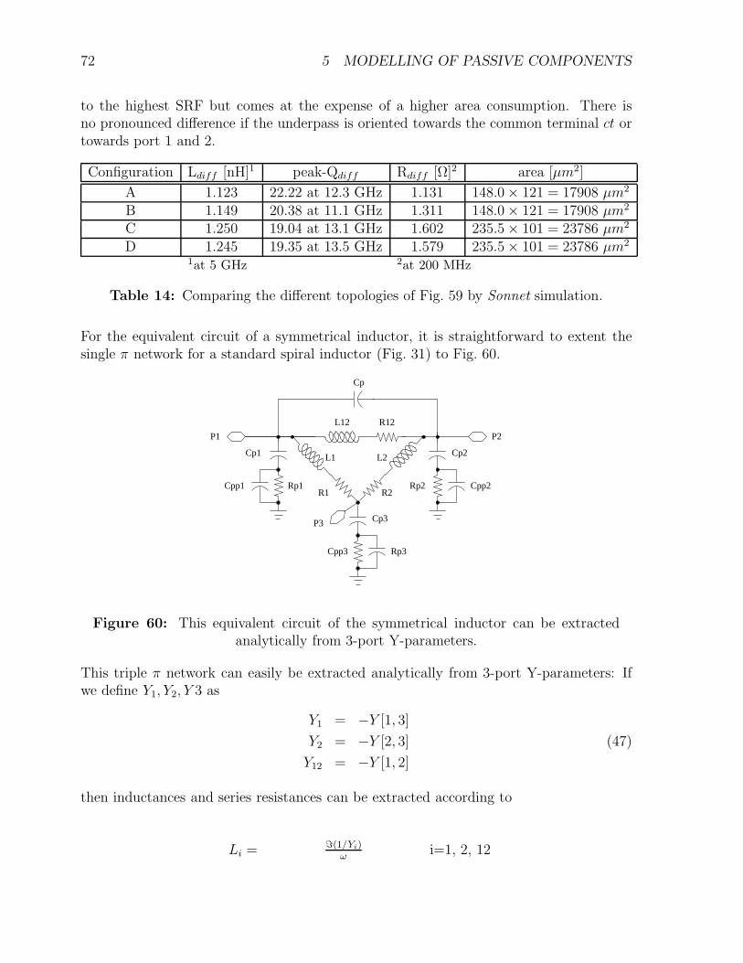
72 5 MODELLING OF PASSIVE COMPONENTS
to the highest SRF but comes at the expense of a higher area consumption. There isno pronounced difference if the underpass is oriented towards the common terminal ct ortowards port 1 and 2.
Configuration Ldiff [nH]1 peak-Qdiff Rdiff [Ω]2 area [µm2]
A 1.123 22.22 at 12.3 GHz 1.131 148.0 × 121 = 17908 µm2
B 1.149 20.38 at 11.1 GHz 1.311 148.0 × 121 = 17908 µm2
C 1.250 19.04 at 13.1 GHz 1.602 235.5 × 101 = 23786 µm2
D 1.245 19.35 at 13.5 GHz 1.579 235.5 × 101 = 23786 µm2
1at 5 GHz 2at 200 MHz
Table 14: Comparing the different topologies of Fig. 59 by Sonnet simulation.
For the equivalent circuit of a symmetrical inductor, it is straightforward to extent thesingle π network for a standard spiral inductor (Fig. 31) to Fig. 60.
Rp1
Cp1
Cpp1 Rp2 Cpp2
P2P1
L1
L12 R12
R1 R2
L2
P3
Cp2
Cp3
Rp3Cpp3
Cp
Figure 60: This equivalent circuit of the symmetrical inductor can be extractedanalytically from 3-port Y-parameters.
This triple π network can easily be extracted analytically from 3-port Y-parameters: Ifwe define Y1, Y2, Y 3 as
Y1 = −Y [1, 3]
Y2 = −Y [2, 3] (47)
Y12 = −Y [1, 2]
then inductances and series resistances can be extracted according to
Li = =(1/Yi)ω
i=1, 2, 12
5.17 Symmetrical, centre-tapped inductors 73
Ri = <(1/Yi) i=1, 2, 12 (48)
YPi = Y [i, 1] + Y [i, 2] + Y [i, 3] i=1, 2, 3 (49)
where YP1, YP2, YP3 are used to derive oxide capacitances and substrate networks. Dueto the positive coupling between the turns, Ldiff from table 14 (the balanced inductancebetween port 1 and 2) is larger than L1 + L2. Therefore, L12 in Fig. 60 is a negativeinductance, the same is true for resistor R12. While this is no problem for a SPICE-basedcircuit simulator, some engineers prefer to substitute the negative inductance L12 by acoupling factor κ. That way, the three inductors L1, L2 and L12 are transformed into twoinductors L∗
1, L∗2 and one coupling factor κ.
L∗1 =
L1 · (L2 + L12)
L1 + L2 + L12
L∗2 =
L2 · (L1 + L12)
L1 + L2 + L12
(50)
κ = −√
L1 · L2
(L1 + L12) · (L2 + L12)
with κ defined as
κ = − L∗12√
L∗1 · L∗
2
(51)
As an example, extracting the symmetrical inductor in Fig. 61 according to the equi-valent circuit in Fig. 60, results in L1 = L2 = 0, 2545 nH and L12 = −0, 876 nH . Thebalanced inductance (port 3 open) is then [1/L12 + 1/(L1 + L2)]
−1 = 1.215nH . This canbe transformed into two coupled inductors of L∗
1 = L∗2 = 0, 431 nH and κ = 0, 41. The
balanced inductance (port 3 open) is then 2(1 + κ)L∗1 = 1.215 nH , showing that both
representations are electrically identical.
EM simulation of symmetrical inductors is straightforward, as just a 3rd port is added(see Fig. 62).
How to measure 3-port S-parameters with a 2-port test set, as well as a comparisonbetween measurements and EM simulation is shown in appendix C.6: Fig. 145 compareson-wafer measurements to EM simulations for three different symmetrical inductors andgets reasonable agreement. Due to that, for simplicity, the models have been extractedfrom Sonnet EM simulations.
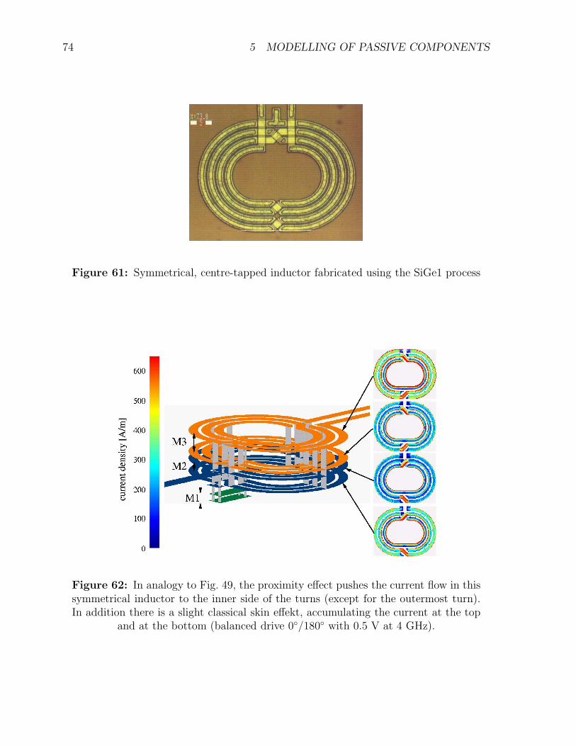
74 5 MODELLING OF PASSIVE COMPONENTS
Figure 61: Symmetrical, centre-tapped inductor fabricated using the SiGe1 process
Figure 62: In analogy to Fig. 49, the proximity effect pushes the current flow in thissymmetrical inductor to the inner side of the turns (except for the outermost turn).In addition there is a slight classical skin effekt, accumulating the current at the top
and at the bottom (balanced drive 0/180 with 0.5 V at 4 GHz).
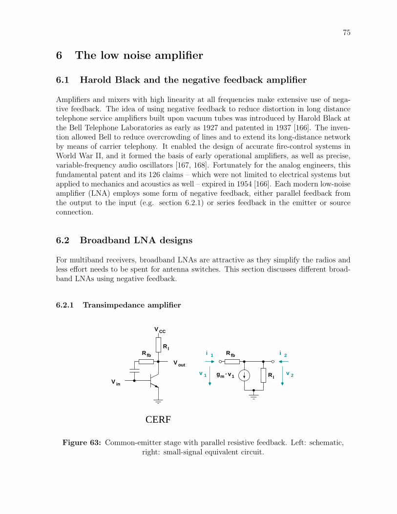
75
6 The low noise amplifier
6.1 Harold Black and the negative feedback amplifier
Amplifiers and mixers with high linearity at all frequencies make extensive use of nega-tive feedback. The idea of using negative feedback to reduce distortion in long distancetelephone service amplifiers built upon vacuum tubes was introduced by Harold Black atthe Bell Telephone Laboratories as early as 1927 and patented in 1937 [166]. The inven-tion allowed Bell to reduce overcrowding of lines and to extend its long-distance networkby means of carrier telephony. It enabled the design of accurate fire-control systems inWorld War II, and it formed the basis of early operational amplifiers, as well as precise,variable-frequency audio oscillators [167, 168]. Fortunately for the analog engineers, thisfundamental patent and its 126 claims – which were not limited to electrical systems butapplied to mechanics and acoustics as well – expired in 1954 [166]. Each modern low-noiseamplifier (LNA) employs some form of negative feedback, either parallel feedback fromthe output to the input (e.g. section 6.2.1) or series feedback in the emitter or sourceconnection.
6.2 Broadband LNA designs
For multiband receivers, broadband LNAs are attractive as they simplify the radios andless effort needs to be spent for antenna switches. This section discusses different broad-band LNAs using negative feedback.
6.2.1 Transimpedance amplifier
V in
V out
V CC
R lR fb
R l
2i
2
1i
1v
R fb
1v vmg
CERF
Figure 63: Common-emitter stage with parallel resistive feedback. Left: schematic,right: small-signal equivalent circuit.
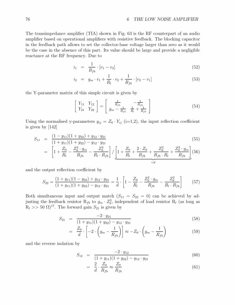
76 6 THE LOW NOISE AMPLIFIER
The transimpedance amplifier (TIA) shown in Fig. 63 is the RF counterpart of an audioamplifier based on operational amplifiers with resistive feedback. The blocking capacitorin the feedback path allows to set the collector-base voltage larger than zero as it wouldbe the case in the absence of this part. Its value should be large and provide a negligiblereactance at the RF frequency. Due to
i1 =1
Rfb· [v1 − v2] (52)
i2 = gm · v1 +1
Rl· v2 +
1
Rfb· [v2 − v1] (53)
the Y-parameter matrix of this simple circuit is given by
[
Y11 Y12
Y21 Y22
]
=
1Rfb
− 1Rfb
gm − 1Rfb
1Rl
+ 1Rfb
(54)
Using the normalised y-parameters yij = Z0 · Yij (i=1,2), the input reflection coefficientis given by [142]
S11 =(1 − y11)(1 + y22) + y12 · y21
(1 + y11)(1 + y22) − y12 · y21
(55)
=
[
1 +Z0
Rl
− Z20 · gm
Rfb
− Z20
Rl · Rfb
]
/
[
1 +Z0
Rl
+2 · Z0
Rfb
+Z2
0
Rfb · Rl
+Z2
0 · gm
Rfb
]
︸ ︷︷ ︸
=d
(56)
and the output reflection coefficient by
S22 =(1 + y11)(1 − y22) + y12 · y21
(1 + y11)(1 + y22) − y12 · y21=
1
d·[
1 − Z0
Rl− Z2
0 · gm
Rfb− Z2
0
Rl · Rfb
]
(57)
Both simultaneous input and output match (S11 = S22 = 0) can be achieved by ad-justing the feedback resistor Rfb to gm · Z2
0 , independent of load resistor Rl (as long asRl >> 50 Ω)17. The forward gain S21 is given by
S21 =−2 · y21
(1 + y11)(1 + y22) − y12 · y21(58)
=Z0
d·[
−2 ·(
gm − 1
Rfb
)]
≈ −Z0 ·(
gm − 1
Rfb
)
(59)
and the reverse isolation by
S12 =−2 · y12
(1 + y11)(1 + y22) − y12 · y21(60)
=2
d· Z0
Rfb≈ Z0
Rfb(61)
6.2 Broadband LNA designs 77
IC gm Rl Rfb S21 S12 S11 S22 k ∆
3mA 0.118 S 300 Ω 300 Ω 13.20 dB -17.54 dB 0.062〈0 0.071〈180 1.12 0.605mA 0.197 S 500 Ω 500 Ω 18.58 dB -21.19 dB 0.046〈0 0.041〈180 1.04 0.74
Table 15: S-parameter set of a CERF LNA using an ideal transistor and Eqns. 54-61.Rfb = gm ·Z2
0 results in simultaneous input and output match. Rl has been chosen tobe equal to Rfb.
Table 15 shows the exact results of an ideal TIA for 3 and 5 mA of bias current: As can beseen, even when using an ideal transistor, due to the strong feedback the reverse isolationis only slightly higher than the gain, leading to a very low Rollett stability factor whichis given for a linear twoport by [169, 170]
k =1 + |∆|2 − |S11|2 − |S22|2
2 · |S21 · S12|with ∆ = S11 · S22 − S12 · S21 (62)
The necessary and sufficient conditions of unconditionally stability for any combinationof source and load impedance are k > 1 and |∆| < 1 [65]. If one of these conditionsis not met (e.g. k < 1), the circuit is only conditionally stable (= potentially unstable)and oscillation may occur with a certain combination of source and/or load impedancepresented to the transistor [65, 171]. Therefore it is essential that the k-factor is aboveunity for all frequencies where the device has substantial gain. Low stability is not just aproblem of bipolar LNAs with parallel feedback but it also occurs for other technologies,e.g. MESFET [172, 173].While S-parameters are useful for small-signal gain, noise and stability analysis, more real-ity is captured by using an ideal BJT large signal model consisting solely of an exponentialcurrent-versus-voltage characteristics
IC = I0 · eVBEkBT with I0 ≈ 10−16A, (63)
infinite current gain, no dependency of collector current IC on collector voltage (infiniteEarly voltage) and zero parasitic resistors and capacitances (”Level-0” model) [174]: Aload resistor of 500 Ω drops 2.5 V at a current of 5 mA leads, making this circuit unsuitedfor 2.7 – 3.3 V circuit design. The 3 mA version – due to the low feedback resistor Rfb –shows already a NF of 1.41 dB even with this ideal transistor containing just collector shotnoise and no ohmic resistances and no base current (see table 16). Both minimum noisefigure NFmin and equivalent noise resistance Rn in table 16 increase further by addinga real transistor’s base and emitter resistance and finite current gain. The influence onNFmin can be derived from Hawkins’s comprehensive model for the minimum noise figureof bipolar transistors with varying collector current and frequency [175]. It shows that
17For reasons of voltage drop, Rl is usually chosen to be in the order of Rfb.
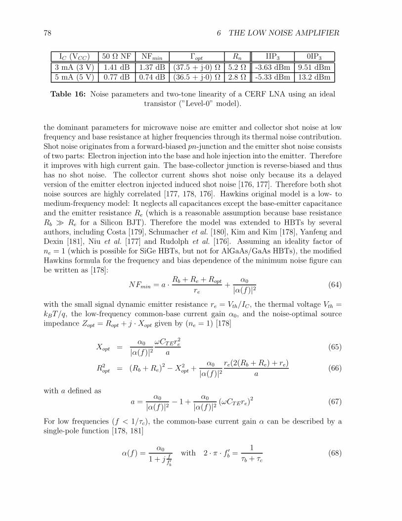
78 6 THE LOW NOISE AMPLIFIER
IC (VCC) 50 Ω NF NFmin Γopt Rn IIP3 0IP3
3 mA (3 V) 1.41 dB 1.37 dB (37.5 + j·0) Ω 5.2 Ω -3.63 dBm 9.51 dBm5 mA (5 V) 0.77 dB 0.74 dB (36.5 + j·0) Ω 2.8 Ω -5.33 dBm 13.2 dBm
Table 16: Noise parameters and two-tone linearity of a CERF LNA using an idealtransistor (”Level-0” model).
the dominant parameters for microwave noise are emitter and collector shot noise at lowfrequency and base resistance at higher frequencies through its thermal noise contribution.Shot noise originates from a forward-biased pn-junction and the emitter shot noise consistsof two parts: Electron injection into the base and hole injection into the emitter. Thereforeit improves with high current gain. The base-collector junction is reverse-biased and thushas no shot noise. The collector current shows shot noise only because its a delayedversion of the emitter electron injected induced shot noise [176, 177]. Therefore both shotnoise sources are highly correlated [177, 178, 176]. Hawkins original model is a low- tomedium-frequency model: It neglects all capacitances except the base-emitter capacitanceand the emitter resistance Re (which is a reasonable assumption because base resistanceRb Re for a Silicon BJT). Therefore the model was extended to HBTs by severalauthors, including Costa [179], Schumacher et al. [180], Kim and Kim [178], Yanfeng andDexin [181], Niu et al. [177] and Rudolph et al. [176]. Assuming an ideality factor ofne = 1 (which is possible for SiGe HBTs, but not for AlGaAs/GaAs HBTs), the modifiedHawkins formula for the frequency and bias dependence of the minimum noise figure canbe written as [178]:
NFmin = a · Rb + Re + Ropt
re+
α0
|α(f)|2 (64)
with the small signal dynamic emitter resistance re = Vth/IC , the thermal voltage Vth =kBT/q, the low-frequency common-base current gain α0, and the noise-optimal sourceimpedance Zopt = Ropt + j · Xopt given by (ne = 1) [178]
Xopt =α0
|α(f)|2ωCTEr2
e
a(65)
R2opt = (Rb + Re)
2 − X2opt +
α0
|α(f)|2re(2(Rb + Re) + re)
a(66)
with a defined as
a =α0
|α(f)|2 − 1 +α0
|α(f)|2 (ωCTEre)2 (67)
For low frequencies (f < 1/τc), the common-base current gain α can be described by asingle-pole function [178, 181]
α(f) =α0
1 + j ff ′
b
with 2 · π · f ′b =
1
τb + τc(68)
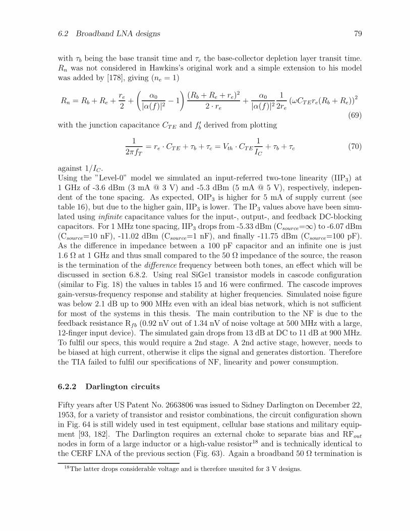
6.2 Broadband LNA designs 79
with τb being the base transit time and τc the base-collector depletion layer transit time.Rn was not considered in Hawkins’s original work and a simple extension to his modelwas added by [178], giving (ne = 1)
Rn = Rb + Re +re
2+
(
α0
|α(f)|2 − 1
)
(Rb + Re + re)2
2 · re+
α0
|α(f)|21
2re(ωCTEre(Rb + Re))
2
(69)with the junction capacitance CTE and f ′
b derived from plotting
1
2πfT= re · CTE + τb + τc = Vth · CTE
1
IC+ τb + τc (70)
against 1/IC.Using the ”Level-0” model we simulated an input-referred two-tone linearity (IIP3) at1 GHz of -3.6 dBm (3 mA @ 3 V) and -5.3 dBm (5 mA @ 5 V), respectively, indepen-dent of the tone spacing. As expected, OIP3 is higher for 5 mA of supply current (seetable 16), but due to the higher gain, IIP3 is lower. The IP3 values above have been simu-lated using infinite capacitance values for the input-, output-, and feedback DC-blockingcapacitors. For 1 MHz tone spacing, IIP3 drops from -5.33 dBm (Csource=∞) to -6.07 dBm(Csource=10 nF), -11.02 dBm (Csource=1 nF), and finally -11.75 dBm (Csource=100 pF).As the difference in impedance between a 100 pF capacitor and an infinite one is just1.6 Ω at 1 GHz and thus small compared to the 50 Ω impedance of the source, the reasonis the termination of the difference frequency between both tones, an effect which will bediscussed in section 6.8.2. Using real SiGe1 transistor models in cascode configuration(similar to Fig. 18) the values in tables 15 and 16 were confirmed. The cascode improvesgain-versus-frequency response and stability at higher frequencies. Simulated noise figurewas below 2.1 dB up to 900 MHz even with an ideal bias network, which is not sufficientfor most of the systems in this thesis. The main contribution to the NF is due to thefeedback resistance Rfb (0.92 nV out of 1.34 nV of noise voltage at 500 MHz with a large,12-finger input device). The simulated gain drops from 13 dB at DC to 11 dB at 900 MHz.To fulfil our specs, this would require a 2nd stage. A 2nd active stage, however, needs tobe biased at high current, otherwise it clips the signal and generates distortion. Thereforethe TIA failed to fulfil our specifications of NF, linearity and power consumption.
6.2.2 Darlington circuits
Fifty years after US Patent No. 2663806 was issued to Sidney Darlington on December 22,1953, for a variety of transistor and resistor combinations, the circuit configuration shownin Fig. 64 is still widely used in test equipment, cellular base stations and military equip-ment [93, 182]. The Darlington requires an external choke to separate bias and RFout
nodes in form of a large inductor or a high-value resistor18 and is technically identical tothe CERF LNA of the previous section (Fig. 63). Again a broadband 50 Ω termination is
18The latter drops considerable voltage and is therefore unsuited for 3 V designs.
80 6 THE LOW NOISE AMPLIFIER
V CC
V in
V out
V CC
V out
V in
V CC
V in
V out
V in
R1
R2
R3 R4
V out
and bias
1N
CEXCE
1N
CBXIN
1 N
CEXCBDarlington
Figure 64: Various broad-band LNA topologies
achieved by setting the feedback resistor R1 = gm ·Z20 and due to R1 the noise figure of the
circuit is typically 0.65 dB above the noise figure of the transistor itself [93]. R3 is con-siderably larger than the series feedback resistor R4 and – together with R2 – mainly setsthe bias current. The second BJT delivers the main contribution to the total transcon-ductance. Fabricated in advanced SiGe HBT [93] or InGaP HBT technologies [182, 183],they achieve noise figures of 2.3 - 5.0 dB, gains of 16-21 dB and OIP3’s of 20-36 dBm inthe 0-2 GHz range at currents ranging from 20 to 150 mA at 4 to 8 V supply voltage.For a detailed investigation of the Darlington amplifier see [93]. While Darlingtons areexcellent driver amplifiers to PAs in broadband transmit systems, they did not fulfil thelow-noise and low-power requirements of the LNAs to be developed in this thesis.
6.2 Broadband LNA designs 81
6.2.3 Transformer based LNAs
LNAs with excellent linearity above 5 GHz have recently been reported using on-chip,trifilar transformers [184, 185]. A study on integrated transformers in Atmel’s SiGe tech-nologies [186] revealed that the losses are too high for LNA applications below 5 GHz,even when using a small transformer tuned to the operating frequency by MIM capacitors.Therefore this section focuses on amplifiers using discrete transformers, where widebandLNAs with excellent linearity have been reported at HF/VHF frequencies for ham radioapplications using trifilar transformers (e.g. the Norton amplifier [187, 188, 189]19).The wide band LNA using transformer feedback from collector to base (CEXCB inFig. 64), was simulated with an IIP3 of 16 dBm at 500 MHz and 50 kHz 2-tone spacing,a gain of 15.5 dB and sub-1 dB noise figure, consuming 6 mA from a 3 V supply. Thetransformation ratio of the ideal transformer was 1:N = 1:4. Using a 1:5 transformer, anIIP3 of 10.5dBm is possible with 16.7dB of gain. This circuit features excellent NF andS22 properties and would have been an ideal solution for the TETRA/TETRAPOL LNA,but stability is critical and the input impedance is far from 50 Ω at low frequencies.Using the same configuration with transformer feedback from the collector to the emitter,(CEXCE in Fig. 64), resulted in an IIP3 of 11.3 dBm with 14.9 dB of gain at 500 MHz+/- 25 kHz while the circuit consumes 6.5 mA at 3 V. A 1:5 transformer reduces IIP3
to 9.8 dBm but increases gain to 16.2 dB. Stability is critical, however better than usingcollector-to-base transformer feedback (CEXCB). Again the input impedance is far from50 Ω at low frequencies.In order to achieve a better input return loss across a large frequency band, we finallyinvestigated a common-base input stage, where a broadband Zin is given by re + Re =Vth/IC + Re with Re being the emitter resistance and the diffusion capacitance being ne-glected at low frequencies. While a collector current of IC = 0.5 mA leads to 50 Ω inputimpedance, a reasonable IIP3 requires currents of several mA. In order to match the 50 Ωsource to this low impedance, a transformer was used (CBXIN in Fig. 64). Biasing the RFstage with 4 mA, a 2:1 transformer yields an almost perfect match due to the impedancetransformation of 4:1. In addition the transformer provided a current gain of 4 (6dB). NFwas minimised by using three 6 finger devices but the high parasitic collector base capaci-tance led to an inherent gain roll off due to the formation of a low-pass at the output node,unless cascaded by an additional, smaller common-base HBT. As the common-base devicehas unity current gain, power gain can only be obtained by impedance transformation.This requires a large value for the load resistor, followed by an emitter follower (EF) totransfer the high voltage swing at the load resistor to 50 Ω at port 2. While the EF canprovide infinite output current when the voltage goes low at its emitter node, 180 laterthe EF itself switches off and the current source of the follower has to sink the completecurrent from port 2. In order to prevent clipping of the waveform, a large current in theEF’s current source is needed and linearity is therefore directly related to the current inthe EF. An IIP3 of +6 dBm required a current of 13 mA in the EF. In total, this circuit
19 A resimulation showed that the Norton amplifier suffers from stability problems due to the lowreverse isolation.
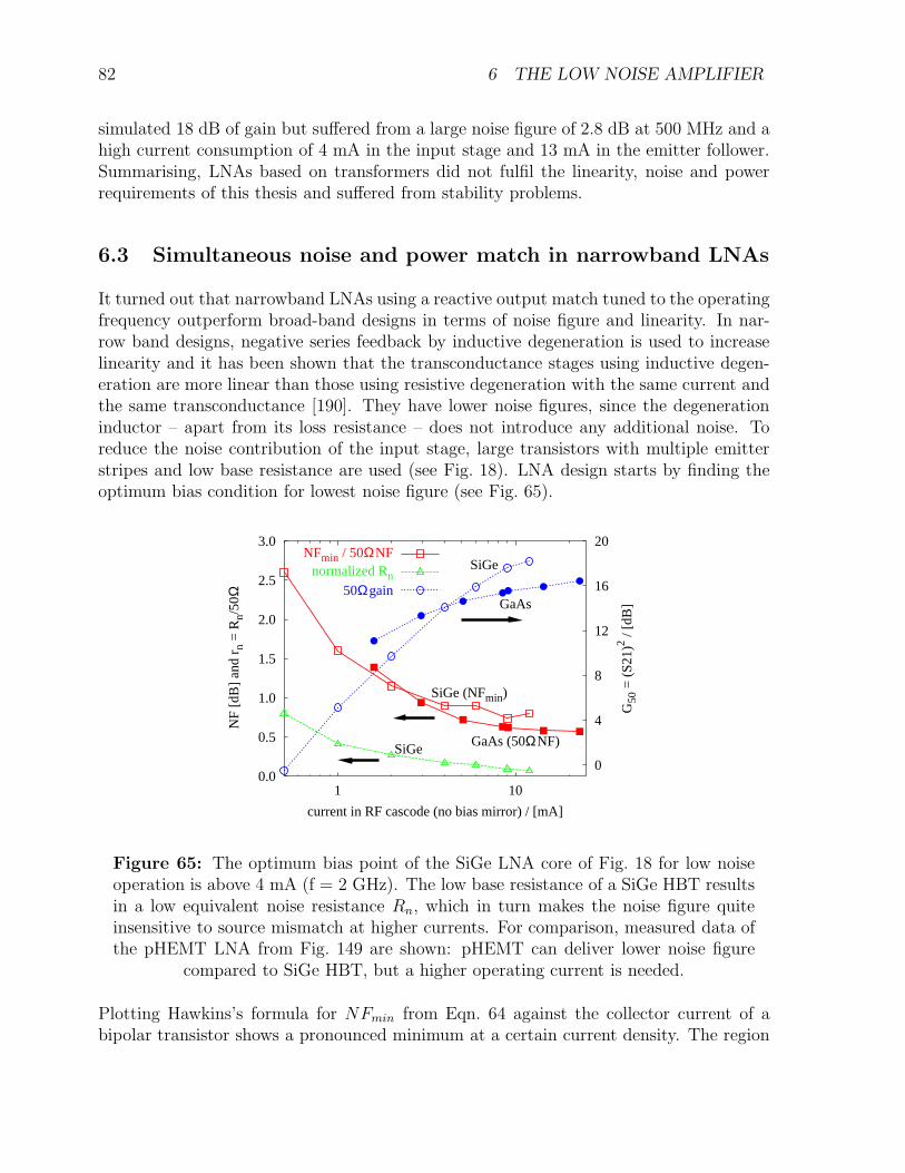
82 6 THE LOW NOISE AMPLIFIER
simulated 18 dB of gain but suffered from a large noise figure of 2.8 dB at 500 MHz and ahigh current consumption of 4 mA in the input stage and 13 mA in the emitter follower.Summarising, LNAs based on transformers did not fulfil the linearity, noise and powerrequirements of this thesis and suffered from stability problems.
6.3 Simultaneous noise and power match in narrowband LNAs
It turned out that narrowband LNAs using a reactive output match tuned to the operatingfrequency outperform broad-band designs in terms of noise figure and linearity. In nar-row band designs, negative series feedback by inductive degeneration is used to increaselinearity and it has been shown that the transconductance stages using inductive degen-eration are more linear than those using resistive degeneration with the same current andthe same transconductance [190]. They have lower noise figures, since the degenerationinductor – apart from its loss resistance – does not introduce any additional noise. Toreduce the noise contribution of the input stage, large transistors with multiple emitterstripes and low base resistance are used (see Fig. 18). LNA design starts by finding theoptimum bias condition for lowest noise figure (see Fig. 65).
0.0
0.5
1.0
1.5
2.0
2.5
3.0
1 10
0
4
8
12
16
20
NF
[dB
] an
d r n
= R
n/50
Ω
G50
= (
S21)
2 / [d
B]
current in RF cascode (no bias mirror) / [mA]
SiGe (NFmin)
GaAs (50Ω NF)
SiGe
GaAs
SiGe
NFmin / 50Ω NFnormalized Rn
50Ω gain
Figure 65: The optimum bias point of the SiGe LNA core of Fig. 18 for low noiseoperation is above 4 mA (f = 2 GHz). The low base resistance of a SiGe HBT resultsin a low equivalent noise resistance Rn, which in turn makes the noise figure quiteinsensitive to source mismatch at higher currents. For comparison, measured data ofthe pHEMT LNA from Fig. 149 are shown: pHEMT can deliver lower noise figure
compared to SiGe HBT, but a higher operating current is needed.
Plotting Hawkins’s formula for NFmin from Eqn. 64 against the collector current of abipolar transistor shows a pronounced minimum at a certain current density. The region
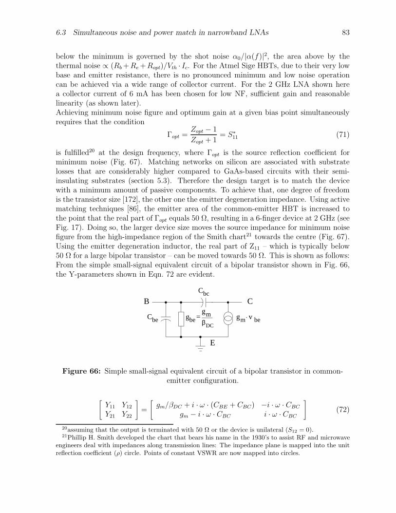
6.3 Simultaneous noise and power match in narrowband LNAs 83
below the minimum is governed by the shot noise α0/|α(f)|2, the area above by thethermal noise ∝ (Rb +Re +Ropt)/Vth · Ic. For the Atmel Sige HBTs, due to their very lowbase and emitter resistance, there is no pronounced minimum and low noise operationcan be achieved via a wide range of collector current. For the 2 GHz LNA shown herea collector current of 6 mA has been chosen for low NF, sufficient gain and reasonablelinearity (as shown later).Achieving minimum noise figure and optimum gain at a given bias point simultaneouslyrequires that the condition
Γopt =Zopt − 1
Zopt + 1= S∗
11 (71)
is fulfilled20 at the design frequency, where Γopt is the source reflection coefficient forminimum noise (Fig. 67). Matching networks on silicon are associated with substratelosses that are considerably higher compared to GaAs-based circuits with their semi-insulating substrates (section 5.3). Therefore the design target is to match the devicewith a minimum amount of passive components. To achieve that, one degree of freedomis the transistor size [172], the other one the emitter degeneration impedance. Using activematching techniques [86], the emitter area of the common-emitter HBT is increased tothe point that the real part of Γopt equals 50 Ω, resulting in a 6-finger device at 2 GHz (seeFig. 17). Doing so, the larger device size moves the source impedance for minimum noisefigure from the high-impedance region of the Smith chart21 towards the centre (Fig. 67).Using the emitter degeneration inductor, the real part of Z11 – which is typically below50 Ω for a large bipolar transistor – can be moved towards 50 Ω. This is shown as follows:From the simple small-signal equivalent circuit of a bipolar transistor shown in Fig. 66,the Y-parameters shown in Eqn. 72 are evident.
mg v beC
C
C
.
B
beg =gm
DCβ
E
be
bc
Figure 66: Simple small-signal equivalent circuit of a bipolar transistor in common-emitter configuration.
[
Y11 Y12
Y21 Y22
]
=
[
gm/βDC + i · ω · (CBE + CBC) −i · ω · CBC
gm − i · ω · CBC i · ω · CBC
]
(72)
20assuming that the output is terminated with 50 Ω or the device is unilateral (S12 = 0).21Phillip H. Smith developed the chart that bears his name in the 1930’s to assist RF and microwave
engineers deal with impedances along transmission lines: The impedance plane is mapped into the unitreflection coefficient (ρ) circle. Points of constant VSWR are now mapped into circles.
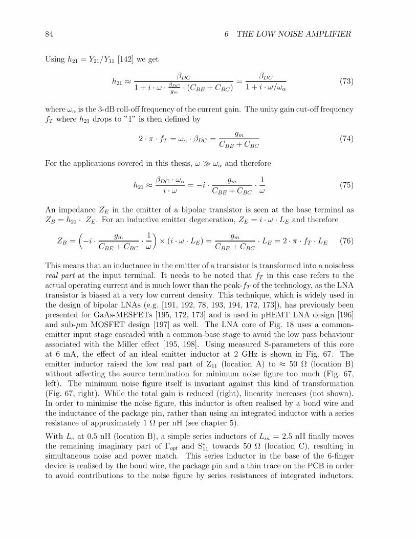
84 6 THE LOW NOISE AMPLIFIER
Using h21 = Y21/Y11 [142] we get
h21 ≈βDC
1 + i · ω · βDC
gm· (CBE + CBC)
=βDC
1 + i · ω/ωα(73)
where ωα is the 3-dB roll-off frequency of the current gain. The unity gain cut-off frequencyfT where h21 drops to ”1” is then defined by
2 · π · fT = ωα · βDC =gm
CBE + CBC(74)
For the applications covered in this thesis, ω ωα and therefore
h21 ≈βDC · ωα
i · ω = −i · gm
CBE + CBC· 1
ω(75)
An impedance ZE in the emitter of a bipolar transistor is seen at the base terminal asZB = h21 · ZE. For an inductive emitter degeneration, ZE = i · ω · LE and therefore
ZB =(
−i · gm
CBE + CBC
· 1
ω
)
× (i · ω · LE) =gm
CBE + CBC
· LE = 2 · π · fT · LE (76)
This means that an inductance in the emitter of a transistor is transformed into a noiselessreal part at the input terminal. It needs to be noted that fT in this case refers to theactual operating current and is much lower than the peak-fT of the technology, as the LNAtransistor is biased at a very low current density. This technique, which is widely used inthe design of bipolar LNAs (e.g. [191, 192, 78, 193, 194, 172, 173]), has previously beenpresented for GaAs-MESFETs [195, 172, 173] and is used in pHEMT LNA design [196]and sub-µm MOSFET design [197] as well. The LNA core of Fig. 18 uses a common-emitter input stage cascaded with a common-base stage to avoid the low pass behaviourassociated with the Miller effect [195, 198]. Using measured S-parameters of this coreat 6 mA, the effect of an ideal emitter inductor at 2 GHz is shown in Fig. 67. Theemitter inductor raised the low real part of Z11 (location A) to ≈ 50 Ω (location B)without affecting the source termination for minimum noise figure too much (Fig. 67,left). The minimum noise figure itself is invariant against this kind of transformation(Fig. 67, right). While the total gain is reduced (right), linearity increases (not shown).In order to minimise the noise figure, this inductor is often realised by a bond wire andthe inductance of the package pin, rather than using an integrated inductor with a seriesresistance of approximately 1 Ω per nH (see chapter 5).
With Le at 0.5 nH (location B), a simple series inductors of Lin = 2.5 nH finally movesthe remaining imaginary part of Γopt and S∗
11 towards 50 Ω (location C), resulting insimultaneous noise and power match. This series inductor in the base of the 6-fingerdevice is realised by the bond wire, the package pin and a thin trace on the PCB in orderto avoid contributions to the noise figure by series resistances of integrated inductors.
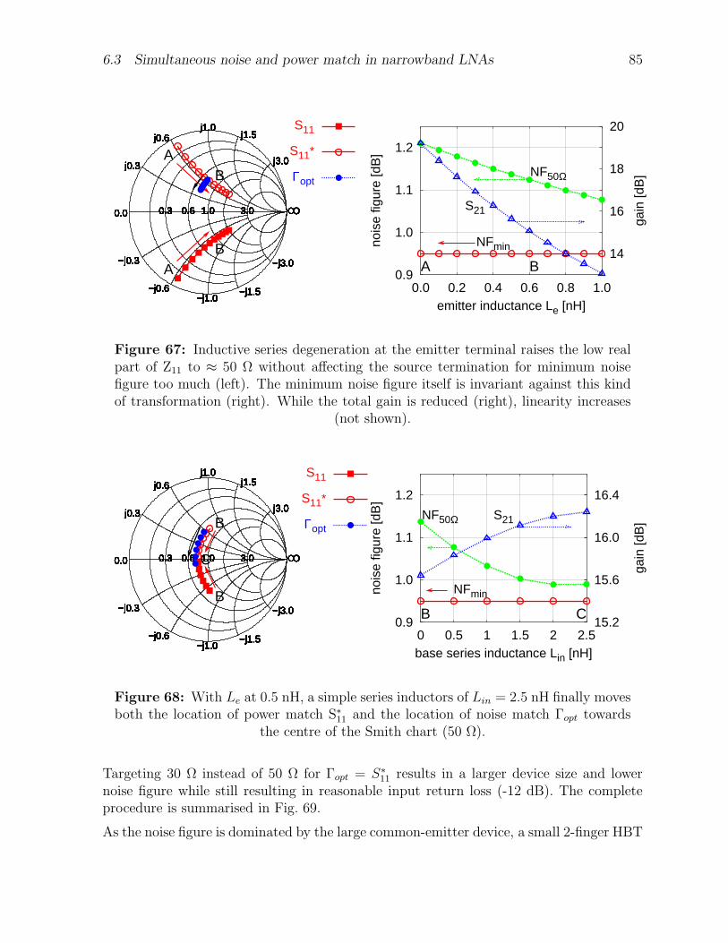
6.3 Simultaneous noise and power match in narrowband LNAs 85
j0.3
j0.6j1.0
j1.5
j3.0
−j0.3
−j0.6−j1.0
−j1.5
−j3.0
0.3 0.6 1.0 3.00.0 8
j0.3
j0.6j1.0
j1.5
j3.0
−j0.3
−j0.6−j1.0
−j1.5
−j3.0
0.3 0.6 1.0 3.00.0 8
j0.3
j0.6j1.0
j1.5
j3.0
−j0.3
−j0.6−j1.0
−j1.5
−j3.0
0.3 0.6 1.0 3.00.0 8
j0.3
j0.6j1.0
j1.5
j3.0
−j0.3
−j0.6−j1.0
−j1.5
−j3.0
0.3 0.6 1.0 3.00.0 8
j0.3
j0.6j1.0
j1.5
j3.0
−j0.3
−j0.6−j1.0
−j1.5
−j3.0
0.3 0.6 1.0 3.00.0 8
j0.3
j0.6j1.0
j1.5
j3.0
−j0.3
−j0.6−j1.0
−j1.5
−j3.0
0.3 0.6 1.0 3.00.0 8
j0.3
j0.6j1.0
j1.5
j3.0
−j0.3
−j0.6−j1.0
−j1.5
−j3.0
0.3 0.6 1.0 3.00.0 8
j0.3
j0.6j1.0
j1.5
j3.0
−j0.3
−j0.6−j1.0
−j1.5
−j3.0
0.3 0.6 1.0 3.00.0 8
j0.3
j0.6j1.0
j1.5
j3.0
−j0.3
−j0.6−j1.0
−j1.5
−j3.0
0.3 0.6 1.0 3.00.0 8
j0.3
j0.6j1.0
j1.5
j3.0
−j0.3
−j0.6−j1.0
−j1.5
−j3.0
0.3 0.6 1.0 3.00.0 8
j0.3
j0.6j1.0
j1.5
j3.0
−j0.3
−j0.6−j1.0
−j1.5
−j3.0
0.3 0.6 1.0 3.00.0 8
j0.3
j0.6j1.0
j1.5
j3.0
−j0.3
−j0.6−j1.0
−j1.5
−j3.0
0.3 0.6 1.0 3.00.0 8
j0.3
j0.6j1.0
j1.5
j3.0
−j0.3
−j0.6−j1.0
−j1.5
−j3.0
0.3 0.6 1.0 3.00.0 8
j0.3
j0.6j1.0
j1.5
j3.0
−j0.3
−j0.6−j1.0
−j1.5
−j3.0
0.3 0.6 1.0 3.00.0 8
j0.3
j0.6j1.0
j1.5
j3.0
−j0.3
−j0.6−j1.0
−j1.5
−j3.0
0.3 0.6 1.0 3.00.0 8
j0.3
j0.6j1.0
j1.5
j3.0
−j0.3
−j0.6−j1.0
−j1.5
−j3.0
0.3 0.6 1.0 3.00.0 8
j0.3
j0.6j1.0
j1.5
j3.0
−j0.3
−j0.6−j1.0
−j1.5
−j3.0
0.3 0.6 1.0 3.00.0 8
j0.3
j0.6j1.0
j1.5
j3.0
−j0.3
−j0.6−j1.0
−j1.5
−j3.0
0.3 0.6 1.0 3.00.0 8
j0.3
j0.6j1.0
j1.5
j3.0
−j0.3
−j0.6−j1.0
−j1.5
−j3.0
0.3 0.6 1.0 3.00.0 8
A
A
B
B
S11
S11*
Γopt
0.9
1.0
1.1
1.2
0.0 0.2 0.4 0.6 0.8 1.0
14
16
18
20
nois
e fig
ure
[dB
]
gain
[dB
]
emitter inductance Le [nH]
A B
NFmin
NF50Ω
S21
Figure 67: Inductive series degeneration at the emitter terminal raises the low realpart of Z11 to ≈ 50 Ω without affecting the source termination for minimum noisefigure too much (left). The minimum noise figure itself is invariant against this kindof transformation (right). While the total gain is reduced (right), linearity increases
(not shown).
j0.3
j0.6j1.0
j1.5
j3.0
−j0.3
−j0.6−j1.0
−j1.5
−j3.0
0.3 0.6 1.0 3.00.0 8
j0.3
j0.6j1.0
j1.5
j3.0
−j0.3
−j0.6−j1.0
−j1.5
−j3.0
0.3 0.6 1.0 3.00.0 8
j0.3
j0.6j1.0
j1.5
j3.0
−j0.3
−j0.6−j1.0
−j1.5
−j3.0
0.3 0.6 1.0 3.00.0 8
j0.3
j0.6j1.0
j1.5
j3.0
−j0.3
−j0.6−j1.0
−j1.5
−j3.0
0.3 0.6 1.0 3.00.0 8
j0.3
j0.6j1.0
j1.5
j3.0
−j0.3
−j0.6−j1.0
−j1.5
−j3.0
0.3 0.6 1.0 3.00.0 8
j0.3
j0.6j1.0
j1.5
j3.0
−j0.3
−j0.6−j1.0
−j1.5
−j3.0
0.3 0.6 1.0 3.00.0 8
j0.3
j0.6j1.0
j1.5
j3.0
−j0.3
−j0.6−j1.0
−j1.5
−j3.0
0.3 0.6 1.0 3.00.0 8
j0.3
j0.6j1.0
j1.5
j3.0
−j0.3
−j0.6−j1.0
−j1.5
−j3.0
0.3 0.6 1.0 3.00.0 8
j0.3
j0.6j1.0
j1.5
j3.0
−j0.3
−j0.6−j1.0
−j1.5
−j3.0
0.3 0.6 1.0 3.00.0 8
j0.3
j0.6j1.0
j1.5
j3.0
−j0.3
−j0.6−j1.0
−j1.5
−j3.0
0.3 0.6 1.0 3.00.0 8
j0.3
j0.6j1.0
j1.5
j3.0
−j0.3
−j0.6−j1.0
−j1.5
−j3.0
0.3 0.6 1.0 3.00.0 8
j0.3
j0.6j1.0
j1.5
j3.0
−j0.3
−j0.6−j1.0
−j1.5
−j3.0
0.3 0.6 1.0 3.00.0 8
j0.3
j0.6j1.0
j1.5
j3.0
−j0.3
−j0.6−j1.0
−j1.5
−j3.0
0.3 0.6 1.0 3.00.0 8
j0.3
j0.6j1.0
j1.5
j3.0
−j0.3
−j0.6−j1.0
−j1.5
−j3.0
0.3 0.6 1.0 3.00.0 8
j0.3
j0.6j1.0
j1.5
j3.0
−j0.3
−j0.6−j1.0
−j1.5
−j3.0
0.3 0.6 1.0 3.00.0 8
j0.3
j0.6j1.0
j1.5
j3.0
−j0.3
−j0.6−j1.0
−j1.5
−j3.0
0.3 0.6 1.0 3.00.0 8
j0.3
j0.6j1.0
j1.5
j3.0
−j0.3
−j0.6−j1.0
−j1.5
−j3.0
0.3 0.6 1.0 3.00.0 8
j0.3
j0.6j1.0
j1.5
j3.0
−j0.3
−j0.6−j1.0
−j1.5
−j3.0
0.3 0.6 1.0 3.00.0 8
j0.3
j0.6j1.0
j1.5
j3.0
−j0.3
−j0.6−j1.0
−j1.5
−j3.0
0.3 0.6 1.0 3.00.0 8
B
B
C
S11
S11*
Γopt
0.9
1.0
1.1
1.2
0 0.5 1 1.5 2 2.515.2
15.6
16.0
16.4
nois
e fig
ure
[dB
]
gain
[dB
]base series inductance Lin [nH]
B C
NFmin
NF50Ω S21
Figure 68: With Le at 0.5 nH, a simple series inductors of Lin = 2.5 nH finally movesboth the location of power match S∗
11 and the location of noise match Γopt towardsthe centre of the Smith chart (50 Ω).
Targeting 30 Ω instead of 50 Ω for Γopt = S∗11 results in a larger device size and lower
noise figure while still resulting in reasonable input return loss (-12 dB). The completeprocedure is summarised in Fig. 69.
As the noise figure is dominated by the large common-emitter device, a small 2-finger HBT
86 6 THE LOW NOISE AMPLIFIER
P out P out
P in
P out
P inP in
L e L e
L in
A CB
Figure 69: 3-step simultaneous noise and input match using a minimum number ofreactive components.
can be used in the cascaded common-base output stage. The cascode leads to a higherisolation from the amplifier output to the input, reducing |S12|. This unilateralizationincreases the stability factor k and allows to match input and output independently [173],as the common-emitter stage now drives the constant low impedance of the emitter ofthe common-base transistor making the amplifier insensitive to output load variations.Bandwidth is increased by reduction of the Miller capacitance defined as CM = CCB ·(1 + gm · RL), where CM is the effective shunt capacitance seen at the amplifier input,resulting from the parallel collector-base feedback capacitor CCB. As the load resistanceRL to the common-emitter stage is the dynamic emitter resistance of the common-basestage (1/rE), the Miller capacitance is just twice the base collector capacitance and thusmuch lower than it would be in a normal common-emitter amplifier [199]. This comes atthe expense of additional headroom and a separate pin to block the base of the common-base transistor to GND22. The base of this device is blocked by means of a 5 pF MIMcapacitor. In order to achieve power gain, a high output impedance needs to be presentedto the output of the cascode configuration. As discussed in section 6.2.3, the use ofan EF for impedance transformation is prohibitive for highly linear LNAs as it wouldresult in a very low linearity due to waveform clipping by the EF realistic bias currents.Therefore the 50 Ω output impedance is transformed to a high impedance at the cascodeoutput by means of a passive, integrated LC matching network. In order to feed thebias current to the cascode and to have a DC block at the output, a shunt-L / series-Cconfiguration was used, where the inductor is shunted to the supply rather than GND.As a large inductor is needed, for the GPS and Scuba LNAs the inductor was realised inthe top metallisation of Atmel’s SiGe1 technology (see section 5.7) and for the 2.4 GHzWLAN LNA a multilevel spiral (section 5.16) was used. In order to become independentfrom inductances due to bond wires and parasitic traces on the PCB, the supply voltage
22If the GND of the common-emitter stage and the GND of the capacitor blocking the common-basestage are not separated, the LNA – due to positive feedback from the common bondwire inductance –turns into an oscillator.
6.3 Simultaneous noise and power match in narrowband LNAs 87
was blocked on-chip at 2 GHz with an integrated MIM capacitor of 10 pF, in series toa 5 Ω resistor to damp low frequency resonances, which would result from interaction ofon-chip inductance, bondwire and external SMD blocking capacitor on the PCB. The DCblocking capacitor at the input was not integrated due to noise reasons. As an examplefor this design technique, the noise figure of the UMTS SiGe LNA of the Scuba project(see Fig. 6) as a function of the input impedance is shown in Fig. 70. The measurementshave been performed using a NP5 noise tuner system from atn microwave at the Zentrumfur Mikroelektronik Aargau (ZMA) in Switzerland23. The results confirm this LNA designtechnique and show a minimum NF of ≈ 0.9 dB, just slightly higher than the 0.6-0.8 dBof the SiGe HBT itself. The 50 Ω-NF was measured to be 1.15 dB (see Fig. 137 inappendix A, which is dedicated to the task how to measure low noise figures accurately).
0.1
0.1
0.1
0.2
0.2
0.2
0.3
0.3
0.3
0.4
0.4
0.4
0.5
0.5
0.5
0.6
0.6
0.6
0.7
0.7
0.7
0.8
0.8
0.8
0.9
0.9
0.9
1.0
1.0
1.0
1.2
1.2
1.2
1.4
1.4
1.4
1.6
1.6
1.6
1.8
1.8
1.8
2.0
2.0
2.0
3.0
3.0
3.0
4.0
4.0
4.0
5.0
5.0
5.0
10
10
10
20
20
20
50
50
50
0.2
0.2
0.2
0.2
0.4
0.4
0.4
0.4
0.6
0.6
0.6
0.6
0.8
0.8
0.8
0.8
1.0
1.0
1.0
1.0
20-20
30-30
40-40
50
-50
60
-60
70
-70
80
-80
90
-90
100
-100
110
-110
120
-120
130
-130
140
-140
150
-150
160
-160
170
-170
180
±
90-9
0
85-8
5
80-8
0
75-7
5
70-7
0
65-6
5
60-6
0
55-5
5
50-5
0
45
-45
40
-40
35
-35
30
-30
25
-25
20
-20
15
-15
10
-10
0.04
0.04
0.05
0.05
0.06
0.06
0.07
0.07
0.08
0.08
0.09
0.09
0.1
0.1
0.11
0.11
0.12
0.12
0.13
0.13
0.14
0.14
0.15
0.15
0.16
0.16
0.17
0.17
0.18
0.18
0.190.19
0.2
0.2
0.21
0.210.22
0.220.23
0.230.24
0.24
0.25
0.25
0.26
0.26
0.27
0.27
0.28
0.28
0.29
0.29
0.3
0.3
0.31
0.31
0.32
0.32
0.33
0.33
0.34
0.34
0.35
0.35
0.36
0.36
0.37
0.37
0.38
0.38
0.39
0.39
0.4
0.4
0.41
0.41
0.42
0.42
0.43
0.43
0.44
0.44
0.45
0.45
0.46
0.46
0.47
0.47
0.48
0.48
0.49
0.49
0.0
0.0
AN
GL
E O
F T
RA
NS
MIS
SIO
N C
OE
FF
ICIE
NT
IN D
EG
RE
ES
AN
GL
E O
F R
EF
LE
CT
ION
CO
EF
FIC
IEN
T IN
DE
GR
EE
S
—>
WA
VE
LE
NG
TH
S T
OW
AR
D G
EN
ER
AT
OR
—>
<—
WA
VE
LE
NG
TH
S T
OW
AR
D L
OA
D <
—
IND
UC
TIV
E R
EA
CT
AN
CE
CO
MPO
NEN
T (+jX
/Zo), O
R CAPACIT
IVE SUSCEPTANCE (+jB/Yo)
CAPACITIVE REACTANCE COM
PONEN
T (-
jX/Zo)
, OR
IND
UC
TIV
E S
USC
EP
TA
NC
E (
-jB
/Y
o)
RESISTANCE COMPONENT (R/Zo), OR CONDUCTANCE COMPONENT (G/Yo)
RADIALLY SCALED PARAMETERS
TOWARD LOAD —> <— TOWARD GENERATOR1.11.21.41.61.822.5345102040100
SWR 1∞
12345681015203040
dBS1∞
1234571015 ATTEN
. [dB]
1.1 1.2 1.3 1.4 1.6 1.8 2 3 4 5 10 20 S.W
. LO
SS C
OEFF
1 ∞0 1 2 3 4 5 6 7 8 9 10 12 14 20 30
RTN. LO
SS [dB] ∞
0.010.050.10.20.30.40.50.60.70.80.91
RFL. COEFF, P
0
0.1 0.2 0.4 0.6 0.8 1 1.5 2 3 4 5 6 10 15 RFL. LO
SS [d
B]
∞0
1.1 1.2 1.3 1.4 1.5 1.6 1.7 1.8 1.9 2 2.5 3 4 5 10 S.W
. PEA
K (C
ON
ST. P
)
0 ∞0.10.20.30.40.50.60.70.80.91
RFL. COEFF, E or I 0 0.99 0.95 0.9 0.8 0.7 0.6 0.5 0.4 0.3 0.2 0.1 0 TRA
NSM
. CO
EFF, P
1
CENTER
1 1.1 1.2 1.3 1.4 1.5 1.6 1.7 1.8 1.9 2 TRAN
SM. C
OEFF, E
or I
0.0 0.1 0.2 0.3 0.4 0.5 0.6 0.7 0.8 0.9
ORIGIN
Noise figure at different tuner states
UMTS LNA
8.66.5
2.62.1
2.2
4.6
4.2 1.11.2
0.9
2.80.5
2.2
3.3
7.8
Figure 70: Noise figure of the UMTS LNA for different input impedances, measuredat 1.95 GHz with a NP5 source pull system (atn microwave).
23The large spread of the data points originates from the fact that the diode-based atn tuners –due to losses in the diodes – cannot cover the Smith chart evenly and the low sensitivity makes noisemeasurements below 1 dB difficult.
88 6 THE LOW NOISE AMPLIFIER
6.3.1 Application to CMOS LNAs
The design of sub-µm MOSFET LNAs follows exactly the same design criteria as outlinedbefore [197]. Although scaling of sub- µm gate length becomes difficult [200], it has beenshown for a 0.24 µm CMOS technology that devices with minimum gate length offer thebest noise performance and that the minimum noise figure NFmin just depends on Lg andis independent of the gate width W . So W remains as a parameter to control the sizeof Rn (∝ 1/W ) and the location of Γopt: The high Zopt = 1/(Gopt + j · Bopt) needed foroptimum noise performance of MOSFETS can be decreased towards 50 Ω as Gopt ∝ Wand Bopt ∝ W [197]. The differences to HBT LNA design are
1. Due to the higher equivalent noise resistance Rn (see table 8) the selection of thedevice size of the input transistor is much more critical.
2. Due to the lower transconductance gm the size of the cascode device is much morecritical. The cascode MOS transistor can contribute up to 40% to the total MOSLNA noise figure.
3. Due to the lower operating fT , a larger source inductance is needed to move thereal part of the input impedance towards 50 Ω (Eqn. 76). Due to the higher inputcapacitance, a much larger gate inductance is needed to move S∗
11 and Γopt simul-taneously towards 50 Ω (e.g. 36 nH for a 900 MHz CMOS LNA [197]), makingthe input match more narrowband. Furthermore, this large inductance cannot beprovided by a bondwire and a small inductive trace on the board, as it is usuallythe case for SiGe HBTs, but requires the use of a discrete, high-Q (e.g. wirewound)SMD inductor.
6.4 Bias considerations
While much attention is paid to the 2-6 fast RF transistors of a typical RFIC buildingblock, the optimisation of the bias network is often neglected. The bias network needsto ensure a stable RF performance versus changes in supply voltage and temperature. Itneeds to be insensitive against process variations, as there are in a typical silicon process variations of the poly silicon resistors by up to ± 20 % variations in the MIM capacitors of up to ± 10 % current gains of 100-500 for a SiGe HBT and 40-100 for a Si BJT variations in the threshold voltage of MOS devices.
In addition the bias network needs to ensure low leakage currents in power down mode [201].For an excellent overview about the art of biasing see [202]. Due to the high variation in a
6.4 Bias considerations 89
SiGe HBT’s current gain β, such a device should never be biased by forcing a base currentitself without any feedback via the emitter or collector current. From the semi-empiricalcurrent-voltage relationship the strong temperature dependence of the transconductanceis evident:
IC = I0 × eVBEVth (1 +
VCE
VA
) ≈ I0 × eVBEVth with I0 = A × j0 (77)
gm = y21 =δ(I2)
δ(V1)|δV2=0=
δ(IC)
δ(VBE)=
IC
Vth=
q × IC
kB × T(78)
I0 and j0 are saturation current and saturation current density per area, respectively,which are strongly temperature dependent. From Eqn. 78 its evident that constant smallsignal gain versus temperature dictates the bias current to vary Proportional-To-Abso-lute-Temperature (PTAT). As the resulting drop of P1 dB and IP3 at low temperaturesand bias currents is often undesirable, the slope of current versus temperature is typicallysomewhere between zero and PTAT.The simple LNA bias circuit of Fig. 71 is often used, where the base voltage is fixed bya resistive divider and the emitter current is set by the voltage drop across the emitterresistor. If the impedance of the resistive divider is high, there is considerable voltagedrop due to the base current of the transistor. The strong β-variations from lot to lotin SiGe HBTs therefore result in a large spread of the emitter current. If the impedanceof the divider is too low, it increases the NF of the LNA. The strong dependence of theemitter current on the supply voltage is another drawback for this bias scheme. Withrespect to the temperature the bias current increases only slightly due to the decline ofVBE by 1.5–2 mV/K.
Figure 71: Simple LNA bias network.
Therefore biasing via current mirrors is usually employed (Fig. 72). Mirror ratios arecommonly limited between 1:6 and 1:12, as the finite current gain of the transistors
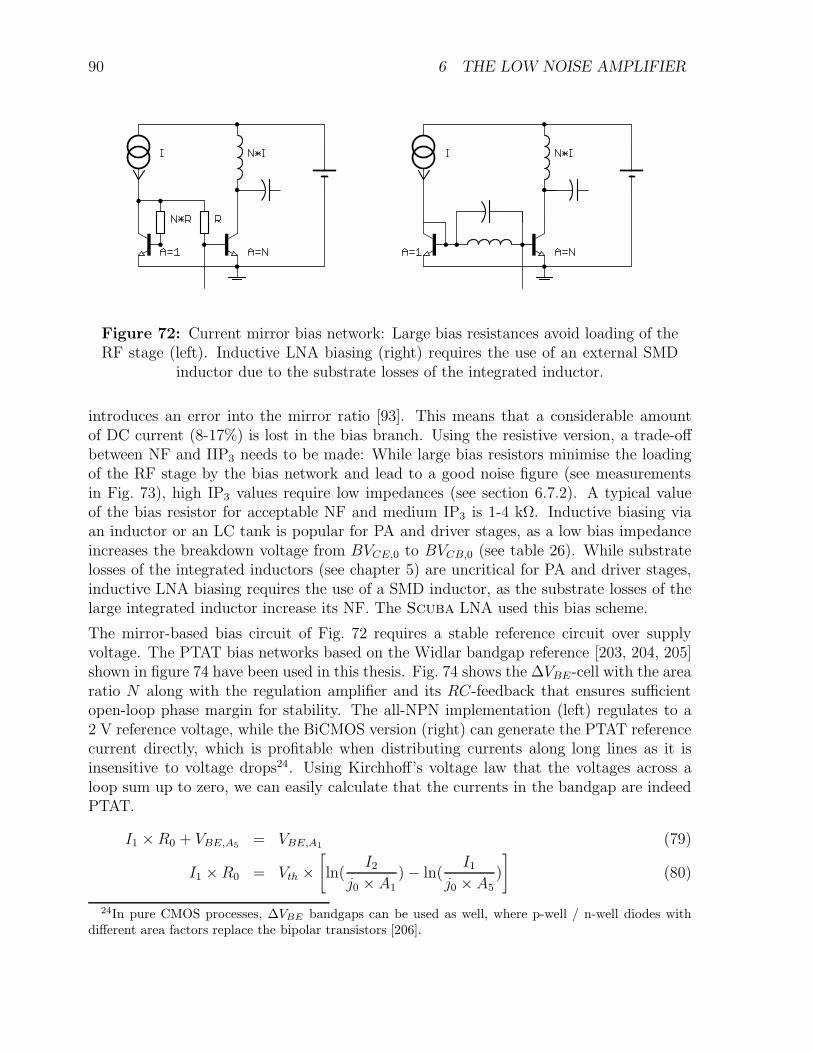
90 6 THE LOW NOISE AMPLIFIER
Figure 72: Current mirror bias network: Large bias resistances avoid loading of theRF stage (left). Inductive LNA biasing (right) requires the use of an external SMD
inductor due to the substrate losses of the integrated inductor.
introduces an error into the mirror ratio [93]. This means that a considerable amountof DC current (8-17%) is lost in the bias branch. Using the resistive version, a trade-offbetween NF and IIP3 needs to be made: While large bias resistors minimise the loadingof the RF stage by the bias network and lead to a good noise figure (see measurementsin Fig. 73), high IP3 values require low impedances (see section 6.7.2). A typical valueof the bias resistor for acceptable NF and medium IP3 is 1-4 kΩ. Inductive biasing viaan inductor or an LC tank is popular for PA and driver stages, as a low bias impedanceincreases the breakdown voltage from BVCE,0 to BVCB,0 (see table 26). While substratelosses of the integrated inductors (see chapter 5) are uncritical for PA and driver stages,inductive LNA biasing requires the use of a SMD inductor, as the substrate losses of thelarge integrated inductor increase its NF. The Scuba LNA used this bias scheme.
The mirror-based bias circuit of Fig. 72 requires a stable reference circuit over supplyvoltage. The PTAT bias networks based on the Widlar bandgap reference [203, 204, 205]shown in figure 74 have been used in this thesis. Fig. 74 shows the ∆VBE-cell with the arearatio N along with the regulation amplifier and its RC-feedback that ensures sufficientopen-loop phase margin for stability. The all-NPN implementation (left) regulates to a2 V reference voltage, while the BiCMOS version (right) can generate the PTAT referencecurrent directly, which is profitable when distributing currents along long lines as it isinsensitive to voltage drops24. Using Kirchhoff’s voltage law that the voltages across aloop sum up to zero, we can easily calculate that the currents in the bandgap are indeedPTAT.
I1 × R0 + VBE,A5= VBE,A1
(79)
I1 × R0 = Vth ×[
ln(I2
j0 × A1) − ln(
I1
j0 × A5)
]
(80)
24In pure CMOS processes, ∆VBE bandgaps can be used as well, where p-well / n-well diodes withdifferent area factors replace the bipolar transistors [206].
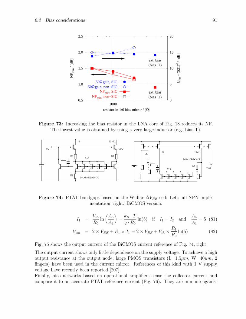
6.4 Bias considerations 91
0.5
1.0
1.5
2.0
2.5
10000
5
10
15
20
NF m
in /
[dB
]
G50
= (
S21)
2 / [d
B]
resistor in 1:6 bias mirror / [Ω]
ext. bias(bias−T)
ext. bias(bias−T)
50Ω gain, SIC50Ω gain, non−SIC
NFmin, SICNFmin, non−SIC
Figure 73: Increasing the bias resistor in the LNA core of Fig. 18 reduces its NF.The lowest value is obtained by using a very large inductor (e.g. bias-T).
Figure 74: PTAT bandgaps based on the Widlar ∆VBE-cell: Left: all-NPN imple-mentation, right: BiCMOS version.
I1 =Vth
R0ln(
A5
A1
)
=kB · Tq · R0
ln(5) if I1 = I2 andA5
A1= 5 (81)
Vout = 2 × VBE + R1 × I1 = 2 × VBE + Vth ×R1
R0ln(5) (82)
Fig. 75 shows the output current of the BiCMOS current reference of Fig. 74, right.
The output current shows only little dependence on the supply voltage. To achieve a highoutput resistance at the output node, large PMOS transistors (L=1.5µm, W=40µm, 2fingers) have been used in the current mirror. References of this kind with 1 V supplyvoltage have recently been reported [207].Finally, bias networks based on operational amplifiers sense the collector current andcompare it to an accurate PTAT reference current (Fig. 76). They are immune against
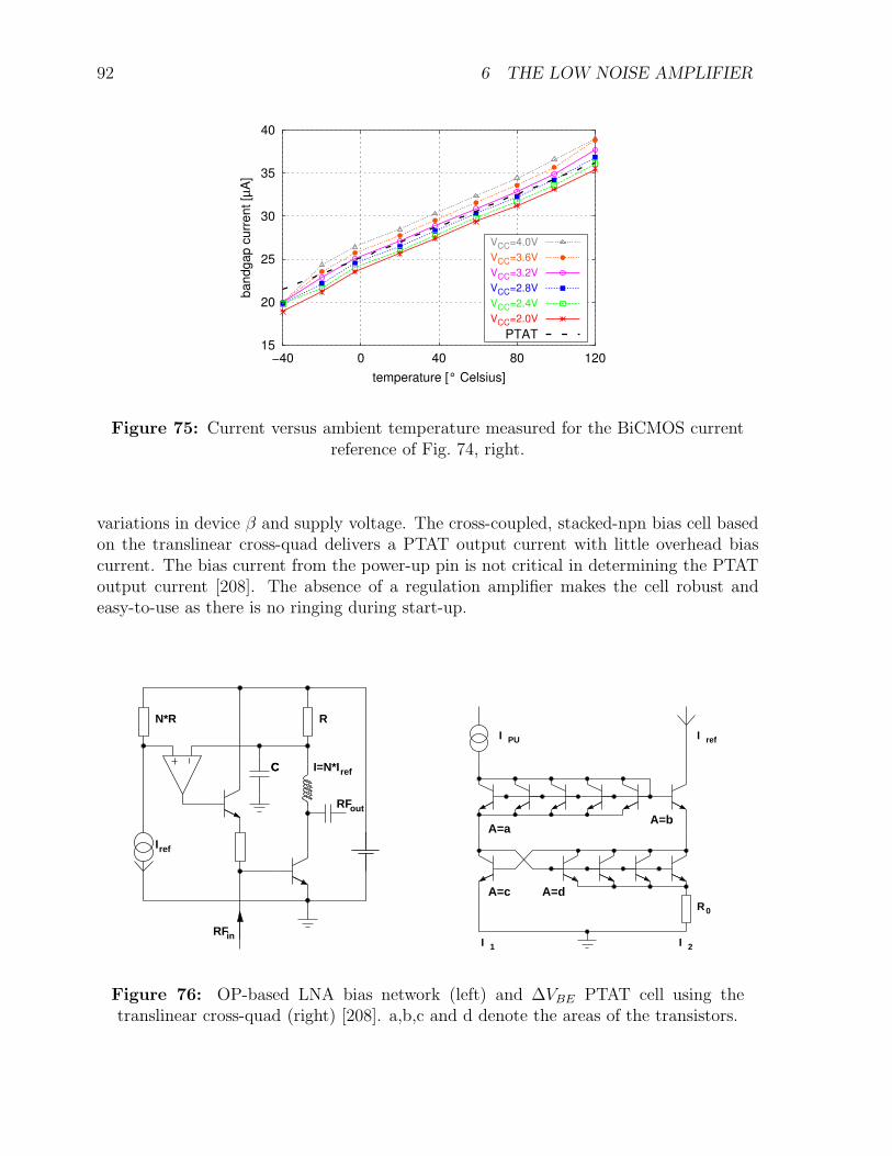
92 6 THE LOW NOISE AMPLIFIER
15
20
25
30
35
40
−40 0 40 80 120
bandgap c
urr
ent [µ
A]
temperature [° Celsius]
VCC=4.0V
VCC=3.6V
VCC=3.2V
VCC=2.8V
VCC=2.4V
VCC=2.0V
PTAT
Figure 75: Current versus ambient temperature measured for the BiCMOS currentreference of Fig. 74, right.
variations in device β and supply voltage. The cross-coupled, stacked-npn bias cell basedon the translinear cross-quad delivers a PTAT output current with little overhead biascurrent. The bias current from the power-up pin is not critical in determining the PTAToutput current [208]. The absence of a regulation amplifier makes the cell robust andeasy-to-use as there is no ringing during start-up.
N*R R
CC
RFout
I=N*I
RFin
Iref
ref
R0
I 2I 1
I PU
A=aA=b
A=dA=c
I ref
Figure 76: OP-based LNA bias network (left) and ∆VBE PTAT cell using thetranslinear cross-quad (right) [208]. a,b,c and d denote the areas of the transistors.
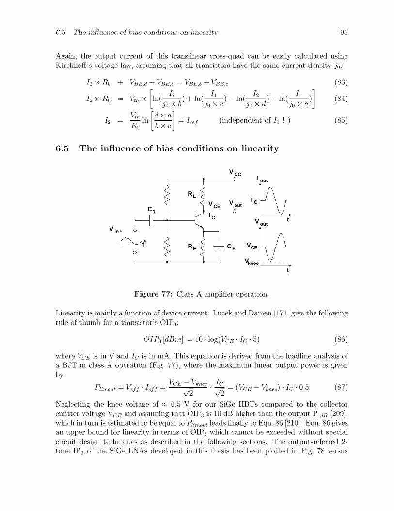
6.5 The influence of bias conditions on linearity 93
Again, the output current of this translinear cross-quad can be easily calculated usingKirchhoff’s voltage law, assuming that all transistors have the same current density j0:
I2 × R0 + VBE,d + VBE,a = VBE,b + VBE,c (83)
I2 × R0 = Vth ×[
ln(I2
j0 × b) + ln(
I1
j0 × c) − ln(
I2
j0 × d) − ln(
I1
j0 × a)
]
(84)
I2 =Vth
R0
ln
[
d × a
b × c
]
= Iref (independent of I1 ! ) (85)
6.5 The influence of bias conditions on linearity
C1
CERE
RL
V in
t
V CEV out
V CC
V out
CI
I C t
t
outI
kneeV
VCE
Figure 77: Class A amplifier operation.
Linearity is mainly a function of device current. Lucek and Damen [171] give the followingrule of thumb for a transistor’s OIP3:
OIP3 [dBm] = 10 · log(VCE · IC · 5) (86)
where VCE is in V and IC is in mA. This equation is derived from the loadline analysis ofa BJT in class A operation (Fig. 77), where the maximum linear output power is givenby
Plin,out = Veff · Ieff =VCE − Vknee√
2· IC√
2= (VCE − Vknee) · IC · 0.5 (87)
Neglecting the knee voltage of ≈ 0.5 V for our SiGe HBTs compared to the collectoremitter voltage VCE and assuming that OIP3 is 10 dB higher than the output P1dB [209],which in turn is estimated to be equal to Plin,out leads finally to Eqn. 86 [210]. Eqn. 86 givesan upper bound for linearity in terms of OIP3 which cannot be exceeded without specialcircuit design techniques as described in the following sections. The output-referred 2-tone IP3 of the SiGe LNAs developed in this thesis has been plotted in Fig. 78 versus
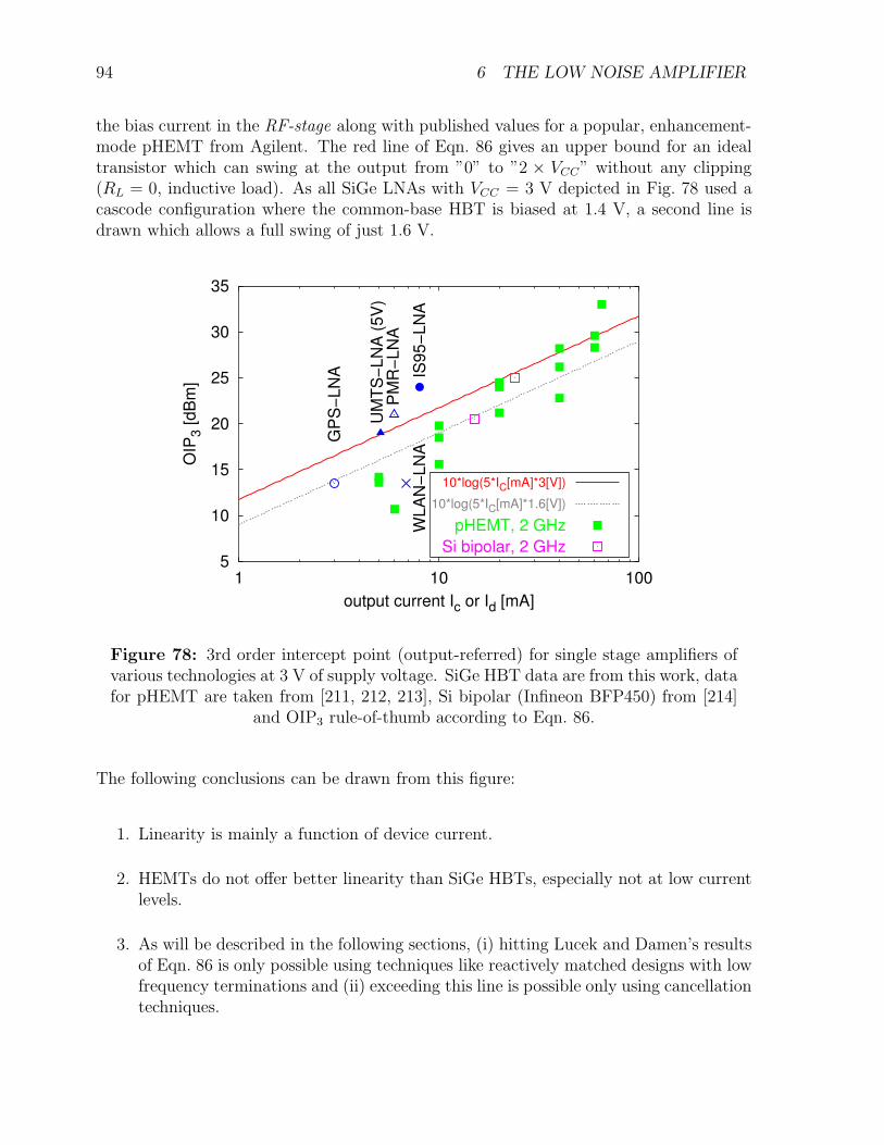
94 6 THE LOW NOISE AMPLIFIER
the bias current in the RF-stage along with published values for a popular, enhancement-mode pHEMT from Agilent. The red line of Eqn. 86 gives an upper bound for an idealtransistor which can swing at the output from ”0” to ”2 × VCC” without any clipping(RL = 0, inductive load). As all SiGe LNAs with VCC = 3 V depicted in Fig. 78 used acascode configuration where the common-base HBT is biased at 1.4 V, a second line isdrawn which allows a full swing of just 1.6 V.
5
10
15
20
25
30
35
1 10 100
OIP
3 [
dB
m]
output current Ic or Id [mA]
GP
S−
LN
A
UM
TS
−L
NA
(5
V)
PM
R−
LN
A
IS9
5−
LN
AW
LA
N−
LN
A
10*log(5*IC[mA]*3[V])
10*log(5*IC[mA]*1.6[V])
pHEMT, 2 GHz
Si bipolar, 2 GHz
Figure 78: 3rd order intercept point (output-referred) for single stage amplifiers ofvarious technologies at 3 V of supply voltage. SiGe HBT data are from this work, datafor pHEMT are taken from [211, 212, 213], Si bipolar (Infineon BFP450) from [214]
and OIP3 rule-of-thumb according to Eqn. 86.
The following conclusions can be drawn from this figure:
1. Linearity is mainly a function of device current.
2. HEMTs do not offer better linearity than SiGe HBTs, especially not at low currentlevels.
3. As will be described in the following sections, (i) hitting Lucek and Damen’s resultsof Eqn. 86 is only possible using techniques like reactively matched designs with lowfrequency terminations and (ii) exceeding this line is possible only using cancellationtechniques.
6.6 Effect of series and parallel feedback on noise figure and linearity 95
6.6 Effect of series and parallel feedback on noise figure andlinearity
As has been explained in section 6.3, the use of series feedback is mandatory to achievenoise and power match simultaneously. In addition, gain is decreased and linearity interms of input-referred intercept point IIP3 is increased. As can be seen in Fig. 78 andfrom Eqn. 86, output-referred linearity is mainly a function of the total device current [215]and cannot strongly be influenced by feedback. While inductive series feedback is usedin most LNA designs, parallel feedback from collector to base is usually not used due tothe following reasons: According to Eqn. 61, parallel feedback decreases reverse isolation leading to LO
feedthrough from the mixer to the antenna25. This is especially unacceptable indirect conversion receivers, as it leads to DC offset at the mixer output. In addition,the stability is decreased. LNAs with large values of S12 show strong dependence of the input match ΓS on theoutput match ΓL as ΓS = S11 + S12·S21·ΓL
1−S22·ΓL. Unilateral LNAs with S12=0 are easy to
match, as ΓS = S11, independent from the output reflection coefficient ΓL and viceversa. Twoports with strong parallel feedback, however, are extremely difficult tomatch as the output matching network has influence on the input matching networkwhich, in turn, depends on the output match. Resistive parallel feedback as shown in Figs. 63 or 133 has detrimental effects onnoise figure, if the feedback resistance is low.
Iversen in 1974 [216] derived the theoretical formulae which describe the influence ofparallel and series feedback on the noise figure of a twoport and and Boglione [217] et al.for the equivalent noise resistance Rn. As the formulae are rather involved and difficultto apply to feedback elements with parasitic networks (e.g. MIM capacitors), the effectof a MIM feedback capacitor has been measured at 2 GHz using versions of the LNA coreshown in Fig. 18 with different feedback capacitor (no emitter degeneration):
As expected, the gain decreases strongly with increasing feedback, but the minimum noisefigure remains constant. No reduction of the noise figure due capacitive feedback has beenobserved, as proposed by Cooke [218] for a common-emitter stage26. As has been shown
25This is not the case for ideal series feedback: The S-parameters for series emitter feedback withresistor Re can be obtained from Eqns. 56-61 by setting Rfb = ∞ and replacing gm = IC/Vth bythe transconductance of the emitter degenerated BJT, which is gm,sf = gm/(1 + gm · Re). This wayS11 = 1, S22 = (Rl −Z0)/(Rl +Z0), S21 = −2 · gm,sf ·Rl ·Z0/(Rl +Z0) and S12 = 0. Rollet’s k is infiniteand ∆ = S22 < 1. This means the ideal BJT amplifier with emitter series feedback has infinite reverseisolation and is unconditionally stable.
26Cooke points out, however, that the noise measure M = G · (F − 1)/(G − 1) [219], where G is gainand F is noise factor remains constant.
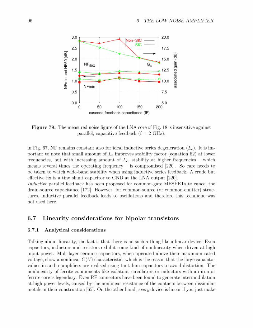
96 6 THE LOW NOISE AMPLIFIER
0.0
0.5
1.0
1.5
2.0
2.5
3.0
0 50 100 150 2005.0
7.5
10.0
12.5
15.0
17.5
20.0
NF
min
an
d N
F5
0 [
dB
]
asso
cia
ted
ga
in (
dB
)
cascode feedback capacitance (fF)
NFmin
NF50Ω Ga
Non−SICSIC
Figure 79: The measured noise figure of the LNA core of Fig. 18 is insensitive againstparallel, capacitive feedback (f = 2 GHz).
in Fig. 67, NF remains constant also for ideal inductive series degeneration (Le). It is im-portant to note that small amount of Le improves stability factor (equation 62) at lowerfrequencies, but with increasing amount of Le, stability at higher frequencies – whichmeans several times the operating frequency – is compromised [220]. So care needs tobe taken to watch wide-band stability when using inductive series feedback. A crude buteffective fix is a tiny shunt capacitor to GND at the LNA output [220].Inductive parallel feedback has been proposed for common-gate MESFETs to cancel thedrain-source capacitance [172]. However, for common-source (or common-emitter) struc-tures, inductive parallel feedback leads to oscillations and therefore this technique wasnot used here.
6.7 Linearity considerations for bipolar transistors
6.7.1 Analytical considerations
Talking about linearity, the fact is that there is no such a thing like a linear device: Evencapacitors, inductors and resistors exhibit some kind of nonlinearity when driven at highinput power. Multilayer ceramic capacitors, when operated above their maximum ratedvoltage, show a nonlinear C(U) characteristic, which is the reason that the large capacitorvalues in audio amplifiers are realised using tantalum capacitors to avoid distortion. Thenonlinearity of ferrite components like isolators, circulators or inductors with an iron orferrite core is legendary. Even RF connectors have been found to generate intermodulationat high power levels, caused by the nonlinear resistance of the contacts between dissimilarmetals in their construction [65]. On the other hand, every device is linear if you just make
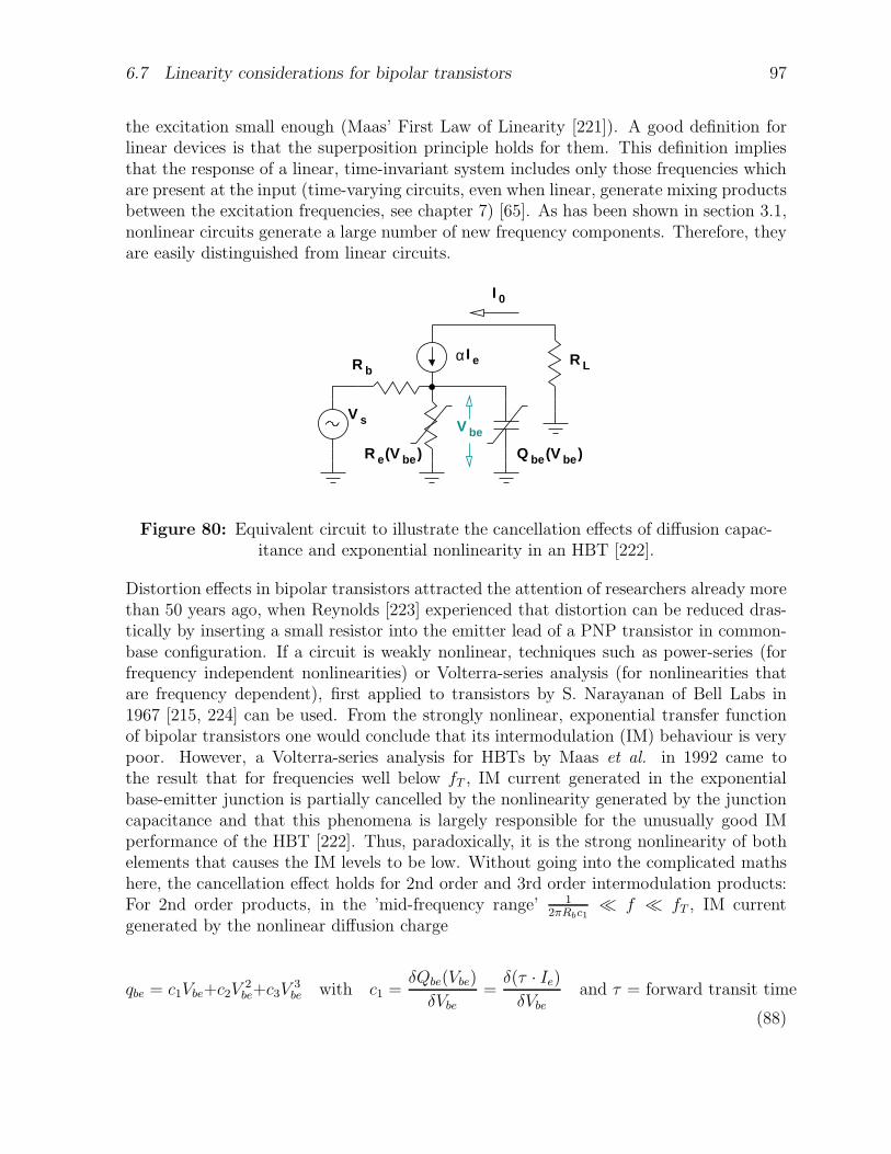
6.7 Linearity considerations for bipolar transistors 97
the excitation small enough (Maas’ First Law of Linearity [221]). A good definition forlinear devices is that the superposition principle holds for them. This definition impliesthat the response of a linear, time-invariant system includes only those frequencies whichare present at the input (time-varying circuits, even when linear, generate mixing productsbetween the excitation frequencies, see chapter 7) [65]. As has been shown in section 3.1,nonlinear circuits generate a large number of new frequency components. Therefore, theyare easily distinguished from linear circuits.
R L
I 0
R b
V s V be
R e ) Q be (V be
I eα
(V be )
Figure 80: Equivalent circuit to illustrate the cancellation effects of diffusion capac-itance and exponential nonlinearity in an HBT [222].
Distortion effects in bipolar transistors attracted the attention of researchers already morethan 50 years ago, when Reynolds [223] experienced that distortion can be reduced dras-tically by inserting a small resistor into the emitter lead of a PNP transistor in common-base configuration. If a circuit is weakly nonlinear, techniques such as power-series (forfrequency independent nonlinearities) or Volterra-series analysis (for nonlinearities thatare frequency dependent), first applied to transistors by S. Narayanan of Bell Labs in1967 [215, 224] can be used. From the strongly nonlinear, exponential transfer functionof bipolar transistors one would conclude that its intermodulation (IM) behaviour is verypoor. However, a Volterra-series analysis for HBTs by Maas et al. in 1992 came tothe result that for frequencies well below fT , IM current generated in the exponentialbase-emitter junction is partially cancelled by the nonlinearity generated by the junctioncapacitance and that this phenomena is largely responsible for the unusually good IMperformance of the HBT [222]. Thus, paradoxically, it is the strong nonlinearity of bothelements that causes the IM levels to be low. Without going into the complicated mathshere, the cancellation effect holds for 2nd order and 3rd order intermodulation products:For 2nd order products, in the ’mid-frequency range’ 1
2πRbc1 f fT , IM current
generated by the nonlinear diffusion charge
qbe = c1Vbe+c2V2be+c3V
3be with c1 =
δQbe(Vbe)
δVbe=
δ(τ · Ie)
δVbeand τ = forward transit time
(88)
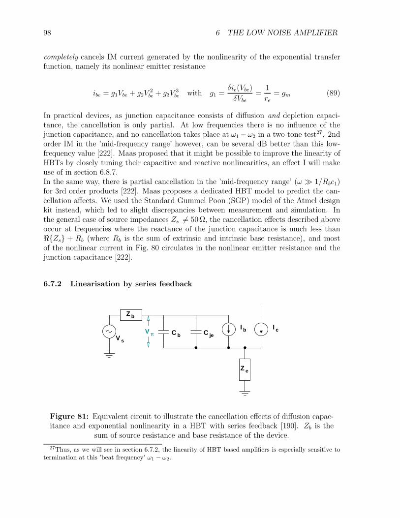
98 6 THE LOW NOISE AMPLIFIER
completely cancels IM current generated by the nonlinearity of the exponential transferfunction, namely its nonlinear emitter resistance
ibe = g1Vbe + g2V2be + g3V
3be with g1 =
δie(Vbe)
δVbe
=1
re
= gm (89)
In practical devices, as junction capacitance consists of diffusion and depletion capaci-tance, the cancellation is only partial. At low frequencies there is no influence of thejunction capacitance, and no cancellation takes place at ω1 −ω2 in a two-tone test27. 2ndorder IM in the ’mid-frequency range’ however, can be several dB better than this low-frequency value [222]. Maas proposed that it might be possible to improve the linearity ofHBTs by closely tuning their capacitive and reactive nonlinearities, an effect I will makeuse of in section 6.8.7.In the same way, there is partial cancellation in the ’mid-frequency range’ (ω 1/Rbc1)for 3rd order products [222]. Maas proposes a dedicated HBT model to predict the can-cellation affects. We used the Standard Gummel Poon (SGP) model of the Atmel designkit instead, which led to slight discrepancies between measurement and simulation. Inthe general case of source impedances Zs 6= 50 Ω, the cancellation effects described aboveoccur at frequencies where the reactance of the junction capacitance is much less than<Zs + Rb (where Rb is the sum of extrinsic and intrinsic base resistance), and mostof the nonlinear current in Fig. 80 circulates in the nonlinear emitter resistance and thejunction capacitance [222].
6.7.2 Linearisation by series feedback
Z b
V πV s
I b I cC b C je
Z e
Figure 81: Equivalent circuit to illustrate the cancellation effects of diffusion capac-itance and exponential nonlinearity in a HBT with series feedback [190]. Zb is the
sum of source resistance and base resistance of the device.
27Thus, as we will see in section 6.7.2, the linearity of HBT based amplifiers is especially sensitive totermination at this ’beat frequency’ ω1 − ω2.
6.7 Linearity considerations for bipolar transistors 99
As shown in section 6.6, there is no negative effect of parallel capacitive or series inductivefeedback on the noise behaviour. It does have, however, a big impact on linearity: In 1998,Fong and Meyer [190] extended Maas’ approach and applied a Volterra-series analysis totransconductance stages, degenerated with series feedback (see Fig. 81):
Ic = A1(s) · Vs + A2(s1, s2) · V 2s + A3(s1, s2, s3) · V 3
s (90)
V ns is the nth power of the voltage source signal, An() is the Volterra series coefficient,
which is a linear function of n number of frequencies and s = j · ω the Laplace variable.Complicated calculations [190] using Ic = IQ exp (Vπ/Vth) – where IQ is the saturationcurrent of the HBT – and Ib = Ic/β0 lead to A1(s), A2(s1, s2) and A3(s1, s2, s3), whereA1(s) is the small signal transconductance of the common-emitter stage:
A1(s) =gm
[s · Cje · Z(s) + s · τF · gm · Z(s) + gm · Z(s)/β0 + 1 + gm · Ze(s)](91)
with Z(s) = Zb(s) + Ze(s) and gm = IQ/Vth (transconductance of the transistor withoutfeedback). The IM3 product at frequency (2ωa−ωb) can be calculated by using the Volterraseries coefficient A3(s1, s2, s3) and letting s1 = sa, s2 = sa and s3 = −sb. Typically thefrequency difference between ωa and ωb is small and s ≈ sa ≈ sb. Using two input signalsof the same amplitude Vs, the magnitude of the input-referred IM3 products (not to beconfused with the intermodulation distance between fundamental and IM3) is given by
|IM3| =
∣∣∣∣
3
4
A3(sa, sa,−sb)
A1(2sa − sb)
∣∣∣∣|Vs|2
≈∣∣∣∣
A1(s)
IQ
∣∣∣∣
3
∣∣∣∣∣∣
Vth
4[1 + sCjeZ(s)] ×
−1 +
A1(∆s)
gm
[1 + ∆sCjeZ(∆s)︸ ︷︷ ︸
≈0
] +A1(2s)
2gm
[1 + 2sCjeZ(2s)]
∣∣∣∣∣∣
|Vs|2
≈∣∣∣∣
A1(s)
IQ
∣∣∣∣
3
∣∣∣∣∣∣∣∣∣
Vth
4
1 + sCjeZ(s)
︸ ︷︷ ︸
deg.
×
−1︸︷︷︸
3rd order
+A1(∆s)
gm
+A1(2s)
2gm
[1 + 2sCjeZ(2s)]
︸ ︷︷ ︸
2nd order
∣∣∣∣∣∣∣∣∣
|Vs|2 (92)
As can be seen directly 3rd order intermodulation products are proportional to the cube of the ratio ofsmall-signal transconductance A1(s) to collector current IQ. A1(s) increases withcollector current IQ, but – depending on the feedback Ze and the base impedanceZb – always with a slope below IQ (see Eqn. 91). Raising the collector current istherefore the most efficient means to improve 3rd order linearity. Using inductive degeneration, [s · Cje · Ze(s)] is a negative real number and cancelsthe ’1’ term partially. There is no such cancellation with resistive degeneration.Thus, common-emitter stages using series inductive degeneration are more linearthan those using capacitive or resistive degeneration with the same transconductanceand bias current [190].
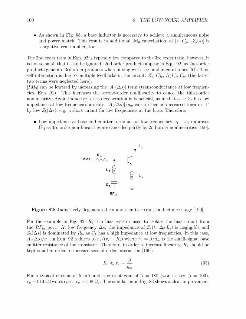
100 6 THE LOW NOISE AMPLIFIER As shown in Fig. 68, a base inductor is necessary to achieve a simultaneous noiseand power match. This results in additional IM3 cancellation, as [s · Cje · Zb(s)] isa negative real number, too.
The 2nd order term in Eqn. 92 is typically low compared to the 3rd order term, however, itis not so small that it can be ignored. 2nd order products appear in Eqn. 92, as 2nd-orderproducts generate 3rd order products when mixing with the fundamental tones [61]. Thisself-interaction is due to multiple feedbacks in the circuit: Ze, Cje, Ib(Ic), Cbc (the lattertwo terms were neglected here).|IM3| can be lowered by increasing the |A1(∆s)| term (transconductance at low frequen-cies, Eqn. 91). This increases the second-order nonlinearity to cancel the third-ordernonlinearity. Again inductive series degeneration is beneficial, as in that case Ze has lowimpedance at low frequencies already. |A1(∆s)|/gm can further be increased towards ’1’by low Zb(∆s), e.g. a short circuit for low frequencies at the base. Therefore: Low impedance at base and emitter terminals at low frequencies ω1 − ω2 improves
IP3 as 3rd order non-linearities are cancelled partly by 2nd-order nonlinearities [190].
I c
Rb
L 1
C1
L e
inRF
Bias
Figure 82: Inductively degenerated common-emitter transconductance stage [190].
For the example in Fig. 82, Rb is a bias resistor used to isolate the bias circuit fromthe RFin port. At low frequency ∆s, the impedance of Ze(≈ ∆s Le) is negligible andZb(∆s) is dominated by Rb, as C1 has a high impedance at low frequencies. In this case,A1(∆s)/gm in Eqn. 92 reduces to rπ/(rπ + Rb) where rπ = β/gm is the small-signal baseemitter resistance of the transistor. Therefore, in order to increase linearity, Rb should bekept small in order to increase second-order interaction [190]:
Rb rπ =β
gm
(93)
For a typical current of 5 mA and a current gain of β = 180 (worst case: β = 100),rπ = 914 Ω (worst case: rπ = 508 Ω). The simulation in Fig. 83 shows a clear improvement
6.7 Linearity considerations for bipolar transistors 101
if the bias resistor is well below this value. On the other hand, reducing the bias resistor Rb
considerably below rπ leads to a large increase in NF (verified experimentally in Fig. 73).Thus, in this simple design a compromise between NF and IP3 is necessary.In the same way Fong and Meyer calculated a Volterra series expansion for a degenerateddifferential pair [190] and came to the conclusion that
1. inductively degenerated differential pairs are more linear than resistively or capaci-tively degenerated differential pairs
2. the IM3 products for the differential pair are at least twice as large as the IM3 prod-ucts of the single common-emitter stage for the same bias current and transconduc-tance. Single-ended common-emitter stages are therefore more linear than differential-pair stages with the same bias current and transconductance.
3. there is no influence of low frequency base or emitter termination on IM3.
Thus, a common-emitter transconductance stage can be biased at a lower current than adifferential-pair transconductance stage with the same linearity and transconductance [190].Therefore, in this thesis, no LNAs based on differential pairs have been realised. SimilarVolterra analysis for bipolar transistors and HBTs can be found in [65, 61, 225].As Fong’s and Meyer’s computations neglected the base-collector capacitance Cbc (whichwas not done in [61]), their results are even more valid for cascode configurations.The effect of low-frequency termination on the intermodulation performance of a TXdriver amp has been studied in [226]. Aparin and Persico in 1999 presented a bipolarLNA with exceptional high linearity [61]. Their analysis revealed that shorting the baseat ω1 − ω2 improves IIP3, but the optimum value for the termination impedance is 6= 0.Such optimum nonzero sub-harmonic termination fixes the amplitude and phase of themodulation signal appearing in the bias circuit so that the product of its mixing with theinput signal cancels the remaining IM3 terms [61]. In addition, out-of-band terminationat ω1 + ω2 – in PAs used to optimise power-added-efficiency – can lead to complete can-cellation of 2nd and 3rd order contributions leading to very high IM3. As we will see insection 6.8.7, this is very tricky and works only for amplifiers which need to operate in avery narrow frequency band.In 2002 van der Heijden, de Graaff and de Vreede reported a balanced LNA with an OIP3
of 20 dBm with just 2mA of bias current [227]. Again this was achieved by controlling the2nd harmonic at the output. The result was extremely sensitive to tone-spacing, however.It is interesting to note that low-frequency termination and harmonic termination does notseem to have an effect on the intermodulation performance of MOS and HEMT devices:Simulation results using HEMTs showed constant IIP3 for different bias terminations.This is obviously due to the missing cancellation between 2nd and 3rd order products.
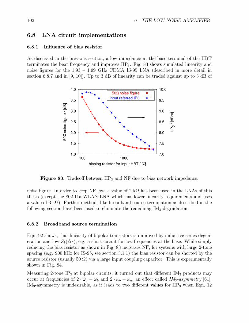
102 6 THE LOW NOISE AMPLIFIER
6.8 LNA circuit implementations
6.8.1 Influence of bias resistor
As discussed in the previous section, a low impedance at the base terminal of the HBTterminates the beat frequency and improves IIP3. Fig. 83 shows simulated linearity andnoise figures for the 1.93 – 1.99 GHz CDMA IS-95 LNA (described in more detail insection 6.8.7 and in [9, 10]). Up to 3 dB of linearity can be traded against up to 3 dB of
1.0
1.5
2.0
2.5
3.0
3.5
4.0
100 10007.0
7.5
8.0
8.5
9.0
9.5
10.0
50
Ω n
ois
e f
igu
re /
[d
B]
IIP
3 /
[d
Bm
]
biasing resistor for input HBT / [Ω]
50Ω noise figure
input referred IP3
Figure 83: Tradeoff between IIP3 and NF due to bias network impedance.
noise figure. In order to keep NF low, a value of 2 kΩ has been used in the LNAs of thisthesis (except the 802.11a WLAN LNA which has lower linearity requirements and usesa value of 3 kΩ). Further methods like broadband source termination as described in thefollowing section have been used to eliminate the remaining IM3 degradation.
6.8.2 Broadband source termination
Eqn. 92 shows, that linearity of bipolar transistors is improved by inductive series degen-eration and low Zb(∆s), e.g. a short circuit for low frequencies at the base. While simplyreducing the bias resistor as shown in Fig. 83 increases NF, for systems with large 2-tonespacing (e.g. 900 kHz for IS-95, see section 3.1.1) the bias resistor can be shorted by thesource resistor (usually 50 Ω) via a large input coupling capacitor. This is experimentallyshown in Fig. 84.
Measuring 2-tone IP3 at bipolar circuits, it turned out that different IM3 products mayoccur at frequencies of 2 · ωa − ωb and 2 · ωb − ωa, an effect called IM3-asymmetry [61].IM3-asymmetry is undesirable, as it leads to two different values for IIP3 when Eqn. 12
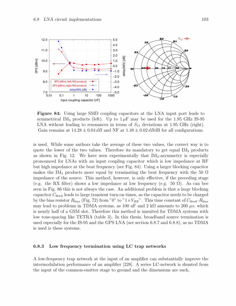
6.8 LNA circuit implementations 103
7.0
8.0
9.0
10.0
11.0
12.0
0.01 0.1 1 10 100 1000−5.0
−4.0
−3.0
−2.0
−1.0
0.0
1.0
2.0
3.0
4.0
5.0IIP
3 [dB
m]
delta(I
M3)
[dB
]
input coupling capacitor [nF]
IIP3 [dBm] (left IM3 product)
IIP3 [dBm] (right IM3 product)
delta(IM3) [dB]
j0.3
j0.6
j1.0j1.5
j3.0
−j0.3
−j0.6
−j1.0−j1.5
−j3.0
0.15 0.3 0.6 1.0 1.5 3.00.0 8
j0.3
j0.6
j1.0j1.5
j3.0
−j0.3
−j0.6
−j1.0−j1.5
−j3.0
0.15 0.3 0.6 1.0 1.5 3.00.0 8
j0.3
j0.6
j1.0j1.5
j3.0
−j0.3
−j0.6
−j1.0−j1.5
−j3.0
0.15 0.3 0.6 1.0 1.5 3.00.0 8
j0.3
j0.6
j1.0j1.5
j3.0
−j0.3
−j0.6
−j1.0−j1.5
−j3.0
0.15 0.3 0.6 1.0 1.5 3.00.0 8
j0.3
j0.6
j1.0j1.5
j3.0
−j0.3
−j0.6
−j1.0−j1.5
−j3.0
0.15 0.3 0.6 1.0 1.5 3.00.0 8
j0.3
j0.6
j1.0j1.5
j3.0
−j0.3
−j0.6
−j1.0−j1.5
−j3.0
0.15 0.3 0.6 1.0 1.5 3.00.0 8
j0.3
j0.6
j1.0j1.5
j3.0
−j0.3
−j0.6
−j1.0−j1.5
−j3.0
0.15 0.3 0.6 1.0 1.5 3.00.0 8
j0.3
j0.6
j1.0j1.5
j3.0
−j0.3
−j0.6
−j1.0−j1.5
−j3.0
0.15 0.3 0.6 1.0 1.5 3.00.0 8
j0.3
j0.6
j1.0j1.5
j3.0
−j0.3
−j0.6
−j1.0−j1.5
−j3.0
0.15 0.3 0.6 1.0 1.5 3.00.0 8
j0.3
j0.6
j1.0j1.5
j3.0
−j0.3
−j0.6
−j1.0−j1.5
−j3.0
0.15 0.3 0.6 1.0 1.5 3.00.0 8
j0.3
j0.6
j1.0j1.5
j3.0
−j0.3
−j0.6
−j1.0−j1.5
−j3.0
0.15 0.3 0.6 1.0 1.5 3.00.0 8
j0.3
j0.6
j1.0j1.5
j3.0
−j0.3
−j0.6
−j1.0−j1.5
−j3.0
0.15 0.3 0.6 1.0 1.5 3.00.0 8
j0.3
j0.6
j1.0j1.5
j3.0
−j0.3
−j0.6
−j1.0−j1.5
−j3.0
0.15 0.3 0.6 1.0 1.5 3.00.0 8
j0.3
j0.6
j1.0j1.5
j3.0
−j0.3
−j0.6
−j1.0−j1.5
−j3.0
0.15 0.3 0.6 1.0 1.5 3.00.0 8
j0.3
j0.6
j1.0j1.5
j3.0
−j0.3
−j0.6
−j1.0−j1.5
−j3.0
0.15 0.3 0.6 1.0 1.5 3.00.0 8
j0.3
j0.6
j1.0j1.5
j3.0
−j0.3
−j0.6
−j1.0−j1.5
−j3.0
0.15 0.3 0.6 1.0 1.5 3.00.0 8
j0.3
j0.6
j1.0j1.5
j3.0
−j0.3
−j0.6
−j1.0−j1.5
−j3.0
0.15 0.3 0.6 1.0 1.5 3.00.0 8
j0.3
j0.6
j1.0j1.5
j3.0
−j0.3
−j0.6
−j1.0−j1.5
−j3.0
0.15 0.3 0.6 1.0 1.5 3.00.0 8
j0.3
j0.6
j1.0j1.5
j3.0
−j0.3
−j0.6
−j1.0−j1.5
−j3.0
0.15 0.3 0.6 1.0 1.5 3.00.0 8
S11
Figure 84: Using large SMD coupling capacitors at the LNA input port leads tosymmetrical IM3 products (left). Up to 1 µF may be used for the 1.95 GHz IS-95LNA without leading to resonances in terms of S11 deviations at 1.95 GHz (right).Gain remains at 14.28 ± 0.04 dB and NF at 1.48 ± 0.02 dBdB for all configurations.
is used. While some authors take the average of these two values, the correct way is toquote the lower of the two values. Therefore its mandatory to get equal IM3 productsas shown in Fig. 12. We have seen experimentally that IM3-asymmetry is especiallypronounced for LNAs with an input coupling capacitor which is low impedance at RFbut high impedance at the beat frequency (see Fig. 84). Using a larger blocking capacitormakes the IM3 products more equal by terminating the beat frequency with the 50 Ωimpedance of the source. This method, however, is only effective, if the preceding stage(e.g. the RX filter) shows a low impedance at low frequency (e.g. 50 Ω). As can beeseen in Fig. 86 this is not always the case. An additional problem is that a large blockingcapacitor Cblock leads to large transient turn-on times, as the capacitor needs to be chargedby the bias resistor Rbias (Fig. 72) from ”0” to ”1×VBE”. This time constant of Cblock ·Rbias
may lead to problems in TDMA systems, as 100 nF and 2 kΩ amounts to 200 µs, whichis nearly half of a GSM slot. Therefore this method is unsuited for TDMA systems withlow tone-spacing like TETRA (table 3). In this thesis, broadband source termination isused especially for the IS-95 and the GPS LNA (see section 6.8.7 and 6.8.8), as no TDMAis used is these systems.
6.8.3 Low frequency termination using LC trap networks
A low-frequency trap network at the input of an amplifier can substantially improve theintermodulation performance of an amplifier [228]. A series LC-network is shunted fromthe input of the common-emitter stage to ground and the dimensions are such,
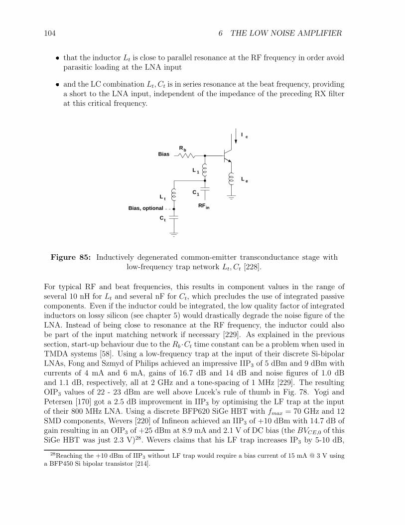
104 6 THE LOW NOISE AMPLIFIER that the inductor Lt is close to parallel resonance at the RF frequency in order avoidparasitic loading at the LNA input and the LC combination Lt, Ct is in series resonance at the beat frequency, providinga short to the LNA input, independent of the impedance of the preceding RX filterat this critical frequency.
I c
Rb
L 1
C1
L e
L t
C t
inRF
Bias
Bias, optional
Figure 85: Inductively degenerated common-emitter transconductance stage withlow-frequency trap network Lt, Ct [228].
For typical RF and beat frequencies, this results in component values in the range ofseveral 10 nH for Lt and several nF for Ct, which precludes the use of integrated passivecomponents. Even if the inductor could be integrated, the low quality factor of integratedinductors on lossy silicon (see chapter 5) would drastically degrade the noise figure of theLNA. Instead of being close to resonance at the RF frequency, the inductor could alsobe part of the input matching network if necessary [229]. As explained in the previoussection, start-up behaviour due to the Rb ·Ct time constant can be a problem when used inTMDA systems [58]. Using a low-frequency trap at the input of their discrete Si-bipolarLNAs, Fong and Szmyd of Philips achieved an impressive IIP3 of 5 dBm and 9 dBm withcurrents of 4 mA and 6 mA, gains of 16.7 dB and 14 dB and noise figures of 1.0 dBand 1.1 dB, respectively, all at 2 GHz and a tone-spacing of 1 MHz [229]. The resultingOIP3 values of 22 - 23 dBm are well above Lucek’s rule of thumb in Fig. 78. Yogi andPetersen [170] got a 2.5 dB improvement in IIP3 by optimising the LF trap at the inputof their 800 MHz LNA. Using a discrete BFP620 SiGe HBT with fmax = 70 GHz and 12SMD components, Wevers [220] of Infineon achieved an IIP3 of +10 dBm with 14.7 dB ofgain resulting in an OIP3 of +25 dBm at 8.9 mA and 2.1 V of DC bias (the BVCE,0 of thisSiGe HBT was just 2.3 V)28. Wevers claims that his LF trap increases IP3 by 5-10 dB,
28Reaching the +10 dBm of IIP3 without LF trap would require a bias current of 15 mA @ 3 V usinga BFP450 Si bipolar transistor [214].
6.8 LNA circuit implementations 105
while 4 dB seems to be more reasonable when comparing with Fig. 78. Note that shortingthe (f2 − f1) product as done by the LC trap does not increase the compression level ofthe amplifier, just IP3. Using this technique, the general rule of thumb, stating that IIP3
is 10 dB above P1dB is no longer valid. Wevers claims to get a difference of 17.9 dB here.In summary, the disadvantage of this technique is the increase of the bill of materials due tothe two additional SMD components, delays during start-up in TDMA systems [170] andits limitations to test cases where a high IP3 is needed only at a single tone-spacing (likeCDMA-IS95), although a flat IIP3 over 1.5 decades of tone spacing can be achieved (Fig. 5in [220]). However, the drop in IIP3 when the tone spacing approaches ”0” is pronounced,making this technique unsuited for PMR systems with low channel spacing (see table 3).
6.8.4 Low frequency termination using bias inductors and a diode
The modification of the low frequency trap, as applied in this thesis, is the inductivebias network shown in Fig. 72, right [58]: The inductor is operated close to parallelresonance at RF frequencies in order to avoid loading and noise figure degradation of theRF stage. Properly designed, the influence of the bias network on the noise figure canbe eliminated completely, leading to noise figures lower than what can be achieved usingpractical values of bias resistors (see Fig. 73, where the very large inductor of a bias-T wasused for biasing). For low frequencies, the base of the RF transistor is terminated by thedynamic resistance of the biasing diode, which is re = δV /δI = Vth/Idiode. Using an RFcurrent of 6 mA and a mirror ratio of 1:6 . . . 1:12, the current in the diode is 1.0 . . . 0.5 mAresulting in an impedance of 25 . . . 50 Ω which is sufficiently low to terminate the baseproperly (see Eqn. 93). This technique, previously known from the design of TX driveramplifiers and power amplifiers [226]29 provides a broad-band low frequency termination independent of the RX filter
impedance at low frequency and is therefore suited for all kind of systems thatrequire high IP3 values within a wide range of tone spacings (e.g. UMTS) uses only one external SMD inductor due to the absence of large sized SMD capacitors is not prone to delays duringstart-up and yields excellent noise figures as it avoids resistive loading of the input resistor.
For infrastructure parts, the added cost of an external SMD inductor for biasing is notcritical and therefore this technique was used within the Scuba project, where an RXfilter with high impedance at low frequencies (Fig. 86) precedes the LNA.
29While this technique belongs to textbook know-how, Agilent Technologies filed a patent applicationin 2002 for the implementation with enhancement mode FETs [230].
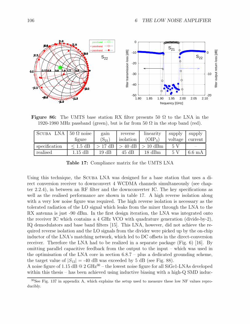
106 6 THE LOW NOISE AMPLIFIER
j0.3
j0.6
j1.0j1.5
j3.0
−j0.3
−j0.6
−j1.0−j1.5
−j3.0
0.15 0.3 0.6 1.0 1.5 3.00.0 8
j0.3
j0.6
j1.0j1.5
j3.0
−j0.3
−j0.6
−j1.0−j1.5
−j3.0
0.15 0.3 0.6 1.0 1.5 3.00.0 8
j0.3
j0.6
j1.0j1.5
j3.0
−j0.3
−j0.6
−j1.0−j1.5
−j3.0
0.15 0.3 0.6 1.0 1.5 3.00.0 8
j0.3
j0.6
j1.0j1.5
j3.0
−j0.3
−j0.6
−j1.0−j1.5
−j3.0
0.15 0.3 0.6 1.0 1.5 3.00.0 8
j0.3
j0.6
j1.0j1.5
j3.0
−j0.3
−j0.6
−j1.0−j1.5
−j3.0
0.15 0.3 0.6 1.0 1.5 3.00.0 8
j0.3
j0.6
j1.0j1.5
j3.0
−j0.3
−j0.6
−j1.0−j1.5
−j3.0
0.15 0.3 0.6 1.0 1.5 3.00.0 8
j0.3
j0.6
j1.0j1.5
j3.0
−j0.3
−j0.6
−j1.0−j1.5
−j3.0
0.15 0.3 0.6 1.0 1.5 3.00.0 8
j0.3
j0.6
j1.0j1.5
j3.0
−j0.3
−j0.6
−j1.0−j1.5
−j3.0
0.15 0.3 0.6 1.0 1.5 3.00.0 8
j0.3
j0.6
j1.0j1.5
j3.0
−j0.3
−j0.6
−j1.0−j1.5
−j3.0
0.15 0.3 0.6 1.0 1.5 3.00.0 8
j0.3
j0.6
j1.0j1.5
j3.0
−j0.3
−j0.6
−j1.0−j1.5
−j3.0
0.15 0.3 0.6 1.0 1.5 3.00.0 8
j0.3
j0.6
j1.0j1.5
j3.0
−j0.3
−j0.6
−j1.0−j1.5
−j3.0
0.15 0.3 0.6 1.0 1.5 3.00.0 8
j0.3
j0.6
j1.0j1.5
j3.0
−j0.3
−j0.6
−j1.0−j1.5
−j3.0
0.15 0.3 0.6 1.0 1.5 3.00.0 8
j0.3
j0.6
j1.0j1.5
j3.0
−j0.3
−j0.6
−j1.0−j1.5
−j3.0
0.15 0.3 0.6 1.0 1.5 3.00.0 8
j0.3
j0.6
j1.0j1.5
j3.0
−j0.3
−j0.6
−j1.0−j1.5
−j3.0
0.15 0.3 0.6 1.0 1.5 3.00.0 8
j0.3
j0.6
j1.0j1.5
j3.0
−j0.3
−j0.6
−j1.0−j1.5
−j3.0
0.15 0.3 0.6 1.0 1.5 3.00.0 8
j0.3
j0.6
j1.0j1.5
j3.0
−j0.3
−j0.6
−j1.0−j1.5
−j3.0
0.15 0.3 0.6 1.0 1.5 3.00.0 8
j0.3
j0.6
j1.0j1.5
j3.0
−j0.3
−j0.6
−j1.0−j1.5
−j3.0
0.15 0.3 0.6 1.0 1.5 3.00.0 8
j0.3
j0.6
j1.0j1.5
j3.0
−j0.3
−j0.6
−j1.0−j1.5
−j3.0
0.15 0.3 0.6 1.0 1.5 3.00.0 8
j0.3
j0.6
j1.0j1.5
j3.0
−j0.3
−j0.6
−j1.0−j1.5
−j3.0
0.15 0.3 0.6 1.0 1.5 3.00.0 8
S22
passband
< passband
> passband
-50
-40
-30
-20
-10
0
1.80 1.85 1.90 1.95 2.00 2.05 2.10-20
-10
0
filte
r tr
ansm
issi
on lo
ss [d
B]
filte
r ou
tput
ret
urn
loss
[dB
]
frequency [GHz]
S21
S22
Figure 86: The UMTS base station RX filter presents 50 Ω to the LNA in the1920-1980 MHz passband (green), but is far from 50 Ω in the stop band (red).
Scuba LNA 50 Ω noise gain reverse linearity supply supplyfigure (S21) isolation (OIP3) voltage current
specification ≤ 1.5 dB > 17 dB > 40 dB > 10 dBm 5 V –realised 1.15 dB 19 dB 45 dB 18 dBm 5 V 6.6 mA
Table 17: Compliance matrix for the UMTS LNA
Using this technique, the Scuba LNA was designed for a base station that uses a di-rect conversion receiver to downconvert 4 WCDMA channels simultaneously (see chap-ter 2.2.4), in between an RF filter and the downconverter IC. The key specifications aswell as the realised performance are shown in table 17. A high reverse isolation alongwith a very low noise figure was required. The high reverse isolation is necessary as thetolerated radiation of the LO signal which leaks from the mixer through the LNA to theRX antenna is just -90 dBm. In the first design iteration, the LNA was integrated ontothe receiver IC which contains a 4 GHz VCO with quadrature generation (divide-by-2),IQ demodulators and base band filters [15]. This LNA, however, did not achieve the re-quired reverse isolation and the LO signals from the divider were picked up by the on-chipinductor of the LNA’s matching network, which led to DC offsets in the direct-conversionreceiver. Therefore the LNA had to be realized in a separate package (Fig. 6) [16]. Byomitting parallel capacitive feedback from the output to the input – which was used inthe optimisation of the LNA core in section 6.8.7 – plus a dedicated grounding scheme,the target value of |S12| = -40 dB was exceeded by 5 dB (see Fig. 88).A noise figure of 1.15 dB @ 2 GHz30 – the lowest noise figure for all SiGe1-LNAs developedwithin this thesis – has been achieved using inductive biasing with a high-Q SMD induc-
30See Fig. 137 in appendix A, which explains the setup used to measure these low NF values repro-ducibly.
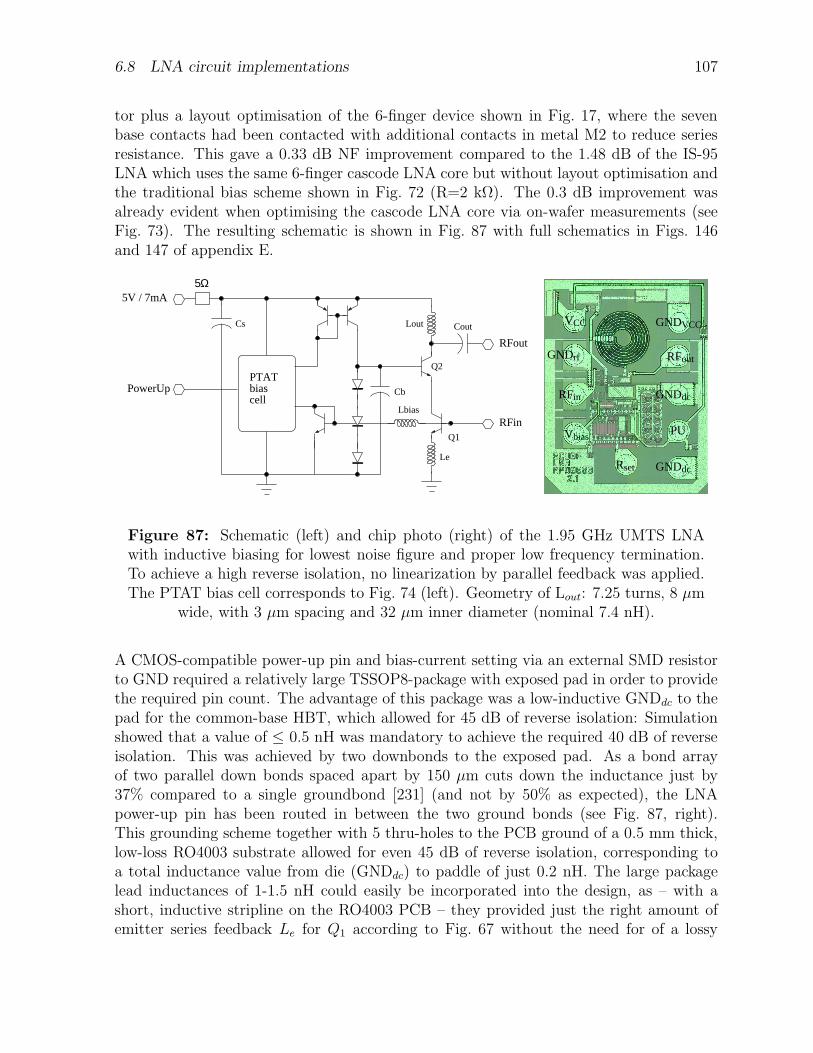
6.8 LNA circuit implementations 107
tor plus a layout optimisation of the 6-finger device shown in Fig. 17, where the sevenbase contacts had been contacted with additional contacts in metal M2 to reduce seriesresistance. This gave a 0.33 dB NF improvement compared to the 1.48 dB of the IS-95LNA which uses the same 6-finger cascode LNA core but without layout optimisation andthe traditional bias scheme shown in Fig. 72 (R=2 kΩ). The 0.3 dB improvement wasalready evident when optimising the cascode LNA core via on-wafer measurements (seeFig. 73). The resulting schematic is shown in Fig. 87 with full schematics in Figs. 146and 147 of appendix E.
cellbiasPTAT
Cs
Cb
Cout
RFin
Le
Q2
RFout
Lout
Q1
Lbias
PowerUp
5V / 7mA5Ω
VCC
GNDrf
RFin
Vbias
Rset GNDdc
GNDdc
RFout
GNDVCC
PU
Figure 87: Schematic (left) and chip photo (right) of the 1.95 GHz UMTS LNAwith inductive biasing for lowest noise figure and proper low frequency termination.To achieve a high reverse isolation, no linearization by parallel feedback was applied.The PTAT bias cell corresponds to Fig. 74 (left). Geometry of Lout: 7.25 turns, 8 µm
wide, with 3 µm spacing and 32 µm inner diameter (nominal 7.4 nH).
A CMOS-compatible power-up pin and bias-current setting via an external SMD resistorto GND required a relatively large TSSOP8-package with exposed pad in order to providethe required pin count. The advantage of this package was a low-inductive GNDdc to thepad for the common-base HBT, which allowed for 45 dB of reverse isolation: Simulationshowed that a value of ≤ 0.5 nH was mandatory to achieve the required 40 dB of reverseisolation. This was achieved by two downbonds to the exposed pad. As a bond arrayof two parallel down bonds spaced apart by 150 µm cuts down the inductance just by37% compared to a single groundbond [231] (and not by 50% as expected), the LNApower-up pin has been routed in between the two ground bonds (see Fig. 87, right).This grounding scheme together with 5 thru-holes to the PCB ground of a 0.5 mm thick,low-loss RO4003 substrate allowed for even 45 dB of reverse isolation, corresponding toa total inductance value from die (GNDdc) to paddle of just 0.2 nH. The large packagelead inductances of 1-1.5 nH could easily be incorporated into the design, as – with ashort, inductive stripline on the RO4003 PCB – they provided just the right amount ofemitter series feedback Le for Q1 according to Fig. 67 without the need for of a lossy
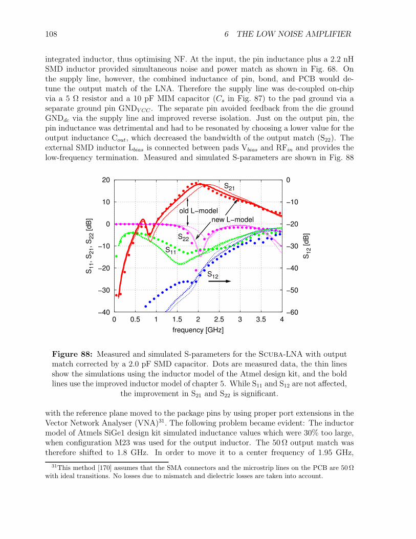
108 6 THE LOW NOISE AMPLIFIER
integrated inductor, thus optimising NF. At the input, the pin inductance plus a 2.2 nHSMD inductor provided simultaneous noise and power match as shown in Fig. 68. Onthe supply line, however, the combined inductance of pin, bond, and PCB would de-tune the output match of the LNA. Therefore the supply line was de-coupled on-chipvia a 5 Ω resistor and a 10 pF MIM capacitor (Cs in Fig. 87) to the pad ground via aseparate ground pin GNDV CC . The separate pin avoided feedback from the die groundGNDdc via the supply line and improved reverse isolation. Just on the output pin, thepin inductance was detrimental and had to be resonated by choosing a lower value for theoutput inductance Cout, which decreased the bandwidth of the output match (S22). Theexternal SMD inductor Lbias is connected between pads Vbias and RFin and provides thelow-frequency termination. Measured and simulated S-parameters are shown in Fig. 88
−40
−30
−20
−10
0
10
20
0 0.5 1 1.5 2 2.5 3 3.5 4−60
−50
−40
−30
−20
−10
0
S1
1, S
21, S
22 [dB
]
S1
2 [dB
]
frequency [GHz]
S21
S22
S11
S12
old L−model
new L−model
Figure 88: Measured and simulated S-parameters for the Scuba-LNA with outputmatch corrected by a 2.0 pF SMD capacitor. Dots are measured data, the thin linesshow the simulations using the inductor model of the Atmel design kit, and the boldlines use the improved inductor model of chapter 5. While S11 and S12 are not affected,
the improvement in S21 and S22 is significant.
with the reference plane moved to the package pins by using proper port extensions in theVector Network Analyser (VNA)31. The following problem became evident: The inductormodel of Atmels SiGe1 design kit simulated inductance values which were 30% too large,when configuration M23 was used for the output inductor. The 50 Ω output match wastherefore shifted to 1.8 GHz. In order to move it to a center frequency of 1.95 GHz,
31This method [170] assumes that the SMA connectors and the microstrip lines on the PCB are 50 Ωwith ideal transitions. No losses due to mismatch and dielectric losses are taken into account.
6.8 LNA circuit implementations 109
V2.1 w/o ESD Measurement ADS simulationICC@VCC = 5.0 V 6.75 mA 5.95 mA (incl. bandgap)
NFmin ≈ 0.9 dB 1.18 dBNF50,Ω 1.15 dB 1.52 dB
Rn 8.5 Ω 11.5 ΩΓopt 0.40 6 -77 0.40 6 -65
Table 18: Simulated and measured noise parameters of the Scuba LNA. Lower NFand Rn is due to a higher current gain and lower base resistance compared to the
design kit
an external SMD capacitor of 2 pF was necessary in series to the integrated 0.55 pFMIM, leading to an effective value for the output capacitor of 0.43 pF. Improved inductormodels were developed as described in section 5. Resimulating the circuit using thisimproved model, together with the 2 pF SMD capacitor, shows superior agreement withthe measurement. The remaining differences are due to an insufficient package equivalentcircuit. The notch in the transfer characteristics at 800 MHz is due to a resonancein the supply line between the integrated 10 pF blocking capacitors, the bondwire andpackage inductance and the 100 pF SMD capacitor on the PCB. It would be even moresevere if not damped by the 5 Ω resistor in the supply line (see Fig, 87, left). Using alarger value, e.g. 12 Ω in the case of the WLAN LNAs (Fig. 150), the notch is hardlyvisible. As explained in [192], care needs to be taken when applying on-chip decoupling tocomplicated transceiver designs, as – at frequencies close to resonance – isolation betweenadjacent blocks is reduced. The simulated and measured noise parameters are comparedin table 18. Integrating the input blocking capacitor on-chip would increase the excellentNF of 1.15 dB by 0.5 dB.
OIP3 has been evaluated for 2 boards with different emitter series feedback inductanceand a supply voltage of 3 and 5 V. As the common-base device is biased at a basevoltage of 3 × VBE , at a supply voltage of 3 V the LNA is limited in output swing andthe linearity is considerably lower compared to 5 V. The bias inductor terminates thebeat frequency down to ”0” frequency. Therefore OIP3 versus tone spacing in Fig. 89is extremely flat down to very low tone spacings in the two-tone linearity measurement.Due to the low-impedance termination at low frequencies, the difference between the twoside-bands (USB, LSB) is low. The dip in OIP3 around 10 MHz is due to a parallelresonance of the 47 nH bias inductor with the 10 nF blocking capacitor towards the 50 Ωsource, which forms a high impedance to the beat frequency. In Fig. 90 the current ofthe UMTS LNA has been swept by decreasing the value of the SMD resistor that sets thebandgap current. While the optimum NF for the used transistor size is reached at lowcurrents, gain improves with current due to gm = IC/Vth. OIP3 dips at 12 mA, as abovethat frequency the maximum current of the 2-finger cascode HBT is exceeded.
In Fig. 91 inductive and resistive biasing is compared experimentally (ICC = 6.6 mA,f = 1950 MHz, tone spacing = 5 MHz). Optimum performance is achieved with a bias
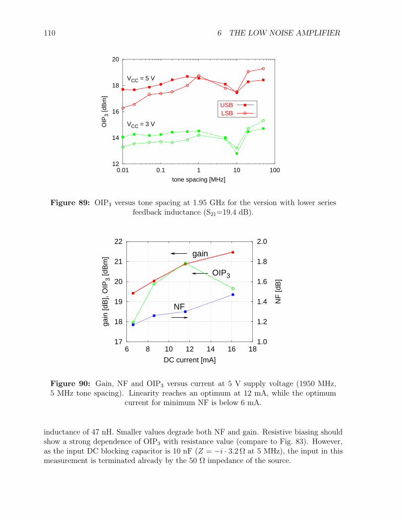
110 6 THE LOW NOISE AMPLIFIER
12
14
16
18
20
0.01 0.1 1 10 100
OIP
3 [d
Bm
]
tone spacing [MHz]
VCC = 5 V
VCC = 3 V
USBLSB
Figure 89: OIP3 versus tone spacing at 1.95 GHz for the version with lower seriesfeedback inductance (S21=19.4 dB).
17
18
19
20
21
22
6 8 10 12 14 16 181.0
1.2
1.4
1.6
1.8
2.0
gain
[dB
], O
IP3
[dB
m]
NF
[dB
]
DC current [mA]
gain
OIP3
NF
Figure 90: Gain, NF and OIP3 versus current at 5 V supply voltage (1950 MHz,5 MHz tone spacing). Linearity reaches an optimum at 12 mA, while the optimum
current for minimum NF is below 6 mA.
inductance of 47 nH. Smaller values degrade both NF and gain. Resistive biasing shouldshow a strong dependence of OIP3 with resistance value (compare to Fig. 83). However,as the input DC blocking capacitor is 10 nF (Z = −i · 3.2 Ω at 5 MHz), the input in thismeasurement is terminated already by the 50 Ω impedance of the source.
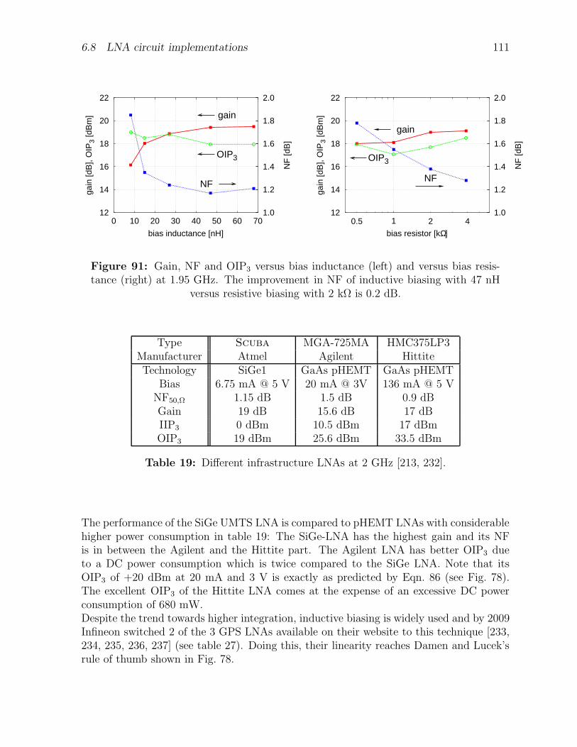
6.8 LNA circuit implementations 111
12
14
16
18
20
22
0 10 20 30 40 50 60 701.0
1.2
1.4
1.6
1.8
2.0ga
in [d
B],
OIP
3 [d
Bm
]
NF
[dB
]
bias inductance [nH]
gain
OIP3
NF
12
14
16
18
20
22
11.0
1.2
1.4
1.6
1.8
2.0
gain
[dB
], O
IP3
[dB
m]
NF
[dB
]
bias resistor [kΩ]
gain
OIP3
NF
0.5 2 4
Figure 91: Gain, NF and OIP3 versus bias inductance (left) and versus bias resis-tance (right) at 1.95 GHz. The improvement in NF of inductive biasing with 47 nH
versus resistive biasing with 2 kΩ is 0.2 dB.
Type Scuba MGA-725MA HMC375LP3Manufacturer Atmel Agilent HittiteTechnology SiGe1 GaAs pHEMT GaAs pHEMT
Bias 6.75 mA @ 5 V 20 mA @ 3V 136 mA @ 5 VNF50,Ω 1.15 dB 1.5 dB 0.9 dBGain 19 dB 15.6 dB 17 dBIIP3 0 dBm 10.5 dBm 17 dBmOIP3 19 dBm 25.6 dBm 33.5 dBm
Table 19: Different infrastructure LNAs at 2 GHz [213, 232].
The performance of the SiGe UMTS LNA is compared to pHEMT LNAs with considerablehigher power consumption in table 19: The SiGe-LNA has the highest gain and its NFis in between the Agilent and the Hittite part. The Agilent LNA has better OIP3 dueto a DC power consumption which is twice compared to the SiGe LNA. Note that itsOIP3 of +20 dBm at 20 mA and 3 V is exactly as predicted by Eqn. 86 (see Fig. 78).The excellent OIP3 of the Hittite LNA comes at the expense of an excessive DC powerconsumption of 680 mW.Despite the trend towards higher integration, inductive biasing is widely used and by 2009Infineon switched 2 of the 3 GPS LNAs available on their website to this technique [233,234, 235, 236, 237] (see table 27). Doing this, their linearity reaches Damen and Lucek’srule of thumb shown in Fig. 78.
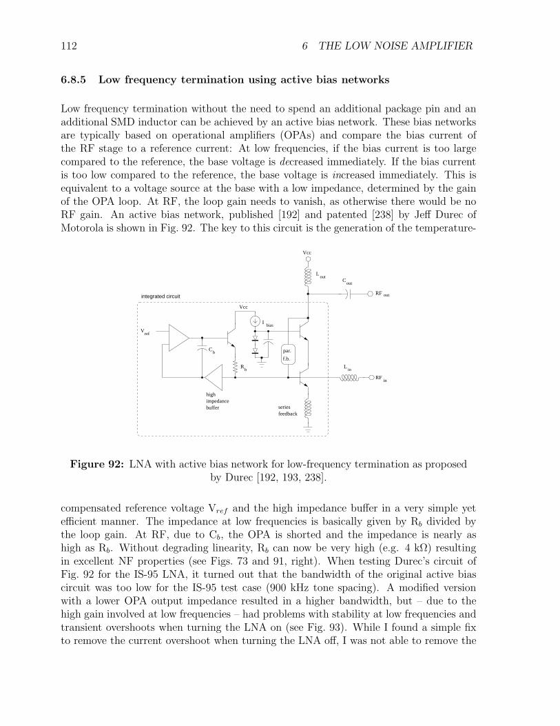
112 6 THE LOW NOISE AMPLIFIER
6.8.5 Low frequency termination using active bias networks
Low frequency termination without the need to spend an additional package pin and anadditional SMD inductor can be achieved by an active bias network. These bias networksare typically based on operational amplifiers (OPAs) and compare the bias current ofthe RF stage to a reference current: At low frequencies, if the bias current is too largecompared to the reference, the base voltage is decreased immediately. If the bias currentis too low compared to the reference, the base voltage is increased immediately. This isequivalent to a voltage source at the base with a low impedance, determined by the gainof the OPA loop. At RF, the loop gain needs to vanish, as otherwise there would be noRF gain. An active bias network, published [192] and patented [238] by Jeff Durec ofMotorola is shown in Fig. 92. The key to this circuit is the generation of the temperature-
Lout
Ibias
Rb
Cb
Vref
Cout
RF
seriesfeedback
Lin
Vcc
highimpedancebuffer
RFin
f.b.
par.
out
Vcc
integrated circuit
Figure 92: LNA with active bias network for low-frequency termination as proposedby Durec [192, 193, 238].
compensated reference voltage Vref and the high impedance buffer in a very simple yetefficient manner. The impedance at low frequencies is basically given by Rb divided bythe loop gain. At RF, due to Cb, the OPA is shorted and the impedance is nearly ashigh as Rb. Without degrading linearity, Rb can now be very high (e.g. 4 kΩ) resultingin excellent NF properties (see Figs. 73 and 91, right). When testing Durec’s circuit ofFig. 92 for the IS-95 LNA, it turned out that the bandwidth of the original active biascircuit was too low for the IS-95 test case (900 kHz tone spacing). A modified versionwith a lower OPA output impedance resulted in a higher bandwidth, but – due to thehigh gain involved at low frequencies – had problems with stability at low frequencies andtransient overshoots when turning the LNA on (see Fig. 93). While I found a simple fixto remove the current overshoot when turning the LNA off, I was not able to remove the
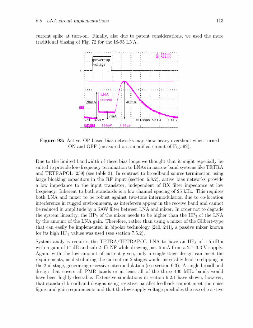
6.8 LNA circuit implementations 113
current spike at turn-on. Finally, also due to patent considerations, we used the moretraditional biasing of Fig. 72 for the IS-95 LNA.
7mA
40mA
voltagepower−up
28mA
LNAcurrent
Figure 93: Active, OP-based bias networks may show heavy overshoot when turnedON and OFF (measured on a modified circuit of Fig. 92).
Due to the limited bandwidth of these bias loops we thought that it might especially besuited to provide low-frequency termination to LNAs in narrow band systems like TETRAand TETRAPOL [239] (see table 3). In contrast to broadband source termination usinglarge blocking capacitors in the RF input (section 6.8.2), active bias networks providea low impedance to the input transistor, independent of RX filter impedance at lowfrequency. Inherent to both standards is a low channel spacing of 25 kHz. This requiresboth LNA and mixer to be robust against two-tone intermodulation due to co-locationinterference in rugged environments, as interferers appear in the receive band and cannotbe reduced in amplitude by a SAW filter between LNA and mixer. In order not to degradethe system linearity, the IIP3 of the mixer needs to be higher than the IIP3 of the LNAby the amount of the LNA gain. Therefore, rather than using a mixer of the Gilbert-typethat can easily be implemented in bipolar technology [240, 241], a passive mixer knownfor its high IIP3 values was used (see section 7.5.2).
System analysis requires the TETRA/TETRAPOL LNA to have an IIP3 of +5 dBmwith a gain of 17 dB and sub 2 dB NF while drawing just 6 mA from a 2.7–3.3 V supply.Again, with the low amount of current given, only a single-stage design can meet therequirements, as distributing the current on 2 stages would inevitably lead to clipping inthe 2nd stage, generating excessive intermodulation (see section 6.3). A single broadbanddesign that covers all PMR bands or at least all of the three 400 MHz bands wouldhave been highly desirable. Extensive simulations in section 6.2.1 have shown, however,that standard broadband designs using resistive parallel feedback cannot meet the noisefigure and gain requirements and that the low supply voltage precludes the use of resistive
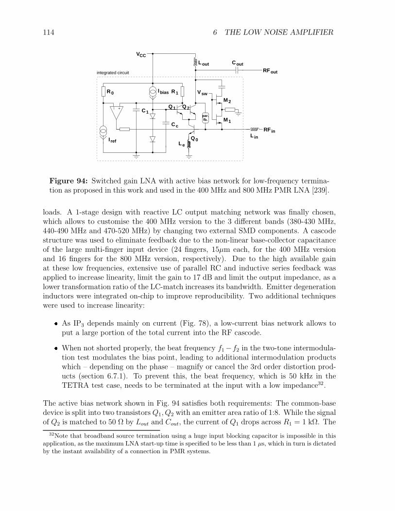
114 6 THE LOW NOISE AMPLIFIER
VCC
Cout
L erefI
Ibias
outRF
RF in
outL
L in
M2
M1
Q0
R1
C1
Cc
R0
Q1 Q2
Vsw
fb.par.
integrated circuit
Figure 94: Switched gain LNA with active bias network for low-frequency termina-tion as proposed in this work and used in the 400 MHz and 800 MHz PMR LNA [239].
loads. A 1-stage design with reactive LC output matching network was finally chosen,which allows to customise the 400 MHz version to the 3 different bands (380-430 MHz,440-490 MHz and 470-520 MHz) by changing two external SMD components. A cascodestructure was used to eliminate feedback due to the non-linear base-collector capacitanceof the large multi-finger input device (24 fingers, 15µm each, for the 400 MHz versionand 16 fingers for the 800 MHz version, respectively). Due to the high available gainat these low frequencies, extensive use of parallel RC and inductive series feedback wasapplied to increase linearity, limit the gain to 17 dB and limit the output impedance, as alower transformation ratio of the LC-match increases its bandwidth. Emitter degenerationinductors were integrated on-chip to improve reproducibility. Two additional techniqueswere used to increase linearity: As IP3 depends mainly on current (Fig. 78), a low-current bias network allows to
put a large portion of the total current into the RF cascode. When not shorted properly, the beat frequency f1−f2 in the two-tone intermodula-tion test modulates the bias point, leading to additional intermodulation productswhich – depending on the phase – magnify or cancel the 3rd order distortion prod-ucts (section 6.7.1). To prevent this, the beat frequency, which is 50 kHz in theTETRA test case, needs to be terminated at the input with a low impedance32.
The active bias network shown in Fig. 94 satisfies both requirements: The common-basedevice is split into two transistors Q1, Q2 with an emitter area ratio of 1:8. While the signalof Q2 is matched to 50 Ω by Lout and Cout, the current of Q1 drops across R1 = 1 kΩ. The
32Note that broadband source termination using a huge input blocking capacitor is impossible in thisapplication, as the maximum LNA start-up time is specified to be less than 1 µs, which in turn is dictatedby the instant availability of a connection in PMR systems.
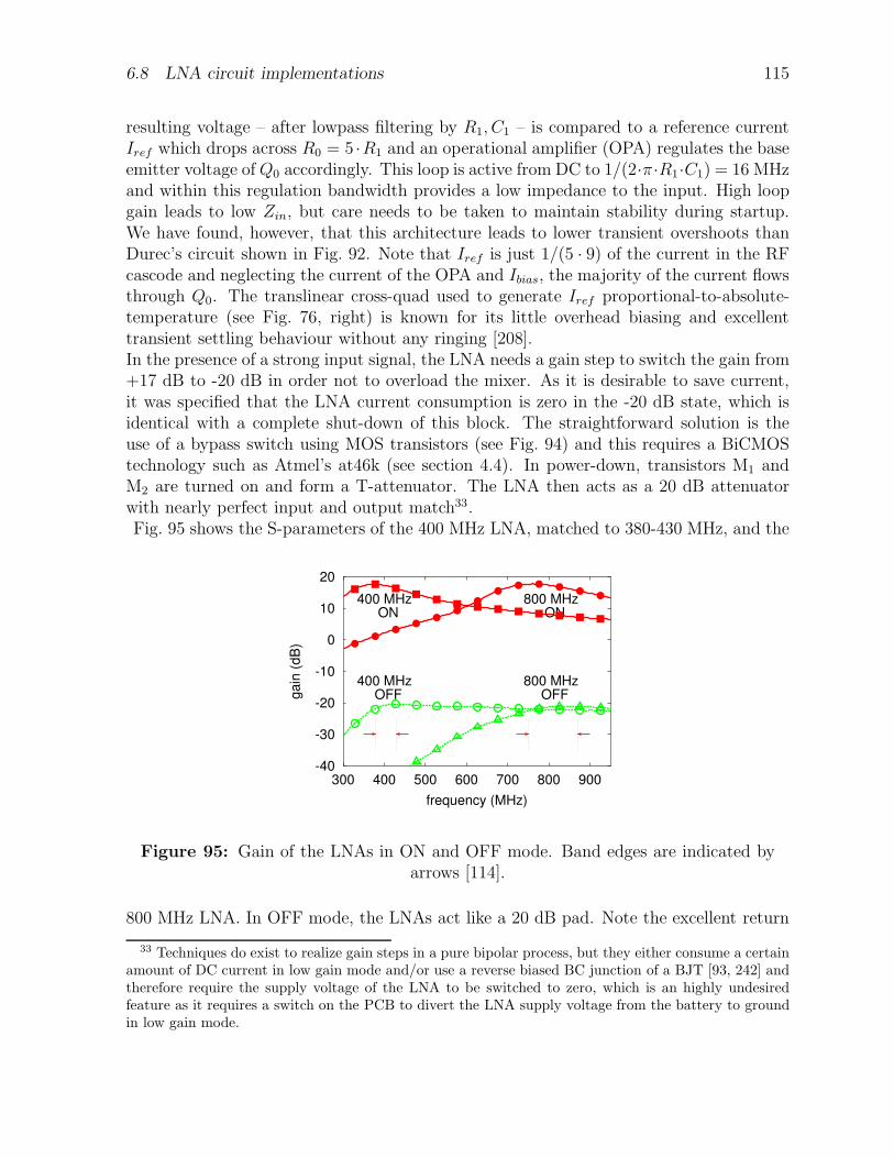
6.8 LNA circuit implementations 115
resulting voltage – after lowpass filtering by R1, C1 – is compared to a reference currentIref which drops across R0 = 5 ·R1 and an operational amplifier (OPA) regulates the baseemitter voltage of Q0 accordingly. This loop is active from DC to 1/(2·π·R1·C1) = 16 MHzand within this regulation bandwidth provides a low impedance to the input. High loopgain leads to low Zin, but care needs to be taken to maintain stability during startup.We have found, however, that this architecture leads to lower transient overshoots thanDurec’s circuit shown in Fig. 92. Note that Iref is just 1/(5 · 9) of the current in the RFcascode and neglecting the current of the OPA and Ibias, the majority of the current flowsthrough Q0. The translinear cross-quad used to generate Iref proportional-to-absolute-temperature (see Fig. 76, right) is known for its little overhead biasing and excellenttransient settling behaviour without any ringing [208].In the presence of a strong input signal, the LNA needs a gain step to switch the gain from+17 dB to -20 dB in order not to overload the mixer. As it is desirable to save current,it was specified that the LNA current consumption is zero in the -20 dB state, which isidentical with a complete shut-down of this block. The straightforward solution is theuse of a bypass switch using MOS transistors (see Fig. 94) and this requires a BiCMOStechnology such as Atmel’s at46k (see section 4.4). In power-down, transistors M1 andM2 are turned on and form a T-attenuator. The LNA then acts as a 20 dB attenuatorwith nearly perfect input and output match33.Fig. 95 shows the S-parameters of the 400 MHz LNA, matched to 380-430 MHz, and the
-40
-30
-20
-10
0
10
20
300 400 500 600 700 800 900
gain
(dB
)
frequency (MHz)
400 MHz ON
400 MHz OFF
800 MHz ON
800 MHz OFF
Figure 95: Gain of the LNAs in ON and OFF mode. Band edges are indicated byarrows [114].
800 MHz LNA. In OFF mode, the LNAs act like a 20 dB pad. Note the excellent return
33 Techniques do exist to realize gain steps in a pure bipolar process, but they either consume a certainamount of DC current in low gain mode and/or use a reverse biased BC junction of a BJT [93, 242] andtherefore require the supply voltage of the LNA to be switched to zero, which is an highly undesiredfeature as it requires a switch on the PCB to divert the LNA supply voltage from the battery to groundin low gain mode.
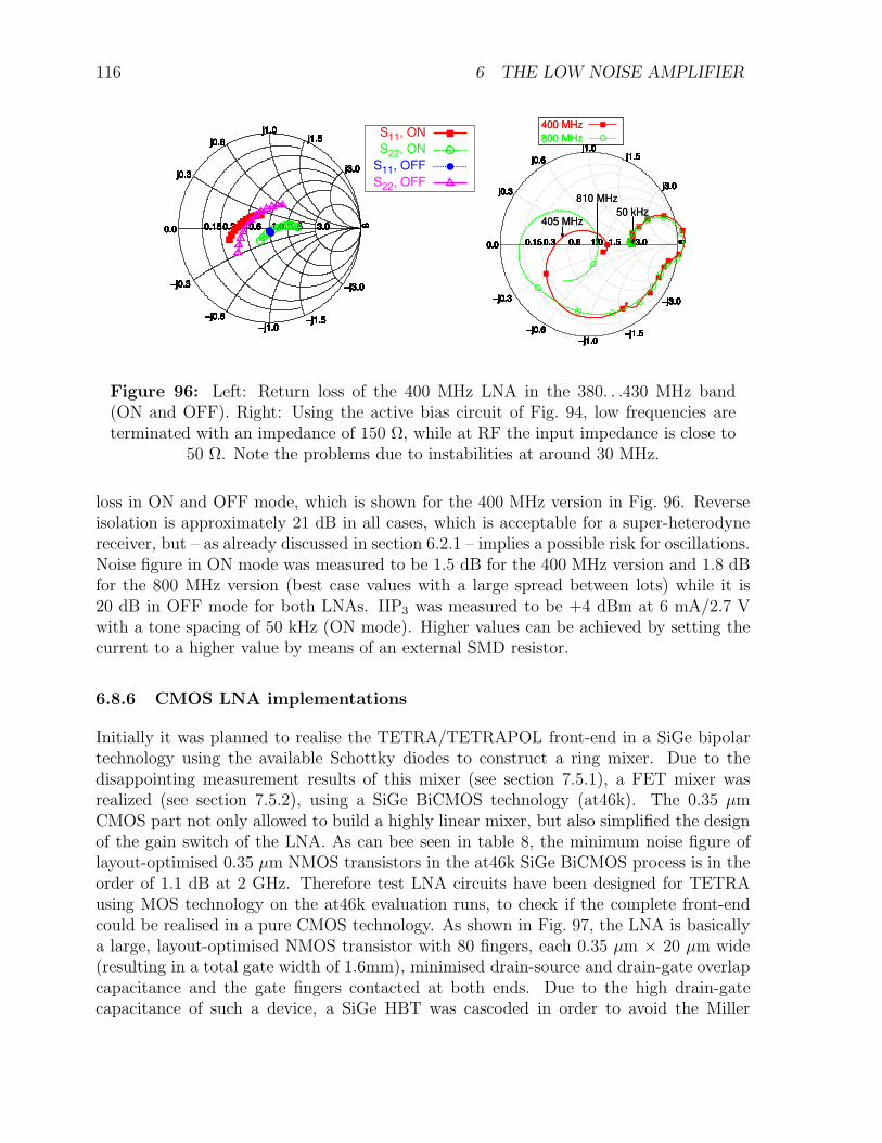
116 6 THE LOW NOISE AMPLIFIER
j0.3
j0.6
j1.0j1.5
j3.0
−j0.3
−j0.6
−j1.0−j1.5
−j3.0
0.150.3 0.6 1.0 1.5 3.00.0 8
j0.3
j0.6
j1.0j1.5
j3.0
−j0.3
−j0.6
−j1.0−j1.5
−j3.0
0.150.3 0.6 1.0 1.5 3.00.0 8
j0.3
j0.6
j1.0j1.5
j3.0
−j0.3
−j0.6
−j1.0−j1.5
−j3.0
0.150.3 0.6 1.0 1.5 3.00.0 8
j0.3
j0.6
j1.0j1.5
j3.0
−j0.3
−j0.6
−j1.0−j1.5
−j3.0
0.150.3 0.6 1.0 1.5 3.00.0 8
j0.3
j0.6
j1.0j1.5
j3.0
−j0.3
−j0.6
−j1.0−j1.5
−j3.0
0.150.3 0.6 1.0 1.5 3.00.0 8
j0.3
j0.6
j1.0j1.5
j3.0
−j0.3
−j0.6
−j1.0−j1.5
−j3.0
0.150.3 0.6 1.0 1.5 3.00.0 8
j0.3
j0.6
j1.0j1.5
j3.0
−j0.3
−j0.6
−j1.0−j1.5
−j3.0
0.150.3 0.6 1.0 1.5 3.00.0 8
j0.3
j0.6
j1.0j1.5
j3.0
−j0.3
−j0.6
−j1.0−j1.5
−j3.0
0.150.3 0.6 1.0 1.5 3.00.0 8
j0.3
j0.6
j1.0j1.5
j3.0
−j0.3
−j0.6
−j1.0−j1.5
−j3.0
0.150.3 0.6 1.0 1.5 3.00.0 8
j0.3
j0.6
j1.0j1.5
j3.0
−j0.3
−j0.6
−j1.0−j1.5
−j3.0
0.150.3 0.6 1.0 1.5 3.00.0 8
j0.3
j0.6
j1.0j1.5
j3.0
−j0.3
−j0.6
−j1.0−j1.5
−j3.0
0.150.3 0.6 1.0 1.5 3.00.0 8
j0.3
j0.6
j1.0j1.5
j3.0
−j0.3
−j0.6
−j1.0−j1.5
−j3.0
0.150.3 0.6 1.0 1.5 3.00.0 8
j0.3
j0.6
j1.0j1.5
j3.0
−j0.3
−j0.6
−j1.0−j1.5
−j3.0
0.150.3 0.6 1.0 1.5 3.00.0 8
j0.3
j0.6
j1.0j1.5
j3.0
−j0.3
−j0.6
−j1.0−j1.5
−j3.0
0.150.3 0.6 1.0 1.5 3.00.0 8
j0.3
j0.6
j1.0j1.5
j3.0
−j0.3
−j0.6
−j1.0−j1.5
−j3.0
0.150.3 0.6 1.0 1.5 3.00.0 8
j0.3
j0.6
j1.0j1.5
j3.0
−j0.3
−j0.6
−j1.0−j1.5
−j3.0
0.150.3 0.6 1.0 1.5 3.00.0 8
j0.3
j0.6
j1.0j1.5
j3.0
−j0.3
−j0.6
−j1.0−j1.5
−j3.0
0.150.3 0.6 1.0 1.5 3.00.0 8
j0.3
j0.6
j1.0j1.5
j3.0
−j0.3
−j0.6
−j1.0−j1.5
−j3.0
0.150.3 0.6 1.0 1.5 3.00.0 8
j0.3
j0.6
j1.0j1.5
j3.0
−j0.3
−j0.6
−j1.0−j1.5
−j3.0
0.150.3 0.6 1.0 1.5 3.00.0 8
S11, ON
S22, ON
S11, OFF
S22, OFFj0.3
j0.6
j1.0j1.5
j3.0
−j0.3
−j0.6
−j1.0−j1.5
−j3.0
0.15 0.3 0.6 1.0 1.5 3.00.0 8
j0.3
j0.6
j1.0j1.5
j3.0
−j0.3
−j0.6
−j1.0−j1.5
−j3.0
0.15 0.3 0.6 1.0 1.5 3.00.0 8
j0.3
j0.6
j1.0j1.5
j3.0
−j0.3
−j0.6
−j1.0−j1.5
−j3.0
0.15 0.3 0.6 1.0 1.5 3.00.0 8
j0.3
j0.6
j1.0j1.5
j3.0
−j0.3
−j0.6
−j1.0−j1.5
−j3.0
0.15 0.3 0.6 1.0 1.5 3.00.0 8
j0.3
j0.6
j1.0j1.5
j3.0
−j0.3
−j0.6
−j1.0−j1.5
−j3.0
0.15 0.3 0.6 1.0 1.5 3.00.0 8
j0.3
j0.6
j1.0j1.5
j3.0
−j0.3
−j0.6
−j1.0−j1.5
−j3.0
0.15 0.3 0.6 1.0 1.5 3.00.0 8
j0.3
j0.6
j1.0j1.5
j3.0
−j0.3
−j0.6
−j1.0−j1.5
−j3.0
0.15 0.3 0.6 1.0 1.5 3.00.0 8
j0.3
j0.6
j1.0j1.5
j3.0
−j0.3
−j0.6
−j1.0−j1.5
−j3.0
0.15 0.3 0.6 1.0 1.5 3.00.0 8
j0.3
j0.6
j1.0j1.5
j3.0
−j0.3
−j0.6
−j1.0−j1.5
−j3.0
0.15 0.3 0.6 1.0 1.5 3.00.0 8
j0.3
j0.6
j1.0j1.5
j3.0
−j0.3
−j0.6
−j1.0−j1.5
−j3.0
0.15 0.3 0.6 1.0 1.5 3.00.0 8
j0.3
j0.6
j1.0j1.5
j3.0
−j0.3
−j0.6
−j1.0−j1.5
−j3.0
0.15 0.3 0.6 1.0 1.5 3.00.0 8
j0.3
j0.6
j1.0j1.5
j3.0
−j0.3
−j0.6
−j1.0−j1.5
−j3.0
0.15 0.3 0.6 1.0 1.5 3.00.0 8
j0.3
j0.6
j1.0j1.5
j3.0
−j0.3
−j0.6
−j1.0−j1.5
−j3.0
0.15 0.3 0.6 1.0 1.5 3.00.0 8
j0.3
j0.6
j1.0j1.5
j3.0
−j0.3
−j0.6
−j1.0−j1.5
−j3.0
0.15 0.3 0.6 1.0 1.5 3.00.0 8
j0.3
j0.6
j1.0j1.5
j3.0
−j0.3
−j0.6
−j1.0−j1.5
−j3.0
0.15 0.3 0.6 1.0 1.5 3.00.0 8
j0.3
j0.6
j1.0j1.5
j3.0
−j0.3
−j0.6
−j1.0−j1.5
−j3.0
0.15 0.3 0.6 1.0 1.5 3.00.0 8
j0.3
j0.6
j1.0j1.5
j3.0
−j0.3
−j0.6
−j1.0−j1.5
−j3.0
0.15 0.3 0.6 1.0 1.5 3.00.0 8
j0.3
j0.6
j1.0j1.5
j3.0
−j0.3
−j0.6
−j1.0−j1.5
−j3.0
0.15 0.3 0.6 1.0 1.5 3.00.0 8
j0.3
j0.6
j1.0j1.5
j3.0
−j0.3
−j0.6
−j1.0−j1.5
−j3.0
0.15 0.3 0.6 1.0 1.5 3.00.0 8
50 kHz405 MHz
810 MHz
400 MHz
800 MHz
j0.3
j0.6
j1.0j1.5
j3.0
−j0.3
−j0.6
−j1.0−j1.5
−j3.0
0.15 0.3 0.6 1.0 1.5 3.00.0 8
50 kHz405 MHz
810 MHz
400 MHz
800 MHz
Figure 96: Left: Return loss of the 400 MHz LNA in the 380. . .430 MHz band(ON and OFF). Right: Using the active bias circuit of Fig. 94, low frequencies areterminated with an impedance of 150 Ω, while at RF the input impedance is close to
50 Ω. Note the problems due to instabilities at around 30 MHz.
loss in ON and OFF mode, which is shown for the 400 MHz version in Fig. 96. Reverseisolation is approximately 21 dB in all cases, which is acceptable for a super-heterodynereceiver, but – as already discussed in section 6.2.1 – implies a possible risk for oscillations.Noise figure in ON mode was measured to be 1.5 dB for the 400 MHz version and 1.8 dBfor the 800 MHz version (best case values with a large spread between lots) while it is20 dB in OFF mode for both LNAs. IIP3 was measured to be +4 dBm at 6 mA/2.7 Vwith a tone spacing of 50 kHz (ON mode). Higher values can be achieved by setting thecurrent to a higher value by means of an external SMD resistor.
6.8.6 CMOS LNA implementations
Initially it was planned to realise the TETRA/TETRAPOL front-end in a SiGe bipolartechnology using the available Schottky diodes to construct a ring mixer. Due to thedisappointing measurement results of this mixer (see section 7.5.1), a FET mixer wasrealized (see section 7.5.2), using a SiGe BiCMOS technology (at46k). The 0.35 µmCMOS part not only allowed to build a highly linear mixer, but also simplified the designof the gain switch of the LNA. As can bee seen in table 8, the minimum noise figure oflayout-optimised 0.35 µm NMOS transistors in the at46k SiGe BiCMOS process is in theorder of 1.1 dB at 2 GHz. Therefore test LNA circuits have been designed for TETRAusing MOS technology on the at46k evaluation runs, to check if the complete front-endcould be realised in a pure CMOS technology. As shown in Fig. 97, the LNA is basicallya large, layout-optimised NMOS transistor with 80 fingers, each 0.35 µm × 20 µm wide(resulting in a total gate width of 1.6mm), minimised drain-source and drain-gate overlapcapacitance and the gate fingers contacted at both ends. Due to the high drain-gatecapacitance of such a device, a SiGe HBT was cascoded in order to avoid the Miller
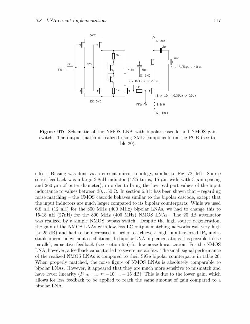
6.8 LNA circuit implementations 117
Figure 97: Schematic of the NMOS LNA with bipolar cascode and NMOS gainswitch. The output match is realized using SMD components on the PCB (see ta-
ble 20).
effect. Biasing was done via a current mirror topology, similar to Fig. 72, left. Sourceseries feedback was a large 3.8nH inductor (4.25 turns, 15 µm wide with 3 µm spacingand 260 µm of outer diameter), in order to bring the low real part values of the inputinductance to values between 30. . .50 Ω. In section 6.3 it has been shown that – regardingnoise matching – the CMOS cascode behaves similar to the bipolar cascode, except thatthe input inductors are much larger compared to its bipolar counterparts: While we used6.8 nH (12 nH) for the 800 MHz (400 MHz) bipolar LNAs, we had to change this to15-18 nH (27nH) for the 800 MHz (400 MHz) NMOS LNAs. The 20 dB attenuatorwas realized by a simple NMOS bypass switch. Despite the high source degeneration,the gain of the NMOS LNAs with low-loss LC output matching networks was very high(> 25 dB) and had to be decreased in order to achieve a high input-referred IP3 and astable operation without oscillations. In bipolar LNA implementations it is possible to useparallel, capacitive feedback (see section 6.6) for low-noise linearization. For the NMOSLNA, however, a feedback capacitor led to severe instability. The small signal performanceof the realized NMOS LNAs is compared to their SiGe bipolar counterparts in table 20.When properly matched, the noise figure of NMOS LNAs is absolutely comparable tobipolar LNAs. However, it appeared that they are much more sensitive to mismatch andhave lower linearity (P1dB,input ≈ −10 . . . − 15 dB). This is due to the lower gain, whichallows for less feedback to be applied to reach the same amount of gain compared to abipolar LNA.
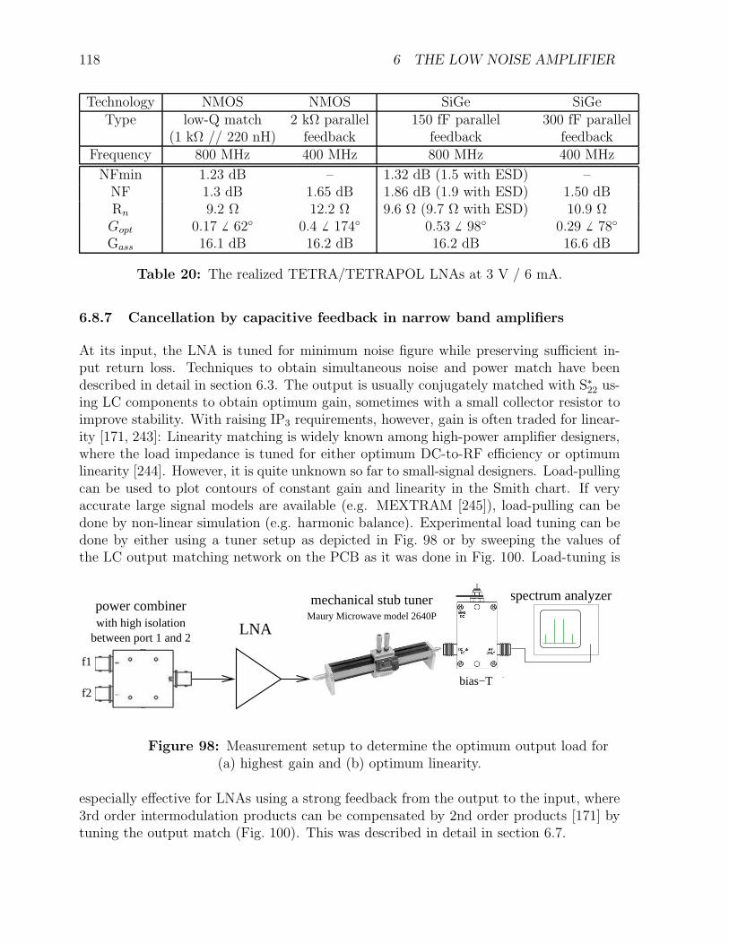
118 6 THE LOW NOISE AMPLIFIER
Technology NMOS NMOS SiGe SiGeType low-Q match 2 kΩ parallel 150 fF parallel 300 fF parallel
(1 kΩ // 220 nH) feedback feedback feedbackFrequency 800 MHz 400 MHz 800 MHz 400 MHz
NFmin 1.23 dB – 1.32 dB (1.5 with ESD) –NF 1.3 dB 1.65 dB 1.86 dB (1.9 with ESD) 1.50 dBRn 9.2 Ω 12.2 Ω 9.6 Ω (9.7 Ω with ESD) 10.9 ΩGopt 0.17 6 62 0.4 6 174 0.53 6 98 0.29 6 78
Gass 16.1 dB 16.2 dB 16.2 dB 16.6 dB
Table 20: The realized TETRA/TETRAPOL LNAs at 3 V / 6 mA.
6.8.7 Cancellation by capacitive feedback in narrow band amplifiers
At its input, the LNA is tuned for minimum noise figure while preserving sufficient in-put return loss. Techniques to obtain simultaneous noise and power match have beendescribed in detail in section 6.3. The output is usually conjugately matched with S∗
22 us-ing LC components to obtain optimum gain, sometimes with a small collector resistor toimprove stability. With raising IP3 requirements, however, gain is often traded for linear-ity [171, 243]: Linearity matching is widely known among high-power amplifier designers,where the load impedance is tuned for either optimum DC-to-RF efficiency or optimumlinearity [244]. However, it is quite unknown so far to small-signal designers. Load-pullingcan be used to plot contours of constant gain and linearity in the Smith chart. If veryaccurate large signal models are available (e.g. MEXTRAM [245]), load-pulling can bedone by non-linear simulation (e.g. harmonic balance). Experimental load tuning can bedone by either using a tuner setup as depicted in Fig. 98 or by sweeping the values ofthe LC output matching network on the PCB as it was done in Fig. 100. Load-tuning is
LNA
f1
f2
spectrum analyzer
bias−T
mechanical stub tunerMaury Microwave model 2640P
between port 1 and 2
power combinerwith high isolation
Figure 98: Measurement setup to determine the optimum output load for(a) highest gain and (b) optimum linearity.
especially effective for LNAs using a strong feedback from the output to the input, where3rd order intermodulation products can be compensated by 2nd order products [171] bytuning the output match (Fig. 100). This was described in detail in section 6.7.
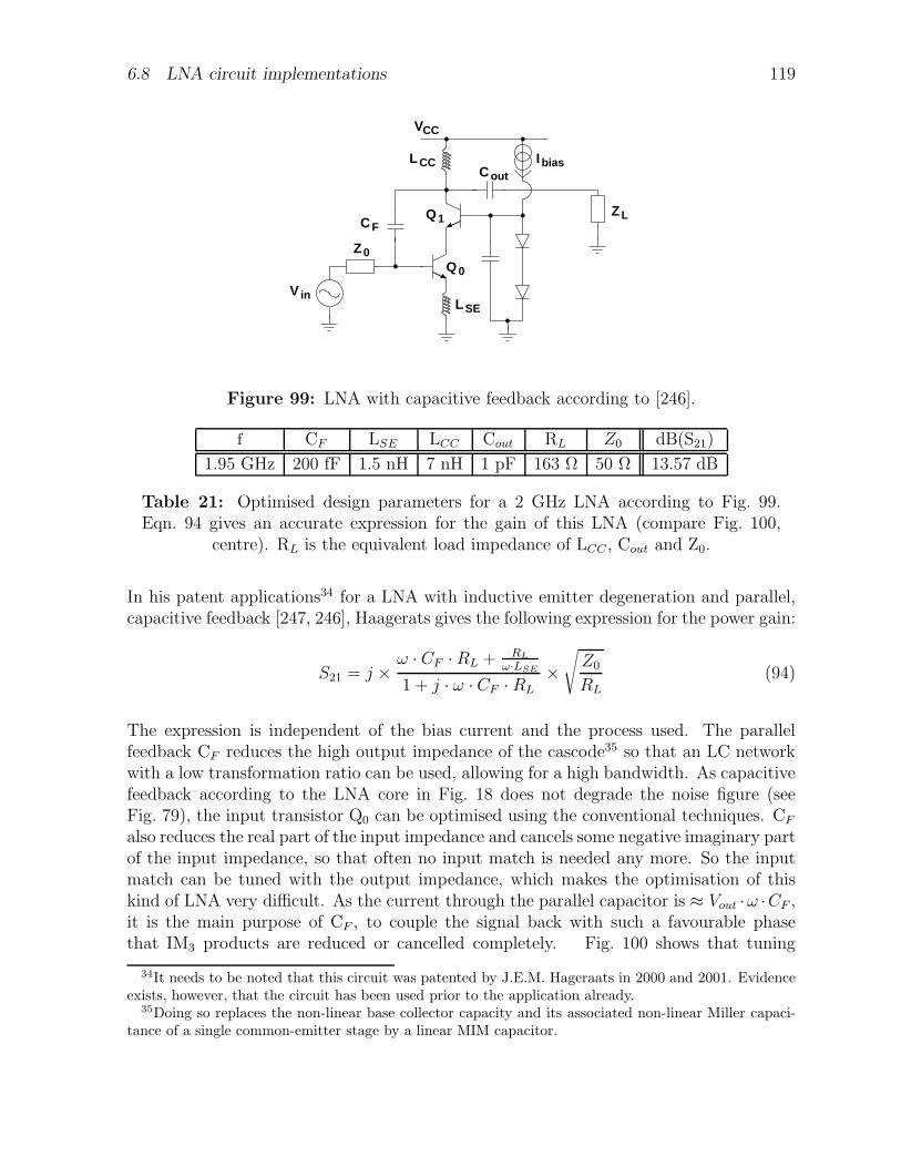
6.8 LNA circuit implementations 119
VCC
CF
outC
Z0
Ibias
V in
LZ
Q0
L SE
L CC
Q1
Figure 99: LNA with capacitive feedback according to [246].
f CF LSE LCC Cout RL Z0 dB(S21)
1.95 GHz 200 fF 1.5 nH 7 nH 1 pF 163 Ω 50 Ω 13.57 dB
Table 21: Optimised design parameters for a 2 GHz LNA according to Fig. 99.Eqn. 94 gives an accurate expression for the gain of this LNA (compare Fig. 100,
centre). RL is the equivalent load impedance of LCC , Cout and Z0.
In his patent applications34 for a LNA with inductive emitter degeneration and parallel,capacitive feedback [247, 246], Haagerats gives the following expression for the power gain:
S21 = j ×ω · CF · RL + RL
ω·LSE
1 + j · ω · CF · RL×√
Z0
RL(94)
The expression is independent of the bias current and the process used. The parallelfeedback CF reduces the high output impedance of the cascode35 so that an LC networkwith a low transformation ratio can be used, allowing for a high bandwidth. As capacitivefeedback according to the LNA core in Fig. 18 does not degrade the noise figure (seeFig. 79), the input transistor Q0 can be optimised using the conventional techniques. CF
also reduces the real part of the input impedance and cancels some negative imaginary partof the input impedance, so that often no input match is needed any more. So the inputmatch can be tuned with the output impedance, which makes the optimisation of thiskind of LNA very difficult. As the current through the parallel capacitor is ≈ Vout ·ω ·CF ,it is the main purpose of CF , to couple the signal back with such a favourable phasethat IM3 products are reduced or cancelled completely. Fig. 100 shows that tuning
34It needs to be noted that this circuit was patented by J.E.M. Hageraats in 2000 and 2001. Evidenceexists, however, that the circuit has been used prior to the application already.
35Doing so replaces the non-linear base collector capacity and its associated non-linear Miller capaci-tance of a single common-emitter stage by a linear MIM capacitor.
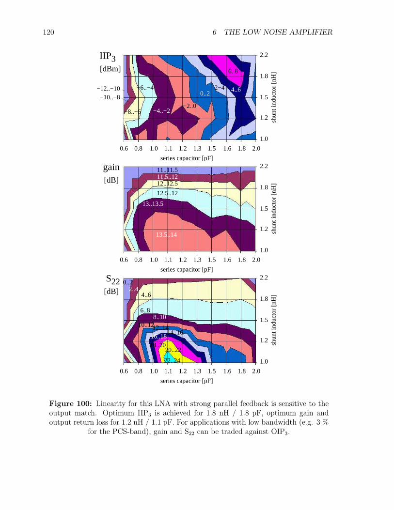
120 6 THE LOW NOISE AMPLIFIER
series capacitor [pF]
shun
t ind
ucto
r [n
H]
0.6 0.8 1.0 1.2 1.3 1.5 1.6 1.8 2.01.1
6..8
4..60..2
2−4
−4..−2−8..−6−2..0
−12..−10−10..−8
−6..−4
1.0
1.2
1.5
1.8
2.2IIP3[dBm]
series capacitor [pF]sh
unt i
nduc
tor
[nH
]
0.6 0.8 1.0 1.2 1.3 1.5 1.6 1.8 2.01.1
1.0
1.2
1.5
1.8
2.2
13.5..14
13..13.5
12.5..12
12..12.511.5..1211..11.5gain
[dB]
series capacitor [pF]
shun
t ind
ucto
r [n
H]
0.6 0.8 1.0 1.2 1.3 1.5 1.6 1.8 2.01.1
6..8
1.0
1.2
1.5
1.8
2.2S22 0..2
4..6
8..1010..12
16..1812..14
18..2020..22
22..24
2..4
14..16
[dB]
Figure 100: Linearity for this LNA with strong parallel feedback is sensitive to theoutput match. Optimum IIP3 is achieved for 1.8 nH / 1.8 pF, optimum gain andoutput return loss for 1.2 nH / 1.1 pF. For applications with low bandwidth (e.g. 3 %
for the PCS-band), gain and S22 can be traded against OIP3.
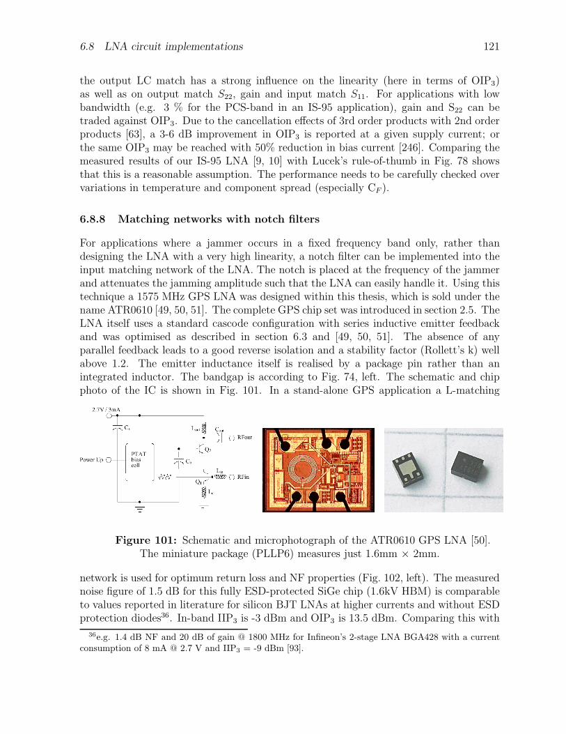
6.8 LNA circuit implementations 121
the output LC match has a strong influence on the linearity (here in terms of OIP3)as well as on output match S22, gain and input match S11. For applications with lowbandwidth (e.g. 3 % for the PCS-band in an IS-95 application), gain and S22 can betraded against OIP3. Due to the cancellation effects of 3rd order products with 2nd orderproducts [63], a 3-6 dB improvement in OIP3 is reported at a given supply current; orthe same OIP3 may be reached with 50% reduction in bias current [246]. Comparing themeasured results of our IS-95 LNA [9, 10] with Lucek’s rule-of-thumb in Fig. 78 showsthat this is a reasonable assumption. The performance needs to be carefully checked overvariations in temperature and component spread (especially CF ).
6.8.8 Matching networks with notch filters
For applications where a jammer occurs in a fixed frequency band only, rather thandesigning the LNA with a very high linearity, a notch filter can be implemented into theinput matching network of the LNA. The notch is placed at the frequency of the jammerand attenuates the jamming amplitude such that the LNA can easily handle it. Using thistechnique a 1575 MHz GPS LNA was designed within this thesis, which is sold under thename ATR0610 [49, 50, 51]. The complete GPS chip set was introduced in section 2.5. TheLNA itself uses a standard cascode configuration with series inductive emitter feedbackand was optimised as described in section 6.3 and [49, 50, 51]. The absence of anyparallel feedback leads to a good reverse isolation and a stability factor (Rollett’s k) wellabove 1.2. The emitter inductance itself is realised by a package pin rather than anintegrated inductor. The bandgap is according to Fig. 74, left. The schematic and chipphoto of the IC is shown in Fig. 101. In a stand-alone GPS application a L-matching
Figure 101: Schematic and microphotograph of the ATR0610 GPS LNA [50].The miniature package (PLLP6) measures just 1.6mm × 2mm.
network is used for optimum return loss and NF properties (Fig. 102, left). The measurednoise figure of 1.5 dB for this fully ESD-protected SiGe chip (1.6kV HBM) is comparableto values reported in literature for silicon BJT LNAs at higher currents and without ESDprotection diodes36. In-band IIP3 is -3 dBm and OIP3 is 13.5 dBm. Comparing this with
36e.g. 1.4 dB NF and 20 dB of gain @ 1800 MHz for Infineon’s 2-stage LNA BGA428 with a currentconsumption of 8 mA @ 2.7 V and IIP3 = -9 dBm [93].
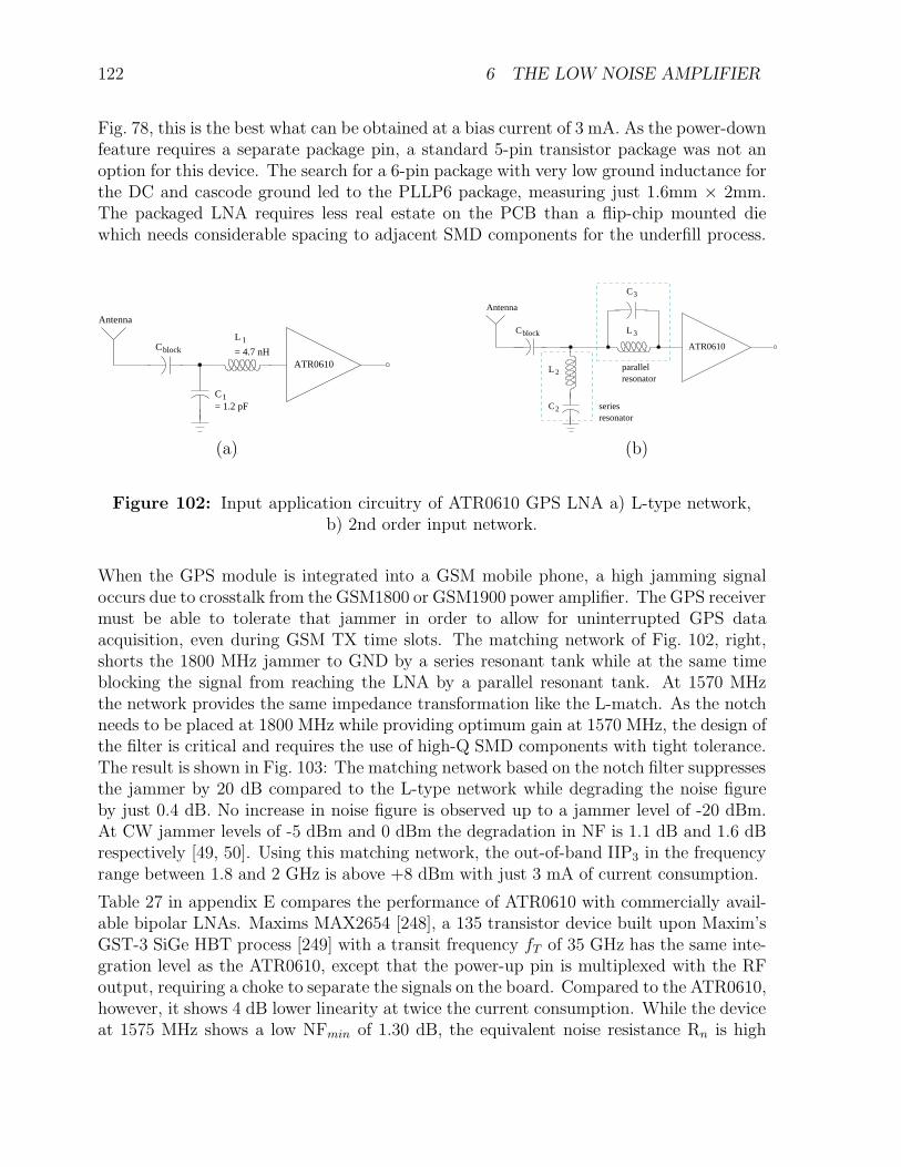
122 6 THE LOW NOISE AMPLIFIER
Fig. 78, this is the best what can be obtained at a bias current of 3 mA. As the power-downfeature requires a separate package pin, a standard 5-pin transistor package was not anoption for this device. The search for a 6-pin package with very low ground inductance forthe DC and cascode ground led to the PLLP6 package, measuring just 1.6mm × 2mm.The packaged LNA requires less real estate on the PCB than a flip-chip mounted diewhich needs considerable spacing to adjacent SMD components for the underfill process.
C1
Cblock
L 1
Antenna
ATR0610
= 1.2 pF
= 4.7 nH
L 3
C3
Cblock
C2
L 2parallelresonator
seriesresonator
ATR0610
Antenna
(a) (b)
Figure 102: Input application circuitry of ATR0610 GPS LNA a) L-type network,b) 2nd order input network.
When the GPS module is integrated into a GSM mobile phone, a high jamming signaloccurs due to crosstalk from the GSM1800 or GSM1900 power amplifier. The GPS receivermust be able to tolerate that jammer in order to allow for uninterrupted GPS dataacquisition, even during GSM TX time slots. The matching network of Fig. 102, right,shorts the 1800 MHz jammer to GND by a series resonant tank while at the same timeblocking the signal from reaching the LNA by a parallel resonant tank. At 1570 MHzthe network provides the same impedance transformation like the L-match. As the notchneeds to be placed at 1800 MHz while providing optimum gain at 1570 MHz, the design ofthe filter is critical and requires the use of high-Q SMD components with tight tolerance.The result is shown in Fig. 103: The matching network based on the notch filter suppressesthe jammer by 20 dB compared to the L-type network while degrading the noise figureby just 0.4 dB. No increase in noise figure is observed up to a jammer level of -20 dBm.At CW jammer levels of -5 dBm and 0 dBm the degradation in NF is 1.1 dB and 1.6 dBrespectively [49, 50]. Using this matching network, the out-of-band IIP3 in the frequencyrange between 1.8 and 2 GHz is above +8 dBm with just 3 mA of current consumption.
Table 27 in appendix E compares the performance of ATR0610 with commercially avail-able bipolar LNAs. Maxims MAX2654 [248], a 135 transistor device built upon Maxim’sGST-3 SiGe HBT process [249] with a transit frequency fT of 35 GHz has the same inte-gration level as the ATR0610, except that the power-up pin is multiplexed with the RFoutput, requiring a choke to separate the signals on the board. Compared to the ATR0610,however, it shows 4 dB lower linearity at twice the current consumption. While the deviceat 1575 MHz shows a low NFmin of 1.30 dB, the equivalent noise resistance Rn is high
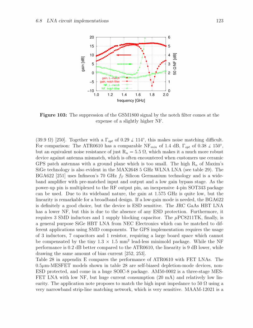
6.8 LNA circuit implementations 123
−10
−5
0
5
10
15
20
1.0 1.2 1.4 1.6 1.8 2.00
1
2
3
4
5
6
gain
[dB
]
50 Ω
NF
[dB
]
frequency [GHz]
gain, L−match
gain, notch filter
NF, L−match
NF, notch filter
Figure 103: The suppression of the GSM1800 signal by the notch filter comes at theexpense of a slightly higher NF.
(39.9 Ω) [250]. Together with a Γopt of 0.29 6 114, this makes noise matching difficult.For comparison: The ATR0610 has a comparable NFmin of 1.4 dB, Γopt of 0.38 6 150,but an equivalent noise resistance of just Rn = 5.5 Ω, which makes it a much more robustdevice against antenna mismatch, which is often encountered when customers use ceramicGPS patch antennas with a ground plane which is too small. The high Rn of Maxim’sSiGe technology is also evident in the MAX2648 5 GHz WLNA LNA (see table 29). TheBGA622 [251] uses Infineon’s 70 GHz fT Silicon Germanium technology and is a wide-band amplifier with pre-matched input and output and a low gain bypass stage. As thepower-up pin is multiplexed to the RF output pin, an inexpensive 4-pin SOT343 packagecan be used. Due to its wideband nature, the gain at 1.575 GHz is quite low, but thelinearity is remarkable for a broadband design. If a low-gain mode is needed, the BGA622is definitely a good choice, but the device is ESD sensitive. The JRC GaAs HBT LNAhas a lower NF, but this is due to the absence of any ESD protection. Furthermore, itrequires 3 SMD inductors and 1 supply blocking capacitor. The µPC8211TK, finally, isa general purpose SiGe HBT LNA from NEC Electronics which can be matched to dif-ferent applications using SMD components. The GPS implementation requires the usageof 3 inductors, 7 capacitors and 1 resistor, requiring a large board space which cannotbe compensated by the tiny 1.3 × 1.5 mm2 lead-less minimold package. While the NFperformance is 0.2 dB better compared to the ATR0610, the linearity is 9 dB lower, whiledrawing the same amount of bias current [252, 253].Table 28 in appendix E compares the performance of ATR0610 with FET LNAs. The0.5µm-MESFET models shown in table 28 are self-biased depletion-mode devices, non-ESD protected, and come in a huge SOIC-8 package. AM50-0002 is a three-stage MES-FET LNA with low NF, but huge current consumption (20 mA) and relatively low lin-earity. The application note proposes to match the high input impedance to 50 Ω using avery narrowband strip-line matching network, which is very sensitive. MAAM-12021 is a
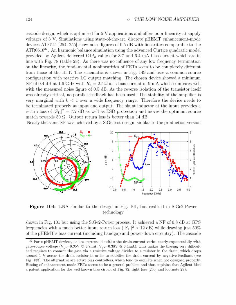
124 6 THE LOW NOISE AMPLIFIER
cascode design, which is optimised for 5 V applications and offers poor linearity at supplyvoltages of 3 V. Simulations using state-of-the-art, discrete pHEMT enhancement-modedevices ATF541 [254, 255] show noise figures of 0.5 dB with linearities comparable to theATR061037. An harmonic balance simulation using the advanced Curtice quadratic modelprovided by Agilent delivered OIP3 values for 3.7 and 6.4 mA bias current which are inline with Fig. 78 (table 28). As there was no influence of any low frequency terminationon the linearity, the fundamental nonlinearities of FETs seem to be completely differentfrom those of the BJT. The schematic is shown in Fig. 149 and uses a common-sourceconfiguration with reactive LC output matching. The chosen device showed a minimumNF of 0.4 dB at 1.6 GHz with Rn = 2.5 Ω at a bias current of 9 mA which compares wellwith the measured noise figure of 0.5 dB. As the reverse isolation of the transistor itselfwas already critical, no parallel feedback has been used: The stability of the amplifier isvery marginal with k < 1 over a wide frequency range. Therefore the device needs tobe terminated properly at input and output. The shunt inductor at the input provides areturn loss of |S11|2 = 7.2 dB as well as ESD protection and moves the optimum sourcematch towards 50 Ω. Output return loss is better than 14 dB.Nearly the same NF was achieved by a SiGe test design, similar to the production version
j0.3
j0.6
j1.0j1.5
j3.0
−j0.3
−j0.6
−j1.0−j1.5
−j3.0
0.15 0.3 0.6 1.0 1.5 3.00.0 8
j0.3
j0.6
j1.0j1.5
j3.0
−j0.3
−j0.6
−j1.0−j1.5
−j3.0
0.15 0.3 0.6 1.0 1.5 3.00.0 8
j0.3
j0.6
j1.0j1.5
j3.0
−j0.3
−j0.6
−j1.0−j1.5
−j3.0
0.15 0.3 0.6 1.0 1.5 3.00.0 8
j0.3
j0.6
j1.0j1.5
j3.0
−j0.3
−j0.6
−j1.0−j1.5
−j3.0
0.15 0.3 0.6 1.0 1.5 3.00.0 8
j0.3
j0.6
j1.0j1.5
j3.0
−j0.3
−j0.6
−j1.0−j1.5
−j3.0
0.15 0.3 0.6 1.0 1.5 3.00.0 8
j0.3
j0.6
j1.0j1.5
j3.0
−j0.3
−j0.6
−j1.0−j1.5
−j3.0
0.15 0.3 0.6 1.0 1.5 3.00.0 8
j0.3
j0.6
j1.0j1.5
j3.0
−j0.3
−j0.6
−j1.0−j1.5
−j3.0
0.15 0.3 0.6 1.0 1.5 3.00.0 8
j0.3
j0.6
j1.0j1.5
j3.0
−j0.3
−j0.6
−j1.0−j1.5
−j3.0
0.15 0.3 0.6 1.0 1.5 3.00.0 8
j0.3
j0.6
j1.0j1.5
j3.0
−j0.3
−j0.6
−j1.0−j1.5
−j3.0
0.15 0.3 0.6 1.0 1.5 3.00.0 8
j0.3
j0.6
j1.0j1.5
j3.0
−j0.3
−j0.6
−j1.0−j1.5
−j3.0
0.15 0.3 0.6 1.0 1.5 3.00.0 8
j0.3
j0.6
j1.0j1.5
j3.0
−j0.3
−j0.6
−j1.0−j1.5
−j3.0
0.15 0.3 0.6 1.0 1.5 3.00.0 8
j0.3
j0.6
j1.0j1.5
j3.0
−j0.3
−j0.6
−j1.0−j1.5
−j3.0
0.15 0.3 0.6 1.0 1.5 3.00.0 8
j0.3
j0.6
j1.0j1.5
j3.0
−j0.3
−j0.6
−j1.0−j1.5
−j3.0
0.15 0.3 0.6 1.0 1.5 3.00.0 8
j0.3
j0.6
j1.0j1.5
j3.0
−j0.3
−j0.6
−j1.0−j1.5
−j3.0
0.15 0.3 0.6 1.0 1.5 3.00.0 8
j0.3
j0.6
j1.0j1.5
j3.0
−j0.3
−j0.6
−j1.0−j1.5
−j3.0
0.15 0.3 0.6 1.0 1.5 3.00.0 8
j0.3
j0.6
j1.0j1.5
j3.0
−j0.3
−j0.6
−j1.0−j1.5
−j3.0
0.15 0.3 0.6 1.0 1.5 3.00.0 8
j0.3
j0.6
j1.0j1.5
j3.0
−j0.3
−j0.6
−j1.0−j1.5
−j3.0
0.15 0.3 0.6 1.0 1.5 3.00.0 8
j0.3
j0.6
j1.0j1.5
j3.0
−j0.3
−j0.6
−j1.0−j1.5
−j3.0
0.15 0.3 0.6 1.0 1.5 3.00.0 8
j0.3
j0.6
j1.0j1.5
j3.0
−j0.3
−j0.6
−j1.0−j1.5
−j3.0
0.15 0.3 0.6 1.0 1.5 3.00.0 8
S11S22
−10
−5
0
5
10
15
20
0.0 0.5 1.0 1.5 2.0 2.5 3.0 3.5 4.00
1
2
3
4
5
6
gain
[dB
]
50 Ω
NF
[dB
] and R
olle
t’s k
frequency [GHz]
S21
NF
k
Figure 104: LNA similar to the design in Fig. 101, but realized in SiGe2-Powertechnology
shown in Fig. 101 but using the SiGe2-Power process. It achieved a NF of 0.8 dB at GPSfrequencies with a much better input return loss (|S11|2 > 12 dB) while drawing just 50%of the pHEMT’s bias current (including bandgap and power-down circuitry). The cascode
37 For e-pHEMT devices, at low currents densities the drain current varies nearly exponentially withgate-source voltage (Vgs=0.35V @ 3.7mA, Vgs=0.38V @ 6.4mA). This makes the biasing very difficultand requires to connect the gate via a resistive voltage divider to a resistor in the drain, which dropsaround 1 V across the drain resistor in order to stabilise the drain current by negative feedback (seeFig. 133). The alternative are active bias controllers, which tend to oscillate when not designed properly.Biasing of enhancement mode FETs seems to be a general problem and thus explains that Agilent fileda patent application for the well known bias circuit of Fig. 72, right (see [230] and footnote 29).
6.8 LNA circuit implementations 125
RF stage with on-chip output match (|S22|2 > 14 dB) provided excellent stability. Usingthe GaAs pHEMT LNA instead of this advanced SiGe LNA would lead to 0.3 dB moreGPS sensitivity, however at the expense of stability and at twice the power consumption.Compared to the implementation losses of typical GPS antennas, the 0.3 dB difference insensitivity are negligible.These results show that SiGe HBT technology can deliver similar noise and linearity per-formance with better stability at lower supply voltages and lower current consumptionthan GaAs MESFET and pHEMT.
6.8.9 Comparison of the circuit design techniques for linearization enhance-ment
For the WLAN system described in section 2.4 a broad-band LNA was designed accordingto the specifications of table 22.
Frequency range 4.9 - 5.9 GHzNoise figure < 2 dBGain 10 dB (min.)P1dB,in -14 dBm (4.9-5.4 GHz)
-12 dBm (5.4-5.9 GHz)IIP3 -4 dBm (4.9-5.4 GHz)
0 dBm (5.4-5.9 GHz)Power consumption 7-8 mA @ 3V
Table 22: Target specification for the 4.9-5.9 GHz WLAN LNA [37].
Simulations using the SiGe2-RF design kit showed that the 2 dB NF is the main difficultyin reaching the specs of table 22, although Erben et al. [86, 92] in 1998 reached NFmin
values of 1.6 dB on-wafer at 5.7 GHz for a 2-stage common-emitter LNA using TEMIC’spre-production SiGe1 process. As discussed in section 2.4, a single-ended design wasrequested as its easier to interface to the TX/RX switch. For the required bandwidth of19%, a transimpedance stage would be appropriate, but the resistive feedback deterioratesthe NF and a resistive load at a supply voltage of 3 V strongly reduces linearity. A narrowband amplifier architecture has finally been chosen, with the Q of the LC matching reducedby a 500 Ω resistor to reach the required bandwidth. A simple common-emitter stageshowed the lowest noise figure, but at the band edge of 5.9 GHz delivered just 9.5 dB ofgain. Finally, a cascode structure was used as in [45], as it increased the NF by less than0.05 dB, but allowed for a higher gain margin. The common-emitter HBT is a 4-finger SICdevice (0.5 × 15µm2 each) which is cascaded by a 2-finger non-SIC device. For biasing,a PTAT bandgap based on the Widlar ∆VBE-cell was used similar to the one shown inFig. 74. Compared to the previous designs in Figs. 87, 94, 99, 101, however, the base ofthe cascode was not connected to a 1.4 V reference (2 diodes), but was connected directlyto the 2 V rail of the Widlar bandgap via a 1.5 kΩ / 3 pF low pass: Besides reducing the
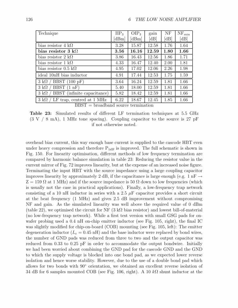
126 6 THE LOW NOISE AMPLIFIER
Technique IIP3 OIP3 gain NF NFmin
[dBm] [dBm] [dB] [dB] [dB]
bias resistor 4 kΩ 3.28 15.87 12.58 1.76 1.64bias resistor 3 kΩ 3.56 16.16 12.59 1.80 1.66bias resistor 2 kΩ 3.86 16.43 12.56 1.86 1.71bias resistor 1 kΩ 4.33 16.47 12.40 2.00 1.81bias resistor 0.5 kΩ 4.95 17.02 12.06 2.26 1.98
ideal 10nH bias inductor 4.91 17.44 12.53 1.75 1.59
3 kΩ / BBST (100 pF) 3.64 16.24 12.59 1.81 1.663 kΩ / BBST (1 nF) 5.40 18.00 12.59 1.81 1.663 kΩ / BBST (infinite capacitance) 5.82 18.42 12.59 1.81 1.66
3 kΩ / LF trap, centred at 1 MHz 6.22 18.67 12.45 1.85 1.66BBST = broadband source termination
Table 23: Simulated results of different LF termination techniques at 5.5 GHz(3 V / 8 mA), 1 MHz tone spacing). Coupling capacitor to the source is 27 pF
if not otherwise noted.
overhead bias current, this way enough base current is supplied to the cascode HBT evenunder heavy compression and therefore P1dB is improved. The full schematic is shown inFig. 150. For linearity optimisation, different methods of low frequency termination arecompared by harmonic balance simulation in table 23: Reducing the resistor value in thecurrent mirror of Fig. 72 improves linearity, but at the expense of an increased noise figure.Terminating the input HBT with the source impedance using a large coupling capacitorimproves linearity by approximately 2 dB, if the capacitance is large enough (e.g. 1 nF →Z = 159 Ω at 1 MHz) and if the source impedance is 50 Ω down to low frequencies (whichis usually not the case in practical applications). Finally, a low-frequency trap networkconsisting of a 10 nH inductor in series with a 2.5 µF capacitor provides a short circuitat the beat frequency (1 MHz) and gives 2.5 dB improvement without compromisingNF and gain. As the simulated linearity was well above the required value of 0 dBm(table 22), we optimised the circuit for NF (3 kΩ bias resistor) and lowest bill-of-material(no low-frequency trap network). While a first test version with small GSG pads for on-wafer probing used a 0.4 nH on-chip emitter inductor (see Fig. 105, right), the final ICwas slightly modified for chip-on-board (COB) mounting (see Fig. 105, left): The emitterdegeneration inductor (Le = 0.45 nH) and the base inductor were replaced by bond wires,the number of GND pads was reduced from three to two and the output capacitor wasreduced from 0.33 to 0.25 pF in order to accommodate the output bondwire. Initiallywe had been worried about combining the GND pad for the cascode GND and the GNDto which the supply voltage is blocked into one bond pad, as we expected lower reverseisolation and hence worse stability. However, due to the use of a double bond pad whichallows for two bonds with 90 orientation, we obtained an excellent reverse isolation of34 dB for 6 samples mounted COB (see Fig. 106, right). A 10 kΩ shunt inductor at the
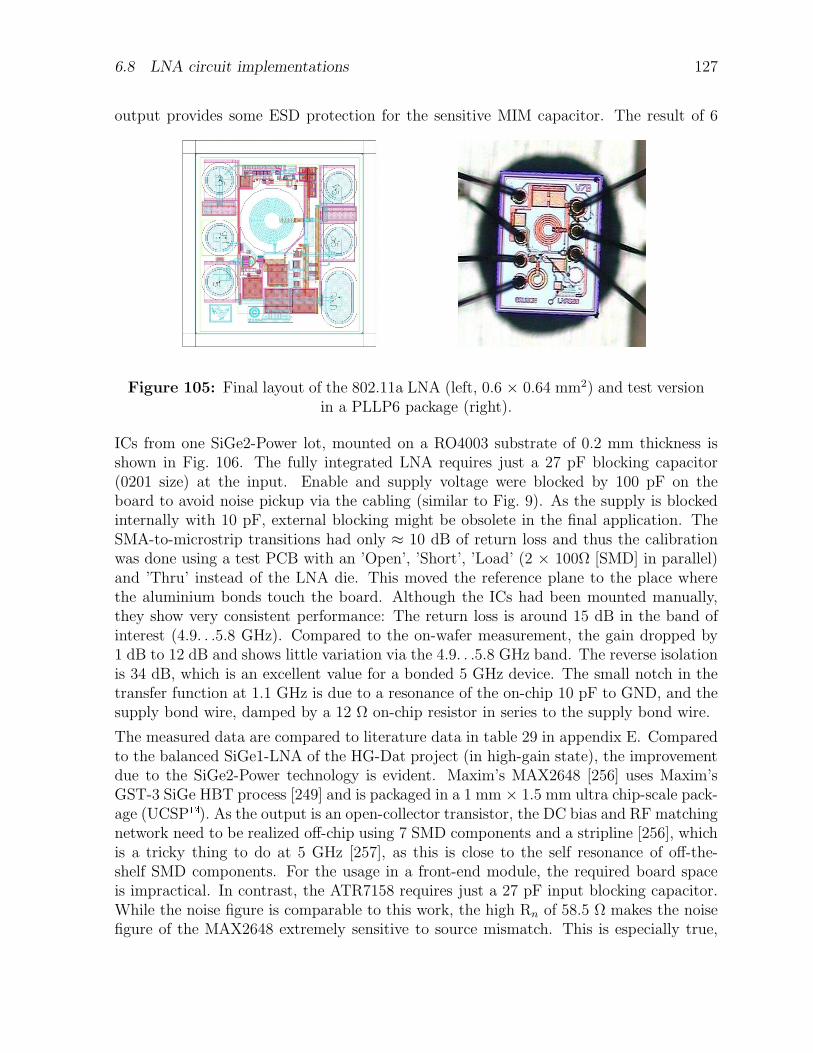
6.8 LNA circuit implementations 127
output provides some ESD protection for the sensitive MIM capacitor. The result of 6
Figure 105: Final layout of the 802.11a LNA (left, 0.6 × 0.64 mm2) and test versionin a PLLP6 package (right).
ICs from one SiGe2-Power lot, mounted on a RO4003 substrate of 0.2 mm thickness isshown in Fig. 106. The fully integrated LNA requires just a 27 pF blocking capacitor(0201 size) at the input. Enable and supply voltage were blocked by 100 pF on theboard to avoid noise pickup via the cabling (similar to Fig. 9). As the supply is blockedinternally with 10 pF, external blocking might be obsolete in the final application. TheSMA-to-microstrip transitions had only ≈ 10 dB of return loss and thus the calibrationwas done using a test PCB with an ’Open’, ’Short’, ’Load’ (2 × 100Ω [SMD] in parallel)and ’Thru’ instead of the LNA die. This moved the reference plane to the place wherethe aluminium bonds touch the board. Although the ICs had been mounted manually,they show very consistent performance: The return loss is around 15 dB in the band ofinterest (4.9. . .5.8 GHz). Compared to the on-wafer measurement, the gain dropped by1 dB to 12 dB and shows little variation via the 4.9. . .5.8 GHz band. The reverse isolationis 34 dB, which is an excellent value for a bonded 5 GHz device. The small notch in thetransfer function at 1.1 GHz is due to a resonance of the on-chip 10 pF to GND, and thesupply bond wire, damped by a 12 Ω on-chip resistor in series to the supply bond wire.
The measured data are compared to literature data in table 29 in appendix E. Comparedto the balanced SiGe1-LNA of the HG-Dat project (in high-gain state), the improvementdue to the SiGe2-Power technology is evident. Maxim’s MAX2648 [256] uses Maxim’sGST-3 SiGe HBT process [249] and is packaged in a 1 mm × 1.5 mm ultra chip-scale pack-age (UCSP). As the output is an open-collector transistor, the DC bias and RF matchingnetwork need to be realized off-chip using 7 SMD components and a stripline [256], whichis a tricky thing to do at 5 GHz [257], as this is close to the self resonance of off-the-shelf SMD components. For the usage in a front-end module, the required board spaceis impractical. In contrast, the ATR7158 requires just a 27 pF input blocking capacitor.While the noise figure is comparable to this work, the high Rn of 58.5 Ω makes the noisefigure of the MAX2648 extremely sensitive to source mismatch. This is especially true,
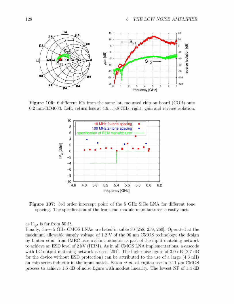
128 6 THE LOW NOISE AMPLIFIER
j0.3
j0.6
j1.0
j1.5
j3.0
−j0.3
−j0.6
−j1.0−j1.5
−j3.0
0.15 0.3 0.6 1.0 1.5 3.00.0 8
j0.3
j0.6
j1.0
j1.5
j3.0
−j0.3
−j0.6
−j1.0−j1.5
−j3.0
0.15 0.3 0.6 1.0 1.5 3.00.0 8
j0.3
j0.6
j1.0
j1.5
j3.0
−j0.3
−j0.6
−j1.0−j1.5
−j3.0
0.15 0.3 0.6 1.0 1.5 3.00.0 8
j0.3
j0.6
j1.0
j1.5
j3.0
−j0.3
−j0.6
−j1.0−j1.5
−j3.0
0.15 0.3 0.6 1.0 1.5 3.00.0 8
j0.3
j0.6
j1.0
j1.5
j3.0
−j0.3
−j0.6
−j1.0−j1.5
−j3.0
0.15 0.3 0.6 1.0 1.5 3.00.0 8
j0.3
j0.6
j1.0
j1.5
j3.0
−j0.3
−j0.6
−j1.0−j1.5
−j3.0
0.15 0.3 0.6 1.0 1.5 3.00.0 8
j0.3
j0.6
j1.0
j1.5
j3.0
−j0.3
−j0.6
−j1.0−j1.5
−j3.0
0.15 0.3 0.6 1.0 1.5 3.00.0 8
j0.3
j0.6
j1.0
j1.5
j3.0
−j0.3
−j0.6
−j1.0−j1.5
−j3.0
0.15 0.3 0.6 1.0 1.5 3.00.0 8
j0.3
j0.6
j1.0
j1.5
j3.0
−j0.3
−j0.6
−j1.0−j1.5
−j3.0
0.15 0.3 0.6 1.0 1.5 3.00.0 8
j0.3
j0.6
j1.0
j1.5
j3.0
−j0.3
−j0.6
−j1.0−j1.5
−j3.0
0.15 0.3 0.6 1.0 1.5 3.00.0 8
j0.3
j0.6
j1.0
j1.5
j3.0
−j0.3
−j0.6
−j1.0−j1.5
−j3.0
0.15 0.3 0.6 1.0 1.5 3.00.0 8
j0.3
j0.6
j1.0
j1.5
j3.0
−j0.3
−j0.6
−j1.0−j1.5
−j3.0
0.15 0.3 0.6 1.0 1.5 3.00.0 8
j0.3
j0.6
j1.0
j1.5
j3.0
−j0.3
−j0.6
−j1.0−j1.5
−j3.0
0.15 0.3 0.6 1.0 1.5 3.00.0 8
j0.3
j0.6
j1.0
j1.5
j3.0
−j0.3
−j0.6
−j1.0−j1.5
−j3.0
0.15 0.3 0.6 1.0 1.5 3.00.0 8
j0.3
j0.6
j1.0
j1.5
j3.0
−j0.3
−j0.6
−j1.0−j1.5
−j3.0
0.15 0.3 0.6 1.0 1.5 3.00.0 8
j0.3
j0.6
j1.0
j1.5
j3.0
−j0.3
−j0.6
−j1.0−j1.5
−j3.0
0.15 0.3 0.6 1.0 1.5 3.00.0 8
j0.3
j0.6
j1.0
j1.5
j3.0
−j0.3
−j0.6
−j1.0−j1.5
−j3.0
0.15 0.3 0.6 1.0 1.5 3.00.0 8
j0.3
j0.6
j1.0
j1.5
j3.0
−j0.3
−j0.6
−j1.0−j1.5
−j3.0
0.15 0.3 0.6 1.0 1.5 3.00.0 8
j0.3
j0.6
j1.0
j1.5
j3.0
−j0.3
−j0.6
−j1.0−j1.5
−j3.0
0.15 0.3 0.6 1.0 1.5 3.00.0 8
S11
S22
-25
-20
-15
-10
-5
0
5
10
15
0 1 2 3 4 5 6 7 8-120
-100
-80
-60
-40
-20
0
20
40
gain
[dB
]
revers
e isola
tion [dB
]
frequency [GHz]
S21
S12
Figure 106: 6 different ICs from the same lot, mounted chip-on-board (COB) onto0.2 mm-RO4003. Left: return loss at 4.9. . .5.8 GHz, right: gain and reverse isolation.
−10
−8
−6
−4
−2
0
2
4
6
8
10
4.6 4.8 5.0 5.2 5.4 5.6 5.8 6.0 6.2
IIP
3 [
dB
m]
frequency [GHz]
10 MHz 2−tone spacing
100 MHz 2−tone spacing
specification of FEM manufacturer
Figure 107: 3rd order intercept point of the 5 GHz SiGe LNA for different tonespacing. The specification of the front-end module manufacturer is easily met.
as Γopt is far from 50 Ω.Finally, three 5 GHz CMOS LNAs are listed in table 30 [258, 259, 260]. Operated at themaximum allowable supply voltage of 1.2 V of the 90 nm CMOS technology, the designby Linten et al. from IMEC uses a shunt inductor as part of the input matching networkto achieve an ESD level of 2 kV (HBM). As in all CMOS LNA implementations, a cascodewith LC output matching network is used [261]. The high noise figure of 3.0 dB (2.7 dBfor the device without ESD protection) can be attributed to the use of a large (4.3 nH)on-chip series inductor in the input match. Satou et al. of Fujitsu uses a 0.11 µm CMOSprocess to achieve 1.6 dB of noise figure with modest linearity. The lowest NF of 1.4 dB
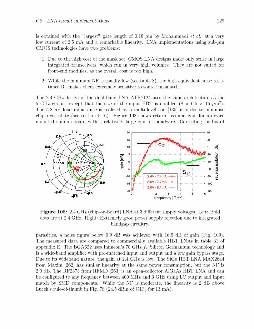
6.8 LNA circuit implementations 129
is obtained with the ”largest” gate length of 0.18 µm by Mohammadi et al. at a verylow current of 2.5 mA and a remarkable linearity. LNA implementations using sub-µmCMOS technologies have two problems:
1. Due to the high cost of the mask set, CMOS LNA designs make only sense in largeintegrated transceivers, which run in very high volumes. They are not suited forfront-end modules, as the overall cost is too high.
2. While the minimum NF is usually low (see table 8), the high equivalent noise resis-tance Rn makes them extremely sensitive to source mismatch.
The 2.4 GHz design of the dual-band LNA ATR7124 uses the same architecture as the5 GHz circuit, except that the size of the input HBT is doubled (8 × 0.5 × 15 µm2).The 5.8 nH load inductance is realized by a multi-level coil [135] in order to minimisechip real estate (see section 5.16). Figure 108 shows return loss and gain for a devicemounted chip-on-board with a relatively large emitter bondwire. Correcting for board
j0.3
j0.6
j1.0
j1.5
j3.0
−j0.3
−j0.6
−j1.0−j1.5
−j3.0
0.15 0.3 0.6 1.0 1.5 3.00.0 8
j0.3
j0.6
j1.0
j1.5
j3.0
−j0.3
−j0.6
−j1.0−j1.5
−j3.0
0.15 0.3 0.6 1.0 1.5 3.00.0 8
j0.3
j0.6
j1.0
j1.5
j3.0
−j0.3
−j0.6
−j1.0−j1.5
−j3.0
0.15 0.3 0.6 1.0 1.5 3.00.0 8
j0.3
j0.6
j1.0
j1.5
j3.0
−j0.3
−j0.6
−j1.0−j1.5
−j3.0
0.15 0.3 0.6 1.0 1.5 3.00.0 8
j0.3
j0.6
j1.0
j1.5
j3.0
−j0.3
−j0.6
−j1.0−j1.5
−j3.0
0.15 0.3 0.6 1.0 1.5 3.00.0 8
j0.3
j0.6
j1.0
j1.5
j3.0
−j0.3
−j0.6
−j1.0−j1.5
−j3.0
0.15 0.3 0.6 1.0 1.5 3.00.0 8
j0.3
j0.6
j1.0
j1.5
j3.0
−j0.3
−j0.6
−j1.0−j1.5
−j3.0
0.15 0.3 0.6 1.0 1.5 3.00.0 8
j0.3
j0.6
j1.0
j1.5
j3.0
−j0.3
−j0.6
−j1.0−j1.5
−j3.0
0.15 0.3 0.6 1.0 1.5 3.00.0 8
j0.3
j0.6
j1.0
j1.5
j3.0
−j0.3
−j0.6
−j1.0−j1.5
−j3.0
0.15 0.3 0.6 1.0 1.5 3.00.0 8
j0.3
j0.6
j1.0
j1.5
j3.0
−j0.3
−j0.6
−j1.0−j1.5
−j3.0
0.15 0.3 0.6 1.0 1.5 3.00.0 8
j0.3
j0.6
j1.0
j1.5
j3.0
−j0.3
−j0.6
−j1.0−j1.5
−j3.0
0.15 0.3 0.6 1.0 1.5 3.00.0 8
j0.3
j0.6
j1.0
j1.5
j3.0
−j0.3
−j0.6
−j1.0−j1.5
−j3.0
0.15 0.3 0.6 1.0 1.5 3.00.0 8
j0.3
j0.6
j1.0
j1.5
j3.0
−j0.3
−j0.6
−j1.0−j1.5
−j3.0
0.15 0.3 0.6 1.0 1.5 3.00.0 8
j0.3
j0.6
j1.0
j1.5
j3.0
−j0.3
−j0.6
−j1.0−j1.5
−j3.0
0.15 0.3 0.6 1.0 1.5 3.00.0 8
j0.3
j0.6
j1.0
j1.5
j3.0
−j0.3
−j0.6
−j1.0−j1.5
−j3.0
0.15 0.3 0.6 1.0 1.5 3.00.0 8
j0.3
j0.6
j1.0
j1.5
j3.0
−j0.3
−j0.6
−j1.0−j1.5
−j3.0
0.15 0.3 0.6 1.0 1.5 3.00.0 8
j0.3
j0.6
j1.0
j1.5
j3.0
−j0.3
−j0.6
−j1.0−j1.5
−j3.0
0.15 0.3 0.6 1.0 1.5 3.00.0 8
j0.3
j0.6
j1.0
j1.5
j3.0
−j0.3
−j0.6
−j1.0−j1.5
−j3.0
0.15 0.3 0.6 1.0 1.5 3.00.0 8
j0.3
j0.6
j1.0
j1.5
j3.0
−j0.3
−j0.6
−j1.0−j1.5
−j3.0
0.15 0.3 0.6 1.0 1.5 3.00.0 8
S11
S22
-20
-15
-10
-5
0
5
10
15
20
0 1 2 3 4 5 6-120
-100
-80
-60
-40
-20
0
20
40
gain
[dB
]
revers
e isola
tion [dB
]
frequency [GHz]
S21
S122.4V / 7.4mA
3.0V / 7.7mA
5.0V / 8.1mA
Figure 108: 2.4 GHz (chip-on-board) LNA at 3 different supply voltages. Left: Bolddots are at 2.4 GHz. Right: Extremely good power supply rejection due to integrated
bandgap circuitry.
parasitics, a noise figure below 0.9 dB was achieved with 16.5 dB of gain (Fig. 109).The measured data are compared to commercially available HBT LNAs in table 31 ofappendix E. The BGA622 uses Infineon’s 70 GHz fT Silicon Germanium technology andis a wide-band amplifier with pre-matched input and output and a low gain bypass stage.Due to its wideband nature, the gain at 2.4 GHz is low. The SiGe HBT LNA MAX2644from Maxim [262] has similar linearity at the same power consumption, but the NF is2.0 dB. The RF2373 from RFMD [263] is an open-collector AlGaAs HBT LNA and canbe configured to any frequency between 400 MHz and 3 GHz using LC output and inputmatch by SMD components. While the NF is moderate, the linearity is 2 dB aboveLucek’s rule-of-thumb in Fig. 78 (24.5 dBm of OIP3 for 13 mA).
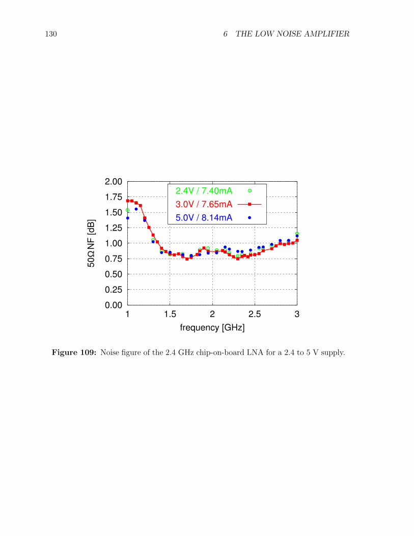
130 6 THE LOW NOISE AMPLIFIER
0.00
0.25
0.50
0.75
1.00
1.25
1.50
1.75
2.00
1 1.5 2 2.5 3
50
Ω N
F [dB
]
frequency [GHz]
2.4V / 7.40mA
3.0V / 7.65mA
5.0V / 8.14mA
Figure 109: Noise figure of the 2.4 GHz chip-on-board LNA for a 2.4 to 5 V supply.
131
7 The downconverter
7.1 Super-hetero and direct-conversion receivers
Since the invention of the superheterodyne receiver38 by Walter Schottky of Siemens in1918 [94] and Edwin Armstrong in 1920 [261], radio front-ends make extensive use offrequency downconversion from radio frequency transmitted over the air to an intermedi-ate frequency (IF). At this early level in the front-end there is no fundamental differencewhether the input signal is modulated in an analog fashion or a digital one. The IF fre-quency is usually fixed which allows for the use of a very steep passive filter using ceramicresonators or filters based on surface-acoustic-wave (SAW), film-bulk-acoustic-resonator(FBAR) or bulk-acoustic-wave (BAW) technology [70, 71, 72]. To downconvert one ofthe various RF channels of the system, the local oscillator is stepped across the channelsusing a voltage-controlled oscillator (VCO) which is locked to a quartz reference using aphase-locked-loop (PLL) circuit. A direct conversion receiver (DCR) downconverts themodulated RF signal directly to baseband, eliminating the need for an IF SAW filter atthe expense of power-hungry active base band (BB) filtering. DCRs are more difficult toimplement due to the following problem [264, 265]: In a superheterodyne receiver, DC offset – generated by imperfections in the mixer –
can easily be removed by AC coupling. In a DCR – as the VCO runs at the RF centre frequency – LO signal leakingback through the mixer and the LNA to the antenna is reflected at a mismatchedantenna, fed back via the LNA to the mixer and downconverted; leading to a DCoffset at the output of the mixer (self-mixing). This high amount of DC offset oftencannot be removed by AC coupling but needs an active DC offset canceler resultingin increased power consumption [265]. This problem of self-mixing is reduced byusing a LNA with a high reverse isolation (see section 6.8.4), a mixer with a highLO-to-RF isolation and a careful PCB design.
In the transmit path the mixer modulates the baseband signals back onto a RF carrier.This upconversion process can be a direct one (direct conversion) or take place via anIF frequency which allows for additional filtering before the final upconversion to RFhappens. IQ modulators are usually used in digitally modulated systems.In most of the systems described in this thesis, the superheterodyne approach has beenfavoured over the DCR: Narrowband CDMA (IS95), as described in sections 2.2.2, 2.2.3, and 3, is a challeng-
ing system, and some phones even today still use a superhet receiver. The reasonsare (i) strong blockers, after passing a highly linear LNA and mixer frontend, may
38Superheterodyne receiver: Radio receiver that converts all radio frequencies to a fixed intermediatefrequency to maximise gain and bandwidth before demodulation.
132 7 THE DOWNCONVERTER
be filtered easier using an IF compared to doing so at base band frequencies (ii)the small channel bandwidth does not allow for the removal of the DC offset byAC coupling (as it is the case in UMTS receivers), and finally (iii) the superhethas always a lower power consumption, as filtering is done on the IF using passivefilters, rather than using active filters at BB frequencies. Professional mobile radios (section 2.3) are high-performance devices with very highlinearity requirements, while cost is a minor issue. As has been described in section 2.5, the GPS signal is well below the noise floorand needs to be amplified – despite the high coding gain – at RF and IF frequencies.To the author’s knowledge, no GPS DCR has been reported so far. Two superhetarchitectures are currently used: The double conversion receiver with 2 IF frequen-cies and the single conversion receiver with direct subsampling at the IF. Due toits very low power consumption, the latter is used in Atmel’s ANTARISGPS chipset, despite the high NF associated with the subsampling architecture [261]. In UMTS, described in sections 2.2.4, DCRs dominate over the superhet in mobiledevices. Also the base station receiver, developed within the SCUBA framework,uses DCR in order to down-convert 4 channels simultaneously (see Fig. 4). Due to the price war for WLAN (section 2.4) devices, most of the solutions on themarket use a DCR architecture, with a trend to an all-CMOS implementation.
Frequency mixers are key components in both superhets and DCRs. The first implemen-tations used a single vacuum tube to realize oscillator, mixer and amplifier in a singledevice (e.g. Armstrong [261]), a technique which is still applied using IMPATT or Gunndiodes at sub-millimetre frequencies. Also the first transistor radio, the Regency TR1used this approach in order to minimise the usage of the expensive Ge transistors [261].In the next section we will have a look on the fundamentals of mixing operation, classifymixers in non-linear and commutating devices and give some examples.
7.2 Mixing operation
Using simple trigonometric analysis, a frequency converter (”mixer”) analytically is oftentreated to be a multiplier:
VIF = ARF · sin(2 · π · fRF · t) × ALO · cos(2 · π · fLO · t)= ARF × ALO · [sin(2 · π · [fRF − fLO] · t) + sin(2 · π · [fRF + fLO] · t)] (95)
An ideal mixer generates the difference and the sum of the input frequencies, while sup-pressing the input frequencies completely. In a down-conversion mixer, the sum of theinput frequencies, fRF + fLO, is usually easily suppressed by low-pass filtering. WhileEqn. 95 is a handy expression, it strictly only holds for frequency multipliers, where the
7.3 Mixers utilising device nonlinearities 133
output amplitude is proportional to the product of the input amplitudes. Such devicesdo exist as products, but they suffer from a low conversion gain and a high noise figureand are rarely used. Mixers, on the other hand, should be as ”linear” as possible in thesense that doubling the amplitude of the input signal exactly doubles the amplitude ofthe output frequency, but they should be insensitive to variations in LO amplitude inorder to get rid of both AM noise and amplitude variations of the VCO. Eqn. 95 thereforecan only give an indication of how a mixer works. The difference between a mixer and amultiplier is graphically shown in Fig. 110.
7.3 Mixers utilising device nonlinearities
While a mixer should be linear in amplitude from RF to IF, it cannot be built upon asingle linear element, as a linear circuit cannot lead to frequency conversion. Thereforefrequency conversion is often referred to as being a nonlinear process, making use of thenonlinear transfer function of a semiconductor device. This is true for a first kind ofmixer often used in the design of MMIC mixers at elevated frequencies, exploiting thenonlinearities of Schottky diodes, MESFETs or HEMTs. Three-port device mixers asshown in Fig. 112 have advantages over diode mixers here, including higher conversiongain, wider dynamic range, and better isolation between the ports [266]. The cascodeMESFET mixer [267] as shown in Fig. 112, right, is suited for low frequency applications,as it does not need passive couplers: The LO is usually fed to the gate of the upperFET (or the 2nd gate of a dual-gate device) and the RF is fed to the gate of the lowerFET. The IF can be deduced from the drain. Fuente et al. reported high conversiongain (13 dB) and high linearity (IIP3 = 7 dBm) along with 20 dB port-to-port isolationfor a 600 - 1800 MHz mixer with +7 dBm of LO drive using 0.5 µm × 300 µm GaAsMESFETs [267]. NF and power consumption were not reported.
7.4 Switching mixers
A simple switching mixer has been proposed by Maas [65]: It consists of a single FET,operated in resistive mode (VDS = 0). The LO is fed to the gate and switches the FETON and OFF periodically. RF is feed to the drain and at the same node the IF is deduced.When the LO signal is ”high”, the FET provides a short circuit at the drain, when the LOsignal is ”low”, the FET is in its high impedance state. In the ideal case, the FET wouldresemble a pure relay (0 Ω in ON state, no shunt capacitance in OFF mode). The circuitcan be operated single-ended and does not need any transformers or baluns. A GaAsimplementation for a 500 - 2500 MHz mixer reached 5.7 dB conversion loss, +24 dBm ofIIP3 and 6 dB of NF at a power consumption of 6 mA at 3 V [268]. As already pointedout by Maas [65], the difficulty is in the realisation of the matching networks. As RF andIF are both taken from the drain node, the mixer cannot provide isolation between them.Maas recommends to provide a short circuit for the LO frequency at the drain, whichis difficult to realise as fLO ≈ fRF . Instead, following [268], we used a series resonant
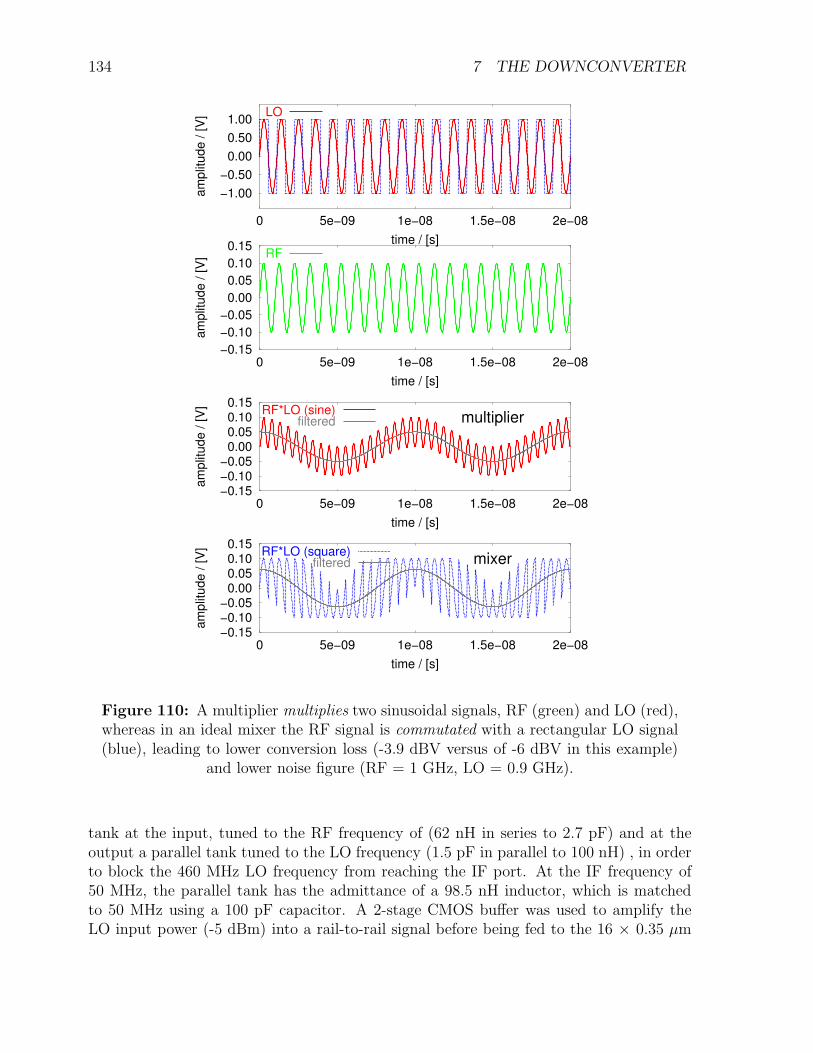
134 7 THE DOWNCONVERTER
−1.00
−0.50
0.00
0.50
1.00
0 5e−09 1e−08 1.5e−08 2e−08
am
plit
ude / [V
]
time / [s]
LO
−0.15
−0.10
−0.05
0.00
0.05
0.10
0.15
0 5e−09 1e−08 1.5e−08 2e−08
am
plit
ude / [V
]
time / [s]
RF
−0.15−0.10−0.05
0.000.050.100.15
0 5e−09 1e−08 1.5e−08 2e−08
am
plit
ude / [V
]
time / [s]
multiplierRF*LO (sine)
filtered
−0.15−0.10−0.05
0.000.050.100.15
0 5e−09 1e−08 1.5e−08 2e−08
am
plit
ude / [V
]
time / [s]
mixerRF*LO (square)
filtered
Figure 110: A multiplier multiplies two sinusoidal signals, RF (green) and LO (red),whereas in an ideal mixer the RF signal is commutated with a rectangular LO signal(blue), leading to lower conversion loss (-3.9 dBV versus of -6 dBV in this example)
and lower noise figure (RF = 1 GHz, LO = 0.9 GHz).
tank at the input, tuned to the RF frequency of (62 nH in series to 2.7 pF) and at theoutput a parallel tank tuned to the LO frequency (1.5 pF in parallel to 100 nH) , in orderto block the 460 MHz LO frequency from reaching the IF port. At the IF frequency of50 MHz, the parallel tank has the admittance of a 98.5 nH inductor, which is matchedto 50 MHz using a 100 pF capacitor. A 2-stage CMOS buffer was used to amplify theLO input power (-5 dBm) into a rail-to-rail signal before being fed to the 16 × 0.35 µm
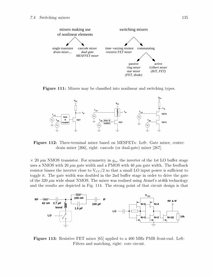
7.4 Switching mixers 135
mixers making use switching mixers
commutating
activepassive
of nonlinear elements
cascode mixersingle transistor time−varying resistorresistive FET mixer
MESFFET mixerdual gatedrain mixer,...
(BJT, FET)Gilbert mixer
(FET, diode)star mixerring mixer
Figure 111: Mixers may be classified into nonlinear and switching types.
VCC
VCCVCC
&coupler
bias &match
coup
ler
IF
bias
LO
f LO
f RF
f IF
f
f
f
RF RF
f LO
f
f IF
FET2
FET1FET
FET
Figure 112: Three-terminal mixer based on MESFETs: Left: Gate mixer, centre:drain mixer [266], right: cascode (or dual-gate) mixer [267].
× 20 µm NMOS transistor. For symmetry in gm, the inverter of the 1st LO buffer stageuses a NMOS with 20 µm gate width and a PMOS with 40 µm gate width. The feedbackresistor biases the inverter close to VCC/2 so that a small LO input power is sufficient totoggle it. The gate width was doubled in the 2nd buffer stage in order to drive the gateof the 320 µm wide shunt NMOS. The mixer was realised using Atmel’s at46k technologyand the results are depicted in Fig. 114. The strong point of that circuit design is that
62 nH 2.7 pF
100 nH
1.5 pF
100 pFbond
RF IF
LO
V
LO
10k
CC
RF & IF
N=1
N=2 N=4
N=2 N=16
Figure 113: Resistive FET mixer [65] applied to a 400 MHz PMR front-end. Left:Filters and matching, right: core circuit.
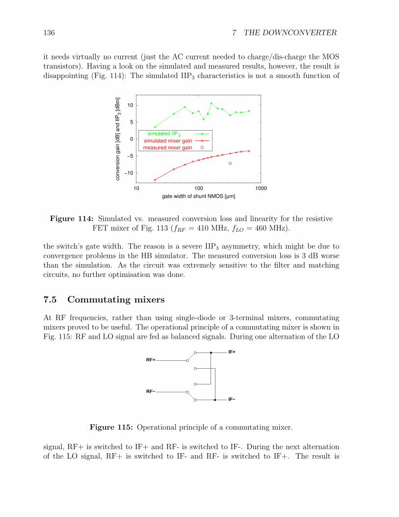
136 7 THE DOWNCONVERTER
it needs virtually no current (just the AC current needed to charge/dis-charge the MOStransistors). Having a look on the simulated and measured results, however, the result isdisappointing (Fig. 114): The simulated IIP3 characteristics is not a smooth function of
−10
−5
0
5
10
10 100 1000
convers
ion g
ain
[dB
] and IIP
3 [dB
m]
gate width of shunt NMOS [µm]
simulated IIP3
simulated mixer gain
measured mixer gain
Figure 114: Simulated vs. measured conversion loss and linearity for the resistiveFET mixer of Fig. 113 (fRF = 410 MHz, fLO = 460 MHz).
the switch’s gate width. The reason is a severe IIP3 asymmetry, which might be due toconvergence problems in the HB simulator. The measured conversion loss is 3 dB worsethan the simulation. As the circuit was extremely sensitive to the filter and matchingcircuits, no further optimisation was done.
7.5 Commutating mixers
At RF frequencies, rather than using single-diode or 3-terminal mixers, commutatingmixers proved to be useful. The operational principle of a commutating mixer is shown inFig. 115: RF and LO signal are fed as balanced signals. During one alternation of the LO
IF+
IF−
RF−
RF+
Figure 115: Operational principle of a commutating mixer.
signal, RF+ is switched to IF+ and RF- is switched to IF-. During the next alternationof the LO signal, RF+ is switched to IF- and RF- is switched to IF+. The result is
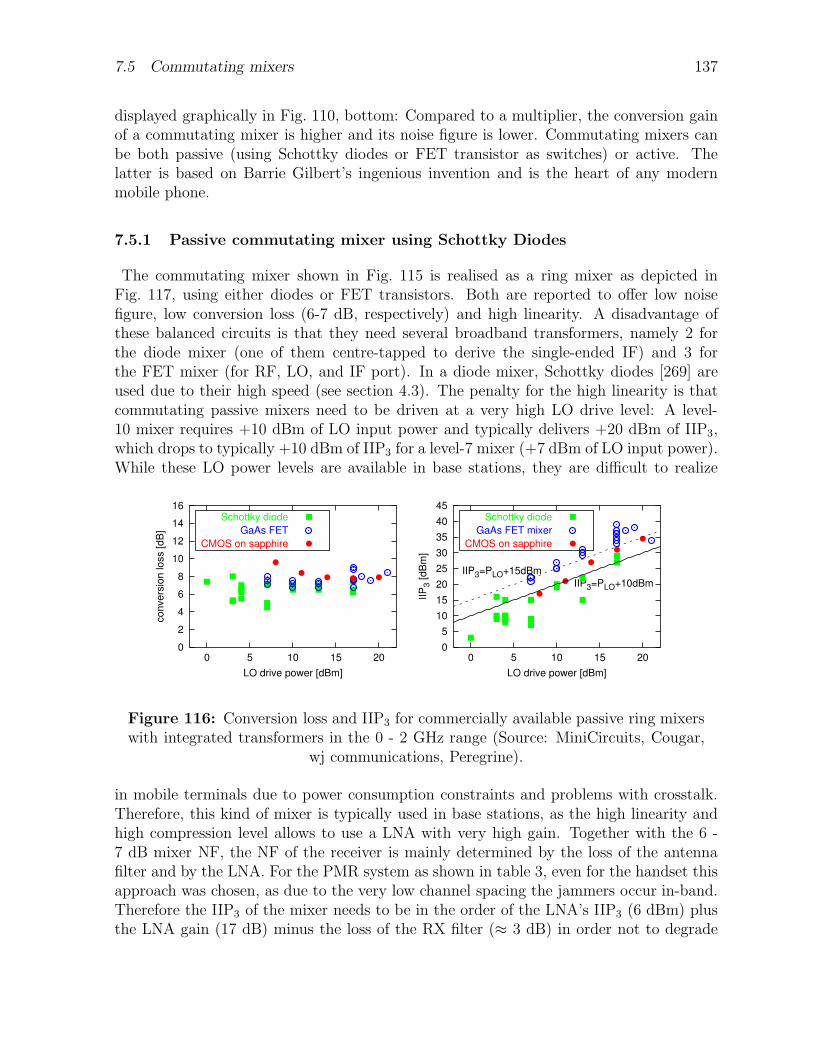
7.5 Commutating mixers 137
displayed graphically in Fig. 110, bottom: Compared to a multiplier, the conversion gainof a commutating mixer is higher and its noise figure is lower. Commutating mixers canbe both passive (using Schottky diodes or FET transistor as switches) or active. Thelatter is based on Barrie Gilbert’s ingenious invention and is the heart of any modernmobile phone.
7.5.1 Passive commutating mixer using Schottky Diodes
The commutating mixer shown in Fig. 115 is realised as a ring mixer as depicted inFig. 117, using either diodes or FET transistors. Both are reported to offer low noisefigure, low conversion loss (6-7 dB, respectively) and high linearity. A disadvantage ofthese balanced circuits is that they need several broadband transformers, namely 2 forthe diode mixer (one of them centre-tapped to derive the single-ended IF) and 3 forthe FET mixer (for RF, LO, and IF port). In a diode mixer, Schottky diodes [269] areused due to their high speed (see section 4.3). The penalty for the high linearity is thatcommutating passive mixers need to be driven at a very high LO drive level: A level-10 mixer requires +10 dBm of LO input power and typically delivers +20 dBm of IIP3,which drops to typically +10 dBm of IIP3 for a level-7 mixer (+7 dBm of LO input power).While these LO power levels are available in base stations, they are difficult to realize
0
2
4
6
8
10
12
14
16
0 5 10 15 20
convers
ion loss [dB
]
LO drive power [dBm]
Schottky diode
GaAs FET
CMOS on sapphire
0
5
10
15
20
25
30
35
40
45
0 5 10 15 20
IIP
3 [dB
m]
LO drive power [dBm]
IIP3=PLO+10dBm
IIP3=PLO+15dBm
Schottky diode
GaAs FET mixer
CMOS on sapphire
Figure 116: Conversion loss and IIP3 for commercially available passive ring mixerswith integrated transformers in the 0 - 2 GHz range (Source: MiniCircuits, Cougar,
wj communications, Peregrine).
in mobile terminals due to power consumption constraints and problems with crosstalk.Therefore, this kind of mixer is typically used in base stations, as the high linearity andhigh compression level allows to use a LNA with very high gain. Together with the 6 -7 dB mixer NF, the NF of the receiver is mainly determined by the loss of the antennafilter and by the LNA. For the PMR system as shown in table 3, even for the handset thisapproach was chosen, as due to the very low channel spacing the jammers occur in-band.Therefore the IIP3 of the mixer needs to be in the order of the LNA’s IIP3 (6 dBm) plusthe LNA gain (17 dB) minus the loss of the RX filter (≈ 3 dB) in order not to degrade
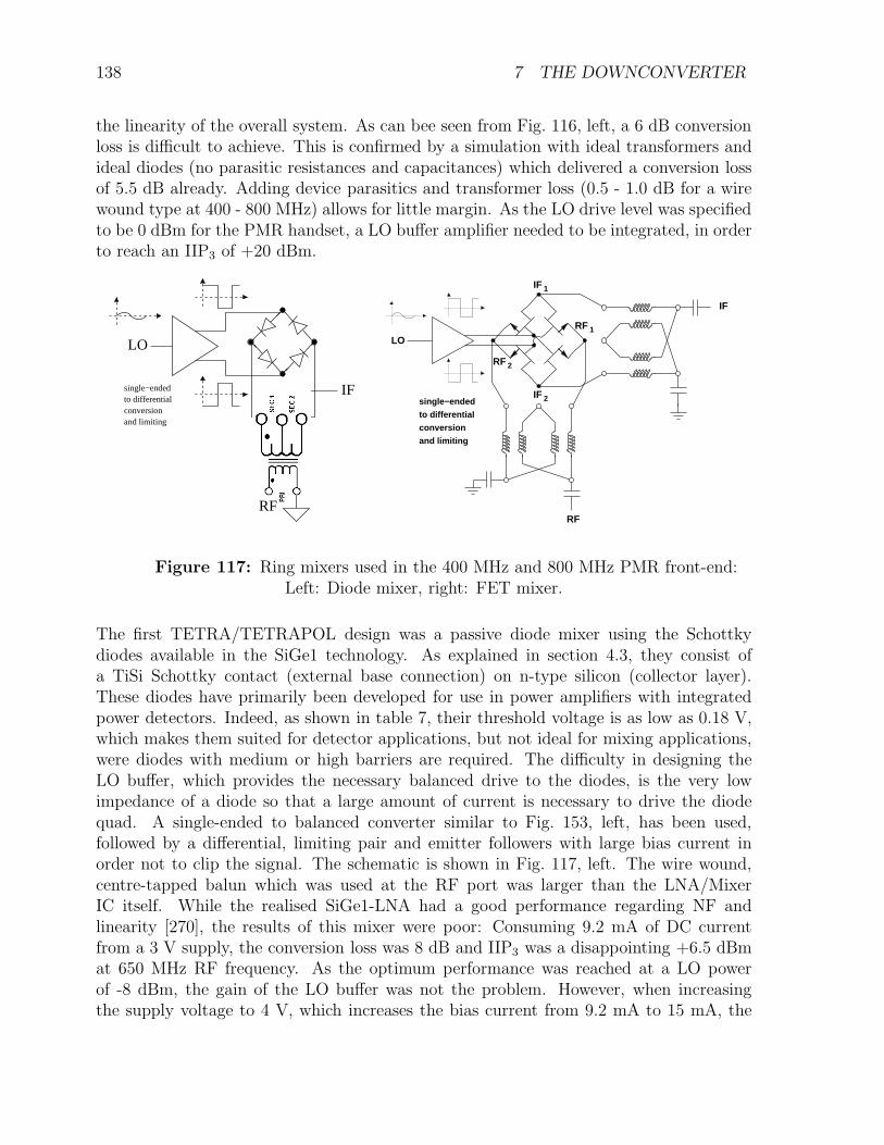
138 7 THE DOWNCONVERTER
the linearity of the overall system. As can bee seen from Fig. 116, left, a 6 dB conversionloss is difficult to achieve. This is confirmed by a simulation with ideal transformers andideal diodes (no parasitic resistances and capacitances) which delivered a conversion lossof 5.5 dB already. Adding device parasitics and transformer loss (0.5 - 1.0 dB for a wirewound type at 400 - 800 MHz) allows for little margin. As the LO drive level was specifiedto be 0 dBm for the PMR handset, a LO buffer amplifier needed to be integrated, in orderto reach an IIP3 of +20 dBm.
RF
IF
LO
single−endedto differentialconversionand limiting
IF 1
RF 1
RF 2
and limiting
conversion
single−endedIF 2
IF
LO
to differential
RF
Figure 117: Ring mixers used in the 400 MHz and 800 MHz PMR front-end:Left: Diode mixer, right: FET mixer.
The first TETRA/TETRAPOL design was a passive diode mixer using the Schottkydiodes available in the SiGe1 technology. As explained in section 4.3, they consist ofa TiSi Schottky contact (external base connection) on n-type silicon (collector layer).These diodes have primarily been developed for use in power amplifiers with integratedpower detectors. Indeed, as shown in table 7, their threshold voltage is as low as 0.18 V,which makes them suited for detector applications, but not ideal for mixing applications,were diodes with medium or high barriers are required. The difficulty in designing theLO buffer, which provides the necessary balanced drive to the diodes, is the very lowimpedance of a diode so that a large amount of current is necessary to drive the diodequad. A single-ended to balanced converter similar to Fig. 153, left, has been used,followed by a differential, limiting pair and emitter followers with large bias current inorder not to clip the signal. The schematic is shown in Fig. 117, left. The wire wound,centre-tapped balun which was used at the RF port was larger than the LNA/MixerIC itself. While the realised SiGe1-LNA had a good performance regarding NF andlinearity [270], the results of this mixer were poor: Consuming 9.2 mA of DC currentfrom a 3 V supply, the conversion loss was 8 dB and IIP3 was a disappointing +6.5 dBmat 650 MHz RF frequency. As the optimum performance was reached at a LO powerof -8 dBm, the gain of the LO buffer was not the problem. However, when increasingthe supply voltage to 4 V, which increases the bias current from 9.2 mA to 15 mA, the
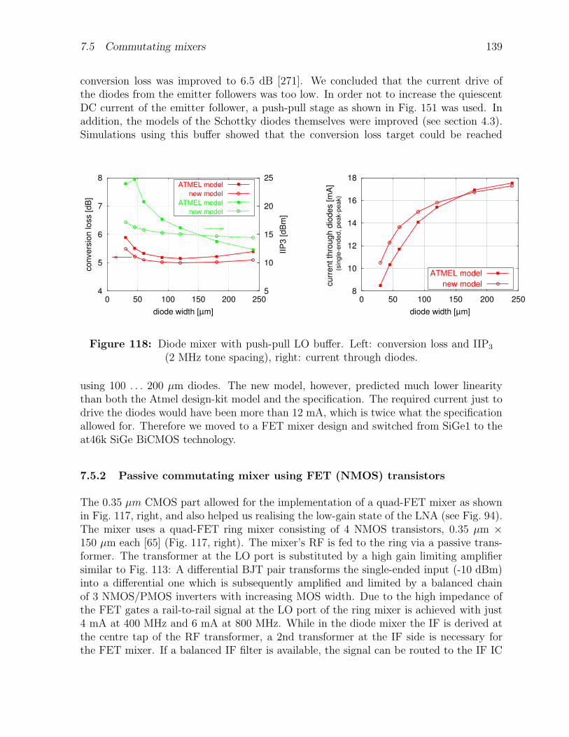
7.5 Commutating mixers 139
conversion loss was improved to 6.5 dB [271]. We concluded that the current drive ofthe diodes from the emitter followers was too low. In order not to increase the quiescentDC current of the emitter follower, a push-pull stage as shown in Fig. 151 was used. Inaddition, the models of the Schottky diodes themselves were improved (see section 4.3).Simulations using this buffer showed that the conversion loss target could be reached
4
5
6
7
8
0 50 100 150 200 2505
10
15
20
25
convers
ion loss [dB
]
IIP
3 [dB
m]
diode width [µm]
ATMEL model
new model
ATMEL model
new model
8
10
12
14
16
18
0 50 100 150 200 250
curr
ent th
rough d
iodes [m
A]
(sin
gle
-en
de
d,
pe
ak-p
ea
k)
diode width [µm]
ATMEL model
new model
Figure 118: Diode mixer with push-pull LO buffer. Left: conversion loss and IIP3
(2 MHz tone spacing), right: current through diodes.
using 100 . . . 200 µm diodes. The new model, however, predicted much lower linearitythan both the Atmel design-kit model and the specification. The required current just todrive the diodes would have been more than 12 mA, which is twice what the specificationallowed for. Therefore we moved to a FET mixer design and switched from SiGe1 to theat46k SiGe BiCMOS technology.
7.5.2 Passive commutating mixer using FET (NMOS) transistors
The 0.35 µm CMOS part allowed for the implementation of a quad-FET mixer as shownin Fig. 117, right, and also helped us realising the low-gain state of the LNA (see Fig. 94).The mixer uses a quad-FET ring mixer consisting of 4 NMOS transistors, 0.35 µm ×150 µm each [65] (Fig. 117, right). The mixer’s RF is fed to the ring via a passive trans-former. The transformer at the LO port is substituted by a high gain limiting amplifiersimilar to Fig. 113: A differential BJT pair transforms the single-ended input (-10 dBm)into a differential one which is subsequently amplified and limited by a balanced chainof 3 NMOS/PMOS inverters with increasing MOS width. Due to the high impedance ofthe FET gates a rail-to-rail signal at the LO port of the ring mixer is achieved with just4 mA at 400 MHz and 6 mA at 800 MHz. While in the diode mixer the IF is derived atthe centre tap of the RF transformer, a 2nd transformer at the IF side is necessary forthe FET mixer. If a balanced IF filter is available, the signal can be routed to the IF IC
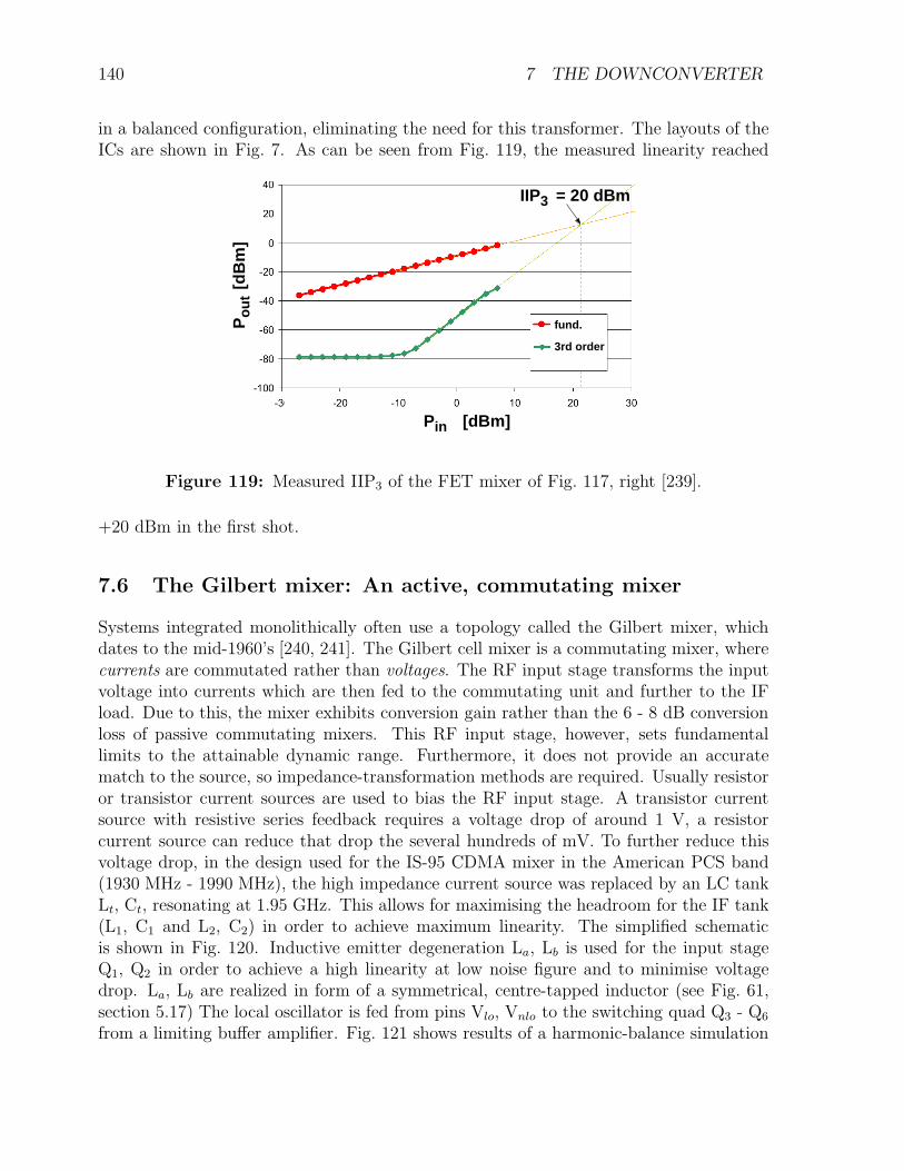
140 7 THE DOWNCONVERTER
in a balanced configuration, eliminating the need for this transformer. The layouts of theICs are shown in Fig. 7. As can be seen from Fig. 119, the measured linearity reached
Pin [dBm]
IIP3 = 20 dBm
[dB
m]
Pou
t
3rd order
fund.
Figure 119: Measured IIP3 of the FET mixer of Fig. 117, right [239].
+20 dBm in the first shot.
7.6 The Gilbert mixer: An active, commutating mixer
Systems integrated monolithically often use a topology called the Gilbert mixer, whichdates to the mid-1960’s [240, 241]. The Gilbert cell mixer is a commutating mixer, wherecurrents are commutated rather than voltages. The RF input stage transforms the inputvoltage into currents which are then fed to the commutating unit and further to the IFload. Due to this, the mixer exhibits conversion gain rather than the 6 - 8 dB conversionloss of passive commutating mixers. This RF input stage, however, sets fundamentallimits to the attainable dynamic range. Furthermore, it does not provide an accuratematch to the source, so impedance-transformation methods are required. Usually resistoror transistor current sources are used to bias the RF input stage. A transistor currentsource with resistive series feedback requires a voltage drop of around 1 V, a resistorcurrent source can reduce that drop the several hundreds of mV. To further reduce thisvoltage drop, in the design used for the IS-95 CDMA mixer in the American PCS band(1930 MHz - 1990 MHz), the high impedance current source was replaced by an LC tankLt, Ct, resonating at 1.95 GHz. This allows for maximising the headroom for the IF tank(L1, C1 and L2, C2) in order to achieve maximum linearity. The simplified schematicis shown in Fig. 120. Inductive emitter degeneration La, Lb is used for the input stageQ1, Q2 in order to achieve a high linearity at low noise figure and to minimise voltagedrop. La, Lb are realized in form of a symmetrical, centre-tapped inductor (see Fig. 61,section 5.17) The local oscillator is fed from pins Vlo, Vnlo to the switching quad Q3 - Q6
from a limiting buffer amplifier. Fig. 121 shows results of a harmonic-balance simulation
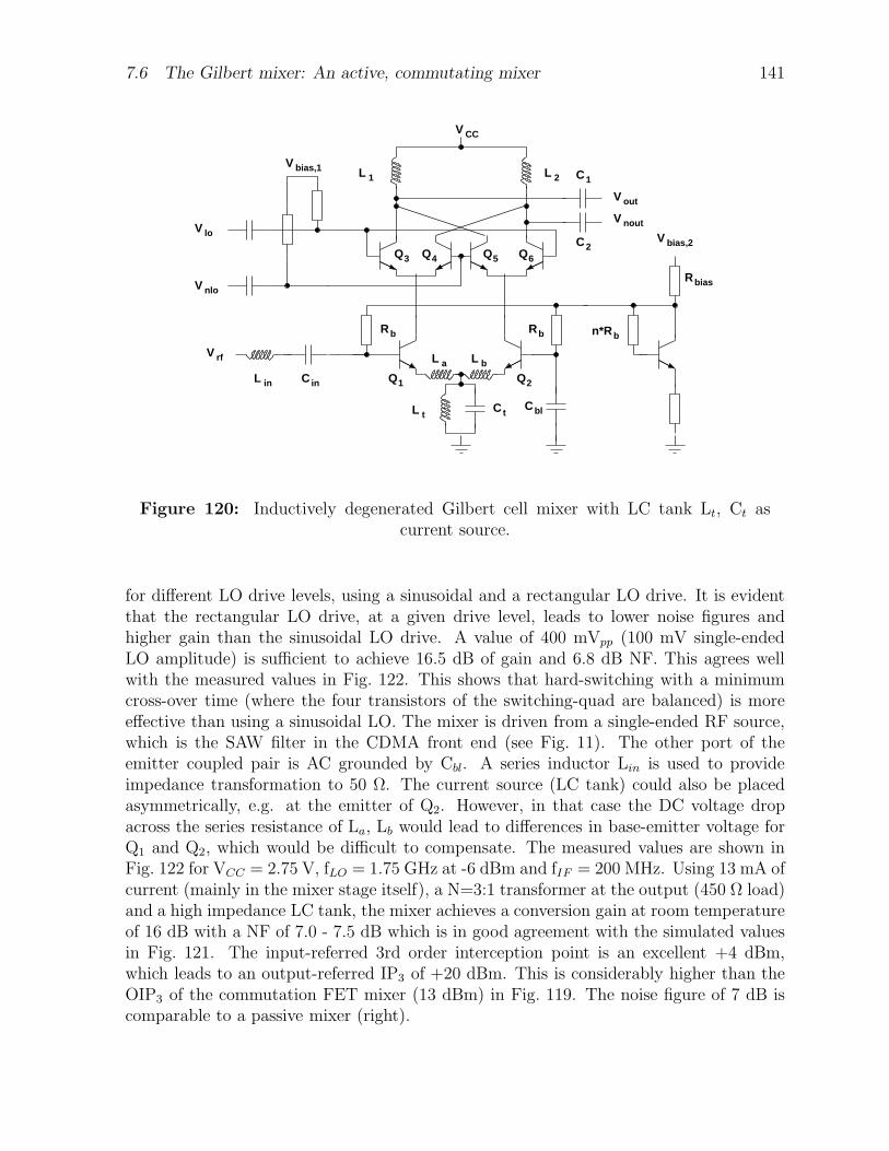
7.6 The Gilbert mixer: An active, commutating mixer 141
L t
V bias,2
L 2L 1
V CC
V lo
V nlo
V rf
C inL in
C t
Rbias
V bias,1
V out
V nout
C1
C2
Rb Rb
Cbl
L a L b
Q2Q1
Q3 Q4 Q5 Q6
n*R b
Figure 120: Inductively degenerated Gilbert cell mixer with LC tank Lt, Ct ascurrent source.
for different LO drive levels, using a sinusoidal and a rectangular LO drive. It is evidentthat the rectangular LO drive, at a given drive level, leads to lower noise figures andhigher gain than the sinusoidal LO drive. A value of 400 mVpp (100 mV single-endedLO amplitude) is sufficient to achieve 16.5 dB of gain and 6.8 dB NF. This agrees wellwith the measured values in Fig. 122. This shows that hard-switching with a minimumcross-over time (where the four transistors of the switching-quad are balanced) is moreeffective than using a sinusoidal LO. The mixer is driven from a single-ended RF source,which is the SAW filter in the CDMA front end (see Fig. 11). The other port of theemitter coupled pair is AC grounded by Cbl. A series inductor Lin is used to provideimpedance transformation to 50 Ω. The current source (LC tank) could also be placedasymmetrically, e.g. at the emitter of Q2. However, in that case the DC voltage dropacross the series resistance of La, Lb would lead to differences in base-emitter voltage forQ1 and Q2, which would be difficult to compensate. The measured values are shown inFig. 122 for VCC = 2.75 V, fLO = 1.75 GHz at -6 dBm and fIF = 200 MHz. Using 13 mA ofcurrent (mainly in the mixer stage itself), a N=3:1 transformer at the output (450 Ω load)and a high impedance LC tank, the mixer achieves a conversion gain at room temperatureof 16 dB with a NF of 7.0 - 7.5 dB which is in good agreement with the simulated valuesin Fig. 121. The input-referred 3rd order interception point is an excellent +4 dBm,which leads to an output-referred IP3 of +20 dBm. This is considerably higher than theOIP3 of the commutation FET mixer (13 dBm) in Fig. 119. The noise figure of 7 dB iscomparable to a passive mixer (right).
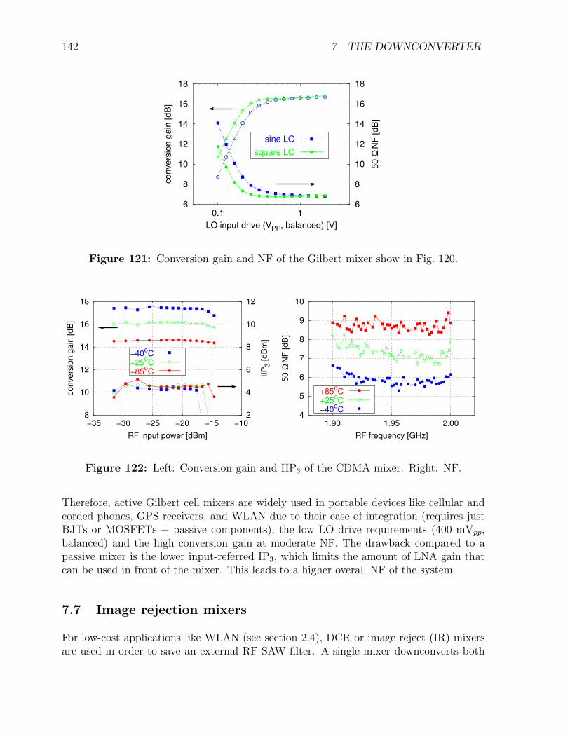
142 7 THE DOWNCONVERTER
6
8
10
12
14
16
18
0.1 16
8
10
12
14
16
18
convers
ion g
ain
[dB
]
50 Ω
NF
[dB
]
LO input drive (VPP, balanced) [V]
sine LO
square LO
Figure 121: Conversion gain and NF of the Gilbert mixer show in Fig. 120.
8
10
12
14
16
18
−35 −30 −25 −20 −15 −102
4
6
8
10
12
convers
ion g
ain
[dB
]
IIP
3 [dB
m]
RF input power [dBm]
−40oC
+25oC
+85oC
4
5
6
7
8
9
10
1.90 1.95 2.00
50 Ω
NF
[dB
]
RF frequency [GHz]
+85oC
+25oC
−40oC
Figure 122: Left: Conversion gain and IIP3 of the CDMA mixer. Right: NF.
Therefore, active Gilbert cell mixers are widely used in portable devices like cellular andcorded phones, GPS receivers, and WLAN due to their ease of integration (requires justBJTs or MOSFETs + passive components), the low LO drive requirements (400 mVpp,balanced) and the high conversion gain at moderate NF. The drawback compared to apassive mixer is the lower input-referred IP3, which limits the amount of LNA gain thatcan be used in front of the mixer. This leads to a higher overall NF of the system.
7.7 Image rejection mixers
For low-cost applications like WLAN (see section 2.4), DCR or image reject (IR) mixersare used in order to save an external RF SAW filter. A single mixer downconverts both
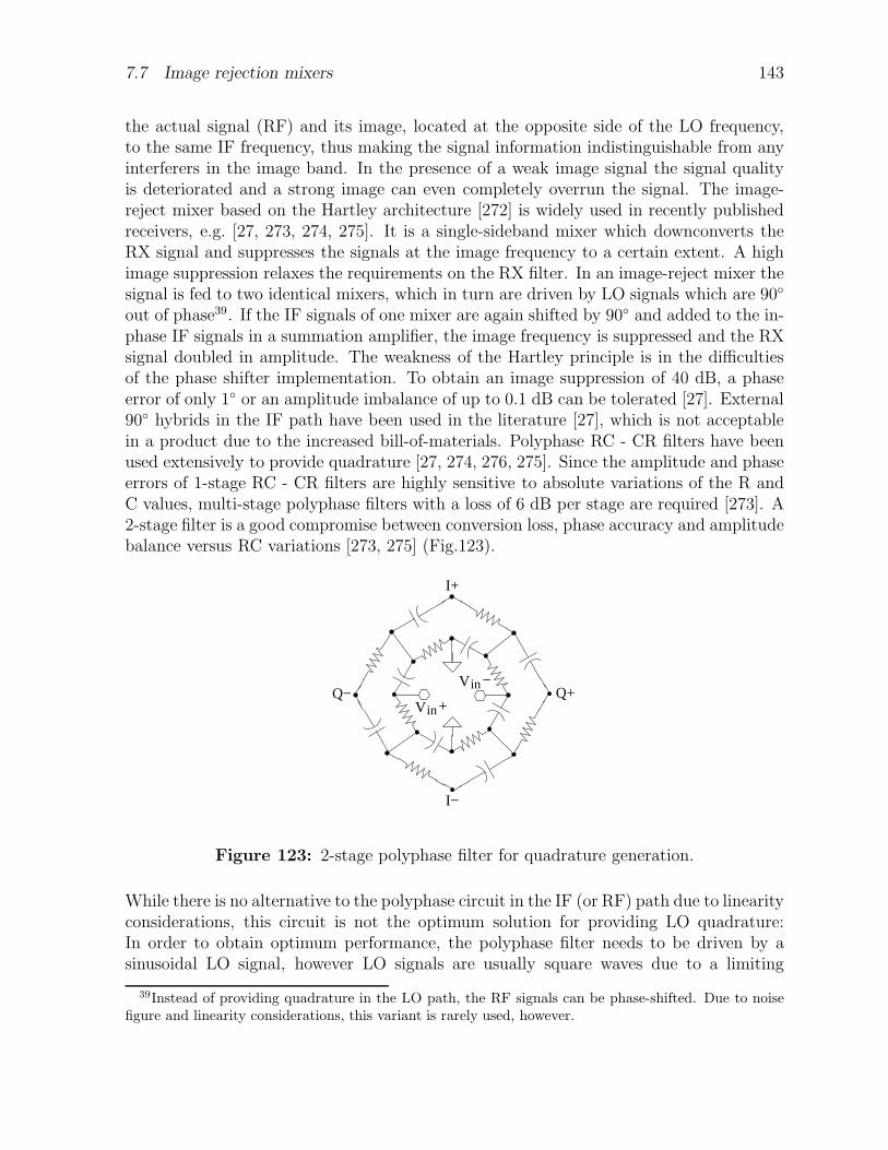
7.7 Image rejection mixers 143
the actual signal (RF) and its image, located at the opposite side of the LO frequency,to the same IF frequency, thus making the signal information indistinguishable from anyinterferers in the image band. In the presence of a weak image signal the signal qualityis deteriorated and a strong image can even completely overrun the signal. The image-reject mixer based on the Hartley architecture [272] is widely used in recently publishedreceivers, e.g. [27, 273, 274, 275]. It is a single-sideband mixer which downconverts theRX signal and suppresses the signals at the image frequency to a certain extent. A highimage suppression relaxes the requirements on the RX filter. In an image-reject mixer thesignal is fed to two identical mixers, which in turn are driven by LO signals which are 90
out of phase39. If the IF signals of one mixer are again shifted by 90 and added to the in-phase IF signals in a summation amplifier, the image frequency is suppressed and the RXsignal doubled in amplitude. The weakness of the Hartley principle is in the difficultiesof the phase shifter implementation. To obtain an image suppression of 40 dB, a phaseerror of only 1 or an amplitude imbalance of up to 0.1 dB can be tolerated [27]. External90 hybrids in the IF path have been used in the literature [27], which is not acceptablein a product due to the increased bill-of-materials. Polyphase RC - CR filters have beenused extensively to provide quadrature [27, 274, 276, 275]. Since the amplitude and phaseerrors of 1-stage RC - CR filters are highly sensitive to absolute variations of the R andC values, multi-stage polyphase filters with a loss of 6 dB per stage are required [273]. A2-stage filter is a good compromise between conversion loss, phase accuracy and amplitudebalance versus RC variations [273, 275] (Fig.123).
Vin +
Vin −
I+
Q− Q+
I−
Figure 123: 2-stage polyphase filter for quadrature generation.
While there is no alternative to the polyphase circuit in the IF (or RF) path due to linearityconsiderations, this circuit is not the optimum solution for providing LO quadrature:In order to obtain optimum performance, the polyphase filter needs to be driven by asinusoidal LO signal, however LO signals are usually square waves due to a limiting
39Instead of providing quadrature in the LO path, the RF signals can be phase-shifted. Due to noisefigure and linearity considerations, this variant is rarely used, however.
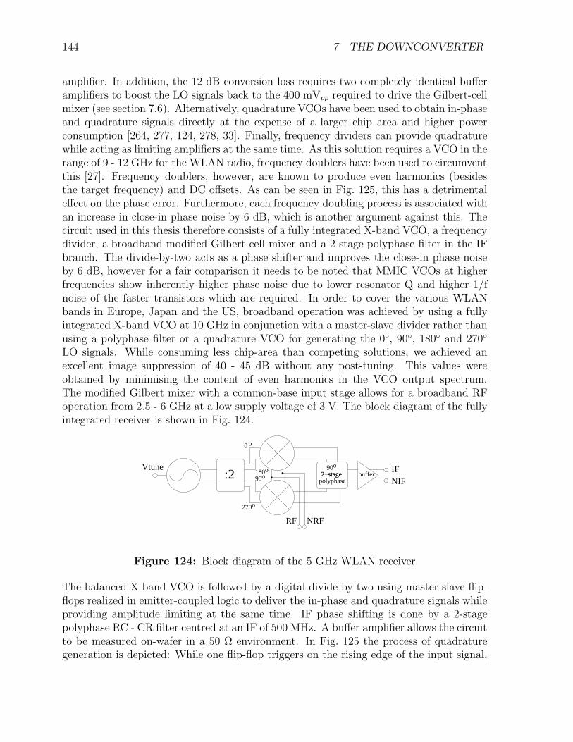
144 7 THE DOWNCONVERTER
amplifier. In addition, the 12 dB conversion loss requires two completely identical bufferamplifiers to boost the LO signals back to the 400 mVpp required to drive the Gilbert-cellmixer (see section 7.6). Alternatively, quadrature VCOs have been used to obtain in-phaseand quadrature signals directly at the expense of a larger chip area and higher powerconsumption [264, 277, 124, 278, 33]. Finally, frequency dividers can provide quadraturewhile acting as limiting amplifiers at the same time. As this solution requires a VCO in therange of 9 - 12 GHz for the WLAN radio, frequency doublers have been used to circumventthis [27]. Frequency doublers, however, are known to produce even harmonics (besidesthe target frequency) and DC offsets. As can be seen in Fig. 125, this has a detrimentaleffect on the phase error. Furthermore, each frequency doubling process is associated withan increase in close-in phase noise by 6 dB, which is another argument against this. Thecircuit used in this thesis therefore consists of a fully integrated X-band VCO, a frequencydivider, a broadband modified Gilbert-cell mixer and a 2-stage polyphase filter in the IFbranch. The divide-by-two acts as a phase shifter and improves the close-in phase noiseby 6 dB, however for a fair comparison it needs to be noted that MMIC VCOs at higherfrequencies show inherently higher phase noise due to lower resonator Q and higher 1/fnoise of the faster transistors which are required. In order to cover the various WLANbands in Europe, Japan and the US, broadband operation was achieved by using a fullyintegrated X-band VCO at 10 GHz in conjunction with a master-slave divider rather thanusing a polyphase filter or a quadrature VCO for generating the 0, 90, 180 and 270
LO signals. While consuming less chip-area than competing solutions, we achieved anexcellent image suppression of 40 - 45 dB without any post-tuning. This values wereobtained by minimising the content of even harmonics in the VCO output spectrum.The modified Gilbert mixer with a common-base input stage allows for a broadband RFoperation from 2.5 - 6 GHz at a low supply voltage of 3 V. The block diagram of the fullyintegrated receiver is shown in Fig. 124.
o90o90 o180
o270
:2
NRF
Vtune
RF
IFNIF
buffer2−stagepolyphase2−stage
0o
Figure 124: Block diagram of the 5 GHz WLAN receiver
The balanced X-band VCO is followed by a digital divide-by-two using master-slave flip-flops realized in emitter-coupled logic to deliver the in-phase and quadrature signals whileproviding amplitude limiting at the same time. IF phase shifting is done by a 2-stagepolyphase RC - CR filter centred at an IF of 500 MHz. A buffer amplifier allows the circuitto be measured on-wafer in a 50 Ω environment. In Fig. 125 the process of quadraturegeneration is depicted: While one flip-flop triggers on the rising edge of the input signal,
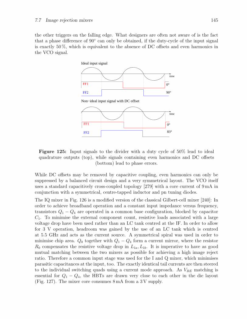
7.7 Image rejection mixers 145
the other triggers on the falling edge. What designers are often not aware of is the factthat a phase difference of 90 can only be obtained, if the duty-cycle of the input signalis exactly 50%, which is equivalent to the absence of DC offsets and even harmonics inthe VCO signal.
Non−ideal input signal with DC offset
time
0°
90°
time
0°
83°
FF2
FF2
FF1
Ideal input signal
FF1
Figure 125: Input signals to the divider with a duty cycle of 50% lead to idealquadrature outputs (top), while signals containing even harmonics and DC offsets
(bottom) lead to phase errors.
While DC offsets may be removed by capacitive coupling, even harmonics can only besuppressed by a balanced circuit design and a very symmetrical layout. The VCO itselfuses a standard capacitively cross-coupled topology [279] with a core current of 9mA inconjunction with a symmetrical, centre-tapped inductor and pn tuning diodes.
The IQ mixer in Fig. 126 is a modified version of the classical Gilbert-cell mixer [240]: Inorder to achieve broadband operation and a constant input impedance versus frequency,transistors Q1 − Q4 are operated in a common base configuration, blocked by capacitorC1. To minimise the external component count, resistive loads associated with a largevoltage drop have been used rather than an LC tank centred at the IF. In order to allowfor 3 V operation, headroom was gained by the use of an LC tank which is centredat 5.5 GHz and acts as the current source. A symmetrical spiral was used in order tominimise chip area. Q0 together with Q1 − Q4 form a current mirror, where the resistorR0 compensates the resistive voltage drop in L1a, L1b. It is imperative to have as goodmutual matching between the two mixers as possible for achieving a high image rejectratio. Therefore a common input stage was used for the I and Q mixer, which minimisesparasitic capacitances at the input, too. The exactly identical tail currents are then steeredto the individual switching quads using a current mode approach. As VBE matching isessential for Q1 − Q4, the HBTs are drawn very close to each other in the die layout(Fig. 127). The mixer core consumes 8mA from a 3V supply.
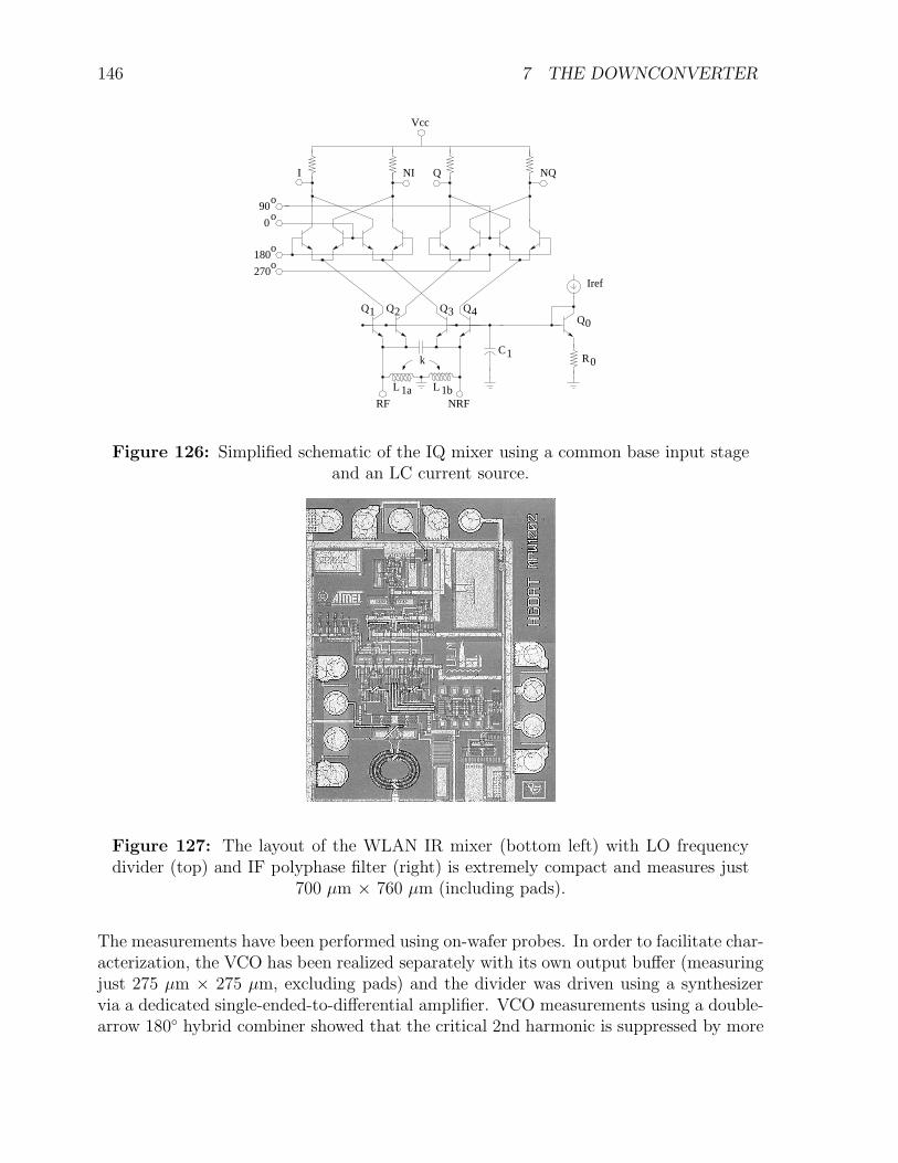
146 7 THE DOWNCONVERTER
1Q 3Q 4Q2Q
1aL 1bL
1C
0Q
0R
Iref
NI QI NQ
o
0o
90
180o
270o
Vcc
RF NRF
k
Figure 126: Simplified schematic of the IQ mixer using a common base input stageand an LC current source.
Figure 127: The layout of the WLAN IR mixer (bottom left) with LO frequencydivider (top) and IF polyphase filter (right) is extremely compact and measures just
700 µm × 760 µm (including pads).
The measurements have been performed using on-wafer probes. In order to facilitate char-acterization, the VCO has been realized separately with its own output buffer (measuringjust 275 µm × 275 µm, excluding pads) and the divider was driven using a synthesizervia a dedicated single-ended-to-differential amplifier. VCO measurements using a double-arrow 180 hybrid combiner showed that the critical 2nd harmonic is suppressed by more
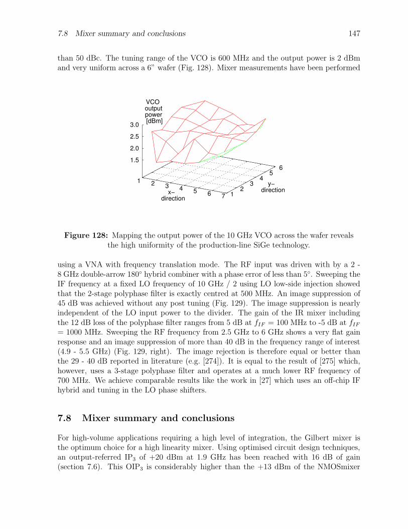
7.8 Mixer summary and conclusions 147
than 50 dBc. The tuning range of the VCO is 600 MHz and the output power is 2 dBmand very uniform across a 6” wafer (Fig. 128). Mixer measurements have been performed
1 2 3 4 5 6 7x−
direction1
23
45
6
y− direction
1.5
2.0
2.5
3.0
VCO output power [dBm]
Figure 128: Mapping the output power of the 10 GHz VCO across the wafer revealsthe high uniformity of the production-line SiGe technology.
using a VNA with frequency translation mode. The RF input was driven with by a 2 -8 GHz double-arrow 180 hybrid combiner with a phase error of less than 5. Sweeping theIF frequency at a fixed LO frequency of 10 GHz / 2 using LO low-side injection showedthat the 2-stage polyphase filter is exactly centred at 500 MHz. An image suppression of45 dB was achieved without any post tuning (Fig. 129). The image suppression is nearlyindependent of the LO input power to the divider. The gain of the IR mixer includingthe 12 dB loss of the polyphase filter ranges from 5 dB at fIF = 100 MHz to -5 dB at fIF
= 1000 MHz. Sweeping the RF frequency from 2.5 GHz to 6 GHz shows a very flat gainresponse and an image suppression of more than 40 dB in the frequency range of interest(4.9 - 5.5 GHz) (Fig. 129, right). The image rejection is therefore equal or better thanthe 29 - 40 dB reported in literature (e.g. [274]). It is equal to the result of [275] which,however, uses a 3-stage polyphase filter and operates at a much lower RF frequency of700 MHz. We achieve comparable results like the work in [27] which uses an off-chip IFhybrid and tuning in the LO phase shifters.
7.8 Mixer summary and conclusions
For high-volume applications requiring a high level of integration, the Gilbert mixer isthe optimum choice for a high linearity mixer. Using optimised circuit design techniques,an output-referred IP3 of +20 dBm at 1.9 GHz has been reached with 16 dB of gain(section 7.6). This OIP3 is considerably higher than the +13 dBm of the NMOSmixer
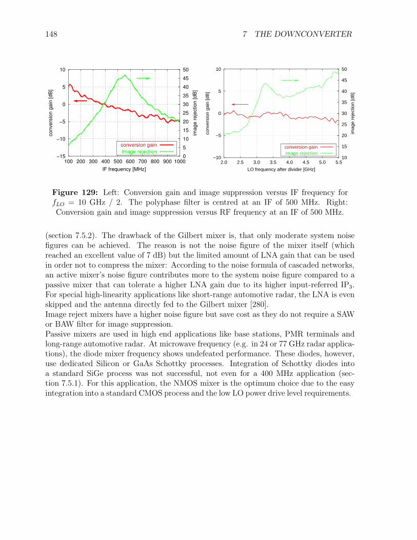
148 7 THE DOWNCONVERTER
−15
−10
−5
0
5
10
100 200 300 400 500 600 700 800 900 10000
5
10
15
20
25
30
35
40
45
50
convers
ion g
ain
[dB
]
image r
eje
ction [dB
]
IF frequency [MHz]
conversion gain
image rejection−10
−5
0
5
10
2.0 2.5 3.0 3.5 4.0 4.5 5.0 5.510
15
20
25
30
35
40
45
50
conv
ersi
on g
ain
[dB
]
imag
e re
ject
ion
[dB
]
LO frequency after divider [GHz]
conversion gainimage rejection
Figure 129: Left: Conversion gain and image suppression versus IF frequency forfLO = 10 GHz / 2. The polyphase filter is centred at an IF of 500 MHz. Right:Conversion gain and image suppression versus RF frequency at an IF of 500 MHz.
(section 7.5.2). The drawback of the Gilbert mixer is, that only moderate system noisefigures can be achieved. The reason is not the noise figure of the mixer itself (whichreached an excellent value of 7 dB) but the limited amount of LNA gain that can be usedin order not to compress the mixer: According to the noise formula of cascaded networks,an active mixer’s noise figure contributes more to the system noise figure compared to apassive mixer that can tolerate a higher LNA gain due to its higher input-referred IP3.For special high-linearity applications like short-range automotive radar, the LNA is evenskipped and the antenna directly fed to the Gilbert mixer [280].Image reject mixers have a higher noise figure but save cost as they do not require a SAWor BAW filter for image suppression.Passive mixers are used in high end applications like base stations, PMR terminals andlong-range automotive radar. At microwave frequency (e.g. in 24 or 77 GHz radar applica-tions), the diode mixer frequency shows undefeated performance. These diodes, however,use dedicated Silicon or GaAs Schottky processes. Integration of Schottky diodes intoa standard SiGe process was not successful, not even for a 400 MHz application (sec-tion 7.5.1). For this application, the NMOS mixer is the optimum choice due to the easyintegration into a standard CMOS process and the low LO power drive level requirements.
149
8 Conclusion
This thesis was carried out at the Competence Center for Integrated Circuits at UlmUniversity. It is a response to the high requirements in linearity of systems like UMTS,CDMA, GPS, TETRA and WLAN compared to its predecessors and arises from thedemands for higher data rates and higher cell capacities. Several development projectswithin the department targeted receive front-ends with high linearity. While the spec-ifications varied slightly, the need of new design techniques was common to all theseprojects. So rather than concentrating on one such system, this work reviews availablecircuit architectures and linearization techniques and chooses the methods best suited foreach problem. All circuits have been designed using production line Silicon-Germaniumbipolar and BiCMOS processes of Atmel Heilbronn (now TELEFUNKEN Semiconduc-tors [1]) and Atmel Colorado Springs.Theoretical considerations, extensive simulations and measurements showed that SiGeHBT technology – despite its exponential current-versus-voltage characteristics – offershigher linearity than pHEMT at low current consumption. For a given supply current, themost linear SiGe HBT LNA uses a single-stage cascode design with narrow band reactiveload and inductive series feedback. In order to achieve a high 3rd order intercept point(IP3) in the two-tone test, the difference frequency (often called ’beat frequency’) needsto be shorted properly. Different low-frequency termination techniques like broadbandsource termination, LC trap networks, inductive bias networks and active bias networksbased on operational amplifiers have been evaluated and the optimum solution was cho-sen, depending on the application. For very narrowband applications, cancellation ofintermodulation products by using capacitive parallel feedback can be exploited, leadingto high IP3. All realised LNAs have been benchmarked with published results and areclose to the theoretical optimum in linearity.Both passive mixers and active Gilbert cell mixers have been optimised with respect tolinearity. For systems where the interferers appear out-of-band of the SAW filter betweenLNA and mixer, an optimised Gilbert cell mixer is generally the best compromise insystem noise figure, linearity and power consumption. For systems with strong in-bandjammer (e.g. professional mobile radio terminals), a NMOS ring mixer with high peak-to-peak LO drive shows high input-referred linearity and allows for high LNA gain resultingin a very low system noise figure.Accurate models of passive on-chip components were critical for the success of this work,and therefore one chapter is dedicated to the characterization, simulation and modelingof planar structures on Silicon. Starting from investigations for repeatable on-wafer cal-ibrations and measurements, different 2.5D and 3D EM simulators have been evaluatedand it has been shown that a planar inductor on silicon is not a 2-dimensional electro-magnetic problem: Accurate simulation results for inductance and quality factor can onlybe obtained when taking into account current crowding effects between the metallisationlayers, modelling the current flow in their actual physical thickness. Choosing the correctinput parameters for the simulator is more important than selecting a special vendor’ssoftware. Different closed-form equations for inductance calculation have been evaluated
150 8 CONCLUSION
and good agreement has been found, even for ’historic’ work. By that, scaleable inductormodels, accurate in both inductance and quality factor, have been derived for the SiGe1,SiGe2-RF and SiGe2-Power design kits.For the future, highly integrated RF CMOS tranceivers will dominate all mass-market ap-plications, allowing for lower supply voltages (1.2 . . . 1.8 V instead of the 2.7 . . . 3.3 V usedin this thesis). SiGe HBT technology will find niche applications in front-end modulesand responds to this demand with higher device speeds (> 100 GHz) and lower parasiticcapacitances by improved isolation techniques, allowing for simple common emitter stagesinstead of cascode designs used in this thesis. This niche applications, however, will notenable sufficient volume for state-of-the art 8 inch SiGe HBT and SiGe BiCMOS waferfabs. Currently dominated by GaAs HBT and pHEMT technology, automotive radar at22 - 29 GHz and 77 - 81 GHz (for short-range applications) and 76 - 77 GHz (for long-rangeradars) will switch to SiGe HBT for cost and reliability reasons and higher integrationlevels [280, 281, 282, 283]. Thus, automotive radar will be the next killer application forSiGe HBT technology.
Frank J. Gruson, June 2010

151
Acknowledgement
At this point I would like to thank my supervisor Prof. Dr.-Ing. Hermann Schumacherfor his support and advice since October 2000. He handled many administrative taskssilently in the background, which allowed me to focus on my technical work. He wasalways there to discuss technical questions when necessary.I am grateful to Prof. Dr.-Ing. Joachim Burghartz, head of the Institute of Nano andMicroelectronic Systems at the University of Stuttgart, for serving as assessor and forreviewing this voluminous thesis in detail. Thank your for your advice and the excellentdiscussions we had.The team at the Competence Centre for Integrated Circuits at the Ulm University as-sisted me in many ways: I am especially grateful to Kai Boris Schad, Ertugrul Sonmezand Ferdinand Sigloch for their assistance in all computer and software related problems.Ursula Spitzberg assisted me in on-wafer RF measurements. Sven Hettich designed andpopulated most of the PCBs and he did a great job in supporting me within the SUPER-STAR project.The amount of people that supported me at Atmel in Heilbronn and Ulm barely fitsonto this page: I appreciate many excellent discussions with Dr. Gunther Bergmann,Dr. Udo Karthaus, Holger Schulz and Dr. Uwe Erben. The layout teams supportedmany of my designs and I would like to give my tanks to Jacqueline Luckert, IreneLogemann, Petra Bogel and Siggi Semmler in Ulm and Martin Averweg in Heilbronn.Dr. Andreas Schuppen, Harry Dietrich, Dietrich Zerrweck, Peter Brandl and Dr. JurgenBerntgen did a great job in running the SiGe wafers and provided me with an abundantamount of silicon (germanium), assisted by Dr. Wolfgang Schwerzel and Klaus Gratzkewho cared for wafer logistics – thanks ! It is impossible to count the number of ICs whichGerhard Kutscher and his team in Heilbronn and Dieter Griesinger in Ulm packagedfor me. Many thanks to Matthias Bopp and Winfried Rabe for managing the researchprojects.The cooperation with the Boston Design Center of TriQuint Semiconductors was a realpleasure for me. I enjoyed working with you guys and my special thanks go to XinweiWang and Wen Chen. I spent a wonderful summer in Boston in 2002 and I would like tothank Greg Henderson and Dilek Barlas and their families for that.To all those people whom I have not named explicitly or inadvertently left out, thankyou.This work would not have been possible without the full support of my family and I wouldlike to thank Heike for her continued support and encouragement. The understanding ofSarah and Theresa that their dad spent innumerable evenings, weekends and holidays forhis thesis was extremely helpful. Finally, I would like to thank my parents that enabledme to pursue my technical studies and always supported me.
Frank J. Gruson, June 2010
152 A NOISE FIGURE MEASUREMENTS
Method Suitable Advantage Disadvantageapplications
Gain Method Very high Easy setup, very accurate Limited by spectrumgain or at measuring very high NF, analyzer’s noise floor.
very high suitable for any frequency Cannot handle DUTsNF range with low gain & NF.
Y Factor Method Wide range Can measure wide range When measuring(using Spectrum of NF of NF at any frequency very high NF,
Analyser) regardless of gain error could be large.Y Factor Method Super low Convenient, very accurate Expensive equipment,
(using a Noise NF when measuring super low frequency rangeFigure Meter) NF (0 - 2 dB) limited
Table 24: Three methods of measuring noise figure [285].
A Noise figure measurements
A.1 General considerations
Although professional equipment for measuring noise figure is available since more than50 years, NF measurements are still tedious and the result is often frustrating and un-reproducible. J.C. Greene in his satirical article ”Noisemanship – The Art of MeasuringNoise Figures Nearly Independent of Device Performance” [284] already noted in 1961,that noise figure measurements can yield very high values (e.g. when measuring NF oncompetitor’s devices) or very low values (preferably when measuring your own devices).In today’s competitive environment where NF differences of less than 0.1 dB decide abouta design win, Greene’s conclusions are true now more than ever. The following appendixgives an overview about noise figure measurement techniques.For measuring noise figure, there exist at least three methods [285] which are depictedin table 24. All methods work for amplifiers, where input and output frequency are thesame, as well as for frequency translating devices like mixers. As the LO’s contributionto the noise figure is not removable by any kind of calibration, it is very important to usea generator of high spectral purity and low phase- and AM-noise (e.g. tube oscillator orquartz-oscillator) [286]. For poor LO-generators, a narrow-band filter yields a significantimprovement.
A.2 The Gain Method
Noise factor F and noise figure NF contain the important information about the noiseperformance of an RF system. The basic definition is [209]:
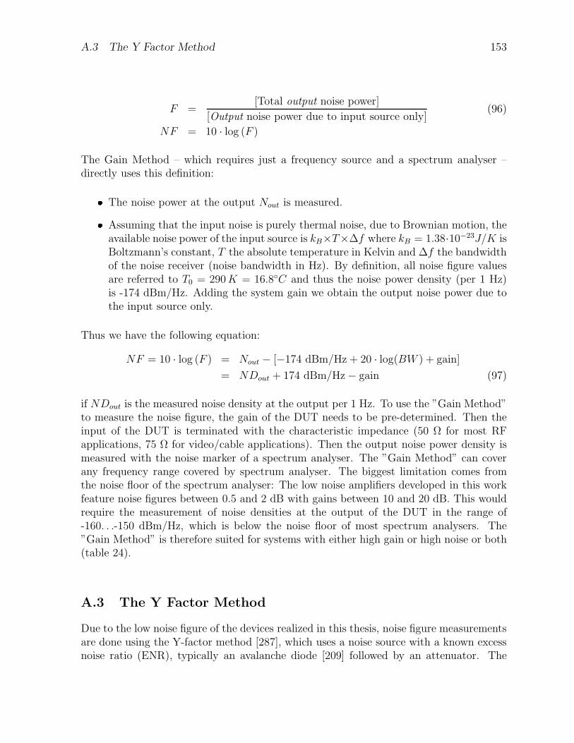
A.3 The Y Factor Method 153
F =[Total output noise power]
[Output noise power due to input source only](96)
NF = 10 · log (F )
The Gain Method – which requires just a frequency source and a spectrum analyser –directly uses this definition: The noise power at the output Nout is measured. Assuming that the input noise is purely thermal noise, due to Brownian motion, the
available noise power of the input source is kB×T×∆f where kB = 1.38·10−23J/K isBoltzmann’s constant, T the absolute temperature in Kelvin and ∆f the bandwidthof the noise receiver (noise bandwidth in Hz). By definition, all noise figure valuesare referred to T0 = 290 K = 16.8C and thus the noise power density (per 1 Hz)is -174 dBm/Hz. Adding the system gain we obtain the output noise power due tothe input source only.
Thus we have the following equation:
NF = 10 · log (F ) = Nout − [−174 dBm/Hz + 20 · log(BW ) + gain]
= NDout + 174 dBm/Hz − gain (97)
if NDout is the measured noise density at the output per 1 Hz. To use the ”Gain Method”to measure the noise figure, the gain of the DUT needs to be pre-determined. Then theinput of the DUT is terminated with the characteristic impedance (50 Ω for most RFapplications, 75 Ω for video/cable applications). Then the output noise power density ismeasured with the noise marker of a spectrum analyser. The ”Gain Method” can coverany frequency range covered by spectrum analyser. The biggest limitation comes fromthe noise floor of the spectrum analyser: The low noise amplifiers developed in this workfeature noise figures between 0.5 and 2 dB with gains between 10 and 20 dB. This wouldrequire the measurement of noise densities at the output of the DUT in the range of-160. . .-150 dBm/Hz, which is below the noise floor of most spectrum analysers. The”Gain Method” is therefore suited for systems with either high gain or high noise or both(table 24).
A.3 The Y Factor Method
Due to the low noise figure of the devices realized in this thesis, noise figure measurementsare done using the Y-factor method [287], which uses a noise source with a known excessnoise ratio (ENR), typically an avalanche diode [209] followed by an attenuator. The
154 A NOISE FIGURE MEASUREMENTS
ENR describes the difference in noise temperatures between ’hot’ (noise source ON) and’cold’ (noise source OFF) [287, 288, 289, 285].
ENR(dB) = 10 · log[Th − Tc
Tc
]
(98)
Using this technique, noise figure is measured by injecting an accurately known amplitudeof noise Th into the amplifier (DUT) and finally into a receiver (see Fig. 130). This iscompared with injecting ambient temperature noise Tc into the same setup.
Figure 130: Setup for RF noise measurements [290].
As the noise source in OFF state – due to the built-in attenuator – represents a pure 50 Ωresistor, ENR is easily converted to noise spectral by the following equation [289]
− 174 dBm/Hz = 0 dB ENR (99)
The ENR of the noise source is tabulated at spot frequency points throughout the specifiedfrequency range and is interpolated in between these frequency points. For the input noisetemperatures of Th and Tc, the measured output noise powers are referred to as Nh andNc, respectively. These two noise powers, when expressed as a ratio, represent the Y-factorvalue given by
YFact =Nh
Nc(100)
The noise figure is then calculated by [285]
NF(dB) = ENR(dB) − 10 · log (YFact − 1) (101)
In space applications, instead of NF often equivalent noise temperatures are given. Suchan equivalent input noise temperature Te can be assigned to the DUT via its (linear)noise factor F using the equation
F = 1 +Te
T0with NFdB = 10 · log(F ) (102)
A.3 The Y Factor Method 155
Automated equipment like the hp8970B noise figure meter or a spectrum analyser withnoise figure personality (see table 24) is available to record the Y-factor versus frequency,to calculate the gain as well as F, Te and NF and to perform the 2nd stage error correc-tion which corrects the measured noise temperature by the influence of the noise figureequipment [288].From Eqn. 101 it is evident that the accuracy of the noise figure measurement is only asgood as the accuracy of the calibrated ENR value of the noise source, specified by thesupplier with an error of ± 0.15 . . . ± 0.18 dB. The accuracy of the noise receiver formeasuring the ratio of the noise powers (Eqn. 100) can be as low as ± 0.05 dB [291, 292].Each noise figure measurement is therefore associated with an unavoidable measurementerror in the order of at least ± 0.2 dB, which is mainly due to the uncertainty of the ENRcalibration data [287]. If the measurement was not done properly, the measurement errorcan easily be higher. The following precautions are necessary: Spectrum analysers with noise figure personality may be used to measure noise
figures (see table 24, middle). While spectrum analysers are excellent devices tocover a power range of 80 dB with medium accuracy, they are not optimised tomeasure the ratio of two power levels with high accuracy. Agilent gives a total errorof 0.24 - 0.46 dB for its spectrum-analyser based NF measurement system (includingthe ENR impreciseness of the noise diode) [293]. Noise figure analysers (see table 24,bottom) like the hp8970B should be preferred over spectrum analysers, as they arelinearised and optimised for the limited power range of a noise figure measurement. The signals delivered by the noise source to the DUT are extremely small. Toprevent the DUT picking up interferers, the measurement environment needs to beshielded by a Faraday cage against radiation from fluorescent lamps, computer andmeasurement equipment, nearby basestations or TV and radio transmitters. Sweptmeasurements should be preferred over fixed frequency measurements in order toidentify such interferers.
One of the most important contributions to measurement accuracy is a good match (lowVSWR) between the noise source output and the device connected to it (DUT or testsetup) [290, 286], an error which becomes especially pronounced at noise figures below6 dB (Fig. 3 in [287]). During measurement, a small amount of noise power is reflectedat the DUT input (or at the test setup during calibration) (see Fig. 131).
Figure 131: Reflected power during noise figure measurements [290].
156 A NOISE FIGURE MEASUREMENTS
Some of this reflected power is reflected again at the noise source output with unpre-dictable phase, thus changing the measured power of the signal in an uncertain way. Thepreferred setup for noise figure measurements at RF frequencies is shown in Fig. 130.The isolator and preamplifier are added to reduce measurement uncertainty. An isolatorlike the one shown in Fig. 132 reduces reflected power between the DUT and the testsetup and makes sure that the noise figure meter sees exactly the same impedance duringcalibration (DUT removed) and NF measurement (DUT in place). This is vital whenremoving the influence of isolator, preamplifier and noise figure meter during the 2ndstage error correction. The preamplifier reduces the noise figure of the test setup. Thispreamplifier is often integrated into the noise figure meter, but in the case of the hp8970Bhas a noise figure of 6 - 9 dB. As isolators are inherently narrowband, for the widebandcase it is reported to replace the isolator with a low VSWR attenuator of approximately6 to 10 dB [286]. This was not done in our measurements, as the attenuator results in anincreased NF of the measurement system, and therefore increases the influence of the 2ndstage error correction. Instead, a low noise preamplifier with excellent wideband inputmatch S11 was designed (section A.4). The high reverse isolation of the device makes S11
insensitive against mismatch of the noise receiver (see figure 135).
−45
−40
−35
−30
−25
−20
−15
−10
−5
0
0.0 0.5 1.0 1.5 2.0 2.5 3.0 3.5 4.0
S21 a
nd S
12 [dB
], r
etu
rn loss S
11 [dB
]
frequency [GHz]
transmission S21
isolation S12
input return loss S11
Figure 132: Due to the high isolation, isolators provide excellent input match(>23 dB) independent of the output load, while attenuating the signal by as little as
0.3 dB (Ditom D3C0120 isolator, 1.7-2.0 GHz).
Noise sources are commonly available with nominal ENR values of 15 dB and 6 dB. In the15 dB source, the raw ENR of the GaAs avalanche diode of typically 25 dB is attenuatedby 10 dB, in the 6 dB source by approximately 20 dB [289]. The 6 dB source thereforeshows a return loss of at least 40 dB, independent from the noise diode being ’on’ or ’off’.This means that there is less difference in impedance between ’hot’ and ’cold ’ comparedto the 15 dB source. If the noise source changes impedance when turned on, the DUTsees a different excess noise than is calibrated for the noise source [290]. Therefore it is
A.4 Improving measurement accuracy by a low-noise preamplifier 157
Expected Noise Source Typical NF Typical GainNoise Figure [dB] Nominal ENR Uncertainty [dB] Uncertainty [dB]
0 to 10 5 ± 0.24 ± 0.8310 to 20 1020 to 35 15 ± 0.41 ± 0.83
Table 25: Rule of thumb for ENR versus expected noise figure of the DUT [289]and typical measurement uncertainties of a commercial measurement setup (10 MHz-
3 GHz) [293].
necessary to use a 5 - 6 dB ENR noise source when measuring noise figures up to about10 dB and particularly to minimise measurement uncertainties when the noise figure of the DUT is very low and the DUT is sensitive to changes
in source impedance (e.g. has a large equivalent noise resistance Rn).
The use of a source with low ENR has the following advantages: Errors due to non-linearities within the noise figure meter are reduced, if the dif-ference in noise power between hot and cold (Yfact) at the instrument is lower (notethat Yfact − 1 is always lower than the ENR, see equation 101). Many automatic noise figure analysers switch attenuators in order to handle highernoise power levels. This increases the NF of the measurement system and theinfluence of the 2nd stage error correction will be more pronounced. With a low ENRsource the instrument will use less attenuation, resulting in a lower instrument noisefigure. The influence of the 2nd stage error correction will be lower, which reducesmeasurement uncertainty (see table 25). Using a 15 dB noise source together with a10 dB pad instead of a 5 - 6 dB noise source is possible [286], but the uncertaintiesof ENR and pad attenuation sum up in this case.
A.4 Improving measurement accuracy by a low-noise preampli-fier
The disadvantage of noise diodes with low ENR is that the noise signal might be toolow for the noise figure meter, especially if the DUT has a low amplification (e.g. theTETRA/TETRAPOL LNA in low gain mode). In that case the noise figure meter cannotchoose the voltage swing to be in the optimum linearity range of its voltage detector as itneeds to switch its IF attenuators to the state with the lowest attenuation. To overcomethis problems, a broad band, low noise preamplifier for the hp8970B noise figure meterhas been designed under the following constraints:
158 A NOISE FIGURE MEASUREMENTS The gain should be flat across the frequency range of 0.3 - 3 GHz. A good input match is required to allow for broad band measurements without usingisolators or at frequencies where isolators are difficult to get (e.g. < 800 MHz) In order to make this input match independent from the match of the noise figuremeter, a high reverse isolation is required so that S21 · S12 1. This in turn leadsto a stable amplifier with high Rollett factor, which is a desirable side effect. The noise figure should be well below the noise figure of the hp8970B (6. . .9 dB) inorder to lower the cascaded noise figure considerably. No attempt was made to optimise the large signal behaviour (P1 dB and IIP3).
100 pF
0.4 nH
10 Ω
1000 Ω
16 pF
18 Ω39 Ω
10 mA 5 mA
RFin
RFout
3V LDO
MAX8870
> 3.5V
regulated 3V supply
10 nF
1 uF
100 pF
10 u
F //
10 n
F
100 pF 270 Ω
Figure 133: Broadband pre-amplifier for the hp8970B noise figure meter realizedusing e-PHEMTs.
State-of-the-art 0.15 µm enhancement-mode, pseudomorphic GaAs HEMTs (e-pHEMTs)available from Agilent Technologies with the type number ATF-551M4, housed in a thinminiature leadless package with low lead inductances were used in the design, as the lowinput capacitance of FETs allows for a broad-band design [294, 255, 87]. Resistive parallelfeedback was used in the first stage for achieving a good broadband input match. In ordernot to deteriorate the low NF of the e-pHEMTs too much (NFmin = 0.41 dB @ 2 GHz for10 mA and 2.7 V with 17.9 dB of associated gain), the feedback resistor was maximisedunder the S11 constraint, resulting in a value of 1 kΩ at a 270 Ω load. Inductive sourcedegeneration of 0.4 nH, realized as a short line on the 0.5 mm thick RO4003 substrate,
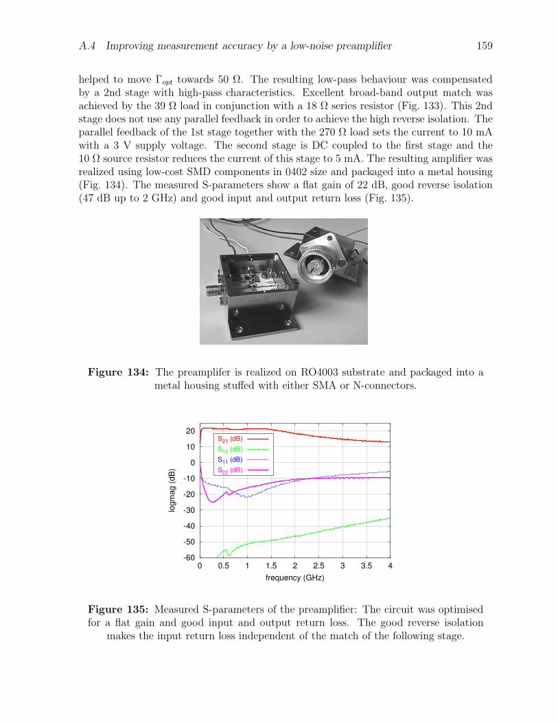
A.4 Improving measurement accuracy by a low-noise preamplifier 159
helped to move Γopt towards 50 Ω. The resulting low-pass behaviour was compensatedby a 2nd stage with high-pass characteristics. Excellent broad-band output match wasachieved by the 39 Ω load in conjunction with a 18 Ω series resistor (Fig. 133). This 2ndstage does not use any parallel feedback in order to achieve the high reverse isolation. Theparallel feedback of the 1st stage together with the 270 Ω load sets the current to 10 mAwith a 3 V supply voltage. The second stage is DC coupled to the first stage and the10 Ω source resistor reduces the current of this stage to 5 mA. The resulting amplifier wasrealized using low-cost SMD components in 0402 size and packaged into a metal housing(Fig. 134). The measured S-parameters show a flat gain of 22 dB, good reverse isolation(47 dB up to 2 GHz) and good input and output return loss (Fig. 135).
Figure 134: The preamplifer is realized on RO4003 substrate and packaged into ametal housing stuffed with either SMA or N-connectors.
-60
-50
-40
-30
-20
-10
0
10
20
0 0.5 1 1.5 2 2.5 3 3.5 4
logm
ag (
dB
)
frequency (GHz)
S21 (dB)
S12 (dB)
S11 (dB)
S22 (dB)
Figure 135: Measured S-parameters of the preamplifier: The circuit was optimisedfor a flat gain and good input and output return loss. The good reverse isolation
makes the input return loss independent of the match of the following stage.
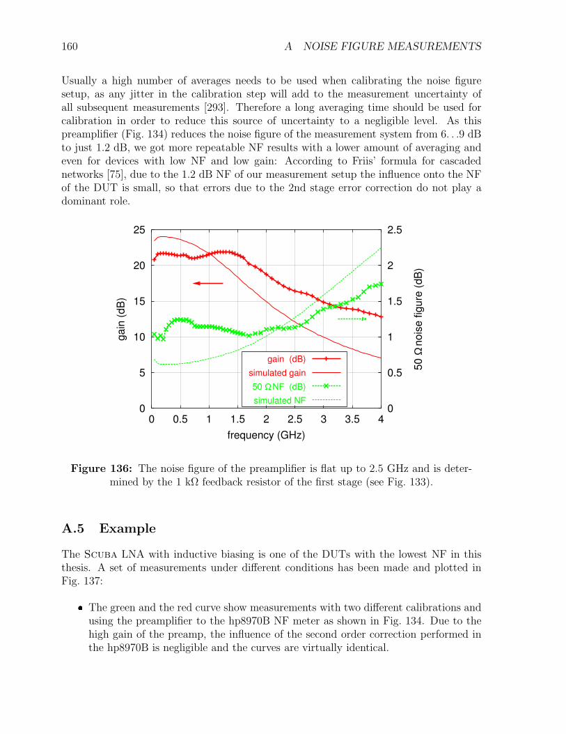
160 A NOISE FIGURE MEASUREMENTS
Usually a high number of averages needs to be used when calibrating the noise figuresetup, as any jitter in the calibration step will add to the measurement uncertainty ofall subsequent measurements [293]. Therefore a long averaging time should be used forcalibration in order to reduce this source of uncertainty to a negligible level. As thispreamplifier (Fig. 134) reduces the noise figure of the measurement system from 6. . .9 dBto just 1.2 dB, we got more repeatable NF results with a lower amount of averaging andeven for devices with low NF and low gain: According to Friis’ formula for cascadednetworks [75], due to the 1.2 dB NF of our measurement setup the influence onto the NFof the DUT is small, so that errors due to the 2nd stage error correction do not play adominant role.
0
5
10
15
20
25
0 0.5 1 1.5 2 2.5 3 3.5 40
0.5
1
1.5
2
2.5
ga
in (
dB
)
50
Ω n
ois
e f
igu
re (
dB
)
frequency (GHz)
gain (dB)
simulated gain
50 Ω NF (dB)
simulated NF
Figure 136: The noise figure of the preamplifier is flat up to 2.5 GHz and is deter-mined by the 1 kΩ feedback resistor of the first stage (see Fig. 133).
A.5 Example
The Scuba LNA with inductive biasing is one of the DUTs with the lowest NF in thisthesis. A set of measurements under different conditions has been made and plotted inFig. 137: The green and the red curve show measurements with two different calibrations and
using the preamplifier to the hp8970B NF meter as shown in Fig. 134. Due to thehigh gain of the preamp, the influence of the second order correction performed inthe hp8970B is negligible and the curves are virtually identical.
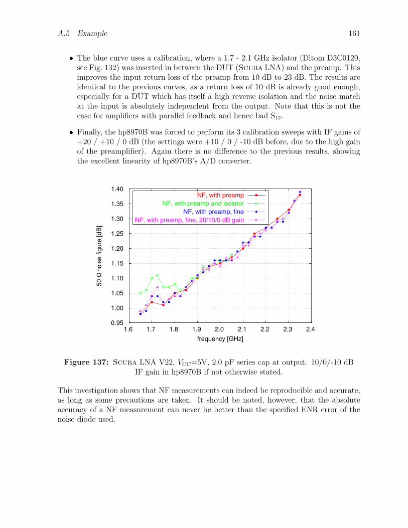
A.5 Example 161 The blue curve uses a calibration, where a 1.7 - 2.1 GHz isolator (Ditom D3C0120,see Fig. 132) was inserted in between the DUT (Scuba LNA) and the preamp. Thisimproves the input return loss of the preamp from 10 dB to 23 dB. The results areidentical to the previous curves, as a return loss of 10 dB is already good enough,especially for a DUT which has itself a high reverse isolation and the noise matchat the input is absolutely independent from the output. Note that this is not thecase for amplifiers with parallel feedback and hence bad S12. Finally, the hp8970B was forced to perform its 3 calibration sweeps with IF gains of+20 / +10 / 0 dB (the settings were +10 / 0 / -10 dB before, due to the high gainof the preamplifier). Again there is no difference to the previous results, showingthe excellent linearity of hp8970B’s A/D converter.
0.95
1.00
1.05
1.10
1.15
1.20
1.25
1.30
1.35
1.40
1.6 1.7 1.8 1.9 2.0 2.1 2.2 2.3 2.4
50
Ω n
ois
e f
igu
re [
dB
]
frequency [GHz]
NF, with preamp
NF, with preamp and isolator
NF, with preamp, fine
NF, with preamp, fine, 20/10/0 dB gain
Figure 137: Scuba LNA V22, VCC=5V, 2.0 pF series cap at output. 10/0/-10 dBIF gain in hp8970B if not otherwise stated.
This investigation shows that NF measurements can indeed be reproducible and accurate,as long as some precautions are taken. It should be noted, however, that the absoluteaccuracy of a NF measurement can never be better than the specified ENR error of thenoise diode used.
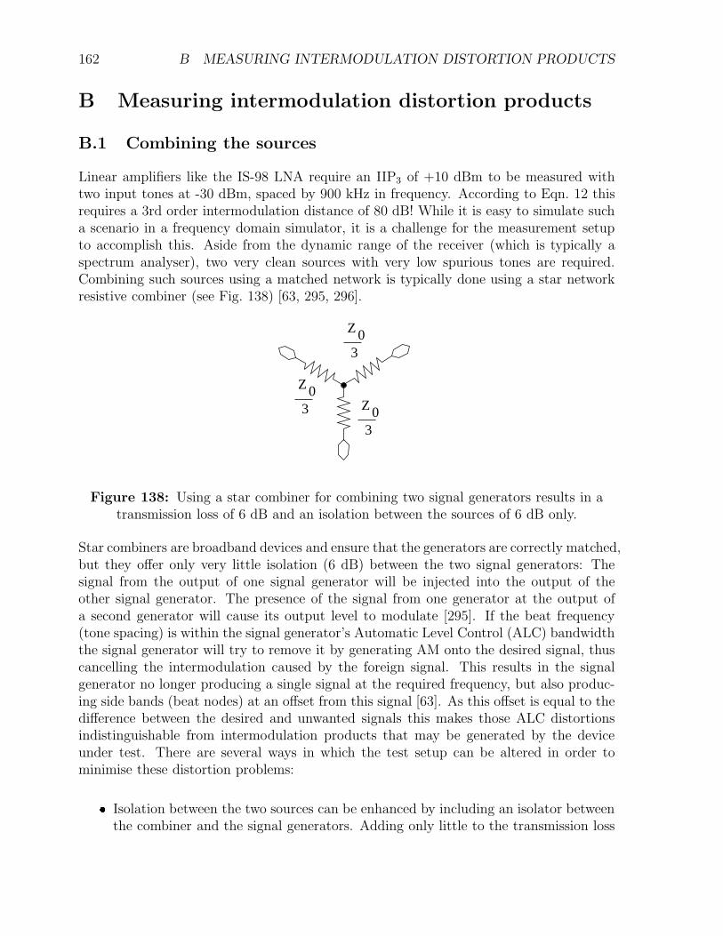
162 B MEASURING INTERMODULATION DISTORTION PRODUCTS
B Measuring intermodulation distortion products
B.1 Combining the sources
Linear amplifiers like the IS-98 LNA require an IIP3 of +10 dBm to be measured withtwo input tones at -30 dBm, spaced by 900 kHz in frequency. According to Eqn. 12 thisrequires a 3rd order intermodulation distance of 80 dB! While it is easy to simulate sucha scenario in a frequency domain simulator, it is a challenge for the measurement setupto accomplish this. Aside from the dynamic range of the receiver (which is typically aspectrum analyser), two very clean sources with very low spurious tones are required.Combining such sources using a matched network is typically done using a star networkresistive combiner (see Fig. 138) [63, 295, 296].
Z 03 Z 0
3
Z 03
Figure 138: Using a star combiner for combining two signal generators results in atransmission loss of 6 dB and an isolation between the sources of 6 dB only.
Star combiners are broadband devices and ensure that the generators are correctly matched,but they offer only very little isolation (6 dB) between the two signal generators: Thesignal from the output of one signal generator will be injected into the output of theother signal generator. The presence of the signal from one generator at the output ofa second generator will cause its output level to modulate [295]. If the beat frequency(tone spacing) is within the signal generator’s Automatic Level Control (ALC) bandwidththe signal generator will try to remove it by generating AM onto the desired signal, thuscancelling the intermodulation caused by the foreign signal. This results in the signalgenerator no longer producing a single signal at the required frequency, but also produc-ing side bands (beat nodes) at an offset from this signal [63]. As this offset is equal to thedifference between the desired and unwanted signals this makes those ALC distortionsindistinguishable from intermodulation products that may be generated by the deviceunder test. There are several ways in which the test setup can be altered in order tominimise these distortion problems: Isolation between the two sources can be enhanced by including an isolator between
the combiner and the signal generators. Adding only little to the transmission loss
B.2 Setting up the spectrum analyser 163
from the source to the combiner, it prevents signals being reflected back into thesources [63]. These devices, however, are inherently narrowband and under certainconditions they may generate their own intermodulation products. Reactive, hybrid combiners can be used in place of resistive combiners. The devicewhich was used in most of the measurements of this work was the ZESC-2-11 frommini-circuits [297] (see Fig. 139). Due to its broadband nature, it is assumed thatthis hybrid is based on transformers using ferrite cores similar to the 6 dB hybridspresented in [295]. Despite of being a low-cost part, it offers significant advantagesover the star network of Fig. 138. As ferrites themselves show intermodulation at high input drive level, for amplifierswith very high linearity they should be replaced by Wilkinson-type 3 dB splittersbased on air-core inductors [295] (for lower frequencies) or striplines (for higherfrequencies). The drawback of this devices is their limited bandwidth. For mixer testing, a low pass filter should be inserted between the combiner andthe device under test to reduce harmonic levels. Any harmonic distortion from themixer is indistinguishable from that of the generator [63, 295, 296].
B.2 Setting up the spectrum analyser
Spectrum analysers produce intermodulation products if operated incorrectly [63]. Whenchoosing a proper analyser, the intermodulation free dynamic range needs to be consid-ered. As a rule, spectrum analysers are designed to operate at their best with -30. . .-40 dBm at the analyser’s mixer input. This means that increasing the internal atten-uation needs to be considered. As the attenuation level is increased so the noise floorrises and potentially hides any intermodulation products. The measurement bandwidthmust therefore be reduced in order to reduce the noise floor [63]. As a quick check, if theintermodulation product displayed by the analyser is real, its level relative to the carrierwill not be affected by slightly varying the input attenuation of the spectrum analyser.When working with very low input levels, the input attenuation may be decreased. As themixer of the spectrum analyser typically is poorly matched, at least 6 dB of attenuationis required to provide sufficient return loss to the DUT. This is especially true for thenarrow-band LNAs developed in this work, as their IP3 is very sensitive with respect tochanges in the load.
B.3 Using a frequency translating vector network analyser
From October 2002, a vector network analyser with frequency translation mode was avail-able [298]. This allows to sweep the input frequency quickly over the frequency band, whilethe analyser records one of the fundamental output tones and one of the intermodulation
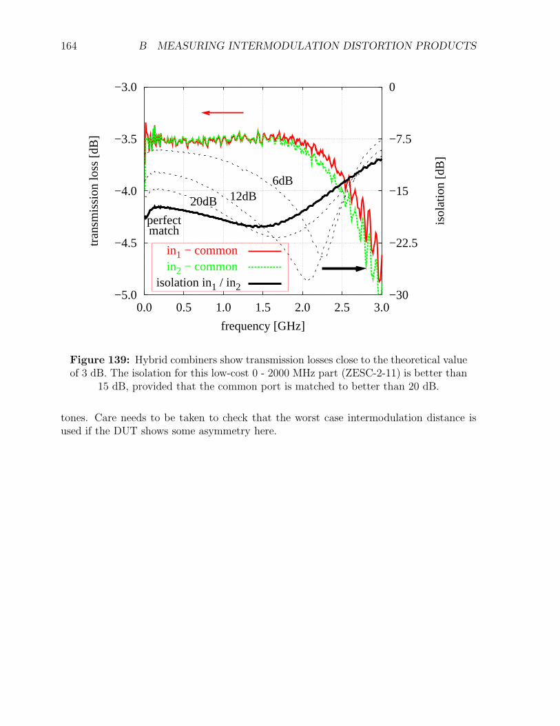
164 B MEASURING INTERMODULATION DISTORTION PRODUCTS
−5.0
−4.5
−4.0
−3.5
−3.0
0.0 0.5 1.0 1.5 2.0 2.5 3.0−30
−22.5
−15
−7.5
0tr
ansm
issi
on lo
ss [d
B]
isol
atio
n [d
B]
frequency [GHz]
perfectmatch
20dB 12dB6dB
in1 − common in2 − common
isolation in1 / in2
Figure 139: Hybrid combiners show transmission losses close to the theoretical valueof 3 dB. The isolation for this low-cost 0 - 2000 MHz part (ZESC-2-11) is better than
15 dB, provided that the common port is matched to better than 20 dB.
tones. Care needs to be taken to check that the worst case intermodulation distance isused if the DUT shows some asymmetry here.
165
C On-wafer characterisation of inductors -
the measurement challenge
C.1 Getting the right contact
When performing on-wafer measurements, the biggest problem initially was to get ade-quate contact on the aluminium pads. This pads form a thin layer of naturally, insulatingaluminium oxide as soon as they are exposed to the atmosphere. Depending on howmuch overtravel was used, the Picoprobe or Cascade air-coplanar probes slid on the pads,leading to arbitrary values for the series resistance and the Q-factor in turn. Whilethe standard wafer probes are made from an alloy of beryllium and copper to providegood electrical contact on gold pads, special probes existed with harder tungsten tips foraluminium pads. Despite of the considerable higher price of these probes, the problemremained the same, as tungsten also oxidises and the aluminium and aluminium oxideaccumulates on the probe tips after a few contacts, significantly increasing the contactresistance and hence resulting in poor measurement repeatability. Finally, the pads of nu-merous wafers were electroplated with a thin layer of nickel gold to allow for good contact.Now reproducible measurements were possible, leading to consistent results. In 2003, abreakthrough in probe tip technology occurred, when Cascade Microtech announced aseries of wafer probes called ’Infinity probes’ [299]. The revolutionary feature of thesetips was that rather than scratching away the oxide, they puncture it by using very sharptips (12× 12µm2) at the end of an otherwise blunt probe. This small size and the requiredsmall overtravel minimises the damage to the aluminium pad. Claiming a typical con-tact resistance below 0.05 Ω on aluminium pads, they also allow to reduce the diameterof the pads to below 40 µm, which reduces pad capacitance and hence the error whende-embedding the pads from the DUT (see section C.3). In addition, the construction ofthe coaxial-to-microstrip transition confines fringing fields more tightly than conventionalflexible coplanar tips. Better field confinement reduces unwanted coupling to nearby de-vices or other probe tips and thus allows to shrink the separation between individualdevices. As can be seen in Fig. 38, this new series of wafer probes, on non-plated pads,delivered nearly the same Q-factor as a conventional probe on gold plated pads.
C.2 Influence of the coaxial calibration technique
Using my simplified ’Thru’ de-embedding technique, which is described in section C.3, Icompared 4 different types of full 2-port on-wafer calibration procedures which all led toidentical values for the inductance, but varied in the results for the quality factor Q (seeFig. 140): SOLT-hp denotes the SOLT calibration procedure as built into Agilent’s hp8510C
vector network analyser. For the common SOLT (’Short’, ’Open’, ’Load’, ’Thru’)
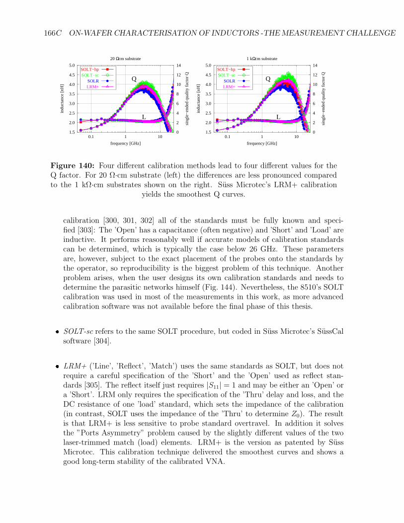
166C ON-WAFER CHARACTERISATION OF INDUCTORS -THE MEASUREMENT CHALLENGE
1.5
2.0
2.5
3.0
3.5
4.0
4.5
5.0
0.1 1 100
2
4
6
8
10
12
14in
duct
ance
[nH
]
sing
le−
ende
d qu
ality
fact
or Q
frequency [GHz]
20 Ωcm substrate
L
Q
SOLT−hpSOLT−sc
SOLRLRM+
1.5
2.0
2.5
3.0
3.5
4.0
4.5
5.0
0.1 1 100
2
4
6
8
10
12
14
indu
ctan
ce [
nH]
sing
le−
ende
d qu
ality
fact
or Q
frequency [GHz]
1 kΩcm substrate
L
Q
SOLT−hpSOLT−sc
SOLRLRM+
Figure 140: Four different calibration methods lead to four different values for theQ factor. For 20 Ω·cm substrate (left) the differences are less pronounced comparedto the 1 kΩ·cm substrates shown on the right. Suss Microtec’s LRM+ calibration
yields the smoothest Q curves.
calibration [300, 301, 302] all of the standards must be fully known and speci-fied [303]: The ’Open’ has a capacitance (often negative) and ’Short’ and ’Load’ areinductive. It performs reasonably well if accurate models of calibration standardscan be determined, which is typically the case below 26 GHz. These parametersare, however, subject to the exact placement of the probes onto the standards bythe operator, so reproducibility is the biggest problem of this technique. Anotherproblem arises, when the user designs its own calibration standards and needs todetermine the parasitic networks himself (Fig. 144). Nevertheless, the 8510’s SOLTcalibration was used in most of the measurements in this work, as more advancedcalibration software was not available before the final phase of this thesis. SOLT-sc refers to the same SOLT procedure, but coded in Suss Microtec’s SussCalsoftware [304]. LRM+ (’Line’, ’Reflect’, ’Match’) uses the same standards as SOLT, but does notrequire a careful specification of the ’Short’ and the ’Open’ used as reflect stan-dards [305]. The reflect itself just requires |S11| = 1 and may be either an ’Open’ ora ’Short’. LRM only requires the specification of the ’Thru’ delay and loss, and theDC resistance of one ’load’ standard, which sets the impedance of the calibration(in contrast, SOLT uses the impedance of the ’Thru’ to determine Z0). The resultis that LRM+ is less sensitive to probe standard overtravel. In addition it solvesthe ”Ports Asymmetry” problem caused by the slightly different values of the twolaser-trimmed match (load) elements. LRM+ is the version as patented by SussMicrotec. This calibration technique delivered the smoothest curves and shows agood long-term stability of the calibrated VNA.
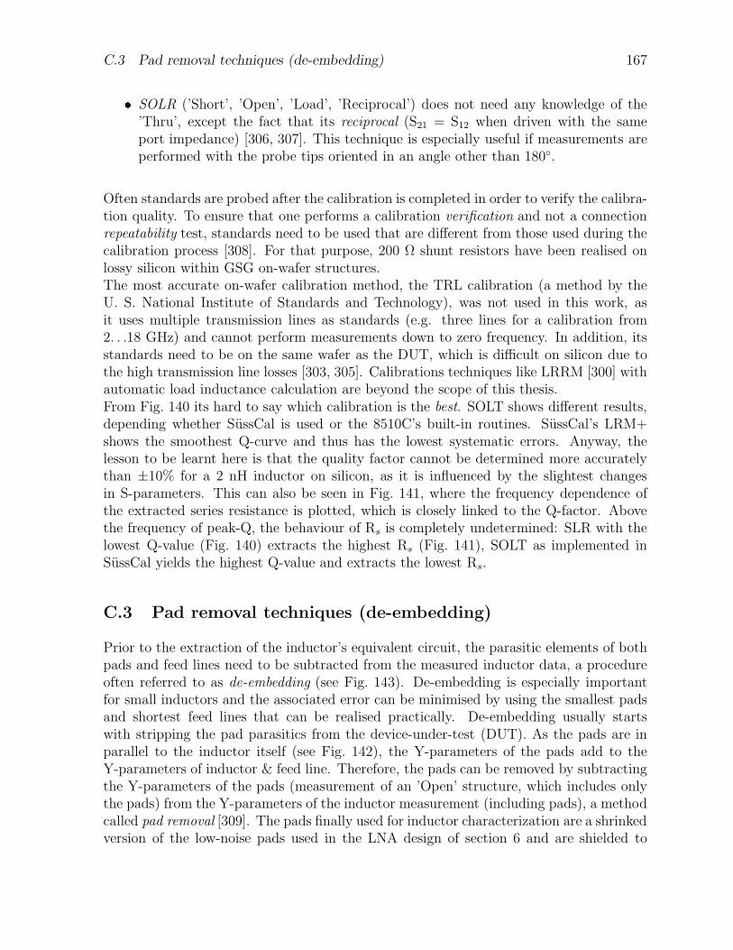
C.3 Pad removal techniques (de-embedding) 167 SOLR (’Short’, ’Open’, ’Load’, ’Reciprocal’) does not need any knowledge of the’Thru’, except the fact that its reciprocal (S21 = S12 when driven with the sameport impedance) [306, 307]. This technique is especially useful if measurements areperformed with the probe tips oriented in an angle other than 180.
Often standards are probed after the calibration is completed in order to verify the calibra-tion quality. To ensure that one performs a calibration verification and not a connectionrepeatability test, standards need to be used that are different from those used during thecalibration process [308]. For that purpose, 200 Ω shunt resistors have been realised onlossy silicon within GSG on-wafer structures.The most accurate on-wafer calibration method, the TRL calibration (a method by theU. S. National Institute of Standards and Technology), was not used in this work, asit uses multiple transmission lines as standards (e.g. three lines for a calibration from2. . .18 GHz) and cannot perform measurements down to zero frequency. In addition, itsstandards need to be on the same wafer as the DUT, which is difficult on silicon due tothe high transmission line losses [303, 305]. Calibrations techniques like LRRM [300] withautomatic load inductance calculation are beyond the scope of this thesis.From Fig. 140 its hard to say which calibration is the best. SOLT shows different results,depending whether SussCal is used or the 8510C’s built-in routines. SussCal’s LRM+shows the smoothest Q-curve and thus has the lowest systematic errors. Anyway, thelesson to be learnt here is that the quality factor cannot be determined more accuratelythan ±10% for a 2 nH inductor on silicon, as it is influenced by the slightest changesin S-parameters. This can also be seen in Fig. 141, where the frequency dependence ofthe extracted series resistance is plotted, which is closely linked to the Q-factor. Abovethe frequency of peak-Q, the behaviour of Rs is completely undetermined: SLR with thelowest Q-value (Fig. 140) extracts the highest Rs (Fig. 141), SOLT as implemented inSussCal yields the highest Q-value and extracts the lowest Rs.
C.3 Pad removal techniques (de-embedding)
Prior to the extraction of the inductor’s equivalent circuit, the parasitic elements of bothpads and feed lines need to be subtracted from the measured inductor data, a procedureoften referred to as de-embedding (see Fig. 143). De-embedding is especially importantfor small inductors and the associated error can be minimised by using the smallest padsand shortest feed lines that can be realised practically. De-embedding usually startswith stripping the pad parasitics from the device-under-test (DUT). As the pads are inparallel to the inductor itself (see Fig. 142), the Y-parameters of the pads add to theY-parameters of inductor & feed line. Therefore, the pads can be removed by subtractingthe Y-parameters of the pads (measurement of an ’Open’ structure, which includes onlythe pads) from the Y-parameters of the inductor measurement (including pads), a methodcalled pad removal [309]. The pads finally used for inductor characterization are a shrinkedversion of the low-noise pads used in the LNA design of section 6 and are shielded to
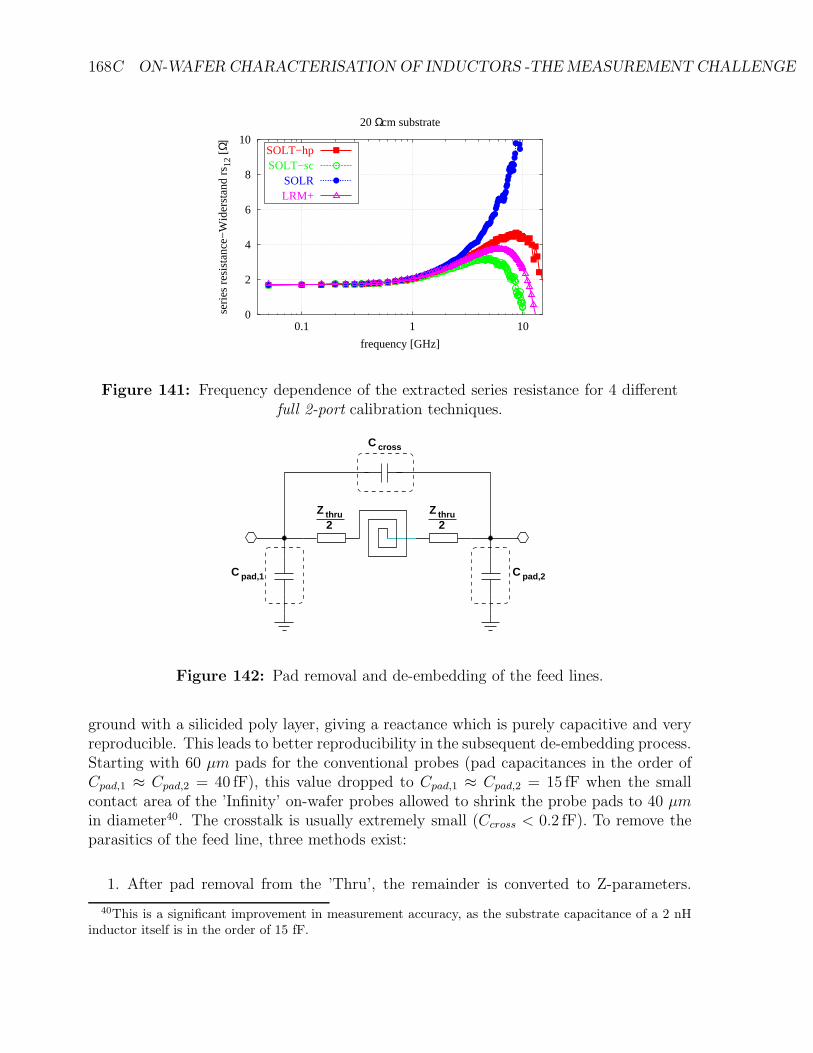
168C ON-WAFER CHARACTERISATION OF INDUCTORS -THE MEASUREMENT CHALLENGE
0
2
4
6
8
10
0.1 1 10
serie
s re
sist
ance
−W
ider
stan
d rs
12 [
Ω]
frequency [GHz]
20 Ωcm substrate
SOLT−hpSOLT−sc
SOLRLRM+
Figure 141: Frequency dependence of the extracted series resistance for 4 differentfull 2-port calibration techniques.
thruZ2
thruZ2
pad,1C
crossC
pad,2C
Figure 142: Pad removal and de-embedding of the feed lines.
ground with a silicided poly layer, giving a reactance which is purely capacitive and veryreproducible. This leads to better reproducibility in the subsequent de-embedding process.Starting with 60 µm pads for the conventional probes (pad capacitances in the order ofCpad,1 ≈ Cpad,2 = 40 fF), this value dropped to Cpad,1 ≈ Cpad,2 = 15 fF when the smallcontact area of the ’Infinity’ on-wafer probes allowed to shrink the probe pads to 40 µmin diameter40. The crosstalk is usually extremely small (Ccross < 0.2 fF). To remove theparasitics of the feed line, three methods exist:
1. After pad removal from the ’Thru’, the remainder is converted to Z-parameters.
40This is a significant improvement in measurement accuracy, as the substrate capacitance of a 2 nHinductor itself is in the order of 15 fF.
C.3 Pad removal techniques (de-embedding) 169
Zthru is extracted and the Z-parameters of the inductor are obtained by
Zind = Zind−open −Zthru
2×[
1 00 1
]
(103)
This method, however, assumes that the feed lines consist of inductance and seriesresistance only and have no shunt networks.
2. To overcome this limitation, I invented a 1-step de-embedding method which disas-sembles the S-parameters of the ’Thru’ into a π-network, where the shunt elementsare the sum of pad capacitances Cpad,1, Cpad,2 plus the shunt networks of the feedline itself. These shunt networks of pads and ’Thru’ are then stripped from theY-parameters of the DUT in 1 step. The feed resistance and inductance are thenremoved as in Eqn. 103. Note that this method requires just the knowledge of the’Thru’ S-parameters. No measurement of an ’Open’ is required.
3. The mathematically correct method starts after pad removal and expresses the feedline as a chain matrix [310, 311]:
v1 = v2 + Zthru · (−i2)i1 = (−i2)
(104)
The resulting A-matrix of the ’Thru’ is then
~~Athru =
[
1 Zthru
0 1
]
=
[
1 Zthru/20 1
]
×[
1 Zthru/20 1
]
=~~Athru/2 × ~~Athru/2 (105)
In practice, A12 is 6= 0 due to the shunt networks of the feed line41, but Eqn. 105remains approximately valid if A12 A21. The A-matrix of the inductor itself isthen obtained from the pad-removed A-matrix Aind−open according to
~~Aind =~~A
−1
thru/2 ×~~Aind−open × ~~A
−1
thru/2 (106)
Due to the complexity of the matrix inversion and multiplication, this method hasnot been implemented into our standard de-embedding software.
It is needless to say that the ’Thru’ structure needs to have exactly the same lengthlike the length of the feed lines of the inductors and needs to consist of the same metalcombination and width. It is convenient to lay out all inductors with the same length offeed lines, which requires just one ’Thru’. However, the author has seen many test arrays,where each inductor had its own ’Thru’ structure and each ’Thru’ structure was useless,as it had the same pad distance between port 1 and port 2 as the inductor and thus wasmuch too long. A inductor de-embedded with the three techniques is shown in Fig. 144.
41 It can be shown that A12 ≈ 2 · Y , where Y is the shunt conductance of the π network of the ’Thru’.
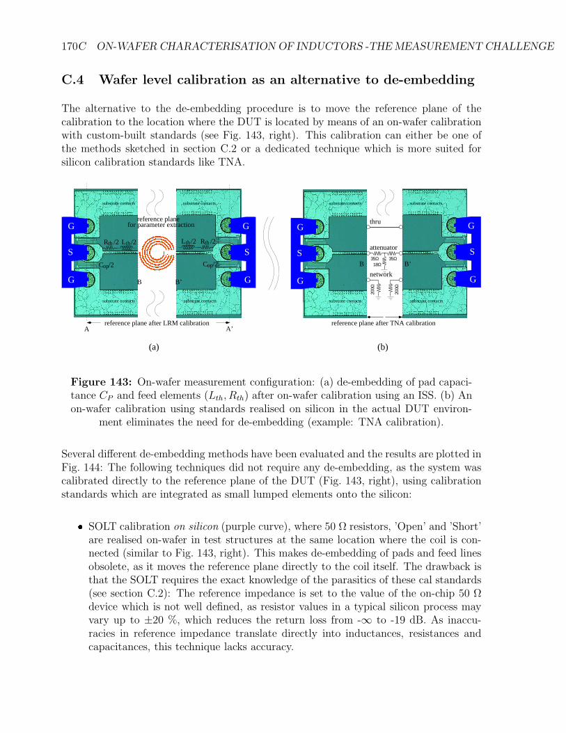
170C ON-WAFER CHARACTERISATION OF INDUCTORS -THE MEASUREMENT CHALLENGE
C.4 Wafer level calibration as an alternative to de-embedding
The alternative to the de-embedding procedure is to move the reference plane of thecalibration to the location where the DUT is located by means of an on-wafer calibrationwith custom-built standards (see Fig. 143, right). This calibration can either be one ofthe methods sketched in section C.2 or a dedicated technique which is more suited forsilicon calibration standards like TNA.
S
G
G
G
G
SS
G
G
C /2op
G
G
SC /2op
L /2th R /2thL /2thR /2th
substrate contacts
substrate contacts
substrate contacts
substrate contacts
reference plane after TNA calibration
(a) (b)
reference plane after LRM calibrationA’A
substrate contacts
substrate contacts
substrate contacts
substrate contacts
B B’
200Ω
200Ω
18Ω
attenuator
network
thru
35Ω35Ω
B’B
reference planefor parameter extraction
Figure 143: On-wafer measurement configuration: (a) de-embedding of pad capaci-tance CP and feed elements (Lth, Rth) after on-wafer calibration using an ISS. (b) Anon-wafer calibration using standards realised on silicon in the actual DUT environ-
ment eliminates the need for de-embedding (example: TNA calibration).
Several different de-embedding methods have been evaluated and the results are plotted inFig. 144: The following techniques did not require any de-embedding, as the system wascalibrated directly to the reference plane of the DUT (Fig. 143, right), using calibrationstandards which are integrated as small lumped elements onto the silicon: SOLT calibration on silicon (purple curve), where 50 Ω resistors, ’Open’ and ’Short’
are realised on-wafer in test structures at the same location where the coil is con-nected (similar to Fig. 143, right). This makes de-embedding of pads and feed linesobsolete, as it moves the reference plane directly to the coil itself. The drawback isthat the SOLT requires the exact knowledge of the parasitics of these cal standards(see section C.2): The reference impedance is set to the value of the on-chip 50 Ωdevice which is not well defined, as resistor values in a typical silicon process mayvary up to ±20 %, which reduces the return loss from -∞ to -19 dB. As inaccu-racies in reference impedance translate directly into inductances, resistances andcapacitances, this technique lacks accuracy.
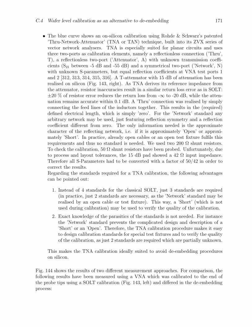
C.4 Wafer level calibration as an alternative to de-embedding 171 The blue curve shows an on-silicon calibration using Rohde & Schwarz’s patented’Thru-Network-Attenuator’ (TNA or TAN) technique, built into its ZVX series ofvector network analysers. TNA is especially suited for planar circuits and usesthree two-ports as calibration elements, namely a reflectionless connection (’Thru’,T), a reflectionless two-port (’Attenuator’, A) with unknown transmission coeffi-cients (S21 between -5 dB and -55 dB) and a symmetrical two-port (’Network’, N)with unknown S-parameters, but equal reflection coefficients at VNA test ports 1and 2 [312, 313, 314, 315, 316]. A T-attenuator with 15 dB of attenuation has beenrealised on silicon (Fig. 143, right). As TNA derives its reference impedance fromthe attenuator, resistor inaccuracies result in a similar return loss error as in SOLT:±20 % of resistor error reduces the return loss from -∞ to -20 dB, while the atten-uation remains accurate within 0.1 dB. A ’Thru’ connection was realised by simplyconnecting the feed lines of the inductors together. This results in the (required)defined electrical length, which is simply ’zero’. For the ’Network’ standard anyarbitrary network may be used, just featuring reflection symmetry and a reflectioncoefficient different from zero. The only information needed is the approximatecharacter of the reflecting network, i.e. if it is approximately ’Open’ or approxi-mately ’Short’. In practice, already open cables or an open test fixture fulfils thisrequirements and thus no standard is needed. We used two 200 Ω shunt resistors.To check the calibration, 50 Ω shunt resistors have been probed. Unfortunately, dueto process and layout tolerances, the 15 dB pad showed a 42 Ω input impedance.Therefore all S-Parameters had to be converted with a factor of 50/42 in order tocorrect the results.Regarding the standards required for a TNA calibration, the following advantagescan be pointed out:
1. Instead of 4 standards for the classical SOLT, just 3 standards are required(in practice, just 2 standards are necessary, as the ’Network’ standard may berealised by an open cable or test fixture). This way, a ’Short’ (which is notused during calibration) may be used to verify the quality of the calibration.
2. Exact knowledge of the parasitics of the standards is not needed. For instancethe ’Network’ standard prevents the complicated design and description of a’Short’ or an ’Open’. Therefore, the TNA calibration procedure makes it easyto design calibration standards for special test fixtures and to verify the qualityof the calibration, as just 2 standards are required which are partially unknown.
This makes the TNA calibration ideally suited to avoid de-embedding procedureson silicon.
Fig. 144 shows the results of two different measurement approaches. For comparison, thefollowing results have been measured using a VNA which was calibrated to the end ofthe probe tips using a SOLT calibration (Fig. 143, left) and differed in the de-embeddingprocess:
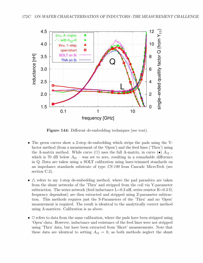
172C ON-WAFER CHARACTERISATION OF INDUCTORS -THE MEASUREMENT CHALLENGE
1.5
2.0
2.5
3.0
3.5
4.0
4.5
0.1 1 100
2
4
6
8
10
12in
du
cta
nce
[n
H]
sin
gle
−e
nd
ed
qu
altity f
acto
r Q
(fr
om
Y11)
frequency [GHz]
L
Q
thru, A−matrix
−’’− with A12=0
thru, 1−step
open/short
SOLT on Si
TNA on Si
Figure 144: Different de-embedding techniques (see text). The green curves show a 2-step de-embedding which strips the pads using the Y-factor method (from a measurement of the ’Open’) and the feed lines (’Thru’) usingthe A-matrix method. While curve (2) uses the full A-matrix, in curve (•) A12 –which is 70 dB below A21 – was set to zero, resulting in a remarkable differencein Q. Data are taken using a SOLT calibration using laser-trimmed standards onan impedance standards substrate of type CS-190 from Cascade MicroTech (seesection C.2). 4 refers to my 1-step de-embedding method, where the pad parasitics are takenfrom the shunt networks of the ’Thru’ and stripped from the coil via Y-parametersubtraction. The series network (feed inductance L=0.3 nH, series resistor R=0.3 Ω,frequency dependent) are then extracted and stripped using Z-parameter subtrac-tion. This methods requires just the S-Parameters of the ’Thru’ and no ’Open’measurement is required. The result is identical to the analytically correct methodusing A-matrices. Calibration is as above. 2 refers to data from the same calibration, where the pads have been stripped using’Open’-data. However, inductance and resistance of the feed lines were not strippedusing ’Thru’ data, but have been extracted from ’Short’ measurements. Note thatthese data are identical to setting A12 = 0, as both methods neglect the shunt
C.5 Choosing the right technique 173
capacitance of the feed line (not visible in a ’Short’ measurement due to the lowimpedance).
C.5 Choosing the right technique
Section C.2 compared different VNA error correction techniques, all using a calibrationreferenced to the probe tips based on a ceramic ISS. Using such a calibration, in sec-tion C.3 the reference plane has been shifted to the DUT by using different de-embeddingtechniques for pad-removal and feed line stripping. I found that a LRM+ calibration onan ISS, followed by a simplified 1-step de-embedding using just a ’Thru’ measurement iseasier to use and more consistent compared to a two-step method where first the pad-capacitances are extracted from an ’Open’ measurement and in a 2nd step inductanceand resistance of the feed lines from a ’Short’ or ’Thru’. This 1-step ’Thru’ de-embeddingtechnique resulted in virtually the same results for inductance and quality factor likethe mathematically correct treatment using the full transfer (A) matrix and needs onlyone de-embedding structure (a ’Thru’ with exactly the same length as the feed lines ofthe inductor). The often used 2-step ’Open/Short’ method resulted in substantial dif-ferences, as it neglects the shunt parasitics of the feed lines and thus attributes them tothe inductor itself, leading to a Q-factor being too small. The same error is introducedby using the technique based on a transfer matrix with A12 = 0. More complex threestep de-embedding techniques have been described recently [317], but we believe that our1-step ’Thru’ de-embedding technique is sufficiently accurate and at the same time easyto use. Section C.4 compared ISS- and de-embedding-based approaches to 2 wafer-levelcalibration techniques, which make de-embedding obsolete and avoid the errors being in-troduced by it. Compared to a SOLT wafer-level calibration, TNA is simple to use butstill suffers from generating an accurate reference impedance using commercially availablesilicon processes and would require laser trimming for the resistors.
C.6 On-wafer characterisation of 3-ports
In section 5.17, symmetrical inductors have been optimised and models have been gen-erated from EM simulated or measured 3-port S-parameters. To get 3-port inductorsby on-wafer measurements using a 2-port S-parameter test-set like the hp8510C, threeapproaches can be used:
1. The balanced inductance and Q-factor can simply be obtained by connecting to port1 and 2 and letting the 3rd port (ct) open. In this case, however, it is not possibleto extract the 3 substrate networks and the coupling factor k.
2. Each symmetrical inductor can be laid out 3 times:(i) port 1 is terminated with an on-chip 50 Ω resistor and port 2 and port 3 arerouted to on-wafer probes.
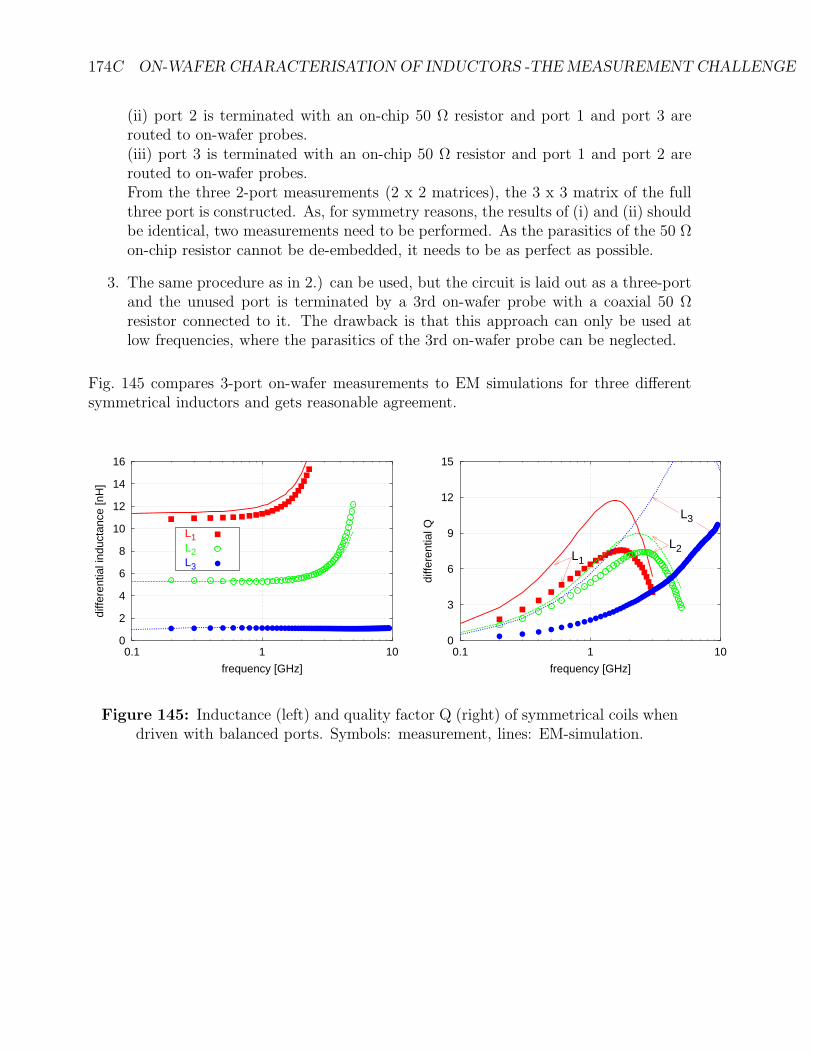
174C ON-WAFER CHARACTERISATION OF INDUCTORS -THE MEASUREMENT CHALLENGE
(ii) port 2 is terminated with an on-chip 50 Ω resistor and port 1 and port 3 arerouted to on-wafer probes.(iii) port 3 is terminated with an on-chip 50 Ω resistor and port 1 and port 2 arerouted to on-wafer probes.From the three 2-port measurements (2 x 2 matrices), the 3 x 3 matrix of the fullthree port is constructed. As, for symmetry reasons, the results of (i) and (ii) shouldbe identical, two measurements need to be performed. As the parasitics of the 50 Ωon-chip resistor cannot be de-embedded, it needs to be as perfect as possible.
3. The same procedure as in 2.) can be used, but the circuit is laid out as a three-portand the unused port is terminated by a 3rd on-wafer probe with a coaxial 50 Ωresistor connected to it. The drawback is that this approach can only be used atlow frequencies, where the parasitics of the 3rd on-wafer probe can be neglected.
Fig. 145 compares 3-port on-wafer measurements to EM simulations for three differentsymmetrical inductors and gets reasonable agreement.
0
2
4
6
8
10
12
14
16
0.1 1 10
diffe
rent
ial i
nduc
tanc
e [n
H]
frequency [GHz]
L1L2L3
0
3
6
9
12
15
0.1 1 10
diffe
rent
ial Q
frequency [GHz]
L1
L2
L3
Figure 145: Inductance (left) and quality factor Q (right) of symmetrical coils whendriven with balanced ports. Symbols: measurement, lines: EM-simulation.
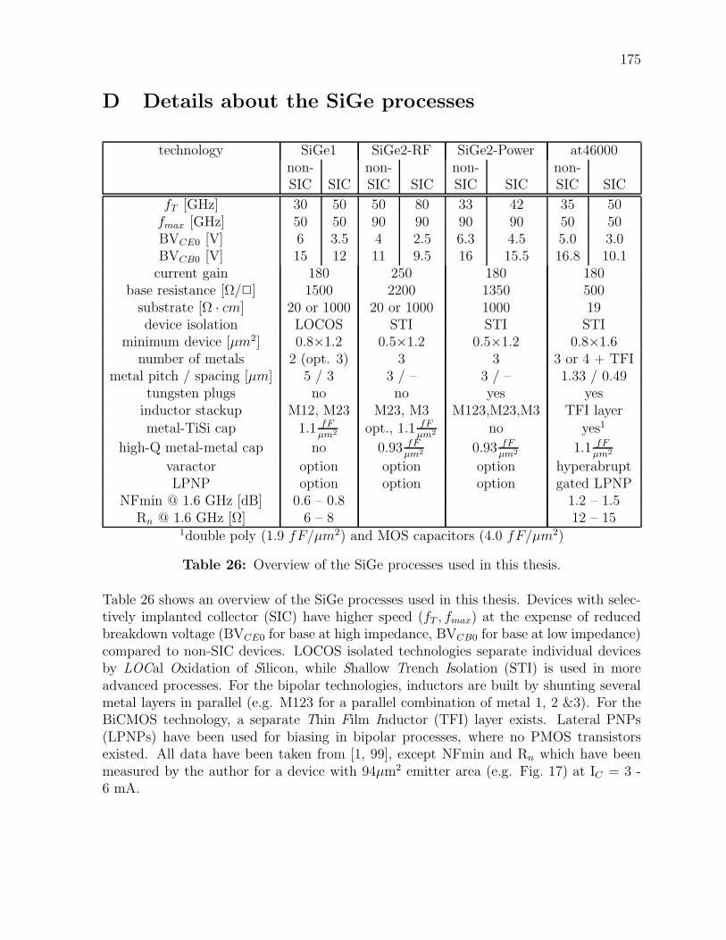
175
D Details about the SiGe processes
technology SiGe1 SiGe2-RF SiGe2-Power at46000non- non- non- non-SIC SIC SIC SIC SIC SIC SIC SIC
fT [GHz] 30 50 50 80 33 42 35 50fmax [GHz] 50 50 90 90 90 90 50 50BVCE0 [V] 6 3.5 4 2.5 6.3 4.5 5.0 3.0BVCB0 [V] 15 12 11 9.5 16 15.5 16.8 10.1current gain 180 250 180 180
base resistance [Ω/2] 1500 2200 1350 500substrate [Ω · cm] 20 or 1000 20 or 1000 1000 19device isolation LOCOS STI STI STI
minimum device [µm2] 0.8×1.2 0.5×1.2 0.5×1.2 0.8×1.6number of metals 2 (opt. 3) 3 3 3 or 4 + TFI
metal pitch / spacing [µm] 5 / 3 3 / – 3 / – 1.33 / 0.49tungsten plugs no no yes yes
inductor stackup M12, M23 M23, M3 M123,M23,M3 TFI layer
metal-TiSi cap 1.1 fFµm2 opt., 1.1 fF
µm2 no yes1
high-Q metal-metal cap no 0.93 fFµm2 0.93 fF
µm2 1.1 fFµm2
varactor option option option hyperabruptLPNP option option option gated LPNP
NFmin @ 1.6 GHz [dB] 0.6 – 0.8 1.2 – 1.5Rn @ 1.6 GHz [Ω] 6 – 8 12 – 15
1double poly (1.9 fF/µm2) and MOS capacitors (4.0 fF/µm2)
Table 26: Overview of the SiGe processes used in this thesis.
Table 26 shows an overview of the SiGe processes used in this thesis. Devices with selec-tively implanted collector (SIC) have higher speed (fT , fmax) at the expense of reducedbreakdown voltage (BVCE0 for base at high impedance, BVCB0 for base at low impedance)compared to non-SIC devices. LOCOS isolated technologies separate individual devicesby LOCal Oxidation of Silicon, while Shallow Trench Isolation (STI) is used in moreadvanced processes. For the bipolar technologies, inductors are built by shunting severalmetal layers in parallel (e.g. M123 for a parallel combination of metal 1, 2 &3). For theBiCMOS technology, a separate Thin Film Inductor (TFI) layer exists. Lateral PNPs(LPNPs) have been used for biasing in bipolar processes, where no PMOS transistorsexisted. All data have been taken from [1, 99], except NFmin and Rn which have beenmeasured by the author for a device with 94µm2 emitter area (e.g. Fig. 17) at IC = 3 -6 mA.
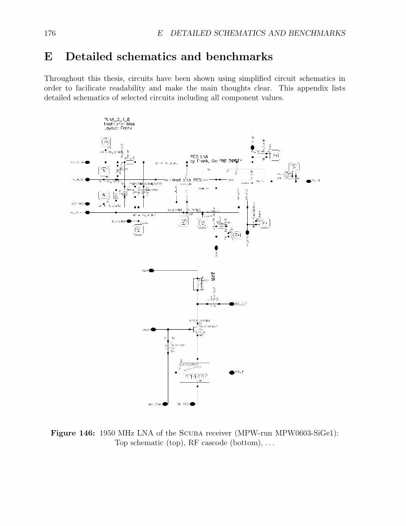
176 E DETAILED SCHEMATICS AND BENCHMARKS
E Detailed schematics and benchmarks
Throughout this thesis, circuits have been shown using simplified circuit schematics inorder to facilicate readability and make the main thoughts clear. This appendix listsdetailed schematics of selected circuits including all component values.
Figure 146: 1950 MHz LNA of the Scuba receiver (MPW-run MPW0603-SiGe1):Top schematic (top), RF cascode (bottom), . . .
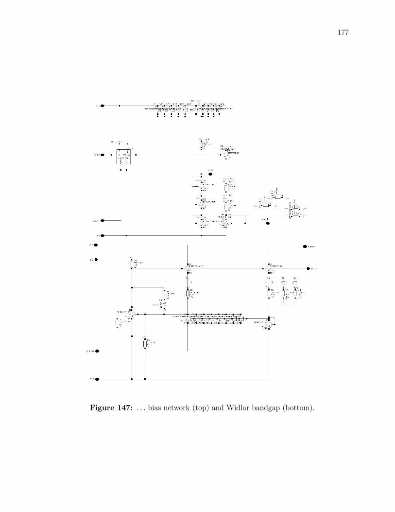
177
Figure 147: . . . bias network (top) and Widlar bandgap (bottom).
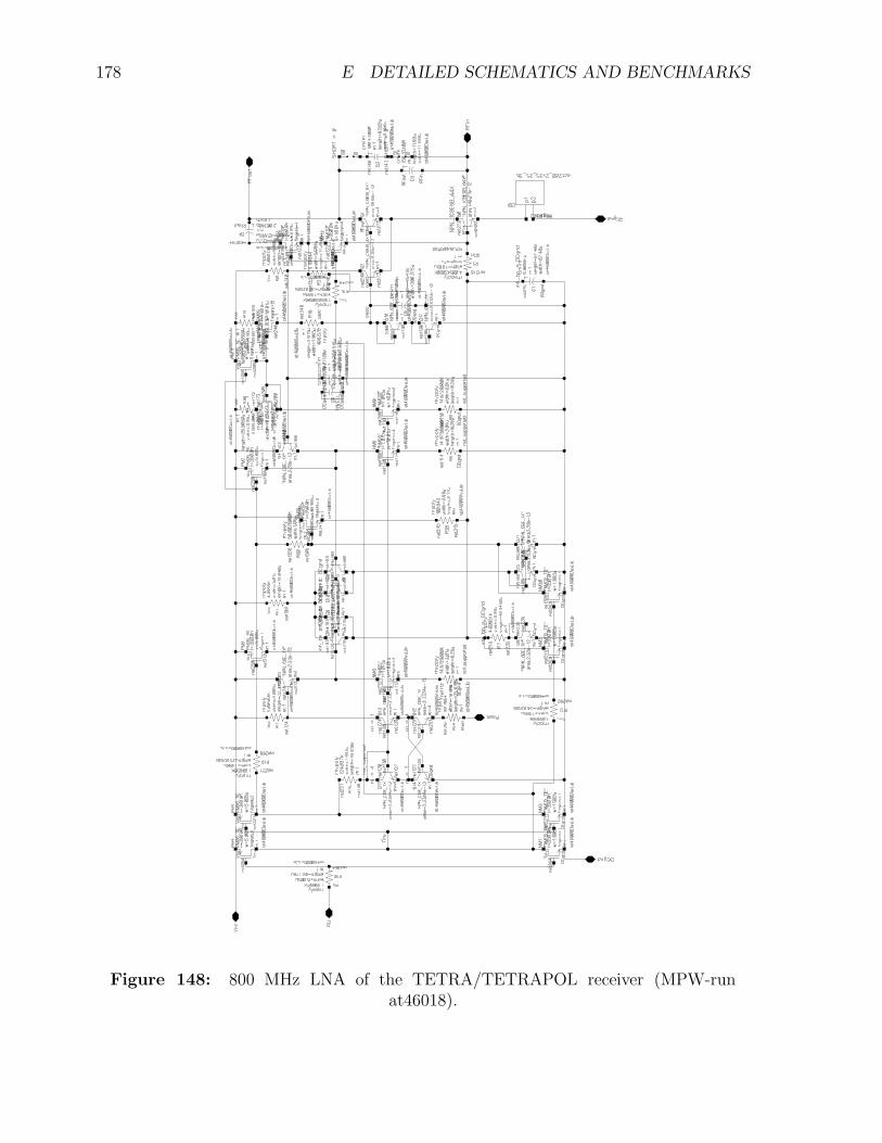
178 E DETAILED SCHEMATICS AND BENCHMARKS
Figure 148: 800 MHz LNA of the TETRA/TETRAPOL receiver (MPW-runat46018).
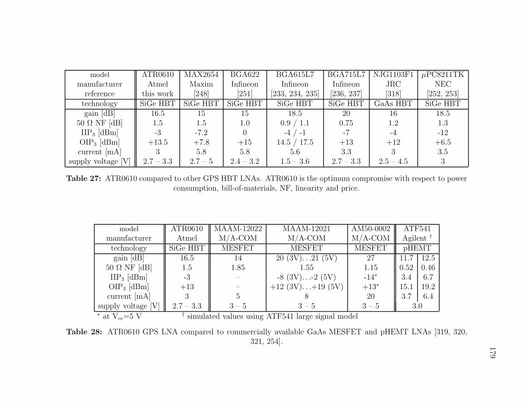
179
model ATR0610 MAX2654 BGA622 BGA615L7 BGA715L7 NJG1103F1 µPC8211TKmanufacturer Atmel Maxim Infineon Infineon Infineon JRC NEC
reference this work [248] [251] [233, 234, 235] [236, 237] [318] [252, 253]technology SiGe HBT SiGe HBT SiGe HBT SiGe HBT SiGe HBT GaAs HBT SiGe HBTgain [dB] 16.5 15 15 18.5 20 16 18.5
50 Ω NF [dB] 1.5 1.5 1.0 0.9 / 1.1 0.75 1.2 1.3IIP3 [dBm] -3 -7.2 0 -4 / -1 -7 -4 -12OIP3 [dBm] +13.5 +7.8 +15 14.5 / 17.5 +13 +12 +6.5current [mA] 3 5.8 5.8 5.6 3.3 3 3.5
supply voltage [V] 2.7 – 3.3 2.7 – 5 2.4 – 3.2 1.5 – 3.6 2.7 – 3.3 2.5 – 4.5 3
Table 27: ATR0610 compared to other GPS HBT LNAs. ATR0610 is the optimum compromise with respect to powerconsumption, bill-of-materials, NF, linearity and price.
model ATR0610 MAAM-12022 MAAM-12021 AM50-0002 ATF541manufacturer Atmel M/A-COM M/A-COM M/A-COM Agilent †
technology SiGe HBT MESFET MESFET MESFET pHEMTgain [dB] 16.5 14 20 (3V). . .21 (5V) 27 11.7 12.5
50 Ω NF [dB] 1.5 1.85 1.55 1.15 0.52 0.46IIP3 [dBm] -3 – -8 (3V). . .-2 (5V) -14∗ 3.4 6.7OIP3 [dBm] +13 – +12 (3V). . .+19 (5V) +13∗ 15.1 19.2current [mA] 3 5 8 20 3.7 6.4
supply voltage [V] 2.7 – 3.3 3 – 5 3 – 5 3 – 5 3.0∗ at Vcc=5 V † simulated values using ATF541 large signal model
Table 28: ATR0610 GPS LNA compared to commercially available GaAs MESFET and pHEMT LNAs [319, 320,321, 254].
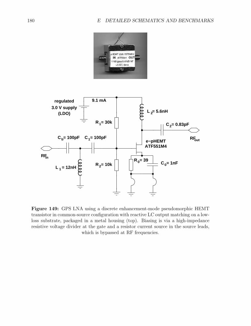
180 E DETAILED SCHEMATICS AND BENCHMARKS
R = 390R = 10k2
R = 30k1
L = 5.6nH2
C = 0.83pF2
C = 100pF1C = 100pFb
L = 12nH1
C = 1nF0
e−pHEMTATF551M4
regulated
3.0 V supply(LDO)
9.1 mA
outRF
inRF
Figure 149: GPS LNA using a discrete enhancement-mode pseudomorphic HEMTtransistor in common-source configuration with reactive LC output matching on a low-loss substrate, packaged in a metal housing (top). Biasing is via a high-impedanceresistive voltage divider at the gate and a resistor current source in the source leads,
which is bypassed at RF frequencies.
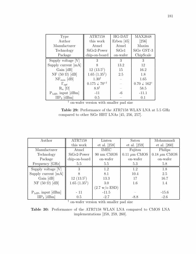
181
Type ATR7158 HG-DAT MAX2648Author this work Erben [45] [256]
Manufacturer Atmel Atmel MaximTechnology SiGe2-Power SiGe1 SiGe GST-3
Package chip-on-board on-wafer ChipScale
Supply voltage [V] 3 3 3Supply current [mA] 8 13.2 12
Gain [dB] 12 (13.5†) 15 16.2NF (50 Ω) [dB] 1.65 (1.35†) 2.5 1.8
NFmin [dB] 1.30† – 1.65Γopt 0.175 6 70 † – 0.70 6 162
Rn [Ω] 8.8† – 58.5P1dB, input [dBm] -11 -6 -11.1
IIP3 [dBm] 0.5 – 0.1† on-wafer version with smaller pad size
Table 29: Performance of the ATR7158 WLAN LNA at 5.5 GHzcompared to other SiGe HBT LNAs [45, 256, 257].
Author ATR7158 Linten Satou Mohammadithis work et al. [258] et al. [259] et al. [260]
Manufacturer Atmel IMEC Fujitsu PhilipsTechnology SiGe2-Power 90 nm CMOS 0.11 µm CMOS 0.18 µm CMOS
Package chip-on-board on-wafer on-wafer on-waferFrequency [GHz] 5.5 5.5 5.3 5.8
Supply voltage [V] 3 1.2 1.2 1.8Supply current [mA] 8 8.1 10.4 2.5
Gain [dB] 12 (13.5†) 13.3 17 16.7NF (50 Ω) [dB] 1.65 (1.35†) 3.0 1.6 1.4
(2.7 w/o ESD)P1dB , input [dBm] - 11 -11.5 – -15.6
IIP3 [dBm] 0.5 -2.7 -8.8 -2.6† on-wafer version with smaller pad size
Table 30: Performance of the ATR7158 WLAN LNA compared to CMOS LNAimplementations [258, 259, 260].
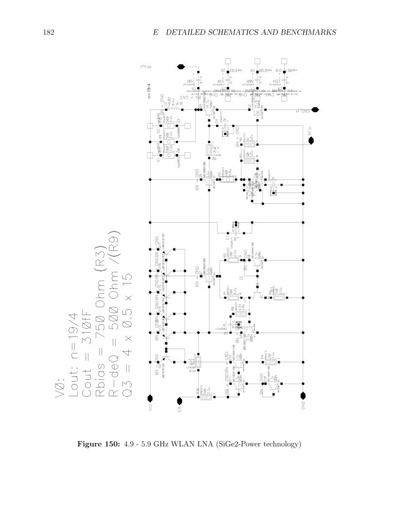
182 E DETAILED SCHEMATICS AND BENCHMARKS
Figure 150: 4.9 - 5.9 GHz WLAN LNA (SiGe2-Power technology)
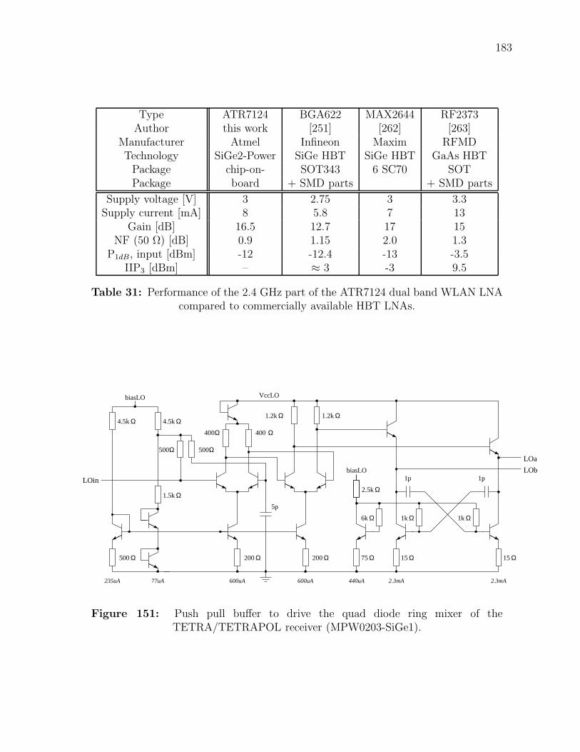
183
Type ATR7124 BGA622 MAX2644 RF2373Author this work [251] [262] [263]
Manufacturer Atmel Infineon Maxim RFMDTechnology SiGe2-Power SiGe HBT SiGe HBT GaAs HBT
Package chip-on- SOT343 6 SC70 SOTPackage board + SMD parts + SMD parts
Supply voltage [V] 3 2.75 3 3.3Supply current [mA] 8 5.8 7 13
Gain [dB] 16.5 12.7 17 15NF (50 Ω) [dB] 0.9 1.15 2.0 1.3
P1dB, input [dBm] -12 -12.4 -13 -3.5IIP3 [dBm] – ≈ 3 -3 9.5
Table 31: Performance of the 2.4 GHz part of the ATR7124 dual band WLAN LNAcompared to commercially available HBT LNAs.
15 Ω15 Ω75
1k Ω6k 1k Ω
2.5k Ω
1.2k ΩΩ1.2k
200 Ω200 Ω
400 400
500500
500 Ω
Ω
1p 1p
Ω Ω
ΩΩ
5p
Ω
Ω1.5k
Ω4.5kΩ4.5k
biasLO VccLO
biasLO
235uA 77uA 600uA 440uA 2.3mA 2.3mA600uA
LOin
LOa
LOb
Figure 151: Push pull buffer to drive the quad diode ring mixer of theTETRA/TETRAPOL receiver (MPW0203-SiGe1).
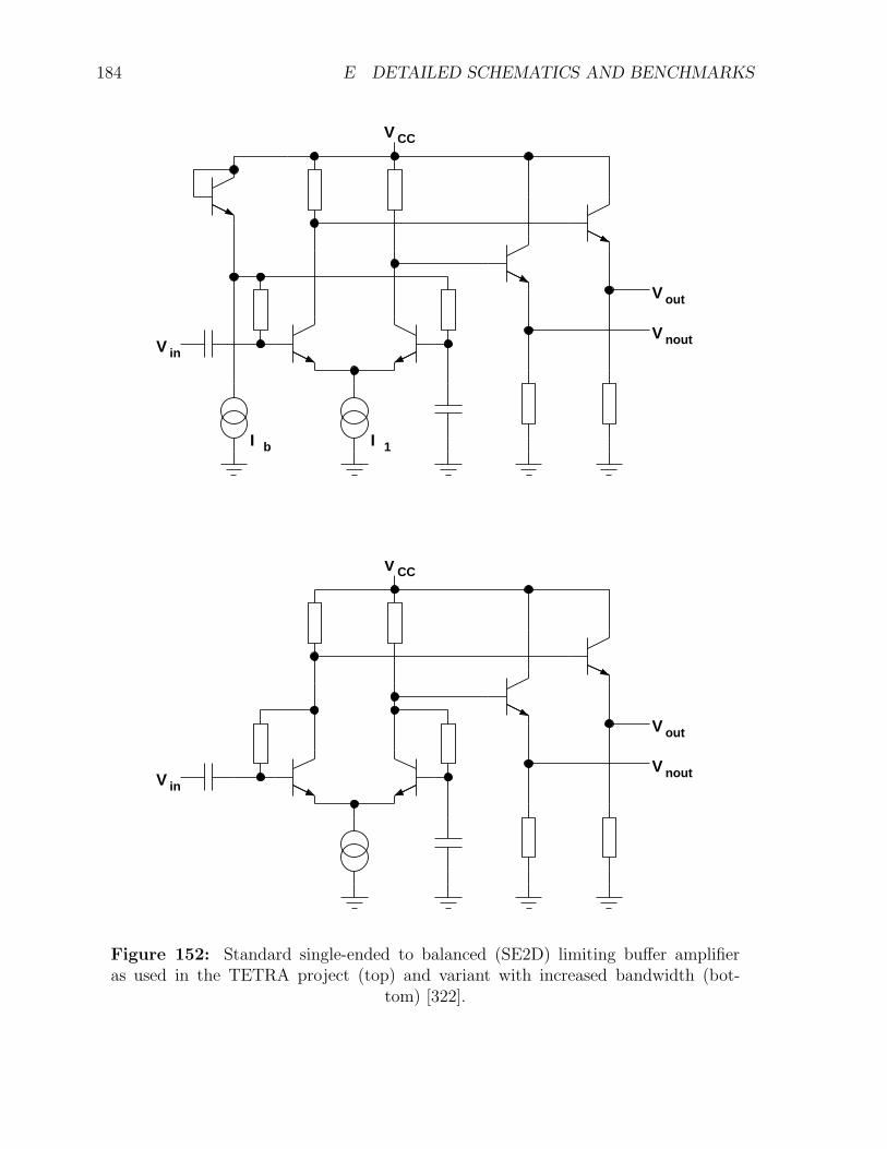
184 E DETAILED SCHEMATICS AND BENCHMARKS
V CC
V nout
V out
V in
I 1I b
V CC
V nout
V out
V in
Figure 152: Standard single-ended to balanced (SE2D) limiting buffer amplifieras used in the TETRA project (top) and variant with increased bandwidth (bot-
tom) [322].
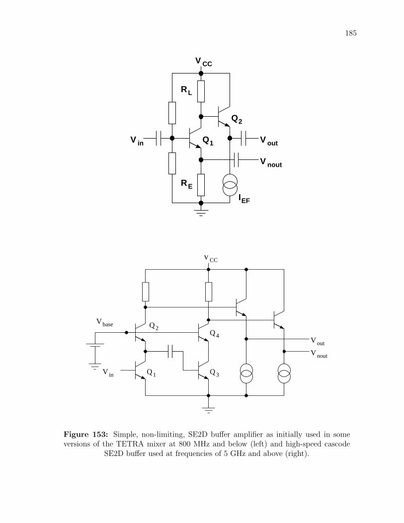
185
V out
V nout
RL
RE
Q1
Q2
V in
V CC
IEF
V in
V base
Q 4
Q 2
Q 1
V out
V nout
Q 3
V CC
Figure 153: Simple, non-limiting, SE2D buffer amplifier as initially used in someversions of the TETRA mixer at 800 MHz and below (left) and high-speed cascode
SE2D buffer used at frequencies of 5 GHz and above (right).
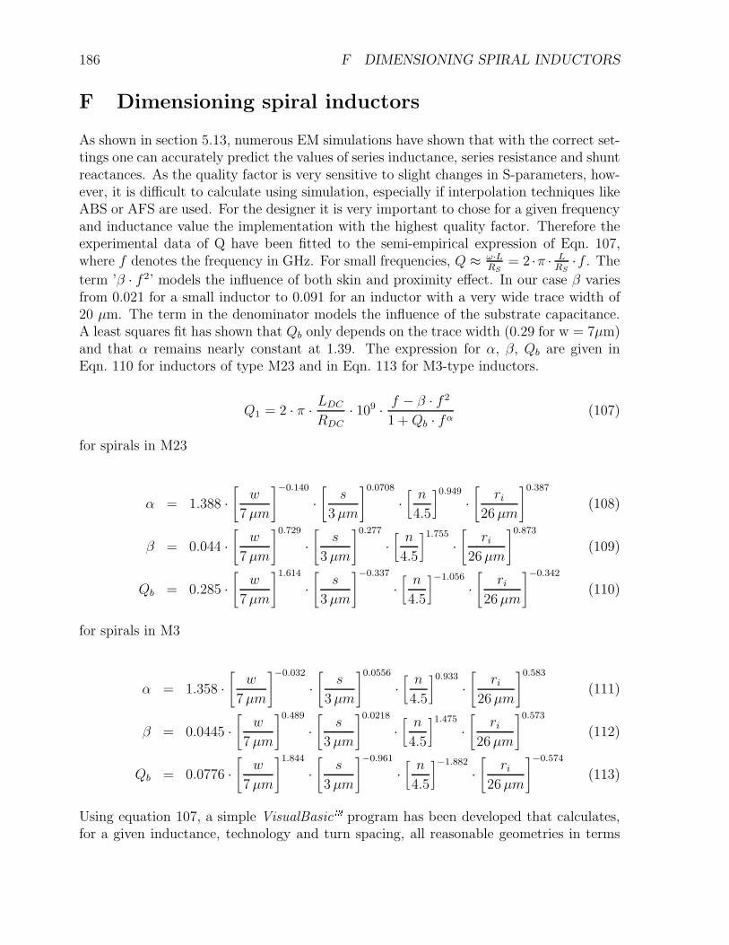
186 F DIMENSIONING SPIRAL INDUCTORS
F Dimensioning spiral inductors
As shown in section 5.13, numerous EM simulations have shown that with the correct set-tings one can accurately predict the values of series inductance, series resistance and shuntreactances. As the quality factor is very sensitive to slight changes in S-parameters, how-ever, it is difficult to calculate using simulation, especially if interpolation techniques likeABS or AFS are used. For the designer it is very important to chose for a given frequencyand inductance value the implementation with the highest quality factor. Therefore theexperimental data of Q have been fitted to the semi-empirical expression of Eqn. 107,where f denotes the frequency in GHz. For small frequencies, Q ≈ ω·L
RS= 2 ·π · L
RS·f . The
term ’β · f 2’ models the influence of both skin and proximity effect. In our case β variesfrom 0.021 for a small inductor to 0.091 for an inductor with a very wide trace width of20 µm. The term in the denominator models the influence of the substrate capacitance.A least squares fit has shown that Qb only depends on the trace width (0.29 for w = 7µm)and that α remains nearly constant at 1.39. The expression for α, β, Qb are given inEqn. 110 for inductors of type M23 and in Eqn. 113 for M3-type inductors.
Q1 = 2 · π · LDC
RDC
· 109 · f − β · f 2
1 + Qb · fα(107)
for spirals in M23
α = 1.388 ·[
w
7 µm
]−0.140
·[
s
3 µm
]0.0708
·[
n
4.5
]0.949
·[
ri
26 µm
]0.387
(108)
β = 0.044 ·[
w
7 µm
]0.729
·[
s
3 µm
]0.277
·[
n
4.5
]1.755
·[
ri
26 µm
]0.873
(109)
Qb = 0.285 ·[
w
7 µm
]1.614
·[
s
3 µm
]−0.337
·[
n
4.5
]−1.056
·[
ri
26 µm
]−0.342
(110)
for spirals in M3
α = 1.358 ·[
w
7 µm
]−0.032
·[
s
3 µm
]0.0556
·[
n
4.5
]0.933
·[
ri
26 µm
]0.583
(111)
β = 0.0445 ·[
w
7 µm
]0.489
·[
s
3 µm
]0.0218
·[
n
4.5
]1.475
·[
ri
26 µm
]0.573
(112)
Qb = 0.0776 ·[
w
7 µm
]1.844
·[
s
3 µm
]−0.961
·[
n
4.5
]−1.882
·[
ri
26 µm
]−0.574
(113)
Using equation 107, a simple VisualBasic program has been developed that calculates,for a given inductance, technology and turn spacing, all reasonable geometries in terms
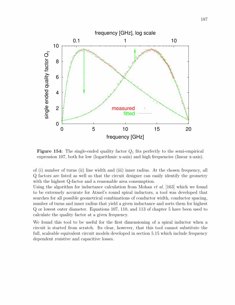
187
0
2
4
6
8
10
0 5 10 15 20
0.1 1 10sin
gle
en
de
d q
ua
lity f
acto
r Q
1
frequency [GHz]
frequency [GHz], log scale
measuredfitted
Figure 154: The single-ended quality factor Q1 fits perfectly to the semi-empiricalexpression 107, both for low (logarithmic x-axis) and high frequencies (linear x-axis).
of (i) number of turns (ii) line width and (iii) inner radius. At the chosen frequency, allQ factors are listed as well so that the circuit designer can easily identify the geometrywith the highest Q-factor and a reasonable area consumption.Using the algorithm for inductance calculation from Mohan et al. [163] which we foundto be extremely accurate for Atmel’s round spiral inductors, a tool was developed thatsearches for all possible geometrical combinations of conductor width, conductor spacing,number of turns and inner radius that yield a given inductance and sorts them for highestQ or lowest outer diameter. Equations 107, 110, and 113 of chapter 5 have been used tocalculate the quality factor at a given frequency.
We found this tool to be useful for the first dimensioning of a spiral inductor when acircuit is started from scratch. Its clear, however, that this tool cannot substitute thefull, scaleable equivalent circuit models developed in section 5.15 which include frequencydependent resistive and capacitive losses.
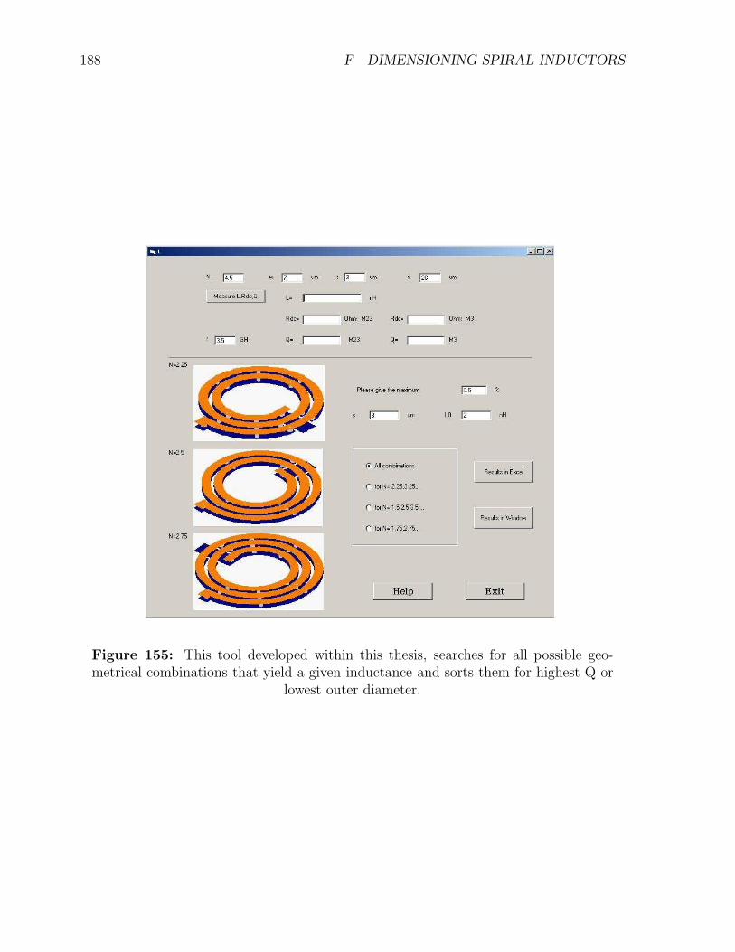
188 F DIMENSIONING SPIRAL INDUCTORS
Figure 155: This tool developed within this thesis, searches for all possible geo-metrical combinations that yield a given inductance and sorts them for highest Q or
lowest outer diameter.
189
G Glossary of terms
Acronym Explanation1G 1st generation mobile technology (analogue)2G 2nd generation mobile technology3G 3rd generation mobile technology
A Emitter area of a transistorAC Alternate CurrentAC coupling Transmission of →RF or →IF signals via a coupling capacitorADS Advanced Design SystemALC Automatic Level ControlAM Amplitude ModulationAMPS Advanced Mobile Phone System (→1G analogue standard in the US)APCO Association of Public Safety Communications Officials InternationalAWGN Average White Gaussian Noise
BAW Electromechanical filters using piezoelectric Bulk-Acoustic-Wave technologyβ Current gain of a bipolar transistorBER Bit Error RateBiCMOS semiconductor process using → bipolar and → CMOS transistorsBJT Bipolar Junction TransistorBL Buried LayerBOM Bill Of MaterialsBPSK Binary Phase Shift KeyingBW Bandwidth
CCK Complementary Code KeyingCDMA Code Division Multiple AccesscdmaOne IS-95 standard-based CDMA system (→2G),
deployed mainly in USA and Asiacdma2000 cdmaOne derivative, accepted as →3G standardCMOS Complementary →MOS transistors (NMOS and PMOS)CMP Chemical-Mechanical-PolishingCOB Chip-on-board mounting of a bare →die onto a →PCBCSP ChipScalePackage: Package having barely larger dimension than
the semiconductor →dieCVD Chemical Vapour Deposition: Technique to deposit a chemical species
from a gaseous mixture (for example silicon from silane = SiH4)
DCR Direct-conversion receiver
190 G GLOSSARY OF TERMS
Die Piece of semiconductor containing the IC after separating the waferDUT Device Under TestDQPSK Differential →QPSKDSSS Direct Sequence Spread SpectrumDiplexer Device that allows bi-directional (duplex) communication over a
single channel
Early Voltage, that models the influence of collector voltage on collector currentin a → BJT
EF Emitter followerEGNOS European Geostationary Navigation Overlay System (overlay to → GPS)ESD ElectroStatic DischargeETSI European Telecommunications Standards Institute
FBAR Filters using thin-Film-Bulk-Acoustic-Resonance technologyFDD Frequency Division DuplexFDMA Frequency Division Multiple Access systemFER Frame error rateFET Field Effect TransistorsFFT Fast Fourier TransformationFIR Finite Impulse Response filterFM Frequency Modulationfmax Maximum frequency of oscillation, where the power gain drops to ’1’fT Transient frequency of the device, where the current gain drops to ’1’FSK Frequency Shift Keying
Γopt Source impedance for optimum noise performanceGaAs Gallium-ArsenideGDSII Database file format which is the de facto industry standard for
data exchange of IC layout artworkGPS Global Positioning Systemgm Transconductance of a transistorGMSK →MSK with Gaussian filteringGSM Global System for Mobile Communication, worldwide →2G standard
HBT Heterojunction Bipolar TransistorHBM Human Body Model (impact of →ESD of the human body onto an IC)HEMT High Electron Mobility TransistorhFE Current gain of a transistorHPSK Hybrid Phase Shift KeyingHiperLAN High Performance Radio LAN, specified by →ETSIHR high-resistivity
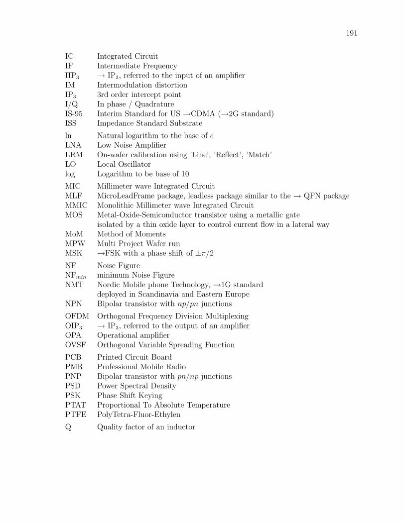
191
IC Integrated CircuitIF Intermediate FrequencyIIP3 → IP3, referred to the input of an amplifierIM Intermodulation distortionIP3 3rd order intercept pointI/Q In phase / QuadratureIS-95 Interim Standard for US →CDMA (→2G standard)ISS Impedance Standard Substrate
ln Natural logarithm to the base of eLNA Low Noise AmplifierLRM On-wafer calibration using ’Line’, ’Reflect’, ’Match’LO Local Oscillatorlog Logarithm to be base of 10
MIC Millimeter wave Integrated CircuitMLF MicroLeadFrame package, leadless package similar to the → QFN packageMMIC Monolithic Millimeter wave Integrated CircuitMOS Metal-Oxide-Semiconductor transistor using a metallic gate
isolated by a thin oxide layer to control current flow in a lateral wayMoM Method of MomentsMPW Multi Project Wafer runMSK →FSK with a phase shift of ±π/2
NF Noise FigureNFmin minimum Noise FigureNMT Nordic Mobile phone Technology, →1G standard
deployed in Scandinavia and Eastern EuropeNPN Bipolar transistor with np/pn junctions
OFDM Orthogonal Frequency Division MultiplexingOIP3 → IP3, referred to the output of an amplifierOPA Operational amplifierOVSF Orthogonal Variable Spreading Function
PCB Printed Circuit BoardPMR Professional Mobile RadioPNP Bipolar transistor with pn/np junctionsPSD Power Spectral DensityPSK Phase Shift KeyingPTAT Proportional To Absolute TemperaturePTFE PolyTetra-Fluor-Ethylen
Q Quality factor of an inductor

192 G GLOSSARY OF TERMS
QAM Quadrature Amplitude ModulationQFN Quad Flat-pack No-lead package: Leadless package similar to the
→ MLF packageQPSK Quadrature Phase Shift Keying
ρ Specific resistance in units of [Ω · cm] or [Ω · m]. ρ = 1/σRF Radio FrequencyRFIC Radio Frequency Integrated CircuitRIE Reactive Ion Etching
σ Conductivity in units of [S/m]. σ = 1/ρSAW Electromechanical filters using piezoelectric Surface-Acoustic-Wave
technologySGP Simple Gummel Poon model for bipolar transistorsSE2D Single-Ended to Differential converterSiGe Silicon-Germanium alloySMD Surface Mount DeviceSOLT On-wafer calibration procedure using ’Short’, ’Open’, ’Load’, ’Thru’SPICE Simulation Program with Integrated Circuits EmphasisSRF Self Resonance FrequencySTI Shallow Trench Isolation, technique to isolate active devices on the wafer
from each other
T Absolute temperature in KelvinTAN → TNATDD Time Division DuplexTDMA Time Division Multiple AccessTETRA TErestrial Trunked RAdio (formerly ’Trans-European Trunked RAdio’)TIA Telecommunications Industry AssociationTIA Transimpedance AmplifierTNA On-wafer calibration using ’Thru’, ’Network’, ’Attentator’TSSOP Thin Shrink Small Outline Package
UMTS Universal Mobile Telephone System (→3G →W-CDMA standard)
U-NII Unlicensed National Information Infrastructure bands (USA)VNA Vector Network AnalyserVSWR Voltage Standing Wave RatioVth Thermal voltage q · T/kB (25.4mV at room temperature)
WCDMA Wideband →CDMA, →3G proposalWLAN Wireless Local Area Networks (license exempt system for data
transmission)

193
H List of symbols
Acronym ExplanationA Ampere or AreaA chain parameterβ current gainC capacitancec0 speed of light in vacuumdB Decibelδ differential operator∆ difference operator or matrix determinantEb energy per data bitεR relative permittivityε0 dielectric contant or vacuum permittivity
ε0 = 1/(µ0 · c2) = 8.854187817... · 10−12A·s/(V·m)f absolute frequencyfT maximum transient frequency (current gain = 0 dB)fmax maximum oscillation frequency (power gain = 0dB)ν frequency offset with respect to a carriergm transconductance gm = δIout
δVin
Γopt generator impedance to achieve minimum noise figure NFmin
h hybrid parameter (h21 = small signal current gain β)I large-signal currenti small-signal current=[ ] imaginary partj
√−1
j0 current densitiy per areaK Kelvink Rollet´s stability factorkB Boltzmann constant (kB = 1.3806504 · 10−23J/K)κ coupling factor between two inductorsµ0 magnetic constant or vacuum permeability
= 4 π 10−7N/A2 = 1.2566370614... · 10−6H/mL inductanceN number of turnsN noise powernH nano HenryNF noise figure
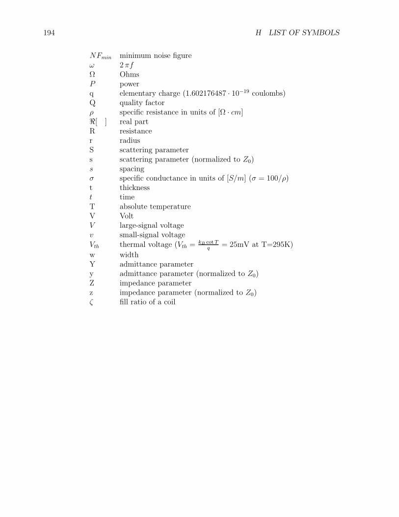
194 H LIST OF SYMBOLS
NFmin minimum noise figureω 2 πfΩ OhmsP powerq elementary charge (1.602176487 · 10−19 coulombs)Q quality factorρ specific resistance in units of [Ω · cm]<[ ] real partR resistancer radiusS scattering parameters scattering parameter (normalized to Z0)s spacingσ specific conductance in units of [S/m] (σ = 100/ρ)t thicknesst timeT absolute temperatureV VoltV large-signal voltagev small-signal voltageVth thermal voltage (Vth = kB cot T
q= 25mV at T=295K)
w widthY admittance parametery admittance parameter (normalized to Z0)Z impedance parameterz impedance parameter (normalized to Z0)ζ fill ratio of a coil
REFERENCES 195
References
[1] www.telefunkensemi.com/#PageTop, last visited Dec. 2009.
[2] “SiGe Bipolar Silicon Germanium – High-speed Technology for CommunicationsApplications,” www.telefunkensemi.com/_assets/Pages/PT-SiGe1.html, lastvisited Dec. 2009.
[3] “Digital Modulation in Communications Systems - An Introduction,” ApplicationNote 1298, Hewlett-Packard Company, 1997.
[4] F. Kostedt and J. C. Kemerling, “Practical GMSK Data Transmission,” ApplicationNote 20830067.002, MX COM, INC., 4800 Bethania Station Road, Winston-Salem,NC, USA, 1998.
[5] “Orthogonal frequency-division multiplexing,” www.en.wikipedia.org/wiki/
OFDM, last visited Dec. 2009.
[6] H. Johnston, “DoCoMo announces trial of 4G system,” wireless europe, p. 12, July2003.
[7] “CDMA - Multiplexing von UMTS,” www.umtslink.at/index.php?
pageid=wcdma, last visited Dec. 2009.
[8] Koninklijke Philips Electronics N.V., “2005 Worldwide Wireless CommunicationStandards,” Dec. 2004. order number 9397 750 14105.
[9] X. Wang, W. Chen, G. Henderson, G. Bergmann, U. Karthaus, and F. Gruson,“SiGe RF Receiver Front-end for Cellular CDMA/GPS Applications,” in IIC-China2003: 8th Annual International IC-China Conference & Exhibition, Mar. 2003.
[10] X. Wang, W. Chen, G. Henderson, G. Bergmann, U. Karthaus, and F. Gruson,“SiGe RF Receiver Front-end for Cellular CDMA/GPS Applications,” in ICC’03:2003 IEEE International Conference on Communications, 2003.
[11] “T0351 – 2.8 V Dual-mode RF receiver for CDMA / AMPS,” data sheet, AtmelGermany GmbH, www.atmel.com, Nov. 2002.
[12] “T0352 – 2.8 V Dual-band/Dual-mode RF receiver for CDMA / AMPS,” data sheet,Atmel Germany GmbH, www.atmel.com, Nov. 2002.
[13] “T0353 – 2.8 V Tri-mode/Quad-mode RF receiver for CDMA / AMPS / GPS,”data sheet, Atmel Germany GmbH, www.atmel.com, Oct. 2002.
[14] “T0354 – 2.8 V Dual-band/Dual-mode RF receiver for Cell CDMA / AMPS,” datasheet, Atmel Germany GmbH, www.atmel.com, Nov. 2002.
196 REFERENCES
[15] U. Karthaus, F. Gruson, T. Bitzer, H. Vogelmann, G. Bergmann, N. Alomari,K. Weese, and A. Pascht, “Fully integrated, 4-channel, direct conversion SiGe re-ceiver IC for UMTS base stations,” in Proc. Eur. Conf. Wireless Technologies 2003,Munich, Germany, pp. 213–216, Oct. 8-10 2003. ISBN: 0-7803-8333-8.
[16] U. Karthaus, F. Gruson, G. Bergmann, and A. Pascht, “Improved four-channeldirect-conversion SiGe receiver IC for UMTS base stations,” IEEE Microwave andWireless Components Letters, vol. 14, pp. 377–379, Aug. 2004. ISSN: 1531-1309.
[17] S. Reynolds, B. Floyd, T. Beukema, T. Zwick, U. Pfeiffer, and H. Ainspan,“A direct-conversion receiver IC for WCDMA,” in Proceedings of the 2002 Bipo-lar/BiCMOS Circuits and Technology Meeting, pp. 61–64, 2002.
[18] J. Jussila, J. Ryynanen, K. Kivakas, L. Sumanen, A. Parssinen, and K. Haionen,“A 22 mA 3.7 dB NF direct conversion receiver for 3G WCDMA,” in Proceedingsof the IEEE International Solid-State Circuits Conference, pp. 284–285, 2001.
[19] T. Bitzer, U. Karthaus, A. Pascht, and K. Weese, “Realisation of a SiGe-HBTDirect Down Conversion Receiver for UMTS Base Stations,” IEEE Int. Symp. onElectron Devices for Microwave and Optoelectronic Applications, Manchester, UK,pp. 83–88, Nov. 2002.
[20] F. Gruson, G. Gaborit, P. Abele, and H. Schumacher, “A broadband SiGe mixerfor 5-GHz WLAN applications with X-band quadrature generation and high image-rejection,” IEEE Radio Frequency Integrated Circuits (RFIC) Symposium, Digest ofPapers, Fort Worth, Texas, USA, pp. 523–526, June 6-8 2004. ISBN: 0-7803-8333-8.
[21] Tetra MOU, “The Madrid tragedy – In the aftermath of disaster, communicationsare the key to efficient response,” Tetra News, no. 2, p. 5, 2004. www.tetramou.
com.
[22] “Sprachlos im Katastrophen-Einsatz - Sicherheitskrafte sollen zuverlassigen Funkbekommen (in german).,” Suddeutsche Zeitung, Feb. 28 2004.
[23] “Terrestrial Trunked Radio,” www.en.wikipedia.org/wiki/Terrestrial_
Trunked_Radio, last visited Dec. 2009.
[24] “Project 25,” www.en.wikipedia.org/wiki/Project_25, last visited Dec. 2009.
[25] P. Lunness, “P25 Radio Systems,” Training Guide TG-001 Rev. 2-0-0, Daniels Elec-tronics Ltd., 43 Erie Street, Victoria, BC Canada V8V 1P8, Jan. 2007.
[26] B. Ellis and C. Komatas, “Will WLAN put 3G in the dark ?,” wireless europe,pp. 17–18, July 2003.
[27] J. P. Maligeorgos and J. R. Long, “A Low-Voltage 5.1-5.8-GHz Image-Reject Re-ceiver with Wide Dynamic Range,” IEEE Journal of Solid-State Circuits, vol. 35,pp. 1917–1926, Dec. 2000.
REFERENCES 197
[28] IEEE Computer Society, “IEEE Standard for Information technology - Telecommu-nications and information exchange between systems - Local and metropolitan areanetworks - Specific requirements Part 11: Wireless LAN Medium Access Control(MAC) and Physical Layer (PHY) Specifications,” June 2007. IEEE Std 802.11-2007.
[29] “HiperLAN,” www.en.wikipedia.org/wiki/HIPERLAN, last visited Dec. 2009.
[30] “HiperLAN2Resource Center,” www.palowireless.com/hiperlan2/about.asp,last visited Dec. 2009.
[31] M. Zargari, D. K. Su, C. P. Yue, S. Rabii, D. Weber, B. Kaczynski, S. S. Mehta,K. Singh, S. Mendis, and B. A. Wooley, “A 5-GHz CMOS transceiver for IEEE802.11a Wireless LAN Systems,” IEEE Journal of Solid-State Circuits, vol. 37,pp. 1688–1693, Dec. 2002.
[32] H. Samavati, H. R. Rategh, and T. H. Lee, “A 5-GHz CMOS Wireless LAN ReceiverFront End,” IEEE Journal of Solid-State Circuits, vol. 35, pp. 765–772, May 2000.
[33] T.-P. Liu and E. Westerwick, “5-GHz CMOS Radio transceiver Front-End Chipset,”IEEE Journal of Solid-State Circuits, vol. 35, pp. 1927–1933, Dec. 2000.
[34] J. Browne, “CMOS Yields High-Speed 5-GHz WLAN Chip Set,” Microwaves & RF,p. 156, Nov. 2000.
[35] “High Frequency Circuit Materials Product Selector Guide,” Tech. Rep. 92-601,Rogers Corporation, 2002.
[36] Maxim Integrated Products, “Single-Chip, 802.11a/b/g Dual-Band RF transceiverDelivers Best Sensitivity,” Analog Design Solutions, 2004.
[37] P. Heide, “Specification for EPCOS WLAN module.” private communications, Jan.2004.
[38] P. Heide, “WLAN-Frontend-Module in LTCC Technologie: Große durch Minia-turisierung,” components - your direct link to EPCOS, vol. 3, pp. 8–10, 2006.EPC:50027.
[39] P. Naraine, “Predicting the EVM Performance of WLAN Power Amplifiers withOFDM Signals,” Microwave Journal, vol. 47, pp. 222–226, May 2004.
[40] Anadigics, “Dual-band WLAN power amp,” Microwave Engineering Europe, p. 36,Dec/Jan 2005.
[41] “Medium Power Amplifier for 5.1 to 5.3 GHz Applications using the MGA-425P8,” Application Note 5085 5989-1507EN, Avago Technologies, Aug. 2004. www.avagotech.com.
198 REFERENCES
[42] “SKY65205: WLAN 802.11b/g RF Front-End Module,” preliminary data sheet,Skyworks Solutions, Inc., Dec. 11 2003.
[43] “SKY65202: WLAN 802.11a RF Front-End Module,” preliminary data sheet, Sky-works Solutions, Inc., Oct. 9 2003.
[44] A. Nakatani and L. Williams, “Automating and Optimizing High PerformanceLTCC Design,” Microwave Journal, vol. 47, pp. 176–188, Sept. 2004.
[45] U. Erben and E. Sonmez, “Fully differential 5 to 6 GHz low noise amplifier usingSiGe HBT technology,” Electronics Letters, vol. 40, pp. 39–41, Jan. 8 2004.
[46] G. Heinrichs, “Galileo – Das neue Europaische Navigationssystem,” in EEEf-COM04: Hochfrequenz- und Mikrowellen-Elektronik, Komponenten und Module, FHUlm, May 26-27 2004.
[47] F. Behbahani, H. Firouzkouhi, R. Chokkalingam, S. Delshadpour, A. Kheirkhahi,M. Nariman, M. Conta, and S. Bhatia, “A Fully Integrated Low-IF CMOS GPS Ra-dio With On-Chip Analog Image Rejection,” IEEE Journal of Solid-State Circuits,vol. 37, pp. 1721–1727, Dec. 2002.
[48] F. Gruson, “COVER FEATURE - GPS : How to design a high-performance GPSreceiver,” Microwave Engineering Europe, pp. 16–19, Aug./Sept. 2006.
[49] H. Schulz, H.-J. Golberg, F. Gruson, M. Durler, and S. J. Spiegel, “GPS low noiseamplifier with high immunity to wireless jamming signals and power control option,”Advances in Radio Science, vol. 2, pp. 195–197, 2004. http://www.adv-radio-sci.net/2/195/2004/,ISSN = 1684-9965.
[50] F. Gruson, H. Schumacher, H. Schulz, H.-J. Golberg, M. Durler, and S. J. Spiegel,“GPS low noise amplifier with high immunity to wireless jamming signals,” in 2004Topical Meeting on Silicon Monolithic Integrated Circuits in RF Systems, Digest ofPapers, (Atlanta), pp. 77–80, Sept. 2004. ISBN: 0-7803-8703-1.
[51] H.-J. Strobel, W. Bischof, S. Gerlach, H. Schulz, K.-F. Becker, E. Jung, K.-D.Lang, H. Mokrani, and S. Spirkovitch, New Combination of SiGe RF Amplifier ICswith High-Q MEMS Components for Wireless Communication Radio transceivers,pp. 97–109. MicroNano Integration, Springer, Berlin, 1 ed., Jan. 2004. ISBN 3-540-20252-8.
[52] E. Alexander, “Leading-edge SAW Filters for Short Range Devices,” MicrowaveJournal, vol. 47, pp. 236–242, May 2004.
[53] “Galileo (Satellitennavigation),” http://en.wikipedia.org/wiki/Galileo_
(satellite_navigation), last visited Dec. 2009.
REFERENCES 199
[54] Clemens Burgi, Eric De Mey, Andrea Orzati, Andreas Thiel, “Highly-IntegratedSolution for Ultra-fast Acquisition and Precise Tracking of Weak GPS and GalileoL1 Signals,” in ION GNSS 19th International Technical Meeting of the SatelliteDivision, pp. 226–235, Sept. 2006.
[55] European Space Agency, “Galileo satellite launch in view,” Microwave EngineeringEurope, pp. 22–23, Oct. 2004.
[56] G. W. Hein, J. Godet, J.-L. Issler, J.-C. Martin, P. Erhard, R. Lucas-Rodriguez,and T. Pratt, “Status of Galileo Frequency and Signal Design,” in Proceedings ofthe 15th International Technical Meeting of the Satellite Division of the Institute ofNavigation ION GPS 2002, pp. 266–277, Sept. 24-27 2002.
[57] “Triple/Dual/Single-Mode CDMA LNA/Mixers,” data sheet, Maxim IntegratedProducts, Sept. 2000. ANJLQ400.03, Rev. B.
[58] V. Aparin, E. Zeisel, and C. Persico, “Highly Linear SiGe BiCMOS LNA and Mixerfor Cellular CDMA/AMPS Applications,” IEEE Radio Frequency Integrated Cir-cuits Symposium, pp. 129–132, 2002.
[59] “Desensitization (telecommunications),” www.en.wikipedia.org/wiki/
Desensitization(telecommunications), last visited Dec. 2009.
[60] I. Kipnis, “Refining CDMA Mobile-Phone Power Control,” Microwaves & RF,pp. 71–76, June 2000.
[61] V. Aparin and C. Persico, “Effect of out-of-band terminations on intermodulationdistortion in common-emitter circuits,” IEEE MTT-S Dig., vol. 3, pp. 977–980,June 1999.
[62] V. Aparin and L. E. Larson, “Modified Derivative Superposition Method for Lin-earizing FET Low Noise Amplifiers,” 2004 IEEE RFIC Symposium, Fort Worth,Texas, USA, no. MO1C-3, 2004.
[63] T. Carey, “Intermodulation Distortion,” Application Note 46891-846, IFR Systems,Inc., 2000.
[64] P. B. Kenington, High-linearity RF amplifier design. Artech House microwave li-brary, Artech House, Norwood, MA, 2000. ISBN 1-58053-143-1.
[65] S. A. Maas, Nonlinear Microwave and RF Circuits. Artech House, Inc., 2nd ed.,2003.
[66] H. Schumacher, Monolithic Microwave ICs in High-Speed Systems. Ulm University,2002. lecture notes.
[67] C. Henn, “Intermodulation distortion (IMD),” Application Bulletin SBOA077,Burr-Brown, 6730 S. Tucson Blvd., Tucson, AZ 85706, U.S.A., Apr. 1994.

200 REFERENCES
[68] “W-CDMA 2.3 GHz VCO using BFR360F and BBY58-02V,” Application Note Rev.2.0, Infineon Technologies AG, 81726 Munchen, Germany, Nov. 2006.
[69] “BAW Duplexer - Serienfertigung gestartet,” components - your direct link to EP-COS, vol. 3, p. 2, 2006. EPC:50027.
[70] R. Aigner, “RF-MEMS Filters Manufactured on Silicon: Key Facts about Bulk-Acoustic-Wave Technology,” in Topical Meeting on Silicon Monolithic IntegratedCircuits in RF Systems, pp. 157–161, Apr. 2003.
[71] J. Browne, “FBAR Filter, Duplexer Isolate PCS Signals,” Microwaves & RF, p. 118,Feb. 2004.
[72] “BAW filters set to sweep the board,” Microwave Engineering Europe, pp. 19–20,Nov. 2004.
[73] “2.7V, Single-Supply, Cellular-Band Linear Power Amplifiers,” data sheet, MaximIntegrated Products, 120 San Gabriel Drive, Sunnyvale, CA, U.S.A., Feb. 2001.19-1524; Rev 3.
[74] “AWT6309 - HELP2AWS/KPCS CDMA 3.4V/28dBm Linear Power AmplifierModule,” data sheet, ANADIGICS, Inc., 141 Mount Bethel Road, Warren, NewJersey 07059, U.S.A., May 2009. Rev 2.4.
[75] H. Friis, “Noise figures of radio receivers,” Proceedings of the IRE, vol. 32, pp. 419–422, 1944.
[76] “Silicon-Germanium HBTs Merge With Mainstream CMOS Process,” ElectronicDesign, p. 97ff, July 10 2000.
[77] M. Bopp, M. Alles, M. Arens, D. Eichel, S. Gerlach, R. Gotzfried, F. Gruson,M. Kocks, G. Krimmer, R. Reimann, B. Ross, M. Siegle, and J. Zieschang, “ADECT Transceiver Chip Set Using SiGe Technology,” in 1999 IEEE InternationalSolid-State Circuits Conference, 1999. Digest of Technical Papers (ISSCC), (SanFrancisco, CA, USA), pp. 68–69, Feb 15-17 1999. ISBN: 0-7803-5126-6.
[78] R. Gotzfried, F. Beisswanger, S. Gerlach, A. Schuppen, H. Dietrich, U. Seiler, K.-H. Bach, and J. Albers, “RFIC’s for Mobile Communication Systems Using SiGeBipolar Technology,” IEEE Transactions on Microwave Theory and Techniques,vol. 46, pp. 661–668, May 1998. ISSN: 0018-9480.
[79] U. Konig and H. Dambkes, “SiGe HBTs AND HFETs,” Solid-State Electronics,vol. 38, no. 9, pp. 1595–1602, 1995.
[80] U. Konig, A. Gruhle, and A. Schuppen, “SiGe Devices and Circuits: Where areAdvantages over III/V ?,” in IEEE GaAs IC Symposium, pp. 14–17, 1995.
REFERENCES 201
[81] A. Schuppen, H. Dietrich, S. Gerlach, H. Hohnemann, J. Arndt, U. Seiler, R.Gotzfried, U. Erben and H. Schumacher, “SiGe technology and components formobile communications systems,” Proc. Bipolar and BiCMOS Topical Meeting,pp. 130–133, Oct. 1996. ISBN: 0-7803-3516-3.
[82] A. Schuppen, H. Dietrich, U.Seiler, H. von der Ropp, and U. Erben, “A SiGe RFtechnology for mobile communication systems,” Microwave Engineering Europe,pp. 39–46, June 1998.
[83] A. Schuppen, J. Berntgen, P. Maier, M. Tortschanoff, W. Kraus and M. Averweg,“An 80GHz SiGe production technology,” BCTM, vol. 14, pp. 42–46, Aug. 2001.
[84] M. Bopp and A. Schuppen, “SiGe Transistor Technology for RF Applications,”Microwave Journal, vol. 42, pp. 22–39, June 1999.
[85] Wolfgang Durr, Uwe Erben, A. Schuppen, H. Dietrich and Hermann Schumacher,“Low-power low-noise active mixers for 5.7 and 11.2GHz using commercially avail-able SiGe HBT MMIC technology,” Electronics Letters, vol. 34, pp. 1994–1996, Oct.1998.
[86] Uwe Erben, Hermann Schumacher, A. Schuppen, H. Dietrich and J. Arndt, “Ap-plication of a Production Ready SiGe HBT Process to 1.9, 5.7 and 10GHz LowNoise MMIC’s,” Topical Meeting on Silicon Monolithic Integrated Circuits in RFSystems, IEEE, Michigan, pp. 100–104, Sept. 1998.
[87] I. Piper, “Build An E-pHEMT Low-Noise Amplifier,” Microwaves & RF, pp. 92–102, Mar. 2004.
[88] “Atmel starts up 82GHz SiGe foundry,” Microwave Engineering Europe, p. 14, Dec.2000 / Jan. 2001.
[89] N. Camilleri, J. Kirchgessner, J. Costa, D. Ngo, and D. Lovelace, “Bondingpad model for silicon VLSI-technologies and their effects on the noise figure ofRF NPNs,” in Microwave and Millimeter-Wave Monolithic Circuit Symposium,pp. 1179–1182, 1994.
[90] J. T. Colvin, S. S. Bhatia, and K. K. O, “Effect of Substrate Resistances on LNAPerformance and a Bondpad Structure for Reducing the Effects in a Silicon BipolarTechnology,” IEEE Journal of Solid-State Circuits, vol. 34, pp. 1339–1344, Sept.1999.
[91] A. Rofougaran, J. Y.-C. Chang, M. Rofougaran, and A. A. Abidi, “A 1 GHz CMOSRF Front-End IC for a Direct-Conversion Wireless Receiver,” IEEE Journal ofSolid-State Circuits, vol. 31, pp. 880–889, July 1996.
202 REFERENCES
[92] H. Schumacher, U. Erben, W. Durr and K.-B. Schad, “Low-Noise, Low-PowerWireless Frontend MMICs Using SiGe HBTs,” IEICE Transactions on Electronics,vol. E82-C, pp. 1943–1950, Nov. 1999. Special Issue on High Frequency / High-Speed Devices for Information and Communication Systems in the 21st Century.
[93] G. Lohninger, “Diskret, aber nicht trivial, Teil 4: Monolithisch integrierteMikrowellen-Bausteine in Si-und SiGe-Technik (in german),” Elektronik, no. 19,pp. 76–83, 2002. www.elektroniknet.de.
[94] “Walter H. Schottky,” last visited Dec. 2009. http://en.wikipedia.org/wiki/
Walter_Schottky.
[95] J.-F. Luy and P. R. (Hrsg.), Silicon-Based Millimeter-Wave Devices, vol. 32 ofSpringer Series in Electronics and Photonics. Heidelberg: Springer-Verlag, 1994.ISBN 3-540-58047-6.
[96] K.M. Strohm, C.N. Rheinfelder, J.-F. Luy, P. Nuchter, T. Hess, W. Heinrich, H.Kuhnert, M. Nadarassin, C. Warns and W. Menzel, “Coplanar and Microstrip Os-cillators in SiGe SIMMWIC Technolopy,” in 2001 IEEE MTT-S International Mi-crowave Symposium Digest, vol. 3, (Phoenix, AZ, USA), pp. 1563–1566, May 20-252001.
[97] A. Muller and E. Kasper, “SIMMWICs on Micromachined Silicon on Insulator Sub-strates beyond 100 GHz,” in IEEE Topical Meeting on Silicon Monolithic IntegratedCircuits in RF Systems SiRF, (Orlando Florida), pp. 22–29, Jan 23-25 2008.
[98] A. Horn and A. Kruck, “Overview of the technical and geometrical parametersfor electromagnetic field simulation,” Tech. Rep. 4.3, Atmel Germany GmbH, Aug.2003.
[99] D. Carver, “AT46000 Design Rule Manual, 0.35µm SiGe BiCMOS Technology,”design rule manual v0.6, Atmel Corporation, Colorado Springs, CO 80906, Nov.2003.
[100] L. Eccles, “Altered Silicon Increases Chip Speeds Up To 35%,” Electronic Design,pp. 29–30, July 23 2001.
[101] “Raising the bar on transistor performance,” Electronic Design Europe, p. 8, Nov.2003.
[102] “Texas Instruments Sees Its 90nm Process Performance Exceed Earlier GenerationBy Over 50%,” Electronics Express, Nov. 2003.
[103] P. MacAdam and B.-G. Goldberg, “CMOS SOS for Mixed-Signal ICs,” AppliedMicrowave & Wireless, pp. 26–37, Feb. 2002.
REFERENCES 203
[104] S. Richard, “A 5.8 GHz WLAN Receiver using RFCMOS Technology,” Master’sthesis, Ulm University, July 2003.
[105] C. C. Enz and Y. Cheng, “MOS Transistor Modelling for RF IC Design,” IEEETransactions on Solid-State Circuits, vol. 35, Feb. 2000.
[106] “MicroLeadFrame(MLF) Package,” data sheet, Amkor Technology, Nov. 2001.www.amkor.com.
[107] “Application Notes for Surface Mount Assembly of Amkor’s MicroLeadFrame(MLF) Packages,” tech. rep., Amkor Technology, Mar. 2001. Rev. B.
[108] “Thermal Considerations of QFN and Other Exposed-Paddle Packages,” Applica-tion Note HFAN-08.1 (Rev. 0, 11/01), Maxim Integrated Products, 2001.
[109] Joachim N. Burghartz, “Silicon RF Technology - The Two Generic Approaches,”in ESSDERC, pp. 143–153, 1997.
[110] E. Sonmez, P. Abele, K.-B. Schad and H. Schumacher, “MMICs in the 20 GHzRange Using A Commercially Available SiGe Foundry Process,” MIOP, Stuttgart,Germany, May 8-10 2001.
[111] E. Sonmez, A. Trasser, K.-B. Schad, P. Abele and H. Schumacher, “High PowerUltra Compact VCO with Active Reactance Concepts at 24 GHz,” in 31st EuropeanMicrowave Conference, 2001, (London, UK), pp. 1–4, Sept. 24-28 2001.
[112] E. Sonmez, A. Trasser, K.-B. Schad, P. Abele and H. Schumacher, “A single-chip 24GHz receiver front-end using a commercially available SiGe HBT foundry process,”in 2002 IEEE Radio Frequency Integrated Circuits (RFIC) Symposium, (Seattle,USA), pp. 159–162, June 2002.
[113] P. Abele, E. Sonmez, K.-B. Schad, and H. Schumacher, “24 GHz SiGe-MMIC Os-cillator Realized with Lumped Elements in a Production Line,” 30th European Mi-crowave Conference, 2000, pp. 1–3, Oct. 2-6 2000.
[114] F. Gruson, P. Abele, K.-B. Schad, E. Sonmez, and H. Schumacher, “24 GHz Differ-ential SiGe-MMIC Oscillator with Integrated Mixer,” in 2003 Topical Meeting onSilicon Monolithic Integrated Circuits in RF Systems, Digest of Papers, pp. 60–63,April 9-11 2003. ISBN: 0-7803-7787-7.
[115] F. Gruson, G. Bergmann, and H. Schumacher, “A frequency doubler with high con-version gain and good fundamental suppression,” 2004 IEEE MTT-S InternationalMicrowave Symposium Digest, pp. 175–178, June 6-11 2004. ISBN: 0-7803-8331-1.
[116] C. Rheinfelder, K. Strohm, L. Metzger, H. Kibbel, J.-F. Luy, and W. Heinrich,“47GHz SiGe-MMIC Oscillator,” 1999 IEEE MTT-S International Microwave Sym-posium Digest, vol. 1, pp. 5–8, June 1999.
204 REFERENCES
[117] C.N. Rheinfelder, F. Beisswanger, J. Gerdes, F.J. Schmuckle, K.M. Strohm, J.-F. Luy, and W. Heinrich, “A Coplanar 38-GHz SiGe MMIC Oscillator,” IEEEMicrowave and Guided Wave Letters, vol. 6, pp. 398–400, Nov. 1996.
[118] C. N. Rheinfelder, F. J. Beisswanger, and W. Heinrich, “Nonlinear Modeling of SiGeHBTs up to 50 GHz,” IEEE Transactions on Microwave Theory and Techniques,vol. 45, pp. 2503–2508, Dec. 1997.
[119] C. N. Rheinfelder, M. Rudolph, F. J. Beisswanger, and W. Heinrich, “NonlinearModeling of SiGe HBTs up to 50 GHz,” IEEE MTT-S Int. Microwave Symp. Dig.,vol. 2, pp. 877–880, 1997.
[120] K. O, “Estimation Methods for Quality Factors of Inductors Fabricated in Sili-con Integrated Circuit Process Technologies,” IEEE Journal of Solid-State Circuits,vol. 33, pp. 1249–1252, Aug. 1998.
[121] J. N. Burghartz, A. E. Ruehli, K. A. Jenkins, M. Soyuer, and D. Nguyen-Ngoc,“Novel Substrat Contact Structure for High-Q Silicon-Integrated Spiral Inductors,”in International Electron Devices Meeting (IEDM), Technical Digest., pp. 55 – 58,Dec. 7-10 1997.
[122] L. E. Larson, “Integrated Circuit Technology Options for RFIC’s - Present Statusand Future Directions,” IEEE Journal of Solid-State Circuits, vol. 33, pp. 387–399,Mar. 1998.
[123] W. B. Kuhn and N. K. Yanduru, “Spiral Inductor Substrate Loss Modelling inSilicon RFICs,” in RAWCON ’98 Proceedings, pp. 305–308, 1998.
[124] A. Rofougaran, J. Rael, M. Rofougaran, and A. A. Abidi, “A 900 MHz CMOS LC-Oscillator with Quadrature Outputs,” 42nd IEEE International Solid-State CircuitsConference (ISSCC), Digest of Technical Papers, pp. 392–393, Aug. 1996. ISBN:0-7803-3136-2.
[125] J. Craninckx and M. S. Steyaert, “A 1.8 GHz Low-Phase-Noise CMOS VCO UsingOptimized Hollow Spiral Inductors,” IEEE Journal of Solid-State Circuits, vol. 32,pp. 736–744, May 1997.
[126] “Spotlight on substrates at device conference,” Microwave Engineering Europe,pp. 14–15, Feb. 2004.
[127] R. Dekker, K. Dessein, J.-H. Fock, A. Gakis, C. Jonville, O. Kuijken, T. Michielsen,P. Mijlemans, H. Pohlmann, W. Schnitt, C. Timmering, and A. Tombeur, “Sub-strate Transfer: Enabling Technology for RF Applications,” in IEEE Interna-tional Electron Devices Meeting (IEDM ’03), Technical Digest, (Washington DC),pp. 15.4.1–15.4.4, Dec 8-10 2003. ISBN: 0-7803-7872-5.
REFERENCES 205
[128] A. Chin, K. T. Chan, C. H. Huang, C. Chen, V. Liang, J. K. Chen, S. C. Chien, S. W.Sun, D. S. Duh, W. J. Lin, C. Zhu, M. F. Li, S. P. McAlister, and D.-L. Kwong, “RFPassive Devices on Si with Excellent Performance Close to Ideal Devices Designedby Electro-Magnetic Simulation,” in IEEE International Electron Devices Meeting(IEDM ’03), Technical Digest, (Washington DC), pp. 15.5.1–15.5.4, Dec 8-10 2003.ISBN: 0-7803-7872-5.
[129] “at59k design manual,” tech. rep., Atmel, 2003.
[130] S. Jenei, G. Vanhorebreek, S. V. Huylenbroeck, S. Decoutre, and B. Nauwelaers,“High performance modules for integrated passives in silicon technologies,” Mi-crowave Engineering Europe, pp. 41–53, June 2001.
[131] D. Shamiryan, T. Abell, F. Iacopi, and K. Maex, “Low-k dielectric materials,”materials today (Elsevier), pp. 34–39, Jan. 2004.
[132] P. Garrou, “GaAs IC makers lead the way in metals and low-k dielectrics,” Com-poundSemiconductor.Net, July 2002.
[133] T. Yoshimori, “X marks the architectural spot,” Electronic Design Europe, p. 14,Nov. 2003.
[134] “Understanding the Fundamental Principles of Vector Network Analysis,” Applica-tion Note 1287-1, Agilent Technologies, 2000.
[135] J. N. Burghartz, K. A. Jenkins, and M. Soyuer, “Multilevel-spiral inductors us-ing VLSI interconnect technology,” IEEE Electron Device Letters, vol. 17, no. 9,pp. 428–430, 1996. ISSN: 0741-3106.
[136] M. Soyuer, K. A. Jenkins, J. N. Burghartz, H. A. Ainspan, F. J. Canora, S. Pon-napalli, J. F. Ewen, and W. E. Pence, “A 2.4-GHz Silicon Bipolar Oscillator withIntegrated Resonator,” IEEE Journal of Solid-State Circuits, vol. 31, pp. 268–270,Feb. 1996.
[137] J. N. Burghartz, “Progress in RF Inductors on Silicon - Understanding SubstrateLosses,” in International Electron Device Meeting (IEDM), Technical Digest, (SanFrancisco, CA), pp. 523–526, Dec. 6-9 1998.
[138] Y. Cao, R. A. Groves, X. Huang, N. D. Zamdmer, J.-O. Plouchart, R. A. Wachnik,T.-J. King, and C. Hu, “Frequency-Independent Equivalent-Circuit Model for On-Chip Spiral Inductors,” IEEE Journal of Solid-State Circuits, vol. 38, pp. 419–426,Mar. 2003.
[139] S. Verma and J. M. Cruz, “On-chip Inductors and Transformers,” Tech. Rep. SMLITR-99-79, Sun Microsystems, Inc., 901 San Antonio Road, Palo Alto, CA 94303,U.S.A, Dec. 1999. http://research.sun.com/techrep/1999/abstract-79.html.
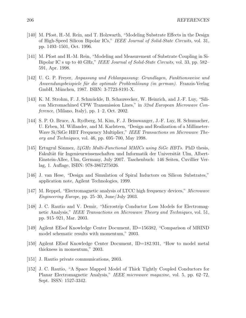
206 REFERENCES
[140] M. Pfost, H.-M. Rein, and T. Holzwarth, “Modeling Substrate Effects in the Designof High-Speed Silicon Bipolar ICs,” IEEE Journal of Solid-State Circuits, vol. 31,pp. 1493–1501, Oct. 1996.
[141] M. Pfost and H.-M. Rein, “Modeling and Measurement of Substrate Coupling in Si-Bipolar IC s up to 40 GHz,” IEEE Journal of Solid-State Circuits, vol. 33, pp. 582–591, Apr. 1998.
[142] U. G. P. Freyer, Anpassung und Fehlanpassung: Grundlagen, Funktionsweise undAnwendungsbeispiele fur die optimale Problemlosung (in german). Franzis-VerlagGmbH, Munchen, 1987. ISBN: 3-7723-8191-X.
[143] K. M. Strohm, F. J. Schmuckle, B. Schauwecker, W. Heinrich, and J.-F. Luy, “Sili-con Micromachined CPW Transmission Lines,” in 32nd European Microwave Con-ference, (Milano, Italy), pp. 1–2, Oct. 2002.
[144] S. P. O. Bruce, A. Rydberg, M. Kim, F. J. Beisswanger, J.-F. Luy, H. Schumacher,U. Erben, M. Willander, and M. Karlsteen, “Design and Realization of a Millimeter-Wave Si/SiGe HBT Frequency Multiplier,” IEEE Transactions on Microwave The-ory and Techniques, vol. 46, pp. 695–700, May 1998.
[145] Ertugrul Sonmez, 24GHz Multi-Functional MMICs using SiGe HBTs. PhD thesis,Fakultat fur Ingenieurwissenschaften und Informatik der Universitat Ulm, Albert-Einstein-Allee, Ulm, Germany, July 2007. Taschenbuch: 146 Seiten, Cuvillier Ver-lag, 1. Auflage, ISBN: 978-3867275026.
[146] J. van Hese, “Design and Simulation of Spiral Inductors on Silicon Substrates,”application note, Agilent Technologies, 1999.
[147] M. Reppel, “Electromagnetic analysis of LTCC high frequency devices,” MicrowaveEngineering Europe, pp. 25–30, June/July 2003.
[148] J. C. Rautio and V. Demir, “Microstrip Conductor Loss Models for Electromag-netic Analysis,” IEEE Transactions on Microwave Theory and Techniques, vol. 51,pp. 915–921, Mar. 2003.
[149] Agilent EEsof Knowledge Center Document, ID=156382, “Comparison of MRINDmodel schematic results with momentum,” 2003.
[150] Agilent EEsof Knowledge Center Document, ID=182.931, “How to model metalthickness in momentum,” 2003.
[151] J. Rautio private communications, 2003.
[152] J. C. Rautio, “A Space Mapped Model of Thick Tightly Coupled Conductors forPlanar Electromagnetic Analysis,” IEEE microwave magazine, vol. 5, pp. 62–72,Sept. ISSN: 1527-3342.
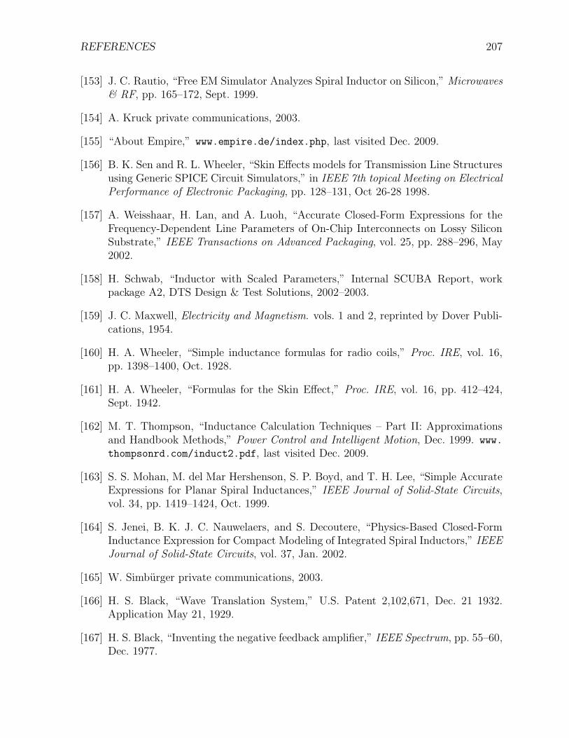
REFERENCES 207
[153] J. C. Rautio, “Free EM Simulator Analyzes Spiral Inductor on Silicon,” Microwaves& RF, pp. 165–172, Sept. 1999.
[154] A. Kruck private communications, 2003.
[155] “About Empire,” www.empire.de/index.php, last visited Dec. 2009.
[156] B. K. Sen and R. L. Wheeler, “Skin Effects models for Transmission Line Structuresusing Generic SPICE Circuit Simulators,” in IEEE 7th topical Meeting on ElectricalPerformance of Electronic Packaging, pp. 128–131, Oct 26-28 1998.
[157] A. Weisshaar, H. Lan, and A. Luoh, “Accurate Closed-Form Expressions for theFrequency-Dependent Line Parameters of On-Chip Interconnects on Lossy SiliconSubstrate,” IEEE Transactions on Advanced Packaging, vol. 25, pp. 288–296, May2002.
[158] H. Schwab, “Inductor with Scaled Parameters,” Internal SCUBA Report, workpackage A2, DTS Design & Test Solutions, 2002–2003.
[159] J. C. Maxwell, Electricity and Magnetism. vols. 1 and 2, reprinted by Dover Publi-cations, 1954.
[160] H. A. Wheeler, “Simple inductance formulas for radio coils,” Proc. IRE, vol. 16,pp. 1398–1400, Oct. 1928.
[161] H. A. Wheeler, “Formulas for the Skin Effect,” Proc. IRE, vol. 16, pp. 412–424,Sept. 1942.
[162] M. T. Thompson, “Inductance Calculation Techniques – Part II: Approximationsand Handbook Methods,” Power Control and Intelligent Motion, Dec. 1999. www.
thompsonrd.com/induct2.pdf, last visited Dec. 2009.
[163] S. S. Mohan, M. del Mar Hershenson, S. P. Boyd, and T. H. Lee, “Simple AccurateExpressions for Planar Spiral Inductances,” IEEE Journal of Solid-State Circuits,vol. 34, pp. 1419–1424, Oct. 1999.
[164] S. Jenei, B. K. J. C. Nauwelaers, and S. Decoutere, “Physics-Based Closed-FormInductance Expression for Compact Modeling of Integrated Spiral Inductors,” IEEEJournal of Solid-State Circuits, vol. 37, Jan. 2002.
[165] W. Simburger private communications, 2003.
[166] H. S. Black, “Wave Translation System,” U.S. Patent 2,102,671, Dec. 21 1932.Application May 21, 1929.
[167] H. S. Black, “Inventing the negative feedback amplifier,” IEEE Spectrum, pp. 55–60,Dec. 1977.
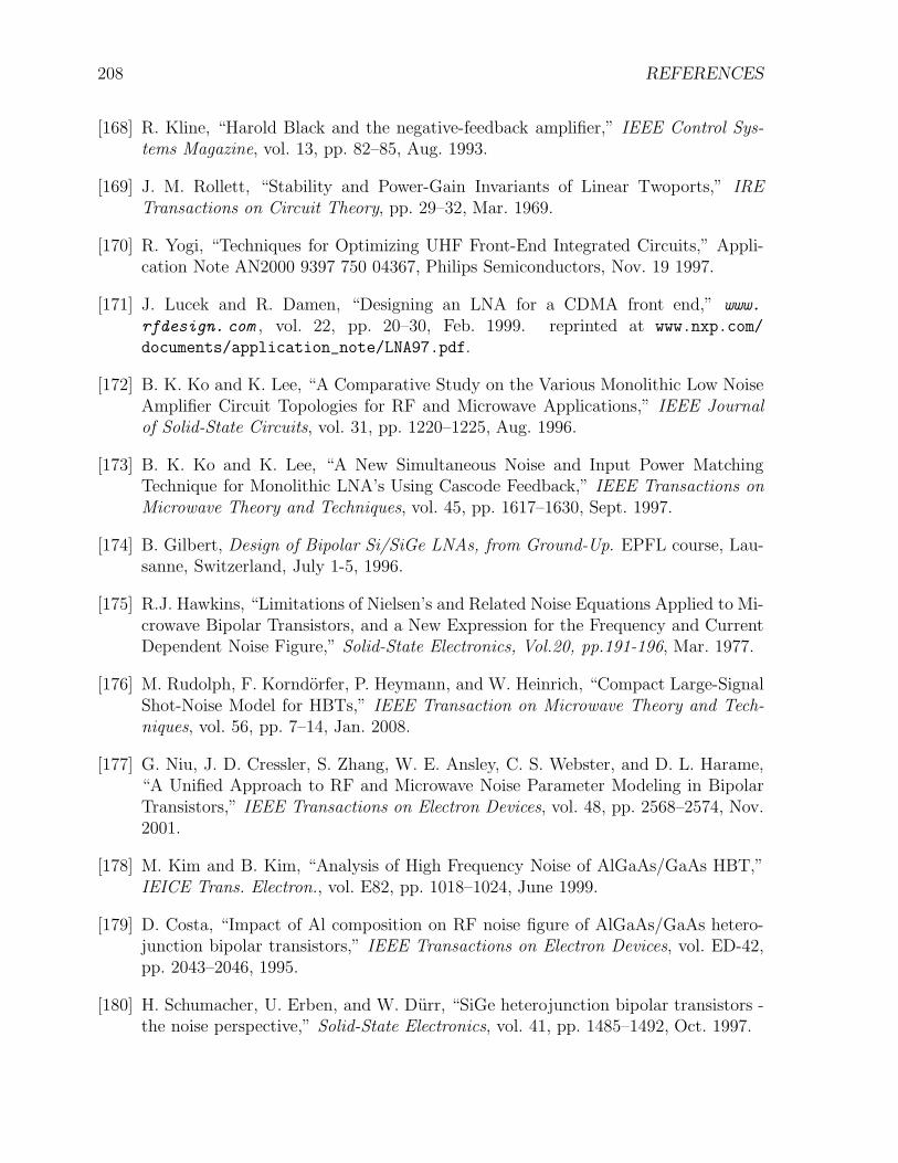
208 REFERENCES
[168] R. Kline, “Harold Black and the negative-feedback amplifier,” IEEE Control Sys-tems Magazine, vol. 13, pp. 82–85, Aug. 1993.
[169] J. M. Rollett, “Stability and Power-Gain Invariants of Linear Twoports,” IRETransactions on Circuit Theory, pp. 29–32, Mar. 1969.
[170] R. Yogi, “Techniques for Optimizing UHF Front-End Integrated Circuits,” Appli-cation Note AN2000 9397 750 04367, Philips Semiconductors, Nov. 19 1997.
[171] J. Lucek and R. Damen, “Designing an LNA for a CDMA front end,” www.
rfdesign. com , vol. 22, pp. 20–30, Feb. 1999. reprinted at www.nxp.com/
documents/application_note/LNA97.pdf.
[172] B. K. Ko and K. Lee, “A Comparative Study on the Various Monolithic Low NoiseAmplifier Circuit Topologies for RF and Microwave Applications,” IEEE Journalof Solid-State Circuits, vol. 31, pp. 1220–1225, Aug. 1996.
[173] B. K. Ko and K. Lee, “A New Simultaneous Noise and Input Power MatchingTechnique for Monolithic LNA’s Using Cascode Feedback,” IEEE Transactions onMicrowave Theory and Techniques, vol. 45, pp. 1617–1630, Sept. 1997.
[174] B. Gilbert, Design of Bipolar Si/SiGe LNAs, from Ground-Up. EPFL course, Lau-sanne, Switzerland, July 1-5, 1996.
[175] R.J. Hawkins, “Limitations of Nielsen’s and Related Noise Equations Applied to Mi-crowave Bipolar Transistors, and a New Expression for the Frequency and CurrentDependent Noise Figure,” Solid-State Electronics, Vol.20, pp.191-196, Mar. 1977.
[176] M. Rudolph, F. Korndorfer, P. Heymann, and W. Heinrich, “Compact Large-SignalShot-Noise Model for HBTs,” IEEE Transaction on Microwave Theory and Tech-niques, vol. 56, pp. 7–14, Jan. 2008.
[177] G. Niu, J. D. Cressler, S. Zhang, W. E. Ansley, C. S. Webster, and D. L. Harame,“A Unified Approach to RF and Microwave Noise Parameter Modeling in BipolarTransistors,” IEEE Transactions on Electron Devices, vol. 48, pp. 2568–2574, Nov.2001.
[178] M. Kim and B. Kim, “Analysis of High Frequency Noise of AlGaAs/GaAs HBT,”IEICE Trans. Electron., vol. E82, pp. 1018–1024, June 1999.
[179] D. Costa, “Impact of Al composition on RF noise figure of AlGaAs/GaAs hetero-junction bipolar transistors,” IEEE Transactions on Electron Devices, vol. ED-42,pp. 2043–2046, 1995.
[180] H. Schumacher, U. Erben, and W. Durr, “SiGe heterojunction bipolar transistors -the noise perspective,” Solid-State Electronics, vol. 41, pp. 1485–1492, Oct. 1997.
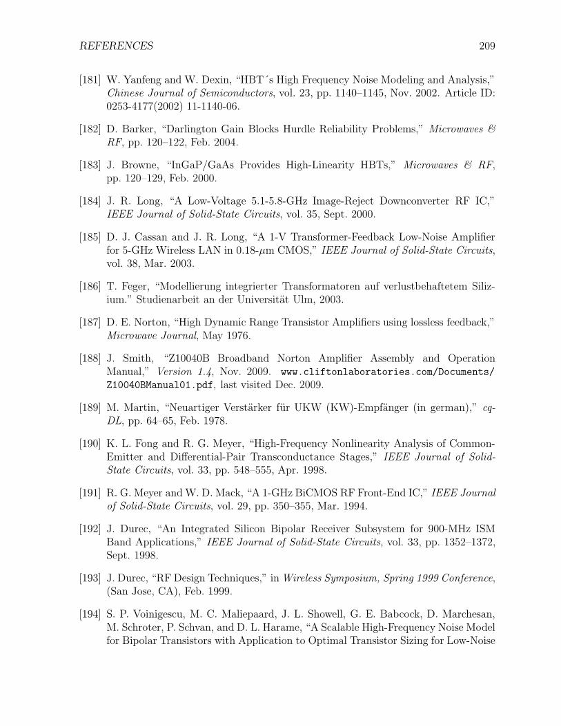
REFERENCES 209
[181] W. Yanfeng and W. Dexin, “HBT´s High Frequency Noise Modeling and Analysis,”Chinese Journal of Semiconductors, vol. 23, pp. 1140–1145, Nov. 2002. Article ID:0253-4177(2002) 11-1140-06.
[182] D. Barker, “Darlington Gain Blocks Hurdle Reliability Problems,” Microwaves &RF, pp. 120–122, Feb. 2004.
[183] J. Browne, “InGaP/GaAs Provides High-Linearity HBTs,” Microwaves & RF,pp. 120–129, Feb. 2000.
[184] J. R. Long, “A Low-Voltage 5.1-5.8-GHz Image-Reject Downconverter RF IC,”IEEE Journal of Solid-State Circuits, vol. 35, Sept. 2000.
[185] D. J. Cassan and J. R. Long, “A 1-V Transformer-Feedback Low-Noise Amplifierfor 5-GHz Wireless LAN in 0.18-µm CMOS,” IEEE Journal of Solid-State Circuits,vol. 38, Mar. 2003.
[186] T. Feger, “Modellierung integrierter Transformatoren auf verlustbehaftetem Siliz-ium.” Studienarbeit an der Universitat Ulm, 2003.
[187] D. E. Norton, “High Dynamic Range Transistor Amplifiers using lossless feedback,”Microwave Journal, May 1976.
[188] J. Smith, “Z10040B Broadband Norton Amplifier Assembly and OperationManual,” Version 1.4, Nov. 2009. www.cliftonlaboratories.com/Documents/
Z10040BManual01.pdf, last visited Dec. 2009.
[189] M. Martin, “Neuartiger Verstarker fur UKW (KW)-Empfanger (in german),” cq-DL, pp. 64–65, Feb. 1978.
[190] K. L. Fong and R. G. Meyer, “High-Frequency Nonlinearity Analysis of Common-Emitter and Differential-Pair Transconductance Stages,” IEEE Journal of Solid-State Circuits, vol. 33, pp. 548–555, Apr. 1998.
[191] R. G. Meyer and W. D. Mack, “A 1-GHz BiCMOS RF Front-End IC,” IEEE Journalof Solid-State Circuits, vol. 29, pp. 350–355, Mar. 1994.
[192] J. Durec, “An Integrated Silicon Bipolar Receiver Subsystem for 900-MHz ISMBand Applications,” IEEE Journal of Solid-State Circuits, vol. 33, pp. 1352–1372,Sept. 1998.
[193] J. Durec, “RF Design Techniques,” in Wireless Symposium, Spring 1999 Conference,(San Jose, CA), Feb. 1999.
[194] S. P. Voinigescu, M. C. Maliepaard, J. L. Showell, G. E. Babcock, D. Marchesan,M. Schroter, P. Schvan, and D. L. Harame, “A Scalable High-Frequency Noise Modelfor Bipolar Transistors with Application to Optimal Transistor Sizing for Low-Noise
210 REFERENCES
Amplifier Design,” IEEE Journal of Solid-State Circuits, vol. 32, pp. 1430–1438,Sept. 1997.
[195] E. Heaney, F. McGrath, P. O’Sullivan, and C. Kermarrec, “Ultra Low Power LowNoise Amplifiers for Wireless Communications,” in 1993 IEEE GaAs IC Symposium,(Santa Clara, CA), pp. 49–51, Oct. 10-13 1993.
[196] T. Chen, “Balance Trade-Offs In GaAs FET LNAs,” Microwaves & RF, pp. 55–57,Feb. 2000.
[197] J.-S. Goo, H.-T. Ahn, D. J. Ladwig, Z. Yu, T. H. Lee, and R. W. Dutton, “ANoise Optimization Technique for Integrated Low-Noise Amplifiers,” IEEE Journalof Solid-State Circuits, vol. 37, pp. 994–1001, Aug. 2002.
[198] B. Battaglia, “Design A Low-Noise Communications Amplifier,” Microwaves & RF,pp. 59–64, Dec. 1999.
[199] M. Williams, “The Cascode Amplifier: A Useful RF Building Block,” MicrowaveProduct Digest, Mar. 1999.
[200] Q. Huang, F. Piazza, P. Orsati, and T. Ohguro, “The Impact of Scaling Down toDeep Submicron on CMOS RF Circuits,” IEEE Journal of Solid-State Circuits,vol. 33, pp. 1023–1036, July 1998.
[201] F. Gruson, “Voltage references and bias networks,” in High Speed Devices andCircuits for Analogue Applications beyond 3 GHz, (www.eurotraining.net), June2001.
[202] B. Gilbert, Analogue IC design: the current mode approach, ch. Bipolar CurrentMirrors, pp. 239–296. IEE Circuits and Systems Series 2, Peter Peregrinus Ltd.,1990. ISBN: 9780863412158.
[203] R. Widlar, “New Developments in IC Voltage Regulators,” in 1970 IEEE Interna-tional Solid-State Conference, (Univ. of. Pennsylvania), pp. 158–159, Feb. 1970.
[204] R. Widlar, “New Developments in IC Voltage Regulators,” IEEE Journal of Solid-State-Circuits, vol. SC-6, pp. 2–4, Feb. 1971.
[205] R. Bohme, “Stromstabilisierung in bipolar integrierten Schaltungen,” Elektronik,no. 5, pp. 129–133, 1988.
[206] H. Banba, H. Shiga, A. Umezawa, T. Miyaba, T. Tanzawa, S. Atsumi, and K. Sakui,“A CMOS Bandgap Reference Circuit with Sub-1-V Operation,” IEEE Journal ofSolid-State Circuits, vol. 34, pp. 670–674, May 1999.
[207] P. Malcovati, F. Maliberti, C. Fiocchi, and M. Pruzzi, “Curvature-CompensatedBiCMOS Bandgap with 1-V Supply Voltage,” IEEE Journal of Solid-State Circuits,vol. 36, pp. 1076–1081, July 2001.
REFERENCES 211
[208] B. Gilbert, Analogue IC design: the current mode approach, ch. Current-mode Cir-cuits From A Translinear Viewpoint, pp. 74–76. IEE Circuits and Systems Series2, Peter Peregrinus Ltd., 1990. ISBN: 9780863412158.
[209] A. Dao, “Integrated LNA and Mixer Basics,” Application Note 884, National Semi-conductor, 1993.
[210] R. Damen private communications, Sept. 2004.
[211] “Agilent MGA-71543 Low Noise Amplifier with Mitigated Bypass Switch,” DataSheet 5988-4553EN, Avago Technologies, Nov. 2001. www.avagotech.com.
[212] “pHEMT Low Noise Amplifier with Bypass Switch MGA-72543,” Data Sheet 5988-4279EN, Avago Technologies, www.avagotech.com, Oct. 2001.
[213] “Agilent MGA-725M4 Low Noise Amplifier with Bypass Switch In Miniature Lead-less Package,” Data Sheet 5988-4278EN, Avago Technologies, www.avagotech.com,Oct. 2001.
[214] G. Lohninger, “A Low Noise Amplifier at 1.9 GHz offers +14 dBm Input InterceptPoint,” Application Note 031, Siemens Discrete and RF Semiconductors, 1996.
[215] S. Narayanan, “Transistor Distortion Analysis Using Volterra Series Representa-tion,” The Bell System Technical Journal, pp. 991–1024, May-June 1967.
[216] S. Inversen, “The Effect of Feedback on Noise Figure,” Proc. IEEE, vol. 63, pp. 540–542, Mar. 1974.
[217] L. Boglione, R. D. Pollard, and V. Postoyalko, “Analytical Behaviour of the NoiseResistance and the Noise Conductance for a Network with Parallel and Series Feed-back,” IEEE Transaction on Microwave Theory and Techniques, vol. 45, pp. 301–304, Mar. 1997.
[218] H. F. Cooke, “Microwave Transistors, Theory and Design,” Proceedings of the IRE,vol. 59, pp. 1163–1181, Aug. 1971.
[219] H. Fukui, “Noise Measure of Microwave Transistors,” Proc. IRE, vol. 54, pp. 1204–1205, Sept. 1966.
[220] G. Wevers, “A High IIP3 Low Noise Amplifier fir 1900 MHz Applications using theSiGe BFP620 Transistor,” Applied Microwave & Wireless, pp. 64–78, July 2000.
[221] S. Maas, “Why I Hate Base Resistance,” IEEE microwave magazine, pp. 54–60,June 2004.
[222] S. A. Maas, B. L. Nelson, and D. L. Tait, “Intermodulation in HeterojunctionBipolar Transistors,” IEEE Transactions on Microwave Theory and Techniques,vol. 40, pp. 442–448, Mar. 1992.
212 REFERENCES
[223] J. Reynolds, “Nonlinear Distortions and Their Cancellation in Transistors,” IEEETransactions on Electron Devices, vol. ED-12, pp. 595–599, Nov. 1965.
[224] S. Narayanan and H. Poon, “An Analysis of Distortion in Bipolar Transistors UsingIntegral Charge Control Model and Volterra Series,” IEEE Transactions on CircuitTheory, vol. CT-20, pp. 341–351, July 1973.
[225] G. Niu, Q. Liang, J. D. Cressler, C. S. Webster, and D. L. Harame, “RF Linear-ity Characteristics of SiGe HBTs,” IEEE Transactions on Microwave Theory andTechniques, vol. 49, pp. 105–108, Sept. 2001.
[226] J.-S. Ko, H.-S. Kim, B.-K. Ko, B. Kim, and B.-H. Park, “Effect of bias scheme onintermodulation distortion and its use for the design of a PCS TX driver,” in IEEERadio Frequency Integrated Circuits (RFIC) Symposium, Digest of Papers, (Boston,MA), pp. 105–108, June 2000.
[227] M. P. van der Heijden, H. C. de Graaff, and L. C. N. de Vreede, “A Novel Frequency-Independent Third-Order Intermodulation Distortion Cancellation Technique forBJT Amplifiers,” IEEE Journal of Solid-State Circuits, vol. 37, pp. 1176–1183,Sept. 2002.
[228] K. L. Fong, “High-Frequency Analysis of Linearity Improvement Technique ofCommon-Emitter Transconductance Stage Using a Low-Frequency-Trap Network,”IEEE Journal of Solid-State Circuits, vol. 35, pp. 1249–1252, Aug. 2000.
[229] K. L. Fong and D. Szmyd, “Linear LNAs Boast Miniscule Noise Figures At 2 GHz,”Microwaves & RF, pp. 162–164, Feb. 2001.
[230] M. L. Frank, “A low noise biasing technique,” European Patent Application EP 1315 287 A2, Agilent Technologies, May 28 2003.
[231] H. Patterson, “Analysis of Ground Bond Wire Arrays for RFICs,” (Denver, CO),pp. 237–240, June 8-11 1997. ISBN: 0-7803-4063-9.
[232] “MMIC LNAs for Wireless Infrastructure Applications,” Microwave Journal,vol. 46, pp. 130–138, Nov. 2003.
[233] “BGA615L7 Silicon Germanium GPS Low Noise Amplifier,” Data Sheet Rev.1.3,Infineon Technologies AG, Feb. 2007.
[234] “BGA615L7 Silicon Germanium GPS LNA MMIC,” product brief, ordering no.b132-h8725-x-0-7600, Infineon Technologies AG, 2006.
[235] “The BGA615L7 Silicon-Germanium Low Noise Amplifier in GPS Applications,”Application Note 091, Rev. 2.0, Infineon Technologies AG, Jan. 2007.
[236] “BGA715L7 Silicon Germanium GPS Low Noise Amplifier,” Data Sheet Rev 2.1,Infineon Technologies AG, Oct. 2009.
REFERENCES 213
[237] “BGA715L7 SiGe Low Noise Amplifier in GPS Applications,” Application Note161, Rev 1.1, Infineon Technologies AG, July 2008.
[238] J. C. Durec and W.E. Main, “Method and circuit for current regulation,” U.S.Patent 5 754 038, May 19 1998.
[239] F. Gruson, S. Hettich, A. Trasser, and H. Schumacher, “Linear Front-End ICs forTETRA / TETRAPOL Handhelds using SiGe Technology,” in 2004 InternationalSymposium on Signals, Systems, and Electronics (ISSSE’04), Aug. 10-13 2004.
[240] B. Gilbert, Design considerations for active BJT mixers, ch. 23, pp. 837–927. Low-power HF microelectronics; A Unified Approach, London: IEE, 1996.
[241] B. Gilbert, “The MICROMIXER: A Highly Linear Variant of the Gilbert MixerUsing a Bisymmetric Class-AB Input Stage,” IEEE Journal of Solid-State Circuits,vol. 32, pp. 1412–1423, Sept. 1997.
[242] “A Low Parts Count Low Noise Amplifier for GPS Applications using BGA428,”Application Note 62, Rev. 2.0, Infineon Technologies AG, Jan. 2007.
[243] P. Shah, P. Gazzerro, V. Aparin, R. Sridhara, and C. Narathong, “A 2GHz Low-Distortion Low-Noise Two-Stage LNA Employing Low-Impedance Bias Termina-tions and Optimum Inter-Stage Match for Linearity,” in Proceedings of the 26th Eu-ropean Solid-State Circuits Conference (ESSCIRC), (Stockholm, Sweden), pp. 308– 311, Sept. 19-21 2000.
[244] K. Alvarino, H. Bui, S. Coryell, S. Egolf, H. Jiang, C. Lazinbat, E. T. Spears,D. Spooner, and D. A. Teeter, “Next Generation CDMA2000 1X Power AmplifierModules,” Applied Microwave & Wireless, pp. 74–84, May 2002.
[245] L. C. de Vreede, H. C. de Graaff, K. Mouthaan, M. de Kok, J. L. Tauritz, and R. G.Baets, “Advanced Modeling of Distortion Effects in Bipolar Transistors Using theMextram Model,” IEEE Journal of Solid-State Circuits, vol. 31, pp. 114–121, Jan.1996.
[246] Johannes J.E.M. Hageraats, “Broadband amplification with high linearity and lowpower consumption,” international patent application wo 00/45505, Jan. 27 2000.
[247] Johannes J.E.M. Hageraats, “Radio Frequency Amplifier with reduced Intermodu-lation Distortion,” U.S. Patent 6 204 728, Mar. 20 2001.
[248] “1575MHz/1900MHz Variable-IP3 Low-Noise Amplifiers,” data sheet, Maxim Inte-grated Products, 2002. 19-1872; Rev 1.
[249] “Silicon Germanium (SiGe) Technology Enhances Radio Front-End Performance,”application note, Maxim Integrated Products, 2000. AN697.
214 REFERENCES
[250] “MAX2654-MAX2656 S-Parameters and Noise Parameters,” tech. rep., Maxim In-tegrated Products. www.maxim-ic.com.
[251] “BGA622 Silicon Germanium Wide Band Low Noise Amplifier with 2 kV ESDProtection,” Data Sheet Rev. 2.2, Infineon Technologies AG, Apr. 2008.
[252] NEC Electronics, “A Low Noise Amplifier IC for 400 MHz to 2 GHz Applications,”Microwave Journal, pp. 144–148, Apr. 2004.
[253] “NEC’s SiGe Low Noise Amplifier for GPS/Mobile Communications µPC8211TK,”data sheet, California Eastern Laboratories, 2005.
[254] “Agilent ATF-541M4 Low Noise Enhancement Mode Pseudomorphic HEMT ina Miniature Leadless Package,” data sheet, Avago Technologies, 2001. www.
avagotech.com.
[255] K. Browne, “E-PHEMT Promises High Linearity From A Single Supply,” Mi-crowaves & RF, p. 137, Apr. 2001.
[256] “5GHz to 6GHz Low-Noise Amplifier in 6-Pin UCSP,” Data Sheet 19-2492; Rev 1,Maxim Integrated Products, 2003.
[257] “Designing with the MAX2648 5GHz LNA for High-Frequency Stability,” Applica-tion Note 1756, Maxim Integrated Products, 2002.
[258] D. Linten, S. Thijs, M. I. Natarajan, P. Wambacq, W. Jeamsaksiri, J. Ramos,A. Mercha, S. Jenei, S. Donnay, and S. Decoutere, “A 5-GHz Fully Integrated ESD-Protected Low-Noise Amplifier in 90-nm RF CMOS,” IEEE Journal of Solid-StateCircuits, vol. 40, pp. 1434–1441, July 2005.
[259] H. Satou, H. Yamazaki, K. Kobayashi, T. Mori, and Y. Watanabe, “5.3 GHz 1.6dBNF CMOS Low Noise Amplifier Using 0.11 µm Technology,” 2004 IEEE RFICSymposium, Fort Worth, Texas, USA, June 6-8 2004.
[260] B. Mohammadi and C. A. T. Salama, “A 5.8 GHz CMOS LNA for WLAN Appli-cations,” 2004 IEEE RFIC Symposium, Fort Worth, Texas, USA, June 6-8 2004.
[261] T. L. Lee, The Design of CMOS Radio-Frequency Integrated Circuits. CambridgeUniversity Press, 2 ed., Dec. 2003. ISBN: 978-0521835398.
[262] “2.4GHz SiGe, High IP3 Low-Noise Amplifier,” Data Sheet 19-1786; Rev 1, MaximIntegrated Products, Mar. 2003.
[263] “RF2373 3V Low Noise Amplifier / 3V Driver Amplifier,” Data Sheet Rev A8DS081217, RF Micro Devices, Inc., 2006.
[264] A. A. Abidi, “Direct-Conversion Radio transceivers for Digital Communications,”IEEE Journal of Solid-State Circuits, vol. 30, pp. 1399–1410, Dec. 1995.
REFERENCES 215
[265] H. Yoshida, T. Toyoda, T. Arai, and H. Tsurumi, “A low DC offset direct conversionreceiver for W-CDMA with low current consumption,” IEICE Electronics Express,vol. 2, pp. 434–439, August 2005.
[266] X. Ruimin and X. Shaoqiu and Y. Bo, “Devise A Millimeter-Wave PHEMT Mixer,”Microwaves & RF, p. 56 ff., Oct. 2000.
[267] M. L. de la Fuente, J. P. Pascual, and E. Artal, “Analyze And Design A CascodeMESFET Mixer,” Microwaves & RF, pp. 129–138, May 1998.
[268] “CMY210: Ultra-Linear Mixer with Integrated LO Buffer,” Data Sheet AM50-0002,TriQuint Semiconductors, July 2003.
[269] S. Sze, Physics of Semiconductor Devices, ch. 1. New York: John Wiley & Sons,Inc., 2nd ed., 1981.
[270] F. Hasouneh, “Design of a Highly Linear Dual Band LNA for a PMR Front-Endusing SiGe HBT Technology,” Master’s thesis, Ulm University, Oct. 2002.
[271] Atmel Germany GmbH und EADS Telecom Deutschland GmbH, “SUPERSTAR-Leistungstechnologie und Universalplattform fur Sicherheitsfunkanwendungen(MEDEA+ A108),” Anlage zum Zwischenbericht SUPERSTAR, 01/2003 bis06/2003, Forderkennzeichen: 01M 3120 A, July 2003.
[272] R. Hartley, “Single-sideband modulator,” U.S. Patent 1 666 206, Apr. 1928.
[273] J. Crols and M. S. J. Steyaert, “A Single-Chip 900 MHz CMOS Receiver Front-Endwith a High Performance Low-IF Topology,” IEEE Journal of Solid-State Circuits,vol. 30, pp. 1483–1492, Dec. 1995.
[274] S. Lee, K. Jung, W. Kim, H. Ryu, and W. Song, “A 1 GHz Image-Rejection Donw-Converter in 0.8µm CMOS Technology,” IEEE Transactions on Consumer Elec-tronics, vol. 44, pp. 235–239, May 1998.
[275] K. Stadius, P. Jarvio, P. Paatsila, and K. Halonen, “Image-Reject Receivers withImage-Selection Functionality,” in Proc. IEEE International Symposium on Circuitsand Systems, vol. IV, pp. 124–127, 2001.
[276] M. J. Gingell, “Singe Sideband Modulation Using Sequence Asymmetric PolyphaseNetworks,” Elect. Commun., vol. 48, pp. 21–25, 1973.
[277] A. Rofougaran, G. Chang, J. Rael, M. Rofougaran, S.Khorram, M. Ku, E. Roth,A. A. Abidi, and H. Samueli, “A 900 MHz CMOS Frequency-Hopped Spread Spec-trum RF Transmitter IC,” in IEEE 1996 Custom Integrated Circuits Conference,(San Diego, CA), pp. 209–212, May 5-8 1996.
216 REFERENCES
[278] J. van der Tang and D. Kasperkovitz, “A 0.9-2.2GHz Monolithic Quadrature MixerOscillator for Direct-Conversion Satellite Receivers,” in Proc. of the IEEE Interna-tional Solid-State Conference, pp. 88–89, 1997.
[279] M. Zannoth, B. Kolb, J. Fenk, and R. Weigel, “A fully integrated VCO at 2 GHz,”IEEE Journal of Solid-State Circuits, vol. 33, pp. 1987–1991, Dec. 1998.
[280] J. Massen, L. Kuhnke, R. Frank, and F. Gruson, “Abschlussbericht des BMBF-Projektes: KOKON, Kfz-Hochstfrequenzelektronik, Teilvorhaben Continental,”tech. rep., Automotive Distance Control Systems GmbH, 2007.
[281] S. Chartier, T. Feger, T. Purtova, B. Schleicher, and H. Schumacher, “79 GHz fullyintegrated fully differential Si/SiGe HBT amplifier for automotive radar applica-tions,” in Proc IEEE International Conference on Electronics, Circuits and Systems(ICECS), (Nice, France), pp. 1011–1014, Dec. 10-13 2006. urn:nbn:de:bsz:289-vts-63386.
[282] S. Chartier, B. Schleicher, F. Korndorfer, S. Glisic, G. Fischer, and H. Schu-macher, “A Fully Integrated Fully Differential Low-Noise Amplifier for Short RangeAutomotive Radar Using a SiGe:C BiCMOS Technology,” in Proc European Mi-crowave Integrated Circuits (EuMIC) Conference, (Munich, Germany), Oct. 8-102007. urn:nbn:de:bsz:289-vts-63355.
[283] B. S. S. Chartier, G. Fischer, F. Korndorfer, J. Borngraber, T. Feger, and H. Schu-macher, “A Compact Low-Power SiGe:C BiCMOS Amplifier for 77-81 GHz Au-tomotive Radar,” in Proc 2008 IEEE Topical Meeting on Silicon Monolithic ICsin RF Systems (SiRF), (Orlando, FL, USA), pp. 195–198, Jan. 23-25 2008.urn:nbn:de:bsz:289-vts-63003.
[284] J. Greene, “Noisemanship – The Art of Measuring Noise Figures Nearly Independentof Device Performance,” IEEE microwave magazine, pp. 136 + 134, June 2004.reprinted from Proceedings of the IRE, vol. 49, p.1223, 1961.
[285] “Three Methods of Noise Figure Measurement,” Application Note APP 2875,Maxim Integrated Products, Nov. 2003.
[286] G. Lohninger and L. Musiol, “Measure 3 Types of Parameter and You’ll Definea Small Signal RF-Transistor: S-Parameter, Noise-Figure and Intermodulation,”Application Note 008, Infineon Technologies AG, July 2000.
[287] N. Kuhn, “Accurate and Automatic noise figure measurements with standard equip-ment,” IEEE MTT-S International Microwave Symposium Digest, vol. 80, pp. 425–427, May 26-30 1980.
[288] “Noise Figure Measurement Accuracy: The Y-Factor Method,” application note,Agilent Technologies, 2001. 57-2.
REFERENCES 217
[289] P. Robbins, “Using Noise for RF Receiver Built-in Test Applications,” MicrowaveJournal, vol. 47, pp. 138–147, Feb. 2004.
[290] “Improving Noise Figure Measurement,” application note, Noisecom. www.
noisecom.com, last visited Dec. 2009.
[291] “HP 8970 Series Noise Figure Measurement Products,” Product Overview 5091-6049E, Hewlett-Packard Company, June 1999.
[292] “Agilent N8972A, N8973A NFA Series Noise Figure Analyzers,” Technical Specifi-cations 5980-0164E, Agilent Technologies, Apr. 2000.
[293] “ESA-E Series Spectrum Analyzers Noise Figure Measurements Personality,” Ap-plication Note 5989-0215EN, Agilent Technologies, Mar. 2004.
[294] “Agilent ATF-551M4 Low Noise Enhancement Mode Pseudomorphic HEMT in aMiniature Leadless Package,” data sheet, Avago Technologies, www.avagotech.com,2001.
[295] J. Smith, “6 dB Hybrid Coupler Experiments,” Mar. 2008. www.
cliftonlaboratories.com/6_db_hybrid_combiner.htm, last visited Dec. 2009.
[296] “Improve Two-tone, Third Order Testing,” Sept. 1999. www.minicircuits.com/
pages/pdfs/mxr1-18.pdf, last visited Dec. 2009.
[297] “ZESC-2-11+ ZESC-2-11 Coaxial Power Splitter/Combiner 2 Way-0 50 Ω 10 to2000 MHz,” Sept. 2007. www.minicircuits.com.
[298] “Improving Network Analyzer Measurements of Frequency-translating Devices,”Application Note 1287-7, Agilent Technologies, 2000.
[299] “High-frequency performance with low, stable contact resistance on aluminumpads,” Data Sheet INFINITY-DS-0803, Cascade Microtech,Inc., 2003.
[300] “On-Wafer Vector Network Analyzer Calibration and Measurements,” ApplicationNote SOLT-LRRM-APP-1201, Cascade Microtech, Inc. www.cmicro.com/file/
on-wafer-vector-network-analyzer-calibration-and-measurements, lastvisited Dec. 2009.
[301] A. M. E. Safwat and L. Hayden, “Sensitivity Analysis ofCalibration Standards for SOLT and LRRM,” applicationnote, Cascade Microtech, Inc., 2001. www.cmicro.com/file/
sensitivity-analysis-of-calibration-standards-for-solt-and-lrrm,last visited Dec. 2009.
[302] “A Guide to Better Vector Network Analyzer Calibrations for Probe-Tip Measure-ments,” Technical Brief TECHBRIEF4-0694, Cascade Microtech, Inc., 1994.
218 REFERENCES
[303] A. Lord, “Advanced RF Calibration Techniques,” tech. rep., Cascade MicrotechEurope. www.cascademicrotech.com.
[304] Suss Microtec Dresden, SussCal User Manual, 2003.
[305] D. F. Williams and R. B. Marks, “LRM Probe-Tip Calibrations with ImperfectResistors and Lossy Lines,” vol. 24, pp. 32–36, Dec. 1993. www.eeel.nist.gov/
dylan_papers/LRMwithImperfect.pdf, last visited Dec. 2009.
[306] S. Basu and L. Hayden, “An SOLR calibrations for accurate measurement of orthog-onal on-wafer DUTs,” IEEE Microwave Theory and Tech. Symp. Dig.,, pp. 1335–1338, June 8-13 1997. www.cascademicrotech.com.
[307] D. K. Walker and D. F. Williams, “Comparison of SOLR and TRL Calibrations,”Publication of the National Institute of Standards and Technology.
[308] “10 Hints for Making Better Network Analyzer Measurements,” Application Note1291-1B, Agilent Technologies, 2001.
[309] A. Fraser, R. Ares, and R. Gleason, “Introduction to bipolar device GHz measure-ment techniques – A guide for accurate on-wafer measurements on small high-speedsilicon bipolar devices,” application note, Cascade Microtec, Inc. www.cmicro.
com/file/introduction-to-bipolar-device-ghz-measurement-techniques,last visited Dec. 2009.
[310] G. Ulbricht, Netzwerkanalyse, Netzwerksynthese und Leitungstheorie (in german).Teubner Verlag, Mar. 1997. ISBN: 3519001101 (out of print).
[311] “De-embedding and Embedding S-Parameter Networks Using a Vector NetworkAnalyzer,” Application Note 1364-1, Agilent Technologies, 2001.
[312] A. Gleißner, “Instruction for Calibration of Rohde & Schwarz Network AnalyzersZVR and ZVC using the TNA Calibration Method,” private communications, Rohde& Schwarz.
[313] O. Ostwald, “Fragen und Antworten zum Netzwerkanalysator ZVR,” ApplicationNote 1EZ38-3D, Rohde & Schwarz, 1998.
[314] “Calibration Types,” http://www.rohde-schwarz.com/webhelp/zvb/System_
Overview/Calibration/Calibration_Types.htm, last visited Dec. 2009.
[315] U. Stumper, “Uncertainties of VNA S-Parameter Measurements Applying the TANSelf-Calibration Method,” IEEE Transactions on Instrumentation and Measure-ment, vol. 56, pp. 597–600, Apr. 2007. ISSN: 0018-9456.
REFERENCES 219
[316] Stumper, U., “A simple evaluation procedure of the TAN calibration and the in-fluence of non-ideal calibration elements on VNA S-parameter measurements,” Ad-vances in Radio Science, vol. 5, pp. 5–12, 2007. http://www.adv-radio-sci.net/5/5/2007/, ISSN = 1684-9965.
[317] E. P. Vandamme, D. M. M.-P. Schreurs, and C. van Dinther, “Improved Three-StepDe-Embedding Method to Accurately Account for the Influence of Pad Parasiticsin Silicon On-Wafer RF Test-Structures,” IEEE Transactions on Electron Devices,vol. 48, pp. 737–742, Apr. 2001.
[318] “NJG1103F1: 1.5/1.9 GHz Low Noise Amplifier GaAs MMIC,” data sheet, NewJapan Radio Co., Ltd.
[319] “GaAs MMIC Low Noise Amplifiers SOIC-8 Platform,” Application Note M540,M/A-COM, Inc.
[320] “Low Noise Amplifier 1.5 - 1.6 GHz,” data sheet, M/A-COM, Inc. MAAM12021.
[321] “Low Noise Amplifier 1.575 GHz,” data sheet, M/A-COM, Inc. AM50-0002.
[322] J. Mullrich, T. Meister, M. Rest, W. Bogner, A. Schoflin, and H.-M. Rein, “40Gbit/s transimpedance amplifier in SiGe bipolar technology for the receiver inoptical-fibre TDM links,” Electronics Letters, vol. 34, no. 5, pp. 452–453, 1998.