Direct Detection of 6 MV X-rays from a Medical Linear Accelerator ...
28
Published in: Physics in Medicine and Biology, 58 (2013) 4471-82 Direct Detection of 6 MV X-rays from a Medical Linear Accelerator using a Semiconducting Polymer Diode Christopher A. Mills 1,2 , Yit-Fong Chan 1 , Akarin Intaniwet 3 , Maxim Shkunov 2 , Andrew Nisbet 1,4 *, Joseph L. Keddie 1 , and Paul J. Sellin 1 * 1 Department of Physics, University of Surrey, Guildford, Surrey GU2 7XH, UK 2 Advanced Technology Institute, University of Surrey, Guildford, Surrey GU2 7XH, UK 3 School of Renewable Energy, Maejo University, Chiang Mai, Thailand, 50290 4 Department of Medical Physics, Royal Surrey County Hospital NHS Foundation Trust, Egerton Road, Guildford, GU2 7XX, UK *Corresponding authors: [email protected], [email protected] Abstract: Recently, a new family of low-cost X-radiation detectors have been developed, based on semiconducting polymer diodes, which are easy to process, mechanically flexible, relatively inexpensive, and able to cover large areas. To test their potential for radiotherapy applications such as beam monitors or dosimeters, as an alternative to the use of solid-state inorganic detectors, we present the direct detection of 6 MV X-rays from a medical linear accelerator using a thick film, semiconducting polymer detector. The diode was subjected to 4 ms pulses of 6 MV X-rays at a rate of 60 Hz, and produces a linear increase in photocurrent with increasing dose rate (from 16.7 to 66.7 mGy.s -1 ). The sensitivity of the diode was found to range from 13 to 20 nC.mGy -1 .cm -3 , for operating voltages from -50 to -150 V, respectively. The diode response was found to be stable after exposure to doses up to 15 Gy. Testing beyond this dose range was not carried out. Theoretical calculations show that the addition of heavy metallic nanoparticles to polymer films, even at low volume fractions, increases the X-ray sensitivity of the polymer film/nanoparticle composite so that it exceeds that for
Transcript of Direct Detection of 6 MV X-rays from a Medical Linear Accelerator ...

Published in: Physics in Medicine and Biology, 58 (2013) 4471-82
Direct Detection of 6 MV X-rays from a Medical Linear
Accelerator using a Semiconducting Polymer Diode
Christopher A. Mills1,2
, Yit-Fong Chan1, Akarin Intaniwet
3, Maxim Shkunov
2, Andrew
Nisbet1,4
*, Joseph L. Keddie1, and Paul J. Sellin
1*
1 Department of Physics, University of Surrey, Guildford, Surrey GU2 7XH, UK
2 Advanced Technology Institute, University of Surrey, Guildford, Surrey GU2 7XH, UK
3 School of Renewable Energy, Maejo University, Chiang Mai, Thailand, 50290
4 Department of Medical Physics, Royal Surrey County Hospital NHS Foundation Trust, Egerton
Road, Guildford, GU2 7XX, UK
*Corresponding authors: [email protected], [email protected]
Abstract:
Recently, a new family of low-cost X-radiation detectors have been developed, based on
semiconducting polymer diodes, which are easy to process, mechanically flexible, relatively
inexpensive, and able to cover large areas. To test their potential for radiotherapy applications such as
beam monitors or dosimeters, as an alternative to the use of solid-state inorganic detectors, we present
the direct detection of 6 MV X-rays from a medical linear accelerator using a thick film,
semiconducting polymer detector. The diode was subjected to 4 ms pulses of 6 MV X-rays at a rate of
60 Hz, and produces a linear increase in photocurrent with increasing dose rate (from 16.7 to 66.7
mGy.s-1
). The sensitivity of the diode was found to range from 13 to 20 nC.mGy-1
.cm-3
, for operating
voltages from -50 to -150 V, respectively. The diode response was found to be stable after exposure to
doses up to 15 Gy. Testing beyond this dose range was not carried out. Theoretical calculations show
that the addition of heavy metallic nanoparticles to polymer films, even at low volume fractions,
increases the X-ray sensitivity of the polymer film/nanoparticle composite so that it exceeds that for

Published in: Physics in Medicine and Biology, 58 (2013) 4471-82
2
silicon over a wide range of X-ray energies. The possibility of detecting X-rays with energies relevant
to medical oncology applications opens up the potential for these polymer detectors to be used in
detection and imaging applications using medical X-ray beams.
PACS: 07.85.Fv X-ray detectors, 29.20.Ej Linear accelerators, 87.53.Bn Dosimetry of x-rays and
gamma rays, 81.05.Fb Organic semiconductors, 61.82.Pv Radiation effects of polymers.
1. Introduction
Over the past 60 years, radiation oncology apparatus has been developed, based on Linear Particle
Accelerator (LINAC) technology, to provide precision targeting of a beam of X-rays. [van Dyk 2005,
Thwaites 2006] To ensure that the dose from a medical LINAC is delivered accurately the emitted X-
rays should be characterised fully, currently achieved by carefully calibrating the radiotherapy beam
according to dosimetry codes of practice and professional recommendations. [e.g. IAEA 2006, IPEM
2007, Thwaites 2003, IPSM 1991] A variety of detectors are available for the measurement of
incident radiation, based on ionisation chambers, film and luminescence dosimeters, and inorganic
semiconductors, and each have their advantages and disadvantages and specific applications.
[Podgorsak 2005]
Semiconductor detectors employed in radiotherapy applications have typically been based on diodes
containing p-type silicon (which is more resistant to radiation damage [Rikner and Grus 1983] and
provides a lower dark current than its n-type analogue) or metal-oxide semiconductor field-effect
transistors (MOSFETS). [Asensio et. al. 2006, Verellen et. al. 2010] These detectors are particularly
useful for dose measurements or beam imaging due to their ability to directly measure spatial dose
distribution, but are less useful for beam calibration due to their propensity to damage from
accumulated dose and drift due to environmental effects. [Podgorsak 2005] Solid-state detectors do,
however, have an inherent sensitivity advantage (up to 104 times) over gas-phase ionisation chambers:
a lower activation energy is required to produce an ionisation pair (approx. 10 times lower), and the
higher material density leads to a higher efficiency (up to 103 times greater), making them ideal

Published in: Physics in Medicine and Biology, 58 (2013) 4471-82
3
candidates for dosimeter miniaturisation. [Fowler 1963] The semiconductor detectors have a wide
range of application in radiotherapy, [Rosenfeld 2006a, Rosenfeld 2006b] for example, semiconductor
diodes are already used in urinary (bladder) and rectal dose measurements using external beam
radiotherapy and brachytherapy. [Essers and Mijnheer 1999, Waldhausel et. al. 2005] Examples of
some novel solid-state dosimeter materials currently under investigation can be found elsewhere.
[Lansley et. al. 2009, Sellin and Vaitkus 2006, Wang et. al. 2005, Mainwood 2000]
We have recently shown that semiconducting polymers can be used for direct detection of low energy,
“soft” X-rays (50 kV Molybdenum [Mo] X-rays) [Boroumand et al 2007] for which the polymers
have a relatively high attenuation coefficient. Here, we describe the use of semiconducting polymer
diodes for the detection of high energy, “hard” X-rays (6 MV X-rays from a tungsten [W] target)
produced from a medical LINAC. In this case, the attenuation coefficient of the polymer for the high
energy X-rays is approx. 30 times less than that for the lower energy X-rays.
2. Methods
2.1 Materials
Poly([9,9-dioctylfluorenyl-2,7-diyl]-co-bithiophene) (F8T2, number-average molecular weight (Mn)
= 45,000 g.mol-1
, weight-average molecular weight (Mw) = 120,000 g.mol-1
) was prepared as
previously reported. [Theim et. al. 2005] Polyimide (Kapton®, 0.025 mm thick), coated on one side
with aluminium (50-100 nm thick) with a nominal sheet resistance of 2.5 Ω□-1
(ohms per square), was
purchased from Goodfellow Ltd., UK. Indium Tin Oxide (ITO) coated glass, with a nominal sheet
resistance of 25 Ω□-1
and an oxide thickness of 80-120 nm, was purchased from Delta Technology
Ltd., USA (CB-60IN). Toluene (99.99%, Sigma-Aldrich Chemical Co., UK) was used as received.

Published in: Physics in Medicine and Biology, 58 (2013) 4471-82
4
2.2 Detector production
F8T2 (5 wt.% solution in toluene) was spin-cast on top of the aluminium (Al) layer of the aluminium-
coated polyimide or the ITO surface of the ITO-coated glass (ca. 1.5 x 1.5 cm2). The spin processing
conditions for the polymer films were: 1) accelerated at 100 rpm/s to 200 rpm and held for 100 s, 2)
accelerated at 100 rpm/s to 500 rpm and held for 60 s, 3) accelerated at 100 rpm/s to 2000 rpm and
held for 30 s, 4) decelerated at 100 rpm/s. This procedure produced a relatively smooth polymer film
with a thickness of approx. 10 μm. After this, the films were typically dry to the touch; a short period
of drying under atmospheric conditions was however required for some films, before annealing under
vacuum at 110°C for 24 h. The thickness of the polymer layers was subsequently measured using a
surface profilometer (Dektak 8, Veeco Instruments). To complete the diode, gold (Au) or Al
electrodes (100 nm thick, 0.5 x 0.5 cm2), depending on the substrate used, were thermally evaporated
onto the F8T2, through a shadow mask, at a pressure of 10-6
mbar. The diodes were connected to the
measurement electronics through filament wires attached by gold paste to the electrodes. Finally, the
diodes were coated with paraffin wax (0CON-194 Logitech Ltd, UK) by dip coating in the molten
wax. Upon completion, the detectors were stored under nitrogen and in the dark to minimize any
adverse oxidation effects.
2.3 Irradiation experiments
The current-voltage (I-V) characteristics of the diodes were examined using a voltage source-
picoammeter (487, Keithley Instruments, UK) by applying a bias voltage to the appropriate electrode.
2.3.1 Visible light illumination
The photocurrent response of a paraffin wax/Au/10 µm F8T2/ITO diode to visible light was measured
by exposing the diode alternatively to indoor laboratory fluorescent lighting and partial sunlight. The
diode was biased by -50V applied to the ITO, and illuminated through the ITO. The external bias

Published in: Physics in Medicine and Biology, 58 (2013) 4471-82
5
ensured the diode was operated in reverse bias conditions to minimise the dark current (reverse bias
leakage current) in the device. Illuminance levels were measured using a lux meter (Macam R203
Radiometer).
2.3.2 X-ray irradiation
X-ray detection measurements were performed using 6 MV X-rays from a multi-mode linear
accelerator (Clinac iX, Varian USA). For each measurement, the detector was mounted in an open
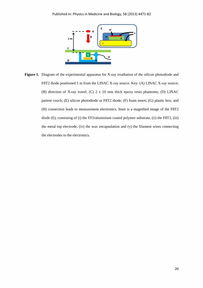
plastic box, to minimise X-ray scatter by metals, and covered by two sheets of 10 mm thick epoxy
resin water-equivalent phantom (RMI451 Gammex Inc., USA) (Figure 1), in order to position the
detector close to the depth of maximum dose. A polyurethane foam insert was used to position the
detector against the rear side of the phantom. During exposure, the detectors were mounted 1 m from
the X-ray source (focus-surface distance [FSD]) with a 10 x 10 cm2 field size. [Radaideh and Alzoubi
2010]
2.3.2.1 Single 6 MV X-ray pulse measurement
The photocurrent response of a silicon photodiode (S1223-01, Hamamatsu Corp.), with an active area
of 0.13 cm2, thickness of 300 μm, and operated at -100V, was measured using an amplifier (DLPCA
200 variable gain, low current, trans-impedance amplifier, FEMTO Messtechnik GmbH) connected to
an oscilloscope (Tektronix 2022B). The diode was exposed to multiple pulses of 6 MV X-rays
providing a dose of 50 mGy/s (= 3 Gy/min). The amplifier was set to provide 104 V/A gain (± 1%),
with a 0.7 µs rise time (10-90%) and 500 kHz bandwidth, and incorporated a 10 Hz low pass filter to
eliminate wideband noise, allowing accurate, low noise DC current measurements down to fA levels.

Published in: Physics in Medicine and Biology, 58 (2013) 4471-82
6
2.3.2.2 Continuous 6 MV X-ray pulse measurement
The photocurrent response of a paraffin wax/Au/10 µm F8T2/Al/Kapton diode was measured, while
applying a constant operating voltage to the Au electrode (-50, -100 or -150V), using the
picoammeter/voltage source. Again, the diode was exposed, through the metal top electrode, to
multiple pulses of 6 MV X-rays with X-ray dose rates of 1 - 4 Gy/min (equivalent to 16.7 - 66.7
mGy/s), but in this case the picoammeter/voltage source was used to measure the average current
output over a 30 s interval. As for the visible light illumination, the diode is operated in reverse bias to
minimise dark current.
2.3.3 Response characterisation
An ideal response to illumination by light, or irradiation by X-rays, would be a “top hat” step
function, such that the response of the diode is instantaneous with the switching on and off of the
incident radiation. [Taylor 2006] Instead, an exponential function characterises the charging and
depletion of the diode (which may be fast but not instantaneous). Using a curve fitting program
(Sigma Plot v8, SPSS Inc) the time constant (τ) - the time to reach 63% of maximum amplitude (or
37% for decaying process) - can be calculated. Figure 2 shows the F8T2 diode response to incident
illumination, whereas Figure 3 shows the photodiode response to incident irradiation. In each case, a
single time constant (τR) could be calculated from the rising signal, but the decay signal was found to
consist of two distinct exponential functions (τD).
Assuming F8T2 is a p-type polymer, it is expected to produce an ohmic contact with the ITO
electrode (due to the similarities in the energies of the Fermi levels of the ITO, approx. -4.7 eV,
[Intaniwet 2010] and that of the semiconductor; the latter of which lies just above the highest
occupied molecular orbital (HOMO) level of the p-type F8T2, approx. -5.0 eV), and a rectifying
contact with the Al contact. [Mills 2009] The response of the diode to incident radiation is due to the
promotion of electrons into the diode conduction band, [Knoll 2000, Pieirls 1955] a process which is
optimised in the depletion region adjacent to the rectifying Al electrode, [Tyagi 1991] and the

Published in: Physics in Medicine and Biology, 58 (2013) 4471-82
7
subsequent removal of the electrons to the external circuit. Conversely, the two exponential decay
components may reflect the movement of electron and hole charge carriers. The drift velocity of the
charges is proportional to the electric field such that,
, (1)
where, µ is the mobility. Rewriting equation 1 to obtain the drift time (td), [Taylor 2006]
, (2)
where, l is the drift length and V is the applied voltage, shows that the drift time is inversely
proportional to the mobility.
3. Results
To allow for comparison with other photodetectors and examine the electrical properties of the F8T2
diode, Figure 2 shows the photocurrent produced by a paraffin wax/Au/10 µm F8T2/ITO diode,
biased at -50 V, exposed alternatively to indoor laboratory fluorescent lighting (approx. 350 lux,
measured using a lux meter) and partial sunlight (approx. 2,000 lux).
A silicon photodiode was used to measure the characteristics of the X-ray pulse from the LINAC.
Figure 3 shows the photocurrent response of the silicon photodiode when exposed to a single 4 µs
pulse of 6 MV X-rays. The inset in figure 3 shows consecutive X-ray pulses detected by the silicon
photodiode detector.
In contrast, the X-ray response of the F8T2 diode is averaged over a number of X-ray pulses (approx.
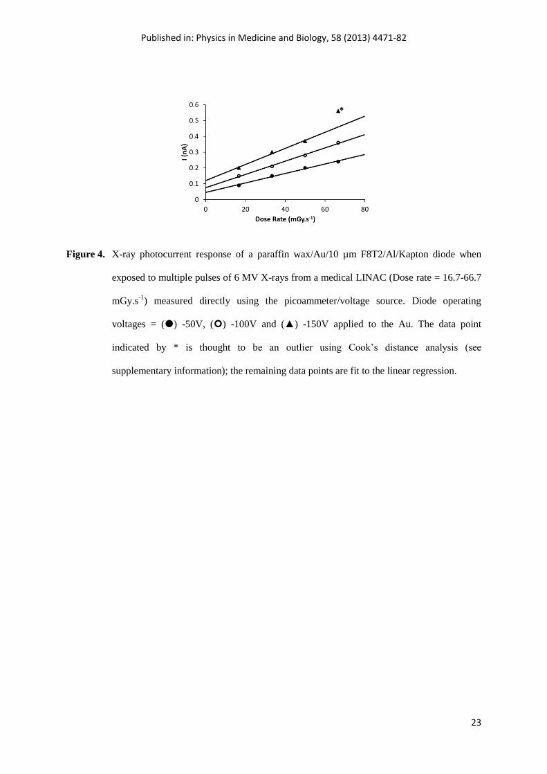
30 s at 60 Hz = 1800 pulses) due to the low current level of the signal produced. Figure 4 shows the
photocurrent response of a paraffin wax/Au/10 µm F8T2/Al/Kapton diode when exposed to multiple
6 MV W X-ray pulses, at dose rates from 16.7 to 66.7 mGy/s, measured directly using the
picoammeter/voltage source.

Published in: Physics in Medicine and Biology, 58 (2013) 4471-82
8
4. Discussion
4.1 F8T2 diode illumination
F8T2 is a chemically stable, conjugated semiconducting polymer, which is soluble in a range of non-
polar solvents because of its pendant alkyl chain moieties on the conjugated polymer backbone. It
displays thermotropic liquid crystallinity, in which the polymer chains can be aligned through thermal
annealing and cooling, allowing for increased chain packing through self-assembly. [Whitehead et. al.
2000] We have previously shown its suitability for the production of flexible, thick film X-radiation
detectors for the detection of soft X-rays. [Mills et. al. 2009] A diode produced from F8T2 has a dark
current of approx. 1.2 nA, but produces 10 nA and 50 nA current, respectively, when exposed to
approx. 350 and 2000 lux visible radiation (Figure 2). Assuming a linear current increase with
increasing illumination (inset Figure 2), this corresponds to a photocurrent sensitivity of 25 pA.lux-1
.
The response of the diode to the light can be quantified. In each case, a single time constant (τR) could
be fitted to the rising signal using the equation, ( ), where τR = ⁄ , but two distinct
exponential functions (τD) were required to fit the decay signal using the equation ( )
( ), where the time constants were τD1 = ⁄ and τD2 = ⁄ . The values of the time constants
and the harmonic mean of the decay constants are given in Table 1. The different time constants
calculated for the illumination at 350 and 2000 lux, from the different light sources (fluorescent lamp
and solar respectively), can be explained to be due to complex charge injection and/or drift due to trap
states in the polymer. [Taylor 2006]
4.2 Irradiation experiments
4.2.1 Silicon photodiode irradiation
Published in: Physics in Medicine and Biology, 58 (2013) 4471-82
9
The silicon photodiode registered pulses from the LINAC that were 16.67 ± 0.25 ms apart (Inset
figure 3), corresponding to a frequency of 60.0 ± 0.9 Hz. [Karzmark and Morton 1998] The
oscilloscope, with a 10 ns measurement interval and 60 µV sensitivity, was then used to isolate a
single, approx. 4 µs pulse response (Figure 3). Measurement of the baseline prior to the pulse gives
the noise level, with an average voltage, VA = 6.6 ± 6.5 mV. The voltage can be converted to current
by dividing by the gain, i.e. VA/104 = 660 ± 650 nA. The response of the silicon photodiode to the 4
µs X-ray pulse gives a peak maximum, Vmax = -552 mV (again, Vmax/104 = -55.2 µA), producing a
signal-to-noise (S/N) ratio of 3,483.
As for the polymer diode, the rise component of the pulse was fit to the equation, ( )
where τR = ⁄ = 1.14 μs (R2 = 0.997). In comparison, the rise time of the amplifier is 0.7 µs. The
rising signal recorded is therefore due to the irradiation of the silicon photodiode and is not apparatus
limited. The decay component was also fit using the equation, ( ) ( ). In this case,
the time constants were τD1 = ⁄ = 0.74 μs, and τD2 = ⁄ = 11.36 μs respectively (R2 = 0.988),
again suggesting that the decay function has fast and slow components.
The X-ray pulse is estimated to be approx. 3.7 μs long, equivalent to 3.77τR. In contrast, the charge in
the photodiode takes approx. 43 μs to decay completely. As the LINAC pulses every 16.67 ms the
photodiode is a capable detector for characterising the LINAC pulse shape. The fast response and
decay for X-ray irradiation mirrors that for the visible light illumination (Table 1), and allows the
characterisation of the individual LINAC pulses at ms time scales.
As previously stated, the drift time is inversely proportional to the mobility (equation 2). For silicon,
the electron and hole mobilities, at 300K, are 1350 and 480 cm2(Vs)
-1 respectively. [Knoll 2000] In
comparison, F8T2 has high hole mobilities (up to 10-2
cm2(Vs)
-1) for a semiconducting polymer, due
to its liquid crystalline character, [Sirringhaus et. al. 2000, Salleo et. al. 2002] and potentially similar
electron mobilities (e.g. 6 x 10⁻³
cm2(Vs)
-1 [Chua et. al. 2005]). The τD values calculated given these
charge mobilities, and using equation 2, are in the region of ns for the silicon and µs for the polymer,

Published in: Physics in Medicine and Biology, 58 (2013) 4471-82
10
and are significantly shorter than the experimental values. This is probably because the response
mechanism, especially in the polymer, will be complex, primarily due to the presence of traps etc.,
[Taylor 2006] and will not necessarily lend itself to simple, optimised electron or hole mobilities.
Even though the diode properties have not been optimised to enhance mobility, the p-type F8T2 has a
proportionally slower response than the silicon diode.
4.2.2 F8T2 diode irradiation
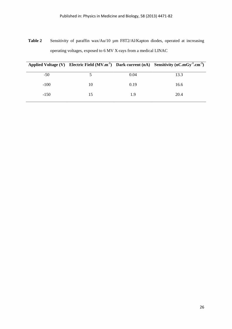
The response of the F8T2 diode (Figure 4) is measured at increasing operating voltages applied to the
Au electrode, giving electric fields through the diode in the range from 5 to 15 MV.m-1
. The diode is
exposed to between 0.5 and 2 Gy per 30 s exposure depending on the dose rate. At the end of the
measurements, it is exposed to 15 Gy in total (5 Gy per set of measurements at each diode operating
voltage [-50, -100 and -150 V]).
The F8T2 diode response is seen to increase linearly with increasing dose rate. The data presented are
corrected for the dark current produced by the device at each voltage, and can be used to calculate the
sensitivity of the diode to 6 MV X-rays (Table 2). The highlighted data point in the -150 V data set is
considered to be an outlier using Cook’s distance analysis (Di > 1, or Di > 4/n) calculated using
Matlab numerical software (the analysis parameters are given in the supplementary data), and hence
the data for the -150 V data set has been fit to a linear regression with the outlier removed (assuming a
linear relationship between the remaining three data points).
The data also display an approximate linear increase in current, for increasing voltage, at constant
dose rates. This is corroborated by examining the data from a similar 10 µm thick F8T2 diode
irradiated with 17.5 keV Tungsten Kα X-rays reported previously, [Mills et. al. 2009] which displayed
a similar approximately linear increase in current with increasing voltage (from -50V to -150V). For
comparison with the values in Table 2, the sensitivity of the reported 10 µm thick F8T2 diode to 17.5
keV X-rays is 158.2 nC/mGy/cm3 when operated at -50 V. [Mills et al. 2009] This sensitivity is

Published in: Physics in Medicine and Biology, 58 (2013) 4471-82
11
approx. 12 times greater at the lower X-ray energy when compared to the irradiation of our F8T2
diode by 6 MV X-rays.
The sensitivity of the diodes at the different incident X-ray energies can be explained by examining
the attenuation coefficient at those energies. The mass attenuation coefficient (µ/ρ) for F8T2 at 17.5
keV is 1.64 cm2g
-1, compared to approx. 0.05 cm
2g
-1 at 2 MeV, given that the average incident X-ray
energy of the 6 MV X-ray beam is approximately 2 MeV; [Hinson et. al. 2008] suggesting that the
F8T2 detector should be approx. 30 times more sensitive to the lower energy X-rays. At 17.5 keV the
majority charge production mechanism is the photoelectric effect, whereas at 2 MeV the predominant
mechanism is Compton scattering. A high energy X-ray in Compton scattering is deflected and, if it
retains enough energy, may go on to produce further Compton or photoelectric effect interactions with
the polymer molecules, which would potentially increase the produced photocurrent. However, due to
the higher energy of the X-ray, the probability of interaction with the atoms of the polymer is reduced,
and the majority of X-rays pass through the polymer without interacting.
4.2.3 Future work: Detector optimisation
Finally, we have recently demonstrated that the integration of heavy metallic/metal oxide
nanoparticles (NPs) into polymer X-ray detectors increases the X-ray induced photocurrent output.
[Intaniwet et. al. 2012, Mills et. al. 2013] Because of their nm-size, NPs can advantageously be added
to the semiconductor polymer without being inter-connected and creating a short-circuit. NPs with a
high atomic number (Z) are strong attenuators of X-radiation, whereas low-Z polymers are not.
Detectors for the characterisation of LINAC X-rays, a high photon flux application where detector
sensitivity does not limit the measurement, are currently based on inflexible solid-state silicon
photodiode detectors (e.g. Scandidos Delta 4 system [Scandidos 2012]). In comparison, an F8T2
diode containing 50 wt.% tantalum (Ta) nanoparticles (equivalent to approx. 10 vol.% Ta) will
attenuate more high energy X-rays (> 1 MeV), up to approx. 80% more attenuation at energies above
Published in: Physics in Medicine and Biology, 58 (2013) 4471-82
12
50 MeV (Figure 5). At lower energies (< 1MeV), the F8T2/Ta diode will attenuate up to eight times
more incident radiation than will the silicon diode, while retaining polymer flexibility.
The polymer films on their own have an energy dependence that is close to that of human tissues
(tissue equivalence) making them attractive for radiotheraphy applications. This tissue equivalence
will worsen for NP loaded polymer films as the concentration of NPs increases, but the inclusion of
the NPs improves the quantum efficiency of the diodes. Even with a low concentration of Ta NPs
(approx. 10 vol.%) the polymer films are potentially seen to be more sensitive to X-rays than Silicon
at a range of energies (Figure 5). For radiotherapy applications a compromise may have to be
determined between tissue equivalence and increased sensitivity.
Because of the mechanical flexibility of the polymer detector, it can be folded. Hence, multiple layers
of the polymer/NP film can be used to attenuate even more of the incident radiation. [Mills et. al.
2013] Improvement of the charge generation and collection from these light-weight, flexible
polymer/NP materials would potentially allow for their integration into disposable adherent plasters to
allow for short duration, real-time detection/imaging of the X-ray beam. Although even thin films of
polymer can be shown to resist high-dose radiation damage over short exposure times, [Kingsley et.
al. 2010] future degradation studies will give an idea of the applicability of such X-ray detectors,
based on polymer semiconductors, to medical applications. [Street et. al. 2012]
5. Conclusions
To be useful as the active component in a radiation dosimeter, semiconducting polymers need to be
compared to the existing technology in a variety of areas. [Podgorsak 2005] The repeatability and
precision of dose measurements using semiconducting polymers have previously been proven for
small numbers of repeat measurements (n = 3) [Mills et. al 2009] with excellent linearity over dose
rates between 10 and 70 mGy.s-1
at X-ray energies of 17.5 keV [Intaniwet et. al. 2010, Intaniwet et. al.
2012]. In this work, linearity was demonstrated for a nominal accelerating potential of 6 MV with a
mean incident energy of 2 MeV (Figure 4). The diodes have also been shown to be stable over long

Published in: Physics in Medicine and Biology, 58 (2013) 4471-82
13
storage periods, with a repeatable response after 6 months, [Intaniwet et. al. 2009] and during
exposure to high doses, e.g. 80 Gy delivered over 20 min. at 67 mGy.s-1
. [Intaniwet et. al. 2012]
Semiconducting polymer diodes also lend themselves to a high spatial resolution and can adapt to
directional dependence. Polymer diodes can be produced with sub-micrometre dimensions,
[Boroumand et. al. 2005] over large areas, [Yu et. al. 2000] and on flexible substrates, [Mills et. al.
2009] and a combination of these technologies will allow them to be positioned three-dimensionally
in an incident radiation beam. As dose is a one-dimensional quantity, [Podgorsak 2005] a dosimeter
with a small volume will have a high spatial resolution. The ability to “fold” a single polymer detector
so that the incident beam passes through it multiple times allows for greater detector sensitivity.
Finally, the rugged, solid-state, semiconducting polymer diodes offer the advantage of a real-time
electrical response, which can be directly read out, and low operating voltages, [Mills et. al. 2009]
which may allow them to be battery operated, increasing their portability.
Here, we have shown that it is possible to directly detect 6 MV X-rays emitted from a medical linear
accelerator using a polymer diode. The currents produced with a non-optimised diode are small (nA)
and require a sensitive ammeter to detect, but with optimisation of the diode architecture to increase
current output the diodes show promise for medical X-ray detection, and potentially for other medical
ionising radiation techniques such as proton beam therapy. [Burnet et. al. 2009, Smith 2006, Levin et.
al. 2005] Detection and imaging of X-ray beams can potentially be achieved by producing flexible
large-area, pixelated diodes, using convenient solution-processing techniques, which could for
example be incorporated into adherent plasters. Finally, the potential to incorporate heavy metallic
nanoparticles in the polymer matrix, at low volume percentages, could also see them rival silicon for
sensitivity to X-rays across the energy spectrum. The challenge for the future is to efficiently collect
the photocurrent produced in the diode by the incident X-rays.
Acknowledgements

Published in: Physics in Medicine and Biology, 58 (2013) 4471-82
14
AI acknowledges funding from the Royal Thai government. The authors acknowledge financial
support through the STFC (grant number: ST/F006667/1), and thank Dr. Heiko Thiem (Evonik
Degussa GmbH, Germany) for the supply of the F8T2 polymer; Dr. Veeramani Perumal, Gary
Strudwick, and Violeta Doukova (all Department of Physics, University of Surrey) for help with
diode preparation and characterisation; and Morgan Ellis (St. Luke’s Cancer Centre, Royal Surrey
County Hospital) for help with completing the LINAC measurements. Also, the authors thank Dr.
Annika Lohstroh (Department of Physics, University of Surrey) for discussions regarding diamond X-
ray dosimetry.
Published in: Physics in Medicine and Biology, 58 (2013) 4471-82
15
References
Asensio L J, Carvajalar M A, López-Villanueva J A, Vilches M, Lallena A M, and Palma A J
2006 Evaluation of a low-cost commercial mosfet as radiation dosimeter Sensors and
Actuators A: Physical 125 288–295
Beaty H W 2000 Handbook of Electrical Power Calculations, 3rd ed., McGraw-Hill Professional,
New York, USA.
Boroumand F A, Fry P W, and Lidzey D G 2005 Nanoscale conjugated-polymer light-emitting
diodes Nano Letters 5 67-71
Boroumand F A, Zhu M, Dalton A B, Keddie J L, Sellin P J, and Gutierrez J J 2007 Direct x-ray
detection with conjugated polymer devices Applied Physics Letters 91 033509
Burnet N G, Kacperek A, Goodman E, and Green S 2009 Proton and particle radiotherapy - a
report on the Franco-British seminar on the future of cancer treatment and imaging using
new physics-based technologies The British Journal of Radiology 82 183-189
Chua L-L, Zaumseil J, Chang J-F, Ou E C-W, Ho P K-H, Sirringhaus H, and Friend R H 2005
General observation of n-type field-effect behaviour in organic semiconductors Nature
434 194-199
Essers M and Mijnheer B J 1999 “In-vivo dosimetry during external photon beam radiotherapy”
International Journal of Radiation Oncology Biology Physics 43 245-259
Fowler J F 1963 Solid state dosimetry Physics in Medicine and Biology 8 1-32
Hinson W H, Kearns W T, deGuzman A F, and Bourland J D 2008 Photon spectral characteristics
of dissimilar 6 MV linear accelerators Medical Physics 35 1698-1702
IAEA 2006 Absorbed dose determination in external beam radiotherapy: An international code of
practice for dosimetry based on standards of absorbed dose to water, International
Atomic Energy Agency TRS 398, Ver 12.
Intaniwet A, Mills C A, Sellin P J, Shkunov M, and Keddie J L 2010 Achieving a Stable Time
Response in Polymeric Radiation Sensors under Charge Injection by X-rays American
Chemical Society (ACS) Applied Materials and Interfaces 2 1692-1699

Published in: Physics in Medicine and Biology, 58 (2013) 4471-82
16
Intaniwet A, Mills C A, Shkunov M, Sellin P J, and Keddie J L 2012 Heavy metallic oxide
nanoparticles for enhanced sensitivity in semiconducting polymer x-ray detectors
Nanotechnology 23 235502
Intaniwet A, Mills C A, Shkunov M, Thiem H, Keddie J L, and Sellin P J 2009 Characterization
of thick film poly(triarylamine) semiconductor diodes for direct x-ray detection Journal
of Applied Physics 106 064513
IPEM 2007 Acceptance Testing and Commissioning of Linear Accelerators, Institute of Physics
and Engineering in Medicine, Report 94, ISBN 978 1 903613 30 6
IPSM 1991 Report of the IPSM working party on low- and medium-energy x-ray dosimetry
Physics in Medicine and Biology 36 1027-1038
Karzmark C J and Morton R J 1998 A Primer on Theory and Operation of Linear Accelerators in
Radiation Therapy, 2nd ed., Medical Physics publishing, Madison, WI.
Kingsley J W, Weston S J, and Lidzey D G 2010 Stability of X-Ray Detectors Based on Organic
Photovoltaic Devices IEEE Journal of Selected Topics in Quantum Electronics 16 1770-
1775
Knoll G F 2000 Radiation Detection and Measurement, 3rd
ed., John Wiley & Sons, Inc., New
Jersey, USA.
Lansley S P, Betzel G T, Meyer J, Baluti F, Reinisch L (2009) CVD Diamond X-ray detectors for
radiotherapy dosimetry IEEE Sensors 2009 Conference 1238-1243
Levin W P, Kooy H, Loeffler J S and DeLaney T F 2005 Proton beam therapy British Journal of
Cancer 93 849-854
Mainwood A (2000) Recent developments of diamond detectors for particles and UV radiation
Semiconductor Science and Technology 15 R55
Mills C A, Al-Otaibi H, Intaniwet A, Shkunov M, Keddie J L, and Sellin P J 2013 Enhanced X-
ray Detection Sensitivity in Semiconducting Polymer Diodes Containing Metallic
Nanoparticles (submitted)
Mills C A, Intaniwet A, Shkunov M, Keddie J L, and Sellin P J 2009 Flexible radiation
dosimeters incorporating semiconducting polymer thick films, Hard X-Ray, Gamma-

Published in: Physics in Medicine and Biology, 58 (2013) 4471-82
17
Ray, and Neutron Detector Physics XI, edited by Ralph B. James, Larry A. Franks,
Arnold Burger, Proceedings of the International Society for Optics and Photonics (SPIE)
7449 74491I
Pieirls R. E. 1955 Quantum Theory of Solids, Clarendon Press, Oxford, UK.
Podgorsak E B ed. 2005 Radiation Oncology Physics: a handbook for teachers and students,
International Atomic Energy Agency, Vienna, Austria.
Radaideh K M, Alzoubi A S 2010 Factors impacting the dose at maximum depth dose (dmax) for
6 MV high-energy photon beams using different dosimetric detectors Biohealth Science
Bulletin 2 38-42
Rikner G and Grus E 1983 Effects of radiation damage on p-type silicon detectors Physics in
Medicine and Biology 28 1261-1267
Rosenfeld A B 2006b Semiconductor detectors in radiation medicine: radiotherapy and related
applications, in Radiation Detectors for Medical Applications, NATO Security through
Science Series 111-147
Rosenfeld A B, Cutajar D, Lerch M L F, Takacs G, Cornelius I M, Yudelev M, and Zaider M.
2006a Miniature semiconductor detectors for in vivo dosimetry Radiation Protection
Dosimetry 120 48-55
Salleo A, Chabinyc M L, Yang M S, and Street R A 2002 Polymer thin-film transistors with
chemically modified dielectric interfaces Applied Physics Letters 81 4383
Scandidos 2012 http://scandidos.com/ (accessed on-line 10/5/12)
Sellin P J and Vaitkus J 2006 New materials for radiation hard semiconductor detectors Nuclear
Instruments and Methods in Physics Research A 557 479-489
Sirringhaus H, Wilson R J, Friend R H, Inbasekaran M, Wu W, Woo E P, Grell M, and Bradley D
D C 2000 Mobility enhancement in conjugated polymer field-effect transistors through
chain alignment in a liquid-crystalline phase Applied Physics Letters 77 406
Smith A R 2006 Proton therapy Physics in Medicine and Biology 51 R491-R504

Published in: Physics in Medicine and Biology, 58 (2013) 4471-82
18
Street R A, Northrup J E, and Krusor B S 2012 Radiation induced recombination centres in
organic solar cells Physical Review B: condensed matter and materials physics 85
205211
Taylor D M 2006 Space Charges and Traps in Polymer Electronics IEEE Transactions on
Dielectrics and Electrical Insulation 13 1067-73
Thiem H, Rothmann M M, and Strohriegl P 2005 New fluorene-bithiophene based oligomers for
the use in organic field effect transistors Designed monomers and polymers 8 619-628
Thwaites D I 2006 Back to the future: the history and development of the clinical linear
accelerator Physics in Medicine and Biology 51 R343-R362
Thwaites D I, DuSautoy A R, Jordan T, McEwen M R, Nisbet A, Nahum A E, and Pitchford W G
2003 The IPEM code of practice for electron dosimetry for radiotherapy beams of initial
energy from 4 to 25 MeV based on an absorbed dose to water calibration, Physics in
Medicine and Biology 48 2929-2970
Tyagi M. S. 1991 Introduction to Semiconductor Materials and Devices, John Wiley and Sons,
NY.
van Dyk J ed. 2005 Modern Technology of Radiation Oncology, Medical Physics Publishing,
Wisconsin, USA.
Verellen D, Van Vaerenbergh S, Tournel K, Heuninckx K, Joris L, Duchateau M, Linthout N,
Gevaert T, Reynders T, Van de Vondel I, Coppens L, Depuydt T, De Ridder M and
Storme G 2010 An in-house developed resettable MOSFET dosimeter for radiotherapy
Physics in Medicine and Biology 55 N97-N109
Waldhäusl C, Wambersie A, Pötter R, and Georg D 2005 In-vivo dosimetry for gynaecological
brachytherapy: Physical and clinical considerations Radiotherapy and Oncology 77 310-
317
Wang S G, Sellin P J, Zhang Q, Lu F X, Tang W Z, Lohstroh A. (2005) The fabrication and
performance of CVD diamond-based X-ray detectors Materials Science Forum 475-479
3605-3610

Published in: Physics in Medicine and Biology, 58 (2013) 4471-82
19
Whitehead K S, Grell M, Bradley D D C, Inbasekaran M, and Woo E P 2000 Polarized emission
from liquid crystal polymers Synthetic Metals 111-112 181-185
Yu G, Srdanov G, Wang J, Wang H, Cao Y, and Heeger A J 2000 Large area, full-color, digital
image sensors made with semiconducting polymers Synthetic Metals 111-112 133-137
Published in: Physics in Medicine and Biology, 58 (2013) 4471-82
20
Figure 1. Diagram of the experimental apparatus for X-ray irradiation of the silicon photodiode and
F8T2 diode positioned 1 m from the LINAC X-ray source. Key: (A) LINAC X-ray source;
(B) direction of X-ray travel; (C) 2 x 10 mm thick epoxy resin phantoms; (D) LINAC
patient couch; (E) silicon photodiode or F8T2 diode; (F) foam insert; (G) plastic box; and
(H) connection leads to measurement electronics. Inset is a magnified image of the F8T2
diode (E), consisting of (i) the ITO/aluminium coated polymer substrate, (ii) the F8T2, (iii)
the metal top electrode, (iv) the wax encapsulation and (v) the filament wires connecting
the electrodes to the electronics.

Published in: Physics in Medicine and Biology, 58 (2013) 4471-82
21
Figure 2. Photocurrent response of a paraffin wax/Au/10 µm F8T2/ITO diode with -50V applied to
the ITO, exposed alternatively to (A) indoor laboratory lighting (approx. 350 lux) and (B)
partial sunlight (approx. 2,000 lux). Data are corrected for dark current (1.2 nA). Inset:
photocurrent increase with increasing illumination.

Published in: Physics in Medicine and Biology, 58 (2013) 4471-82
22
Figure 3. X-ray photocurrent response of the silicon photodiode when exposed to a single 4 µs pulse
of 6 MV X-rays from a medical LINAC (Dose = 3 Gy.min-1
) measured using an amplifier
and oscilloscope (10 ns measurement interval, 60 µV [/10 V/A gain = 6 nA] sensitivity).
The overlaid dashed lines correspond to the exponential fits used to calculate the time
constants of the rise and decay components of the response. Inset, X-ray photocurrent
response showing peaks corresponding to consecutive LINAC X-ray pulses.
Published in: Physics in Medicine and Biology, 58 (2013) 4471-82
23
Figure 4. X-ray photocurrent response of a paraffin wax/Au/10 µm F8T2/Al/Kapton diode when
exposed to multiple pulses of 6 MV X-rays from a medical LINAC (Dose rate = 16.7-66.7
mGy.s-1
) measured directly using the picoammeter/voltage source. Diode operating
voltages = () -50V, () -100V and (▲) -150V applied to the Au. The data point
indicated by * is thought to be an outlier using Cook’s distance analysis (see
supplementary information); the remaining data points are fit to the linear regression.

Published in: Physics in Medicine and Biology, 58 (2013) 4471-82
24
Figure 5. Material attenuation coefficient (µ/ρ) of X-rays of increasing energy for bulk silicon (),
F8T2 (), and a 50 wt.% (approx. 10 vol.%) Ta nanoparticle/F8T2 composite material
(▲). Inset: relative attenuation coefficient (%) for the 50% Ta nanoparticle/F8T2
composite () with respect to bulk silicon (dashed line) irradiated with X-rays of
increasing energy.

Published in: Physics in Medicine and Biology, 58 (2013) 4471-82
25
Table 1 Time constants and coefficient of determination for the rise and decay components of the
F8T2 diode photoresponse given in Figure 2.
Rise Decay
Illuminance (Lux) τR (s) R2 τD1 (s) τD2 (s) (s) R
2
350 0.38 0.960 0.85 23.2 0.82 0.966
2000 0.19 0.969 0.55 5.92 0.50 0.983
Published in: Physics in Medicine and Biology, 58 (2013) 4471-82
26
Table 2 Sensitivity of paraffin wax/Au/10 µm F8T2/Al/Kapton diodes, operated at increasing
operating voltages, exposed to 6 MV X-rays from a medical LINAC
Applied Voltage (V) Electric Field (MV.m-1
) Dark current (nA) Sensitivity (nC.mGy-1
.cm-3
)
-50 5 0.04 13.3
-100 10 0.19 16.6
-150 15 1.9 20.4

Published in: Physics in Medicine and Biology, 58 (2013) 4471-82
27
Direct Detection of 6 MV X-rays from a Medical Linear Accelerator using a Semiconducting
Polymer Diode
Christopher A. Mills1,2
†, Yit-Fong Chan1†, Akarin Intaniwet
3, Maxim Shkunov
2, Andrew Nisbet
1,4*,
Joseph L. Keddie1, and Paul J. Sellin
1*
1 Department of Physics, University of Surrey, Guildford, Surrey GU2 7XH, UK
2 Advanced Technology Institute, University of Surrey, Guildford, Surrey GU2 7XH, UK
3 Energy Research Centre, Faculty of Agricultural Production, Maejo University, Chiang Mai,
Thailand, 50290
4 Department of Medical Physics, Royal Surrey County Hospital NHS Foundation Trust, Egerton
Road, Guildford, GU2 7XX, UK
Supplementary information
Cook’s distance (Di):
In Matlab, Cook's distance, Di, is algebraically equivalent to the following expression: [Matlab 2012]
(
( )
)
where, MSE is the mean squared error, p is the number of coefficients in the regression model (linear
regression, p = 2), ri is the ith residual, and hii is the ith leverage value.
Highly influential observations can be discerned if Di > 1 [Cook and Weisberg 1982] or Di > 4/n,
[Bollen and Jackman 1990] where n is the number of observations (here n = 4).

Published in: Physics in Medicine and Biology, 58 (2013) 4471-82
28
Table S1: Cook’s distance calculations, using Matlab, for the X-ray photocurrent response of a
paraffin wax/Au/10µm F8T2/Al/Kapton diode when operated at -150 V and exposed to
multiple pulses of 6 MV Tungsten X-rays from a medical LINAC (data taken from Figure 4)
Dose Rate / nC.mGy-1
.cm-3
ri hii Di Di/n
16.67 -3.2086 0.6081 0.6457 0.1614
33.33 -0.3828 0.2977 0.0014 0.0004
50.00 6.6032 0.2523 0.3117 0.0779
66.67 -3.0119 0.8419 4.8432 1.2108
References:
S1. Matlab (2012) Version R2012b The Mathworks Inc., Massachusetts, U.S.A,
http://www.mathworks.com/help/stats/linearmodel.plotdiagnostics.html?nocookie=true
(accessed 10/10/12)
S2. Cook R. D., Weisberg S. (1982) “Residuals and influence in regression” New York, NY,
Chapman & Hall
S3. Bollen K. A., Jackman R. W. (1990) “Regression diagnostics: An expository treatment of
outliers and influential cases” in Fox J., Long J. S. (eds.) “Modern Methods of Data Analysis”
Newbury Park, CA, Sage, 257-291


![[14] Accelerator Mass Spectrometry for Biomedical …measurement of variousisotopes.(B) The1 MV accelerator mass spectrometry (AMS) system dedicated to the analysis of 14C in biomedical](https://static.fdocuments.us/doc/165x107/5f10edbbf5b3822f2b53dab7/14-accelerator-mass-spectrometry-for-biomedical-measurement-of-variousisotopesb.jpg)