DIPLOMARBEIT Modeling and Simulation of Thermal Annealing ... · suggested to get in contact with...
81
D IPLOMARBEIT Modeling and Simulation of Thermal Annealing of Implanted GaN and SiC ausgef¨ uhrt am Institut f ¨ ur Mikroelektronik der Technischen Universit¨ at Wien zum Zwecke der Erlangung des akademischen Grades eines Diplom-Ingenieurs unter der Leitung von Ao.Univ.Prof.i.R. Dipl.-Ing. Dr.techn. Erasmus Langer, Dipl.-Ing. Dr.techn Josef Weinbub BSc, und Mag. fiz. Vito ˇ Simonka durch Alexander Toifl BSc Matrikelnummer 01228803 D¨ urnstein 120, 3601 D ¨ urnstein Wien, im Mai 2018 Alexander Toifl
Transcript of DIPLOMARBEIT Modeling and Simulation of Thermal Annealing ... · suggested to get in contact with...
DIPLOMARBEIT
Modeling and Simulation of Thermal Annealing ofImplanted GaN and SiC
ausgefuhrt am
Institut fur Mikroelektronikder Technischen Universitat Wien
zum Zwecke der Erlangung des akademischen Grades eines
Diplom-Ingenieurs
unter der Leitung von
Ao.Univ.Prof.i.R. Dipl.-Ing. Dr.techn. Erasmus Langer,
Dipl.-Ing. Dr.techn Josef Weinbub BSc,
und
Mag. fiz. Vito Simonka
durch
Alexander Toifl BSc
Matrikelnummer 01228803Durnstein 120, 3601 Durnstein
Wien, im Mai 2018
Alexander Toifl


Abstract
While silicon-based power devices are approaching their limits regarding fundamental mate-rial properties, the interest in wide-bandgap semiconductors is growing. However, the mostpromising alternatives, such as gallium nitride (GaN) and silicon carbide (SiC), cause severalchallenges in the fabrication process. Whereas the SiC technology is almost in a mature state,GaN requires further research. A processing step of utmost importance for power devices ision implantation, which has to be followed by an annealing step in order to achieve sufficientelectrical activation efficiency.
This thesis addresses the challenges of GaN technology and compares them to the situationof SiC technology. In particular, the physical mechanism during the thermal annealing andthe influence of process parameters (e.g., temperature and annealing time) on the electricalactivation efficiency are investigated. Semi-empirical models are derived from experimentaldata in order to simulate GaN and SiC power device structures with closely coupled processand device simulations.
The proposed semi-empirical models are confirmed to accurately describe the electrical activa-tion state of aluminum-, boron-, nitrogen-, and phosphorus-implanted SiC. A model extensionallows to predict the steady-state activation state of silicon-implanted GaN. The models are em-ployed within an elaborate simulation study on state-of-the-art 4H-SiC double-implanted metaloxide semiconductor field effect transistors (DMOSFETs) and GaN junction barrier Schottky(JBS) rectifiers. In particular, increasing the annealing temperature by 100C is found to resultin a threshold voltage shift of 1.5V in the DMOSFETs and the JBS rectifiers’ specific on-stateresistance is reduced by one order of magnitude for a temperature increase of 50C. The strongimpact on the devices’ characteristics corroborates the significance of modeling annealing ca-pabilities.
i

Kurzfassung
Auf Silizium basierende Leistungsbaulemente nahern sich den Grenzen der fundamentalen Ma-terialeigenschaften, wodurch das Interesse an Halbleitern mit breitem Bandabstand wachst. Dievielversprechenden Alternativen, wie Galliumnitrid (GaN) und Siliziumcarbid (SiC), stellenjedoch große Anforderungen an den Fabrikationsprozess. Wahrend die SiC-Technologie be-reits sehr weit entwickelt ist, erfordert GaN weitere Forschung. Von enormer Wichtigkeit furLeistungsbauelemente ist der Prozessschritt der Ionenimplantation, der einen nachfolgendenAnnealing-Schritt benotigt, um eine ausreichend hohe elektrische Aktivierung zu erreichen.
Diese Arbeit prasentiert die Herausforderungen der GaN-Technologie und vergleicht diese mitder Situation der SiC-Technologie. Die physikalischen Mechanismen wahrend des thermischenAnnealings und der Einfluss von Prozessparametern, wie der Temperatur und der Annealing-Zeit, auf die Effizienz der elektrischen Aktivierung werden untersucht. Semi-empirische Mo-delle werden aus experimentellen Daten hergeleitet, um GaN und SiC Leistungsbauelementemit eng gekoppelten Prozess- und Bauelementsimulationen zu simulieren.
Die vorgeschlagenen semi-empirischen Modelle beschreiben mit hoher Genauigkeit den elektri-schen Aktivierungszustand von Aluminium-, Bor-, Stickstoff- und Phosphor-implantierten SiC.Eine Modellerweiterung ermoglicht die Vorhersage der elektrischen Aktivierung im Gleich-gewicht von Silizium-implantiertem GaN. Die Modelle werden in einer aufwendigen Simula-tionsuntersuchung von hochmodernen doppelt-implantierten SiC Metall-Oxid-Halbleiter-Feld-effekttransistoren (DMOSFETs) und GaN Junction Barrier Schottky (JBS) Dioden angewendet.Eine Erhohung der Annealing-Temperatur bedingt eine Verschiebung der Schwellspannung um1.5V in den betrachteten DMOSFETs und der spezifische Durchlasswiderstand der JBS Diodenwird um eine Großenordnung reduziert, wenn die Annealing-Temperatur um 50C erhoht wird.Die großen Auswirkungen auf die Kennlinien der Bauelemente unterstreichen die Bedeutungder Modellierung von Annealing-Prozessen.
ii

Acknowledgement
One of the qualities of semiconductor physics that attracted me initially was its intricate, yetfascinating nature. When I was working on my final paper Der Transistor und seine Anwen-dungen in der Digitaltechnik on the bipolar junction transistor back in the school days, I wasenthralled by the idea that sound physical understanding of the various processes in a semicon-ductor can lead to elegant, sometimes seemingly rudimentary, mathematical descriptions thatprove to facilitate insights in the operation of something as practical as semiconductor devices.The beautiful concept of thoroughly studying nature in order to harness its complexity was avital source of motivation to study Electrical Engineering and Information Technology.
The inspiring lecture on microelectronic device simulations by Prof. Tibor Grasser, Prof. HansKosina, and Michael Waltl during my bachelor’s studies captured my imagination and drew meback to the world of semiconductors. The lecture turned out to be the starting point of a seriesof projects at the Institute of Microelectronics that I could work on. Starting with the bachelor’sthesis on oxide defects and dopant positions supervised by Prof. Tibor Grasser and MichaelWaltl I could learn about the different computational facets in semiconductor technology (tech-nology computer-aided design). An internship supervised by Josef Weinbub and Lukas Gnamon high performance meshing exposed me to the numerical and geometrical challenges. Assist-ing Theresia Knobloch with modeling devices based on two-dimensional materials, I learnedabout the peculiarities and pitfalls of adapting models that were originally formulated for sili-con to more exotic materials. I am indebted to everyone mentioned above for providing thesepossibilities.
Having experienced the professional and intellectuality stimulating working conditions at theInstitute of Microelectronics I naturally approached Josef Weinbub for the master’s thesis. Hesuggested to get in contact with Vito Simonka, who worked on silicon carbide process simu-lations, which is really a ’hot’ topic. During the last year I highly appreciated the fruitful andsometimes heated discussions, which were driven by Vito’s exceptional energy and humor. Healways was tremendously helpful in every respect, in particular, by answering my countlessquestions and e-mails and introducing me to the scientific world with its conferences, journalpapers, etc., which culminated in contributing to a journal paper and submitting the main re-sults of the investigations to two international conferences. I want to express my gratitude toAndreas Hossinger from Silvaco and Prof. Siegfried Selberherr, who, besides Vito and Josef,supported me in the process of optimizing the figures, the content, and the linguistic details ofa professional scientific text.
Five years of academic training at the TU Wien culminate in the master’s thesis and I want tothank Prof. Erasmus Langer and Prof. Heinz Wanzenbock, who will be part of the examiningcommittee. Five years of dedication to demanding academic studies were only possible for mewith the wonderful support of my parents Andrea and Thomas Toifl and my sister Julia.
iii
Contents
Abstract i
Kurzfassung ii
Acknowledgement iii
Contents iv
List of Acronyms vi
1 Introduction 11.1 Focus and Scope . . . . . . . . . . . . . . . . . . . . . . . . . . . . . . . . . 11.2 Structure . . . . . . . . . . . . . . . . . . . . . . . . . . . . . . . . . . . . . . 2
2 GaN and SiC 32.1 Material Properties . . . . . . . . . . . . . . . . . . . . . . . . . . . . . . . . 32.2 Fabrication . . . . . . . . . . . . . . . . . . . . . . . . . . . . . . . . . . . . 6
2.2.1 Substrate and Thin Film Fabrication . . . . . . . . . . . . . . . . . . . 62.2.2 Etching . . . . . . . . . . . . . . . . . . . . . . . . . . . . . . . . . . 72.2.3 Doping . . . . . . . . . . . . . . . . . . . . . . . . . . . . . . . . . . 72.2.4 Annealing . . . . . . . . . . . . . . . . . . . . . . . . . . . . . . . . . 8
2.3 Applications . . . . . . . . . . . . . . . . . . . . . . . . . . . . . . . . . . . . 10
3 Physical Mechanisms of Annealing 133.1 Ion Implantation Induced Damage . . . . . . . . . . . . . . . . . . . . . . . . 13
3.1.1 Activation Limiting Factors . . . . . . . . . . . . . . . . . . . . . . . 133.1.2 Impurities and Defects in GaN . . . . . . . . . . . . . . . . . . . . . . 14
3.2 Thermal Annealing . . . . . . . . . . . . . . . . . . . . . . . . . . . . . . . . 163.3 Approaches to Physical Modeling . . . . . . . . . . . . . . . . . . . . . . . . 17
3.3.1 Point Defect Reaction Equations . . . . . . . . . . . . . . . . . . . . . 183.3.2 Equilibrium Concentration Modeling . . . . . . . . . . . . . . . . . . 193.3.3 Diffusion Modeling - Five Stream Model . . . . . . . . . . . . . . . . 203.3.4 Elecrical Activation Modeling . . . . . . . . . . . . . . . . . . . . . . 213.3.5 Summary . . . . . . . . . . . . . . . . . . . . . . . . . . . . . . . . . 22
4 Empirical Modeling of Annealing 254.1 Objectives of Empirical Modeling . . . . . . . . . . . . . . . . . . . . . . . . 254.2 Review of Experimental Findings . . . . . . . . . . . . . . . . . . . . . . . . 264.3 Experimentally Obtained Electrical Activation Efficiencies . . . . . . . . . . . 27
4.3.1 4H-SiC . . . . . . . . . . . . . . . . . . . . . . . . . . . . . . . . . . 274.3.2 GaN . . . . . . . . . . . . . . . . . . . . . . . . . . . . . . . . . . . . 31
iv

Contents
4.4 Transient Electrical Activation Model . . . . . . . . . . . . . . . . . . . . . . 324.4.1 Model Objectives and Requirements . . . . . . . . . . . . . . . . . . . 324.4.2 Activation Model for SiC . . . . . . . . . . . . . . . . . . . . . . . . . 33
4.5 Activation Model Extension for GaN . . . . . . . . . . . . . . . . . . . . . . . 374.6 Model Parameter Estimation - Nonlinear Regression . . . . . . . . . . . . . . 374.7 Calibration of Activation Models . . . . . . . . . . . . . . . . . . . . . . . . . 39
4.7.1 Implanted 4H-SiC . . . . . . . . . . . . . . . . . . . . . . . . . . . . 394.7.2 Implanted GaN . . . . . . . . . . . . . . . . . . . . . . . . . . . . . . 41
5 Process and Device Simulations 435.1 Technology Computer-Aided Design . . . . . . . . . . . . . . . . . . . . . . . 43
5.1.1 Process Simulations . . . . . . . . . . . . . . . . . . . . . . . . . . . 445.1.2 Device Simulations . . . . . . . . . . . . . . . . . . . . . . . . . . . . 45
5.2 SiC Power DMOSFET . . . . . . . . . . . . . . . . . . . . . . . . . . . . . . 475.2.1 SiC DMOSFET Structure . . . . . . . . . . . . . . . . . . . . . . . . 475.2.2 SiC DMOSFET Process Simulations . . . . . . . . . . . . . . . . . . 485.2.3 SiC DMOSFET Device Simulations . . . . . . . . . . . . . . . . . . . 50
5.3 GaN JBS Rectifier . . . . . . . . . . . . . . . . . . . . . . . . . . . . . . . . . 535.3.1 GaN JBS Structure . . . . . . . . . . . . . . . . . . . . . . . . . . . . 535.3.2 GaN JBS Process Simulations . . . . . . . . . . . . . . . . . . . . . . 545.3.3 GaN JBS Rectifier Device Simulations . . . . . . . . . . . . . . . . . 56
6 Summary and Outlook 59
Appendix A Modeling Parameters for SiC DMOSFETs 60
Appendix B Modeling Parameters for GaN JBS Rectifiers 62
Bibliography 70
Own Publications 71
v

List of Acronyms
BFOM Baliga’s figure of merit
CSL current spreading layer
CVD chemical vapor deposition
DFT density functional theory
DMOSFET double-implanted metal-oxide-semiconductor field-effect transistor
HEMT high electron mobility transistor
HTCVD high temperature chemical vapor deposition
HVPE hydride vapour phase epitaxy
JBS junction barrier Schottky
JFET junction-gate field-effect transistor
LAMMPS large-scale atomic/molecular massively parallel simulator
LEEBI low energy electron beam irradiation
LED light emitting diode
MBE molecular beam epitaxy
MOCVD metalorganic vapour phase epitaxy
MOSFET metal-oxide-semiconductor field-effect transistor
RIE reactive-ion etching
RTA rapid thermal annealing
SIMS secondary ion mass spectroscopy
SRH Shockley-Read-Hall (generation-recombination)
TCAD technology computer-aided design
UV ultraviolet
vi

1. Introduction
Semiconductor technology is still dominated by silicon (Si), which has been established asthe most important material in microelectronics due to its excellent properties that allowed tooptimize the large-scale fabrication process of electronic devices and integrated circuits. Thepresentation of the first silicon-based transistor in 1954 [1] was succeeded by decades of intenseresearch effort. Si today is the most understood material and therefore usually the semiconduc-tor of choice for applications in microelectronics. However, there are specialized applicationsimposing specific requirements on the material properties, which cannot be accomplished bySi.
High frequency and optoelectronics applications require a direct bandgap and high electron mo-bilities, which is provided by group III-V compound semiconductors such as gallium arsenideand indium phosphide. In high temperature electronics, materials with wider bandgaps than Siare needed in order to overcome the temperature limit of approximately 120C imposed by sil-icon. The related domain of power electronics, which involves the conversion of electric poweremploying semiconductor devices, demands exceptional thermal and breakdown properties [2].Wide-bandgap semiconductors, such as gallium nitride (GaN) and silicon carbide (SiC), offerproperties that are much better suited for power electronics than Si. However, challenges inthe device fabrication processes prohibit to harness the full potential of these semiconductors.Consequently, Si is still the predominant material in power electronics, nevertheless its lim-its are being quickly approached, which leads to intensified research efforts in wide-bandgapmaterials, in particular GaN and SiC [3].
Even though SiC process technology is almost in a mature state and breakthroughs in the field ofoptoelectronics have been achieved with GaN, sophisticated vertical current power devices [3]can only be realized with well-controlled doping by ion implantation. In order to achieve highelectrical activation of the implanted dopants, a subsequent annealing step, which repairs thelattice damage introduced by the ion bombardment, is crucial. However, extremely high tem-peratures (i.e., SiC: > 1500C and GaN: > 1300C) are required, which strongly exacerbatesthe thermal annealing processes due to the high demands on the annealing equipment.
1.1. Focus and Scope
This work provides a better understanding of the technological and physical challenges asso-ciated with ion implantation and the subsequent annealing step in GaN and SiC. Electricalactivation models are developed and discussed, improving the modeling capabilities of tech-nology computer-aided design (TCAD; see Section 5.1) simulation tools, which are comprisedof process, device, and circuit simulations. TCAD is vital to optimize electronic devices andsystems by conducting parameter studies and enabling convenient simulation based predictions,minimizing the need for conventional and expansive experimental investigations. Ultimately,
1

Introduction
the developed models are used to study the impact of annealing parameters on device charac-teristics, clearly highlighting the impact of electrical activation and thus the importance of thiswork.
1.2. Structure
This work’s investigations cover a comparison of GaN and SiC process technology and a dis-cussion of their potential for electronics applications in Chapter 2. The electrical activation ofimplanted dopants is governed by micro-physical processes associated with the lattice defectsintroduced by implantation damage. Approaches to physically model these processes are pre-sented in Chapter 3. An annealing step is characterized by a set of process parameters, such asannealing time and temperature, which determine the activation efficiency and thus the devicecharacteristics. In Chapter 4 an empirical transient activation model, that allows to accuratelypredict the activation state after ion implantation into GaN and SiC as a function of the anneal-ing conditions, is proposed. Doped regions are essential for every semiconductor device and thecontrollability of electrically active dopant concentrations is crucial for highly optimized powerdevice structures. In Chapter 5 comprehensive process and device simulations are performedin order to examine the impact of annealing process parameters on the device characteristics ofstate-of-the-art GaN- and SiC-based power devices.
2

2. GaN and SiC
With their attractive material properties the wide-bandgap semiconductors GaN and SiC arepromising candidates for several fields of application in microelectronics. However, the pro-cess technology for these semiconductors has evolved differently, with SiC being in a moremature state regarding the precise control of ion implantation and annealing processes at themoment [2], [3]. Nevertheless, the revolutionary GaN-based blue light emitting diodes (LEDs)enabled power-saving white light sources1, which found their way into many households. In thischapter the similarities and differences between GaN and SiC and their individual challengesin process technology are discussed. Special attention is drawn to the implantation and anneal-ing steps, because of this work’s focus and their importance for the fabrication of sophisticateddevice structures.
2.1. Material Properties
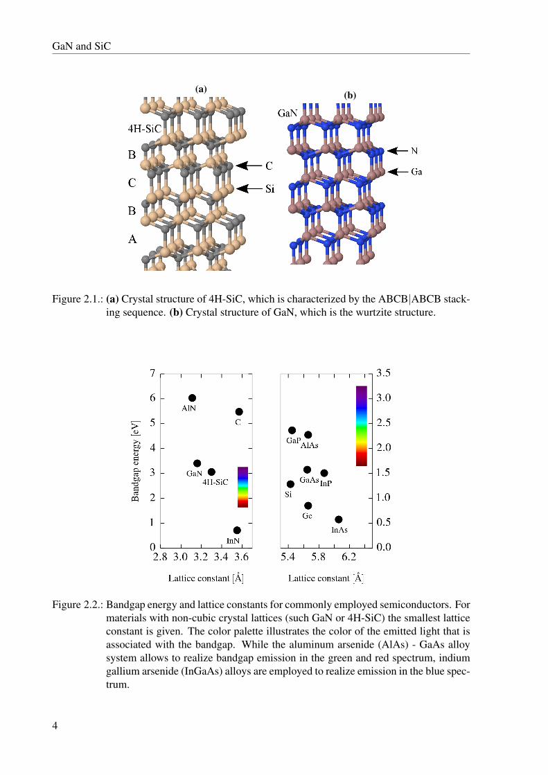
SiC The compound semiconductor SiC has been found to crystallize in a variety of structures,which are commonly referred to as polytypes. The main crystallographic building blocks are thetetrahedral bonds of the tetravalent Si and carbon (C) atoms. A polytype is characterized by astacking sequence, which is given by the variation of the occupied lattice sites along the c-axis.More than 200 polytypes have been found, with the most important being the cubic 3C-SiC andthe hexagonal 4H-SiC and 6H-SiC. Figure 2.1a shows the crystal structure of 4H-SiC with itscharacteristic ABCB|ABCB stacking sequence.
Even though all polytypes are characterized by a strong Si-C bond, the physical propertiesstrongly differ between various polytypes. Due to its high electron mobility the 4H-SiC is themost commonly used for electronics applications. 6H-SiC has been thoroughly studied as well,however, the electron mobility is inferior to 4H-SiC. 4H-SiC exhibits a wide-bandgap (3.26eV),which is indirect (as is the case for all polytypes). Figure 2.2 visualizes the bandgap and latticeconstants for several commonly used semiconductors for comparison. The melting point isan excellent measure for the high temperature capabilities of a material and 4H-SiC’s meltingpoint is exceptionally high (≈ 2800C) [2], which is linked to the high binding energies2. Forpower electronics the thermal conductivity and the critical field strength are vital. 4H-SiC showsexcellent values with 5Wcm-1K-1 and 3.5MVcm-1, respectively [2].
1White light sources can be realized by exiting a yellow phosphor with blue light emitted by GaN-based LEDs.The yellow phosphor emits light with a broad spectrum, which is perceived as white by the human eye [4].
2The melting point for Si is 1414 C.
3
GaN and SiC
(a) (b)
Figure 2.1.: (a) Crystal structure of 4H-SiC, which is characterized by the ABCB|ABCB stack-ing sequence. (b) Crystal structure of GaN, which is the wurtzite structure.
Figure 2.2.: Bandgap energy and lattice constants for commonly employed semiconductors. Formaterials with non-cubic crystal lattices (such GaN or 4H-SiC) the smallest latticeconstant is given. The color palette illustrates the color of the emitted light that isassociated with the bandgap. While the aluminum arsenide (AlAs) - GaAs alloysystem allows to realize bandgap emission in the green and red spectrum, indiumgallium arsenide (InGaAs) alloys are employed to realize emission in the blue spec-trum.
4

GaN and SiC
GaN GaN crystallizes in the wurtzite structure, which is based on a hexagonal lattice. Fig-ure 2.1b illustrates that the crystal structure is non-centrosymmetric and inherently polarizeddue to the net separation of the Ga3+ and N− ions [5]. The non-centrosymmetric latticecauses polarization effects in GaN. Spontaneous polarization is observed along the c-axis ofthe Wurtzite structure, which causes a strong electric field. Additionally, piezoelectric polariza-tion with piezoelectric constants that are ten-times higher than any other III-V semiconductorshas been observed[6]–[8].
GaN’s bandgap at room temperature is 3.4eV, which is three times higher than for Si (1.1eV).Like all III-N semiconductors, GaN is characterized by a direct bandgap, allowing highly ef-ficient electron-photon interaction [9]. The melting point is nearly as high as for SiC with2500C [10]. For GaN a critical field strength of 3.3MVcm-1 is observed, however, the thermalconductivity is significantly lower than for 4H-SiC (1.3Wcm-1K-1) [3].
Figure 2.3 summarizes GaN’s and 4H-SiC’s material properties in comparison to other semi-conductors, i.e., Si and gallium arsenide (GaAs), corroborating that both semiconductors, GaNand 4H-SiC, are excellently suited for application in power electronics. However, in order toexploit their full potential, well-controlled and optimized fabrication processes are required.In the following section the significant processing challenges for both semiconductors are dis-cussed.
Figure 2.3.: Comparison of the material properties of Si, GaN, GaAs, 4H-SiC and 6H-SiC.
5
GaN and SiC
2.2. Fabrication
2.2.1. Substrate and Thin Film Fabrication
Every semiconductor device concept relies on high substrate and thin film quality, because effi-cient electronic transport is only possible in nearly perfect crystalline structures with low defectconcentrations. From a historical point of view, breakthroughs in this field are indispensable forevery semiconductor material system.
SiC substrates are fabricated using the Levy or seeded sublimation process. Both require seedsthat originate the Acheson Process. Although the process was, in principle, functional in the1970s, the defect density in the resulting substrates were problematic. The most famous ex-tended defect is the SiC micro-pipe, which is a screw dislocation that propagates through theentire bulk. This potentially device-killing defect could be eliminated and is no longer a majorconcern. On the contrary, thin films can be deposited using high temperature chemical vapordeposition with process temperatures around 1600C [2].
Due to the fact that a process similar to the Czochralski growth for Si does not exist, GaN sub-strates are fabricated on top of foreign substrates (Si, sapphire). Commonly employed methodsare hybrid vapor phase epitaxy (HVPE) and ammonothermal growth [11]–[13]. Compared tothe well controlled Si substrates, GaN substrates exhibit a higher defect density and are moreprone to contain extended defects, which severely reduce the device quality. The develop-ment of metalorganic vapor phase epitaxy (MOCVD) for the controlled fabrication of epitaxialGaN films by Akasaki and Amano [14] revolutionized GaN process technology, which cul-minated in the demonstration of the first GaN-based blue LED. Even though molecular beamepitaxy (MBE) can be alternatively used, MOCVD is still the standard thin film fabricationtechnique [3].
A special thin film fabrication technique is thermal oxidation, where the semiconductor is chem-ically modified near the surface. The resulting semiconductor-insulator interfaces are essentialfor device isolation, passivation, and gate oxide formation in metal-oxide-semiconductor fieldeffect transistors (MOSFETs). 4H-SiC is particularly attractive regarding oxidation, as it al-lows for naturally growing silicon dioxide (SiO2) - as with Si. The chemical reaction proceedsaccording to [15] (dry oxidation)
SiC+32
O2 SiO2 +CO. (2.1)
The native SiO2 allows to achieve quality semiconductor-oxide interfaces with the interfacestate densities in the order of 1012 cm−2eV−1, which is significantly higher than for modernSi-SiO2 interfaces, where values around 1010 cm−2eV−1 are typically not exceeded [16]–[18].Having SiO2 as native oxide, SiC technology strongly benefits from the highly stable and ex-tensively investigated oxide [19].
Oxidation of GaN is more involved. In an oxygen (O) rich atmosphere the off-stoichiometricnative gallium oxide GaOx is formed,
GaN+O2 GaOx +NOx. (2.2)
6

GaN and SiC
Even though thin films have been recently successfully oxidized [20], thick thermal oxides(≈ 100nm) exhibit poor surface quality. Therefore, dielectric films (e.g., silicon oxide, siliconnitride or aluminum oxide) are preferentially deposited on GaN substrates.
A high quality substrate and precisely controlled thin film deposition/growth allows to define thesemiconductor device geometry by additive processes. However, sophisticated device structuresrequire subtractive processes as well. This is realized by the etching processes discussed in thenext section.
2.2.2. Etching
In order to fabricate complex device geometries by a subtractive process, a precise control ofetching technology is required. Even though wet chemical etching is possible for GaN and SiC,dry etching is better suited for industrial applications [5]. In particular, reactive-ion etching(RIE) techniques that operate with chlorine compounds are important. However, RIE typicallyinduces lattice defects and disorder, which can be minimized by optimizing the etching pro-cess parameters. In particular, for GaN there is still room for improvement regarding plasmacomposition [2], [21], [22].
With thin film fabrication and etching techniques complex device geometries can be realized.However, to engineer particular electrical properties, impurities are deliberately introduced intothe semiconductor. This process is called doping and is discussed in the following.
2.2.3. Doping
The basic building blocks of every electronic device are pn-junctions [23], which allow to con-trol the electronic transport. Consequently, well-defined n- and/or p-doped regions are required.Si can be doped during growth (in situ doping), by diffusion of impurities or via ion implan-tation. Both 4H-SiC and GaN are characterized by small diffusion coefficients of the commonimpurity species, resulting in negligible impurity diffusion3. Consequently, doping by diffusionis not feasible for these materials.
Two alternatives have been established, in situ doping and ion implantation. In situ doping isessentially a modification of the thin film fabrication step. By intentionally adding impuritiesto the growth atmosphere, the doping concentration of the thin film can be precisely controlled.In order to fabricate deep doping profiles and sophisticated vertical device structures, ion im-plantation is required. Impurity ions are extracted from a gaseous source and electrostaticallyaccelerated to high energies (keV). Subsequently, the ions are injected into the target material(e.g. GaN-substrate), where they are slowed down by nuclear and electronic scattering. An im-portant side effect of the high energy implantation is that the host atoms are displaced, leadingto severe lattice disorder, which is further discussed in Section 3.1.
3The diffusion coefficients of all relevant impurities in GaN are below 2×10⁻¹³ cm2s−1 at 1400 C [24]. For SiCthe coefficients are even smaller for 1700 C [2].
7

GaN and SiC
SiC By implanting phosphorus (P) or nitrogen (N) n-doped SiC can be achieved. Aluminum(Al) and boron (B) are used for p-type doping. Ion implantation technology for 4H-SiC hasmatured to the point that the implanted profiles can be precisely controlled. However, it hasbeen observed that high dose implantation (> 1015 cm−2) is more efficient if the implantationsare performed at elevated temperatures (1500C). Due to the enhanced thermal energy theannealing process already starts during the implantation process. This phenomenon is referredto as in situ annealing [25]. Due to its small atomic radius, implanted B (in 4H-SiC) shows somepeculiarities. E.g., high ionization energy (350meV) and out diffusion during hot implantationhave been observed [2].
GaN Like all III-N materials, GaN is characterized by larger binding energies and smallerinter-atomic distances than Si. Therefore, it is more difficult to incorporate substitutional im-purities. Furthermore, there is a high threshold for damage accumulation, which makes GaNhighly difficult to amorphize. The physical reason is the high ionicity of the Ga-N bond. Donorincorporation of Si with maximum concentrations exceeding 1020 cm-3 has been demonstrated.Alternatively, oxygen (O) also serves as donor impurity. The most commonly used acceptorimpurity is magnesium (Mg) [5], [9], [10], [24], [26], [27].
The implantation process is complicated because as-grown GaN has been found to exhibit n-type background doping with an effective donor concentration of ND = 1016 cm-3 [9]. Thephysical reason has been controversially discussed throughout the 1990s and early 2000s. Eventhough some experimental studies were indicating that N vacancies play a role, it has recentlybeen concluded that O is unintentionally incorporated during growth contamination [28], [29].Furthermore, magnesium-hydrogen (Mg-H) complexes play a decisive role in the unintentionaldopant passivation of Mg-doped GaN [30].
Ion bombardment induces lattice damage that always requires an annealing step following ionimplantation. In the next section annealing is discussed from a process technology point ofview. The physical mechanisms are further examined in Chapter 3.
2.2.4. Annealing
In order to recover from the lattice damage caused by ion implantation, energy must be intro-duced into the host crystal. Usually, thermal energy is used, which is practically achieved byheating the implanted crystal to elevated temperatures (thermal annealing). Even though alter-native anneal technologies like low energy electron beam irradiation (LEEBI) can be employedas well [31], [32], thermal annealing is the standard process.
The annealing temperatures that are required to successfully activate implanted impurities de-pend on the atomic binding energies and thus are related to the melting temperatures. It hasbeen empirically determined that 2/3 of the melting temperature results in high activation ofdopants [24]. For 4H-SiC and GaN this amounts to approximately 1850C and 1650C, re-spectively, which are both extremely high and present considerable technological challenges.The annealing equipment, the substrate, and the sample are required to endure those tempera-tures. A rapid thermal annealing (RTA) setup, which consists of halogen lamps and reflectingcavities, allows to precisely control the temperature ramps. The most critical task is accuratetemperature measurement, which is performed with pyrometers [33].
8

GaN and SiC
SiC For 4H-SiC substrates Si desorption from the surface and migration of surface atomsresults in high surface roughnesses. These detrimental effects can be reduced by depositing acap layer on top of the substrate. In particular, carbon caps, which are usually deposited withradio frequency sputtering, have proven successful. After the annealing step the cap can besmoothly removed by oxygen plasma etching resulting in high quality surfaces [2].
GaN The annealing process of implanted GaN is significantly more challenging. Indepen-dent of doping concentration, the substrate surface starts to severely decompose at 840C foratmospheric pressures. N atoms are lost by forming gaseous N2. Additionally, Ga droplets areleft behind on the surface. This process is thermally activated, which causes the reaction ratesto strongly increase for higher anneal temperatures, rendering thermal annealing steps withoutfurther precautions close to impossible [10]. Similar to SiC, capping layers have been observedto successfully avoid surface decomposition. Before thermal annealing a AlN, SiO2 or SiNlayer, which protects the surface, is deposited. After annealing, the cap is removed to allowfurther device processing [34], [35]. Figure 2.4 illustrates the typical process sequence.
GaN Substrate
GaN Epilayer
Implanted
(a)
GaN Substrate
GaN Epilayer
Implanted
Cap
(b)
GaN Substrate
GaN Epilayer
Active GaN
(c)
Figure 2.4.: Typical process sequence to protect a GaN sample’s surface during the high-temperature annealing step. (a) The dopants are implanted into the epitaxial layer.(b) A cap layer (such as SiO2 or AlN) is deposited and the thermal annealing stepis performed. (c) After thermal annealing the implanted dopants are electricallyactive and the cap is removed.
The capping technology has been effectively employed to achieve a high activation efficiencyin Si-implanted GaN. Annealing temperatures in the range from 1200C to 1350C have beenrealized. Strikingly, a reduced activation efficiency for low (≈ 1017 cm−3) and moderate (≈1018 cm−3) doping concentrations has been observed [36]–[38], which is in contrast to the fullactivation that is typically achieved in SiC (as discussed in Section 4.3). This phenomenon hasbeen attributed to compensation by unintentionally introduced elements such as carbon, but isstill controversially discussed in the literature [28], [38], [39].
Activation of Mg-implanted GaN (forming p-type regions) is more difficult than Si-implantedGaN. On the one hand, this is caused by background doping, which has to be compensated andthus requires enhanced acceptor concentrations. On the other hand, it has been observed thatannealing temperatures above 1350C are necessary [40]. This is linked to the formation ofMg-H complexes that do not contribute electrons to the conduction current [41]–[43]. In order
9
GaN and SiC
to enhance the activation efficiency, RTA procedures have been investigated, which involve two-step annealing [44] and multicycle RTA [35], [40], [45]. The fabrication techniques discussed inthe previous sections provide tools to realize sophisticated semiconductor devices based on GaNand 4H-SiC. In the following, the applicability of these semiconductors for power electronicsis assessed with figure of merits and characteristic device structures are discussed.
2.3. Applications
In this section a selection of the most relevant device concepts that are based on 4H-SiC or GaNare presented. In power electronics, electric power is converted using electronic circuits. Therange of applications compromises AC-DC converters, automobile electronics, power supplyunits, factory automation, and power transmission. The growing market of electric vehiclesadditionally reinforces the need for efficient power conversion technologies. In Si-based powerdevices conversion efficiency is limited to approximately 90%, with the rest dissipating as heat,corroborating the need for an improved technology [2].
Power device structures are preferentially manufactured with a vertical device structure. Thisallows to place one terminal on the opposite side of the chip and thus enabling uniform currentdensities and high total currents [46]. In order to assess and optimize device performance figureof merits are employed. These are typically either highly significant device parameters, such asblocking voltage and on-state resistance or derived quantities. Baliga [47] introduced a derivedquantity, which characterizes the influence of the material properties on the crucial on-stateresistance that is associated with vertical devices. The ideal specific on-state resistance is givenby
Ron =4V 2
BεsµnE3
c=
4V 2B
BFOM, (2.3)
where VB is the breakdown voltage, εs is the semiconductor’s permittivity, µn is the bulk electronmobility, and Ec is the critical electric field associated with avalanche breakdown at the blockinginterface (metal-semiconductor interface or pn-junction). The denominator BFOM = εsµnE3
c iscommonly referred to as Baliga’s figure of merit (BFOM). A semiconductor material is consid-ered well suited for vertical power devices if the on-state resistance is small, or equivalently,BFOM is high. The relation between the BFOM calculated by Baliga for GaN, 4H-SiC, and Siis [47]
BFOMGaN ≈ 0.5 ·BFOM4H-SiC ≈ 5×10⁻⁴ ·BFOMSi. (2.4)
The high values for GaN and 4H-SiC indicate the exceptional potential of these semiconductorsto drastically improve the performance of Si-based power devices. Two typical vertical powerdevice structures are the double-implanted MOSFET (DMOSFFET, shown in Figure 5.1) andthe junction barrier Schottky (JBS) rectifier (Figure 5.7), which are both further examined inChapter 5.
Apart from vertical power devices, the polarization properties of GaN allow to design highperformance lateral device structures. The high electron mobility transistor (HEMT), whichis characterized by a two-dimensional (2D) electron gas layer, allows to increase the electron
10

GaN and SiC
(a)
i-GaN
i-AlGaN
p-GaNS DG
(b)
Sapphire
GaN Buffer
n-GaN n-Electrode
n-AlGaNn-InGaNInGaN
p-AlGaNp-GaN
p-Electrode
Figure 2.5.: (a) GaN HEMT that is based on lateral current flow [3]. S refers to the source, G tothe gate, and D to the drain contact. The prefix i refers to intrinsic and p to p-dopedregions. High electron mobilities are achieved by exploiting the GaN’s inherentpolarization at the GaN-AlGaN hetero-junction. (b) Schematic GaN vertical LEDstructure. The AlGaN and InGaN alloys can be precisely engineered to enable lightemission in the UV and blue range of the spectrum. In order to grow a GaN epilayeron the sapphire substrate, an auxillary buffer layer is deposited.
mobility to values above the bulk mobility. With high electron mobility a high switching speedcan achieved, making the structure ideally suited for high frequency applications. GaN’s in-herent polarization allows to form the 2D electron gas layer without resorting to additionalspacer layers, which are necessary for GaAs-based HEMTs (Figure 2.5a). Lateral devices relyon heterojunctions (i.e., junctions between semiconductor with dissimilar lattice constants andbandgaps) between GaN and the alloy aluminum gallium nitride (AlGaN). The active region ofa lateral devices is close to the surface, which imposes less rigorous demands on the bulk crystalquality. Due to the high defect concentrations in GaN substrates, HEMTs were demonstratedearlier than vertical devices [3], [48].
A wide-bandgap semiconductor can also be applied in the field of optoelectronics and photonics.With 3.4eV and 3.26eV bandgaps for GaN and 4H-SiC, respectively, light generation anddetection in the ultraviolet (UV) part of the electromagnetic spectrum is possible. 4H-SiC-basedUV photodetectors have been successfully realized [49]. Despite having an indirect bandgap,SiC-based LEDs are commercially available, however, GaN’s direct bandgap allows to realizeconsiderably more efficient LEDs for wavelength near the visible spectrum. The demonstrationof the first commercially available blue LED by Nakamura et al. in 1994 [50] marked animportant milestone for the GaN technology. Figure 2.5b schematically shows a LED devicestructure, which uses the aluminum concentration in the AlGaN alloys to control the spectrumof the emitted light. The realization of blue GaN-based LEDs laid the foundation for efficientwhite light sources and was only possible with the progresses in thin film deposition (MOCVD)and Mg activation technology, spearheaded by Akasaki et al. [32]. In 2014, the Nobel Prize inphysics was awarded to I. Akasaki, H. Amano and S. Nakamura for efficient blue light-emittingdiodes leading to bright and energy-saving white light sources [51].
11


3. Physical Mechanisms of Annealing
Thermal annealing is an important technological process step in semiconductor technology.Originating from metallurgy the term thermal annealing refers to the process of heating a ma-terial above the recrystallization temperature and subsequently cooling it down at a slow rate.Heating above recrystallization temperature allows to decrease defect concentrations and stressin the material’s lattice [52]. In general, the atomic configuration in a crystal is continuouslyrearranging if additional energy is added to the system.
Thermal annealing is crucial for the doping of semiconductors by means of ion implantation.Due to multiple collisions the ion bombardment causes disarray in the former single crystal. Aplethora of defects, most prominently point defects, is formed and referred to as implantationdamage. Most importantly, the accumulated defects do not allow the introduced dopants tocontribute to the electric properties of the semiconductor, which are desired to be precisely con-trolled by doping. As a consequence, thermal annealing after implantation is required. In thischapter the nature of the lattice damage induced by ion implantation and the physical processesleading to electrical activation are discussed.
3.1. Ion Implantation Induced Damage
When discussing the doping of semiconductors, it is of utmost importance to differentiate be-tween the chemical concentration of dopants Cx and the electrically active concentration Ca.The former essentially counts the number of incorporated impurity atoms (e.g. Mg in GaN orAl in SiC) in a unit volume. In order to contribute to the electric properties, the impurity atomsare required to be ionized. However, this is only possible if the impurity occupies a latticesite. In order to achieve the situation of full electrical activation, where every implanted atomcontributes to conductivity, the impurity atoms have to occupy lattice site and thus replace hostatoms. An ideal replacement is not possible in a real system. Therefore, the achievable activedonor or acceptor concentrations are limited.
3.1.1. Activation Limiting Factors
For every solid material there is a solubility limit, which is also referred to as solid solubility.This is the maximum concentration that the impurity can attain in the semiconductor (in thermalequilibrium). If the solubility limit is exceeded, agglomerates and clusters of impurity atomsare formed. In the case of high impurity concentrations it is energetically more favorable for theindividual impurity atoms to form bonds to each other than to host atoms. As a consequence, atwo phase system is emerging and the electrical activation saturates [42], [53].
13

Physical Mechanisms of Annealing
Even if the impurity concentration is considerably below solid solubility the incorporation ofimpurities in configurations other than host lattice site replacements can have detrimental effectson electrical activation. Impurity atoms can occupy interstitial lattice sites or cause vacanciesgenerated by the ion bombardment. In compound semiconductors like SiC and GaN antisitedefects (e.g., N atom on Ga site in GaN) are of importance as well. Additionally, native pointdefects in the host crystal like self-interstitials can lead to deactivation by means of compensa-tion. Figure 3.1 sketches the common point defects. Figure 3.2 visualizes the lattice damagethat is induced by implanted Al in 4H-SiC. Point defects affect the quality of the doped layers,e.g., Ga vacancies have been identified as effective acceptors, which compensate n-type dop-ing. Furthermore, impurity species can be unintentionally introduced during the implantationprocess. In GaN the compensation of p-type doping through incorporation of O during Mgimplantation has been studied thoroughly [28], [29], [42].
VSI
SII
Figure 3.1.: Illustration of the fundamental point defects, i.e., interstitial impurity (II), substitu-tional impurity (S), native vacancy (V) and self-interstitial (SI). The host atoms arerepresented by the blue and impurity atoms by the orange circles.
In order to fully understand the doping process, the species contributing to the net doping have tobe investigated. Typically, a combination of experimental characterization techniques and the-oretical calculations is employed to examine the micro-physical impact of native and impurity-related defects. This is illustrated in the next section in an exemplary way for GaN.
3.1.2. Impurities and Defects in GaN
In Chapter 2 the challenges of achieving high activation ratios in GaN have been highlighted.The reasons for those difficulties are controversially discussed in the literature: Experimentaland theoretical studies were conducted improving the understanding of the atomic configurationof doped GaN [9], [42], [55]–[58]. In this section the most important point defects in GaN are
14
Physical Mechanisms of Annealing
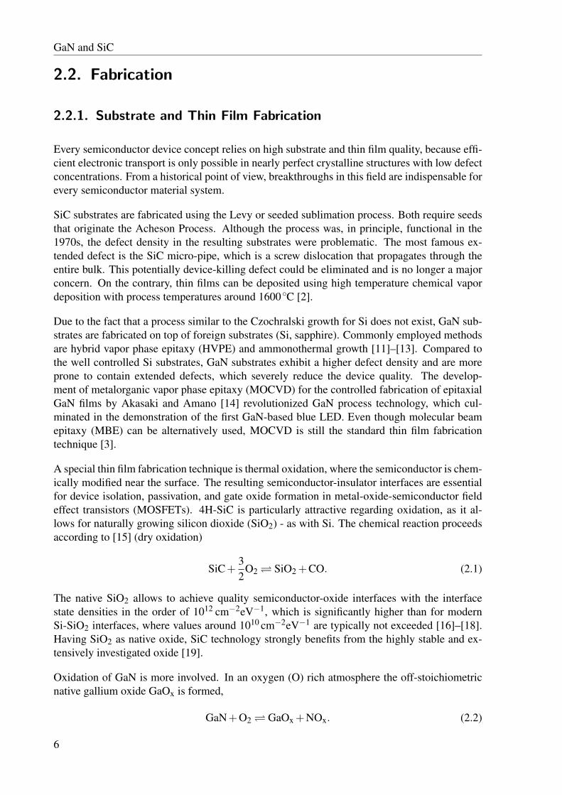
(a) (b)
Figure 3.2.: Visualization of the implantation damage in 4H-SiC. (a) A perfect 4H-SiC-crystalis shown, based on a molucular dynamics simulation (large-scale atomic/molecularmassively parallel simulator, LAMMPS [54]). (b) An impurity atom (Al, red) isimplanted into the crystal and induces lattice damage.
presented in order to illustrate the typical implantation induced crystal damage in compoundsemiconductors.
Even though implantation damage is usually associated with deviating atomic configurationsinvolving impurity atoms, the recoil cascade initiated by the ion bombardment leads to na-tive point defects as well. Ga or N atoms can be pushed away from their favored lattice sitesand eventually occupy a (meta)-stable position in between. This configuration is called self-interstitial and for the compound semiconductor GaN there are the Ga and the N self-interstitials(Gai and Ni). A Ga atom can also occupy a N site and vice versa (antisite defects - GaN, NGa).Additionally, a Ga or a N atom can leave its original, immediate surroundings and leave itslattice site behind empty, which is referred to as vacancy (VGa, VN) [29].
Experimental investigations show that the typical concentrations of the different defect typesstrongly differ. Vacancies are present in significant concentrations even in bulk GaN, whereasantisite defects are rare. The probability of forming a certain defect type depends on the asso-ciated energy barriers which have to be overcome in order to change the atomic configuration.In theoretical studies the concept of formation energy Ef
D is used to quantify the energy bar-rier. Usually density function theory (DFT) calculations are employed to determine formationenergies.
The N vacancy VN came to prominence because it was regarded as being the main reason forthe difficult p-type doping. Theoretical studies show that VN acts as a shallow donor in GaN.Therefore, the intended p-type doping is compensated by the vacancies. The formation energyof N vacancies is usually high, indicating only minor concentrations in the crystal. However,in p-type GaN the formation energy is significantly smaller, which results in increased creationrates of N vacancies. The counterpart, the Ga vacancy VGa is responsible for yellow lumi-nescence in GaN. Even though GaN’s bandgap suggests photon emission in the UV, the Ga
15

Physical Mechanisms of Annealing
vacancy introduces additional states allowing optical transitions around 2.1eV [29], [42], [57],[59].
The self-interstitials Ni and Gai together with the antisite defects NGa and GaN are characterizedby a significantly higher formation energy, which is caused by the strong distortion in the lattice.Nevertheless, depending on the position of the Fermi level these defects may act as acceptorsor donors (amphoteric defects), which adds a further degree of complication, especially in hightemperature conditions [42].
Donor incorporation in GaN has been successfully achieved using ion implantation of silicon.Due to the similar atomic radius, the Ga site is favorable for a Si atom (SiGa). On the con-trary, the N site (and additionally the N interstitial configuration) are energetically unfavorable.Therefore, it is very likely that implanted Si atoms are incorporated at the desired lattice site.There are, however, further elements that lead to unintentional incorporation of donors. O hasbeen established as being the main reason for the unintentional n-type conductivity in GaNdiscussed in Section 2.2.3. A potentially amphoteric dopant is C. Its significance was contro-versially discussed in the 1990s [60], but more recent investigations showed very high formationenergies for C impurities [29], [42].
The most scientifically involved and historically impactful point defect is the Mg impurity inGaN. Mg is favorably incorporated at Ga sites MgGa. The formation energy is low enough toenable large active Mg concentrations in GaN with the help of annealing techniques like low en-ergy electron beam irradiation (LEEBI) or thermal annealing. However, the ionization energy ishigh (200 meV) and the Mg atoms form agglomerates with N atoms (e.g. Mg3N2) affecting thesolubility limit of Mg in GaN. Additionally, a strong compensation mechanisms was observedexperimentally and linked to H complexes. The reduction of the concentration of compensatedacceptors using LEEBI (Nakamura et al. [61]) was one of the significant breakthroughs enablingblue GaN-based LEDs [29], [42], [59].
The point defects discussed in this section can potentially all exist after an implantation step.Having described the variety of implantation-induced defects, the influence of thermal anneal-ing has to be considered.
3.2. Thermal Annealing
Figure 3.3 illustrates the situation after ion implantation from an abstract point of view. Imme-diately after (or during the ongoing) implantation the (crystal-) system is in a non-equilibriumstate. The atoms (both host and impurity atoms) immediately react and relax towards a localminimum in energy, which is referred to as in situ lattice recovery. The relaxation process typ-ically takes place at very short time scales. This phenomenon is of importance for SiC, whereimplantation at elevated temperature improves the final electrical activation [2].
However, in situ lattice damage recovery is typically limited by energy barriers which preventthe atoms from further reconfiguration. In order to overcome these energy barriers, additionalenergy can be added to system in the form of heat (e.g., thermal annealing). At higher tem-peratures the higher vibrational energy enables more elaborate reconfiguration. The essentialdifference compared to the in situ recovery process is the time scale of the reconfiguration.
16

Physical Mechanisms of Annealing
These are typically in the seconds and minutes regime (for 4H-SiC even in the hours regime forhigh doping concentrations > 1019 cm−3 [62]) and define the required annealing times.
The atomic reconfiguration that takes place during the annealing step is a short range reconfigu-ration. This is in contrast to the diffusion process, which is characterized by atomistic transportover longer ranges. Nevertheless, the elevated temperature during thermal annealing magnifiesthe diffusion coefficients as well. In particular, the impurity diffusivity has to be taken into ac-count. Arsenic (As) diffusion is of importance, because the associated diffusivity is high, whichleads to a broadening of the implantation profile [63]. For GaN and SiC diffusion of impurityduring thermal annealing is a minor issue. Except for implanted B in SiC, the diffusivity can beusually neglected.
Reaction coordinate
Tota
lene
rgy
a
b
c
d
In siturelaxation
Thermal annealing
Activation barrier
Figure 3.3.: Schematic illustration of the thermal annealing process. The implantation processinduces an energetically non-favorable state (a). The system (i.e., host crystal andimplanted impurities) immediately relaxes to a state that is stable in equilibrium (b).However, this state is characterized by poor electrical activation. More elaborateatomic reconfiguation is necessary to overcome the activation barrier (c). Sub-sequent relaxation to an energy minimum (d), which is associated with eloborateelectrical activation.
A related issue is impurity cluster formation and growth for high implantation doses leadingto over-saturated or amorphous region (precipitates). Due to their complexity a comprehensivephysical description is difficult. However, they are highly significant, because their presencestrongly deteriorates semiconductor device performance [38], [63]. The next section deals withapproaches to understand the micro-physical processes that proceed during annealing steps.
3.3. Approaches to Physical Modeling
In Section 3.1.2 and Section 3.2 the mechanisms of lattice damage and thermal annealing arediscussed in a very general and abstract way. In order to gain further insight into the processesrelated to implantation and electrical (de-)activation, it is beneficial to employ methods from
17

Physical Mechanisms of Annealing
thermodynamics and physical chemistry. In this section approaches to physical modeling aresummarized. Similar techniques have been successfully employed for modeling As diffusionand activation in Si [63].
3.3.1. Point Defect Reaction Equations
The key idea is to break the complex atomic reconfiguration down into simple reaction equa-tions describing the conversions between different types of point defects. In other words, thereaction equations allow to characterize the sources and sinks of point defects in the lattice. Inthe following, an elemental semiconductor is assumed, i.e, there is only one type of vacancy andinterstitial. This assumption facilitates the formulation of reaction equations but can be straight-forwardly generalized for compound semiconductors. A vacancy V can form a dopant-vacancypair AV with a substitutional impurity atom A. The corresponding reaction equation is
A+V AV, (3.1)
indicating the dynamic equilibrium between the individual defects and the dopant-vacancy pair.A dopant-vacancy pair can be regarded as physical entity. A similar case is the interstitialmechanism (also called kick-out reaction I)
A+ I AI, (3.2)
which involves an interstitial A and a dopant-interstitial pair AI. A dopant atom can also occupyan interstitial lattice site Ai, which is described by the substitutional interchange mechanism(kick-out reaction II)
A+ I Ai. (3.3)
Likewise, it is possible that the impurity atom ’jumps’ to a vacancy (Frank-Turnbull mechanism)
A Ai +V. (3.4)
Furthermore, host atoms can spontaneously move from a lattice site to an interstitial site leavinga vacancy behind (Frenkel mechanism)
I+V 0. (3.5)
In Section 3.1.2 the importance of point defect cluster formation is highlighted. An interstitialcluster can be modeled by
In + I In+1 (3.6)
and the recombination of cluster with vacancies by
I+V 0, In+1 +V In. (3.7)
The reactions given above express the transition between the different neutral defect states.However, point defects can assume a charged state as well, which is of special importance for theannealing process. Due to the additional Coulomb forces, the interaction with the surroundingatomic configuration is significantly influenced. Having to describe the exact charge state is a
18

Physical Mechanisms of Annealing
major complication and the involved configurations depend heavily on the considered material.To give one example, the vacancy mechanism involving charged species can be described with
Ai +V j (AV)i+ j, (3.8)
where i, j ∈ . . . ,−1,0,1, . . . refers to the charge state of the subsitutional impurity and thevacancy, respectively. During ion implantation bulk atoms are knocked off the lattice sites, thusinterstitials and vacancies are created. However, this process is not an equilibrium process,which requires the Frenkel formulation (3.5) to be adapted
0→ I+V. (3.9)
Additionally, the knocked-off atoms usually have enough energy to create a collision cascadeand a multitude of interstitials and vacancy pairs is created. Being a non-equilibrium process,simplifying assumptions are required to be able to describe ion implantation damage withinthe framework of equilibrium reactions. It is commonly assumed that a perfect annealing step,which leaves only one additional interstitial (i.e, the host atom that is pushed off its lattice site)per dopant behind. For implantation with a concentration of N, the equilibrium state is modeledby [63], [64]
num(I)−num(V) = N, (3.10)
where num refers to the number of interstitals or vacancies.
The reaction equations describe the transition between different potentially charged defectstates. However a full description of physical state requires information about the concen-tration of the point defects. Statistical mechanics can provide this as it is discussed in the nextsection.
3.3.2. Equilibrium Concentration Modeling
When a system is considered at temperatures T above 0 K statistical mechanics predicts that acertain concentration of point defects exists in (quasi-) equilibrium. The native point defect con-centration CD depends on the formation energy Ef
D for a generic defect D and the concentrationof available lattice sites Cs
CD
Cs= θD exp
(−
EfD
kBT
), (3.11)
where θX is the number of degrees of internal freedom of the defects on lattice sites (spinor orientation degeneracy) and kB is the Boltzmann constant. The formation energy can bedetermined by resorting to ab-initio calculations (DFT, see also Section 3.1.2) or measurementtechniques like positron annihilation or deep-level transient spectroscopy [64].
Having the concentration of neutral defects established, the concept of equilibrium coefficientsK can be employed to determine the concentration of charged defects. Assuming Maxwell-Boltzmann statistics and relatively small defect concentrations (CDCs, dilute concentration
19

Physical Mechanisms of Annealing
approximation) the theory developed for neutral defects can be extended to describe chargeddefect configurations,
CiD = KDiC0
D(ni/n)i (3.12)
where CiD is the concentration of the generic point defect D in charge state i, KDi is the reaction
coefficient and C0D is the concentration of the neutral charge state1. The equilibrium theory can
be employed because the electric charging processes are very fast and can be assumed to occurin quasi-equilibrium [63].
For impurity related defects, generically referred to as AD, (3.11) and (3.12) can be adaptedto
CAD = θADCA ·CD
Csexp(
EfAD
kBT
)(3.13)
and
C(AX)i = K(AX)iC(AX)0
(ni
n
)i. (3.14)
In order to determine the total concentration of charged defects (native and impurity-related)equilibrium equations have to be formulated for every defect type and eventually summedup [64].
With the steps discussed above the concentration of every point defect type is in principle de-scribed. However, it is important to account for the spatial distribution of point defects. Similarto lattice atoms, the thermal excitation causes on the macroscopic scale diffusive behavior ofthe defect, allowing to apply a continuum diffusion modeling approach, which can describe thespatial distribution and temporal progression of the point defects. This is of importance forimplantation damage and electrical activation modeling, because species redistribution and de-fect cluster formation can be described within a continuous framework, i.e., partial differentialequations.
3.3.3. Diffusion Modeling - Five Stream Model
Even if the diffusion coefficients of dopants are negligibly low (as it is the case for GaN and4H-SiC), the diffusion of native and impurity point defects affects the electrical activation pro-cesses. Point defect diffusion promotes the formation of clusters and is thus necessary to ac-count for. In the solid state the atoms are constricted to vibrations around their lattice site, whichhampers diffusion. However, in the presence of point defects, atoms can change its lattice site.Investigations of diffusion in Si crystals have shown that solid state diffusion is promoted byinterstitials and vacancies. From a macroscopic point of view, steep gradients in the concen-tration of the diffusing species are reduced with time. This is similar to the situation in fluids.However, the diffusion coefficient in the solid state are several orders of magnitude smaller than
1The factor ni/n follows the Maxwell-Boltzmann statistics nni= exp
(E0
f −E if
kBT
)[64].
20

Physical Mechanisms of Annealing
in fluids [65]. Nevertheless, a continuum modeling approach is usually employed. For everypoint defect D (including impurity atoms) a continuity equation of the form
∂CD
∂ t=−∇ · JD +GD, (3.15)
with the native point defect concentration CD, the flux of dopants/point defects JD, and a gen-eral generation term GD, is used. The continuity equations describe the temporal and spatialdevelopment of the defect and dopant concentrations. For an elemental semiconductor five con-tinuity equations have to be considered: For every dopant species three dopant related equations(A, AI, AV) and two native defect related equations (I, V). Thus, this model is referred to asFive Stream model. For compound semiconductor the different types of vacancies and intersti-tials (e.g. VGa, VN, Gai, Ni in GaN) have to be considered as well by an additional equation foreach type.
The total flux JD is composed of a diffusion and drift component. The former is promoted bygradients in the point defect concentration and assumes the form of Fick’s first law. The latteris only of importance for point defects in a charged state. An applied electric field leads to aspatial drift. Both components introduce parameters, the point defect related diffusion coeffi-cients, which are not directly measurable. Therefore, they have to be related to the macroscopic(measurable) diffusivities. The general generation term GD contains the information about thekinetics of point defect creation. Consequently, GD is determined by the concentrations of thereactants and products associated with the defect reaction equations given in Section 3.3.1 [63],[64], [66].
3.3.4. Elecrical Activation Modeling
The framework of the Five Stream model can be extended to account for electrical activation.From the variety of possible point defect reactions, the most important reactions that lead toelectrical activation have to be established. For As activation in Si the formation of AsV clustershas been experimentally attested to be responsible for reduced activation. For instance, Mg3N2clusters are associated with de-activation in GaN. Usually a multitude of cluster configurationsis found experimentally. With the help of ab-initio calculations (DFT and nudged elastic band)the most energetically favorable reactions can be determined. Nevertheless, the plethora ofpossible reactions drastically complicates the process. To give an example, in Si the As clusterequation
As4Si→ As4V+ I (3.16)
has proven successful. In order to account for a cluster’s impact on electrical activation therelease and emission of free electrons has to be modeled as well. For the considered examplethis leads to
(As4Si)4++4e− As4V0 + I0. (3.17)
Even with the essential mechanism established, the reaction equations and the Five StreamModel contain various coefficients. Their number can be reduced by expressing them in termsof the main quantities, namely defect concentration, equilibrium coefficients, carrier concentra-tions, macroscopic diffusion coefficients, and binding energies. Nevertheless, their values haveto be adapted in a fitting process to data from experiments. Figure 3.4 illustrates that the dis-cussed modeling approach has been successfully employed by Fastenko [63] to reproduce the
21

Physical Mechanisms of Annealing
measured saturation of electrical activation of As in silicon. While for dopant concentrationssmaller than approximately 5×1019 cm−3 full activation can be achieved employing high an-neal temperatures, the activation efficiency saturates for concentrations above this value. Thiscan be attributed to the intensified cluster formation for high dopant concentrations.
Figure 3.4.: Electrically active concentrations of As in Si as a function of the implanted concen-tration. The accurate simulation results that have been presented by Fastenko [63](solid lines) demonstrate that the approach to model electrical activation on thebasis of point defects is successful. Reproduced from [63].
3.3.5. Summary
The approaches of diffusion and (de)activation modeling of dopants, which have already beensuccessfully employed for As dopants in silicon, can be adapted to apply to other materials (suchas GaN) as well. The characterization of the point defects and associated reactions enables adeeper understanding of the underlying micro-physical effects that deteriorate electrical activa-tion. However, several challenges have to be overcome in order to formulate a comprehensivemodel allowing predictions about the activation state:
• Experimental characterization of native and dopant-related point defects.
• Experimental investigation of additional defects introduced by semiconductor processingsteps: chemical reactions (e.g. thermal oxidation) or ion-implantation (e.g., vacancy-typeclusters).
• Determination of energetically favorable defect configuration and reactions using ab-initio calculation (DFT) with a special attention to the charge state of defects.
22

Physical Mechanisms of Annealing
• Selection of the most important defect formation reactions based on the experimental andab-initio calculation input.
• Formulation of the (possibly extended) Five Stream model including all important defecttypes.
• Determination of coefficients and binding energies by fitting to experimental data. Thisrequires the availability of comprehensive experimental data for the considered dopantand host material, which includes diffusion-coefficients, active concentrations (transientand equilibrium values) and point defect reaction rates.
• (De-)activation modeling: Investigation of the mechanisms that limit electrical activation(e.g., clustering or compensation by unintentionally incorporated elements).
Even though a multitude of experimental studies have investigated defects in GaN and SiC,a fully physical activation model has not been developed. This can be partly attributed to thecomplexity that is induced by the presence of two type atoms in the respective lattices. The con-sequential variety of point defects presented in Section 3.1.2 gives rise to a plethora of possiblemicro-physical causes of reduced activation. However, further research is necessary to gain abetter understanding of the micro-physical mechanisms. In the next chapter, a semi-empiricalapproach to model the activation process, which captures the main macro-physical properties,but does not require full knowledge about the micro-physical processes is discussed.
23

4. Empirical Modeling of Annealing
The description of the processes during ion implantation and thermal annealing presented inChapter 3 allows for an understanding of the underlying mechanisms. Implantation processengineering is usually concerned with questions regarding process parameters like implanta-tion dose, annealing time, and annealing temperature. A fully calibrated physical model is inprinciple capable of delivering the required information to answer these questions, however,only at the cost of high computational effort. A different approach, which is being successfullyemployed in many fields of semiconductor technology simulation, is the empirical modelingapproach. This section highlights the general objective of the empirical method and discussesits application to model electrical activation of dopants in the wide-bandgap semiconductorsGaN and 4H-SiC. Phenomenological models that allow to optimize the fundamental processparameters associated with thermal annealing are derived from experimental data for a varietyof combinations of dopant atoms and host materials. Additionally, the relation between themodel parameters and the micro-physical processes are examined.
4.1. Objectives of Empirical Modeling
Empirical modeling focuses on the available experimental data and draws the attention to thefundamental idea of observing nature. The development of semiconductor process aims to op-timize the final device’s macroscopic behavior (i.e., current-voltage characteristics, breakdownvoltages, etc.) Therefore, it is a valid approach to abstract from the micro-physical complex-ity that is sketched in Chapter 3 and reduce everything to the macroscopic quantity electricalactivation ratio Ract, which describes the ratio between electrically active and total dopant con-centration. The main task is then to establish a functional relation (mathematical equation)between Ract and all relevant process parameters. This is most naturally accomplished by set-ting up experiments and vary the parameters of interest and determine the auxiliary coefficientsof the functional relation by fitting the coefficients to the experimental results.
The empirical approach offers only limited insights about the underlying physical processes.However, for device engineering this is not a major concern. The efficient calculation of etch-ing geometries, implantation profiles, and oxide thicknesses requires a mathematical descriptionof the considered material properties that should be as simple as possible to facilitate shortestpossible simulation times by simultaneously acceptable accuracy. Nevertheless, the parametersand coefficients appearing in the model equations can be related to physical quantities. Thesemi-empirical approach targets that issue by developing a greatly simplified physical model,which captures the essentials of the processes. The model predictions are subsequently com-pared to experimental observations and additional terms added to achieve suitable coincidence.An example from the area of oxidation is the Deal-Grove model, which describes the thermaloxidation kinetics of Si based on diffusion and reaction rates of the oxidizing species. However,
25
Empirical Modeling of Annealing
the Deal-Grove model does not satisfactorily describe oxide growth in the thin film regime,which led Massoud et al. to propose additional empirical terms [19], [67].
(Semi-) empirical models have the essential advantage that they provide the tools to optimizethe process parameters. Especially in the industrial environment a reduction of annealing time isbeneficial. With a well calibrated activation model the optimum combination of annealing timeand temperature, which allows reliable device operation, can be predicted. However, accuratecalibration is only possible if comprehensive experimental data is available. In the next sectionthe experimental findings for implanted SiC and GaN are reviewed.
4.2. Review of Experimental Findings
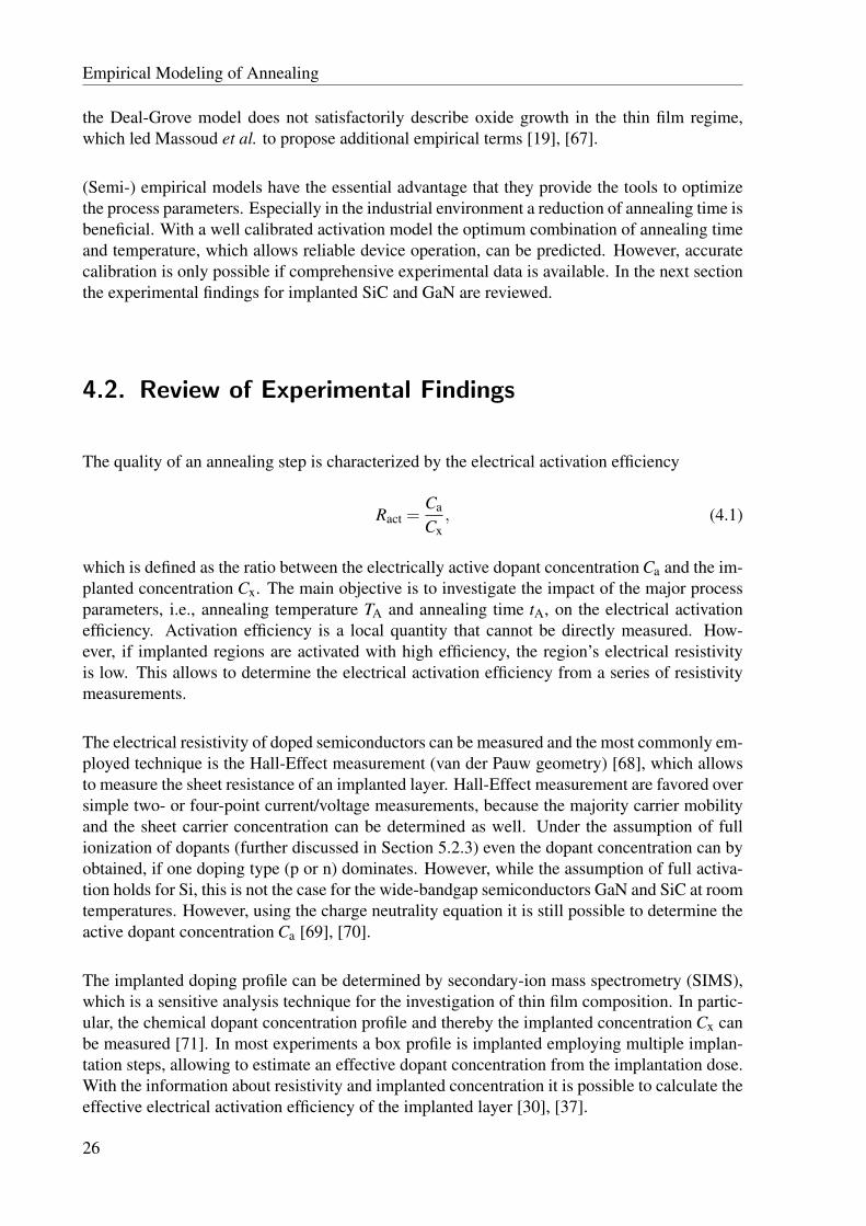
The quality of an annealing step is characterized by the electrical activation efficiency
Ract =Ca
Cx, (4.1)
which is defined as the ratio between the electrically active dopant concentration Ca and the im-planted concentration Cx. The main objective is to investigate the impact of the major processparameters, i.e., annealing temperature TA and annealing time tA, on the electrical activationefficiency. Activation efficiency is a local quantity that cannot be directly measured. How-ever, if implanted regions are activated with high efficiency, the region’s electrical resistivityis low. This allows to determine the electrical activation efficiency from a series of resistivitymeasurements.
The electrical resistivity of doped semiconductors can be measured and the most commonly em-ployed technique is the Hall-Effect measurement (van der Pauw geometry) [68], which allowsto measure the sheet resistance of an implanted layer. Hall-Effect measurement are favored oversimple two- or four-point current/voltage measurements, because the majority carrier mobilityand the sheet carrier concentration can be determined as well. Under the assumption of fullionization of dopants (further discussed in Section 5.2.3) even the dopant concentration can byobtained, if one doping type (p or n) dominates. However, while the assumption of full activa-tion holds for Si, this is not the case for the wide-bandgap semiconductors GaN and SiC at roomtemperatures. However, using the charge neutrality equation it is still possible to determine theactive dopant concentration Ca [69], [70].
The implanted doping profile can be determined by secondary-ion mass spectrometry (SIMS),which is a sensitive analysis technique for the investigation of thin film composition. In partic-ular, the chemical dopant concentration profile and thereby the implanted concentration Cx canbe measured [71]. In most experiments a box profile is implanted employing multiple implan-tation steps, allowing to estimate an effective dopant concentration from the implantation dose.With the information about resistivity and implanted concentration it is possible to calculate theeffective electrical activation efficiency of the implanted layer [30], [37].
26

Empirical Modeling of Annealing
4.3. Experimentally Obtained Electrical ActivationEfficiencies
In the literature a plethora of implantation and annealing experiments with different substrates,impurities, and process conditions are discussed. Even though the micro-physical processes aredifferent for GaN, SiC, and Si, the general dependence of activation efficiency on annealingtime tA and temperature TA are similar. Figure 4.1a shows the characteristic activation transientfor implanted Al in 4H-SiC [62]. The activation rate continuously decreases and the maximumachievable activation is only slowly reached, indicating a transient of first order. While the finalactivation rate Ract(tA→∞) is well defined, the initial activation efficiency Ract(tA = 0) is moreinvolved. Activation efficiencies for short activation times (< 10s) are difficult to measure,because such measurements require highly dynamic temperature profiles. For particularly ele-vated annealing temperatures above 1000 C for GaN and above 1500 C for SiC the examinedsample can not be assumed to reside in an isothermal state after just a few seconds. In contrast,for the annealing times shown in Figure 4.1a the sample can be safely assumed to have beenisothermally annealed at a well-defined annealing temperature TA.
The annealing temperature strongly affects electrical activation. Figure 4.1b depicts a strongincrease of the electrical activation within a narrow temperature band, similar to the prototypicallogistic growth function
f (x) = A [1+ exp(−k(x− x0))]−1 . (4.2)
The transition temperature between low and high activation strongly depends on the implantedelement, which is shown by shifted curves for implanted Al and B (4H-SiC substrate). Strik-ingly, the slope in activation is high, which implies that raising the annealing temperature by aslittle as 50C can significantly improve the electrical activation (e.g. compare≈ 10% at 1500Cvs. ≈ 78% at 1550C for Al) [2].
An experimentally obtained activation efficiency is considered as steady-state efficiency, if aprolonged annealing treatment does not raise the activation level. The steady-state is achievedwhen the annealing time is sufficiently long. For a given annealing temperature there is amaximum possible activation level, which depends on the implanted dopant concentration Cx.Figure 3.4 shows the characteristic saturation for As dopants in Si. The experimental dataavailable for GaN and 4H-SiC has been collected in an extensive data study. In the followingsections the transient, temperature, and concentration dependent characteristics are presentedfor implantation of various dopants into GaN and 4H-SiC.
4.3.1. 4H-SiC
The annealing process has been investigated for the most important dopant elements Al, B, P,and N. The collected results are visualized using two types of plots. The first plot characterizesthe activation state in equilibrium (steady-state activation) assuming sufficient annealing time,resulting in the maximum possible electrical activation for the given implanted dopant concen-tration and annealing temperature (Figure 4.2a for implanted Al). The second plot illustrates thetransient activation behavior for a constant implanted concentration (Figure 4.2b for implantedAl).
27

Empirical Modeling of Annealing
(a) (b)
Figure 4.1.: (a) Typical transient of the active dopant concentration during a thermal annealingprocess. The activation rate is high at the beginning and subsequently is reduced asthe equilibrium activation is approached. The illustrated data has been presented byNipoti et al. [62] for Al-implanted 4H-SiC. (b) Activation efficiency of Al- and B-implanted 4H-SiC as function of the annealing temperature. The implanted dopantconcentration for both species is 2×1018 cm-3. Reproduced from data presentedin [2].
The most commonly implanted acceptor material for SiC, Al, is a prominent example for thegeneral annealing behavior that is similar to Si. Figure 4.2a shows the steady-state activationof implanted Al, and Figure 4.2b shows the transient behavior for two constant implanted ac-ceptor concentrations. The transients presented by Nipoti et al. [62] with an effective acceptorconcentration 6×1018 cm−3 demonstrate that the time constant associated with the activationprocess is in the order of several hours. The data for the alternative acceptor, B, is visualizedin Figure 4.3. Because B implantation presents the challenges described in Section 2.2.3, thenumber of studies available in the literature is considerably smaller than for Al. In particular, nocomprehensive studies of the transient behavior have been conducted. Nonetheless, the steady-state experiments exhibit the characteristic saturation for high implanted concentrations [2],[72], [73].
Concerning the donors in SiC, the literature offers a multitude of investigations about P implan-tation. The available data is visualized in Figure 4.4a and Figure 4.4b. Being the less favorablyemployed donor the situation for N is comparable to B. The data for steady-state activation issignificant and given in Figure 4.5 [74]–[77]. However, the activation kinetics have only beenstudied by Blanque et al. [76], which is summarized in Table 4.1.
28

Empirical Modeling of Annealing
(a) (b)
Figure 4.2.: (a) Experimentally observed active Al concentration after implantation into 4H-SiCand annealing in the steady-state [62], [73], [78]–[81]. (b) Activation transientsfor an effective implanted doping concentration of 6×1018 cm−3 implanted byNipoti et al. and 2×1020 cm−3 by Sundaresan et al. The time constants are inthe order of several hours and are significantly decreased for elevated annealingtemperatures.
Figure 4.3.: Steady-state electrical activation of B-implanted 4H-SiC and 6H-SiC. The datais compiled from several publications [2], [72], [73]. The negligible differencebetween the activation states of 4H-SiC and 6H-SiC observed by Saks et al. [73]indicate that both hexagonal polytypes exhibit the same activation mechanisms.
29

Empirical Modeling of Annealing
(a) (b)
Figure 4.4.: (a) Steady-state electrical activation of P-implanted 4H-SiC [2], [77], [79],[82], [83]. (b) Activation transients for implanted P with a concentrations of2×1018 cm−3 by Kimoto et al. and 1×1018 cm−3 by all others.
Figure 4.5.: Visualization of the experimentally examined N implantation into 4H-SiC [2],[74]–[77], [84]. The saturation of activation efficiency for high implanted con-centrations can be observed.
30

Empirical Modeling of Annealing
Table 4.1.: Activation kinetics data for N-implanted 4H-SiC from Blanque et al. [76]. Theimplanted concentration is 3.5×1019 cm−3.
Annealing Temperature [C] Annealing Time [h] Activation Efficiency [%]1300 0.30 0.013
1300 0.75 11
1300 1.5 13
1400 0.50 16
1400 1.0 18
1500 0.50 37
1500 1.0 40
1600 0.50 93
4.3.2. GaN
The implantation and annealing process poses a significantly more difficult challenge for GaNthan for SiC (see Section 2.2.3 and Section 2.2.4). As a consequence the literature does not pro-vide sufficient data for the acceptor dopant Mg. The challenges of the highly difficult annealingprocess are tackled with different procedures by different groups. Therefore, the provided ex-perimental results cannot be used for a careful empirical modeling approach, as the limitedavailable data cannot be directly compared.
The annealing process for Si-implanted GaN is challenging as well, however Fellows et al. [36]and Niiyama et al. [38] have independently presented comparable experimental results, whichare visualized in Figure 4.6. As opposed to SiC a reduced activation efficiency for low andmoderate doping concentrations has been observed (discussed in Section 2.2.4). The numerousexperimental data sets allow to formulate an empirical model that can describe the activation ki-netics and the steady-state behavior. In the next section the general objectives and requirementsof such a model are stated. Employing this information, the mathematical model is presentedand its implications are discussed.
31
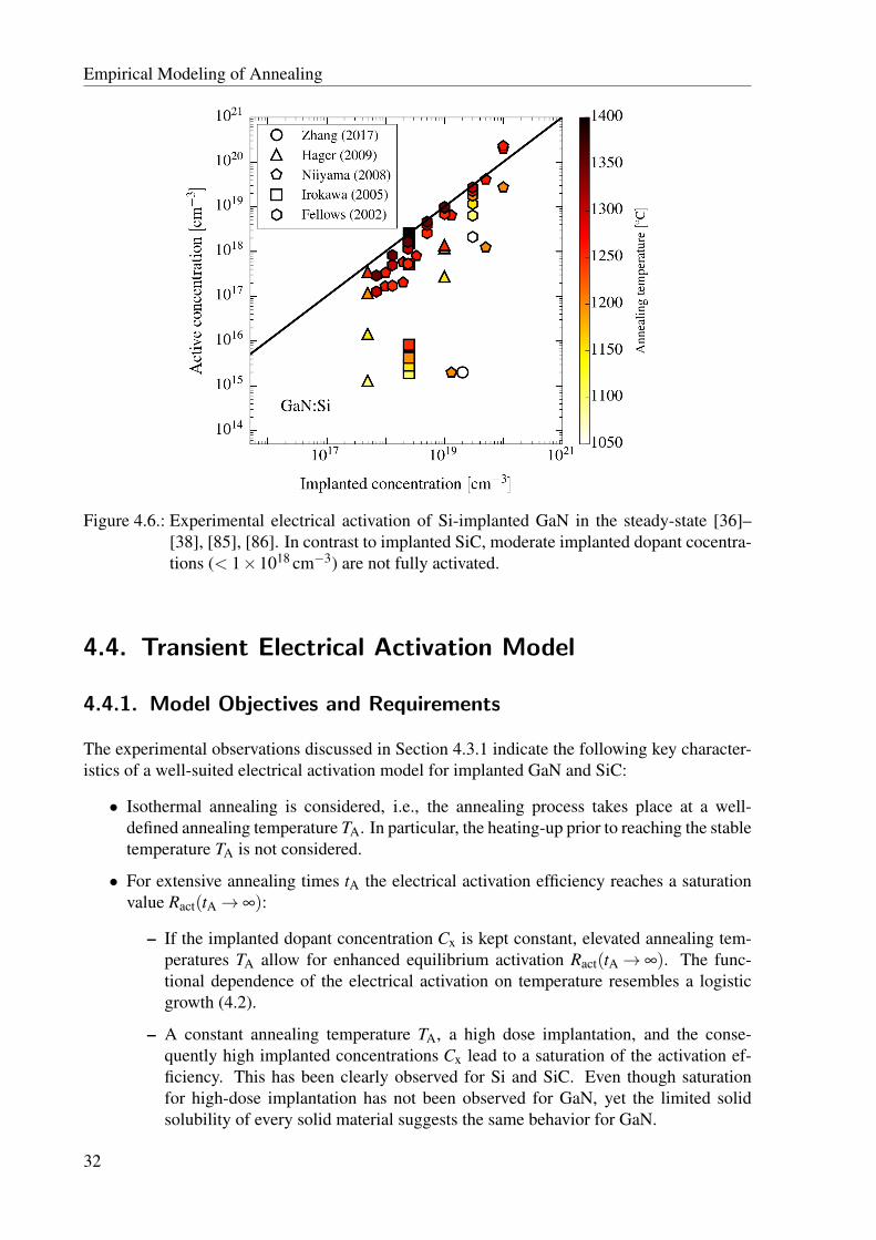
Empirical Modeling of Annealing
Figure 4.6.: Experimental electrical activation of Si-implanted GaN in the steady-state [36]–[38], [85], [86]. In contrast to implanted SiC, moderate implanted dopant cocentra-tions (< 1×1018 cm−3) are not fully activated.
4.4. Transient Electrical Activation Model
4.4.1. Model Objectives and Requirements
The experimental observations discussed in Section 4.3.1 indicate the following key character-istics of a well-suited electrical activation model for implanted GaN and SiC:
• Isothermal annealing is considered, i.e., the annealing process takes place at a well-defined annealing temperature TA. In particular, the heating-up prior to reaching the stabletemperature TA is not considered.
• For extensive annealing times tA the electrical activation efficiency reaches a saturationvalue Ract(tA→ ∞):
– If the implanted dopant concentration Cx is kept constant, elevated annealing tem-peratures TA allow for enhanced equilibrium activation Ract(tA→ ∞). The func-tional dependence of the electrical activation on temperature resembles a logisticgrowth (4.2).
– A constant annealing temperature TA, a high dose implantation, and the conse-quently high implanted concentrations Cx lead to a saturation of the activation ef-ficiency. This has been clearly observed for Si and SiC. Even though saturationfor high-dose implantation has not been observed for GaN, yet the limited solidsolubility of every solid material suggests the same behavior for GaN.
32
Empirical Modeling of Annealing
– Dopants in SiC can be fully activated (Ract = 1) for low dose implantation (providedsufficiently long tA and elevated TA). For silicon implantation into GaN, incompleteactivation for low implanted doses Cx were reported.
– The saturated active dopant concentration Ca,f is related to the solid solubility of theimplants in the host material.
• The annealing kinetics are accelerated by high annealing temperatures tA. If the annealingtemperature is too low, even a very long annealing time tA does not lead to full activation.
• The initial activation efficiency Ract(tA = 0) serves as the initial condition for the modelthat aims to describe an isothermal process. It does not depend to the specific heating-upbehavior of the annealing equipment.
In the following section an empirical model that is capable to describe all these features ispresented. First, the model is formulated in a way that is directly applicable to SiC. Second(Section 4.5), a model modification that accounts for the peculiarities of Si-implanted GaN ispresented.
4.4.2. Activation Model for SiC
The activation process is described as a chemical reaction. The reaction rate is assumed tobe directly proportional to the inactive dopant concentration. However, the maximum activedopant concentration is limited. The upper bound corresponds to the (electrically) active dopantconcentration in thermal equilibrium Ca,f and is related to the implanted concentration Cx usingthe expression
Ca,f(TA,Cx) =Cx
1+ CxCss(TA)
. (4.3)
The saturation behavior is incorporated by introducing the parameter Css(TA), which is a func-tion of the annealing temperature TA. Css(TA) is linked to the solid solubility of a dopant mate-rial in the host crystal. High solid solubility refers to high values of Css(TA).
The annealing kinetics is modeled as a simple first order process with the upper limit Ca,f (seeFigure 4.7). The reaction rate R is given by
R =dCa
dtA= kr(TA)
(Ca,f(TA,Cx)−Ca
), (4.4)
where kr(TA) is the temperature dependent reaction rate coefficient. kr(TA) is assumed to followan Arrhenius law, consistent with common practice in chemical kinetics [87]. Likewise, Css(TA)is expected to follow an Arrhenius equation,
kr(TA) = Akrexp
(− Ekr
a
kBTA
), Css(TA) = ACssexp
(− ECss
a
kBTA
). (4.5)
33

Empirical Modeling of Annealing
In both cases the activation energy Ea is a positive quantity. The analytical solution of (4.4) is
Ca(tA,TA,Cx) = Aexp [−kr(TA) tA]+Ca,f(TA,Cx), (4.6)
with A < 0. Incorporating the initial condition Ca,0 =Ca(tA = 0) yields
Ca(tA,TA,Cx) =[Ca,0−Ca,f(TA,Cx)
]exp [−kr(TA) tA]+Ca,f(TA,Cx). (4.7)
Ca,0 is not related to the physical situation immediately after implantation. Thus, the initialcondition can not be derived from measurements. Keeping in mind that the proposed model isonly valid for tA somewhere in the order of a few seconds, the initial condition Ca(ti) can beshifted to a specific tA = ti 6= 0. The analytical solution is then
Ca(tA,TA,Cx) =[Ca(ti)−Ca,f(TA,Cx)
]exp [kr(TA)(ti− tA)]+Ca,f(TA,Cx). (4.8)
The important difference compared to (4.7) is the fact that Ca(ti) can be directly determined fromannealing measurements. With Ca(tA,TA,Cx) established, the electrical activation efficiency isgiven by
Ract(tA,TA,Cx) =Ca(tA,TA,Cx)
Cx. (4.9)
Figure 4.7.: Active dopant concentration in thermal equilibrium Ca,f(TA,Cx), as modeld by(4.3). For low implanted concentrations, i.e., CxCss(TA), the implanted dopantscan be fully activated. Saturation occurs for high implantation concentration, i.e.,CxCss(TA). The black line represents full activation.
34

Empirical Modeling of Annealing
(4.7) is capable to describe the isothermal annealing process according to the main objectivesgiven in Section 4.4.1. Two phase diagrams, as given in Figure 4.8, visualize the model pre-dictions. In accordance with the objectives a combination of elevated annealing temperaturesand sufficiently long annealing times leads to full activation, i.e., Ract > 0.95. On the one hand,full activation cannot be achieved even after hours if the annealing temperature is too low (e.g.1500 C in Figure 4.7). On the other hand, the annealing process can be considerably shortened(tA < 1min) if the equipment allows to raise the annealing temperature above 1800 C. Theconcentration dependence is appropriately modeled as well. Low dopant concentrations can befully activated even at low annealing temperature. In contrast, implanted concentrations close tothe solid solubility limit (see also Section 2.2.3) cannot be fully activated even when employingextreme annealing temperatures (TA > 2200C).
For a specific annealing time tA = const., the temperature dependence implied by the model isillustrated in Figure 4.9. The model can qualitatively reproduce a logistic-function type growththat is evident from measurements (Figure 4.1b). From a mathematical point of view, this isa direct consequence of the assumption that Css(TA) follows an Arrhenius law. Therefore, theArrhenius assumption is confirmed to be in accordance with the experimental observations.
The steady-state activation Ract(tA→ ∞) is determined by the active dopant concentration inthermal equilibrium Ca,f(TA,Cx), which depends on the ratio Cx/Css(TA). The definition of (4.3)implies that a doping level equal to Css(TA) is only 50% activated. Therefore, the experimentaldata indicates that Ca,f is necessarily smaller than the chemical solid solubility1.
(a) (b)
Figure 4.8.: Phase diagrams illustrating the impact of the annealing process parameters on theelectrical activation of Al-implanted 4H-SiC (Cx = 1×1018 cm-3). (a) Electricalactivation efficiency as a function of annealing time and (b) steady-state activationefficiency as a function of annealing temperature.
1It is important to differentiate the physical/chemical quantity ’solid solubility’, the annealing temperature de-pendent function Css(TA), and the active dopant concentration in thermal equilibrium Ca,f(TA,Cx). The defi-nition (4.3) shows that Ca,f(TA,Cx) depends not only on the annealing temperature, but also on the implanteddopant concentration. The maximum electrically active dopant concentration is thus not only determined bythe annealing temperature. This is due to the observation that in an environment of high chemical dopant con-centration, dopant atoms can form bonds to other dopant atoms. In this way, clusters and defect-configurationsinvolving bulk crystal vacancies and interstitials can be formed.
35

Empirical Modeling of Annealing
Figure 4.9.: Calculated active dopant concentration as a function of annealing tem-perature for specific annealing times and implanted dopant concentrations,(a) Cx = 1×1020 cm−3 and (b) Cx = 1×1019 cm−3. The empirical activationmodel (4.4) reproduces the abrupt raise of activation efficiency observed in ex-periments as shown in Figure 4.1b.
Even though it is possible to use the time-shifted solution (4.7) to determine the kinetic modelparameter kr(TA) from the measurement data, the choice of initial activated dopant concentra-tion Ca,0 in (4.6) turns out to have only minor impact. As long as the initial dopant concentrationis considerably smaller than the steady-state value (Ca,0Ca,f) the reaction coefficient kr(TA) isnot significantly influenced. This assumption is justified for the wide-bandgap semiconductorsSiC and GaN, because an active dopant concentration prior to the annealing step is not measur-able. Thus, (4.6) can also be employed if Ca,0 is set to a relatively small value (compared toCa,f(TA,Cx)). A straightforward relation can be used:
Ca,0 = F Ca,f(TA,Cx) (4.10)
where F is as an empirical parameter that is typically ≈ 10−3.
The model presented above accurately reproduces the activation characteristics observed inimplanted SiC. In order to describe implanted GaN’s divergent behavior, a model extension isproposed in the following section.
36

Empirical Modeling of Annealing
4.5. Activation Model Extension for GaN
For low doping concentrations CxCss(TA) the definition (4.3) assumes full activation Ca =Cxin the steady-state case (tA→ ∞). The divergent behavior for Si-implanted GaN, which is char-acterized by a reduced activation efficiency, cannot be described. However, the addition of thefactor (Cx/Css(TA))
α with the empirical parameter α > 0 allows to reproduce this behavior
C′a,f(TA) =
Cx
(Cx
Css(TA)
)α
1+Cx
(Cx
Css(TA)
)α
Css(TA)
. (4.11)
Figure 4.10 illustrates that the modified model reproduces the original transient activation modelfor α = 0. Increasing the empirical factor α gradually tilts C
′a,f away from full activation
C′a,f =Cx. The maximum active concentration is still governed by the solid solubility related
parameter Css.
The reason for the low activation level prevalent for small implanted concentration is contro-versially discussed (see Section 2.2.4) in the literature. Assuming the very likely case thatunintentionally introduced compensating dopants play an important role, α is related to thecompensating species concentration. The higher the concentration, the higher is α . For thiswork, the experimental data (Figure 4.6) suggests that α obeys an Arrhenius law, which is fur-ther discussed in Section 4.7.2. However, governed by an Arrhenius law α attains very highvalues for annealing temperatures below the typically employed temperatures (< 1200C). Asa consequence, (4.11) degenerates to a function similar to a step function, which is unphysical2.Limiting the maximum value of α avoids this problem. A reasonable upper limit for α , whichis consistent with the available data is 2. Thus, the valid range is 0≤ α < 2.
For empirical models the calibration with respect to the experimental data is crucial. The nextsection examines the numerical techniques that are employed to estimate the model parame-ters.
4.6. Model Parameter Estimation - Nonlinear Regression
The proposed transient annealing model features three parameters for electrically active dopants:the reaction rate kr, the solid solubility related parameter Css, and the initial active concentra-tion Ca,0 (for the modified model there is also the empirical exponent α). If (4.10) is applied thenumber of independent parameters is reduced by one. The remaining two (three) parametersare estimated from the experimental data employing regression analysis.
The model parameter estimation procedure consists of two steps. In the first step the annealingdata for constant annealing temperature TA = T 0
A is considered. For constant annealing tem-perature the active concentration depends only on the annealing time and the implanted dopant
2At low annealing temperatures and Cx > Css(TA) the modified model predicts the active concentration tobe equal to the solid solubility coefficient Css(TA). This is a consequence of α assuming high val-ues, i.e., limα→∞ C
′a,f(TA) =Css(TA). For Cx <Css(TA) extremely low activation efficiencies are achieved,
limα→∞ C′a,f(TA) = 0.
37

Empirical Modeling of Annealing
Figure 4.10.: The empirical modification of (4.3) given in (4.11) allows to describe the charac-teristical low activation level for small implanted dopant concentrations found inGaN.
concentration Ca(tA,Cx)|TA=T 0A
. kr(T 0A) and Css(T 0
A) are estimated by solving a least squaresproblem in order to achieve the best fit of (4.7) to the experimental data. This procedure isrepeated for all available annealing temperatures T i
A. The results are further processed in thesecond step, where the prefactors Akr,Css and activation energies Ekr,Css
a are determined by solv-ing a second least squares problem for (4.5).
The least squares problem is a commonly occurring problem in science and engineering and ismathematically stated in Definition 4.6.1 [88].
Definition 4.6.1 (Least Squares Problem)Find a local minimizer a∗ ∈ Rn for
F(a) =m−1
∑j=0
f 2j (a),
with given functions f j : Rn→ R, j ∈ 0, . . . m−1 and m≥ n.
The function F : Rn→ R is called cost function or score function. The curve fit problem for agiven data set can be solved by appropriately defining the cost function, see Definition 4.6.2.
38

Empirical Modeling of Annealing
Definition 4.6.2 Cost Function for the Regression AnalysisLet D = (x0,y0), (x1,y1), . . . , (xm−1,ym−1) ⊆R2 be a set of m data points and g(x;a) ananalytical one dimensional function g : R→ R with parameters a ∈ Rn. The cost functionfor the non-linear regression analysis is
F(a) =m−1
∑i=0
[yi−g(xi;a)]2 .
In the discussed parameter estimation procedure the function g(x;a) assumes the form of (4.7)in the first step and of (4.5) in the second step, respectively. Both functions are nonlinearfunctions of the parameters a = [kr,Css,(α)]ᵀ. Consequently, iterative numeric schemes haveto be employed to solve the least squares problem. One example is the Levenburg-Marquardtgradient method [88].
The parameter estimation procedure has been performed for all the dopant-host material com-binations given in Section 4.3, resulting in a calibrated electrical activation model, as demon-strated in the following sections.
4.7. Calibration of Activation Models
In order to confirm that the proposed model can accurately reproduce the experimental data,Arrhenius plots of the reaction rate coefficient kr(TA) and the solid solubility parameter Css(TA)are examined. First, implanted 4H-SiC, for which the plethora of experimental data for differentdopants is available, is considered. Second, the modified activation model is calibrated for Si-implanted GaN.
4.7.1. Implanted 4H-SiC
Figure 4.11a shows the calibrated model for Al implantation versus the experimental data fromNipoti et al. [62] for different annealing temperatures. Similar curve fits for all available anneal-ing temperatures result in the kr(TA) and Css(TA) plots depicted in Figure 4.11b. The annealingtemperature dependence of these parameters can be accurately described by an Arrhenius law.
The lack of comprehensive activation kinetics studies for implanted B only allows to calibratethe activation model for the steady-state activation. Thus, only the solid solubility parame-ter Css(TA) is determined (as shown in Figure 4.12a). Compared to implanted Al the signifi-cantly limited data causes higher uncertainty about the obtained parameter values. Nevertheless,Css(TA) follows an Arrhenius law (Figure 4.12b).
The steady-state activation data for implanted N indicates that the solid solubility parametersobeys an Arrhenius law (Figure 4.13a and Figure 4.13b). The activation kinetics in particularhave been investigated by Blanque et al. [76] (see Figure 4.5). Their measurements allow to
39
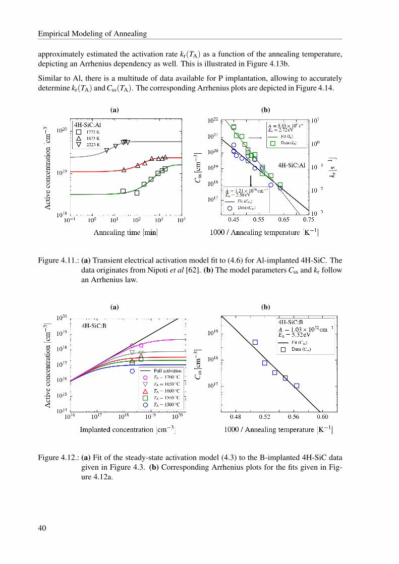
Empirical Modeling of Annealing
approximately estimated the activation rate kr(TA) as a function of the annealing temperature,depicting an Arrhenius dependency as well. This is illustrated in Figure 4.13b.
Similar to Al, there is a multitude of data available for P implantation, allowing to accuratelydetermine kr(TA) and Css(TA). The corresponding Arrhenius plots are depicted in Figure 4.14.
(a) (b)
Figure 4.11.: (a) Transient electrical activation model fit to (4.6) for Al-implanted 4H-SiC. Thedata originates from Nipoti et al [62]. (b) The model parameters Css and kr followan Arrhenius law.
(a) (b)
Figure 4.12.: (a) Fit of the steady-state activation model (4.3) to the B-implanted 4H-SiC datagiven in Figure 4.3. (b) Corresponding Arrhenius plots for the fits given in Fig-ure 4.12a.
40

Empirical Modeling of Annealing
(a) (b)
Figure 4.13.: (a) Fit of the steady-state activation model (4.3) to the N-implanted 4H-SiC datagiven in Figure 4.5. (b) Arrhenius plot of the model parameters Css and kr, whichare determined from the fits given in Figure 4.13a.
Figure 4.14.: Arrhenius plots of the model parameters Css and kr for P-implanted 4H-SiC.
4.7.2. Implanted GaN
The modified activation model is employed for Si implanted GaN. Figure 4.15 demonstratesthat the reduced activation efficiency for low concentrations is well reproduced. The corre-sponding solid solubility parameter Css(TA) follows an Arrhenius law in total analogy to itsbehavior for implanted SiC. The empirical exponent α is found to obey an Arrhenius law withnegative activation energy. However, as pointed out in Section 4.5, α is only valid within theannealing temperature range that has been experimentally investigated. α can be assumed tohave an upper limit, which is of importance for low temperatures. A further assumption is thatthe employed capping technology (e.g., AlN or SiO2 caps) discussed in Section 2.2.4 does not
41

Empirical Modeling of Annealing
significantly influence the activation efficiency and, thus, the data from different experimentscan collectively be considered in order to calibrate the activation model.
In conclusion, the proposed activation models have the capability to describe the impact of theannealing process parameters on the transient and equilibrium electrical activation of implanteddopants. The model parameters have been calibrated with respect to data from SiC and GaNannealing experiments. The activation models allow to accurately reproduce the experimentalobservations and can be employed within comprehensive semiconductor process simulations,which are discussed in the next chapter.
[!h]
Figure 4.15.: Electrically active concentration Ca,f for Si-implanted GaN as function of im-planted concentration Cx for various annealing temperatures TA. The solid linesshow the fit of the modified activation model (4.11) (solid lines) to the experimen-tal data [36]–[38], [85] (open symbols). The obtained model parameters Css andα are fitted with the Arrhenius equation, as shown in the inset figure.
42

5. Process and Device Simulations
The post-implantation annealing modeling discussed in the previous chapters plays a decisiverole in semiconductor process simulations. Process simulations are an integral part of TCAD,which allows to harness the complexity of design and fabrication of semiconductor devices andsystems. The challenging fabrication processes of SiC and GaN lead to significantly higherproduction costs compared to the Si technology. The predictive power of TCAD facilitatesprocess integration and optimization and allows to examine the impact of process parameterson the device characteristics.
In this chapter the role of TCAD for wide-bandgap semiconductor device fabrication is dis-cussed. The activation models presented in this work are integrated into comprehensive coupledprocess and device simulations of state-of-the-art power devices, the 4H-SiC DMOSFET andthe GaN JBS rectifier. The simulation results provide valuable information about the influenceof annealing parameters on device operation, which is essential for process optimization.
5.1. Technology Computer-Aided Design
In semiconductor fabrication, computer-aided modeling and simulations aim at supporting tech-nology development and optimization and thus reducing development times and costs. ClassicalTCAD comprises front end process, device and interconnect modeling. However, in a broadercontext, the interplay between classical TCAD to equipment (e.g. lithography) and integratedcircuit-scale (e.g., circuit elements and packaging) modeling is crucial for microsystem design.Therefore, the term extended TCAD has been established [89].
TCAD is highly valuable, because TCAD tools provide better insights in process and devicecharacteristics. Additionally, TCAD allows to examine the optimum doping well width, peakdoping concentrations, epitaxial layer, or oxide thicknesses in cost-effective way. After thecalibration of the employed model to a set of experimental data, the model has predictive power,which allows to improve existing technology and investigate novel device structures [90]. Theempirical activation model that is proposed in Chapter 4 part of process modeling on the featurescale. Hence, the annealing equipment is not modeled, but its impact on the sample is (bymeans of annealing temperature and time). Process simulations are especially useful when theyare combined with device simulations, because the impact of process parameters on the devicecharacteristics can be studied.
The impact of fabrication processes and their parameters on the device characteristics is inparticular important for GaN and SiC, where the process steps have not yet been fully optimized.In the following sections the techniques that are employed to model the fabrication processesand operations of wide-bandgap power devices are discussed.
43

Process and Device Simulations
5.1.1. Process Simulations
Semiconductor process simulations deal with predicting the geometrical and physical impactof all process steps that are needed to fabricate semiconductor devices. During a process sim-ulation both geometrical and physical problems have to be formulated and solved. The pat-terning of semiconductor structures is based on additive (e.g., thin film growth) and subtractive(e.g., etching) process, which are ultimately controlled by a sequence of lithography masks.For lithography the desired device geometry has to be specified by means of two-dimensionalmasks. Complex device structures (such as solid-state memories) require dozens of patterningsteps and geometry-based simulations provide the tools to optimize them.
However, in order to account for the highly important non-ideal effects such as bird’s peak,under-etching, or introduction of film stress, physical models are valuable for process simu-lations. The thickness of thermally oxidized or epitaxially grown films can be described as afunction of time and further process parameters. The mechanical stress, which is introducedby lattice mismatch, impurity atoms, or electric fields is subject to continuum mechanisms.The multitude of processes occurring during ion irradiation (involving redeposition, surfacediffusion and impurity cluster formation), require a combined geometrical and physical ap-proach [91].
Continuous physical models typically assume the form of (3.15), where the dopant and defectdiffusion is described with continuous distributions of physical quantities. However, the contin-uum approach has its limitations, which can be overcome by atomistic methods in some cases.One important example are probabilistic Monte Carlo ion implantation simulations (i.e., binarycollision simulations), where the trajectory of individual ions as they enter the semiconductor iscalculated. In order to accurately account for the lattice damage induced by the collision of ionswith host atoms, the interatomic potentials and nuclear and electronic stopping mechanismshave to be modeled [92].
Physical models are often time-consuming (e.g., Monte Carlo ion implantation) or require infor-mation about micro-physical processes, which is often not available. As discussed in Chapter 3,the understanding of the micro-physics associated with annealing after an implantation stepis not yet sufficient for most impurity-host material combinations. In such a case, empiricalmodels come into play (as discussed in Chapter 4).
The examples given above corroborate that semiconductor process simulations solve multi-physics and geometrical problems. Several process simulation tools are available, however,in this work, Silvaco’s Victory Process [91] simulator, which is capable of two- and three-dimensional simulations, is used. Process simulations are initiated by providing a list of state-ments that describe the processing steps and geometrical information via implantation masks.Victory Process implements various highly specialized numerical techniques, such as multi-material surface evolution and adaptive grid resolutions. These techniques are crucial for thedemanding environment of multi-physics process simulation on a mutable geometry. The re-sulting device structure can be directly used to conduct device simulations, which are discussedin the next section.
44

Process and Device Simulations
5.1.2. Device Simulations
A semiconductor device simulation aims to describe the electronic transport enforced by ex-ternally applied voltages and currents. With accurate device simulations the most importantdevice parameters, i.e., the figure of merits, can be optimized. Modern semiconductor devicesrely on sophisticated doping profiles and complex current paths that cannot be easily modeledwith simple one-dimensional compact-models.
A set of semi-classical differential equations, referred to as Drift-Diffusion equations has provensuccessful to calculate (charge) carrier and current density distributions in large-area Si devices.Even though these equations are insufficient for nano-scale devices [93], typical power devicestructures with dimensions in the µm regime can be accurately treated with them. The currentdensities in the semiconductor are determined via the continuity equations
∇ ·Jn−q∂n∂ t
= qR, (5.1)
∇ ·Jp +q∂ p∂ t
=−qR, (5.2)
which result from conservation of electrical charge. A spatial gradient in the electron currentdensity Jn (hole current density Jp) induces temporal change of the electron concentration n(hole concentration p). Additionally, charge carriers can be generated (e.g., optically or bycharge injection), which is modeled with the generation/recombination rate R. q is the elemen-tary charge. A distribution of carrier interacts with each other by Coulombic forces. Therefore,the Poisson equation
∇2ϕ =
qε(n− p+N−A −N+
D ) (5.3)
is employed with the electric potential ϕ , the semiconductor’s permittivity tensor ε , and the con-centration of electrically active and ionized acceptors N−A and donors N+
D . The Drift-Diffusionequations [94]
Jn =−qµn(∇ϕ−VT∇n), (5.4)Jp =−qµp(∇ϕ +VT∇n) (5.5)
state that the current densities are evoked by gradients in ϕ (drift component) and in the carrierdensity (diffusion component). VT is the thermal voltage VT = (kBT )/q. The carrier’s responseto an applied electric field is described by the mobility µn,p. In the case of the hexagonal semi-conductor 4H-SiC, the mobility is anisotropic. The mobilities for current along the hexagonalc-axis (‖) and perpendicular directions (⊥) are different with the typical values [95]
µn,⊥ = µn, µp,⊥ = µp, (5.6)µn,‖ = 1.2 µn, µp,‖ = µp. (5.7)
In order to account for the special material properties of wide-bandgap semiconductors, theincomplete ionization and the mobility have to be accurately modeled. The former is linked to aphenomenon, which is referred to as freeze-out. Even if a dopant is electrically active (after anannealing step), electrons can be strongly bound to it, prohibiting the electrons to contribute tothe conduction current (and consequently ionizing the dopant). Due to large ionization energies,partial freeze-out is observed in SiC even at room temperature. The relation between ionized
45

Process and Device Simulations
dopant concentrations N+,−D,A and electrically active dopant concentrations ND,A can be modeled
using the expression [94], [96]
N+,−D,A =
ND,A
1+gD,Aν
NC,Vexp(
EBkBT
) , ν = n, p, (5.8)
which can be derived from statistical mechanics [97]. Dopant ionization is a thermally promotedprocess with an activation energy EB = EC−ED in the donor case and EB = EA−EV in theacceptor case. EC and EV refer to the conductance band edge and valence band edge energy,respectively, and ED and EA characterize the dopant’s energy level1. Additionally, the degree ofionization depends on the degeneracy factors gD,A
2. NC,V are the effective densities of states forthe conduction and valence band, respectively. However, in 4H-SiC the dopants can reside onhexagonal and cubic lattice sites, which is accounted for by the two-level incomplete ionizationmodel, which introduces one expression in the spirit of (5.8) for each type of lattice sites [98].
Mobility modeling is highly important for every semiconductor device, but in particular forMOSFETs. In a MOSFET, the carriers transversing the channel are subjected to high electricalfields and surface scattering, which reduces the mobility values compared to the bulk mobility.A comprehensive mobility model, which has been specifically proposed for 4H-SiC, is theUhnevionak model [17]. In the Uhnevionak model, the mobility is constructed as the sum ofindividual influences according to Matthiessen’s rule
1µn,p
=1
µIMP+
1µBP
+1
µC+
1µSR
+1
µSP. (5.9)
The contributions from Coulomb scattering at ionized impurities (IMP), bulk-phonon scattering(BP), scattering at interface charges (C), surface roughness (SR), and surface phonon scattering(SP) allow to accurately model the electron mobility in the DMOSFET channel. For otherdevice structures, such as the JBS rectifier, surface and interface effects can be neglected.
The generation rate R is another quantity that is strongly material dependent. It is importantto correctly account for generation-recombination phenomena, because they critically affectleakage currents and device breakdowns [23]. Indirect generation-recombination, which in-volves electron and hole capture and emission processes via trap centers, is commonly modeledwith the Shockley-Read-Hall (SRH) model. Auger-processes, which involve three particlesthat interact due to their high thermal energy, can also be described with additional generationterms.
Silvaco’s Victory Device [96] is a commercially available general purpose device simulator,which, among others, solves the semiconductor equations discussed above. The simulationdomain is subdivided into discrete elements (e.g. tetrahedrons in three dimensions), which allowto discretize the coupled differential equations. The resulting nonlinear system of algebraicequations is solved with the help of Newton’s method. Victory Device allows to simulate thedevice structures originating from Victory Process, which thereby offering to model the entireworkflow, from fabrication to the evaluation of the electrical characteristics. As far as mobilitymodeling is concerned, various models are available for both wide-bandgap semiconductors
1(5.8) is commonly given in the form N+D = ND/(1+gD exp [(EF−ED)/(kBT )]) with the Fermi level EF and
the donor level ED. Within the framework of Maxwell-Boltzmann statistics both formulations are equivalent,because n = NC exp [(EF−EC)/(kBT )]. For ionization of acceptors similar equations hold.
2The degeneracy factors characterize the number of ways an electron can assume a localized state [97].
46

Process and Device Simulations
examined in this work. The model parameter can be flexibly chosen, allowing to accuratelysimulate power DMOSFETs and JBS rectifiers, as discussed in the next sections.
5.2. SiC Power DMOSFET
A DMOSFET is a vertical current device, which was first realized in Si technology. SiC-basedDMOSFETs have been presented in the early 2000s and have been optimized since then [99]–[101]. In the following, the commonly employed DMOSFET structure with dimensions anddoping profiles reported by Saha et al. [102] is considered. The fabrication process is simulatedand the output characteristics of the resulting DMOSFET are calculated, allowing to study theimpact of thermal annealing on the device properties.
5.2.1. SiC DMOSFET Structure
Figure 5.1 shows the schematic cross section of a 4H-SiC (n-type) DMOSFFET. A n-type4H-SiC epilayer is grown on a highly n-doped (n+) substrate. In order to form the channel,a p-type well (referred to as bulk) is required. In Si technology, the p-type well is realizedusing doping by diffusion. However, the low diffusion coefficients of dopants in SiC requireto employ the ion implantation technique. The p-type well is referred to as the DMOSFET’s’bulk’. Similar to a lateral MOSFET structure highly n-doped source regions are formed. Thedrain region is located at the wafer backside, enforcing a vertical current flow. The gate contactallows to control the surface carrier concentration in the channel via the gate oxide, which isalso depicted in Figure 5.1. Strikingly, the electron current is guided along the wafer surfacebefore it transitions into the vertical direction. This ensures excellent electrostatic control andenhances the drain current by reducing the channel length.
The highly doped p-type and the n-type region are shortened to turn off the parasitic bipolarjunction transistor, which is formed by the p+-region, the n+-well, and p-type well. The p-welland the drain region form a pn-diode (referred to as bulk-drain diode), which is required toblock the transverse current for positive drain-source voltages VDS. Its breakdown voltage canbe precisely controlled by the doping concentration. For negative VDS the bulk-drain diode doesnot block the current and the DMOSFET operates as pn-rectifier, which can be beneficiallyutilized in power electronics [103].
The DMOSFETs device structure allows to realize power switches capable of controlling drainvoltages in the kV regime with negligible leakage currents. The parallel circuit structure enablesa favorable high input capacitance enabling fast switching speed (≈ 100ns) and drain currentsin the kA regime with on-state resistances Ron that are at least two orders of magnitude lowerthan for Si devices [99].
The main design goal is to minimize Ron and the chip area while maintaining a high blockingvoltage. In order to achieve that, a heavily n-doped region, which is referred to as junction fieldeffect transistor (JFET) region, has been proposed [2]. In particular, the JFET region allows toreduce the distance between two adjacent source regions and thus the chip area. However, thisis at the cost of an enhanced on-resistance. A self-aligned sub-micron channel further reducesthe channel length and current crowding is avoided by homogenizing the trapezoidal electron
47

Process and Device Simulations
Drain
n+-SiC Substrate
n-SiC Epilayer
n-SiC Current Spreading Layer (CSL)
n-JFETp-SiC Well
p+-SiC n+-SiC WellOxide
GateSource
Figure 5.1.: Schematic cross-section of the examined 4H-SiC DMOSFET. The vertical line cor-responds to the cut that is used for the doping depth profiles in Figure 5.3. Quanti-ties along the horizontal line are discussed in Figure 5.6a.
flow from the JFET region into drift region with the help of an epitaxial n-type current spreadinglayer (CSL), which is also shown in Figure 5.1 [102].
5.2.2. SiC DMOSFET Process Simulations
Starting with a highly doped n-type 4H-SiC substrate the following process steps are simulatedwith Victory Process:
• Epitaxial growth of a lightly n-doped 6 µm epitaxial layer (ND = 1×1016 cm−3).
• Epitaxial growth of a 0.9µm n-doped layer (ND = 1×1017 cm−3). This layer forms theCSL layer and the JFET region in the final device.
• Selective deposition of the implantation mask (SiO2).
• Ion implantation of aluminum (p-type dopant) and P (n-type dopant) to form the p-well,highly doped n-well, and the highly p-doped region below the source contact. The im-plantation energies are chosen to produce a p-well with a depth of 0.6µm.
• Annealing step employing the empirical activation model (discussed in Chapter 4). Thesurface is capped with SiO2.
• Thermal oxidation to form the gate oxide with a thickness of 50 nm.
• Metal deposition to form the contacts (source, gate, and drain).
These process steps result in the DMOSFET structure shown in Figure 5.2, where the activeregion near the surface is depicted in detail (Figure 5.2). Only one half-cell of the complete de-vice is shown. This is sufficient for device simulations, because the total cell can be constructedby mirroring the half-cell along the vertical axis. The geometrical dimensions are chosen toreproduce the device presented by Saha et al [102].
48

Process and Device Simulations
Figure 5.2.: Victory Process cross section of the investigated 4H-SiC DMOSFET. The colorsillustrate the (electrically active) net doping concentration NNet = ND−NA. Thearrows show that the conduction current flows vertically from the drain to the chan-nel and transitions to lateral flows along the surface to leading to the source contact.
(a) (b)
Figure 5.3.: DMOSFET doping depth profiles along the line given in Figure 5.2. (a) The maxi-mum active P concentration is limited by the annealing temperature TA = 1600C.Even extending the annealing time from tA = 5min to 8min does not increase theactivation efficiency. For implanted Al this is not the case, because the total im-planted concentration is two orders of magnitude lower. (b) For constant annealingtime the strong impact of annealing temperature on the maximum activation effi-ciency is observed for the highly P-doped regions. The low Al-implanted concen-tration can be nearly fully activated even at reduced temperatures.
49

Process and Device Simulations
The n+ source region is modeled to exhibit a peak donor concentration of 1×1020 cm−3 in ac-cordance with Saha et al. The Al implantation doses forming the p-well are chosen to produce afully functional DMOSFET device under the assumption of fully activated implanted dopants.However, the electrical activation ratio depends on annealing time tA, annealing temperature TA,and implanted concentration Cx as stated by the empirical activation model (see Section 4.4).Figure 5.3 illustrates the depth doping profiles (vertical cut through n+-well and p-well) anddemonstrates the predictions of the empirical activation model for several annealing tempera-tures and annealing times. Saha et al. employed TA = 1600C and tA = 5min, also shown inFigure 5.3.
For a constant annealing temperature a transient saturation can be observed. While the activealuminum concentration is increased threefold by extending the annealing time from 1 minto 5 min, a 8 min annealing steps only results in an further improvement of 30%. The highconcentration of implanted P causes a drastically reduced activation efficiency compared to theimplanted aluminum profile. Furthermore, the activation kinetics of implanted P is faster withthe maximum activation already reached after 5 min. The maximum activation efficiency ofonly approximately 2% is noticeably small, indicating that higher annealing temperatures areneeded to activate P doping profiles with concentrations in the order of 1020 cm−3. In contrast,the annealing temperature TA = 1600C allows to achieve an aluminum activation of ≈ 85%after 8min.
Figure 5.3b illustrates the impact of TA for a constant tA = 5min on the doping profile. In partic-ular, elevated annealing temperatures (TA = 1700C) allow to increase the aluminum activationratio from 73% to 93%. The achievable P activation ratio is limited by solid solubility and thusonly amounts to approximately 3% of the implanted peak concentration.
5.2.3. SiC DMOSFET Device Simulations
Silvaco’s Victory Device simulator [96] allows to simulate the device characteristics for devicestructures obtained by Silvaco’s Victory Process simulator. The considered 4H-SiC DMOSFETis a large-area device, which enables a semi-classical modeling approach.
The models discussed in Section 5.1.2 enable an accurate description of the carrier transport inthe DMOSFET. Additionally, interface states have to be considered. The high density of inter-face states at the SiC-SiO2 interface strongly impacts the MOSFET’s sub-threshold slope, be-cause charge carriers are trapped at the interface, which affects the electrostatics in the channel.Sze [104] analytically determined that the presence of interface states raises the sub-thresholdslope S =VG/(log ID), which is detrimental for device performance (ID and VG refer to the draincurrent and the gate voltage, respectively). The charge trapping process depends on the trap’senergy level and the possible charge states. In 4H-SiC acceptor-like traps, which can assume aneutral or a negatively charged state, are dominating. A simple approach to model the impact ofinterface traps on the device characteristics is to adapt the SRH generation-recombination for-malism, which has been originally established for bulk Si, for the 4H-SiC-SiO2 interface [105].Appendix A provides a comprehensive table that summarizes the employed models and param-eters as they were set in Silvaco Victory Device simulator. The well calibrated device simulatorallows to study the output characteristics (ID vs. VG) of the considered DMOSFET, which ispresented in the following.
50
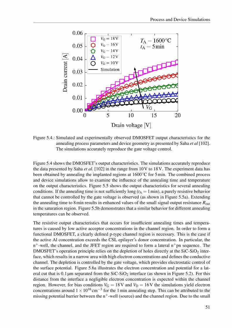
Process and Device Simulations
Figure 5.4.: Simulated and experimentally observed DMOSFET output characteristics for theannealing process parameters and device geometry as presented by Saha et al [102].The simulations accurately reproduce the gate voltage control.
Figure 5.4 shows the DMOSFET’s output characteristics. The simulations accurately reproducethe data presented by Saha et al. [102] in the range from 10V to 18V. The experiment data hasbeen obtained by annealing the implanted regions at 1600C for 5min. The combined processand device simulations allow to examine the influence of the annealing time and temperatureon the output characteristics. Figure 5.5 shows the output characteristics for several annealingconditions. If the annealing time is not sufficiently long (tA = 1min), a purely resistive behaviorthat cannot be controlled by the gate voltage is observed (as shown in Figure 5.5a). Extendingthe annealing time to 8min results in enhanced values of the small signal output resistance Routin the saturation region. Figure 5.5b demonstrates that a similar behavior for different annealingtemperatures can be observed.
The resistive output characteristics that occurs for insufficient annealing times and tempera-tures is caused by low active acceptor concentrations in the channel region. In order to form afunctional DMOSFET, a clearly defined p-type channel region is necessary. This is the case ifthe active Al concentration exceeds the CSL epilayer’s donor concentration. In particular, then+-well, the channel, and the JFET region are required to form a lateral n+pn sequence. TheDMOSFET’s operation principle relies on the depletion of holes directly at the SiC-SiO2 inter-face, which results in a narrow area with high electron concentrations and defines the conductivechannel. The depletion is controlled by the gate voltage, which provides electrostatic control ofthe surface potential. Figure 5.6a illustrates the electron concentration and potential for a lat-eral cut that is 0.1µm separated from the SiC-SiO2 interface (as shown in Figure 5.2). For thisdistance from the interface a negligible electron concentration is expected within the channelregion. However, for bias conditions VG = 18V and VD = 16V the simulations yield electronconcentrations around 1×1016 cm−3 for the 1min annealing step. This can be attributed to themissing potential barrier between the n+-well (source) and the channel region. Due to the small
51

Process and Device Simulations
active Al concentration for this annealing steps, the channel region is flooded with electronsfrom the n+-region. Consequently, electrons assume the role of the majority carrier, whicheffectively results in a continuous n-doped path from source to drain, giving rise to resistiveoutput characteristics.
(a) (b)
Figure 5.5.: DMOSFET output characteristics for different annealing process parameters withconstant (a) TA = 1600C and (b) tA = 5min. If the annealing time or temperatureis insufficient, the purely resistive behavior that cannot be controlled by the gatevoltage is observed (black lines). Extended annealing times and elevated annealingtemperatures results in enhanced output resistances Rout.
The enhanced output resistances for elevated annealing temperatures is caused by a shift of thethreshold voltage. Figure 5.6b illustrates the transfer characteristics (drain current ID vs. gatevoltage VG) for VD = 16V. The characteristics is shifted to higher gate voltage for enhancedannealing temperatures, which corresponds to a threshold voltage shift. This is caused by theenhanced active acceptor concentration in the channel region, which determines the depletioncircumstances. Extended annealing times also lead to a threshold voltage shift.
The combined process and device simulation demonstrate that the annealing process parame-ters have a strong impact on the device characteristics. In a device that is based on multipleimplanted donors, such as the DMOSFET, an accurate description of the electrical activationefficiency is highly beneficial for the device design. Annealing modeling is also crucial for adiode structure, as it is demonstrated in the next section for a GaN JBS rectifier.
52
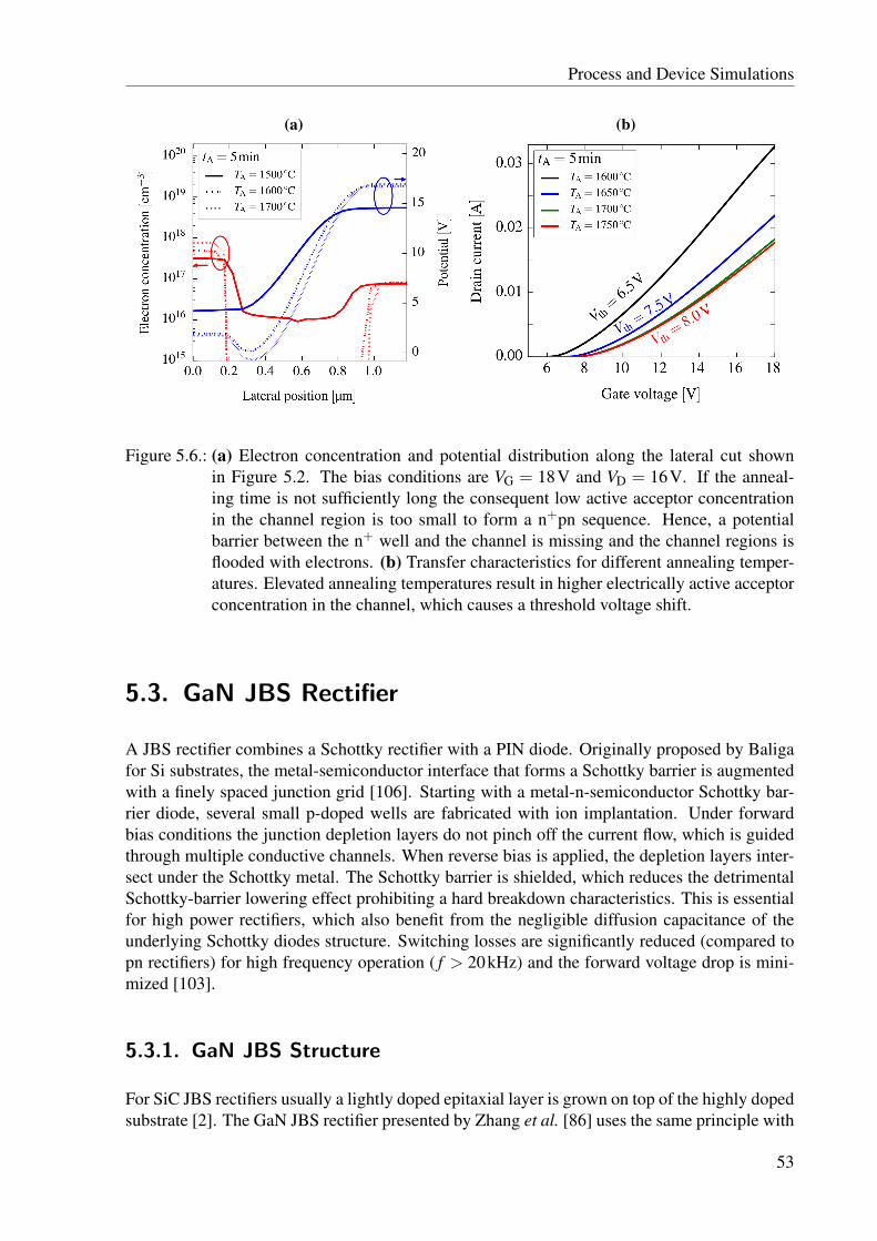
Process and Device Simulations
(a) (b)
Figure 5.6.: (a) Electron concentration and potential distribution along the lateral cut shownin Figure 5.2. The bias conditions are VG = 18V and VD = 16V. If the anneal-ing time is not sufficiently long the consequent low active acceptor concentrationin the channel region is too small to form a n+pn sequence. Hence, a potentialbarrier between the n+ well and the channel is missing and the channel regions isflooded with electrons. (b) Transfer characteristics for different annealing temper-atures. Elevated annealing temperatures result in higher electrically active acceptorconcentration in the channel, which causes a threshold voltage shift.
5.3. GaN JBS Rectifier
A JBS rectifier combines a Schottky rectifier with a PIN diode. Originally proposed by Baligafor Si substrates, the metal-semiconductor interface that forms a Schottky barrier is augmentedwith a finely spaced junction grid [106]. Starting with a metal-n-semiconductor Schottky bar-rier diode, several small p-doped wells are fabricated with ion implantation. Under forwardbias conditions the junction depletion layers do not pinch off the current flow, which is guidedthrough multiple conductive channels. When reverse bias is applied, the depletion layers inter-sect under the Schottky metal. The Schottky barrier is shielded, which reduces the detrimentalSchottky-barrier lowering effect prohibiting a hard breakdown characteristics. This is essentialfor high power rectifiers, which also benefit from the negligible diffusion capacitance of theunderlying Schottky diodes structure. Switching losses are significantly reduced (compared topn rectifiers) for high frequency operation ( f > 20kHz) and the forward voltage drop is mini-mized [103].
5.3.1. GaN JBS Structure
For SiC JBS rectifiers usually a lightly doped epitaxial layer is grown on top of the highly dopedsubstrate [2]. The GaN JBS rectifier presented by Zhang et al. [86] uses the same principle with
53
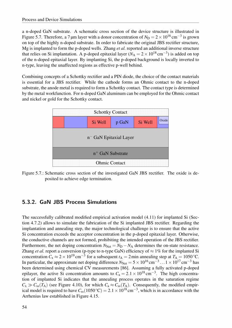
Process and Device Simulations
a n-doped GaN substrate. A schematic cross section of the device structure is illustrated inFigure 5.7. Therefore, a 7 µm layer with a donor concentration of ND = 2×1016 cm−3 is grownon top of the highly n-doped substrate. In order to fabricate the original JBS rectifier structure,Mg is implanted to form the p-doped wells. Zhang et al. reported an additional inverse structurethat relies on Si implantation. A p-doped epitaxial layer (NA = 2×1018 cm−3) is added on topof the n-doped epitaxial layer. By implanting Si, the p-doped background is locally inverted ton-type, leaving the unaffected regions as effective p-well behind.
Combining concepts of a Schottky rectifier and a PIN diode, the choice of the contact materialsis essential for a JBS rectifier. While the cathode forms an Ohmic contact to the n-dopedsubstrate, the anode metal is required to form a Schottky contact. The contact type is determinedby the metal workfunction. For n-doped GaN aluminum can be employed for the Ohmic contactand nickel or gold for the Schottky contact.
Ohmic Contact
n+ GaN Substrate
n− GaN Epitaxial Layer
p GaNSi Well Si Well Oxide
Schottky Contact
Figure 5.7.: Schematic cross section of the investigated GaN JBS rectifier. The oxide is de-posited to achieve edge termination.
5.3.2. GaN JBS Process Simulations
The successfully calibrated modified empirical activation model (4.11) for implanted Si (Sec-tion 4.7.2) allows to simulate the fabrication of the Si implanted JBS rectifier. Regarding theimplantation and annealing step, the major technological challenge is to ensure that the activeSi concentration exceeds the acceptor concentration in the p-doped epitaxial layer. Otherwise,the conductive channels are not formed, prohibiting the intended operation of the JBS rectifier.Furthermore, the net doping concentration NNet = ND−NA determines the on-state resistance.Zhang et al. report a conversion (p-type to n-type GaN) efficiency of ≈ 1% for the implanted Siconcentration Cx ≈ 2×1019 cm−3 for a subsequent tA = 2min annealing step at TA = 1050C.In particular, the approximate net doping difference NNet = 5×1016 cm−3 . . .1×1017 cm−3 hasbeen determined using chemical CV measurements [86]. Assuming a fully activated p-dopedepilayer, the active Si concentration amounts to Ca = 2.1×1018 cm−3. The high concentra-tion of implanted Si indicates that the annealing process operates in the saturation regimeCxCss(TA) (see Figure 4.10), for which Ca ≈Css(TA). Consequently, the modified empir-ical model is required to have Css(1050C) = 2.1×1018 cm−3, which is in accordance with theArrhenius law established in Figure 4.15.
54
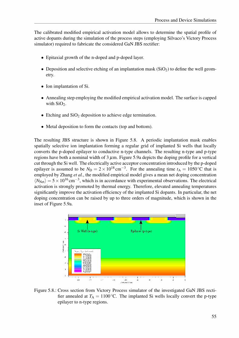
Process and Device Simulations
The calibrated modified empirical activation model allows to determine the spatial profile ofactive dopants during the simulation of the process steps (employing Silvaco’s Victory Processsimulator) required to fabricate the considered GaN JBS rectifier:
• Epitaxial growth of the n-doped and p-doped layer.
• Deposition and selective etching of an implantation mask (SiO2) to define the well geom-etry.
• Ion implantation of Si.
• Annealing step employing the modified empirical activation model. The surface is cappedwith SiO2.
• Etching and SiO2 deposition to achieve edge termination.
• Metal deposition to form the contacts (top and bottom).
The resulting JBS structure is shown in Figure 5.8. A periodic implantation mask enablesspatially selective ion implantation forming a regular grid of implanted Si wells that locallyconverts the p-doped epilayer to conductive n-type channels. The resulting n-type and p-typeregions have both a nominal width of 3 µm. Figure 5.9a depicts the doping profile for a verticalcut through the Si well. The electrically active acceptor concentration introduced by the p-dopedepilayer is assumed to be ND = 2×1018 cm−3. For the annealing time tA = 1050C that isemployed by Zhang et al., the modified empirical model gives a mean net doping concentration〈NNet〉= 5×1016 cm−3, which is in accordance with experimental observations. The electricalactivation is strongly promoted by thermal energy. Therefore, elevated annealing temperaturessignificantly improve the activation efficiency of the implanted Si dopants. In particular, the netdoping concentration can be raised by up to three orders of magnitude, which is shown in theinset of Figure 5.9a.
Figure 5.8.: Cross section from Victory Process simulator of the investigated GaN JBS recti-fier annealed at TA = 1100C. The implanted Si wells locally convert the p-typeepilayer to n-type regions.
55

Process and Device Simulations
(a) (b)
Figure 5.9.: (a) Doping depth profiles for the Si-implanted wells of the GaN JBS rectifiers. Thedashed line refers to the acceptor concentration of the p-type epilayer. Elevatedannealing temperatures TA enhance the activation of Si and thus increase the netdoping concentration NNet, as shown in the inset figure.(b) GaN JBS rectifier forward characteristics. The experimental device character-istics reported by Zhang et al. [86] is reproduced with high accuracy. Elevatedannealing temperatures allow to reduce the on-state resistance by approximatelyone order of magnitude (RTA=1060C
on ≈ 0.97mΩ, RTA=1300Con ≈ 0.58mΩ).
5.3.3. GaN JBS Rectifier Device Simulations
The JBS rectifier device simulations are also investigated using Silvaco’s Victory Device sim-ulator. As described in Section 5.2.3 the semi-classical drift-diffusion approach (5.1), (5.3),and (5.4) is employed. However, GaN differs from 4H-SiC in several carrier-transport relatedproperties. In contrast to 4H-SiC, incomplete ionization can be accurately described with thesingle-level model (5.8). In the recent literature [107], highly specialized models and parame-ters concerning generation/recombination, bandgap narrowing, and carrier mobility have beensummarized. The impurity concentration-dependent mobility for low electric fields is describedwith the Thomas Caughey model. For the high field mobility, the ’GaNsat High-Field MobilityModel’ proposed by Farahmand et al. [108] is available in Victory Device.
The JBS rectifier structure relies on two different types of metallic contacts: a Schottky contactat the anode and an Ohmic contact at the cathode. At Schottky contacts the Fermi level of themetal is not aligned with the quasi-Fermi level of the semiconductor (GaN). In Victory Devicethis is taken into account by including the Schottky barrier for the calculation of the potentialboundary condition (Dirichlet). The Schottky barrier is determined by the difference of themetal’s and semiconductor’s workfunction. For Ohmic contacts the Fermi levels are alignedand no Schottky barrier has to be overcome by the carriers. All employed models and theassociated parameters are summarized in Appendix B.
The simulation of the forward characteristics of the considered GaN JBS rectifier reproducesthe experimentally obtained forward voltage Von = 0.7V and the specific on-state resistance
56

Process and Device Simulations
Ron = 7.6mΩcm−2. Figure 5.9b illustrates the strong impact of the annealing temperatureon the device operation. Enhancing the annealing temperature from TA = 1050C to 1300Cresults in a decrease of the on-state resistance by one order of magnitude. The electrical ac-tivation efficiency passes from the weakly activated state (Ract < 0.05) through medium acti-vation to reach nearly full activation (Ract > 0.95) within a small annealing temperature band∆TA = 50C. This phenomenon has also been experimentally observed in implanted SiC [37],[85]. The empirical activation model is capable of describing this distinctive property, as il-lustrated in Figure 4.9. Furthermore, the characteristic high temperature saturation behavior ofactivation efficiency directly translates to a current saturation as the annealing temperatures areraised. The remarkable impact of the active dopant concentration on the actual device char-acteristics confirms the high relevance of modeling capabilities for semiconductor processingsteps, in particular post-implantation annealing.
57


6. Summary and Outlook
The wide-bandgap semiconductors SiC and gallium nitride GaN are highly attractive for ap-plication in power electronics due to their excellent material properties. However, both arechallenging for process technology, in particular due to the issues in ion implantation and thesubsequent thermal annealing steps, which strongly impact the final device’s operation. In or-der to achieve high electrical activation efficiency of implanted SiC and GaN, remarkably highannealing temperatures (SiC: > 1500C, GaN: > 1300C) are necessary. In the course ofthis thesis, the micro-physical mechanisms that define the electrical activation of implanted re-gions were investigated. The formation of native and impurity related point defect clusters andagglomerates were found to limit the activation efficiency for high implantation doses.
A comprehensive study of annealing experiments in the literature culminated in developing anempirical model that predicts the electrical activation efficiency as a function of the main pro-cess parameters, namely annealing temperature, annealing time, and implanted dopant concen-tration. The presented model was calibrated for implantation and annealing of 4H-SiC with theacceptor species Al and B and the donor species N and P. Si-implanted GaN exhibits reducedactivation efficiencies in the steady-state for low ( < 1017 cm−3) and moderate (≈ 1018 cm−3)doping concentrations. A modified activation model and its calibration, which accurately de-scribes this phenomenon, were presented and calibrated.
The activation models were incorporated into Silvaco’s Victory Process simulator, enablingthe optimization of the annealing parameters for semiconductor fabrication processes. Processsimulations were coupled with device simulations utilizing Silvaco’s Victory Device simulator,which allowed to investigate the full workflow of state-of-the-art power device structures: fromfabrication to determining the electrical characteristics. The impact of the annealing parame-ters on the electrical behavior of 4H-SiC DMOSFETs and GaN JBS rectifiers was examinedemploying process and device simulations: Annealing temperature and annealing time stronglyinfluence the threshold voltage of the 4H-SiC DMOSFET and is thus crucial for the final devicecharacteristics. The on-state resistance of a Si-implanted GaN JBS rectifier was found to be re-duced by more than one order of magnitude when employing elevated annealing temperatures.These results corroborate the high relevance of the annealing and the modeling capabilities ofthese fabrication steps and therefore underline this works importance.
Even though the empirical models predict the electrical activation with high accuracy, the micro-physical mechanisms associated with implantation damage and activation are not yet fully un-derstood for both GaN and SiC. Further investigations have to address the reasons for thereduced activation of Si-implanted GaN as well the generally low activation efficiency of accep-tors. Furthermore, the impact of the annealing ambient, self-diffusivity of C, and complex RTAtechniques on the activation processes of implanted SiC have to be examined. The simulationresults suggest that elevated annealing temperatures allow to significantly shorten the annealingtimes. However, this requires further improvements of the surface capping technology.
59

60

A. Modeling Parameters for SiCDMOSFETs
Table A.1.: Victory Device (VD) simulator setup for 4H-SiC-DMOSFETs.Model VD Statement VD Parameters Comment
General SetupDrift Diffusion (Default) (Default)
Fermi-Dirac Statistics MODELS FERMIDIRAC None
Two-Level Incomplete Ionization (Default for SiC) calibrated in VD Do not set INC.ION in MODELS
ContactsOhmic Contacts CONTACT VOLTAGE None
Lumped Contact ResistanceCONTACT
RESISTANCE=value OHMSvalue is fit parameter
Bandgap Modeling
Universal Energy Bandgap
Model (Varshni)(Default)
EG300 = 3.235
EGALPHA = 3.3e-2
EGBETA = 1e5
Parameters set in MATERIAL
Bandgap Narrowing MODELS BGN calibrated in VD
Mobility Modeling
Uhnevionak Combined Mobility Model
for 4H-SiC
MOBILITY ALTCVT.N
ALTCVT.P
calibrated in VD for electrons
MOBILITY:
ALT.N.DELTA = 1.5e12
ALT.P.MUBP1 = 125
ALT.P.MUBP2 = 0
ALT.P.MUMIN = 15.9
ALT.P.ALPHA = -0.5
ALT.P.EXP1 = -2.15
ALT.P.EXP3 = 1
ALT.P.EXP4 = 0.34
ALT.P.NREF = 1.76e19
Low Carrier + Transverse-Electric-Field
p values chosen to reproduce
Caughey Tomas Model
High-Field Mobility (Canali) MODELS FLDMOB
MATERIAL:
VSATN = 2.2e7
VSATP = 1.0e7
MOBILITY:
BETAN = 1.2
BETAP = 1.0
For simulations at T = 300 K
Anisotropic Mobility MOBILITY N.ANIOSTROPIC=1.2
Generation and Recombination
Shockley-Read-Hall MODELS SRHMATERIAL:
TAUN0 = 1e-9
TAUP0 = 1e-9
Auger Recombination MODELS AUGERMATERIAL:
AUGN = 1e-29
AUGP = 1e-29
Impact Ionization - Selberherr IMPACT SELBERHERR
IMPACT:
AN1 = 3.44e6, AN2 = 3.44e6
AP1 = 3.5e6, AP2 = 3.6e6
BN1 = 2.5e7, BN2 = 2.5e7
BP1 = 1.7e7, BP2 = 1.7e7
BETAN = 1.0 BETAP = 1.0
Interface Traps INTTRAP
ACCEPTOR:
DENSITY = 3e+12
DEGEN = 12
E.LEVEL=0.075
SIGN=1-14
SIGP=1e-14
One effective acceptor-like trap
61

B. Modeling Parameters for GaN JBSRectifiers
Table B.1.: Victory Device (VD) setup for GaN JBS rectifiers.Model VD Statement VD Parameters Comment
General SetupDrift Diffusion (Default) (Default)
Fermi-Dirac Statistics MODELS FERMIDIRAC None
Incomplete Ionization (Single level) MODELS INCOMPLETE
MATERIAL:
GCB=2
GVB=2
A.EAB=0.240
A.EDB=0.017
B.EAB=3.14e-8
B.EDB=3.4e-9
ContactsOhmic Contact CONTACT VOLTAGE None
Schottky Contact CONTACT WORKFUNCTION 5.25
Bandgap Modeling
Universal Energy Bandgap Model (Varshni) (Default)EG300 = 3.46
EGALPHA = 9.09e-4
EGBETA = 830
Parameters set in MATERIAL
Bandgap Narrowing BGN (Default)
Mobility Modeling
Caughey Thomas Model MODELS ANALYTIC
MOBILITY
ALPHAN.CAUG=-1.5
BETAN.CAUG=1.5
DELTAN.CAUG=0.81
GAMMAN.CAUG=3.02
MU1N.CAUG=115
MU2N.CAUG=1800
NCRITN.CAUG=7e16
ALPHAP.CAUG=2.0
BETAP.CAUG=-2.34
DELTAP.CAUG=-2.311
GAMMAP.CAUG=0.869
MU1P.CAUG=12.0
MU2P.CAUG=167
NCRITP.CAUG=3e17
Low field doping-dependent
High-Field Mobility for Electrons MOBILITY GANSAT.N (Calibrated in VD, only for electrons) GaNsat High-Field Mobility Model
High-Field Mobility for Holes MOBILITY FLDMOB.P
MOBILITY:
BETAP=0.725
MATERIAL:
VSATP=7e6
Caughey and Thomas High Field Model
Generation and Recombination
Shockley-Read-Hall MODELS SRHMATERIAL:
TAUN0=0.7e-9
TAUP0=2e-9
Auger Recombination MODELS AUGERMATERIAL:
AUGN=3e-31
AUGP=3e-31
62

Bibliography
[1] M. Tanenbaum, L. B. Valdes, E. Buehler, and N. B. Hannay. “Silicon n-p-n GrownJunction Transistors”. J. Appl. Phys. 26.6 (1955), pp. 686–692. DOI:10.1063/1.1722071.
[2] T. Kimoto and J. A. Cooper. Fundamentals of Silicon Carbide Technology: Growth,Characterization, Devices and Applications. 2014, pp. 1–538. DOI:10.1002/9781118313534.
[3] T. J. Flack, B. N. Pushpakaran, and S. B. Bayne. “GaN Technology for PowerElectronic Applications: A Review”. J. Electron. Mater. 45.6 (2016), pp. 2673–2682.DOI: 10.1007/s11664-016-4435-3.
[4] S. Pimputkar, J. S. Speck, S. P. Denbaars, and S. Nakamura. “Prospects for LEDLighting”. Nat. Photonics 3.4 (2009), pp. 180–182. ISSN: 17494885. DOI:10.1038/nphoton.2009.32.
[5] R. Quay. Gallium Nitride Electronics. Springer Science & Business Media, 2008.
[6] O. Ambacher, J. Smart, J. R. Shealy, N. G. Weimann, K. Chu, M. Murphy,W. J. Schaff, L. F. Eastman, R. Dimitrov, L. Wittmer, M. Stutzmann, W. Rieger, andJ. Hilsenbeck. “Two-dimensional Electron Gases Induced by Spontaneous andPiezoelectric Polarization Charges in N- and Ga-face AlGaN/GaN Heterostructures”.J. Appl. Phys. 85.6 (1999), p. 3222. DOI: 10.1063/1.369664.
[7] O. Ambacher, B. Foutz, J. Smart, J. Shealy, N. Weimann, K. Chu, M. Murphy,A. Sierakowski, W. Schaff, L. Eastman, R. Dimitrov, A. Mitchell, and M. Stutzmann.“Two Dimensional Electron Gases Induced by Spontaneous and PiezoelectricPolarization in Undoped and Doped AlGaN/GaN Heterostructures”. Appl. Phys. Lett.87.1 (2000), p. 334. DOI: 10.1063/1.371866.
[8] F. Bernardini, V. Fiorentini, and D. Vanderbilt. “Spontaneous Polarization andPiezoelectric Constants of III-V Nitrides”. Phys. Rev. B 56.16 (1997),pp. R10024–R10027. DOI: 10.1103/PhysRevB.56.R10024.
[9] S. C. Jain, M. Willander, J. Narayan, and R. V. Overstraeten. “III–Nitrides: Growth,Characterization, and Properties”. J. Appl. Phys. 87.3 (2000), pp. 965–1006. DOI:10.1063/1.371971.
[10] C Ronning, E. P. Carlson, and R. F. Davis. “Ion Implantation into Gallium Nitride”.Phys. Rep. 351.5 (2001), pp. 349–385. DOI: 10.1016/S0370-1573(00)00142-3.
[11] T. Paskova, D. A. Hanser, and K. R. Evans. “GaN Substrates for III-Nitride Devices”.Proc. IEEE 98.7 (2010), pp. 1324–1338. DOI: 10.1109/JPROC.2009.2030699.
[12] D. Ehrentraut and T. Fukuda. “The Ammonothermal Crystal Growth of GalliumNitride - a Technique on the Up Rise”. Proc. IEEE 98.7 (2010), pp. 1316–1323. DOI:10.1109/JPROC.2009.2029878.
63

Bibliography
[13] M Bockowski, M Iwinska, M Amilusik, M Fijalkowski, B Lucznik, and T Sochacki.“Challenges and Future Perspectives in HVPE-GaN Growth on Ammonothermal GaNSeeds”. Semicond. Sci. Technol. 31.9 (2016), p. 093002. DOI:10.1088/0268-1242/31/9/093002.
[14] H. Amano, N. Sawaki, I. Akasaki, and Y. Yoyoda. “Metalorganic Vapor PhaseEpitaxial Growth of a High Quality GaN Film Using an AlN Buffer Layer”. Appl.Phys. Lett. 48.1986 (1986), pp. 353–355. DOI: 10.1063/1.96549.
[15] J Roy, S Chandra, S Das, and S Maitra. “Oxidation Behaviour of Silicon Carbide - aReview”. Rev. Adv. Mater. Sci 38 (2014), pp. 29–39. DOI:10.1016/j.jnucmat.2007.05.016.
[16] T. Hiyoshi, T. Masuda, K. Wada, S. Harada, T. Tsuno, and Y. Namikawa. “SiC HighChannel Mobility MOSFET”. SEI Tech. Rev. 77 (2013), pp. 122–126.
[17] V. Uhnevionak, A. Burenkov, C. Strenger, G. Ortiz, E. Bedel-Pereira, V. Mortet,F. Cristiano, A. J. Bauer, and P. Pichler. “Comprehensive Study of the ElectronScattering Mechanisms in 4H-SiC MOSFETs”. IEEE Trans. Electron Devices 62.8(2015), pp. 2562–2570. DOI: 10.1109/TED.2015.2447216.
[18] T. Tsuchiya and P. M. Lenahan. “Distribution of the Energy Levels of IndividualInterface Traps and a Fundamental Refinement in Charge Pumping Theory”. Jpn. J.Appl. Phys. 56.3 (2017), p. 031301. DOI: 10.7567/JJAP.56.031301.
[19] V. Simonka, A. Hossinger, J. Weinbub, and S. Selberherr. “Growth Rates of DryThermal Oxidation of 4H-Silicon Carbide”. J. Appl. Phys. 120.13 (2016), p. 135705.DOI: 10.1063/1.4964688.
[20] T. Yamada, J. Ito, R. Asahara, K. Watanabe, M. Nozaki, S. Nakazawa, Y. Anda,M. Ishida, T. Ueda, A. Yoshigoe, T. Hosoi, T. Shimura, and H. Watanabe.“Comprehensive Study on Initial Thermal Oxidation of GaN(0001) Surface andSubsequent Oxide Growth in Dry Oxygen Ambient”. J. Appl. Phys. 121.3 (2017),p. 035303. DOI: 10.1063/1.4974458.
[21] L. Ma, K. F. Adeni, C. Zeng, Y. Jin, K. Dandu, Y. Saripalli, and D. Barlage.“Comparison of Different GaN Etching Techniques”. CS MANTECH Conf. (2006),pp. 105–108.
[22] M. Niibe, T. Kotaka, R. Kawakami, T. Inaoka, K. Tominaga, and T. Mukai. “DamageAnalysis of Plasma-Etched n-GaN Crystal Surface by Nitrogen K Near-Edge X-rayAbsorption Fine Structure Spectroscopy”. Jpn. J. Appl. Phys. 51 (2012), 01AB02. DOI:10.1143/JJAP.51.01AB02.
[23] T. Grasser. Modeling of Semiconductor Devices. Lecture Notes, 2015.
[24] S. O. Kucheyev, J. S. Williams, and S. J. Pearton. “Ion Implantation into GaN”. Mater.Sci. Eng. R Reports 33.2-3 (2001), pp. 51–107. DOI:10.1016/S0927-796X(01)00028-6.
[25] M. Kondow and T. Kitatani. “In Situ Annealing of GaInNAs up to 600C”. Japanese J.Appl. Physics, Part 1 Regul. Pap. Short Notes Rev. Pap. 40.1 (2001), pp. 108–109.ISSN: 00214922.
[26] H. Morkoc. Handbook of Nitride Semiconductors and Devices, Materials Properties,Physics and Growth. John Wiley & Sons, 2009.
64
Bibliography
[27] R. G. Elliman and J. S. Williams. “Advances in Ion Beam Modification ofSemiconductors”. Curr. Opin. Solid State Mater. Sci. 19.1 (2015), pp. 49–67. DOI:10.1016/j.cossms.2014.11.007.
[28] T Zhu and R. A. Oliver. “Unintentional Doping in GaN”. Phys. Chem. Chem. Phys.14.27 (2012), pp. 9558–9573. DOI: 10.1039/c2cp40998d.
[29] J. L. Lyons and C. G. Van de Walle. “Computationally Predicted Energies andProperties of Defects in GaN”. npj Comput. Mater. 3.1 (2017), p. 12. DOI:10.1038/s41524-017-0014-2.
[30] S. J. Pearton, C. B. Vartuli, J. C. Zolper, C. Yuan, and R. A. Stall. “Ion ImplantationDoping and Isolation of GaN”. Appl. Phys. Lett. 67.1995 (1995), p. 1435. DOI:10.1063/1.114518.
[31] S. J. Pearton, J. C. Zolper, R. J. Shul, and F. Ren. “GaN: Processing, Defects, andDevices”. J. Appl. Phys. 86.1 (1999), pp. 1–78. DOI: 10.1063/1.371145.
[32] H. Amano, M. Kito, K. Hiramatsu, and I. Akasaki. “P-Type Conduction in Mg-DopedGaN Treated with Low-Energy Electron Beam Irradiation (LEEBI) ”. Jpn. J. Appl.Phys. 28.Part 2, No. 12 (1989), pp. L2112–L2114. DOI: 10.1143/JJAP.28.L2112.
[33] S. A. Campbell. The Science and Engineering of Microelectronic Fabrication. OxfordUniversity Press, USA, 1996.
[34] C. Ostermaier, S. I. Ahn, K. Potzger, M. Helm, J. Kuzmik, D. Pogany, G. Strasser,J. H. Lee, S. H. Hahm, and J. H. Lee. “Study of Si Implantation into Mg-doped GaNfor MOSFETs”. Phys. Status Solidi Curr. Top. Solid State Phys. 7.7-8 (2010),pp. 1964–1966. DOI: 10.1002/pssc.200983534.
[35] B. N. Feigelson, T. J. Anderson, M. Abraham, J. A. Freitas, J. K. Hite, C. R. Eddy, andF. J. Kub. “Multicycle Rapid Thermal Annealing Technique and its Application for theElectrical Activation of Mg implanted in GaN”. J. Cryst. Growth 350.1 (2012),pp. 21–26. DOI: 10.1016/j.jcrysgro.2011.12.016.
[36] J. A. Fellows, Y. K. Yeo, R. L. Hengehold, and D. K. Johnstone. “Electrical ActivationStudies of GaN Implanted with Si from Low to High Dose”. Appl. Phys. Lett. 80.11(2002), pp. 1930–1932. DOI: 10.1063/1.1458694.
[37] Y. Irokawa, O. Fujishima, T. Kachi, and Y. Nakano. “Electrical ActivationCharacteristics of Silicon-Implanted GaN”. J. Appl. Phys. 97.8 (2005), pp. 1–6. DOI:10.1063/1.1863458.
[38] Y. Niiyama, S. Ootomo, J. Li, H. Kambayashi, T. Nomura, S. Yoshida, K. Sawano, andY. Shiraki. “Si Ion Implantation into Mg-doped GaN for Fabrication of ReducedSurface Field Metal-Oxide-Semiconductor Field-Effect Transistors”. Jpn. J. Appl.Phys. 47.7 PART 1 (2008), pp. 5409–5416. DOI: 10.1143/JJAP.47.5409.
[39] I. C. Kizilyalli, A. P. Edwards, O. Aktas, T. Prunty, and D. Bour. “Vertical Power p-nDiodes Based on bulk GaN”. IEEE T. Electron Dev. 62.2 (2015), pp. 414–422. DOI:10.1109/TED.2014.2360861.
[40] T. J. Anderson, J. D. Greenlee, B. N. Feigelson, J. K. Hite, K. D. Hobart, and F. J. Kub.“Improvements in the Annealing of Mg Ion Implanted GaN and Related Devices”.IEEE T. Semiconduct. M. 29.4 (2016), pp. 343–348. DOI: 10.1109/TSM.2016.2600371.
65

Bibliography
[41] J. Neugebauer and C. G. Van de Walle. “Hydrogen in GaN: Novel Aspects of aCommon Impurity”. Phys. Rev. Lett. 75.24 (1995), pp. 4452–4455. DOI:10.1103/PhysRevLett.75.4452.
[42] C. G. Van De Walle and J. Neugebauer. “First-principles Calculations for Defects andImpurities: Applications to III-Nitrides”. J. Appl. Phys. 95.8 (2004), pp. 3851–3879.DOI: 10.1063/1.1682673.
[43] T. Niwa, T. Fujii, and T. Oka. “High Carrier Activation of Mg Ion-Implanted GaN byConventional Rapid Thermal Annealing”. Appl. Phys. Express 10.091002 (2017),p. 091002. DOI: 10.7567/APEX.10.091002.
[44] J. D. Hwang and G. H. Yang. “Activation of Mg-doped P-GaN by Using Two-Stepannealing”. Appl. Surf. Sci. 253.10 (2007), pp. 4694–4697. DOI:10.1016/j.apsusc.2006.10.026.
[45] T. J. Anderson, B. N. Feigelson, F. J. Kub, M. J. Tadjer, K. D. Hobart, M. A. Mastro,J. K. Hite, and C. R. Eddy. “Activation of Mg Implanted in GaN by Multicycle RapidThermal Annealing”. Electron. Lett. 50.3 (2014), pp. 197–198. DOI:10.1049/el.2013.3214.
[46] K. Nomoto, K. Takahasi, H. Oikawa, and T. Nishimura. “Ion Implantation into GaNand Implanted GaN Power Transistors”. ECS Trans. 69.11 (2015), pp. 105–112. DOI:10.1149/06911.0105ecst.
[47] B. J. Baliga. “Gallium Nitride Devices for Power Electronic Applications”. Semicond.Sci. Technol. 28.7 (2013). DOI: 10.1088/0268-1242/28/7/074011.
[48] J Shealy, J Smart, M Poulton, R Sadler, D Grider, S Gibb, B Hosse, B Sousa,D Halchin, V Steel, P Garber, P Wilkerson, B Zaroff, J Dick, T Mercier, J Bonaker,M Hamilton, C Greer, and M Isenhour. “Gallium Nitride (GaN) HEMT’s: Progressand Potential for Commercial Applications”. 24th Annu. Tech. Dig. Gall. ArsenideIntegr. Circuit (GaAs IC) Symp. (2002), pp. 243–246.
[49] A. Sciuto, F. Roccaforte, S. Di Franco, V. Raineri, and G. Bonanno. “HighResponsivity 4H-SiC Schottky UV Photodiodes Based on the Pinch-off SurfaceEffect”. Appl. Phys. Lett. 89.8 (2006), pp. 3–6. DOI: 10.1063/1.2337861.
[50] B. S. Nakamura and M. R. Krames. “History of Gallium – Nitride-BasedLight-Emitting Diodes for Illumination”. Proc. IEEE (2013), pp. 1–10. DOI:10.1109/JPROC.2013.2274929.
[51] Class for Physics of the Royal Swedish Academy of Sciences. Efficient BlueLight-emitting Diodes Leading to Bright and Energy-saving White Light Sources.2014. URL: https://www.nobelprize.org/nobel prizes/physics/laureates/2014/.
[52] G. Fasching. Werkstoffe fur die Elektrotechnik. 4th Edition. Springer, 2005.
[53] A. Uedono, S. Takashima, M. Edo, K. Ueno, H. Matsuyama, H. Kudo, H. Naramoto,and S. Ishibashi. “Vacancy-type Defects and Their Annealing Behaviors inMg-implanted GaN Studied by a Monoenergetic Ppositron Beam”. Phys. Status SolidiB. 252.12 (2015), pp. 2794–2801. DOI: 10.1002/pssb.201552345.
[54] LAMMPS Molecular Dynamics Simulator. http://lammps.sandia.gov/. Accessed:5/3/2018.
66

Bibliography
[55] B.-C. Chung and M. Gershenzon. “The Influence of Oxygen on the Electrical andOptical Properties of GaN Crystals Grown by Metalorganic Vapor Phase Epitaxy”. J.Appl. Phys. 72.2 (1992), pp. 651–659. DOI: 10.1063/1.351848.
[56] P. Perlin, T. Suski, H. Teisseyre, M. Leszczynski, I. Grzegory, J. Jun, S. Porowski,P. Bogusławski, J. Bernholc, J. C. Chervin, A. Polian, and T. D. Moustakas. “Towardsthe Identification of the Dominant Donor in GaN”. Phys. Rev. Lett. 75.2 (1995),pp. 296–299. DOI: 10.1103/PhysRevLett.75.296.
[57] J. Neugebauer and C. G. Van de Walle. “Theory of Point Defects and Complexes inGaN”. MRS Proceedings 395 (1995), p. 645. DOI: 10.1557/PROC-395-645.
[58] S Nakamura and B Gil. “Group III Nitride Semiconductor Compounds”. Oxford Sci.Publ. (1998), p. 391.
[59] K. Kojima, S. Takashima, M. Edo, K. Ueno, M. Shimizu, T. Takahashi, S. Ishibashi,A. Uedono, and S. F. Chichibu. “Nitrogen Vacancies as a Common Element of theGreen Luminescence and Nonradiative Recombination Centers in Mg-implanted GaNlayers Formed on a GaN Substrate”. Applied Physics Express 10.6 (2017), p. 061002.DOI: 10.7567/APEX.10.061002.
[60] P. Boguslawski, E. L. Briggs, and J. Bernholc. “Amphoteric Properties ofSubstitutional Carbon Impurity in GaN and AlN”. Appl. Phys. Lett. 69.2 (1996),p. 233. DOI: 10.1063/1.117934.
[61] S. Nakamura, T. Mukai, S. Masayuki, and N. Iwasa. “Thermal Annealing Effects onP-Type Mg-Doped GaN Films”. Jpn. J. Appl. Phys. 31 (1992), pp. L139–L142. DOI:10.1143/JJAP.31.L139.
[62] R. Nipoti, A. Canera, G. Alferi, and L. Kranz. “About the Electrical Activation of 1e20cmˆ-3 Ion Implanted Al in 4H–SiC at Annealing Temperatures in the Range1500-1950C”. Proc. Int. Conf. Silicon Carbide Relat. Mater. in print (2017).
[63] P. Fastenko. “Modeling and Simulation of Arsenic Activation and Diffusion inSilicon”. PhD thesis. University of Washington, 2002.
[64] P. M. Fahey, P. B. Griffin, and J. D. Plummer. “Point Defects and Dopant Diffusion inSilicon”. Rev. Mod. Phys. 61.2 (1989), pp. 289–384. DOI:10.1103/RevModPhys.61.289.
[65] E. L. Cussler. Diffusion: Mass Transfer in Fluid Systems. Cambridge University Press,2009. DOI: 10.1017/CBO9780511805134.010.
[66] R. B. Fair. “A Quantitative Model for the Diffusion of Phosphorus in Silicon and theEmitter Dip Effect”. J. Electrochem. Soc. 124.7 (1977), p. 1107. DOI:10.1149/1.2133492.
[67] H. Z. Massoud. “Thermal Oxidation of Silicon in Dry Oxygen Growth-RateEnhancement in the Thin Regime”. J. Electrochem. Soc. 132.11 (1985), p. 2685. DOI:10.1149/1.2113648.
[68] L. J. van der Pauw. “A Method of Measuring the Resistivity and Hall Coefficient onLamellae of Arbitrary Shape”. Philips Tech. Rev. 20 (1958), pp. 220–224.
[69] A. Parisini and R. Nipoti. “Analysis of the Hole Transport through Valence BandStates in Heavy Al Doped 4H-SiC by Ion Implantation”. J. Appl. Phys. 114.24 (2013),p. 243703. DOI: 10.1063/1.4852515.
67

Bibliography
[70] V. Simonka, A. Hossinger, J. Weinbub, and S. Selberherr. “Empirical Model forElectrical Activation of Aluminum- and Boron-Implanted Silicon Carbide”. IEEE T.Electron Dev. 65.2 (2018), pp. 674–679. DOI: DOI:10.1109/TED.2017.2786086.
[71] A Benninghoven. “Surface Investigation of Solids by the Statical Method of SecondaryIon Mass Spectroscopy (SIMS)”. Surf. Sci. 35 (1973), pp. 427–457. DOI:10.1016/0039-6028(73)90232-X.
[72] T. Tsirimpis, M. Krieger, H. B. Weber, and G. Pensl. “Electrical Activation of B+-IonsImplanted into 4H-SiC”. Mater. Sci. Forum 645-648 (2010), pp. 697–700. DOI:10.4028/www.scientific.net/MSF.645-648.697.
[73] N. S. Saks, A. K. Agarwal, S. H. Ryu, and J. W. Palmour. “Low-dose Aluminum andBoron Implants in 4H and 6H Silicon Carbide”. J. Appl. Phys. 90.6 (2001),pp. 2796–2805. DOI: 10.1063/1.1392958.
[74] M. Laube, F. Schmid, G. Pensl, G. Wagner, M. Linnarsson, and M. Maier. “ElectricalActivation of High Concentrations of N+ and P+ Ions Implanted into 4H–SiC”. J.Appl. Phys. 92.1 (2002), p. 549. DOI: 10.1063/1.1479462.
[75] N. S. Saks, S. H. Ryu, and A. V. Suvorov. “Low-dose n-type Nitrogen Implants in4H-SiC”. Appl. Phys. Lett. 81.26 (2002), pp. 4958–4960. DOI: 10.1063/1.1531838.
[76] S. Blanque, R. Perez, P. Godignon, N. Mestres, E. Morvan, A. Kerlain, C. Dua,C. Brylinski, M. Zielinski, and J. Camassel. “Room Temperature Implantation andActivation Kinetics of Nitrogen and Phosphorus in 4H-SiC Crystals”. Mater. Sci.Forum 457-460 (2004), pp. 893–896. DOI:10.4028/www.scientific.net/MSF.457-460.893.
[77] M. A. Capano, J. A. Cooper, M. R. Melloch, A. Saxler, and W. C. Mitchel. “IonizationEnergies and Electron Mobilities in Phosphorus- and Nitrogen-implanted 4H-SiliconCarbide”. J. Appl. Phys. 87.12 (2000), pp. 8773–8777. DOI: 10.1063/1.373609.
[78] T Kimoto, O Takemura, H Matsunami, T Nakata, and M Inoue. “A+ and B+
Implantations into 6H-SiC Epilayers and Application to pn Junction Diodes”. J.Electron. Mater. 27.4 (1998), pp. 358–364. DOI: 10.1007/s11664-998-0415-6.
[79] S. G. Sundaresan, M. V. Rao, Y.-l. Tian, M. C. Ridgway, J. A. Schreifels, andJ. J. Kopanski. “Ultrahigh-temperature Microwave Annealing of Al+-andP+-Implanted 4H-SiC”. J. Appl. Phys. 101.7 (2007), p. 73708. DOI:10.1063/1.2717016.
[80] W. Hailei, S. Guosheng, Y. Ting, Y. Guoguo, W. Lei, Z. Wanshun, L. Xingfang,Z. Yiping, and W. Jialiang. “Effect of Annealing Process on the Surface Roughness inMultiple Al Implanted 4H-SiC”. J. Semicond. 32.7 (2011), p. 72002. DOI:10.1088/1674-4926/32/7/072002.
[81] R. Nipoti, R. Scaburri, A. Hallen, and A. Parisini. “Conventional Thermal Annealingfor a more Efficient p-type Doping of Al+ Implanted 4H-SiC”. J. Mater. Res. 28.1(2013), pp. 17–22. DOI: 10.1557/jmr.2012.207.
[82] J. Senzaki, K. Fukuda, and K. Arai. “Influences of Postimplantation AnnealingConditions on Resistance Lowering in High-Phosphorus-Implanted 4H-SiC”. J. Appl.Phys. 94.5 (2003), pp. 2942–2947. DOI: 10.1063/1.1597975.
68
Bibliography
[83] T. Troffer, C. Peppermuller, G. Pensl, K. Rottner, and A. Schoner.“Phosphorus-Related Donors in 6H-SiC Generated by Ion Implantation”. J. Appl.Phys. 80.7 (1996), p. 3739. DOI: 10.1063/1.363325.
[84] T. Kimoto, N. Inoue, and H. Matsunami. “Nitrogen Ion Implantation into α-SiCEpitaxial Layers”. Phys. Status Solidi A. 162.1 (1997), pp. 263–276. DOI:10.1002/1521-396X(199707)162:1〈263::AID-PSSA263〉3.0.CO;2-W.
[85] C. E. Hager, K. A. Jones, M. A. Derenge, and T. S. Zheleva. “Activation of IonImplanted Si in GaN using a Dual AlN Annealing Cap”. J. Appl. Phys. 105.3 (2009).DOI: 10.1063/1.3068317.
[86] Y. Zhang, Z. Liu, M. J. Tadjer, M. Sun, D. Piedra, C. Hatem, T. J. Anderson,L. E. Luna, A. Nath, A. D. Koehler, H. Okumura, J. Hu, X. Zhang, X. Gao,B. N. Feigelson, K. D. Hobart, and T. Palacios. “Vertical GaN Junction BarrierSchottky Rectifiers by Selective Ion Implantation”. IEEE Electron Dev. Lett. 38.8(2017), pp. 1097–1100. DOI: 10.1109/LED.2017.2720689.
[87] A. K. Galwey and M. E. Brown. “Application of the Arrhenius Equation to Solid StateKinetics: Can this be Justified?” Thermochim. Acta 386.1 (2002), pp. 91–98. DOI:10.1016/S0040-6031(01)00769-9.
[88] K. Madsen and H. Nielsen. Introduction to Optimization and Data Fitting. Accessed:4/3/2018. Lecture Notes, 2010. URL:www2.imm.dtu.dk/pubdb/views/edoc download.php/5938/pdf/imm5938.pdf.
[89] L. Wilson. “International Technology Roadmap for Semiconductors (ITRS)”.Semicond. Ind. Assoc. (2013).
[90] R. W. Dutton. “Perspectives on Technology and Technology-Driven CAD”. IEEE T.Comput. Aid. D. 19.12 (2000), pp. 1544–1560. DOI: 10.1109/43.898831.
[91] Silvaco. Victory Process User’s Manual. 2017. URL: https://www.silvaco.com/.
[92] I. R. Chakarov and R. P. Webb. “Crystal-binary Collision Simulation of AtomicCollisions and Dynamic Damage Buildup in Crystalline Silicon”. Radiat. Eff. DefectsSolids 130.1 (1994), pp. 447–452. DOI: 10.1080/10420159408219802.
[93] T. Grasser, T. W. Tang, H. Kosina, and S. Selberherr. “A Review of Hydrodynamic andEnergy-Transport Models for Semiconductor Device Simulation”. Proc. IEEE 91.2(2003), pp. 251–273. DOI: 10.1109/JPROC.2002.808150.
[94] M. Bakowski, U. Gustafsson, and U. Lindefelt. “Simulation of SiC High PowerDevices”. Phys. Status Solidi A. 162.1 (1997), pp. 421–440. DOI:10.1002/1521-396X(199707)162:1〈421::AID-PSSA421〉3.0.CO;2-B.
[95] T. Ayalew. “SiC Semiconductor Devices Technology, Modeling, and Simulation”.PhD thesis. Technische Universitat Wien, 2004.
[96] Silvaco. Victory Device User’s Manual. 2017. URL: https://www.silvaco.com/.
[97] G. Xiao, J. Lee, J. J. Liou, and A. Ortiz-Conde. “Incomplete Ionization in aSemiconductor and its Implications to Device Modeling”. Microelectron. Reliab. 39.8(1999), pp. 1299–1303. DOI: 10.1016/S0026-2714(99)00027-X.
[98] M. Lades. “Modeling and Simulation of Wide Bandgap Semiconductor Devices :4H/6H-SiC”. PhD thesis. Technische Universitat Munchen, 2000.
69

Bibliography
[99] S. H. Ryu, S. Krishnaswami, M. O’Loughlin, J. Richmond, A. Agarwal, J. Palmour,and A. R. Hefner. “10-kV, 123-mΩ·cm2 4H-SiC Power DMOSFETs”. IEEE ElectronDev. Lett. 25.8 (2004), pp. 556–558. DOI: 10.1109/LED.2004.832122.
[100] R. S. Howell, S. Buchoff, S. Van Campen, T. R. McNutt, A. Ezis, B. Nechay,C. F. Kirby, M. E. Sherwin, R. C. Clarke, and R. Singh. “A 10-kV Large-Area 4H-SiCPower DMOSFET with Stable Subthreshold Behavior Independent of Temperature”.IEEE T. Electron Dev. 55.8 (2008), pp. 1807–1815. DOI: 10.1109/TED.2008.928204.
[101] L. Di Benedetto, G. D. Licciardo, T. Erlbacher, A. J. Bauer, and A. Rubino.“Optimized Design for 4H-SiC Power DMOSFET”. IEEE Electron Dev. Lett. 37.11(2016), pp. 1454–1457. DOI: 10.1109/LED.2016.2613821.
[102] A. Saha and J. A. Cooper. “A 1-kV 4H-SiC Power DMOSFET Optimized for LowON-Resistance”. IEEE T. Electron Dev. 54.10 (2007), pp. 2786–2791. DOI:10.1109/TED.2007.904577.
[103] M. Reisch. Elektronische Bauelemente: Funktion, Grundschaltungen, Modellierungmit SPICE. Springer, 2007. DOI: 10.1007/978-3-540-34015-7.
[104] S. M. Sze. Physics of Semiconductor Devices. New Jersey: John Wiley & Sons, 2007.DOI: 10.1002/9780470068328.
[105] W. Shockley and W. T. Read. “Statistics of the Recombination of Holes and Electrons”.Phys. Rev. 87.46 (1952), pp. 835–842. DOI: dx.doi.org/10.1103/PhysRev.87.835.
[106] B. J. Baliga. “The Pinch Rectifier: A Low-Forward-Drop High-Speed Power Diode”.IEEE Electron Dev. Lett. 5.6 (1984), pp. 194–196. DOI: 10.1109/EDL.1984.25884.
[107] G. Sabui, P. J. Parbrook, M. Arredondo-Arechavala, and Z. J. Shen. “Modeling andSimulation of Bulk Gallium Nitride Power Semiconductor Devices”. AIP Adv. 6.5(2016), p. 055006. DOI: 10.1063/1.4948794.
[108] M. Farahmand, C. Garetto, E. Bellotti, K. Brennan, M. Goano, E. Ghillino, G. Ghione,J. Albrecht, and P. Ruden. “Monte Carlo Simulation of Electron Transport in theIII-Nitride Wurtzite Phase Materials System: Binaries and Ternaries”. IEEE T.Electron Dev. 48.3 (2001), pp. 535–542. DOI: 10.1109/16.906448.
70

Own Publications
Journal Articles
[1] V. Simonka, A. Toifl, A. Hossinger, S. Selberherr, and J. Weinbub. ”Transient Modelfor Electrical Activation of Aluminium and Phosphorus-Implanted Silicon Carbide”.Journal of Applied Physics (2018), accepted.
Conference Contributions
[1] A. Toifl, V. Simonka, A. Hossinger, S. Selberherr, and J. Weinbub. ”Steady-StateEmpirical Model for Electrical Activation of Silicon-Implanted Gallium Nitride”. In-ternational Conference on Simulation of Semiconductor Processes and Devices (SIS-PAD) (2018), submitted.
[2] A. Toifl, V. Simonka, A. Hossinger, S. Selberherr, and J. Weinbub. ”Effects of Post-Implantation Annealing on Silicon Carbide DMOSFET Characteristics”. Interna-tional Conference on Solid State Devices and Materials (SSDM) (2018), submitted.
71


Erklarung
Hiermit erklare ich, dass die vorliegende Arbeit gemaß dem Code of Conduct, insbesonde-re ohne unzulassige Hilfe Dritter und ohne Benutzung anderer als der angegebenen Hilfsmittel,angefertigt wurde. Die aus anderen Quellen direkt oder indirekt ubernommenen Daten und Kon-zepte sind unter Angabe der Quelle gekennzeichnet. Die Arbeit wurde bisher weder im In- nochim Ausland in gleicher oder in ahnlicher Form in anderen Prufungsverfahren vorgelegt.
Wien, 22.5.2018
Alexander Toifl