Microelectronic Circuits 5th Edition (manual) By Sedra Smith.pdf
Microelectronic Circuits, Sixth Edition Sedra/Smith Copyright © 2010 by Oxford University Press, Inc.
C H A P T E R 4
Diodes
(non-linear devices)
Microelectronic Circuits, Sixth Edition Sedra/Smith Copyright © 2010 by Oxford University Press, Inc.
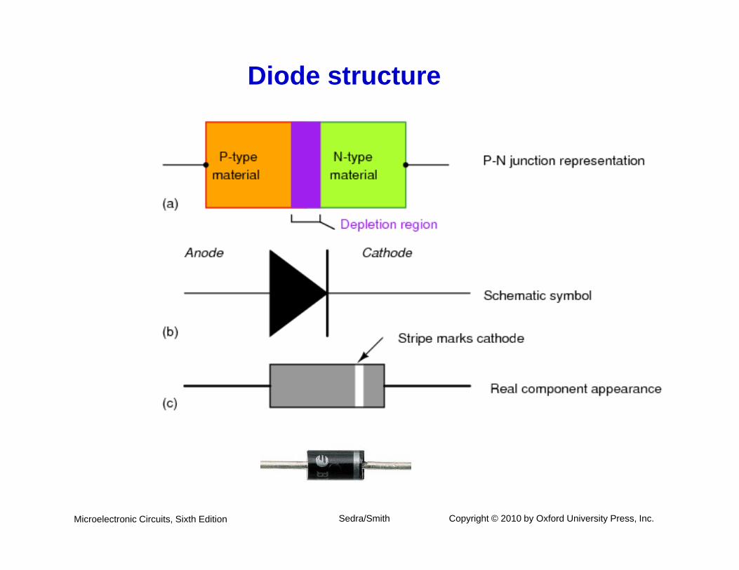
Diode structure
Microelectronic Circuits, Sixth Edition Sedra/Smith Copyright © 2010 by Oxford University Press, Inc.
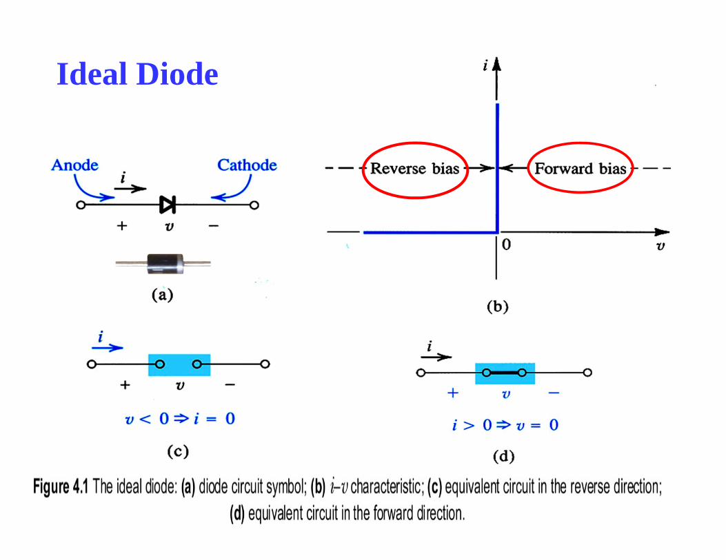
Ideal Diode
Microelectronic Circuits, Sixth Edition Sedra/Smith Copyright © 2010 by Oxford University Press, Inc.
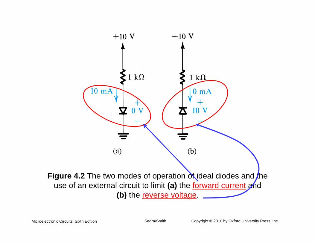
Figure 4.2 The two modes of operation of ideal diodes and the use of an external circuit to limit (a) the forward current and
(b) the reverse voltage.
Microelectronic Circuits, Sixth Edition Sedra/Smith Copyright © 2010 by Oxford University Press, Inc.
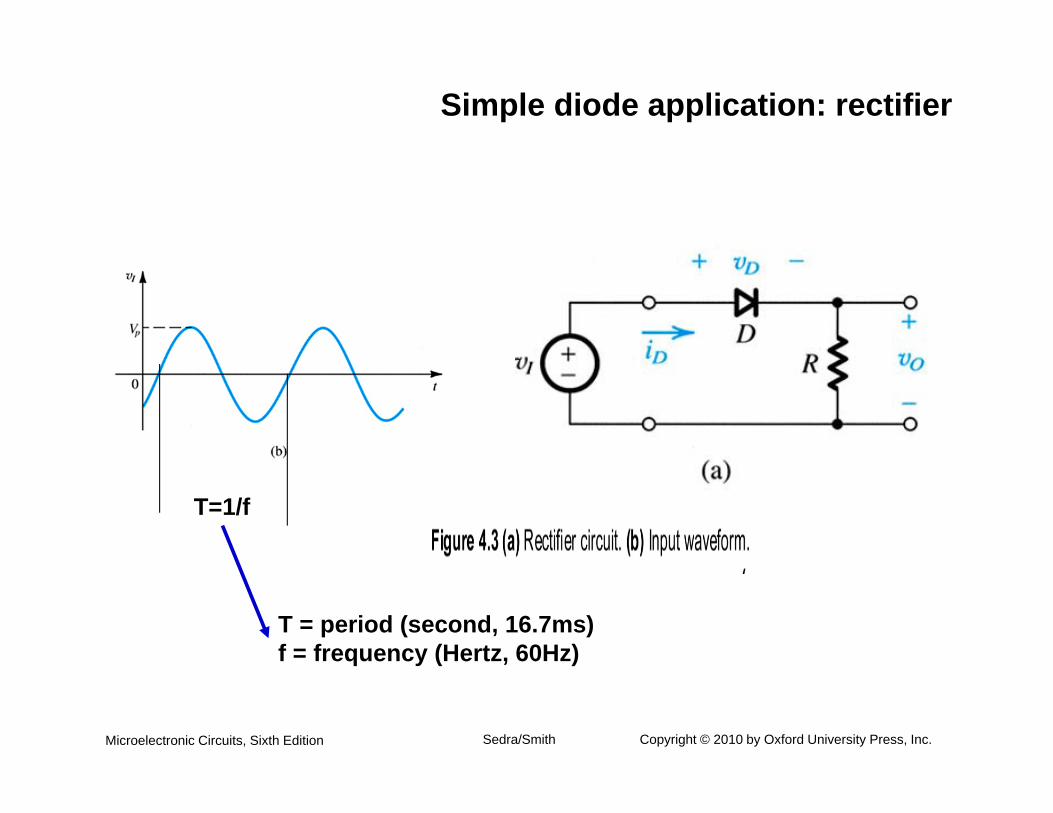
Simple diode application: rectifier
T=1/f
T = period (second, 16.7ms)f = frequency (Hertz, 60Hz)
Microelectronic Circuits, Sixth Edition Sedra/Smith Copyright © 2010 by Oxford University Press, Inc.
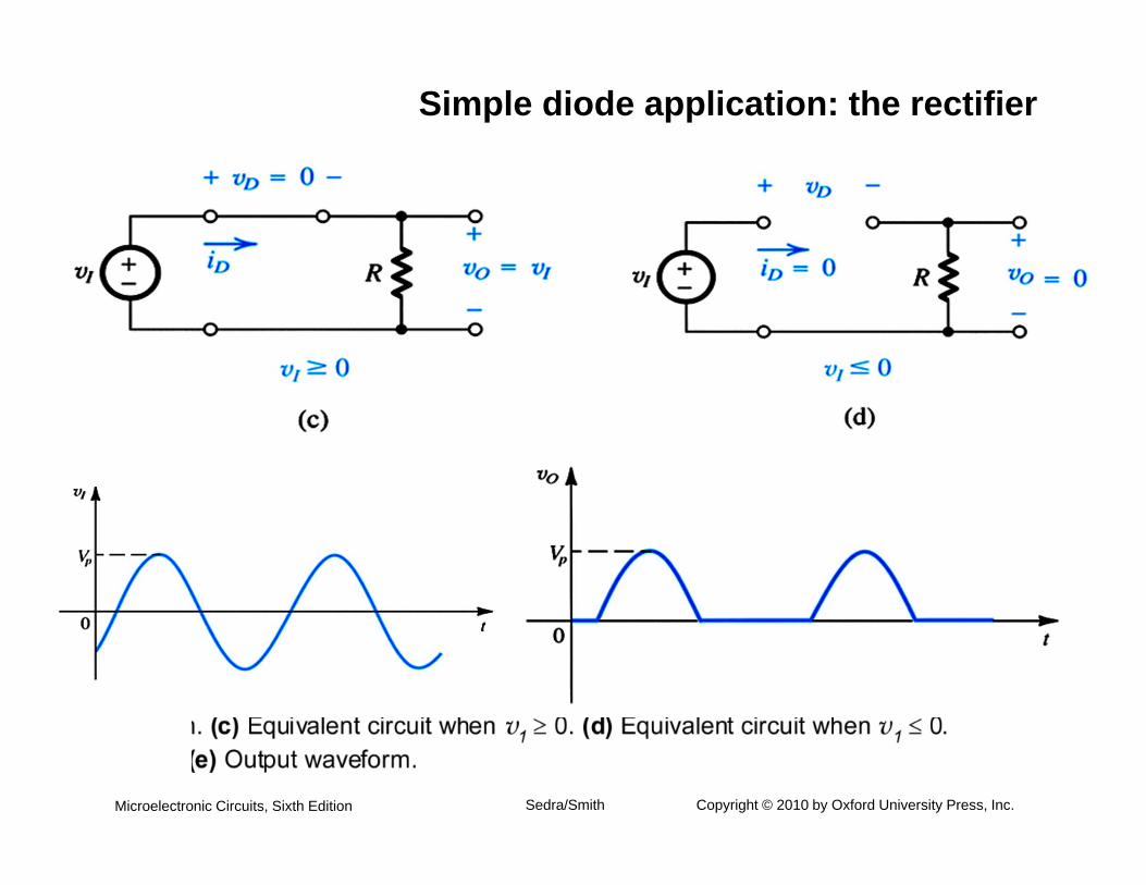
Simple diode application: the rectifier
Microelectronic Circuits, Sixth Edition Sedra/Smith Copyright © 2010 by Oxford University Press, Inc.
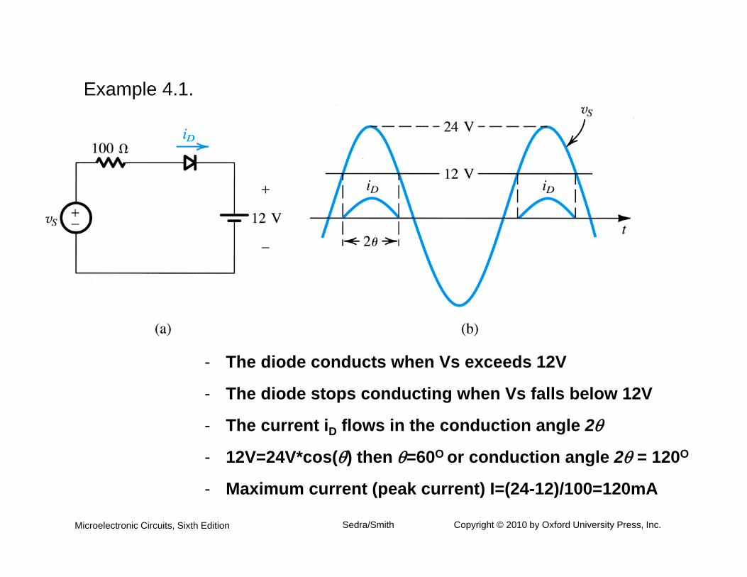
Example 4.1.
- The diode conducts when Vs exceeds 12V
- The diode stops conducting when Vs falls below 12V
- The current iD flows in the conduction angle 2
- 12V=24V*cos() then =60O or conduction angle 2 = 120O
- Maximum current (peak current) I=(24-12)/100=120mA
Microelectronic Circuits, Sixth Edition Sedra/Smith Copyright © 2010 by Oxford University Press, Inc.
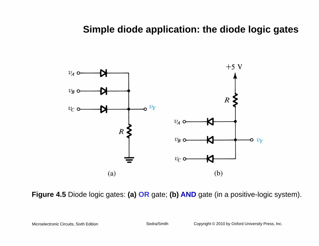
Figure 4.5 Diode logic gates: (a) OR gate; (b) AND gate (in a positive-logic system).
Simple diode application: the diode logic gates
Microelectronic Circuits, Sixth Edition Sedra/Smith Copyright © 2010 by Oxford University Press, Inc.
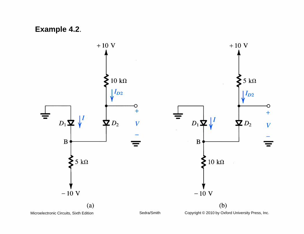
Example 4.2.
Microelectronic Circuits, Sixth Edition Sedra/Smith Copyright © 2010 by Oxford University Press, Inc.
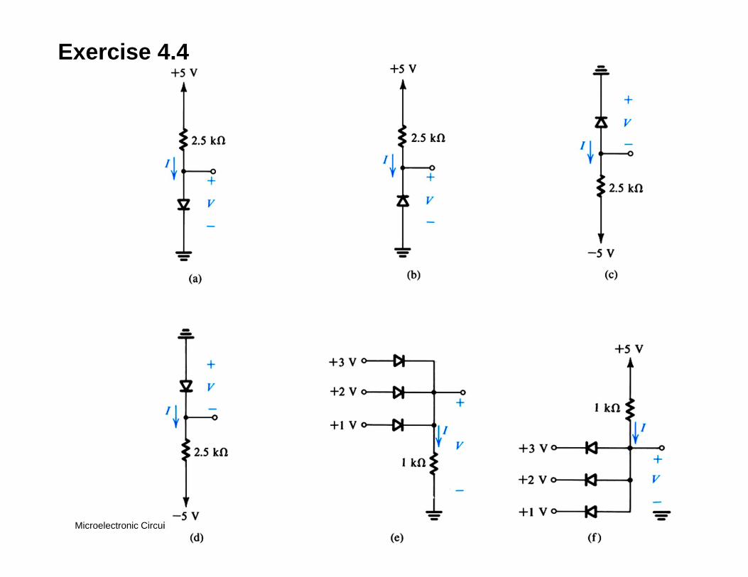
Figure E4.4
Exercise 4.4
Microelectronic Circuits, Sixth Edition Sedra/Smith Copyright © 2010 by Oxford University Press, Inc.
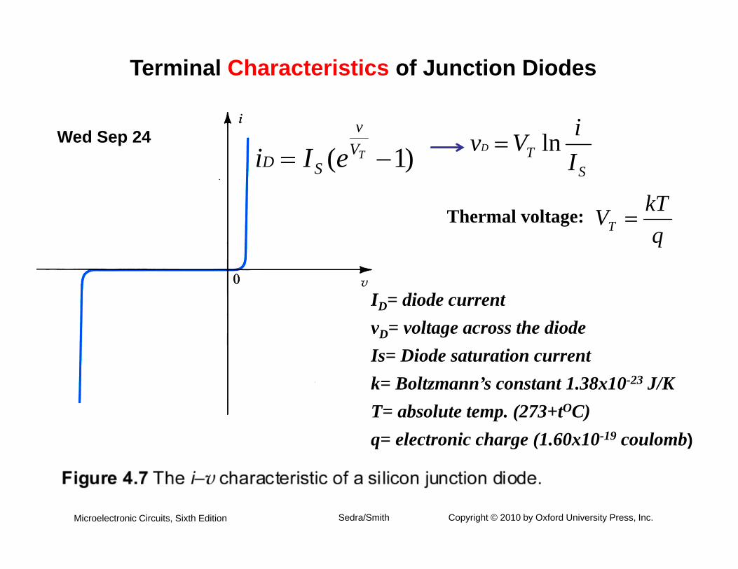
Terminal Characteristics of Junction Diodes
)1( TVv
SD eIi
qkTVT
ST I
iVvD ln
Thermal voltage:
ID= diode currentvD= voltage across the diodeIs= Diode saturation currentk= Boltzmann’s constant 1.38x10⁻²³ J/KT= absolute temp. (273+tOC)q= electronic charge (1.60x10⁻¹⁹ coulomb)
Wed Sep 24
Microelectronic Circuits, Sixth Edition Sedra/Smith Copyright © 2010 by Oxford University Press, Inc.
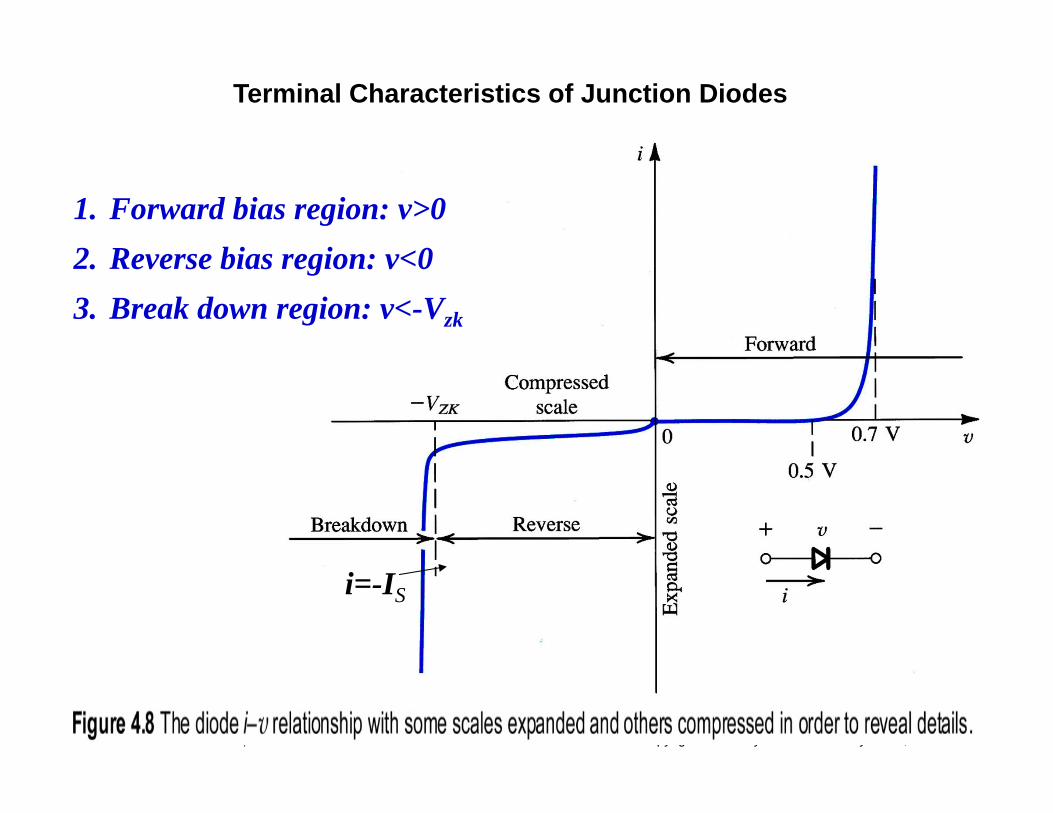
Terminal Characteristics of Junction Diodes
1. Forward bias region: v>02. Reverse bias region: v<03. Break down region: v<-Vzk
i=-IS
Microelectronic Circuits, Sixth Edition Sedra/Smith Copyright © 2010 by Oxford University Press, Inc.
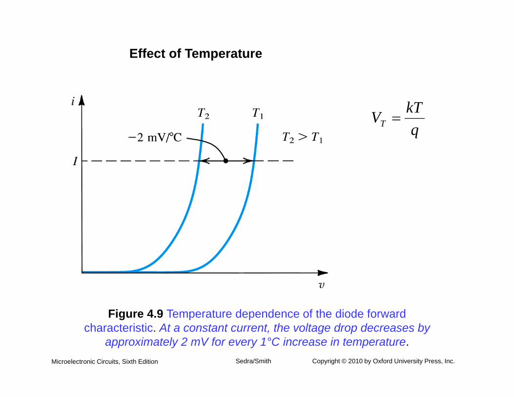
Figure 4.9 Temperature dependence of the diode forward characteristic. At a constant current, the voltage drop decreases by
approximately 2 mV for every 1°C increase in temperature.
qkTVT
Effect of Temperature
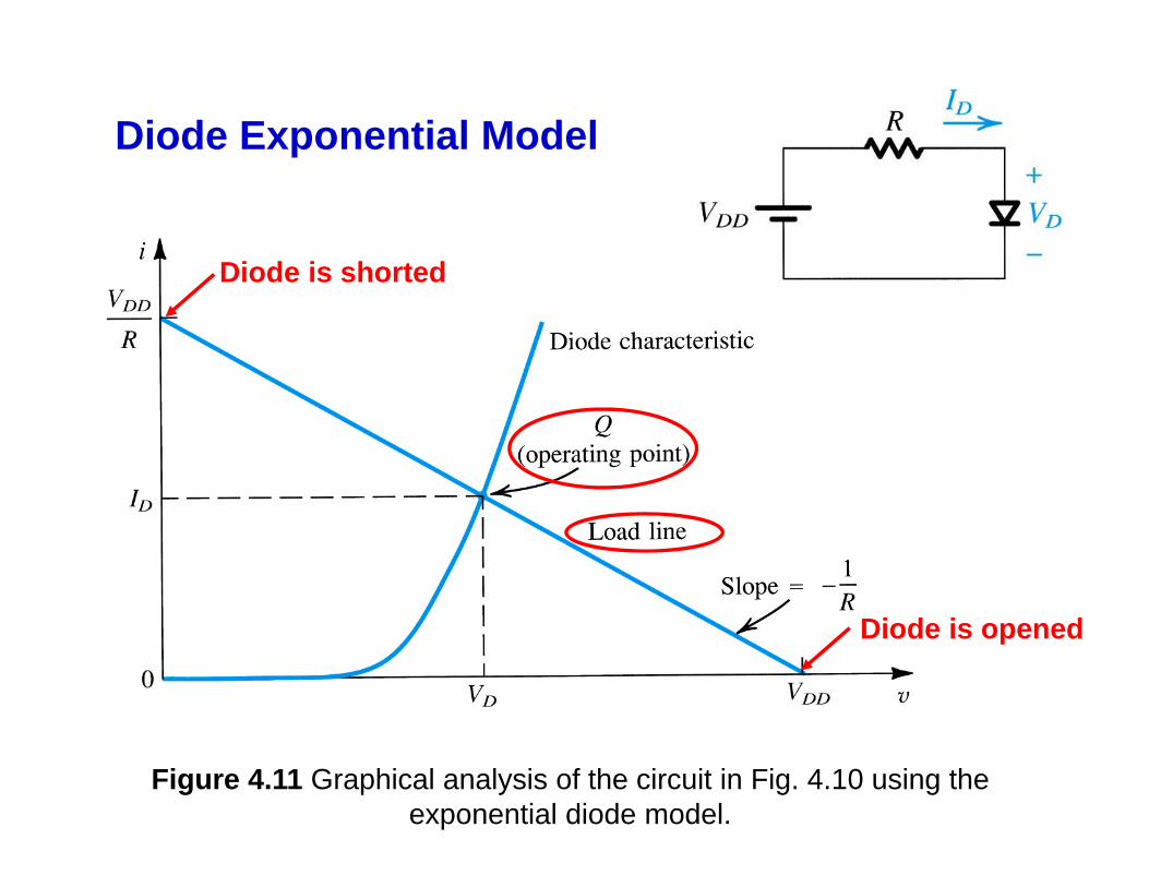
Microelectronic Circuits, Sixth Edition Sedra/Smith Copyright © 2010 by Oxford University Press, Inc.Figure 4.11 Graphical analysis of the circuit in Fig. 4.10 using the
exponential diode model.
Diode Exponential Model
Diode is shorted
Diode is opened
Microelectronic Circuits, Sixth Edition Sedra/Smith Copyright © 2010 by Oxford University Press, Inc.
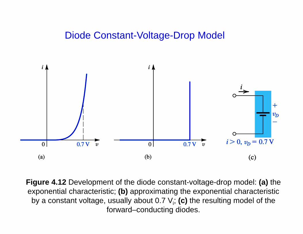
Figure 4.12 Development of the diode constant-voltage-drop model: (a) the exponential characteristic; (b) approximating the exponential characteristic by a constant voltage, usually about 0.7 Vi; (c) the resulting model of the
forward–conducting diodes.
Diode Constant-Voltage-Drop Model
Microelectronic Circuits, Sixth Edition Sedra/Smith Copyright © 2010 by Oxford University Press, Inc.
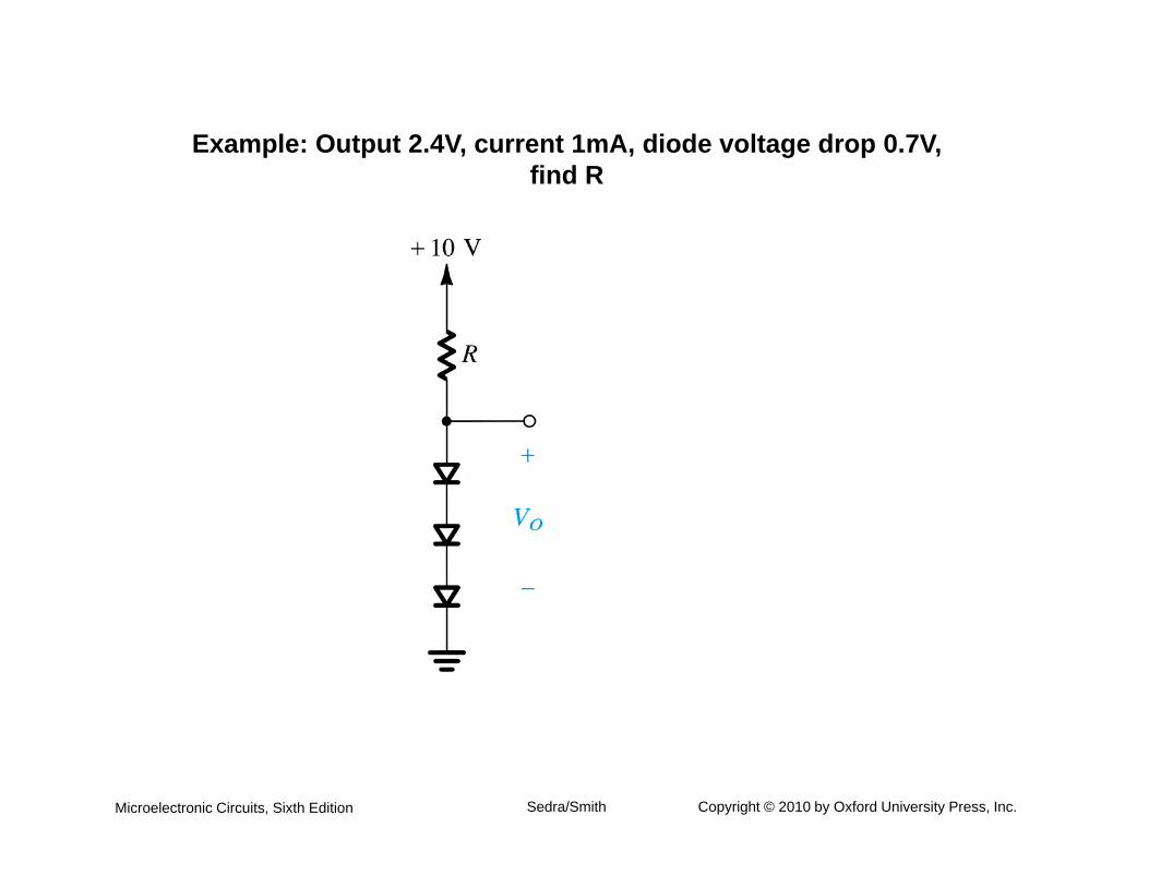
Example: Output 2.4V, current 1mA, diode voltage drop 0.7V, find R
Microelectronic Circuits, Sixth Edition Sedra/Smith Copyright © 2010 by Oxford University Press, Inc.
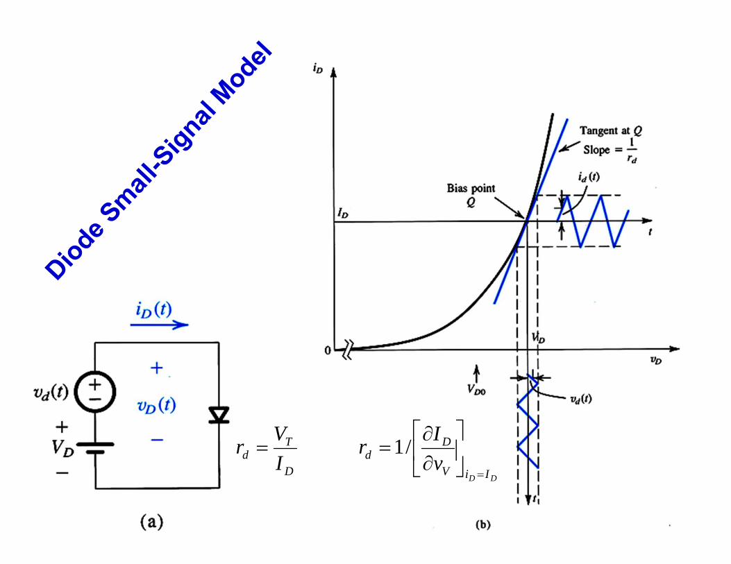
Figure 4.13 Development of the diode small-signal model.DD IiV
Dd
D
Td v
IrIVr
/1
Microelectronic Circuits, Sixth Edition Sedra/Smith Copyright © 2010 by Oxford University Press, Inc.
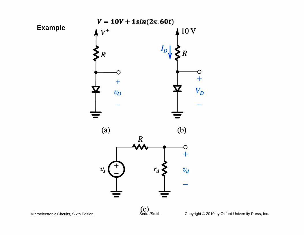
Example
Microelectronic Circuits, Sixth Edition Sedra/Smith Copyright © 2010 by Oxford University Press, Inc.
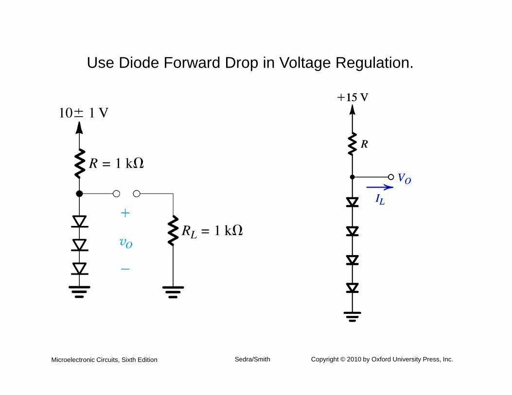
Use Diode Forward Drop in Voltage Regulation.
Microelectronic Circuits, Sixth Edition Sedra/Smith Copyright © 2010 by Oxford University Press, Inc.
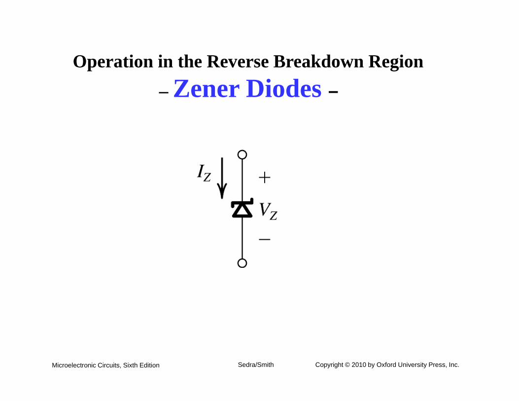
Operation in the Reverse Breakdown Region – Zener Diodes –
Microelectronic Circuits, Sixth Edition Sedra/Smith Copyright © 2010 by Oxford University Press, Inc.
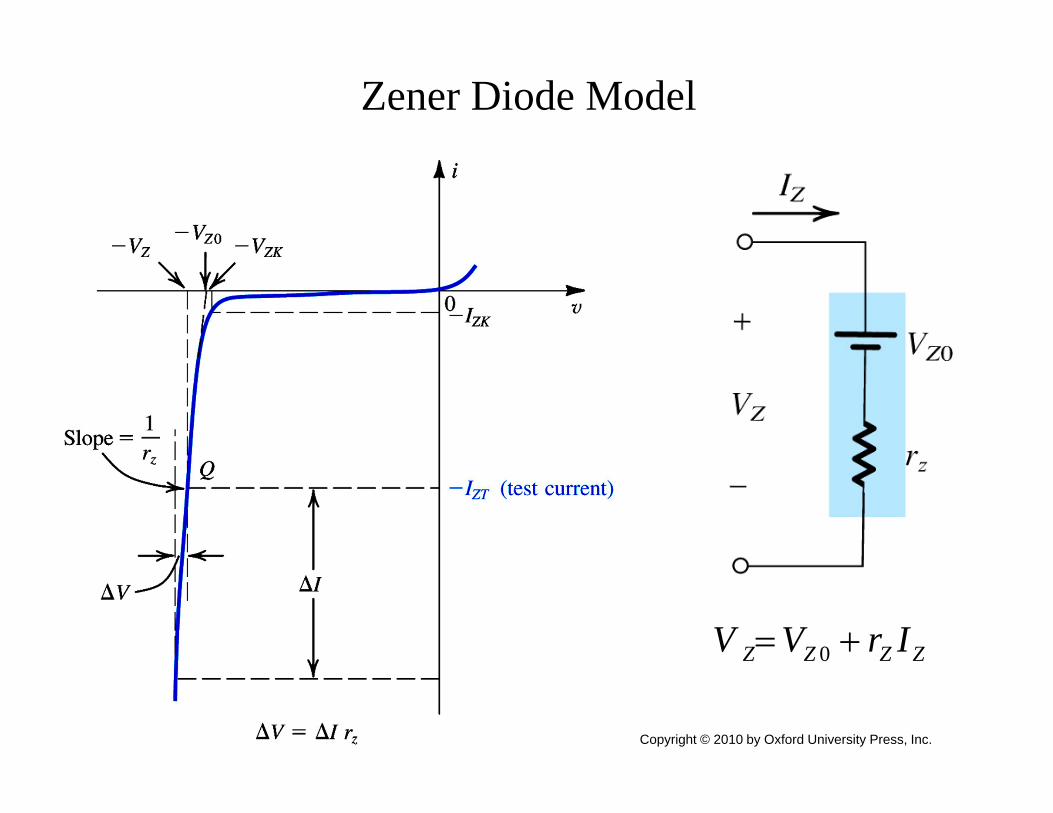
Zener Diode Model
ZZZZ IrVV 0
Microelectronic Circuits, Sixth Edition Sedra/Smith Copyright © 2010 by Oxford University Press, Inc.
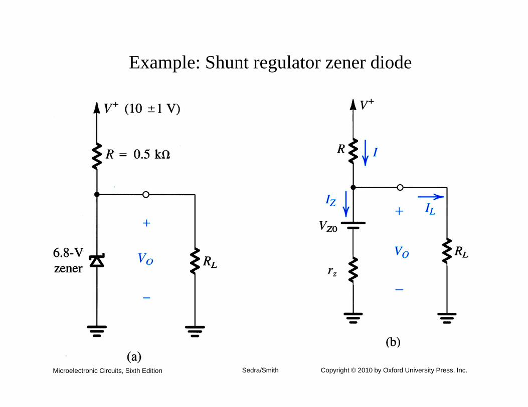
Example: Shunt regulator zener diode
Microelectronic Circuits, Sixth Edition Sedra/Smith Copyright © 2010 by Oxford University Press, Inc.
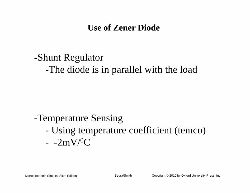
Use of Zener Diode
-Shunt Regulator-The diode is in parallel with the load
-Temperature Sensing- Using temperature coefficient (temco)- -2mV/0C
Microelectronic Circuits, Sixth Edition Sedra/Smith Copyright © 2010 by Oxford University Press, Inc.
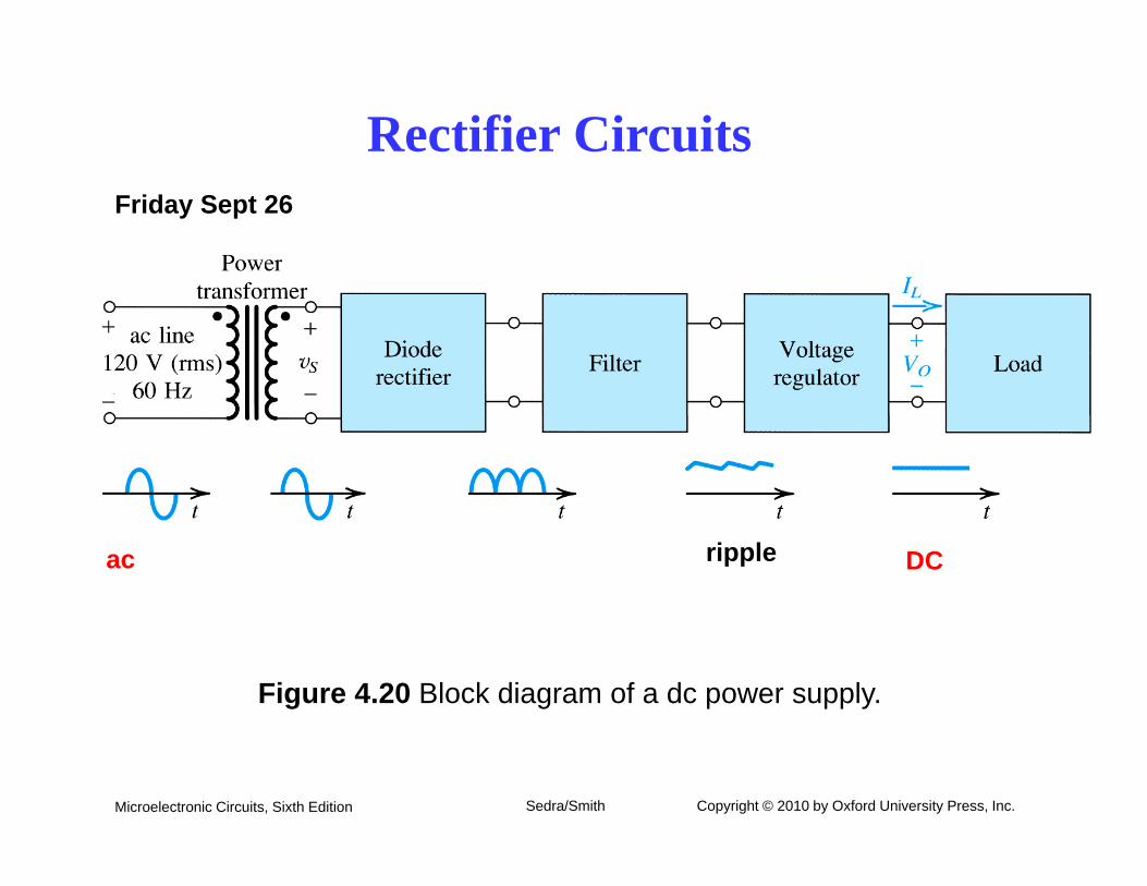
Figure 4.20 Block diagram of a dc power supply.
Rectifier Circuits
rippleac DC
Friday Sept 26
Microelectronic Circuits, Sixth Edition Sedra/Smith Copyright © 2010 by Oxford University Press, Inc.
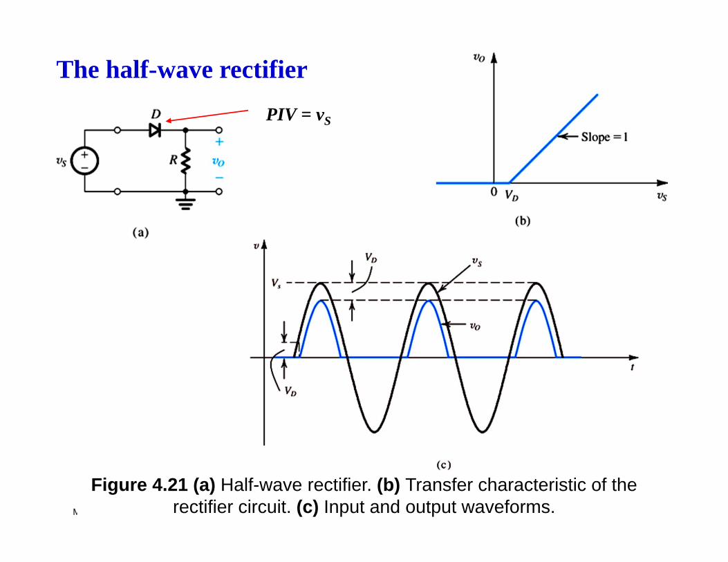
Figure 4.21 (a) Half-wave rectifier. (b) Transfer characteristic of the rectifier circuit. (c) Input and output waveforms.
The half-wave rectifier
PIV = vS
Microelectronic Circuits, Sixth Edition Sedra/Smith Copyright © 2010 by Oxford University Press, Inc.
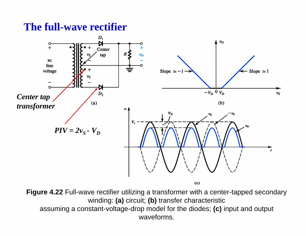
Figure 4.22 Full-wave rectifier utilizing a transformer with a center-tapped secondary winding: (a) circuit; (b) transfer characteristic
assuming a constant-voltage-drop model for the diodes; (c) input and output waveforms.
The full-wave rectifier
PIV = 2vS - VD
Center tap transformer
Microelectronic Circuits, Sixth Edition Sedra/Smith Copyright © 2010 by Oxford University Press, Inc.
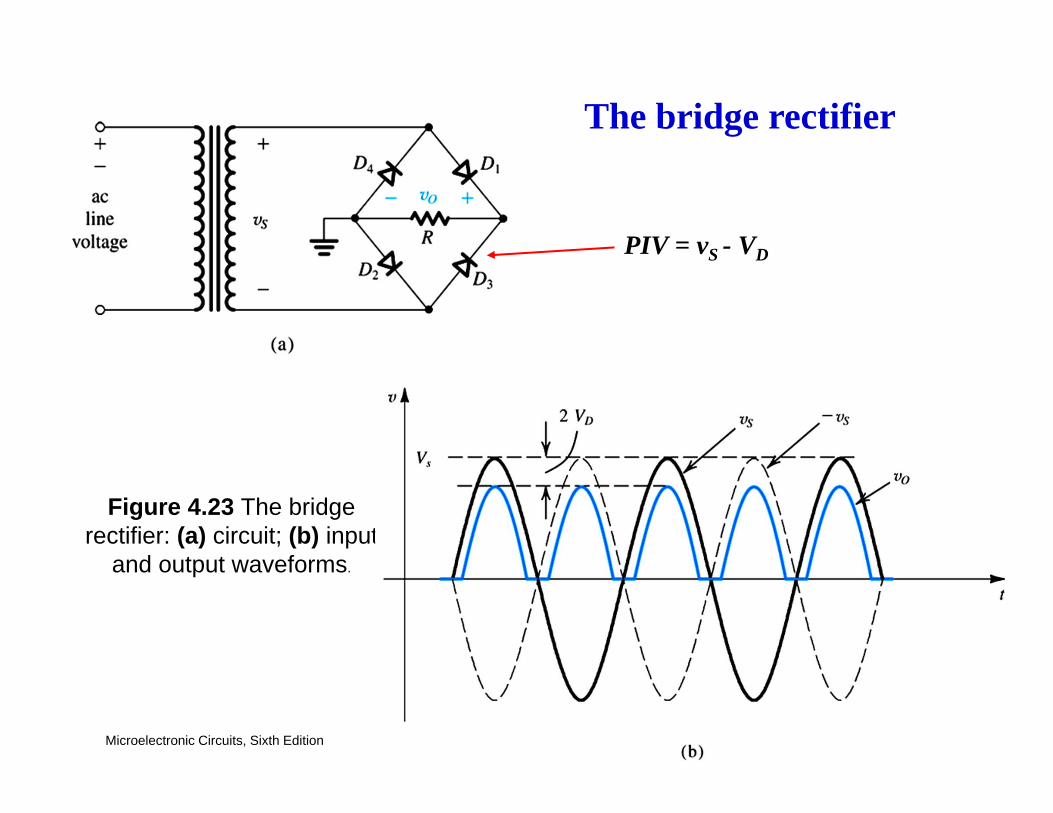
Figure 4.23 The bridge rectifier: (a) circuit; (b) input
and output waveforms.
The bridge rectifier
PIV = vS - VD
Microelectronic Circuits, Sixth Edition Sedra/Smith Copyright © 2010 by Oxford University Press, Inc.
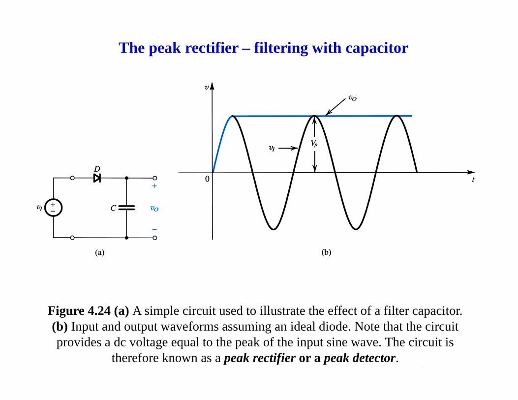
Figure 4.24 (a) A simple circuit used to illustrate the effect of a filter capacitor. (b) Input and output waveforms assuming an ideal diode. Note that the circuit provides a dc voltage equal to the peak of the input sine wave. The circuit is
therefore known as a peak rectifier or a peak detector.
The peak rectifier – filtering with capacitor
Microelectronic Circuits, Sixth Edition Sedra/Smith Copyright © 2010 by Oxford University Press, Inc.
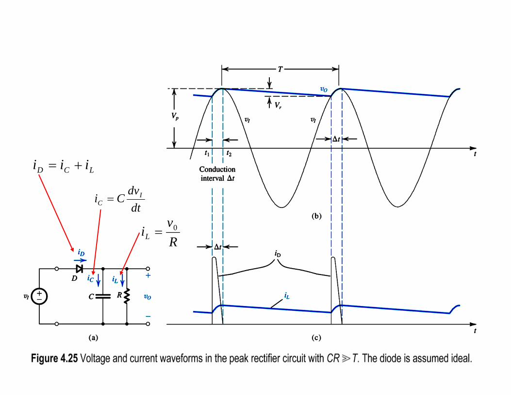
LCD iii
Rv
iL0
dtdv
Ci IC
Microelectronic Circuits, Sixth Edition Sedra/Smith Copyright © 2010 by Oxford University Press, Inc.
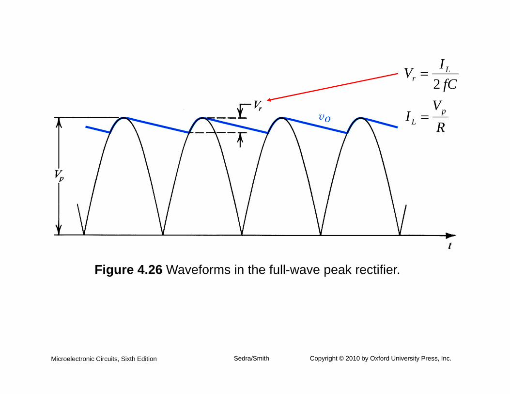
Figure 4.26 Waveforms in the full-wave peak rectifier.
RV
I
fCIV
pL
Lr
2
Microelectronic Circuits, Sixth Edition Sedra/Smith Copyright © 2010 by Oxford University Press, Inc.
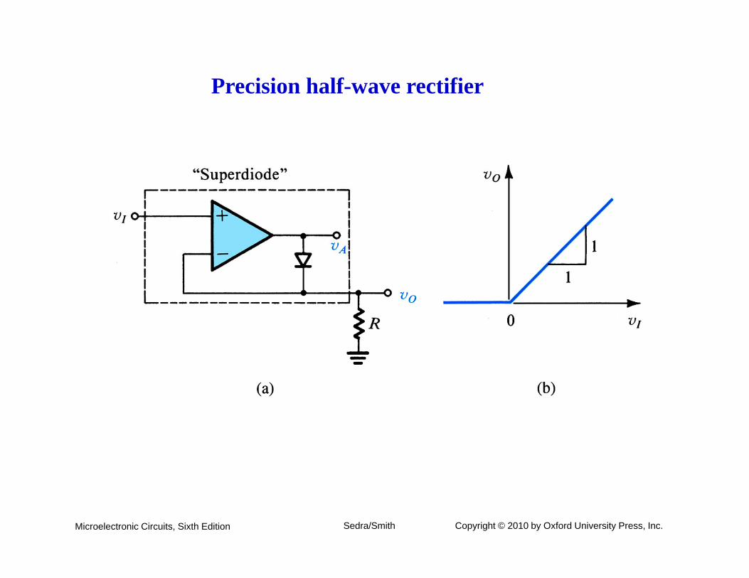
Precision half-wave rectifier
Microelectronic Circuits, Sixth Edition Sedra/Smith Copyright © 2010 by Oxford University Press, Inc.
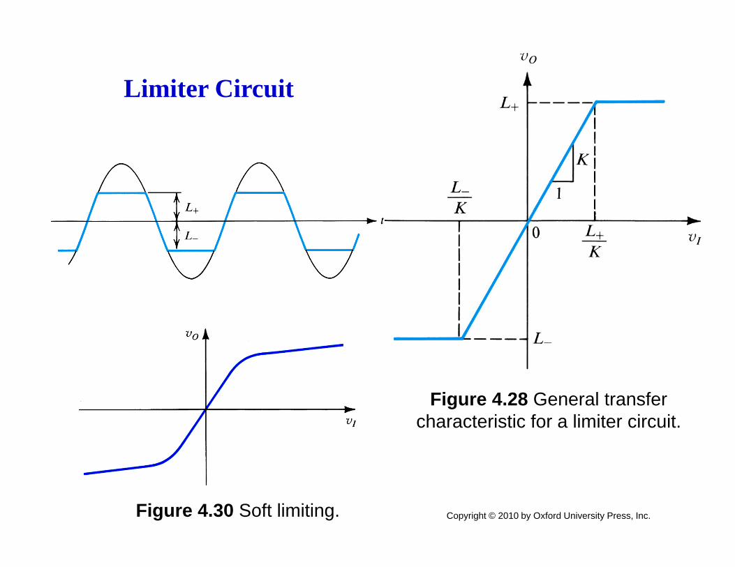
Figure 4.28 General transfer characteristic for a limiter circuit.
Limiter Circuit
Figure 4.30 Soft limiting.
Microelectronic Circuits, Sixth Edition Sedra/Smith Copyright © 2010 by Oxford University Press, Inc.
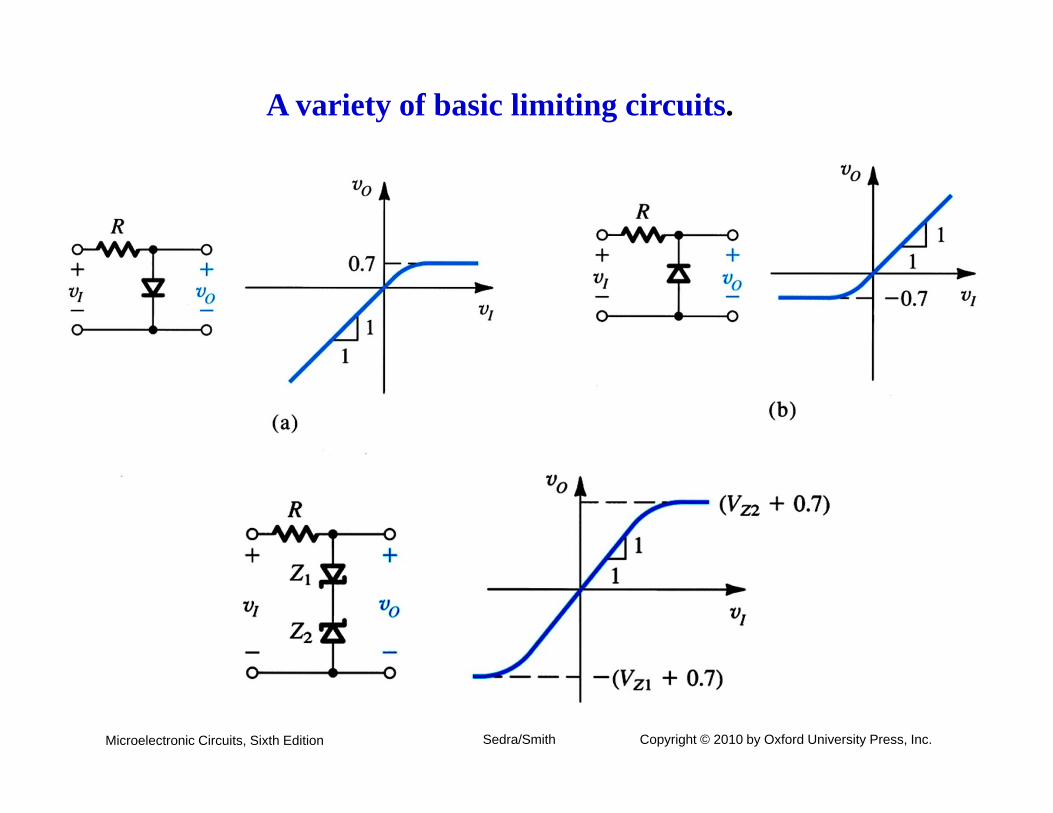
A variety of basic limiting circuits.
Microelectronic Circuits, Sixth Edition Sedra/Smith Copyright © 2010 by Oxford University Press, Inc.
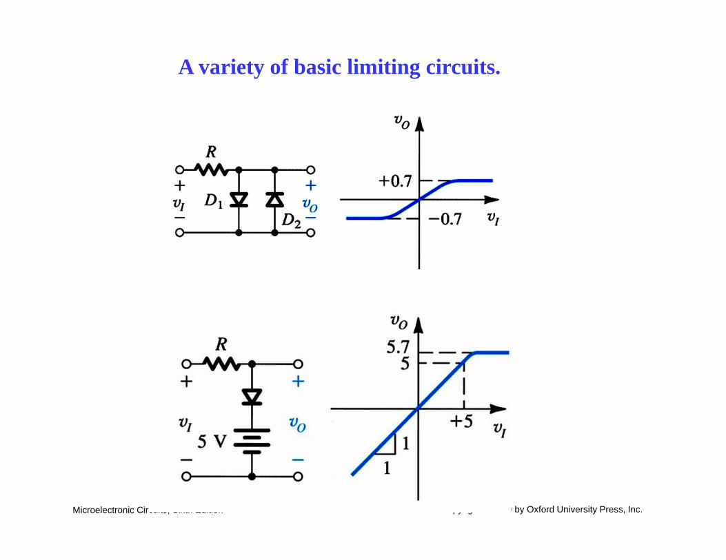
A variety of basic limiting circuits.
Microelectronic Circuits, Sixth Edition Sedra/Smith Copyright © 2010 by Oxford University Press, Inc.
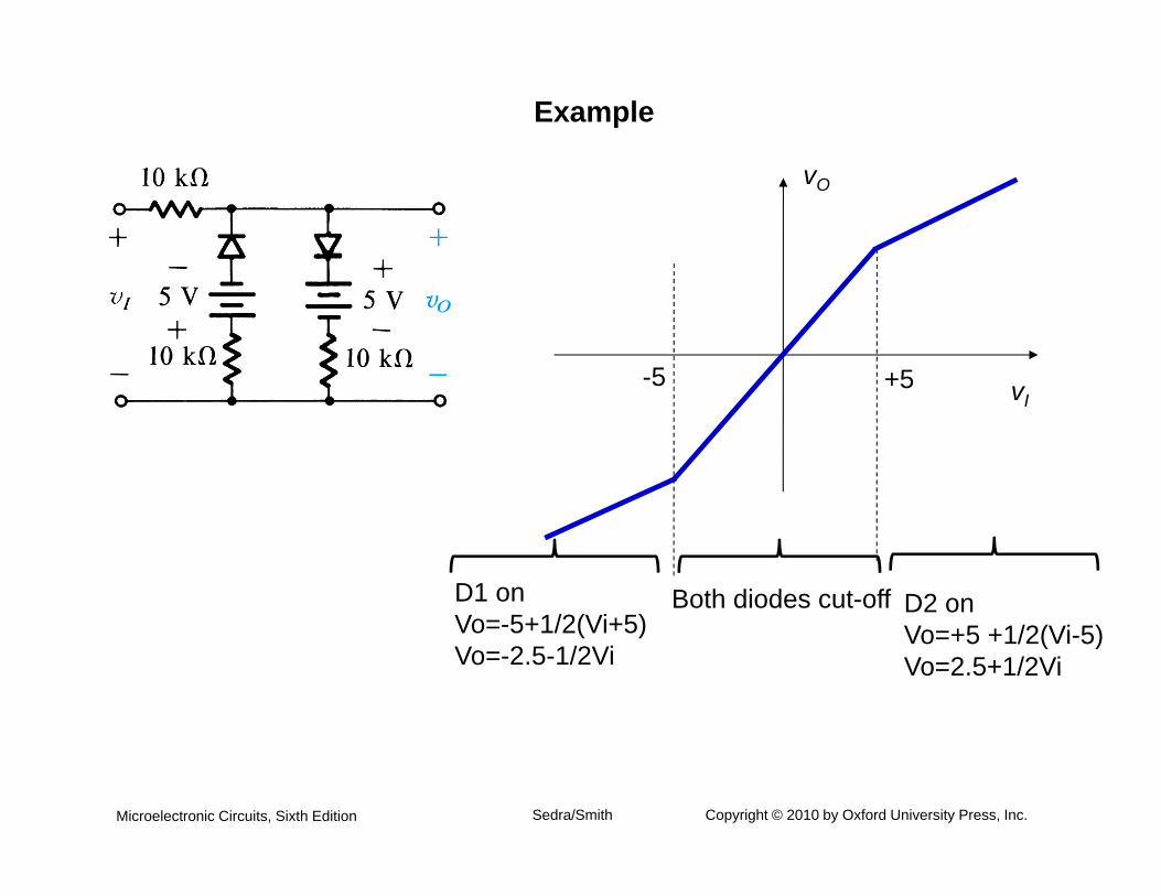
Example
Both diodes cut-off
+5-5 vI
vO
D2 onVo=+5 +1/2(Vi-5)Vo=2.5+1/2Vi
D1 onVo=-5+1/2(Vi+5)Vo=-2.5-1/2Vi
Microelectronic Circuits, Sixth Edition Sedra/Smith Copyright © 2010 by Oxford University Press, Inc.
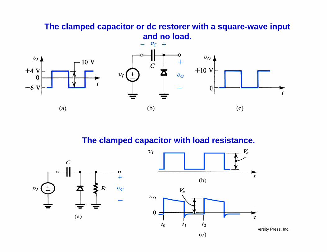
The clamped capacitor or dc restorer with a square-wave input and no load.
The clamped capacitor with load resistance.
Microelectronic Circuits, Sixth Edition Sedra/Smith Copyright © 2010 by Oxford University Press, Inc.
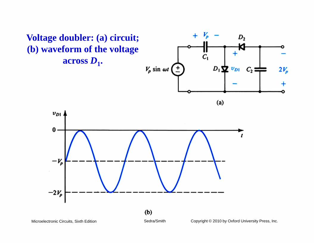
Voltage doubler: (a) circuit; (b) waveform of the voltage
across D1.
Microelectronic Circuits, Sixth Edition Sedra/Smith Copyright © 2010 by Oxford University Press, Inc.
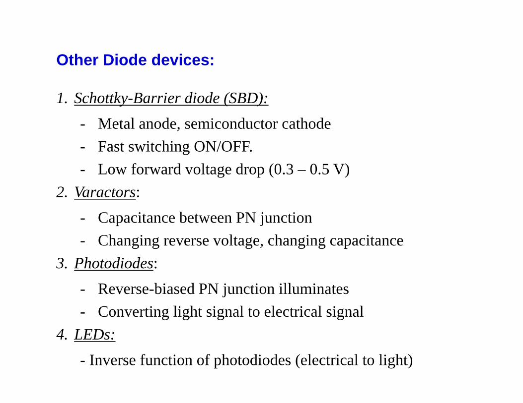
Other Diode devices:
1. Schottky-Barrier diode (SBD):- Metal anode, semiconductor cathode- Fast switching ON/OFF.- Low forward voltage drop (0.3 – 0.5 V)
2. Varactors:- Capacitance between PN junction- Changing reverse voltage, changing capacitance
3. Photodiodes:- Reverse-biased PN junction illuminates- Converting light signal to electrical signal
4. LEDs:- Inverse function of photodiodes (electrical to light)
Microelectronic Circuits, Sixth Edition Sedra/Smith Copyright © 2010 by Oxford University Press, Inc.
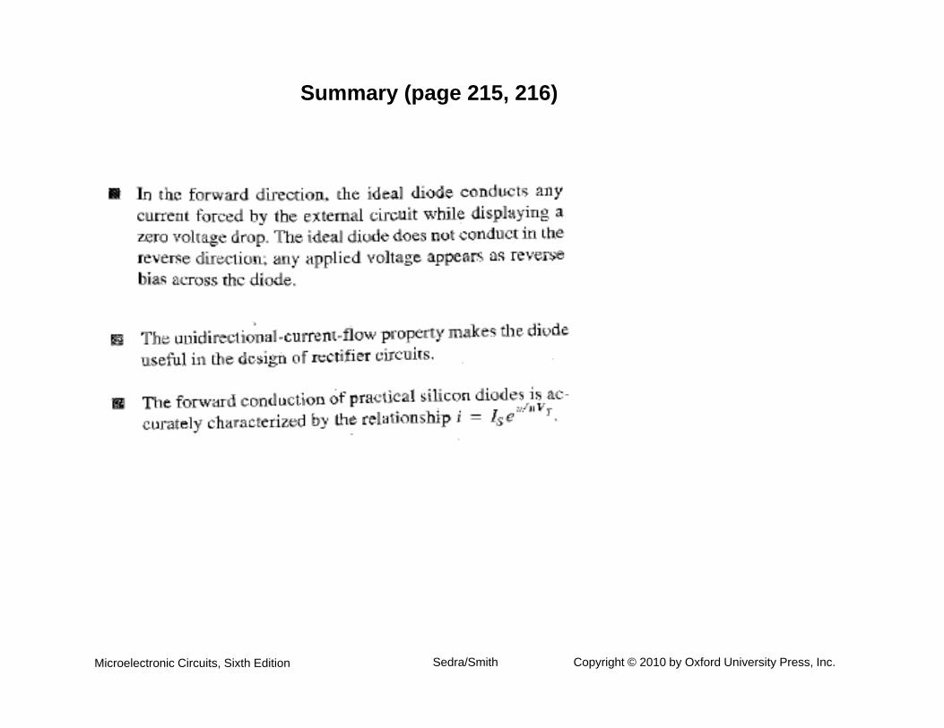
Summary (page 215, 216)
9/26/2014Microelectronic Circuits, Sixth Edition Sedra/Smith Copyright © 2010 by Oxford University Press, Inc.
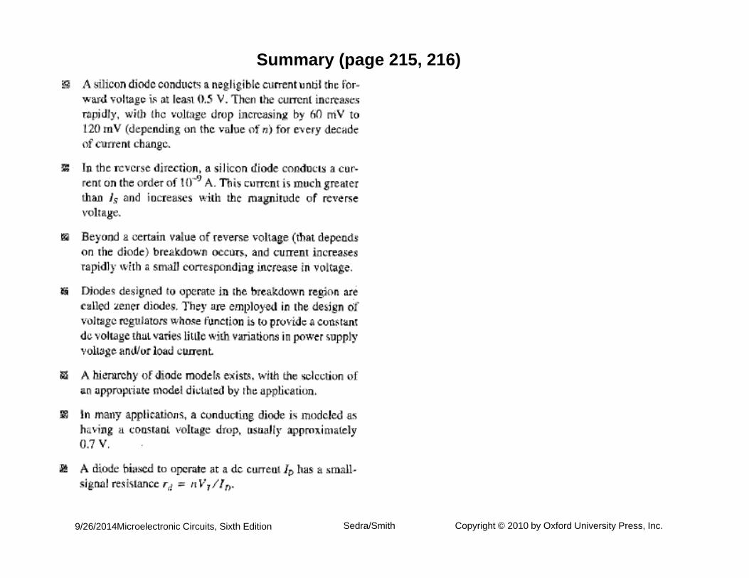
Summary (page 215, 216)


![[ Sedra] Microelectronic Circuits(b Ok.org)](https://static.fdocuments.us/doc/165x107/617b73ef7012c349660bd625/-sedra-microelectronic-circuitsb-okorg.jpg)