Dimension FastScan Pro AFM -...
8
Dimension FastScan Pro AFM Automated Nanometrology and Characterization Atomic Force Microscopy Innovation with Integrity
Transcript of Dimension FastScan Pro AFM -...

Dimension FastScan Pro AFMAutomated Nanometrology and Characterization
Atomic Force MicroscopyInnovation with Integrity

Fast and Cost-Effective Precision Metrology for QA/QC/FAThe Dimension FastScan Pro™ with PeakForce Tapping® delivers
the highest metrology-level speed and performance of any industrial
atomic force microscope (AFM) available today. Designed specifically for
high-volume, production environments, FastScan Pro enables automated or
semi-automated measurements while ensuring the utmost ease of use and
the lowest cost per measurement for quality control, quality assurance,
and failure analysis.
Highest Resolution Imaging and Most, Precise Measurement Performance
PeakForce Tapping enables users to precisely control probe-to-sample interaction, enabling the lowest available imaging forces. This superior force control delivers the most consistent, highest resolution AFM imaging for the widest range of sample types, from soft polymers, thin films and electrical samples to very hard materials.
Unique, Quantitative Results, Whatever You Measure
PeakForce Tapping’s piconewton force sensitivity simultaneously and uniquely combines the highest resolution AFM topography with quantitative, nanoscale electrical and mechanical property mapping, enabling users of all experience levels to achieve precise, accurate measurements.
Easy to Use, Making Every User an AFM Expert
AutoMET™ recipe software and ScanAsyst® ensure unmatched AFM ease of use by eliminating operation complexity. The result is consistently better data and faster metrology results regardless of the operator’s AFM experience level.
Most Reliable Platform and Unrivalled Support
Bruker has the largest service and applications support network of any AFM supplier, with regional customer support and programs for extended support. Major industrial companies and leading data storage and semiconductor manufacturers throughout the world have chosen Bruker systems for their reputation as the most reliable precision metrology platforms.
An alkali-aluminosilicate sheet glass main property is characterized by its strength and scratch resistance, making it challenging to measure its nanometer topography consistently and reliably. Using FastScan AFM and a single Bruker HPI probe, a first image (A) rendered roughness Rq=0.99 nm, Ra=0.79. Image no. 615 (B) rendered the same roughness; Rq=0.99 nm, Ra=0.79. Insets are digitally zoomed images of scan no. 1 and no. 615 revealing insignificant topographical changes.
A
B
Industry-Leading Bruker AFM Technology for Production
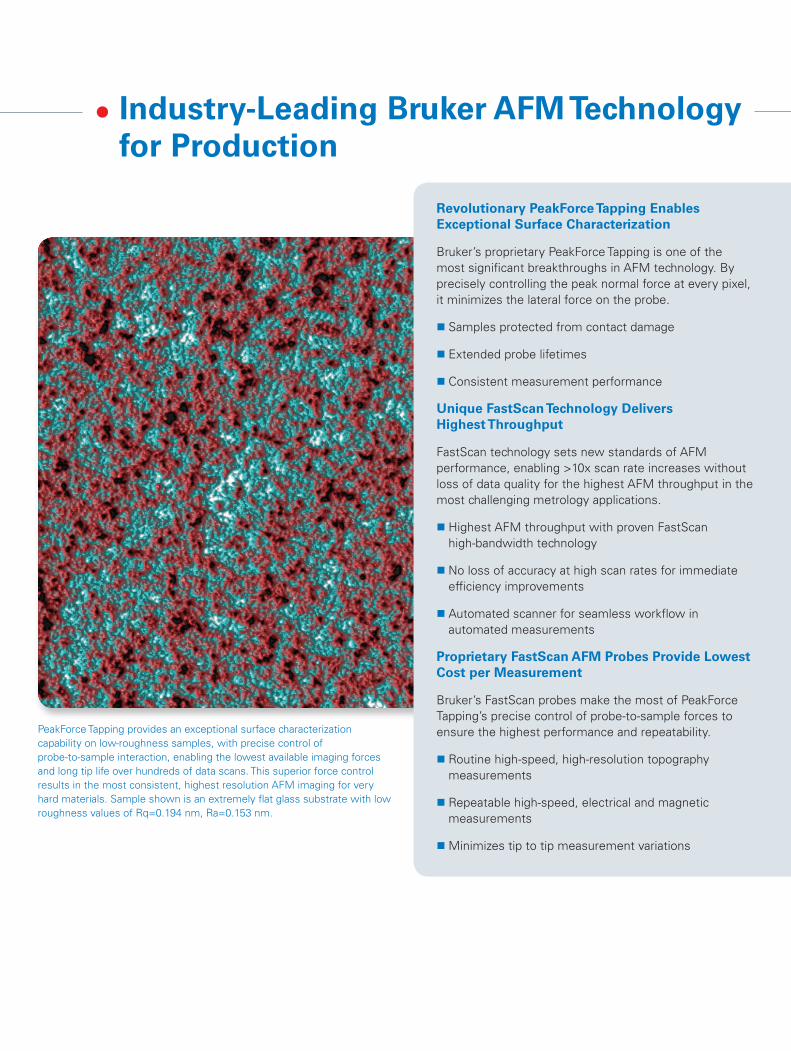
Revolutionary PeakForce Tapping Enables Exceptional Surface Characterization
Bruker’s proprietary PeakForce Tapping is one of the most significant breakthroughs in AFM technology. By precisely controlling the peak normal force at every pixel, it minimizes the lateral force on the probe.
� Samples protected from contact damage
� Extended probe lifetimes
� Consistent measurement performance
Unique FastScan Technology Delivers Highest Throughput
FastScan technology sets new standards of AFM performance, enabling >10x scan rate increases without loss of data quality for the highest AFM throughput in the most challenging metrology applications.
� Highest AFM throughput with proven FastScan high-bandwidth technology
� No loss of accuracy at high scan rates for immediate efficiency improvements
� Automated scanner for seamless workflow in automated measurements
Proprietary FastScan AFM Probes Provide Lowest Cost per Measurement
Bruker’s FastScan probes make the most of PeakForce Tapping’s precise control of probe-to-sample forces to ensure the highest performance and repeatability.
� Routine high-speed, high-resolution topography measurements
� Repeatable high-speed, electrical and magnetic measurements
�Minimizes tip to tip measurement variations
PeakForce Tapping provides an exceptional surface characterization capability on low-roughness samples, with precise control of probe-to-sample interaction, enabling the lowest available imaging forces and long tip life over hundreds of data scans. This superior force control results in the most consistent, highest resolution AFM imaging for very hard materials. Sample shown is an extremely flat glass substrate with low roughness values of Rq=0.194 nm, Ra=0.153 nm.
A Proven AFM Performance LeaderThe Dimension platform has the largest installed base of any AFM in the semiconductor, data storage, high-brightness LED and polymer industries. Its open-access platform, large– or multiple-sample holders, and numerous ease-of-use features open up the power of atomic force microscopy to manufacturers, delivering the best solution for nanoscale metrology in QA/QC/FA—cost effectively and reliably.
� Automated, highest accuracy metrology
� Automated 2-inch to 12-inch wafer measurements for semi, data storage and HB-LED
� Reliable platform designed for use in industrial environments
NanoScope Provides Fast, Intuitive Sample Navigation
The FastScan Pro’s NanoScope® navigation interface provides fast and intuitive sample navigation to quickly and easily find your area of interest. Pan and zoom features for fast setup and scan speeds up to 100 times the standard AFM scan rates significantly reduce measurement time.
� Easy step-by-step navigation makes measurement sessions simple
� Pan and zoom efficiently locate the region of interest
� Preconfigured software settings easily integrate the system into manufacturing workflow
ScanAsyst Eliminates the Complexity of AFM Operation
ScanAsyst is a PeakForce Tapping-based image-optimization mode that enables users of all experience levels to obtain the highest measurement performance. The user simply selects a sample scan area and scan size, and ScanAsyst takes over, creating a turnkey solution for AFM imaging. ScanAsyst eliminates the need to navigate complicated AFM interfaces and parameter settings. Intelligent algorithms automatically and continuously monitor the image quality and make needed parameter adjustments.

Automation Software Ensures Exceptional Ease of Use
New AutoMET full-recipe software delivers fast, automated metrology, simple operation, and AFM adaptability for easy capture of critical-to-quality measurements needed in production.
� Automated measurements on multiple samples or a single large sample for nanoscale characterization across multiple locations
� Optical and AFM image pattern recognition, tip-centering, full wafer or grid mapping support, and image-placement accuracy within tens of nanometers
� Comprehensive yet simple recipe writing for the advanced user or engineer available for real-time and offline use
� Easy setup to align sample to probe and alignment corrections to AFM environment
Data Analysis Flexibility for Varied Measurement Needs
NanoScope Analysis is a robust software package that supports remote data analysis of images via linked communication to FastScan Pro. This greatly expands the capability for analysis of data, either in real-time on the FastScan Pro or offline at your desk.
Top: Recipe window showing grid-based layout for user-defined measurement locations on rectangular or square scan areas. Lower: Recipe window showing wafer-based layout for precise, user-defined X-Y measurement locations within a wafer.
Easy measurement recipe creation, allows engineers to define location by name, assign any type, and number measurements at each location.
Specifically Designed for Measurements in a Production Environment
Highest Accuracy Roughness, Depth and Height Measurements
Dimension FastScan Pro provides highly repeatable and accurate roughness, height and depth measurements, from sub-nanometer steps to high-aspect ratio trenches using PeakForce Tapping or TappingMode.
Most Comprehensive Defect Review Characterization
Nanoscale defects can be located and characterized on a variety of wafers, substrates and sliders. PeakForce QNM can uniquely provide combined 3D imaging and mechanical property information.
Widest Range of Measurement Types
From our newest PeakForce Tapping modes to traditional AFM modes, FastScan Pro provides the greatest range and flexibility to meet your specific measurement and characterization needs on a wide range of samples.
Unique Fast Nano-Electrical Measurements
FastScan technology with Conductive-AFM (CAFM) can perform nanoscale current measurements at high scan rates, significantly increasing the efficiency of failure analysis measurement. Using a small magnetic force microscopy (MFM) cantilever, FastScan Pro provides greater than 10x scan rate improvements for MFM applications with exceptional data quality using PeakForce Tapping. PeakForce KPFM™ provides the highest spatial resolution and most accurate measurements of surface potential. PeakForce TUNA™ provides the most sensitive conductivity measurements.
Precise Nanoscale Mechanical Mapping
Bruker’s unique PeakForce QNM® and FastForce Volume™ nanoscale mechanical mapping modes can precisely map mechanical properties—modulus, stiffness, adhesion, dissipation, and deformation—while simultaneously imaging sample topography and electrical properties. PeakForce QNM enables non-destructive measurements on polymers, thin films, and nanoscale defects not measurable by transmission electron or scanning electron microcopy techniques.
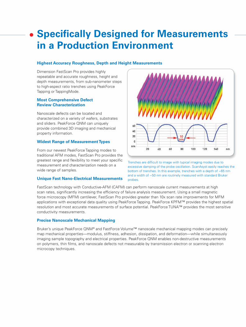
Trenches are difficult to image with typical imaging modes due to excessive damping of the probe oscillation. ScanAsyst easily reaches the bottom of trenches. In this example, trenches with a depth of ~65 nm and a width of ~50 nm are routinely measured with standard Bruker probes.

Semiconductor
� Bare wafer roughness metrology and defect review characterization
� Nanometer-node electrical device characterization and fault isolation
� Accurate step height and depth metrology measurements
Data Storage
�Most precise, highest resolution and high high-throughput, production-based slider metrology
�Media substrate roughness and defect review characterization with outstanding resolution
� Electrical and magnetic failure analysis characterization for wafer, media, and slider
Polymers and Thin Films
� high-throughput, topography measurements for quality control
� Simultaneous topography and mechanical property mapping
� Suitable for a wide range of block co-polymers
High-Brightness LED and Solar Materials
� Automated HB-LED pattern sapphire (PSS) depth and shape metrology
� Precise HB-LED substrate roughness
� Electrical characterization of HB-LED and solar materials
MEMS Manufacturing
� Automated measurement of roughness, height, and shape
�Mechanical property characterization (displacement, strain) of actuators
� Electrical characterization of MEMS devices
Semi-automated 24/7 operations using a Dimension AFM to characterize 3D geometry for process control.
Bruker’s AFMs and high-performance industrial probes provide consistent and reliable measurements for the most demanding critical-to-quality nanoscale measurements.
Unlimited Applications
0 50 100 150 200 250 300 350 400 450
0.050
0
0.100
0.150
0.200
0.250
Image Rq (nm)
Modulus map of a multi-component polymer blend imaged using PeakForce QNM. There are three different components clearly present, the light blue component (A), the darker blue component (B), and the red/black component (C). (7 µm scan).

Bruker Nano Surfaces Division
Santa Barbara, CA • USA Phone +1.805.967.1400/800.873.9750 [email protected]
www.bruker.com/fastscanpro
© 2016 Bruker Corporation. All rights reserved. AutoMET, Dimension FastScan Pro, Dimension Icon, PeakForce KPFM, PeakForce QNM, PeakForce Tapping, PeakForce TUNA, ScanAsyst, and TappingMode are trademarks of Bruker Corporation. All other trademarks are the property of their respective companies. Bruker Nano Surfaces Division is continually improving its products and reserves the right to change specifications without notice. B083, Rev. A1.
Icon Scan Head FastScan Scan Head
X-Y scan range 90 µm x 90 µm typical, 85 µm minimum
35 µm x 35 µm typical, 30 µm minimum
Z range 10 µm typical in imaging and force curve modes, 9.5 µm minimum
≥3 µm
Vertical noise floor*<35 pm RMS, height sensor in appropriate environment, typical imaging BW (up to 625 Hz)
<55 pm RMS, height sensor in appropriate environment (up to 625 Hz)
X-Y position noise≤0.15 nm RMS typical imaging BW (up to 625 Hz)
≤0.20 nm RMS typical imaging BW (up to 2.5 kHz in adaptive mode)
X-Y flatness (30 µm range) NA ≤3 nm
Integral nonlinearity (X-Y-Z) <0.50%
Scanner laser alignment Manual Automated laser and detector alignment
Sample size/holder 200 mm vacuum chuck for samples ≤200 mm in diameter, ≤15 mm thick
Motorized position stage (X- Y)
Inspectable area; 200 mm × 200 mm, ≤±6 µm repeatability
Bidirectional positional accuracy enabled by automated software recipes; 95%, <±2 µm with optical pattern recognition and <50 nm through tip centering and SPM zoom features
Microscope optics 5MP digital camera; 180 µm to 1465 µm viewing area, digital zoom and motorized focus
5MP digital camera; 130 µm to 1040 µm viewing area, digital zoom and motorized focus
Controller/Software NanoScope V/NanoScope v9.1 and later
AutoMET automation software
AutoMET software including global wafer registration using pattern recognition to compensate wafer deskew and offset; Tip centering to compensate tip offset; Autofocus on tip and sample; Die selector by map graph
Workstation NanoScope V, stage controller, HV amplifiers, computer, ergonomic design with immediate physical and visual access
Vibration and acoustic isolation Integrated (refer to installation requirements for additional information)
EH&S compliance CE certified
* Dependent on facility environmental noise emissions. Consult Bruker specialist to establish a plan for ultimate performance.