Digitally Tunable Band-Pass Filter · QEX January/February 2016 5 side the band of interest. Figure...
6
QEX January/February 2016 3 Rua Cel Manuel de Moraes 204, Campinas, SP 13073-022, Brazil; [email protected] Digitally Tunable Band-Pass Filter Computer control tunes this versatile band-pass filter to meet changing requirements. 1 Notes appear on page 8 Band-pass filters have always been important, but new hardware technology has made them even more significant. In environ- ments with large amounts of electromagnetic pollution, this new type of band-pass filter can be very helpful. To construct the digitally tunable band- pass filter, I used digitally tunable capacitors (DTC). These components have a variable capacitance that can be controlled digitally. The digitally tunable band-pass filter in this article covers a frequency range of 132 MHz to 148 MHz, and can handle up to 26 dBm of RF power. It can be integrated into dif- ferent projects, including software defined radio (SDR) projects, where the band-pass filters are of fundamental importance to the end result. Digitally Tunable Capacitors (DTCs) The key parts of the band-pass filter described in this article are digitally tunable capacitors (DTCs), which are made up of several high-Q-factor metal-insulator-metal (MIM) capacitors, which are digitally con- trolled FET switches. Figure 1 is a functional block diagram of a DTC. The DTC used in the design of this proj- ect is the Peregrine PE64102, which has a capacitance range of 1.88 pF to 14.0 pF in steps of 391 fF, totaling 32 states that are con- trolled with 5 bits through a serial peripheral interface (SPI) bus. 1 The Peregrine PE64102 works at 100 MHz to 3 GHz, and can handle up to 26 dBm of RF power. Design the Filter Basically, a band-pass filter is used to attenuate all signals having frequencies out- Euclides Lourenço Chuma, PY2EAJ The Computer, Arduino Uno and band-pass filter circuit board. QX1601-Chuma01 RF+ Serial Interface CMOS Control Driver and ESD RF– ESD ESD Figure 1 — This is a functional block diagram of the digitally tunable capacitors.
Transcript of Digitally Tunable Band-Pass Filter · QEX January/February 2016 5 side the band of interest. Figure...

QEX January/February 2016 3
Rua Cel Manuel de Moraes 204, Campinas, SP 13073-022, Brazil; [email protected]
Digitally Tunable Band-Pass Filter
Computer control tunes this versatile band-pass filter to meet changing requirements.
1Notes appear on page 8
Band-pass filters have always been important, but new hardware technology has made them even more significant. In environ-ments with large amounts of electromagnetic pollution, this new type of band-pass filter can be very helpful.
To construct the digitally tunable band-pass filter, I used digitally tunable capacitors (DTC). These components have a variable capacitance that can be controlled digitally. The digitally tunable band-pass filter in this article covers a frequency range of 132 MHz to 148 MHz, and can handle up to 26 dBm of RF power. It can be integrated into dif-ferent projects, including software defined radio (SDR) projects, where the band-pass filters are of fundamental importance to the end result.
Digitally Tunable Capacitors (DTCs)The key parts of the band-pass filter
described in this article are digitally tunable capacitors (DTCs), which are made up of several high-Q-factor metal-insulator-metal (MIM) capacitors, which are digitally con-trolled FET switches. Figure 1 is a functional block diagram of a DTC.
The DTC used in the design of this proj-ect is the Peregrine PE64102, which has a capacitance range of 1.88 pF to 14.0 pF in steps of 391 fF, totaling 32 states that are con-trolled with 5 bits through a serial peripheral interface (SPI) bus.1 The Peregrine PE64102 works at 100 MHz to 3 GHz, and can handle up to 26 dBm of RF power.
Design the FilterBasically, a band-pass filter is used to
attenuate all signals having frequencies out-
Euclides Lourenço Chuma, PY2EAJ
The Computer, Arduino Uno and band-pass filter circuit board.
QX1601-Chuma01
RF+
SerialInterface
CMOS ControlDriver and ESD
RF–
ESD ESD
Figure 1 — This is a functional block diagram of the digitally tunable capacitors.
4 QEX January/February 2016
QX1601-Chuma02
–3 dB
Bandwidth
QX1601-Chuma03
X
X(A)
Generator And Load
Rs
RL
VL2
Vs Filter
(B)Generator, Filter And Load
Rs
RL
VL1
Vs
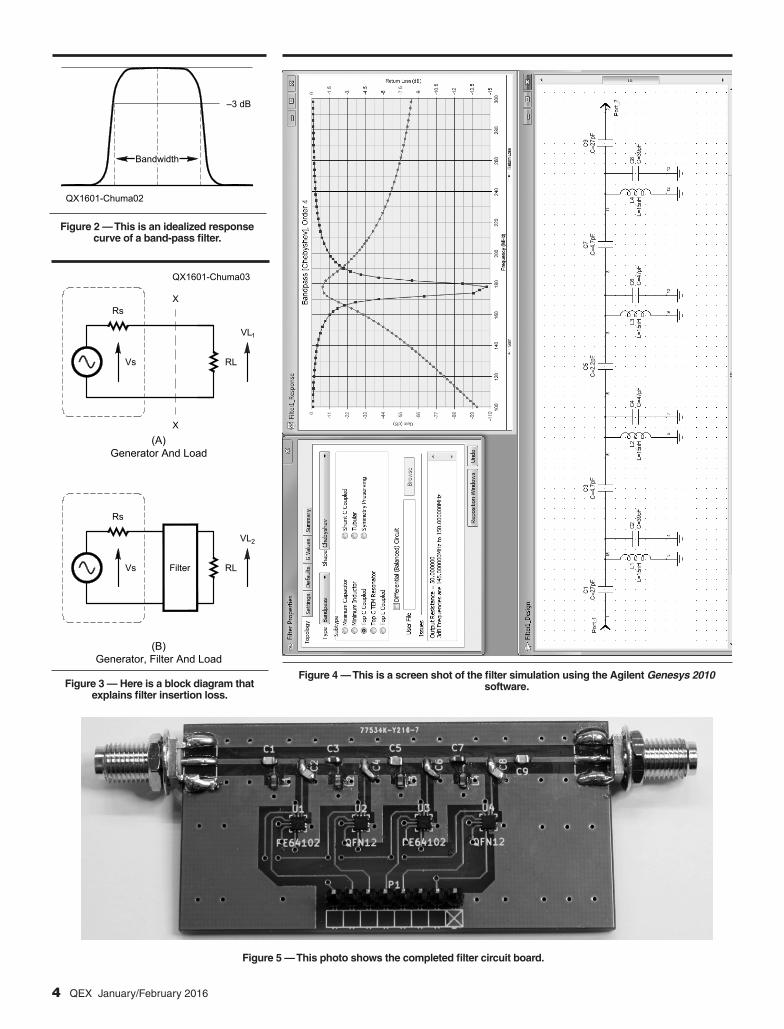
Figure 2 — This is an idealized response curve of a band-pass filter.
Figure 3 — Here is a block diagram that explains filter insertion loss.
Figure 4 — This is a screen shot of the filter simulation using the Agilent Genesys 2010 software.
Figure 5 — This photo shows the completed filter circuit board.

QEX January/February 2016 5
side the band of interest. Figure 2 shows the frequency response of a real band-pass filter, where fc is the center frequency and the band-width is the difference between frequencies f1 and f2, where the attenuation is 3 dB com-pared with the magnitude of fc.
To develop a band-pass filter, we need to know several filter details, such the center frequency, bandwidth, terminating resis-tance, type of filter response (Butterworth, Chebychev, Elliptical, and so on), and fil-ter order. With these parameters, we can design our filter using simulation software or through manual calculations (hard work).
Several criteria are used to measure the performance of a filter, but the ones used most are the insertion loss and return loss. Insertion loss is the loss of signal power resulting from the insertion of a filter in the transmission line. In Figure 3, if RL = Rs then VL1 is half of Vs. If you add a filter between the generator and the load at position X-X, then any additional loss is the result of the insertion loss of the filter.
For the band-pass filter development of this article I used the Genesys 2010 software from Agilent. I chose the band-pass filter “Top C Coupled” and Chebyshev type, of order 4 and with 5 MHz of bandwidth. After the first tests, it became clear that there was a downshift of the frequency range, and so I made some changes in component values to achieve the frequency range of 132 MHz to 148 MHz.
The model “Top C Coupled” filter was chosen to use fewer inductors (where Q is critical), and also to come up with a design that uses component values that are available on the market.
Building ItThe biggest challenge in building the fil-
ter was the size of the digitally tunable capac-itors. They are available as a quad flat-pack, no-lead 12-pin package with dimensions of 2 × 2 mm and 0.5 mm pin spacing!
The circuit board design was done in Kicad software and the manufacture was made with common characteristics (2-Layer FR4 1.6 mm).
The capacitors used are commonly avail-able, with 5% tolerance, but the ideal would be to use pre-selected NP0 capacitors. The inductors are manufactured by Coilcraft, and have a Q of about 40 at 150 MHz. The inductors also offer a certain challenge to be soldered in place on the circuit board. The finished circuit board is shown in Figure 5. Figure 6 is the schematic diagram of the digi-tally tunable band-pass filter.
ControlsI adapted an Arduino Uno circuit board
Figu
re 6
— H
ere
is th
e sc
hem
atic
dia
gram
of t
he d
igita
lly tu
nabl
e ba
nd-p
ass
filte
r.
QX
1601
-Chu
ma0
6
RF+
10
RF+
SD
AT
129G
ND
SE
N1
11
GN
D
SC
LK3
8
RF–
7
RF–
6
GN
D5
GN
D2
PE
6410
2-Q
FN12
U4
8
CO
NN
_01X
08
P1
7 6 5 4 3 2 1
J1 SM
AJ2 SM
AC
127
pF
L115
nH
C2
39 p
F
C3
4.7
pF
L215
nH
C4
47 p
F
C5
1.5
pF
L315
nH
C6
47 p
F
C7
4.7
pF
L415
nH
C8
39 p
F
C9
27 p
F
VD
D4
RF+
10
RF+
SD
AT
129G
ND
SE
N1
11
GN
D
SC
LK3
8
RF–
7
RF–
6
GN
D5
GN
D2
PE
6410
2-Q
FN12
U3
VD
D4
RF+
10
RF+
SD
AT
129G
ND
SE
N1
11
GN
D
SC
LK3
8
RF–
7
RF–
6
GN
D5
GN
D2
PE
6410
2-Q
FN12
U2
VD
D4
RF+
10
RF+
SD
AT
129G
ND
SE
N1
11
GN
D
SC
LK3
8
RF–
7
RF–
6
GN
D5
GN
D2
PE
6410
2-Q
FN12
U1
VD
D4
VD
D

6 QEX January/February 2016
QX1601-Chuma07
Software InComputer
SerialOverUSB Arduino
Uno
SPI BandpassFilter
Figure 7 — This block diagram shows the control of the band-pass filter.
Figure 8 — This is a screen shot of the filter control software.
QX1601-Chuma09
VDD
SDA
SCL
SEN1
SEN2
RF+
VDDSDA
SCL
SEN
GNDDGND
DTC2
RF–
RF+
VDDSDA
SCL
SEN
GNDDGND
DTC1
RF–
QX1601-Chuma10
RF Signal GeneratorRohde Schwarz SMT 03
(Sweep Mode)
Spectrum AnalyzerHP 8562A
(Trace -> Max Hold)
BandpassFilter
Figure 9 — Here is the serial peripheral interface (SPI) bus sharing to control the digitally tunable capacitors.
Figure 10 — This diagram shows the test set-up for the filter.

QEX January/February 2016 7
for the control of the digitally tunable capaci-tors.2 The Arduino Uno board is controlled by software on a PC that sends commands through a serial-over-USB interface. The lead photo shows the complete set-up, with a laptop computer, the Arduino Uno board and the band-pass filter. Figure 7 is a block diagram of the system.
I adopted this control configuration because it is simple, inexpensive, and allows various filter settings with few hardware changes. The choice of the Arduino Uno was motivated because it is simple to program and has low cost.
The software on the computer was programmed in C# with Microsoft Visual Studio, using the CmdMessenger library.3 The software for the Arduino Uno was pro-grammed in Arduino language, which is relatively simple. Figure 8 is a screen shot of the control software for the tunable band-pass filter.
The four PE64102 digitally tunable capacitors use a 3-wire serial 8-bit interface compatible with a serial peripheral interface (SPI) bus, to be controlled by the Arduino Uno board. The digitally tunable capacitor selection is made through the serial enable signal to each capacitor, and then shared on the same bus between all of the capacitors. See the schematic of Figure 9.
The PE64102 digitally tunable capacitors operate with 2.3 V to 3.6 V, and the Arduino Uno board takes 5 V. Thus, I modified the Arduino Uno board to operate with 3.3 V, and thereby the serial peripheral interface bus signals are compatible with these capaci-tors.4 There are also other options to convert the serial peripheral interface bus signals of 5 V to 3.3 V.
ResultsAlthough the most appropriate piece of
test equipment to adjust the filter would be a vector network analyzer, I did not have one available. Instead, for testing, I used a Rohde & Schwarz SMT 03 RF signal generator with the sweep function enabled and plugged into the filter connector. At the other end was an HP 8562A spectrum analyzer with the “Trace -> Max Hold” function enabled. Figure 10 illustrates these connections.
The results are satisfactory, as can be seen in Figures 11, 12, and 13. For a more detailed analysis a vector network analyzer is needed.
The results point to a downshift of fre-quency compared to the simulation software. One of the possible causes could be the para-sitic capacitance of the circuit board, which was developed with simple software and common materials. Another possible cause is the tolerances of capacitors and inductors. Parasitic capacitances, parasitic resistances, and parasitic inductances of the PE64102
Figure 11 — This spectrum analyzer photo shows the results of the filter test. There are two scans, with center frequencies of 132 MHz and 148 MHz.
Figure 12 — This spectrum analyzer photo shows a scan of the filter, with the center frequency at 148 MHz.

8 QEX January/February 2016
digitally tunable capacitors may also contrib-ute to this frequency shift. Figure 14 shows a model of the filter circuit, with all of the parasitic components.
ConclusionsThe positive points of this project are the
linearity of the tuning center frequency, low cost, simplicity and small size. This design is a starting point for more complex projects, such as a set of digitally controlled filters for mul-tiple bands, or even to form part of an SDR design with an adjustable band-pass filter that is controlled digitally by the same SDR software. Then, when the SDR frequency is changed, the software automatically changes the frequency of the band-pass filter.
Euclides Lourenço Chuma, PY2EAJ, earned a degree in mathematics from Unicamp, and a graduate degree in software engineering. Currently, he is working on a graduate degree in network and telecommunications systems in the INATEL. He has been a licensed Amateur Radio operator since 2008, and lives in Brazil. He works in software development, and is interested in everything about RF. He is also interested in antennas, microwaves, SDR and cognitive radio.
Notes1You can find the Peregrine PE64102 data-
sheet at: www.psemi.com/pdf/datasheets/pe64102ds.pdf.
2For details about the Arduino Uno, go to: arduino.cc/en/main/arduinoBoardUno
3To learn more about the Arduino Uno CmdMessenger and to download the files, go to: playground.arduino.cc/Code/CmdMessenger.
4Details about converting the Arduino Uno to operate from 3.3 V are available at: https://learn.adafruit.com/arduino-tips-tricks-and-techniques/3-3v-conversion. Software and circuit board files are available at: www.chumalab.com.br/digitally-tunable-bandpass-filter/
Figure 14 — This is a model of the equivalent circuit of the PE64102 digitally tunable capacitor.
Figure 13 — This spectrum analyzer photo shows a scan of the filter, with the center frequency at 132 MHz.
QX1601-Chuma14
RF+
LS
RF+
LS
CP1
RP1
RP2
RS CS
CP2
RP1
RP2
RF GND
VP VM