
DIGITAL SYSTEM FUNDAMENTALS (ECE421) DIGITAL …mohduzir.uitm.edu.my/digital/4.pdf · ... or MSI...
14
Mohd Uzir Kamaluddin / Aug 2016 page 1 COURSE / CODE DIGITAL SYSTEM FUNDAMENTALS (ECE421) DIGITAL ELECTRONICS FUNDAMENTAL (ECE422) Medium Scale Integrated (MSI) devices It’s sometimes not reasonable to do all the design work at the gate-level. For example, it is a common practice to use full-adders as the building blocks in building a ripple-carry adder. When designing circuits, there are certain building blocks that are used over and over again. Thus, being familiar with a set of building blocks that are commonly used can make designing digital devices easier. Building blocks that are more complex than gates are sometimes called medium-scale integrated devices, or MSI devices for short. Exactly what makes a device “medium” in scale rather than “large” or “very large” (as in VLSI) is not always agreed on, but generally it’s all right stick with devices that are fairly simple and where small versions of them can be implemented in a couple dozen gates or so. Special Combinational Logic Circuits 1. Adders A half adder can add two bits. It has two inputs, generally labeled A and B, and two outputs, the sum S and carry C. S is the two-bit XOR of A and B, and C is the AND of A and B. Essentially the output of a half adder is the sum of two one-bit numbers, with C being the most significant of these two outputs. A half adder is a logical circuit that performs an addition operation on two binary digits. The half adder produces a sum and a carry value which are both binary digits. The drawback of this circuit is that in case of a multi-bit addition, it cannot include a carry. Sum(S) = B A and Carry(C) = AB A full adder is capable of adding three bits: two bits and one carry bit of earlier calculation. It has three inputs - A, B, and carry Cin, such that multiple full adders can be used to add larger numbers. Hence, a full adder can perform an addition operation on three binary digits. The full adder produces a sum and carry value, which are both binary digits. Parallel Binary Adders As we discussed that a single full adder performs the addition of two one bit numbers and an input carry. For performing the addition of binary numbers with more than one bit, more than one full adder is required depends on the number bits. Thus, a parallel adder is used for adding all bits of the two numbers simultaneously.
Transcript of DIGITAL SYSTEM FUNDAMENTALS (ECE421) DIGITAL …mohduzir.uitm.edu.my/digital/4.pdf · ... or MSI...

Mohd Uzir Kamaluddin / Aug 2016 page 1
COURSE / CODE DIGITAL SYSTEM FUNDAMENTALS (ECE421)
DIGITAL ELECTRONICS FUNDAMENTAL (ECE422)
Medium Scale Integrated (MSI) devices
It’s sometimes not reasonable to do all the design work at the gate-level. For example, it is a common
practice to use full-adders as the building blocks in building a ripple-carry adder. When designing
circuits, there are certain building blocks that are used over and over again. Thus, being familiar with
a set of building blocks that are commonly used can make designing digital devices easier.
Building blocks that are more complex than gates are sometimes called medium-scale integrated
devices, or MSI devices for short. Exactly what makes a device “medium” in scale rather than “large”
or “very large” (as in VLSI) is not always agreed on, but generally it’s all right stick with devices that
are fairly simple and where small versions of them can be implemented in a couple dozen gates or so.
Special Combinational Logic Circuits
1. Adders
A half adder can add two bits. It has two inputs, generally labeled A
and B, and two outputs, the sum S and carry C. S is the two-bit XOR of
A and B, and C is the AND of A and B. Essentially the output of a half
adder is the sum of two one-bit numbers, with C being the most
significant of these two outputs.
A half adder is a logical circuit that performs an addition operation on
two binary digits. The half adder produces a sum and a carry
value which are both binary digits.
The drawback of this circuit is that in case of a multi-bit addition,
it cannot include a carry.
Sum(S) = BA and Carry(C) = AB
A full adder is capable of adding three bits: two bits and one carry bit of earlier calculation. It has
three inputs - A, B, and carry Cin, such that multiple full adders can be used to add larger numbers.
Hence, a full adder can perform an addition operation on three binary digits. The full adder produces
a sum and carry value, which are both binary digits.
Parallel Binary Adders
As we discussed that a single full adder performs the addition of two one bit numbers and an input
carry. For performing the addition of binary numbers with more than one bit, more than one full
adder is required depends on the number bits. Thus, a parallel adder is used for adding all bits of the
two numbers simultaneously.
Mohd Uzir Kamaluddin / Aug 2016 page 2
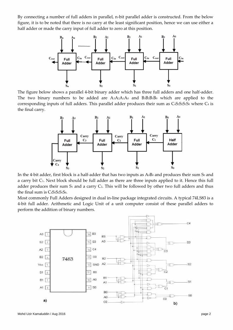
By connecting a number of full adders in parallel, n-bit parallel adder is constructed. From the below
figure, it is to be noted that there is no carry at the least significant position, hence we can use either a
half adder or made the carry input of full adder to zero at this position.
The figure below shows a parallel 4-bit binary adder which has three full adders and one half-adder.
The two binary numbers to be added are A3A2A1A0 and B3B2B1B0 which are applied to the
corresponding inputs of full adders. This parallel adder produces their sum as C4S3S2S1S0 where C4 is
the final carry.
In the 4-bit adder, first block is a half-adder that has two inputs as A0B0 and produces their sum S0 and
a carry bit C1. Next block should be full adder as there are three inputs applied to it. Hence this full
adder produces their sum S1 and a carry C2. This will be followed by other two full adders and thus
the final sum is C4S3S2S1S0.
Most commonly Full Adders designed in dual in-line package integrated circuits. A typical 74LS83 is a
4-bit full adder. Arithmetic and Logic Unit of a unit computer consist of these parallel adders to
perform the addition of binary numbers.
Mohd Uzir Kamaluddin / Aug 2016 page 3
2. Subtractor
Subtractor is a circuit which is used to subtract two binary number (digit) and provides Difference and
Borrow as output.
Half Subtractor is used for subtracting one single bit binary digit from another single bit binary digit.
A logic circuit which is used for subtracting three single bit binary digit is known as Full Subtractor.
Parallel Binary Subtractors
To perform the subtraction of binary numbers with more than one bit is performed through the
parallel subtractors. This parallel subtractor can be designed in several ways, including combination of
half and full subtractors, all full subtractors, all full adders with subtrahend complement input, etc.
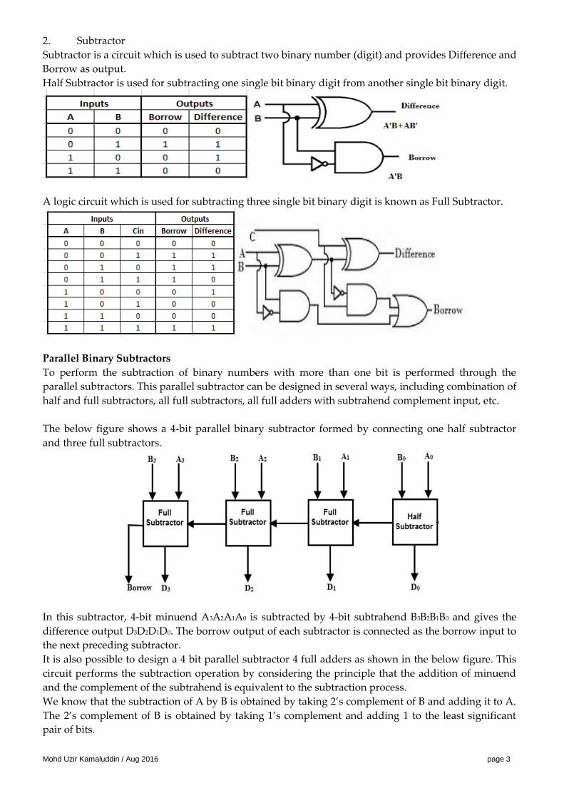
The below figure shows a 4-bit parallel binary subtractor formed by connecting one half subtractor
and three full subtractors.
In this subtractor, 4-bit minuend A3A2A1A0 is subtracted by 4-bit subtrahend B3B2B1B0 and gives the
difference output D3D2D1D0. The borrow output of each subtractor is connected as the borrow input to
the next preceding subtractor.
It is also possible to design a 4 bit parallel subtractor 4 full adders as shown in the below figure. This
circuit performs the subtraction operation by considering the principle that the addition of minuend
and the complement of the subtrahend is equivalent to the subtraction process.
We know that the subtraction of A by B is obtained by taking 2’s complement of B and adding it to A.
The 2’s complement of B is obtained by taking 1’s complement and adding 1 to the least significant
pair of bits.

Mohd Uzir Kamaluddin / Aug 2016 page 4
Hence, in this circuit 1’s complement of B is obtained with the inverters (NOT gate) and a 1 can be
added to the sum through the input carry.
Parallel Adder / Subtractor
The operations of both addition and subtraction can be performed by a one common binary adder.
Such binary circuit can be designed by adding an Ex-OR gate with each full adder as shown in below
figure. The figure below shows the 4-bit parallel binary adder/subtractor which has two 4 bit inputs as
A3A2A1A0 and B3B2B1B0.
The mode input control line M is connected with carry input of the least significant bit of the full
adder. This control line decides the type of operation, whether addition or subtraction.
When M = 1, the circuit is a subtractor and when M = 0, the circuit becomes adder. The Ex-OR gate
consists of two inputs to which one is connected to the B and other to input M. When M = 0, B Ex-OR
of 0 produce B. Then full adders add the B with A with carry input zero and hence an addition
operation is performed.
When M = 1, B Ex-OR of 0 produce B complement and also carry input is 1. Hence the complemented
B inputs are added to A and 1 is added through the input carry, nothing but a 2’s complement
operation. Therefore, the subtraction operation is performed.
Note: BB 0 and BB 1
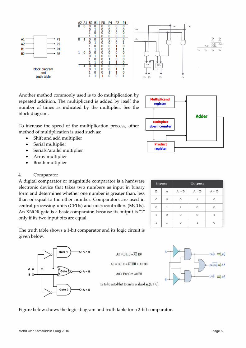
3. Multiplier
A binary multiplier is an electronic circuit used in digital electronics, such as a computer, to multiply
two binary numbers. It is built using binary adders. A simple 2-bit multiplier, A2A1 x B2B1 can be
designed using logic gates as shown in the truth table below.
Mohd Uzir Kamaluddin / Aug 2016 page 5
Another method commonly used is to do multiplication by
repeated addition. The multiplicand is added by itself the
number of times as indicated by the multiplier. See the
block diagram.
To increase the speed of the multiplication process, other
method of multiplication is used such as:
Shift and add multiplier
Serial multiplier
Serial/Parallel multiplier
Array multiplier
Booth multiplier
4. Comparator
A digital comparator or magnitude comparator is a hardware
electronic device that takes two numbers as input in binary
form and determines whether one number is greater than, less
than or equal to the other number. Comparators are used in
central processing units (CPUs) and microcontrollers (MCUs).
An XNOR gate is a basic comparator, because its output is "1"
only if its two input bits are equal.
The truth table shows a 1-bit comparator and its logic circuit is
given below.
Figure below shows the logic diagram and truth table for a 2-bit comparator.

Mohd Uzir Kamaluddin / Aug 2016 page 6
A 4-bit magnitude comparator TTL 74LS85.
An 8-bit word comparator.
For comparators that compares 3 bits or more, the truth table method of designing comparators will
result in a huge truth table.
Design of a 4-bit comparator using the deduction method.

Mohd Uzir Kamaluddin / Aug 2016 page 7
5. Decoders and Encoders
In digital electronics, a decoder can take the form of a multiple-input, multiple-output logic circuit
that converts coded inputs into coded outputs, where the input and output codes are different. e.g. n-
to-2n, binary-coded decimal decoders. Enable inputs must be on for the decoder to function, otherwise
its outputs assume a single "disabled" output code word. Decoding is necessary in applications such as
data multiplexing, 7 segment display and memory address decoding.
The example decoder circuit would be an AND gate because the output of an AND gate is "High" (1)
only when all its inputs are "High." Such output is called as "active High output". If instead of AND
gate, the NAND gate is connected the output will be "Low" (0) only when all its inputs are "High".
Such output is called as "active low output".
The diagram below shows the 2 to 4 binary decoder with active HIGH output.

Mohd Uzir Kamaluddin / Aug 2016 page 8
The IC Decoder 74LS138 is shown in the diagram. It is a 3 to 8
decoder, with active high output. Some binary decoders have an
additional input pin labelled “Enable” that controls the outputs
from the device. This extra input allows the decoders outputs to
be turned “ON” or “OFF” as required. These types of binary
decoders are commonly used as “memory address decoders” in
microprocessor memory applications.
A 4 to 16 decoder can be designed using two 3 to 8 decoders as shown.
But some binary decoders are constructed using NAND gates instead of AND gates for their decoded
output, since NAND gates are cheaper to produce than AND’s as they require fewer transistors to
implement within their design.
The use of NAND gates as the decoding element, results in an active-“LOW” output while the rest
will be “HIGH”. As a NAND gate produces the AND operation with an inverted output, the NAND
decoder looks like this with its inverted truth table.

Mohd Uzir Kamaluddin / Aug 2016 page 9
An encoder is a digital function that performs the inverse operation of a decoder. An encoder has 2n
(or fewer) input lines and n output lines. The output lines generate the binary code corresponding to
the input value.
One of the main disadvantages of standard digital encoders is that they can generate the wrong
output code when there is more than one input present at logic level “1”.
One simple way to overcome this problem is to “Prioritize” the level of each input pin and if there was
more than one input at logic level “1” the actual output code would only correspond to the input with
the highest designated priority. Then this type of digital encoder is known commonly as a Priority
Encoder or P-encoder for short.
Mohd Uzir Kamaluddin / Aug 2016 page 10
6. Multiplexer (MUX) and De-Multiplexer (DEMUX)
A multiplexer or MUX is a device that performs multiplexing; it selects one of many analog or digital
input signals and forwards the selected input into a single output line. A multiplexer of 2n inputs has n
select bits, which are used to select which input line to send to the
output.
A multiplexer makes it possible for several signals to share one
device or resource, for example one A/D converter or one
communication line, instead of having one device per input signal.
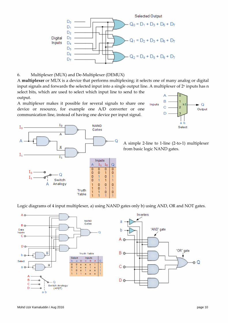
A simple 2-line to 1-line (2-to-1) multiplexer
from basic logic NAND gates.
Logic diagrams of 4 input multiplexer, a) using NAND gates only b) using AND, OR and NOT gates.

Mohd Uzir Kamaluddin / Aug 2016 page 11
A de-multiplexer (or DEMUX) is a device taking a single input signal and
selecting one of many data-output-lines, which is connected to the single
input. A multiplexer is often used with a complementary de-multiplexer
on the receiving end. A DEMUX is also known as data distributor.
The 1 to 4 DEMUX can be designed using logic gates as
shown.
Another way to implement a 1 to 4
DEMUX is by using a 2 to 4 decoder with
AND gates as shown.

Mohd Uzir Kamaluddin / Aug 2016 page 12
Implementation of logic functions using:
1. Decoder
A decoder can be used to implement logic functions. Since
all the minterms of the function are available at the output
then there is no need for simplification. All is needed is an
OR gate for each function to sum the required minterms.
As an example, implement the following functions using
an appropriate decoder and OR gates.
S(x,y,z) = ∑m(1,2,4,7) and C(x,y,z) = ∑m(3,5,6,7)
The implementation using 3 to 8 decoder active high
output and OR gates is as shown.
If an active low output decoder is used,
the implementation uses a NAND gate.
2. 7-segment decoder/driver
A seven-segment display is a form of electronic display device for
displaying decimal numerals that is an alternative to the more complex dot-
matrix displays. Seven-segment displays are widely used in digital clocks,
electronic meters, and other electronic devices for displaying numerical
information.
The common way of driving the 7-segment display is
by the use of a special IC called the 7-segment
decoder/driver. This IC receives input as BCD and
output the 7-segment codes for the 7-segment
display. The 74LS47 has active-low outputs, and can
only be used to drive common anode 7-segment
display unit.
BCD input Display
0011 3
0101 5
1001 9
3. Multiplexer
A multiplexer can also be used to implement logic functions. There are a few ways to design such
circuit, depending on the multiplexer used. Consider the function: CABCBACBAf ),,(
a) Using an 8 to 1 multiplexer

Mohd Uzir Kamaluddin / Aug 2016 page 13
The function f(A,B,C) is tabulated in the form of truth table, and then the logic function is
implemented directly using the 8-1 multiplexer.
A B C f
0 0 0 0
0 0 1 1
0 1 0 1
0 1 1 1
1 0 0 0
1 0 1 0
1 1 0 0
1 1 1 1
b) Using a 4 to 1 multiplexer
For this design, the input A and B is connected to the select lines C1 and C2. The expression for
mux input is obtained by comparing the output f with the input which is not used, that is C.
Thus the method is called residue method.
A B C f MUX Input
0 0 0 0
I0 = C
0 0 1 1
0 1 0 1
I1 = 1
0 1 1 1
1 0 0 0
I2 = 0
1 0 1 0
1 1 0 0
I3 = C
1 1 1 1
Exercise 1
a) Draw the truth table of a full adder.
b) Write down the Boolean expression for the sum and carry output.
c) Draw the logic diagram using NAND gates only.
d) Implement the full adder using 3-to-8 active high output decoder.
e) Implement a full adder using only 4-to-1 multiplexers.
Exercise 2
a) Draw the logic circuit of the following function using a 3-to-8 active high output decoder.
F = ∑m(1 ,2, 4, 6, 7)
b) Draw the logic circuit of the following function using a 3-to-8 active low output decoder.
F = ∑m(0 ,2, 3, 5, 6)
Exercise 3
A Boolean function F of four variables A, B, C and D is given by the sum of minterms:
F = ∑m(1 ,2, 4, 7, 8, 10, 12, 14)
a) Implement the function F using a 16-to-1 line multiplexer.
b) Implement the function F using an 8-to-1 line multiplexer.
c) Implement the function F using a 4-to-1 line multiplexer.
Mohd Uzir Kamaluddin / Aug 2016 page 14
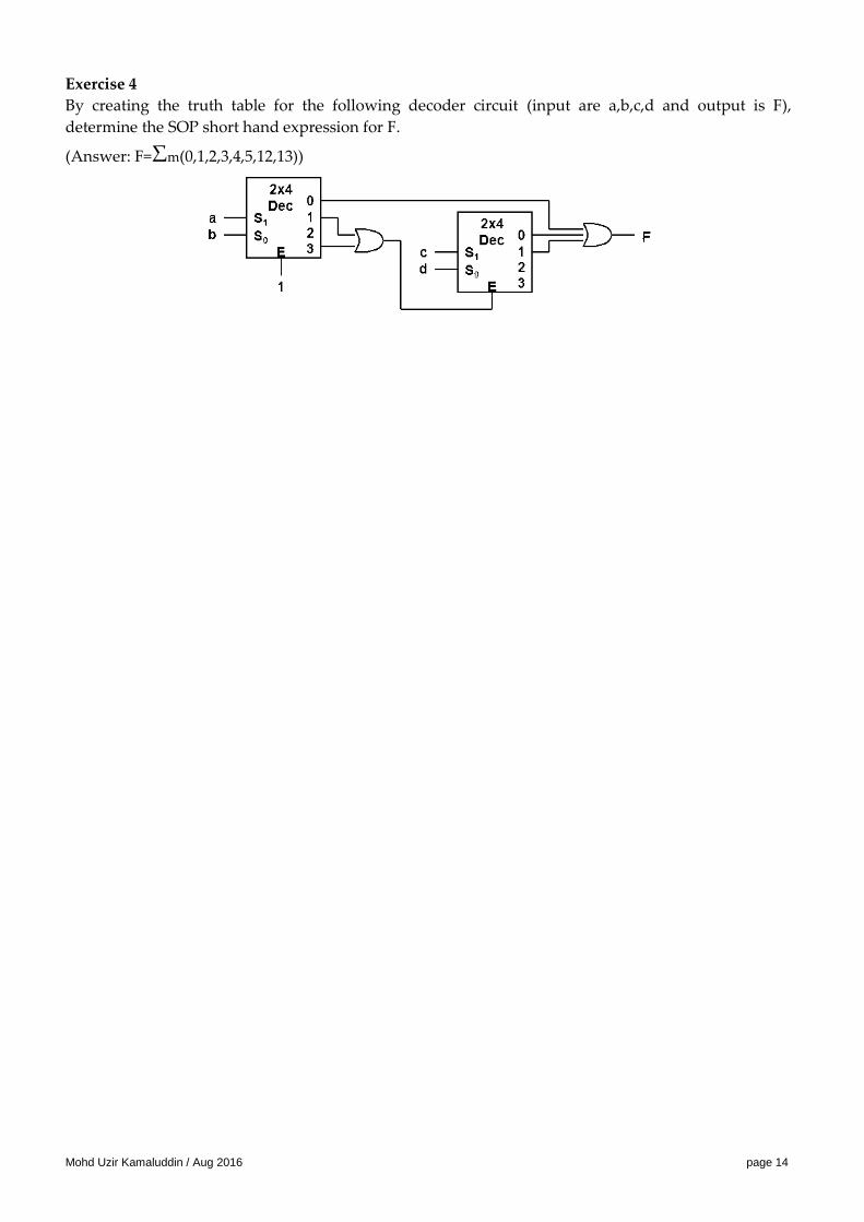
Exercise 4
By creating the truth table for the following decoder circuit (input are a,b,c,d and output is F),
determine the SOP short hand expression for F.
(Answer: F=Σm(0,1,2,3,4,5,12,13))