DIGITAL SIGNAL PROCESSING LAB - Muffakham Jah ...mjcollege.ac.in/images/labmannuals/IV EEE II SEM...
94
MUFFAK ENGINEE Banjara ELECTRICA LA DIGITAL S IV KHAM JAH COLLEGE ERING & TECHNOLO a Hills Road No 3, Hyderabad- 34 www.mjcollege.ac.in AL ENGINEERING DEPARTM ABORATORY MANUAL SIGNAL PROCESSING For V/IV B.E II SEM EEE/EIE Prepared by Mohd. Abdul Muqeet Assoc. Professor, EED E OF OGY MENT G LAB
-
Upload
trinhkhuong -
Category
Documents
-
view
233 -
download
1
Transcript of DIGITAL SIGNAL PROCESSING LAB - Muffakham Jah ...mjcollege.ac.in/images/labmannuals/IV EEE II SEM...
MUFFAKHAM JAH COLLEGE OFENGINEERING & TECHNOLOGY
Banjara Hills Road No 3, Hyderabad
ELECTRICAL ENGINEERING
LABORATORY MANUAL
DIGITAL SIGNAL
IV/IV B.E I
MUFFAKHAM JAH COLLEGE OFENGINEERING & TECHNOLOGY
Banjara Hills Road No 3, Hyderabad- 34 www.mjcollege.ac.in
ELECTRICAL ENGINEERING DEPARTMENT
LABORATORY MANUAL
DIGITAL SIGNAL PROCESSING LAB
For
IV/IV B.E II SEM EEE/EIE
Prepared by
Mohd. Abdul Muqeet Assoc. Professor, EED
MUFFAKHAM JAH COLLEGE OF ENGINEERING & TECHNOLOGY
DEPARTMENT
PROCESSING LAB

Digital Signal Processing Lab Manual
1
Prepared By: Mohd.Abdul Muqeet
WITH EFFECT FROM THE ACADEMIC YEAR 2013-2014
EE 481
DSP LAB
(COMMON TO EEE & IE)
Instruction 3 Periods per week
Duration of University Examination 3 Hours
University Examination 50 Marks
Sessional 25 Marks
1. Waveform generation -Square, Triangular and Trapezoidal.
2. Verification of Convolution Theorem-comparison Circular and
Linear Convolutions.
3. Computation of DFT, IDFT using Direct and FFT methods.
4. Verification of Sampling Theorem
5. Design of Butterworth and Chebyshev of LP & HP filters.
6. Design of LPF using rectangular and Hamming, Kaiser
Windows.
7. 16 bit Addition, Integer and fractional multiplication on 2407
DSP Trainer kit.
8. Generation of sine wave and square wave using DSP trainer
kit.
9. Response of Low pass and High pass filters using DSP trainer
kit.
10. Linear convolution using DSP trainer kit.
11. PWM Generation on DSP trainer kit.
12. Key pad interfacing with DSP.
13. LED interfacing with DSP.
14. Stepper Motor Control using DSP.
15. DC Motor 4- quadrant speed control using DSP.
16. Three phase 1M speed control using DSP.
17. Brushless DC Motor Control.
At least ten experiments should be completed in the semester
Digital Signal Processing Lab Manual
2
Prepared By: Mohd.Abdul Muqeet
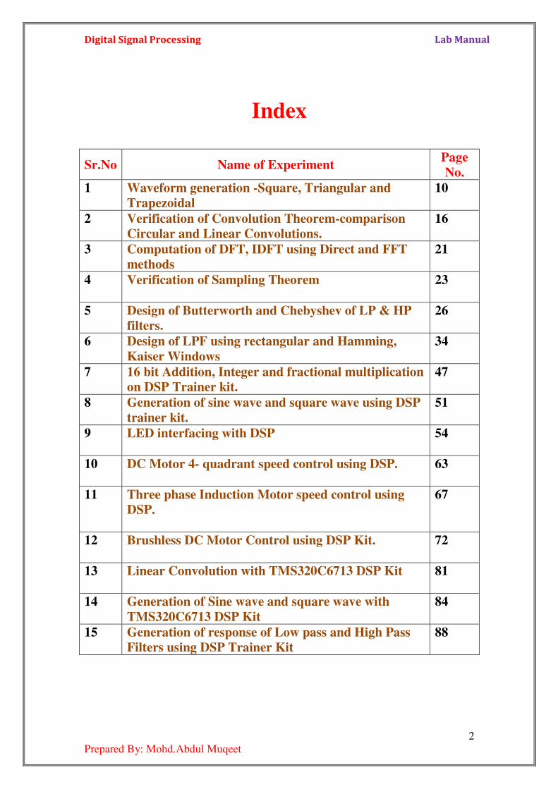
Index
Sr.No Name of Experiment
Page
No.
1 Waveform generation -Square, Triangular and
Trapezoidal
10
2 Verification of Convolution Theorem-comparison
Circular and Linear Convolutions.
16
3 Computation of DFT, IDFT using Direct and FFT
methods
21
4 Verification of Sampling Theorem
23
5 Design of Butterworth and Chebyshev of LP & HP
filters.
26
6 Design of LPF using rectangular and Hamming,
Kaiser Windows
34
7 16 bit Addition, Integer and fractional multiplication
on DSP Trainer kit.
47
8 Generation of sine wave and square wave using DSP
trainer kit.
51
9 LED interfacing with DSP
54
10 DC Motor 4- quadrant speed control using DSP.
63
11 Three phase Induction Motor speed control using
DSP.
67
12 Brushless DC Motor Control using DSP Kit.
72
13 Linear Convolution with TMS320C6713 DSP Kit
81
14 Generation of Sine wave and square wave with
TMS320C6713 DSP Kit
84
15 Generation of response of Low pass and High Pass
Filters using DSP Trainer Kit
88
Digital Signal Processing Lab Manual
3
Prepared By: Mohd.Abdul Muqeet
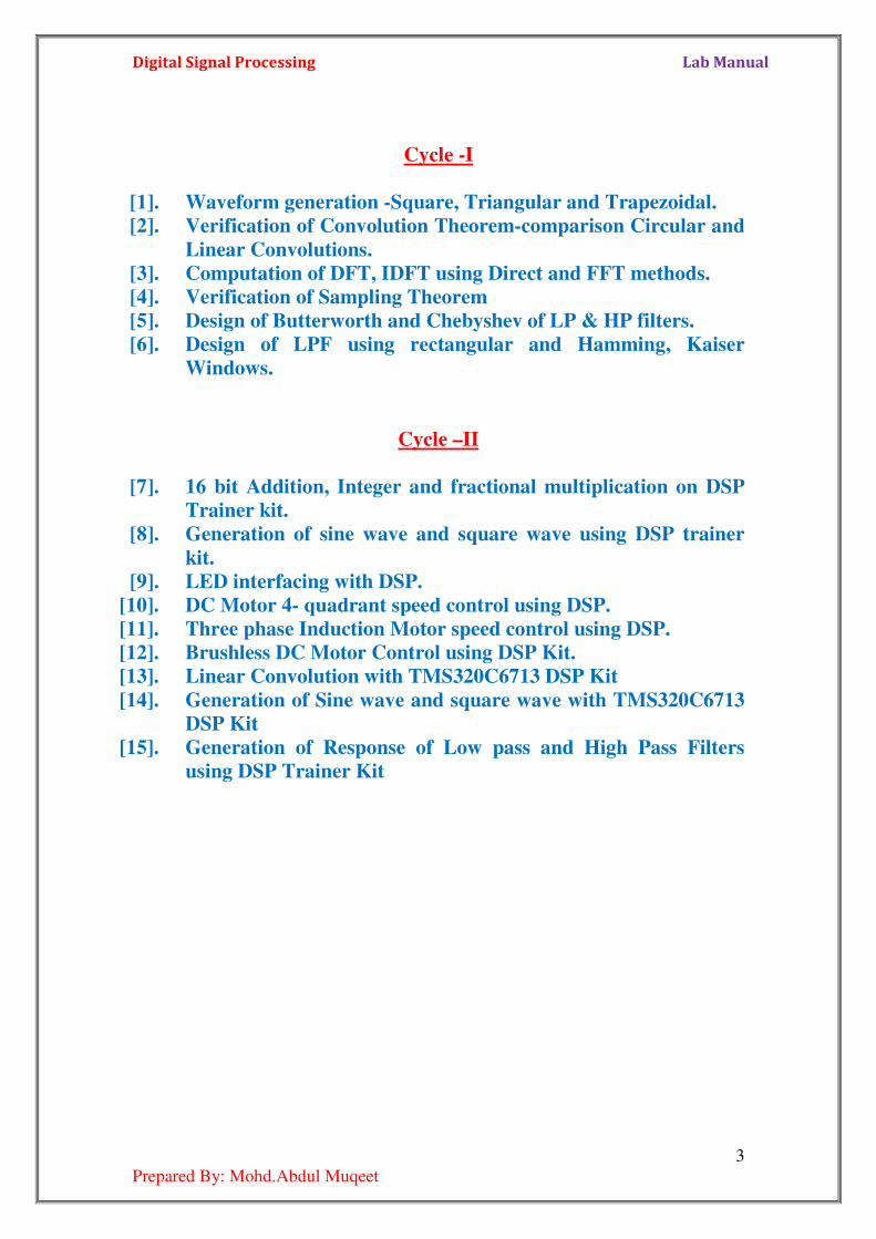
Cycle -I
[1]. Waveform generation -Square, Triangular and Trapezoidal.
[2]. Verification of Convolution Theorem-comparison Circular and
Linear Convolutions.
[3]. Computation of DFT, IDFT using Direct and FFT methods.
[4]. Verification of Sampling Theorem
[5]. Design of Butterworth and Chebyshev of LP & HP filters.
[6]. Design of LPF using rectangular and Hamming, Kaiser
Windows.
Cycle –II
[7]. 16 bit Addition, Integer and fractional multiplication on DSP
Trainer kit.
[8]. Generation of sine wave and square wave using DSP trainer
kit.
[9]. LED interfacing with DSP.
[10]. DC Motor 4- quadrant speed control using DSP.
[11]. Three phase Induction Motor speed control using DSP.
[12]. Brushless DC Motor Control using DSP Kit.
[13]. Linear Convolution with TMS320C6713 DSP Kit
[14]. Generation of Sine wave and square wave with TMS320C6713
DSP Kit
[15]. Generation of Response of Low pass and High Pass Filters
using DSP Trainer Kit
Digital Signal Processing Lab Manual
4
Prepared By: Mohd.Abdul Muqeet
Cycle-I
Digital Signal Processing Lab Manual
5
Prepared By: Mohd.Abdul Muqeet
INTRODUCTION
MATLAB, which stands for MATrix LABoratory, is a state-of-the-art
mathematical software package for high performance numerical computation and
visualization provides an interactive environment with hundreds of built in functions
for technical computation, graphics and animation and is used extensively in both
academia and industry. It is an interactive program for numerical computation and
data visualization, which along with its programming capabilities provides a very
useful tool for almost all areas of science and engineering.
At its core ,MATLAB is essentially a set (a “toolbox”) of routines (called “m
files” or “mex files”) that sit on your computer and a window that allows you to create
new variables with names (e.g. voltage and time) and process those variables with any
of those routines (e.g. plot voltage against time, find the largest voltage, etc).
It also allows you to put a list of your processing requests together in a file and save
that combined list with a name so that you can run all of those commands in the same
order at some later time. Furthermore, it allows you to run such lists of commands
such that you pass in data.
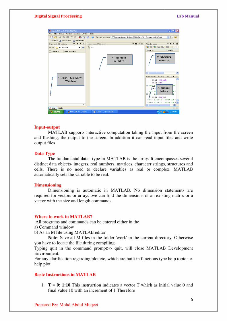
MATLAB Windows:
MATLAB works with through these basic windows
Command Window This is the main window .it is characterized by MATLAB command prompt
>> when you launch the application program MATLAB puts you in this window all
commands including those for user-written programs ,are typed in this window at the
MATLAB prompt
The Current Directory Window The Current Directory window displays a current directory with a listing of its
contents. There is navigation capability for resetting the current directory to any
directory among those set in the path. This window is useful for finding the location
of particular files and scripts so that they can be edited, moved, renamed, deleted, etc.
The default current directory is the Work subdirectory of the original MATLAB
installation directory
The Command History Window The Command History window, at the lower left in the default desktop,
contains a log of commands that have been executed within the Command window.
This is a convenient feature for tracking when developing or debugging programs or
to confirm that commands were executed in a particular sequence during a multistep
calculation from the command line.
Graphics Window The output of all graphics commands typed in the command window are
flushed to the graphics or figure window, a separate gray window with white
background color the user can create as many windows as the system memory will
allow.
Edit Window This is where you write edit, create and save your own programs in files called
M files.
Digital Signal Processing
Prepared By: Mohd.Abdul Muqeet
Input-output MATLAB supports interactive computation taking the input from the screen
and flushing, the output to the screen. In addition it can read input files and write
output files
Data Type The fundamental data
distinct data objects- integers, real numbers, matrices, character strings, structures and
cells. There is no need to declare variables as real or complex, MATLAB
automatically sets the variable to be real.
Dimensioning Dimensioning is automatic in MAT
required for vectors or arrays .we can find the dimensions of an existing matrix or a
vector with the size and length commands.
Where to work in MATLAB? All programs and commands can be entered either in the
a) Command window
b) As an M file using MATLAB editor
Note: Save all M files in the folder 'work' in the current directory. Otherwise
you have to locate the file during compiling.
Typing quit in the command prompt>> quit, will close MATLAB Development
Environment.
For any clarification regarding plot etc, which are built in functions type help topic i.e.
help plot
Basic Instructions in MATLAB
1. T = 0: 1:10 This instruction indicates a vector T which as initial value 0 and
final value 10 with an increment of 1 Ther
Prepared By: Mohd.Abdul Muqeet
MATLAB supports interactive computation taking the input from the screen
and flushing, the output to the screen. In addition it can read input files and write
The fundamental data –type in MATLAB is the array. It encompasses severa
integers, real numbers, matrices, character strings, structures and
cells. There is no need to declare variables as real or complex, MATLAB
automatically sets the variable to be real.
Dimensioning is automatic in MATLAB. No dimension statements are
required for vectors or arrays .we can find the dimensions of an existing matrix or a
vector with the size and length commands.
Where to work in MATLAB? All programs and commands can be entered either in the
b) As an M file using MATLAB editor
: Save all M files in the folder 'work' in the current directory. Otherwise
you have to locate the file during compiling.
Typing quit in the command prompt>> quit, will close MATLAB Development
For any clarification regarding plot etc, which are built in functions type help topic i.e.
MATLAB
This instruction indicates a vector T which as initial value 0 and
final value 10 with an increment of 1 Therefore
Lab Manual
6
MATLAB supports interactive computation taking the input from the screen
and flushing, the output to the screen. In addition it can read input files and write
type in MATLAB is the array. It encompasses several
integers, real numbers, matrices, character strings, structures and
cells. There is no need to declare variables as real or complex, MATLAB
LAB. No dimension statements are
required for vectors or arrays .we can find the dimensions of an existing matrix or a
: Save all M files in the folder 'work' in the current directory. Otherwise
Typing quit in the command prompt>> quit, will close MATLAB Development
For any clarification regarding plot etc, which are built in functions type help topic i.e.
This instruction indicates a vector T which as initial value 0 and
Digital Signal Processing Lab Manual
7
Prepared By: Mohd.Abdul Muqeet
T = [0 1 2 3 4 5 6 7 8 9 10]
2. F= 20: 1: 100 F = [20 21 22 23 24 ……… 100]
3. T= 0:1/ pi: 1 T= [0, 0.3183, 0.6366, 0.9549]
4. zeros (1, 3) The above instruction creates a vector of one row and three
columns whose values are zero Output= [0 0 0]
5. Transpose a vector Suppose T= [1 2 3],
Then transpose T’= 1
2 3
6. Empty vector Y = []
Y =
[]
6. Matrix Operation
a)If a = [ 1 2 3] b = [4 5 6]
a.*b = [4 10 18] b)If v = [0:2:8]
v = [0 2 4 6 8]
v(1:3) ans [0 2 4]
v(1:2:4)
ans[ 0 4]
c) A = [1 2 3; 3 4 5; 6 7 8]
A =
1 2 3
3 4 5
6 7 8
A(2,3) ans 5
A(1:2,2:3)
ans =
2 3
4 5
A(:,2)
ans =
2
4
7
A(3,:)
ans =
6 7 8
Operations on vector and matrices in MATLAB
MATLAB utilizes the following arithmetic operators;
Digital Signal Processing Lab Manual
8
Prepared By: Mohd.Abdul Muqeet
+ Addition
- Subtraction
* Multiplication
/ Division
^ Power Operator
‘ transpose
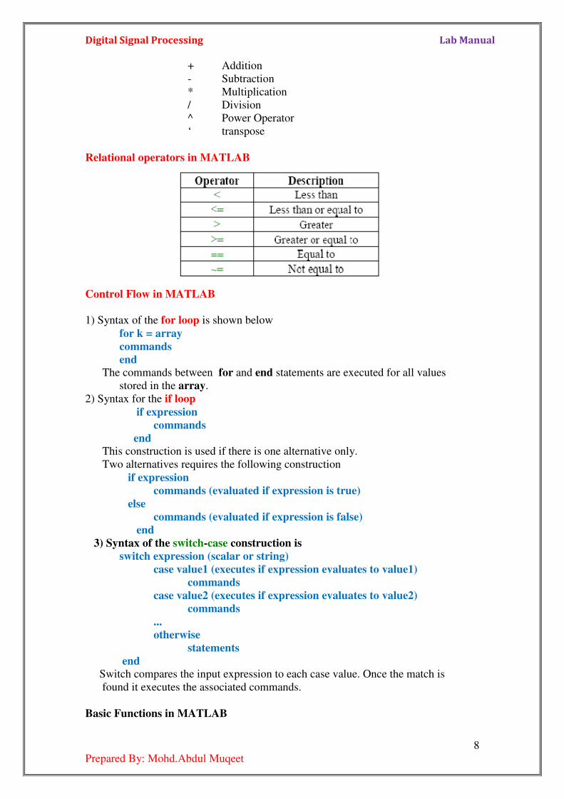
Relational operators in MATLAB
Control Flow in MATLAB
1) Syntax of the for loop is shown below
for k = array
commands
end The commands between for and end statements are executed for all values
stored in the array.
2) Syntax for the if loop
if expression
commands
end This construction is used if there is one alternative only.
Two alternatives requires the following construction
if expression
commands (evaluated if expression is true)
else
commands (evaluated if expression is false)
end
3) Syntax of the switch-case construction is
switch expression (scalar or string)
case value1 (executes if expression evaluates to value1)
commands
case value2 (executes if expression evaluates to value2)
commands
...
otherwise
statements
end Switch compares the input expression to each case value. Once the match is
found it executes the associated commands.
Basic Functions in MATLAB
Digital Signal Processing Lab Manual
9
Prepared By: Mohd.Abdul Muqeet
1) Plot Syntax: plot (x,y)
Plots vector y versus vector x. If x or y is a matrix, then the vector is plotted
versus the rows or columns of the matrix.
2) Stem Syntax: stem(Y)
Discrete sequence or "stem" plot.
Stem (Y) plots the data sequence Y as stems from the x axis terminated with
circles for the data value. If Y is a matrix then each column is plotted as a
separate series.
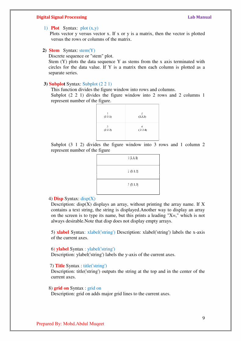
3) Subplot Syntax: Subplot (2 2 1)
This function divides the figure window into rows and columns.
Subplot (2 2 1) divides the figure window into 2 rows and 2 columns 1
represent number of the figure.
Subplot (3 1 2) divides the figure window into 3 rows and 1 column 2
represent number of the figure
4) Disp Syntax: disp(X)
Description: disp(X) displays an array, without printing the array name. If X
contains a text string, the string is displayed.Another way to display an array
on the screen is to type its name, but this prints a leading "X=," which is not
always desirable.Note that disp does not display empty arrays.
5) xlabel Syntax: xlabel('string') Description: xlabel('string') labels the x-axis
of the current axes.
6) ylabel Syntax : ylabel('string')
Description: ylabel('string') labels the y-axis of the current axes.
7) Title Syntax : title('string')
Description: title('string') outputs the string at the top and in the center of the
current axes.
8) grid on Syntax : grid on
Description: grid on adds major grid lines to the current axes.
Digital Signal Processing Lab Manual
10
Prepared By: Mohd.Abdul Muqeet
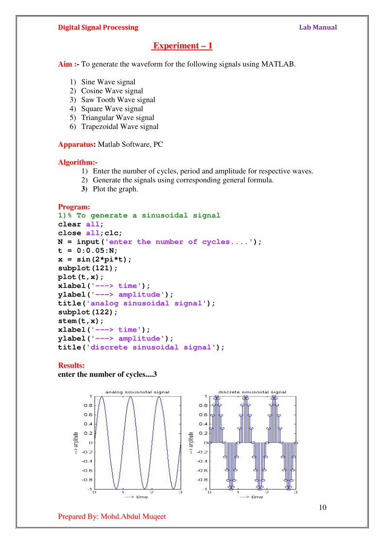
Experiment – 1 Aim :- To generate the waveform for the following signals using MATLAB.
1) Sine Wave signal
2) Cosine Wave signal
3) Saw Tooth Wave signal
4) Square Wave signal
5) Triangular Wave signal
6) Trapezoidal Wave signal
Apparatus: Matlab Software, PC
Algorithm:- 1) Enter the number of cycles, period and amplitude for respective waves.
2) Generate the signals using corresponding general formula.
3) Plot the graph.
Program: 1)% To generate a sinusoidal signal
clear all;
close all;clc;
N = input('enter the number of cycles....');
t = 0:0.05:N;
x = sin(2*pi*t);
subplot(121);
plot(t,x);
xlabel('---> time');
ylabel('---> amplitude');
title('analog sinusoidal signal');
subplot(122);
stem(t,x);
xlabel('---> time');
ylabel('---> amplitude');
title('discrete sinusoidal signal');
Results:
enter the number of cycles....3
Digital Signal Processing Lab Manual
11
Prepared By: Mohd.Abdul Muqeet
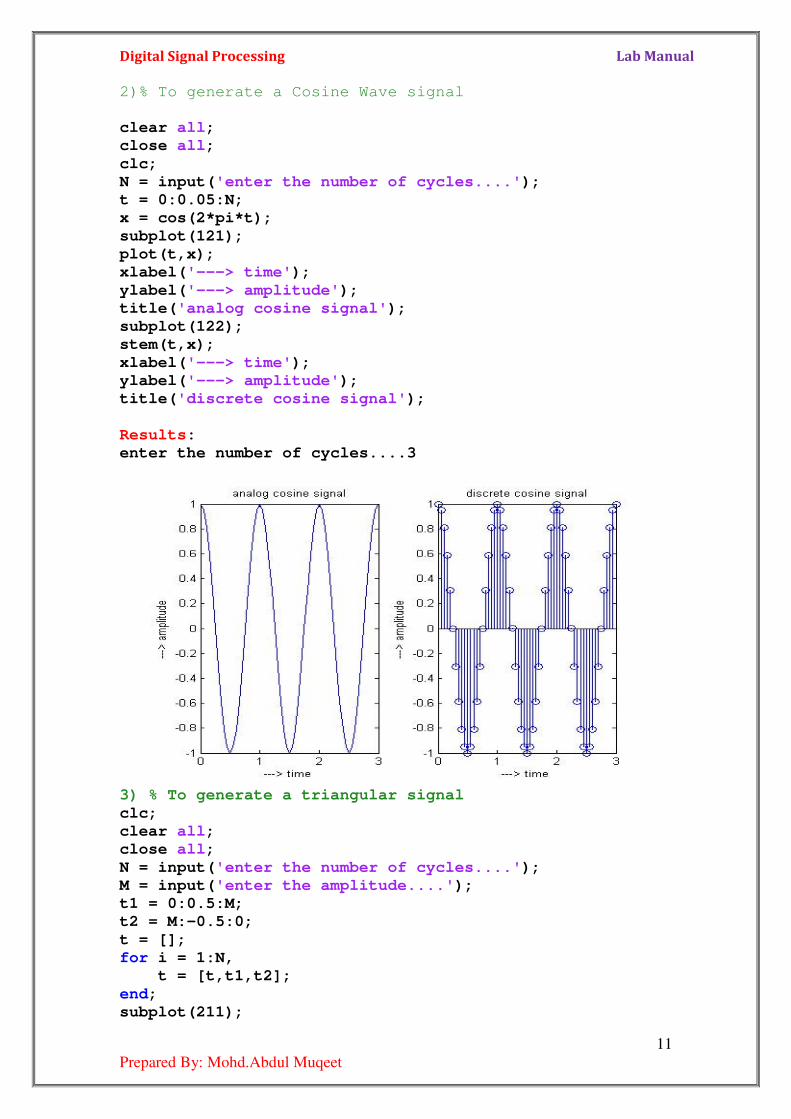
2)% To generate a Cosine Wave signal
clear all;
close all;
clc;
N = input('enter the number of cycles....');
t = 0:0.05:N;
x = cos(2*pi*t);
subplot(121);
plot(t,x);
xlabel('---> time');
ylabel('---> amplitude');
title('analog cosine signal');
subplot(122);
stem(t,x);
xlabel('---> time');
ylabel('---> amplitude');
title('discrete cosine signal');
Results:
enter the number of cycles....3
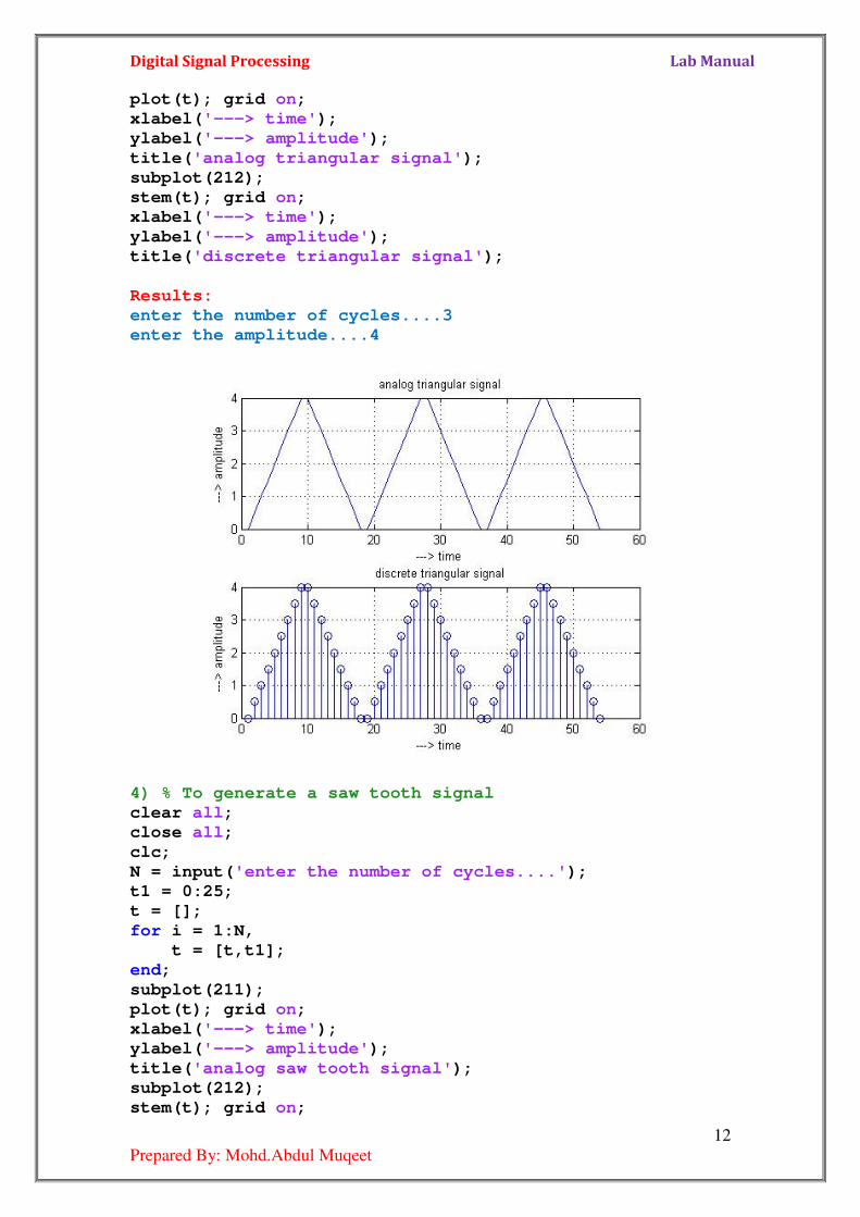
3) % To generate a triangular signal
clc;
clear all;
close all;
N = input('enter the number of cycles....');
M = input('enter the amplitude....');
t1 = 0:0.5:M;
t2 = M:-0.5:0;
t = [];
for i = 1:N,
t = [t,t1,t2];
end;
subplot(211);
Digital Signal Processing Lab Manual
12
Prepared By: Mohd.Abdul Muqeet
plot(t); grid on;
xlabel('---> time');
ylabel('---> amplitude');
title('analog triangular signal');
subplot(212);
stem(t); grid on;
xlabel('---> time');
ylabel('---> amplitude');
title('discrete triangular signal');
Results:
enter the number of cycles....3
enter the amplitude....4
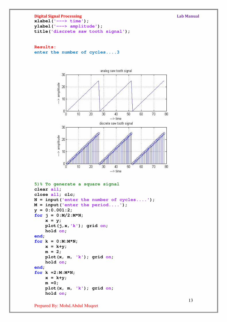
4) % To generate a saw tooth signal
clear all;
close all;
clc;
N = input('enter the number of cycles....');
t1 = 0:25;
t = [];
for i = 1:N,
t = [t,t1];
end;
subplot(211);
plot(t); grid on;
xlabel('---> time');
ylabel('---> amplitude');
title('analog saw tooth signal');
subplot(212);
stem(t); grid on;
Digital Signal Processing Lab Manual
13
Prepared By: Mohd.Abdul Muqeet
xlabel('---> time');
ylabel('---> amplitude');
title('discrete saw tooth signal');
Results:
enter the number of cycles....3
5)% To generate a square signal
clear all;
close all; clc;
N = input('enter the number of cycles....');
M = input('enter the period....');
y = 0:0.001:2;
for j = 0:M/2:M*N;
x = y;
plot(j,x,'k'); grid on;
hold on;
end;
for k = 0:M:M*N;
x = k+y;
m = 2;
plot(x, m, 'k'); grid on;
hold on;
end;
for k =2:M:M*N;
x = k+y;
m =0;
plot(x, m, 'k'); grid on;
hold on;

Digital Signal Processing Lab Manual
14
Prepared By: Mohd.Abdul Muqeet
end;
hold off;
axis([0 12 -0.5 2.5])
xlabel('---> time');
ylabel('---> amplitude');
title('Square signal');
Results: enter the number of cycles....4 enter the period....4
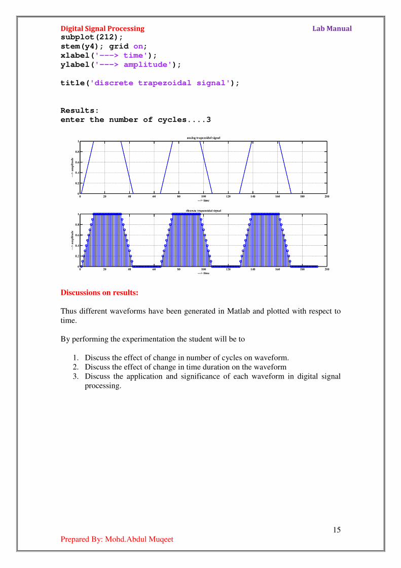
5)% To generate a Trapezoidal signal
clear all;
close all;
clc;
N = input('enter the number of cycles....');
LN=1;
x=0:0.1:LN; % 'x' is meant for linear rise %
a=length(x);
y=ones(1,a+10); % 'y' is meant for constancy %
z=LN:-0.1:0; % 'z' is meant for linear fall %
y3=[x y z ];
%y4=[y3 y3 y3 y3];
y4=[];
for i = 1:N,
y4=[y4,y3];
end;
subplot(211);
plot(y4); grid on;
xlabel('---> time');
ylabel('---> amplitude');
title('analog trapezoidal signal');
Digital Signal Processing Lab Manual
15
Prepared By: Mohd.Abdul Muqeet
subplot(212);
stem(y4); grid on;
xlabel('---> time');
ylabel('---> amplitude');
title('discrete trapezoidal signal');
Results:
enter the number of cycles....3
Discussions on results:
Thus different waveforms have been generated in Matlab and plotted with respect to
time.
By performing the experimentation the student will be to
1. Discuss the effect of change in number of cycles on waveform.
2. Discuss the effect of change in time duration on the waveform
3. Discuss the application and significance of each waveform in digital signal
processing.
Digital Signal Processing
Prepared By: Mohd.Abdul Muqeet
Aim: Write a Matlab program to
and Linear Convolutions.
a) Write a Matlab program to
Apparatus: Matlab Software, PC
Theory:
The mathematical definition of convolution in discrete time domain
where x[n] is input signal,
convolution. Here we multiply the terms of
and add them up.
In this equation, x(k), h(n
system at time n. Here one of the input is shifted in time by a value every time it is
multiplied with the other input signal. Linear Convolution is quite often used as a
method of implementing filters of various types.
Algorithm: 1) Give input sequence x[n].
2) Give impulse respo
3) Find the convolution y[n] using the matlab command CONV.
4) Plot x[n],h[n],y[n].
Program:
% MATLAB program for linear convolution
clc;
clear all;
close all;
disp('linear convolution program'
x=input('enter i/p x(n):'
m=length(x);
h=input('enter i/p h(n):'
n=length(h);
x=[x,zeros(1,n)];
subplot(2,2,1), stem(x);
title('i/p sequence x(n)is:'
xlabel('---->n');
ylabel('---->amplitude'
h=[h,zeros(1,m)];
subplot(2,2,2), stem(h);
title('i/p sequence h(n)is:'
xlabel('---->n');
ylabel('---->amplitude'
disp('convolution of x(n) & h(n) is y(n):'
y=zeros(1,m+n-1);
for i=1:m+n-1
Prepared By: Mohd.Abdul Muqeet
Experiment – 2
Write a Matlab program to verify Convolution Theorem-comparison
Write a Matlab program to implement and verify Linear Convolution
Matlab Software, PC
The mathematical definition of convolution in discrete time domain
is input signal, h[n] is impulse response, and y[n] is output. * denotes
convolution. Here we multiply the terms of x[k] by the terms of a time
In this equation, x(k), h(n-k) and y(n) represent the input to and output from the
re one of the input is shifted in time by a value every time it is
multiplied with the other input signal. Linear Convolution is quite often used as a
method of implementing filters of various types.
Give input sequence x[n].
Give impulse response sequence h[n].
Find the convolution y[n] using the matlab command CONV.
Plot x[n],h[n],y[n].
% MATLAB program for linear convolution
'linear convolution program');
'enter i/p x(n):');
'enter i/p h(n):');
subplot(2,2,1), stem(x);
'i/p sequence x(n)is:');
>amplitude');grid;
subplot(2,2,2), stem(h);
'i/p sequence h(n)is:');
>amplitude');grid;
'convolution of x(n) & h(n) is y(n):');
Lab Manual
16
comparison Circular
Linear Convolution.
The mathematical definition of convolution in discrete time domain
is output. * denotes
by the terms of a time-shifted h[n]
k) and y(n) represent the input to and output from the
re one of the input is shifted in time by a value every time it is
multiplied with the other input signal. Linear Convolution is quite often used as a

Digital Signal Processing
Prepared By: Mohd.Abdul Muqeet
y(i)=0;
for j=1:m+n-1
if(j<i+1)
y(i)=y(i)+x(j)*h(i
end
end
end
y
subplot(2,2,[3,4]),stem(y);
title('convolution of x(n) & h(n) is y(n):'
xlabel('---->n');
ylabel('---->amplitude'
Results: linear convolution programenter i/p x(n):[1 2 3 4 5]enter i/p h(n):[ 1 2]convolution of x(n) & h(n) is y(n): y = 1 4 7 10 13 10
Prepared By: Mohd.Abdul Muqeet
y(i)=y(i)+x(j)*h(i-j+1);
subplot(2,2,[3,4]),stem(y);
'convolution of x(n) & h(n) is y(n):');
>amplitude');grid;
linear convolution program enter i/p x(n):[1 2 3 4 5] enter i/p h(n):[ 1 2] convolution of x(n) & h(n) is y(n):
1 4 7 10 13 10
Lab Manual
17

Digital Signal Processing Lab Manual
18
Prepared By: Mohd.Abdul Muqeet
b) Write a Matlab program to implement and verify Circular convolution of two
given sequences.
Apparatus: Matlab Software, PC
Theory: Circular convolution is another way of finding the convolution sum of two
input signals. It resembles the linear convolution, except that the sample values of one
of the input signals is folded and right shifted before the convolution sum is found.
Also note that circular convolution could also be found by taking the DFT of the two
input signals and finding the product of the two frequency domain signals. The
Inverse DFT of the product would give the output of the signal in the time domain
which is the circular convolution output. The two input signals could have been of
varying sample lengths. But we take the DFT of higher point, which ever signals
levels to. For eg. If one of the signal is of length 256 and the other spans 51 samples,
then we could only take 256 point DFT. So the output of IDFT would be containing
256 samples instead of 306 samples, which follows N1+N2 – 1 where N1 & N2 are
the lengths 256 and 51 respectively of the two inputs. Thus the output which should
have been 306 samples long is fitted into 256 samples. The 256 points end up being a
distorted version of the correct signal. This process is called circular convolution.
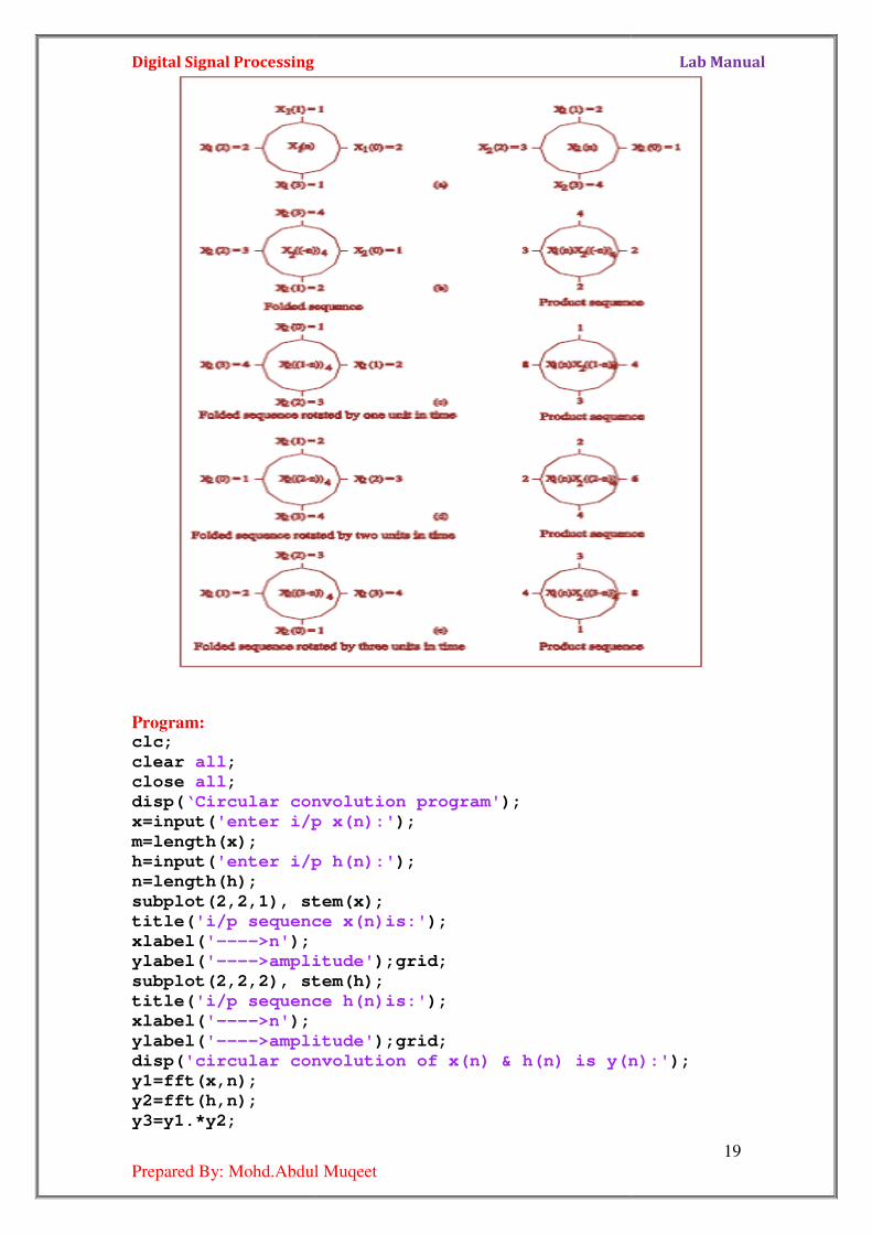
Circular convolution is explained using the following example.
The two sequences are
x1 (n) = 2,1,2,1
x2 (n) = 1,2,3,4
Each sequence consists of four nonzero points. For purpose of illustrating the
operations involved in circular convolution it is desirable to graph each sequence as
points on a circle. Thus the sequences x1 (n) and x2 (n) are graphed as illustrated in
the fig.We note that the sequences are graphed in a counterclockwise direction on a
circle.This stablishes the reference direction in rotating one of sequences relative to
the other. Now, y (m) is obtained by circularly convolving x (n) with h (n).
Algorithm:
1) Give input sequence x[n].
2) Give impulse response sequence h[n].
3) Find the Circular Convolution y[n] using the DFT method.
4) Plot x[n],h[n],y[n].
Digital Signal Processing
Prepared By: Mohd.Abdul Muqeet
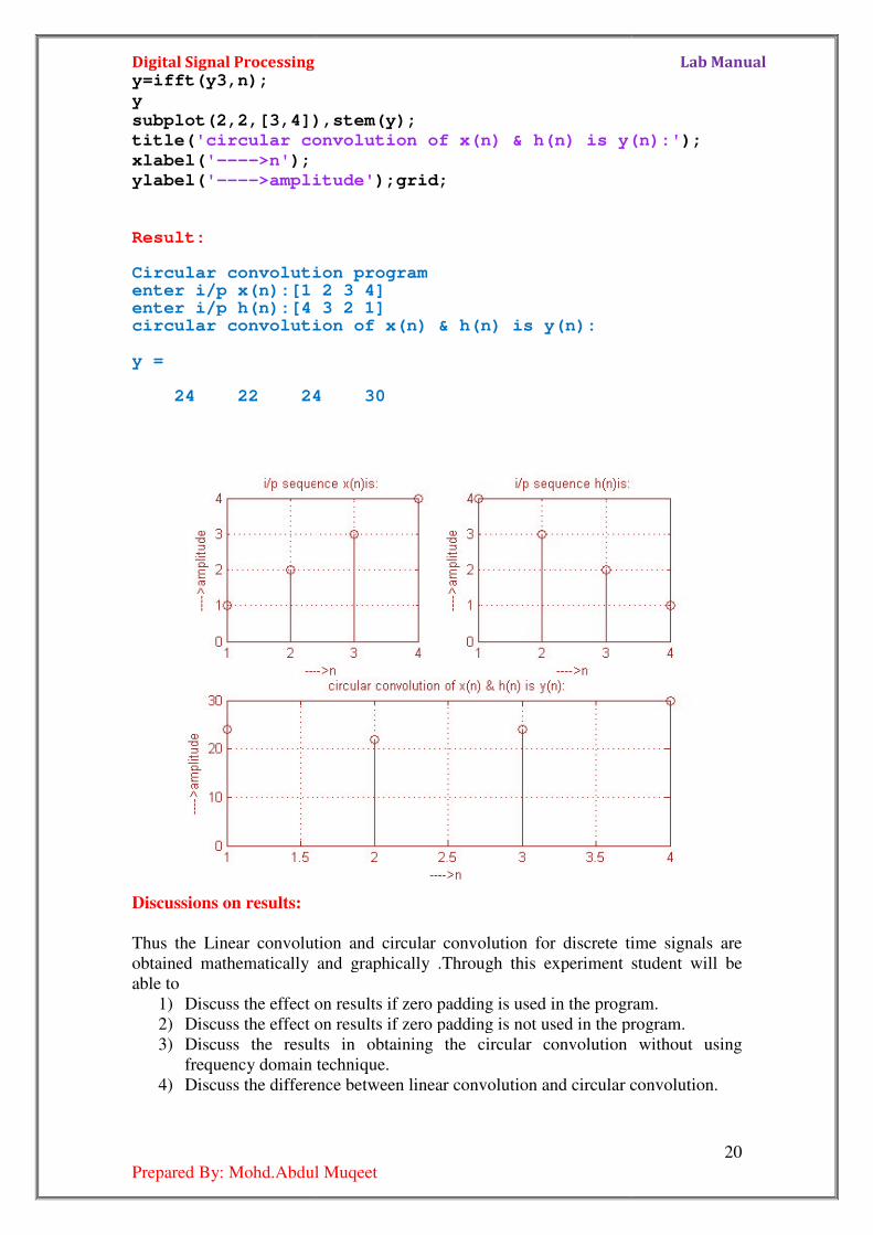
Program: clc;
clear all;
close all;
disp(‘Circular convolution program'
x=input('enter i/p x(n):'
m=length(x);
h=input('enter i/p h(n):'
n=length(h);
subplot(2,2,1), stem(x);
title('i/p sequence x(n)is:'
xlabel('---->n');
ylabel('---->amplitude'
subplot(2,2,2), stem(h);
title('i/p sequence h(n)is:'
xlabel('---->n');
ylabel('---->amplitude'
disp('circular convolution of x(n) & h(n) is y(n):'
y1=fft(x,n);
y2=fft(h,n);
y3=y1.*y2;
Prepared By: Mohd.Abdul Muqeet
‘Circular convolution program');
'enter i/p x(n):');
'enter i/p h(n):');
subplot(2,2,1), stem(x);
'i/p sequence x(n)is:');
>amplitude');grid;
subplot(2,2,2), stem(h);
'i/p sequence h(n)is:');
>amplitude');grid;
'circular convolution of x(n) & h(n) is y(n):'
Lab Manual
19
'circular convolution of x(n) & h(n) is y(n):');
Digital Signal Processing
Prepared By: Mohd.Abdul Muqeet
y=ifft(y3,n);
y
subplot(2,2,[3,4]),stem(y);
title('circular convolution of x(n) & h(n) is y(n):'
xlabel('---->n');
ylabel('---->amplitude'
Result: Circular convolution programenter i/p x(n):[1 2 3 4]enter i/p h(n):[4 3 2 1]circular convolution of x(n) & h(n) y = 24 22 24 30
Discussions on results:
Thus the Linear convolution and circular convolution for discrete time signals are
obtained mathematically and graphically .Through this experiment student will be
able to
1) Discuss the effect on results if zero padding is used in the program.
2) Discuss the effect on results if zero padding is not used in the program.
3) Discuss the results in obtaining the circular convolution without using
frequency domain technique.
4) Discuss the difference
Prepared By: Mohd.Abdul Muqeet
subplot(2,2,[3,4]),stem(y);
'circular convolution of x(n) & h(n) is y(n):'
>amplitude');grid;
Circular convolution program enter i/p x(n):[1 2 3 4] enter i/p h(n):[4 3 2 1] circular convolution of x(n) & h(n) is y(n):
24 22 24 30
Thus the Linear convolution and circular convolution for discrete time signals are
obtained mathematically and graphically .Through this experiment student will be
on results if zero padding is used in the program.
Discuss the effect on results if zero padding is not used in the program.
Discuss the results in obtaining the circular convolution without using
frequency domain technique.
Discuss the difference between linear convolution and circular convolution.
Lab Manual
20
'circular convolution of x(n) & h(n) is y(n):');
Thus the Linear convolution and circular convolution for discrete time signals are
obtained mathematically and graphically .Through this experiment student will be
on results if zero padding is used in the program.
Discuss the effect on results if zero padding is not used in the program.
Discuss the results in obtaining the circular convolution without using
between linear convolution and circular convolution.
Digital Signal Processing Lab Manual
21
Prepared By: Mohd.Abdul Muqeet
Experiment – 3 Aim: Write a Matlab program for computation of DFT and IDFT using Direct and
FFT method.
Apparatus: Matlab Software, PC
Theory:
DFT: Discrete Fourier Transform (DFT) is used for performing frequency analysis of
discrete time signals. DFT gives a discrete frequency domain representation whereas the
other transforms are continuous in frequency domain. The N point DFT of discrete time
signal x[n] is given by the equation
The inverse DFT allows us to recover the sequence x[n] from the frequency samples
FFT:
A fast Fourier transform (FFT) is an efficient algorithm to compute the discrete
Fourier transform (DFT) and its inverse. FFTs are of great importance to a wide variety of
applications, from digital signal processing and solving partial differential equations to
algorithms for quick multiplication of large integers. Evaluating the sums of DFT directly
would take O(N 2) arithmetical operations. An FFT is an algorithm to compute the same
result in only O(N log N) operations. In general, such algorithms depend upon the
factorization of N, but there are FFTs with O(N log N) complexity for all N, even for
prime N. Since the inverse DFT is the same as the DFT, but with the opposite sign in the
exponent and a 1/N factor, any FFT algorithm can easily be adapted for it as well.
Algorithm:
1) Get the input sequence
2) Find the DFT of the input sequence using direct equation of DFT.
3) Find the IDFT using the direct equation.
4) Find the FFT of the input sequence using MATLAB function.
5) Find the IFFT of the input sequence using MATLAB function.
4) Display the above outputs using stem function.
Program: %********** Direct DFT ***********
clc;close all;clear all;
xn=input('enter 8 inputs');
N=length(xn);
n=0:N-1;
k=0:N-1;
wn=exp((-1i*2*pi*n'*k)/N);
xf=wn*xn';
subplot(2,2,1); stem(abs(xf));
title('dft magnitude respone'); ylabel('magnitude');
xlabel('frequncy');

Digital Signal Processing
Prepared By: Mohd.Abdul Muqeet
% ******* Direct IDFT
WN=exp((1i*2*pi*n'*k)/N);
pn=WN*xf/N;
subplot(2,2,2);
stem(abs(pn));
title('idft magnitude respone'
ylabel('magnitude');xlabel('time');
%******* FFT Method
xp=fft(xn,N); subplot(2,2,3);
stem(abs(xp));
title('fft magnitude respone'
ylabel('magnitude');
xlabel('frequncy');
%******** IFFT methodxw=ifft(xp,N);
subplot(2,2,4);
stem(abs(xw));
title('ifft magnitude respone'
ylabel('magnitude');xlabel('time');
Results: enter 8 inputs[1 2 3 4 5 6 7 8]
Discussions on results: Thus from the results students will be able to
1. Discuss that the Fourier transform of a discrete time signal is also called as
Signal Spectrum.
2. Discuss the changes in the results due to more number of inputs in the given
sequences in finding the DFT and FFT.
3. Discuss that FFT performs faster and take less computational time compared
to DFT.
Prepared By: Mohd.Abdul Muqeet
IDFT **********
WN=exp((1i*2*pi*n'*k)/N);
'idft magnitude respone');
);
ethod**********
'fft magnitude respone');
);
);
method *********
'ifft magnitude respone');
);
enter 8 inputs[1 2 3 4 5 6 7 8]
Thus from the results students will be able to
Discuss that the Fourier transform of a discrete time signal is also called as
Discuss the changes in the results due to more number of inputs in the given
n finding the DFT and FFT.
Discuss that FFT performs faster and take less computational time compared
Lab Manual
22
Discuss that the Fourier transform of a discrete time signal is also called as
Discuss the changes in the results due to more number of inputs in the given
Discuss that FFT performs faster and take less computational time compared
Digital Signal Processing Lab Manual
23
Prepared By: Mohd.Abdul Muqeet
Experiment – 4
Aim: Write a Matlab program to verify Sampling Theorem
Apparatus: Matlab Software, PC
Theory:
Sampling Theorem: The sampling theorem, attributed to Nyquist, Shannon,
Kotelnikov and Whittaker, is useful when calculating the sampling frequency required
for use in the Analog-to-Digital converter.
The theorem states that a band limited signal can be reconstructed exactly if it is
sampled at a rate at least twice the maximum frequency component in it.
The maximum frequency component of g(t) is fm. To recover the signal g(t) exactly
from its samples it has to be sampled at a rate fs=2fm. The minimum required
sampling rate fs = 2fm is called Nyquist rate.
Sampling is also a process of converting a continuous time signal (analog signal) x(t)
into a d i scre t e t ime s ignal x [n] ,which i s r ep resent ed as a sequence
of numbers . (A/D Converter)
Converting back x[n] into analog (resulting in) x(t) is the process of
reconstruction.(D/A Converter)
Algorithm:
1) Input the desired frequency mf (for which sampling theorem is to be verified)
2) Generate the cosine wave, i.e a continuous-time signal given mathematically
as, ( ) cos(2 )mx t f tπ= where f represents the frequency and t the time.
3) Generate the discrete-time signals for Undersampling, Nyquist sampling
andoversampling conditions.
oversampled & under sampled conditions after sampling at instants n1, n2,
n3 which are given as, ,.
a. To do this for under sampling, choose sampling frequency
fs1<2*fm.For this sampling rate T1=1/fs1,
b. For Nyquist Sampling, choose sampling frequency fs2=2*fm.For
this sampling rate T2=1/fs2.
c. For Over Sampling, choose sampling frequency fs2>fd.
4) Plot the waveforms and hence prove sampling theorem.
Program:
clc;
clear all;
%define analog signal for comparison
t=-100:01:100;
fm=0.02;
x=cos(2*pi*t*fm);
subplot(2,2,1);
plot(t,x);
xlabel('time in sec');
ylabel('x(t)');
title('continuous time signal');
Digital Signal Processing Lab Manual
24
Prepared By: Mohd.Abdul Muqeet
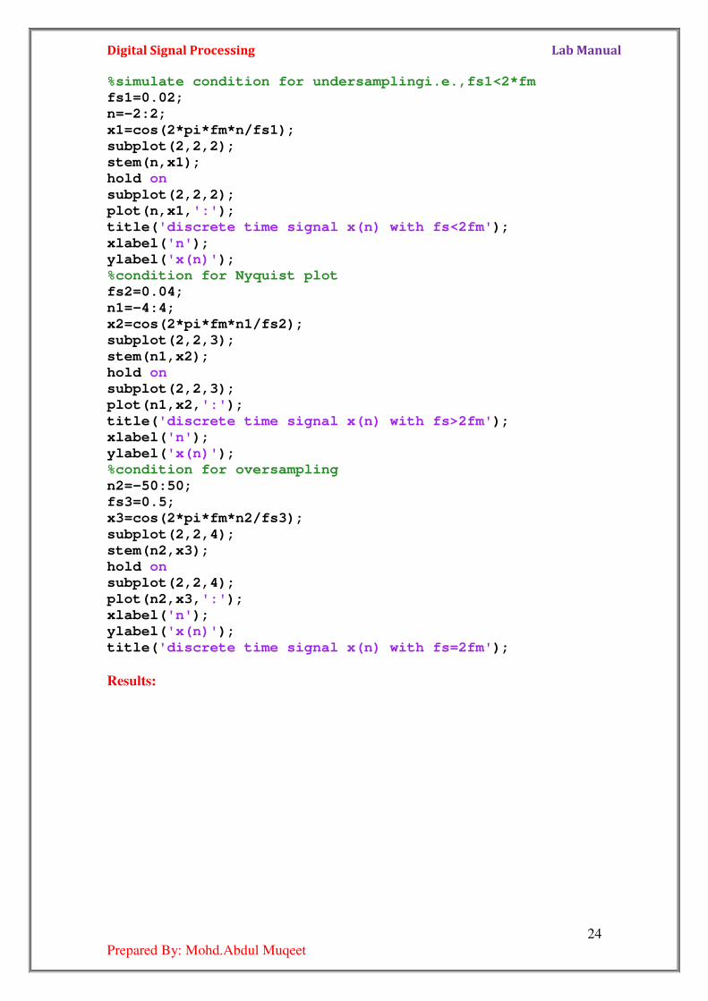
%simulate condition for undersamplingi.e.,fs1<2*fm
fs1=0.02;
n=-2:2;
x1=cos(2*pi*fm*n/fs1);
subplot(2,2,2);
stem(n,x1);
hold on
subplot(2,2,2);
plot(n,x1,':');
title('discrete time signal x(n) with fs<2fm');
xlabel('n');
ylabel('x(n)');
%condition for Nyquist plot
fs2=0.04;
n1=-4:4;
x2=cos(2*pi*fm*n1/fs2);
subplot(2,2,3);
stem(n1,x2);
hold on
subplot(2,2,3);
plot(n1,x2,':');
title('discrete time signal x(n) with fs>2fm');
xlabel('n');
ylabel('x(n)');
%condition for oversampling
n2=-50:50;
fs3=0.5;
x3=cos(2*pi*fm*n2/fs3);
subplot(2,2,4);
stem(n2,x3);
hold on
subplot(2,2,4);
plot(n2,x3,':');
xlabel('n');
ylabel('x(n)');
title('discrete time signal x(n) with fs=2fm');
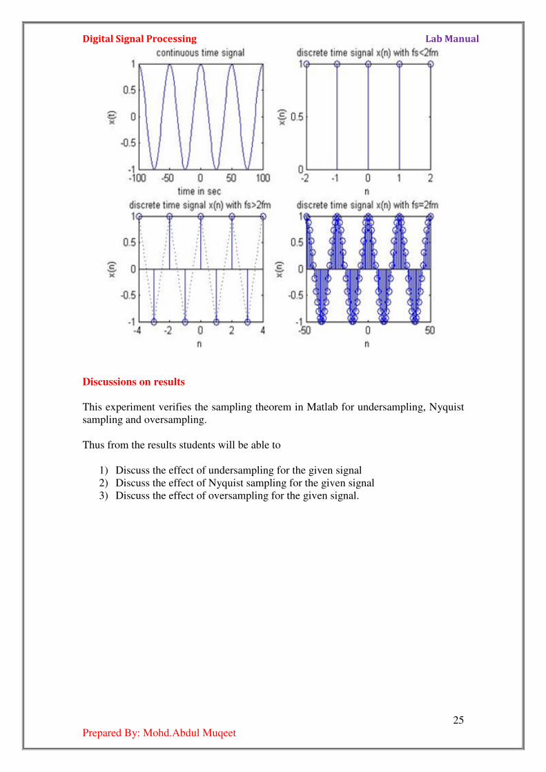
Results:
Digital Signal Processing Lab Manual
25
Prepared By: Mohd.Abdul Muqeet
Discussions on results
This experiment verifies the sampling theorem in Matlab for undersampling, Nyquist
sampling and oversampling.
Thus from the results students will be able to
1) Discuss the effect of undersampling for the given signal
2) Discuss the effect of Nyquist sampling for the given signal
3) Discuss the effect of oversampling for the given signal.
Digital Signal Processing Lab Manual
26
Prepared By: Mohd.Abdul Muqeet
Experiment – 5
Aim: -To Design and generate IIR Butterworth/ Chebyshev LP/HP Filter using
MATLAB
Apparatus Required: - MATLAB Software, PC
Theory: The Digital Filter Design problem involves the determination of a set of filter
coefficients to meet a set of design specifications. These specifications typically
consist of the width of the passband and the corresponding gain, the width of the
stopband(s) and the attenuation therein; the band edge frequencies (which give an
indication of the transition band) and the peak ripple tolerable in the passband and
stopband(s).
The design of IIR filters is closely related to the design of analog filters, which
is a widely studied topic. An analog filter is usually designed and a transformation is
carried out into the digital domain. Two transformations exist – the impulse invariant
transformation and the bilinear transformation.
Analog to Digital Domain Mapping Techniques Digital Filters are designed by using the values of both the past outputs and the
present input, an operation brought about by convolution. If such a filter is subjected
to an impulse then its output need not necessarily become zero. The impulse response
of such a filter can be infinite in duration. Such a filter is called an Infinite Impulse
Response filter or IIR filter. The infinite impulse response of such a filter implies the
ability of the filter to have an infinite impulse response. This indicates that the system
is prone to feedback and instability.
The experiment studies two different types of IIR filters Butterworth Filter, and
Chebyschev I type Filters.
IIR filters are designed essentially by the Impulse Invariance or the Bilinear
Transformation method.
1) Impulse Invariance This procedure involves choosing the response of the digital filter as an equi-
spaced sampled version of the analog filter.
1. Decide upon the desired frequency response
2. Design an appropriate analogue filter
3. Calculate the impulse response of this analogue filter
4. Sample the analogue filter's impulse response
5. Use the result as the filter coefficients
2) Bilinear Transformation:
The Bilinear Transformation method overcomes the effect of aliasing that is
caused to due the analog frequency response containing components at or beyond the
Nyquist Frequency. The bilinear transform is a method of compressing the infinite,
straight analogue frequency axis to a finite one long enough to wrap around the unit
circle once only. This is also sometimes called frequency warping. This introduces a
distortion in the frequency. This is undone by pre-warping the critical frequencies of
the analog filter (cut-off frequency, center frequency) such that when the analog filter
is transformed into the digital filter, the designed digital filter will meet the desired
specifications.
Digital Signal Processing Lab Manual
27
Prepared By: Mohd.Abdul Muqeet
Filter Types
Butterworth Filters Butterworth filters are causal in nature and of various orders, the lowest order
being the best (shortest) in the time domain, and the higher orders being better in the
frequency domain. Butterworth or maximally flat filters have a monotonic amplitude
frequency response which is maximally flat at zero frequency response and the
amplitude frequency response decreases logarithmically with increasing frequency.
A Butterworth filter is characterized by its magnitude frequency response,
1
22
1| ( ) |
1 ( ) N
c
H jΩ =
Ω+
Ω
Where N is the order of the filter and Ωc is defined as the cutoff frequency where the
filter magnitude is 1/√2 times the dc gain (Ω=0).
Chebyshev Filters Chebyshev filters are equiripple in either the passband or stopband. Hence the
magnitude response oscillates between the permitted minimum and maximum values
in the band a number of times depending upon the order of filters. There are two types
of chebyshev filters. The chebyshev I filter is equiripple in passband and monotonic in
the stopband, where as chebyshev II is just the opposite.
The Chebyshev low-pass filter has a magnitude response given by
( )1
2 2 2| | 1 ( )N
c
H j Tε
− Ω
Ω = + Ω
where є is a parameter related to the ripple present in the passband
TN(x) is given by
( )1
1
cos( cos ) | | 1,
cos( cosh ) | | 1,N
N x for x passbandC x
N x for x stopband
−
−
≤ =
≤
The magnitude response has equiripple pass band and maximally flat stop band. By
increasing the filter order N, the Chebyshev response approximates the ideal response.
The phase response of the Chebyshev filter is more non-linear than the Butter worth
filter for a given filter length N.
Algorithm:
1) Enter the pass band ripple (rp) and stop band ripple (rs).
2) Enter the pass band frequency (wp) and stop band frequency (ws).
3) Get the sampling frequency (fs).
4) Calculate normalized pass band frequency, and normalized stop band frequency w1
and w2 respectively.
w1 = 2 * wp /fs
w2 = 2 * ws /fs
5) Make use of the following function to calculate order of filter
Butterworth filter order
[n,wn]=buttord(w1,w2,rp,rs)
Digital Signal Processing Lab Manual
28
Prepared By: Mohd.Abdul Muqeet
Chebyshev filter order
[n,wn]=cheb1ord(w1,w2,rp,rs)
6) Design an nth order digital lowpass Butterworth or Chebyshev filter using the
following statements.
Butterworth filter
[b, a]=butter (n, wn)
Chebyshev filter
[b,a]=cheby1(n,0.5,wn)
OR Design an nth order digital high pass Butterworth or Chebyshev filter using the
following statement.
Butterworth filter
[b,a]=butter (n, wn,’high’)
Chebyshev filter
[b,a]=cheby1 (n, 0.5, wn,'high')
7) Find the digital frequency response of the filter by using ‘freqz( )’ function
[H,w]=freqz(b,a,512,fs)
8) Calculate the magnitude of the frequency response in decibels (dB)
mag=20*log10 (abs (H))
9) Plot the magnitude response [magnitude in dB Vs normalized frequency (Hz]]
10) Calculate the phase response using an = angle (H)
11) Plot the phase response [phase in radians Vs normalized frequency (Hz)].
Program:
% IIR filters
clc; clear all; close all;
warning off;
disp('enter the IIR filter design specifications');
rp=input('enter the passband ripple');
rs=input('enter the stopband ripple');
wp=input('enter the passband freq');
ws=input('enter the stopband freq');
fs=input('enter the sampling freq');
w1=2*wp/fs;%normalized pass band frequency
w2=2*ws/fs;%normalized stop band frequency
[n,wn]=buttord(w1,w2,rp,rs);% Find the order n and cut-
off frequency
ch=input('give type of filter 1:LPF,2:HPF');
switch ch
case 1
disp('Frequency response of Butterworth IIR LPF is:');
[b,a]=butter(n,wn); % Find the filter coefficient of LPF
[H,w]=freqz(b,a,512,fs);% to get the transfer function
of the filter
mag=20*log10(abs(H));
phase=angle(H);
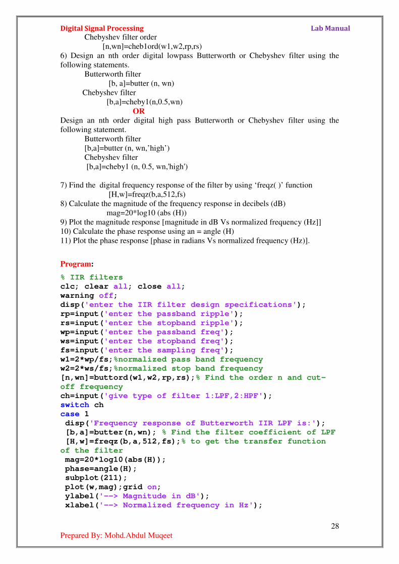
subplot(211);
plot(w,mag);grid on;
ylabel('--> Magnitude in dB');
xlabel('--> Normalized frequency in Hz');
Digital Signal Processing Lab Manual
29
Prepared By: Mohd.Abdul Muqeet
title('Magnitude Response of the desired Butterworh
LPF');
subplot(212);
plot(w,phase);grid on;
ylabel('--> Phase in radians');
xlabel('--> Normalized frequency in Hz');
title('Phase Response of the desired Butterworh LPF');
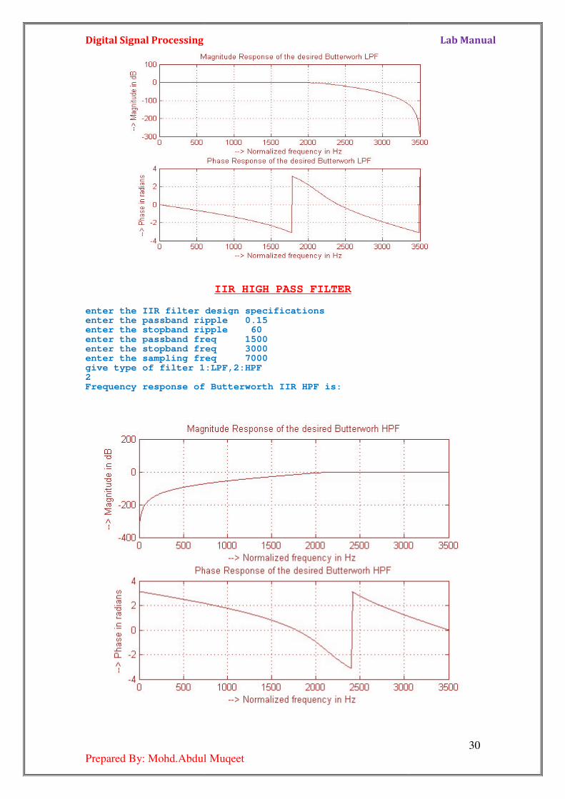
case 2
disp('Frequency response of IIR Butterworth HPF is:');
[b,a]=butter(n,wn,'high'); % Find the filter co-
efficients of HPF
[H,w]=freqz(b,a,512,fs);% to get the transfer function
of the filter
mag=20*log10(abs(H));
phase=angle(H);
subplot(211);
plot(w,mag);grid on;
ylabel('--> Magnitude in dB');
xlabel('--> Normalized frequency in Hz');
title('Magnitude Response of the desired Butterworh
HPF');
subplot(212);
plot(w,phase);grid on;
ylabel('--> Phase in radians');
xlabel('--> Normalized frequency in Hz');
title('Phase Response of the desired Butterworh HPF');
end
Results:
enter the IIR filter design specifications enter the passband ripple 0.15 enter the stopband ripple 60 enter the passband freq 1500 enter the stopband freq 3000 enter the sampling freq 7000 give type of filter 1:LPF,2:HPF 1 Frequency response of Butterworth IIR LPF is:
Digital Signal Processing
Prepared By: Mohd.Abdul Muqeet
enter the IIR filter design specificationsenter the passband ripple 0.15enter the stopband ripple 60enter the passband freq 1500enter the stopband freq 3000enter the sampling freq 7000give type of filter 1:LPF,2:HPF2 Frequency response of Butterworth IIR HPF is
Prepared By: Mohd.Abdul Muqeet
IIR HIGH PASS FILTER
enter the IIR filter design specifications enter the passband ripple 0.15 enter the stopband ripple 60 enter the passband freq 1500 enter the stopband freq 3000 enter the sampling freq 7000 give type of filter 1:LPF,2:HPF
Frequency response of Butterworth IIR HPF is:
Lab Manual
30

Digital Signal Processing Lab Manual
31
Prepared By: Mohd.Abdul Muqeet
%To design a Chebyshev (Type-I) Low/High Pass Filter for the
given specifications
clc; clear all; close all;
disp('enter the IIR filter design specifications');
rp=input('enter the passband ripple');
rs=input('enter the stopband ripple'); wp=input('enter the passband freq');
ws=input('enter the stopband freq');
fs=input('enter the sampling freq');
w1=2*wp/fs;%to get normalized pass band frequency
w2=2*ws/fs;% to get normalized stop band frequency
ch=input('give type of filter 1:LPF,2:HPF');
% to get the order and cut-off frequency of the filter
[n,wn]=cheb1ord(w1,w2,rp,rs);
switch ch
case 1
disp('Frequency response of Chebyshev IIR LPF is:');
[b,a]=cheby1(n,0.5,wn);% to get the filter coefficients
% to get the transfer function of the filter
[H,w]=freqz(b,a,512,fs);
mag=20*log10(abs(H)); phase=angle(H);
subplot(211);
plot(w,mag);grid on;
ylabel('--> Magnitude in dB');
xlabel('--> Normalized frequency in Hz');
title('Magnitude Response of the desired Chebyshev Type -I)
LPF'); subplot(212);
plot(w,phase);grid on;
ylabel('--> Phase in radians');
xlabel('--> Normalized frequency in Hz');
title('Phase Response of the desired Chebyshev(Type-I)LPF');
case 2 disp('Frequency response of Chebyshev IIR HPF is:');
% to get the filter coefficients
[b,a]=cheby1(n,0.5,wn,'high');
% to get the transfer function of the filter
[H,w]=freqz(b,a,512,fs);
mag=20*log10(abs(H)); phase=angle(H);
subplot(211);
plot(w,mag);grid on;
ylabel('--> Magnitude in dB');
xlabel('--> Normalized frequency in Hz');
title('Magnitude Response of the desired Chebyshev(Type-
I)HPF'); subplot(212);
plot(w,phase);grid on;
ylabel('--> Phase in radians');
xlabel('--> Normalized frequency in Hz');
title('Phase Response of the desired Chebyshev(Type-I)HPF'); end

Digital Signal Processing
Prepared By: Mohd.Abdul Muqeet
Results:
enter the IIR filter design specifications
enter the passband ripple
enter the stopband ripple
enter the passband freq
enter the stopband freq
enter the sampling freq
give type of filter 1:LPF,2:HPF
1
Frequency response of Chebyshev IIR LPF is:
Result:
enter the IIR filter design
enter the passband ripple
enter the stopband ripple
enter the passband freq
enter the stopband freq
enter the sampling freq
give type of filter 1:LPF,2:HPF
2
Frequency response of Chebyshev IIR HPF is:
Prepared By: Mohd.Abdul Muqeet
enter the IIR filter design specifications
enter the passband ripple 0.15
enter the stopband ripple 60
enter the passband freq 1500
enter the stopband freq 3000
enter the sampling freq 7000
give type of filter 1:LPF,2:HPF
Frequency response of Chebyshev IIR LPF is:
High Pass Filter
enter the IIR filter design specifications
enter the passband ripple 0.15
enter the stopband ripple 60
enter the passband freq 1500
enter the stopband freq 3000
enter the sampling freq 7000
give type of filter 1:LPF,2:HPF
Frequency response of Chebyshev IIR HPF is:
Lab Manual
32

Digital Signal Processing
Prepared By: Mohd.Abdul Muqeet
Discussions on results:
By this experiment we have studied the LP/HP IIR digital filter designing.
From the obtained results the students will be able to
1) Discuss the effect of order of the filer on magnitude response.
2) Discuss the effect of variation in
frequency, stop band frequency and sa
designing the IIR Butterworth digital filter.
3) Discuss the effect of variation in
frequency, stop band frequency and sa
designing the IIR Chebyshev digital filter.
Prepared By: Mohd.Abdul Muqeet
By this experiment we have studied the LP/HP IIR digital filter designing.
From the obtained results the students will be able to
Discuss the effect of order of the filer on magnitude response.
Discuss the effect of variation in pass band ripple, stop band ripple, pass band
frequency, stop band frequency and sampling frequency respectively in
designing the IIR Butterworth digital filter.
Discuss the effect of variation in pass band ripple, stop band ripple, pass band
frequency, stop band frequency and sampling frequency respectively in
designing the IIR Chebyshev digital filter.
Lab Manual
33
By this experiment we have studied the LP/HP IIR digital filter designing.
pass band ripple, stop band ripple, pass band
mpling frequency respectively in
and ripple, pass band
mpling frequency respectively in
Digital Signal Processing Lab Manual
34
Prepared By: Mohd.Abdul Muqeet
Experiment – 6
Aim: - Design and implementation of FIR Filter (LP/HP) to meet given specifications
Using Windowing technique
a. Rectangular window
b. Hamming window
c. Kaiser window
Apparatus: Matlab Software, PC
Theory: A linear-phase is required throughout the passband of the filter to preserve the
shape of the given signal in the passband. A causal IIR filter cannot give linear-phase
characteristics and only special types of FIR filters that exhibit center symmetry in its
impulse response give the linear-space. A Finite Impulse Response (FIR) filter is a
discrete linear time-invariant system whose output is based on the weighted
summation of a finite number of past inputs.
A zero-phase frequency response of an ideal filter is given as
1, ,( )
0, .
cj
LP
c
H e ωω ω
ω ω π
≤=
< ≤
Hence time domain impulse response is
( )sin( )1
[ ] ..2
j j k cd d
c
kh k H e e d
k
πω ω
π
ωω α
π ω−
= = =∫
so the impulse response is doubly infinite, not absolutely summable, and therefore
unrealizable.
By setting all impulse response coefficient outside the range
equal to zero, we arrival at a finite-length noncausal approximation of length
which when shifted to the right yield the coefficients of a causal FIR lowpass filter:
Gibbs phenomenon
The causal FIR filter obtained by simply truncating the impulse response coefficients
of the ideal filters exhibit an oscillatory behavior in their respective magnitude
responses which is more commonly referred to as the Gibbs phenomenon
Cause of Gibbs phenomenon:
The FIR filter obtained by truncation can be expressed as
( )1( ) ( ) ( )
2
j j j
dH e H e e dπ
ω φ ω φ
πψ φ
π−
−= ∫
The window used to achieve simple truncation of the ideal filter is rectangular
window
M n M− ≤ ≤
2 1N M= +
[ ]sin( ( ))
( ) ,0 1
0,
c
LP
n M
n Mh n n N
otherwise
ω
π
−
−= ≤ ≤ −
[ ] [ ] [ ]dh n h n nω= ⋅
1,0[ ]
0,R
n Mw n
otherwise
≤ ≤=
Digital Signal Processing Lab Manual
35
Prepared By: Mohd.Abdul Muqeet
Thus by applying windowing functions we can obtain FIR filters.
Available Fixed window functions Rectangular, Bartlett, Hamming, Hanning,
Blackmann etc.
Hamming window function
In Adjustable Window Functions, windows have been developed that provide control
over ripple by means of an additional parameter.
Like Kaiser Window
Where β is an adjustable parameter and 0 ( )I β is a zero order Bessel function
To design a FIR filter order of the filter should be specified or can be calculated from
the following equation
( )( )
1020 log 13
14.6 2
p s
s p
r rN
w w π
− −=
−
rp=passband ripple, rs=stopband ripple, wp=passband frequency
ws=stopband frequency
Then from order of the filter we can find the length by which a window function can
be applied.
Algorithm:
FIR Low Pass Filter design
1) Enter the pass band ripple (rp) and stop band ripple (rs).
2) Enter the pass band frequency (wp) and stop band frequency (ws).
3) Get the sampling frequency (fs), beta value for Kaiser window.
4) Calculate the analog pass band edge frequencies, w1 and w2.
i. w1 = 2*wp/fs
ii. w2 = 2*ws/fs
5) Calculate the order of the filter using the order equation.
6) Use switch condition and ask the user to choose either Rectangular Window or
Hamming window or Kaiser window.
7) Use rectwin, hamming, Kaiser Commands
Command fir1 uses the window method of FIR filter design, If w(n) denotes a
window, where 1 ≤ n ≤ N, and the impulse response of the ideal filter is h(n),
where hd(n) is the inverse Fourier transform of the ideal frequency response.
8) Calculate the digital frequency response using the command ‘freqz()’
9) Calculate the magnitude of the frequency response in decibels
m=20*log10 (abs(h))
10) Plot the magnitude response [magnitude in dB Vs normalized frequency
(om/pi)]
2[ ] 0.54 0.46cos( ),
2 1
nw n M n M
M
π= + − ≤ ≤
+
( ) ( )
2
0
0
1 /
[ ] ,
I n M
w n M n MI
β
β
−
= − ≤ ≤
[ ] [ ] [ ]dh n h n nω= ⋅
Digital Signal Processing Lab Manual
36
Prepared By: Mohd.Abdul Muqeet
Program:
%FIR Low Pass/High pass filter design using
Rectangular/Hamming/Kaiser window
clc; clear all; close all; rp=input('enter passband ripple');
rs=input('enter the stopband ripple');
wp=input('enter passband freq');
ws=input('enter stopband freq');
fs=input('enter sampling freq ');
beta=input('enter beta value'); w1=2*wp/fs;
w2=2*ws/fs;
num=-20*log10(sqrt(rp*rs))-13;
dem=14.6*(ws-wp)/fs;
n=ceil(num/dem);
n1=n+1; if(rem(n,2)~=0)
n1=n; n=n-1;
end
c=input('enter your choice of window function 1. rectangular
2. Hamming 3.kaiser: \n ');
if(c==1)
y=rectwin(n1); disp('Rectangular window filter response');
end
if (c==2)
y=hamming(n1);
disp('Hamming window filter response');
end if(c==3)
y=kaiser(n1,beta);
disp('kaiser window filter response');
end
ch=input('give type of filter 1:LPF,2:HPF'); switch ch
case 1
b=fir1(n,w1,y);
[h,o]=freqz(b,1,256);
m=20*log10(abs(h));
plot(o/pi,m);
title('LPF'); xlabel('(a) Normalized frequency-->');
ylabel('Gain in dB-->');
case 2
b=fir1(n,w1,'high',y);
[h,o]=freqz(b,1,256); m=20*log10(abs(h));
plot(o/pi,m);
title('HPF');
xlabel('(b) Normalized frequency-->');
ylabel('Gain in dB-->');
end
Digital Signal Processing
Prepared By: Mohd.Abdul Muqeet
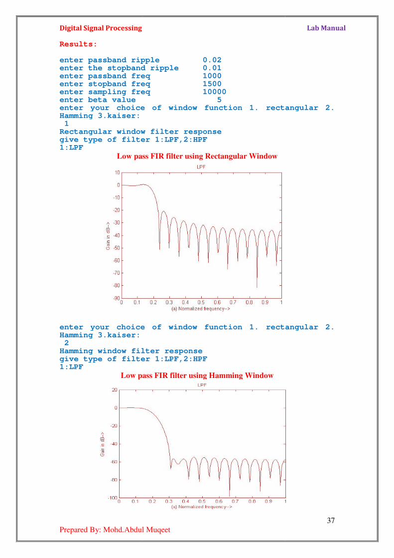
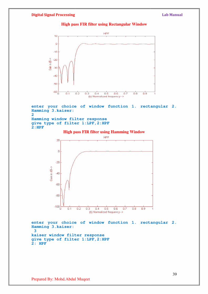
Results: enter passband ripple 0.02enter the stopband ripple enter passband freq 1000enter stopband freq 1500enter sampling freq 10000enter beta value 5enter your choice of window function 1. rectangular 2. Hamming 3.kaiser: 1 Rectangular window filter responsegive type of filter 1:LPF,2:HPF1:LPF
Low pass FIR fi
enter your choice of window function 1. rectangular 2. Hamming 3.kaiser: 2 Hamming window filter responsegive type of filter 1:LPF,2:HPF1:LPF
Low pass FIR filter using Hamming
Prepared By: Mohd.Abdul Muqeet
enter passband ripple 0.02 enter the stopband ripple 0.01 enter passband freq 1000
freq 1500 enter sampling freq 10000 enter beta value 5 enter your choice of window function 1. rectangular 2. Hamming 3.kaiser:
Rectangular window filter response give type of filter 1:LPF,2:HPF
Low pass FIR filter using Rectangular Window
enter your choice of window function 1. rectangular 2. Hamming 3.kaiser:
Hamming window filter response give type of filter 1:LPF,2:HPF
ass FIR filter using Hamming Window
Lab Manual
37
enter your choice of window function 1. rectangular 2.
enter your choice of window function 1. rectangular 2.
Digital Signal Processing
Prepared By: Mohd.Abdul Muqeet
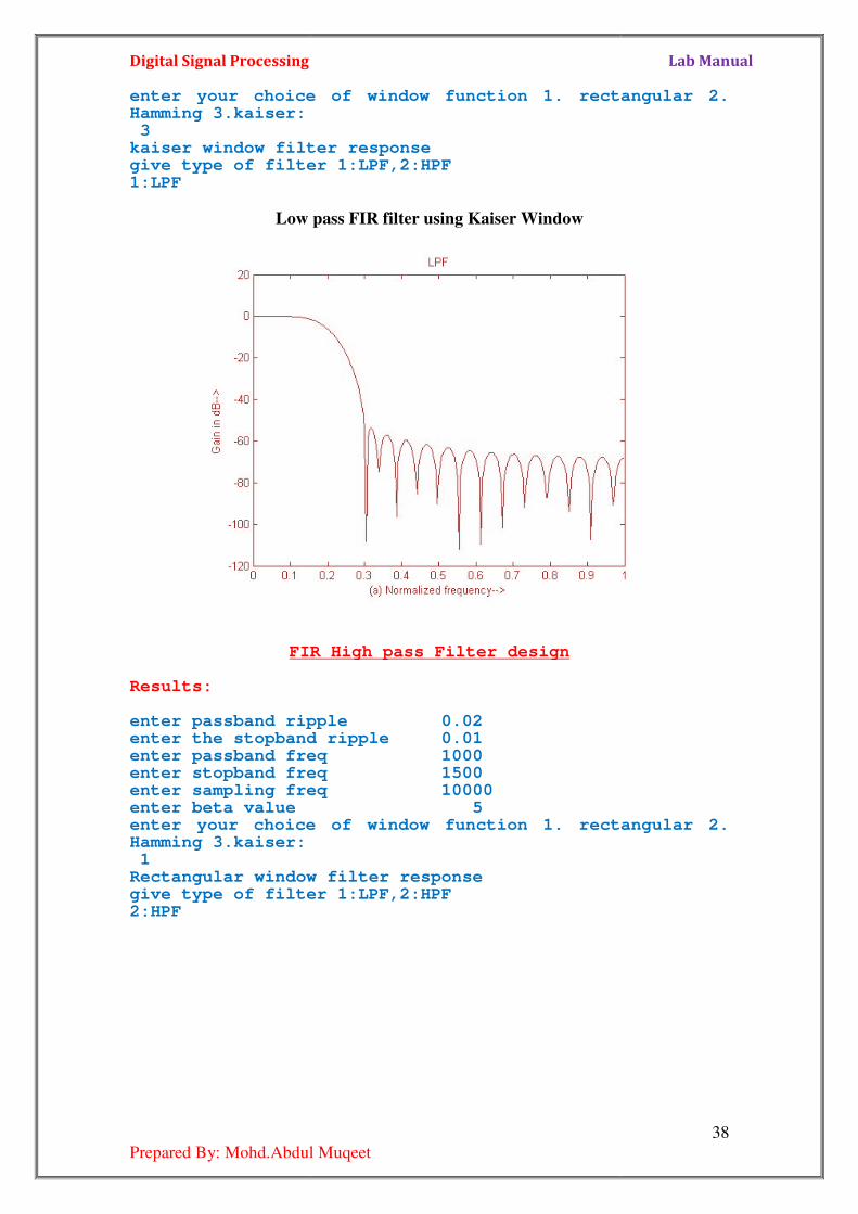
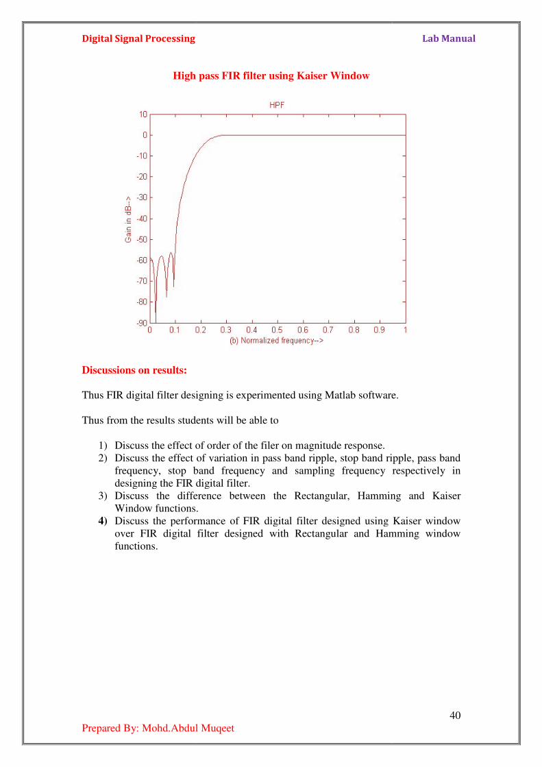
enter your choice of window function 1. rectangular 2. Hamming 3.kaiser: 3 kaiser window filter responsegive type of filter 1:LPF,2:HPF1:LPF
Low pass FIR filter using
FIR High pass Filter design Results: enter passband ripple enter the stopband ripple enter passband freq 1000enter stopband freq 1500enter sampling freq 10000enter beta value 5enter your choice of window function 1. rectangular 2. Hamming 3.kaiser: 1 Rectangular window filter responsegive type of filter 1:LPF,2:HPF2:HPF
Prepared By: Mohd.Abdul Muqeet
enter your choice of window function 1. rectangular 2. Hamming 3.kaiser:
kaiser window filter response give type of filter 1:LPF,2:HPF
Low pass FIR filter using Kaiser Window
FIR High pass Filter design
enter passband ripple 0.02 enter the stopband ripple 0.01 enter passband freq 1000 enter stopband freq 1500 enter sampling freq 10000 enter beta value 5 enter your choice of window function 1. rectangular 2. Hamming 3.kaiser:
Rectangular window filter response give type of filter 1:LPF,2:HPF
Lab Manual
38
enter your choice of window function 1. rectangular 2.
enter your choice of window function 1. rectangular 2.
Digital Signal Processing
Prepared By: Mohd.Abdul Muqeet
High pass FIR filter using Rectangular Window
enter your choice of window function 1. rectangular 2. Hamming 3.kaiser: 2 Hamming window filter responsegive type of filter 1:LPF,2:HPF2:HPF
High pass FIR filter using
enter your choice of window function 1. rectangular 2.Hamming 3.kaiser: 3 kaiser window filter responsegive type of filter 1:LPF,2:HPF2: HPF
Prepared By: Mohd.Abdul Muqeet
pass FIR filter using Rectangular Window
enter your choice of window function 1. rectangular 2. Hamming 3.kaiser:
Hamming window filter response give type of filter 1:LPF,2:HPF
pass FIR filter using Hamming Window
enter your choice of window function 1. rectangular 2.Hamming 3.kaiser:
kaiser window filter response give type of filter 1:LPF,2:HPF
Lab Manual
39
enter your choice of window function 1. rectangular 2.
enter your choice of window function 1. rectangular 2.
Digital Signal Processing
Prepared By: Mohd.Abdul Muqeet
High
Discussions on results:
Thus FIR digital filter designing is experimented using Matlab software.
Thus from the results students will be able to
1) Discuss the effect of order of the filer on
2) Discuss the effect of variation in
frequency, stop band frequency and sa
designing the FIR digital filter.
3) Discuss the difference between the Rectangular, Hamming and Kaiser
Window functions.
4) Discuss the performance of FIR digital filter designed using Kaiser window
over FIR digital filter designed with Rectangular and
functions.
Prepared By: Mohd.Abdul Muqeet
pass FIR filter using Kaiser Window
filter designing is experimented using Matlab software.
results students will be able to
Discuss the effect of order of the filer on magnitude response.
Discuss the effect of variation in pass band ripple, stop band ripple, pass band
frequency, stop band frequency and sampling frequency respectiv
designing the FIR digital filter.
Discuss the difference between the Rectangular, Hamming and Kaiser
Window functions.
Discuss the performance of FIR digital filter designed using Kaiser window
over FIR digital filter designed with Rectangular and Hamming window
Lab Manual
40
filter designing is experimented using Matlab software.
pass band ripple, stop band ripple, pass band
mpling frequency respectively in
Discuss the difference between the Rectangular, Hamming and Kaiser
Discuss the performance of FIR digital filter designed using Kaiser window
Hamming window

Digital Signal Processing Lab Manual
41
Prepared By: Mohd.Abdul Muqeet
Cycle-II
Digital Signal Processing Lab Manual
42
Prepared By: Mohd.Abdul Muqeet
TMS320C50 Architecture Overview
1. Introduction: It is needless to say that in order to utilize the full feature of the DSP chip
TMS320C50, the DSP engineer must have a complete knowledge of the DSP device.
This chapter is an introduction to the hardware aspects of the TMS320C50. The
important units of TMS320C50 are discussed.
2. The DSP Chip TMS320C50: The TMS320C50 is a 16-bit fixed point digital signal processor that combines
the flexibility of a high speed controller with the numerical capability of an array
processor, thereby offering an inexpensive alternative to multichip bit-slice
processors. The highly paralleled architecture and efficient instruction set provide
speed and flexibility capable of executing 10 MIPS (Million Instructions per Second).
The TMS320C50 optimizes speed by implementing functions in hardware that other
processors implement through microcode or software. This hardware intensive
approach provides the design engineer with processing power previously unavailable
on a single chip.
The TMS320C50 is the third generation digit l signal processor in the
TMS320 family. Its powerful instruction set, inherent flexibility, high-speed number-
crunching capabilities, and innovative architecture have made this high-performance,
cost-effective processor the ideal solution to many telecommunications, computer,
commercial, industrial, and military applications.
3. Key Features of TMS320C50: The key features of the Digital Signal Processor TMS320C50 are:
* 35-/50-ns single-cycle fixed-point instruction execution time (28.6/20 MIPS)
* Upward source-code compatible with all `C1X and `C2x devices
* RAM-based memory operation (`C50)
* 9K x 16-bit single-cycle on-chip program/data RAM (`C50)
* 2K x 16-bit single-cycle on-chip boot ROM (`C50)
* 1056 x 16-bit dual-access on-chip data RAM
* 224K x 16-bit maximum addressable external memory space (64K program, 64K
data, 64K I/O, and 32K global)
* 32-bit arithmetic logic unit (ALU), 32-bit accumulator (ACC), and 32-bit
accumulator buffer (ACCB)
* 16-bit parallel logic unit (PLU)
* 16 x 16-bit parallel multiplier with a 32-bit product capability.
* Single-cycle multiply/accumulate instructions
* Eight auxiliary registers with a dedicated auxiliary register arithmetic unit for
indirect addressing.
* Eleven context-switch registers (shadow registers) for storing strategic CPU
controlled registers during an interrupt service routine
* Eight-level hardware stack
* 0- to 16-bit left and right data barrel-shifters and a 64-bit incremental data shifter
* Two indirectly addressed circular buffers for circular addressing
* Single-instruction repeat and block repeat operations for program code
* Block memory move instructions for better program/data management
* Full-duplex synchronous serial port for direct communication between the `C5x and
another serial device
* Time-division multiple-access (TDM) serial port
Digital Signal Processing
Prepared By: Mohd.Abdul Muqeet
* Interval timer with period, control, and counter registers for software
reset
* 64K parallel I/O ports, 16 of which are memory mapped
* Sixteen software programmable wait
memory spaces.
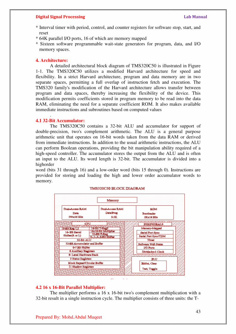
4. Architecture: A detailed architectural block diagram of TMS320C50 is
1-1. The TMS320C50 utilizes a modified Harvard architecture for speed and
flexibility. In a strict Harvard architecture, program and data memory are in two
separate spaces, permitting a full
TMS320 family's modification of the Harvard
program and data spaces, thereby increasing the flexibility
modification permits coefficients stored in program memory to be read into
RAM, eliminating the need for a separate coefficient ROM. It also makes available
immediate instructions and subroutines based on computed values
.
4.1 32-Bit Accumulator: The TMS320C50 contains a 32
double-precision, two's complement arithmetic. The ALU is a general purpose
arithmetic unit that operates on 16
from immediate instructions. In addition to the usual
can perform Boolean operations, pro
high-speed controller. The accumulator stores the output from the ALU and
an input to the ALU. Its word length is 32
highorder
word (bits 31 through 16) and a
provided for storing and loading the high and lower order accumulator words to
memory.
4.2 16 x 16-Bit Parallel MultiplierThe multiplier performs a 16 x 16
32-bit result in a single instruction cycle. The multiplier consists of three units: the T
Prepared By: Mohd.Abdul Muqeet
* Interval timer with period, control, and counter registers for software
* 64K parallel I/O ports, 16 of which are memory mapped
* Sixteen software programmable wait-state generators for program, data, and I/O
A detailed architectural block diagram of TMS320C50 is illustrated in Figure
TMS320C50 utilizes a modified Harvard architecture for speed and
Harvard architecture, program and data memory are in two
separate spaces, permitting a full overlap of instruction fetch and execution.
TMS320 family's modification of the Harvard architecture allows transfer between
program and data spaces, thereby increasing the flexibility of the device. This
modification permits coefficients stored in program memory to be read into
liminating the need for a separate coefficient ROM. It also makes available
immediate instructions and subroutines based on computed values
The TMS320C50 contains a 32-bit ALU and accumulator for support of
complement arithmetic. The ALU is a general purpose
arithmetic unit that operates on 16-bit words taken from the data RAM or derived
from immediate instructions. In addition to the usual arithmetic instructions, the ALU
can perform Boolean operations, providing the bit manipulation ability required of a
speed controller. The accumulator stores the output from the ALU and
an input to the ALU. Its word length is 32-bit. The accumulator is divided into a
word (bits 31 through 16) and a low-order word (bits 15 through 0). Instructions are
provided for storing and loading the high and lower order accumulator words to
Bit Parallel Multiplier: The multiplier performs a 16 x 16-bit two's complement multiplication with
a single instruction cycle. The multiplier consists of three units: the T
Lab Manual
43
* Interval timer with period, control, and counter registers for software stop, start, and
state generators for program, data, and I/O
illustrated in Figure
TMS320C50 utilizes a modified Harvard architecture for speed and
Harvard architecture, program and data memory are in two
overlap of instruction fetch and execution. The
architecture allows transfer between
of the device. This
modification permits coefficients stored in program memory to be read into the data
liminating the need for a separate coefficient ROM. It also makes available
bit ALU and accumulator for support of
complement arithmetic. The ALU is a general purpose
words taken from the data RAM or derived
arithmetic instructions, the ALU
ability required of a
speed controller. The accumulator stores the output from the ALU and is often
bit. The accumulator is divided into a
order word (bits 15 through 0). Instructions are
provided for storing and loading the high and lower order accumulator words to
bit two's complement multiplication with a
a single instruction cycle. The multiplier consists of three units: the T-
Digital Signal Processing Lab Manual
44
Prepared By: Mohd.Abdul Muqeet
Register, P-Register, and multiplier array. The 16-bit T-Register temporarily
stores the multiplicand and the P-Register stores the 32-bit product. Multiplier values
either
come from the data memory or are derived immediately from the MPY (multiply
immediate) instruction word. The fast on-chip multiplier allows the device to perform
fundamental operations such as convolution, correlation, and filtering. Two
multiply/accumulate instructions in the instruction set fully utilize the computational
bandwidth of the multiplier, allowing both operands to be processed simultaneously.
4.3 Shifters: A 16-bit scaling shifter is available at the accumulator input. This shifter
produces a left shift of 0 to 16-bits on the input data to accumulator.
TMS320C50 also contains a shifter at the accumulator output. This shifter provides a
left shift of 0 to 7, on the data from either the ACCH or ACCL register, right, before
transferring the product to accumulator.
4.4 Date and Program Memory: Since the TMS320C50 uses Harvard architecture, data and program memory
reside in two separate spaces. Additionally TMS320C50 has one more memory space
called I/O memory space. The total memory capacity of TMS320C50 is 64KW each
of Program, Data and I/O memory. The 64KW of data memory is divided into 512
pages with each page containing 128 words. Only one page can be active at a time.
One data page selection is done by setting data page pointer. TMS320C50 has 1056
words of dual access on chip data RAM and 9K words of single access Data/Program
RAM. The 1056 words of on chip data memory is divided as three blocks B0, B1 &
B2, of which B0 can be configured as program or data RAM.
Out of the 64KW of total program memory, TMS320C50 has 2K words of on-chip
program ROM.
The TMS320C50 offers two modes of operation defined by the state of the
MC/MP pin: the microcomputer mode (MC/MP = 1) or the microprocessor mode
(MC/MP = 0). In the microcomputer mode, on-chip ROM is mapped into the memory
space with upto 2K words of memory available. In the microprocessor mode all 64K
words of program memory are external.
4.5 Interrupts and Subroutines: The TMS320C50 has three external maskable user interrupts available for
external devices that interrupt the processor.
The TMS320C50 contains an eight-level hardware stack for saving the contents of the
program counter during interrupts and subroutine calls. Instructions are available for
saving the device's complete context. PUSH and POP instructions permit a level of
nesting restricted only by the amount of available RAM.
4.6 Serial Port: A full-duplex on-chip serial port provides direct communication with serial
devices such as codecs, serial A/D converters and other serial systems. The interface
signals are compatible with codecs and many others serial devices with a minimum of
external hardware.
4.7 Input and Output:
Digital Signal Processing Lab Manual
45
Prepared By: Mohd.Abdul Muqeet
The 16-bit parallel data bus can be utilised to perform I/O functions in two
cycles. The I/O ports are addressed by the four LSBs on the address lines, allowing 16
input and 16 output ports. In addition, polling input for bit test and jump operations
(BIO) and three interrupt pins (INT0 - INT2) have been incorporated for multitasking.
Software Overview
This chapter illustrates the use of program and execution mainly in the standalone
mode.
The Micro-50 EB has 3 software development tools namely
1. Standalone Mode
2. Monitor program
3. Serial Mode
In "Standalone Mode" the Micro-50 EB works with a 104 keys keyboard and
16x2 LCD display and line assembler. With this configuration, the student can enter
his program through the keyboard and edit and display it on the LCD display. The
user can enter the Mnemonics using the Line Assembler, and debug the program to
run it on Micro-50 EB.
"Monitor Program" is used to enter data directly into Data or Program memory,
display the data etc. It has several commands to enter the user program, for editing
and debugging.
In "Serial Mode", it works with a IBM PC computer and program entry and
debugging is done at the PC level. The Chapter-6 gives details about this operation.
Program and Execution:
1. Serial Monitor Mode: Connect the serial monitor cable from Serial port of Micro-50 EB kit to the
serial port COM1 or COM2 of PC XT/AT (prefer COM1 for default selection). Now
execute communication software (XTALK.EXE) in PC.
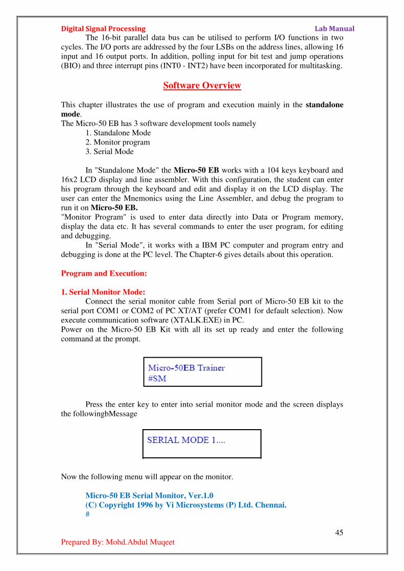
Power on the Micro-50 EB Kit with all its set up ready and enter the following
command at the prompt.
Press the enter key to enter into serial monitor mode and the screen displays
the followingbMessage
Now the following menu will appear on the monitor.
Micro-50 EB Serial Monitor, Ver.1.0
(C) Copyright 1996 by Vi Microsystems (P) Ltd. Chennai. #
Digital Signal Processing Lab Manual
46
Prepared By: Mohd.Abdul Muqeet
Now enter "HE" to view the help menu of the serial monitor.
To assemble the program given in the example enter "AS" at the prompt and press the
Enter Key, the screen displays the following message.
#Micro-50 EB Line Assembler, Version 2.0 Enter Address:
Now enter the program memory starting address "C000H" and press Enter Key. Now
the screen display next consequent message as
C000H
Enter the mnemonics of the program sequentially viewing opcodes of the respective
mnemonics after pressing enter key.
On completion of assembling enter dot (.) and press the enter key to come out to
prompt.
To execute the program use the command "GO C000" and press the Enter
Key, where C000 is program memory starting address.
To abort the execution, press the reset switch once to reset the Micro-50 Kit. Now
enter "SM" in Micro-50 EB trainer to re-enter into serial mode. To verify the
execution, dump the data memory from 8000H to 9000H using "DD" command. This
operation is same as Line assembler in standalone mode.
Note:
1) At any occasion to abort the serial monitor from the execution of the
program press the reset switch of Micro-50 EB kit.
2) To quit of serial monitor mode enter "QU" at the prompt and press enter
key.
Digital Signal Processing Lab Manual
47
Prepared By: Mohd.Abdul Muqeet
Experiment – 7
Aim: To perform 16 bit addition and Integer Multiplication using DSP Trainer Kit
(TMS 320C50PQ57).
Apparatus: PC, DSP Trainer Kit (TMS 320C50PQ57).
Theory: This experiment mainly described about how to construct the TMS320C50
assembly program using line assembler in the Monitor mode for Arithmetic
manipulations and usage of various instruction of TMS320C50 processor. Examples
of Arithmetic manipulations and usage of Instruction of TMS320C50 are given here.
Numerical analysis, floating point computations or other operations may require
arithmetic to be executed with more than 32-bits of precision. Since, the TMS320C50
is 16-bit fixed-point processor; software is required for the extended precision of
arithmetic operations. For proper operation, the overflow mode bit should be reset
(OVM = 0) so that the accumulator result will not be loaded with the saturation value.
Algorithm:
Addition: In this example, two 16-bit numbers will be added as shown below:
X0
+ Y0
-----------------
W0
Where all the numbers X0 & Y0 are 16-bit numbers. TMS320C50 has provision to
add two 16-bit numbers.
First load X0 in higher accumulator using LACC instruction and add Y0 with
accumulator by using ADD instruction.
Integer Multiplication:
The TMS320C50 hardware multiplier normally performs two's complement
16-bit by 16-bit multiplies and produces a 32-bit result in a single processor cycle. To
multiply two operands, one operand must be loaded into the T-register. The second
operand is moved by the multiply instruction to the multiplier, which then produces
the product in the P-register. Before another
multiply can be performed, the content of the P-register should be moved to the
accumulator or should be stored in data memory.
The following program stores the data 37A at data memory 8000 and the data
12E at the data memory address 8001. The instruction LT OP1 (0000h) loads the first
operand from dma 8000 to T register. The instruction MPY OP2 (0001h) multiplies
the content of dma 8001 with the T register. The result is stored in P register. The
instruction PAC transfers the content of P register to accumulator. The SACL and
SACH instructions store the lower and higher order results in dma 8002 and 8003.
Procedure:
1) Open the C50 Debugger software from the desktop.
2) Click the serial port settings and select auto detect.
Serial>Port Settings>AutoDetect
Digital Signal Processing Lab Manual
48
Prepared By: Mohd.Abdul Muqeet
3) It won’t detect at first attempt then reset the kit using reset button and Type SM
using kit’s keyboard and press Enter.
4) Again Select auto detect then it will detect.
5) Select New Project in C50 Debugger Software, give name to project.
6) Create New Assembly File from the File Tab of C50 Debugger.
File>New>Assembly File
7) Type the Program in the above file and save it as filename.asm
*Select filename as Project Name
8) Go to Project Folder and right click on Assembly folder and add the filename.asm
to it.
9) Right Click on the CMD Files folder and add Micro50.cmd to it.
10) Save the Project, Build the Project.
11) Load the Program using Serial Tab.
Load Program>Browse Corresponding ascii file name whose name is same as
name of program.
12) Reset the Kit and Type SM on kit using Kit’s Keyboard.
13) Now access the Program Memory and Data Memory by using Communication
Window.
Select Serial>Communication Window
14) After successfully downloading read the Message.
PI C000-Downloading from Host in Communication Window.
15) Type SD 8000 and press enter then enter the Inputs.
Ex: SD 8000:1234-3333 where 1234 is old data and 3333 is new data.
16) For two values press enter 3 times.
17) Then type dot. to come out.
18) Type GO C000 and press enter. See the message Executing….
19) Reset the Kit and Type SM using the Kits Keyboard.
20) Type SD 8002, press enter and observe the outputs.
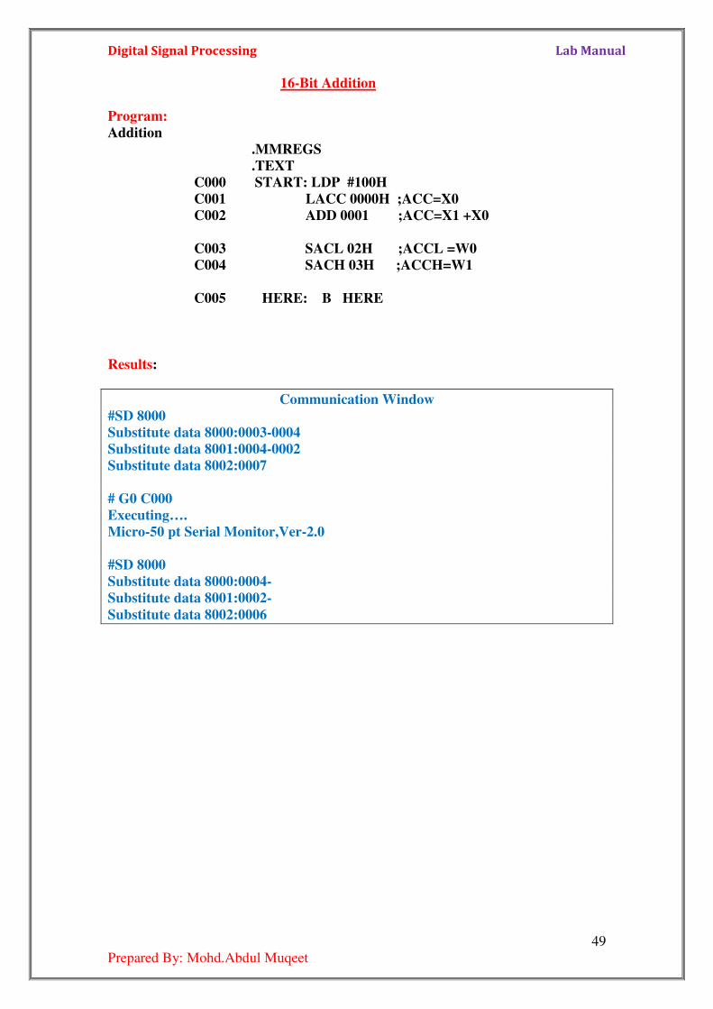
Digital Signal Processing Lab Manual
49
Prepared By: Mohd.Abdul Muqeet
16-Bit Addition
Program:
Addition
.MMREGS
.TEXT
C000 START: LDP #100H
C001 LACC 0000H ;ACC=X0
C002 ADD 0001 ;ACC=X1 +X0
C003 SACL 02H ;ACCL =W0
C004 SACH 03H ;ACCH=W1
C005 HERE: B HERE
Results:
Communication Window
#SD 8000
Substitute data 8000:0003-0004
Substitute data 8001:0004-0002
Substitute data 8002:0007
# G0 C000
Executing….
Micro-50 pt Serial Monitor,Ver-2.0
#SD 8000
Substitute data 8000:0004-
Substitute data 8001:0002-
Substitute data 8002:0006
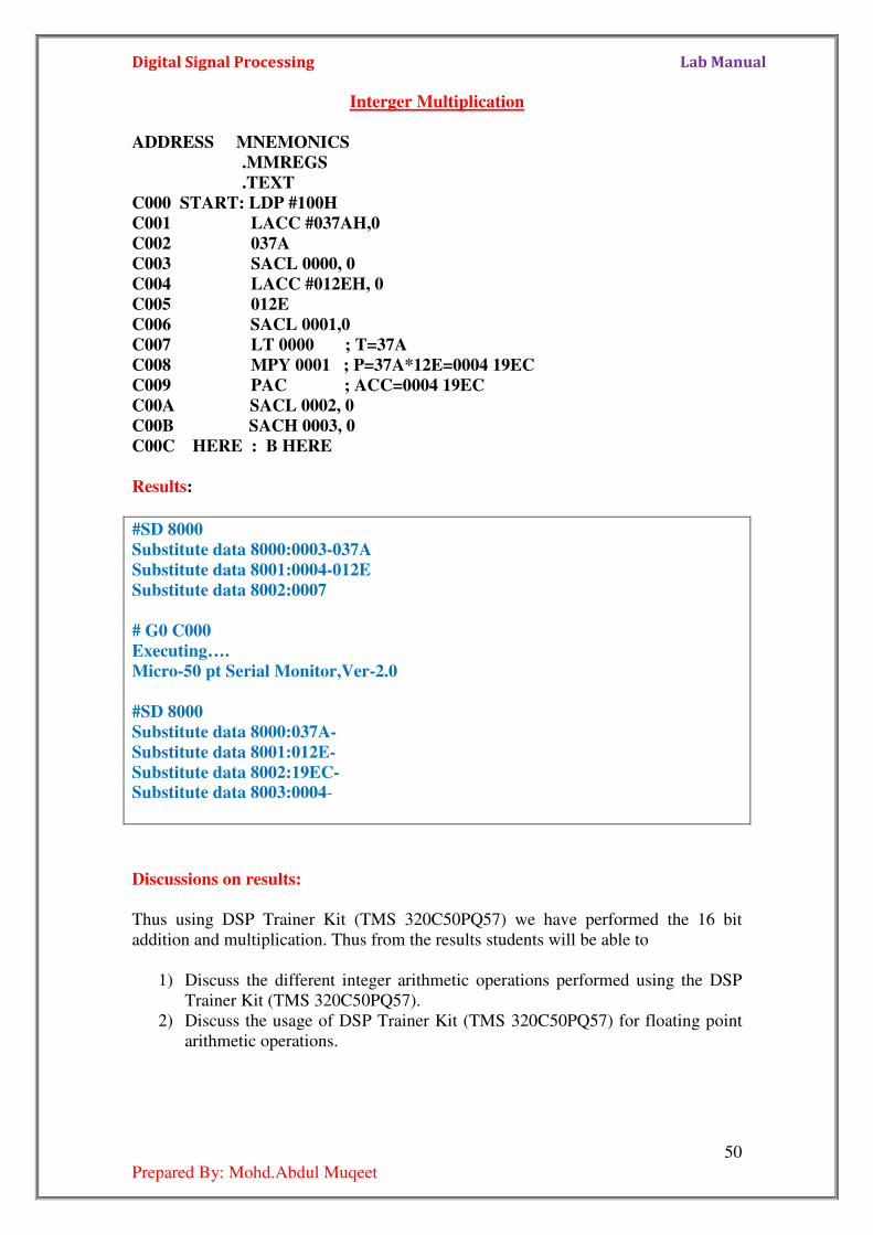
Digital Signal Processing Lab Manual
50
Prepared By: Mohd.Abdul Muqeet
Interger Multiplication
ADDRESS MNEMONICS
.MMREGS
.TEXT
C000 START: LDP #100H
C001 LACC #037AH,0
C002 037A
C003 SACL 0000, 0
C004 LACC #012EH, 0
C005 012E
C006 SACL 0001,0
C007 LT 0000 ; T=37A
C008 MPY 0001 ; P=37A*12E=0004 19EC
C009 PAC ; ACC=0004 19EC
C00A SACL 0002, 0
C00B SACH 0003, 0
C00C HERE : B HERE
Results:
#SD 8000
Substitute data 8000:0003-037A
Substitute data 8001:0004-012E
Substitute data 8002:0007
# G0 C000
Executing….
Micro-50 pt Serial Monitor,Ver-2.0
#SD 8000
Substitute data 8000:037A-
Substitute data 8001:012E-
Substitute data 8002:19EC- Substitute data 8003:0004-
Discussions on results:
Thus using DSP Trainer Kit (TMS 320C50PQ57) we have performed the 16 bit
addition and multiplication. Thus from the results students will be able to
1) Discuss the different integer arithmetic operations performed using the DSP
Trainer Kit (TMS 320C50PQ57).
2) Discuss the usage of DSP Trainer Kit (TMS 320C50PQ57) for floating point
arithmetic operations.

Digital Signal Processing Lab Manual
51
Prepared By: Mohd.Abdul Muqeet
Experiment – 8
Aim: To generate Triangular, and Square Waveforms using DSP Trainer Kit (TMS
320C50PQ57).
Apparatus: PC, DSP Trainer Kit (TMS 320C50PQ57).
Theory: The SPLK instruction allows a full 16-bit pattern to be written into any
memory location. The parallel logic unit (PLU) supports this bit manipulation
independently of the ALU so that the ACC is un affected. In this programme, LDP
instruction is used to load data memory pointer from 8000.
Algorithm:
Triangular Waveform:
1) Load data pointer with the current page number in which we want to store
local variable.
2) Use SPLK to load the value of the temporary register.
3) Under the label CONT1, load the auxiliary register ar2 with the contents of
frequency.
4) Under the label CONT1 initialize count as 04h.
5) Load accumulator register with temporary register value.
6) Add it with value of amplitude.
7) And store back it to temporary register.
8) Check current auxiliary register value for zero, if not equal to zero go back to
label COUNT, otherwise go to next instruction.
9) Again load the auxiliary register ar2 with the contents of frequency.
10) Again out count as 04h.
11) Load accumulator register with temporary register value.
12) Subtract it with value of amplitude.
13) And again store back it to temporary register.
14) Multiply the auxiliary register with the temp register value.
15) Check current auxiliary register value for zero, if not equal to zero go back to
label COUNTX, otherwise go to next instruction.
16) Go back to label COUNT1 to repeat the algorithm continuously.
Square Waveform:
1) Load data pointer with the current page number in which we want to store
local variable.
Digital Signal Processing Lab Manual
52
Prepared By: Mohd.Abdul Muqeet
2) Use SPLK to load the value of the temporary register with value #7FFFH
3) Output the valued through DAC port.
4) Call DELAY label.
5) Use SPLK to load the value of the another temporary register with value
#0FFFH
6) Output the valued through DAC port.
7) Again Call DELAY label.
8) In label DELAY load the Auxiliary Register AR3 with a value FF.
9) Multiply this auxiliary register AR3 value with the same value
10) In label BACK decrement the resultant value of above multiplication by one and
check for not equal to zero. Repeat this procedure till the result goes to zero,
and then return from the loop.
Procedure:
1) Open the C50 Debugger software from the desktop.
2) Click the serial port settings and select auto detect.
Serial>Port Settings>AutoDetect
3) It won’t detect at first attempt then reset the kit using reset button and Type SM
using kit’s keyboard and press Enter.
4) Again Select auto detect then it will detect.
5) Select New Project in C50 Debugger Software, give name to project.
6) Create New Assembly File from the File Tab of C50 Debugger.
File>New>Assembly File
7) Type the Program in the above file and save it as filename.asm
*Select filename as Project Name
8) Go to Project Folder and right click on Assembly folder and add the filename.asm
to it.
9) Right Click on the CMD Files folder and add Micro50.cmd to it.
10) Save the Project, Build the Project.
11) Load the Program using Serial Tab.
Load Program>Browse Corresponding ascii file name whose name is same as
name of program.
12) Reset the Kit and Type SM on kit using Kit’s Keyboard
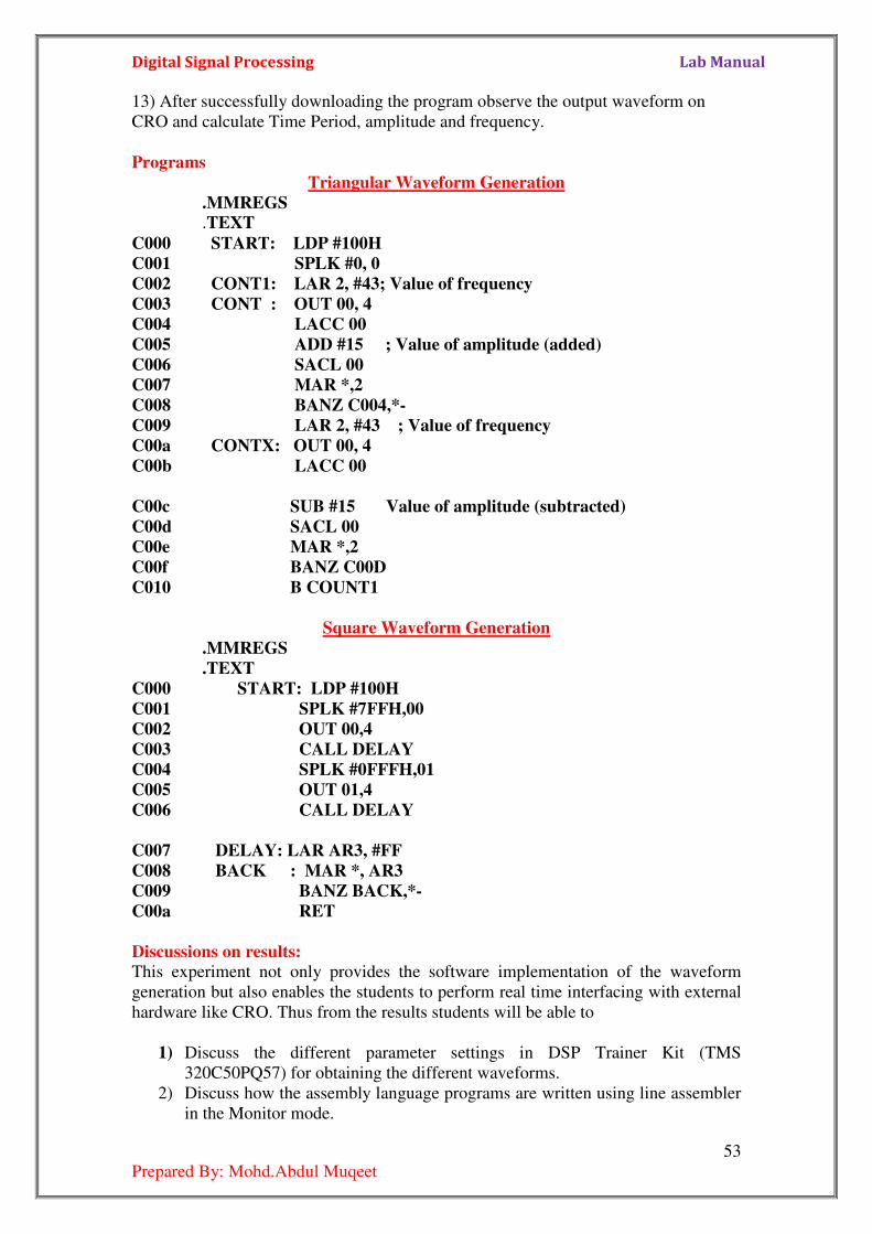
Digital Signal Processing Lab Manual
53
Prepared By: Mohd.Abdul Muqeet
13) After successfully downloading the program observe the output waveform on
CRO and calculate Time Period, amplitude and frequency.
Programs
Triangular Waveform Generation
.MMREGS .TEXT
C000 START: LDP #100H
C001 SPLK #0, 0
C002 CONT1: LAR 2, #43; Value of frequency
C003 CONT : OUT 00, 4
C004 LACC 00
C005 ADD #15 ; Value of amplitude (added)
C006 SACL 00
C007 MAR *,2
C008 BANZ C004,*-
C009 LAR 2, #43 ; Value of frequency
C00a CONTX: OUT 00, 4
C00b LACC 00
C00c SUB #15 Value of amplitude (subtracted)
C00d SACL 00
C00e MAR *,2
C00f BANZ C00D
C010 B COUNT1
Square Waveform Generation
.MMREGS
.TEXT
C000 START: LDP #100H
C001 SPLK #7FFH,00
C002 OUT 00,4
C003 CALL DELAY
C004 SPLK #0FFFH,01
C005 OUT 01,4
C006 CALL DELAY
C007 DELAY: LAR AR3, #FF
C008 BACK : MAR *, AR3
C009 BANZ BACK,*-
C00a RET
Discussions on results: This experiment not only provides the software implementation of the waveform
generation but also enables the students to perform real time interfacing with external
hardware like CRO. Thus from the results students will be able to
1) Discuss the different parameter settings in DSP Trainer Kit (TMS
320C50PQ57) for obtaining the different waveforms.
2) Discuss how the assembly language programs are written using line assembler
in the Monitor mode.
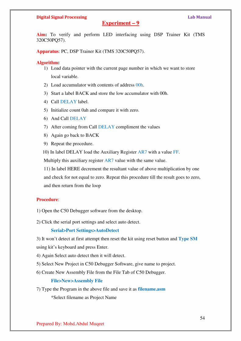
Digital Signal Processing Lab Manual
54
Prepared By: Mohd.Abdul Muqeet
Experiment – 9 Aim: To verify and perform LED interfacing using DSP Trainer Kit (TMS
320C50PQ57).
Apparatus: PC, DSP Trainer Kit (TMS 320C50PQ57).
Algorithm:
1) Load data pointer with the current page number in which we want to store
local variable.
2) Load accumulator with contents of address 00h.
3) Start a label BACK and store the low accumulator with 00h.
4) Call DELAY label.
5) Initialize count 0ah and compare it with zero.
6) And Call DELAY
7) After coming from Call DELAY compliment the values
8) Again go back to BACK
9) Repeat the procedure.
10) In label DELAY load the Auxiliary Register AR7 with a value FF.
Multiply this auxiliary register AR7 value with the same value.
11) In label HERE decrement the resultant value of above multiplication by one
and check for not equal to zero. Repeat this procedure till the result goes to zero,
and then return from the loop
Procedure:
1) Open the C50 Debugger software from the desktop.
2) Click the serial port settings and select auto detect.
Serial>Port Settings>AutoDetect
3) It won’t detect at first attempt then reset the kit using reset button and Type SM
using kit’s keyboard and press Enter.
4) Again Select auto detect then it will detect.
5) Select New Project in C50 Debugger Software, give name to project.
6) Create New Assembly File from the File Tab of C50 Debugger.
File>New>Assembly File
7) Type the Program in the above file and save it as filename.asm
*Select filename as Project Name
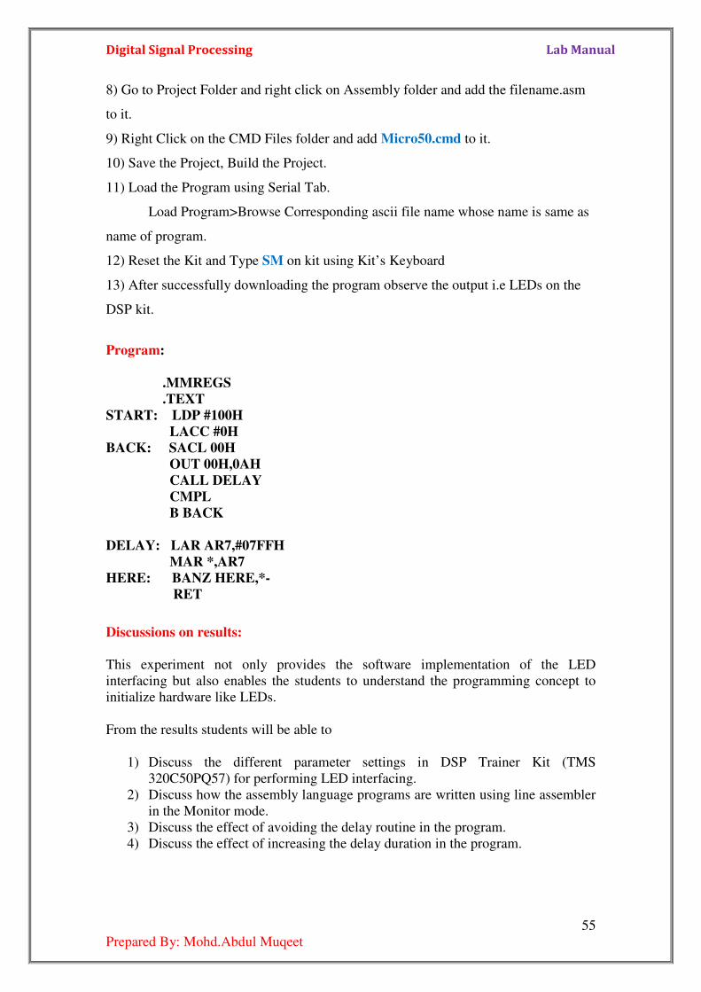
Digital Signal Processing Lab Manual
55
Prepared By: Mohd.Abdul Muqeet
8) Go to Project Folder and right click on Assembly folder and add the filename.asm
to it.
9) Right Click on the CMD Files folder and add Micro50.cmd to it.
10) Save the Project, Build the Project.
11) Load the Program using Serial Tab.
Load Program>Browse Corresponding ascii file name whose name is same as
name of program.
12) Reset the Kit and Type SM on kit using Kit’s Keyboard
13) After successfully downloading the program observe the output i.e LEDs on the
DSP kit.
Program:
.MMREGS
.TEXT
START: LDP #100H
LACC #0H
BACK: SACL 00H
OUT 00H,0AH
CALL DELAY
CMPL
B BACK
DELAY: LAR AR7,#07FFH
MAR *,AR7
HERE: BANZ HERE,*-
RET
Discussions on results:
This experiment not only provides the software implementation of the LED
interfacing but also enables the students to understand the programming concept to
initialize hardware like LEDs.
From the results students will be able to
1) Discuss the different parameter settings in DSP Trainer Kit (TMS
320C50PQ57) for performing LED interfacing.
2) Discuss how the assembly language programs are written using line assembler
in the Monitor mode.
3) Discuss the effect of avoiding the delay routine in the program.
4) Discuss the effect of increasing the delay duration in the program.
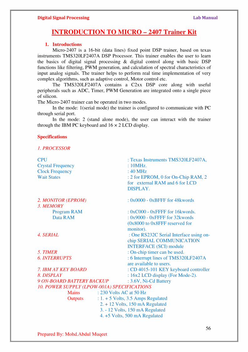
Digital Signal Processing Lab Manual
56
Prepared By: Mohd.Abdul Muqeet
INTRODUCTION TO MICRO – 2407 Trainer Kit
1. Introductions Micro-2407 is a 16-bit (data lines) fixed point DSP trainer, based on texas
instruments TMS320LF2407A DSP Processor. This trainer enables the user to learn
the basics of digital signal processing & digital control along with basic DSP
functions like filtering, PWM generation, and calculation of spectral characteristics of
input analog signals. The trainer helps to perform real time implementation of very
complex algorithms, such as adaptive control, Motor control etc.
The TMS320LF2407A contains a C2xx DSP core along with useful
peripherals such as ADC, Timer, PWM Generation are integrated onto a single piece
of silicon.
The Micro-2407 trainer can be operated in two modes.
In the mode: 1(serial mode) the trainer is configured to communicate with PC
through serial port.
In the mode: 2 (stand alone mode), the user can interact with the trainer
through the IBM PC keyboard and 16 × 2 LCD display.
Specifications
1. PROCESSOR
CPU : Texas Instruments TMS320LF2407A,
Crystal Frequency : 10MHz.
Clock Frequency : 40 MHz
Wait States : 2 for EPROM, 0 for On-Chip RAM, 2
for external RAM and 6 for LCD
DISPLAY.
2. MONITOR (EPROM) : 0x0000 - 0xBFFF for 48kwords
3. MEMORY
Program RAM : 0xC000 - 0xFFFF for 16kwords.
Data RAM : 0x9000 - 0xFFFF for 32kwords
(0x8000 to 0x8FFF reserved for
monitor).
4. SERIAL : One RS232C Serial Interface using on-
chip SERIAL COMMUNICATION
INTERFACE (SCI) module
5. TIMER : On-chip timer can be used.
6. INTERRUPTS : 6 Interrupt lines of TMS320LF2407A
are available to users.
7. IBM AT KEY BOARD : CD 4015-101 KEY keyboard controller
8. DISPLAY : 16x2 LCD display (For Mode-2).
9 ON-BOARD BATTERY BACKUP : 3.6V, Ni-Cd Battery
10. POWER SUPPLY (LPOW-001A) SPECIFICATIONS
Mains : 230 Volts AC at 50 Hz
Outputs : 1. + 5 Volts, 3.5 Amps Regulated
2. + 12 Volts, 150 mA Regulated
3. - 12 Volts, 150 mA Regulated
4. +5 Volts, 500 mA Regulated
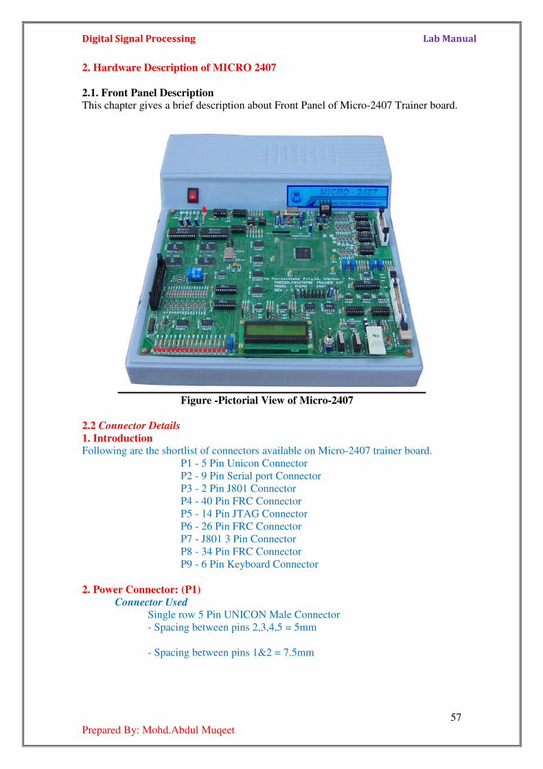
Digital Signal Processing Lab Manual
57
Prepared By: Mohd.Abdul Muqeet
2. Hardware Description of MICRO 2407
2.1. Front Panel Description This chapter gives a brief description about Front Panel of Micro-2407 Trainer board.
Figure -Pictorial View of Micro-2407
2.2 Connector Details
1. Introduction Following are the shortlist of connectors available on Micro-2407 trainer board.
P1 - 5 Pin Unicon Connector
P2 - 9 Pin Serial port Connector
P3 - 2 Pin J801 Connector
P4 - 40 Pin FRC Connector
P5 - 14 Pin JTAG Connector
P6 - 26 Pin FRC Connector
P7 - J801 3 Pin Connector
P8 - 34 Pin FRC Connector
P9 - 6 Pin Keyboard Connector
2. Power Connector: (P1)
Connector Used Single row 5 Pin UNICON Male Connector
- Spacing between pins 2,3,4,5 = 5mm
- Spacing between pins 1&2 = 7.5mm
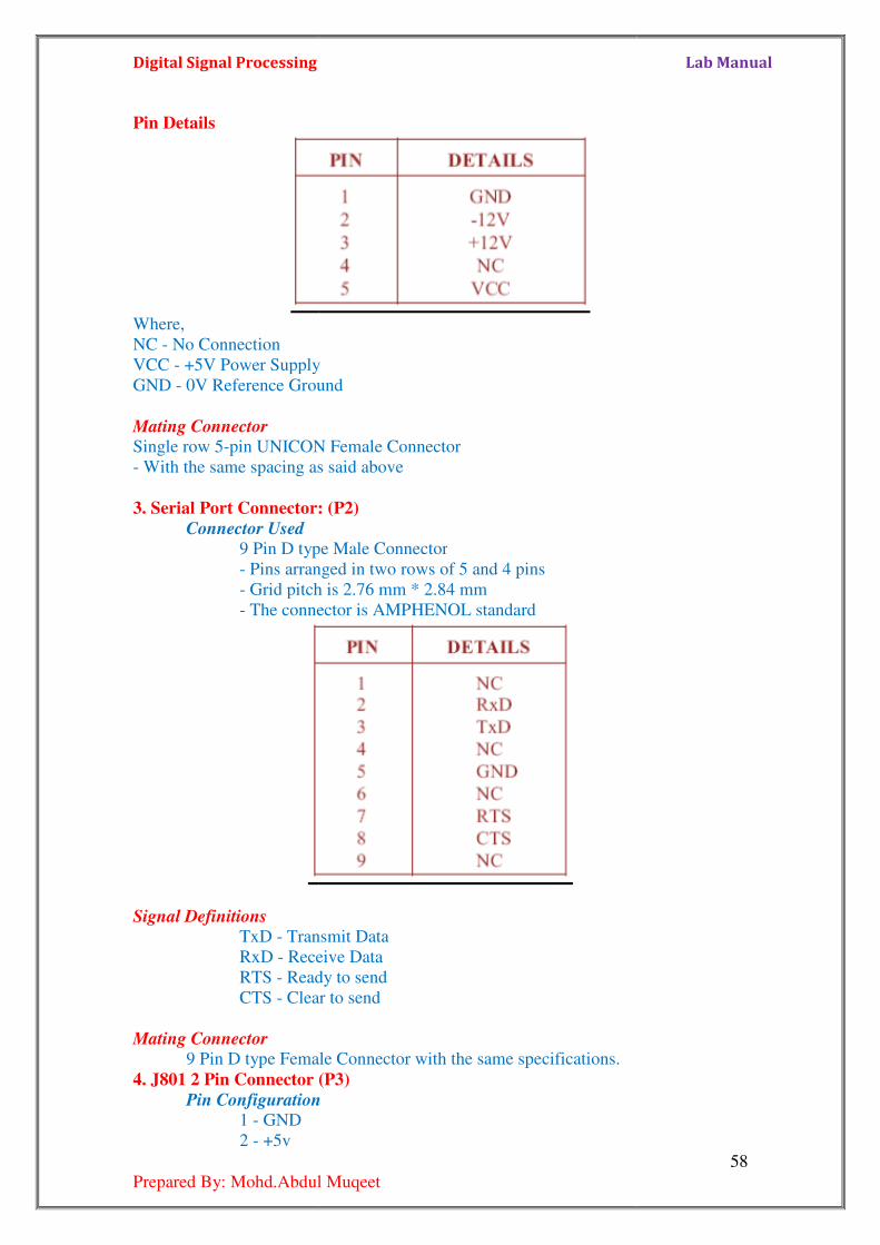
Digital Signal Processing
Prepared By: Mohd.Abdul Muqeet
Pin Details
Where,
NC - No Connection
VCC - +5V Power Supply
GND - 0V Reference Ground
Mating Connector Single row 5-pin UNICON Female Connector
- With the same spacing as said above
3. Serial Port Connector: (P2)
Connector Used 9 Pin D type Male Connector
- Pins arranged in two rows of 5 and 4 pins
- Grid pitch is 2.76 mm * 2.84 mm
- The connector is AMPHENOL standard
Signal Definitions TxD - Transmit Data
RxD - Receive Data
RTS - Ready to send
CTS - Clear to send
Mating Connector 9 Pin D type Female Connector
4. J801 2 Pin Connector
Pin Configuration1 - GND
2 - +5v
Prepared By: Mohd.Abdul Muqeet
+5V Power Supply
0V Reference Ground
pin UNICON Female Connector
With the same spacing as said above
: (P2)
9 Pin D type Male Connector
arranged in two rows of 5 and 4 pins
Grid pitch is 2.76 mm * 2.84 mm
The connector is AMPHENOL standard
Transmit Data
Receive Data
Ready to send
Clear to send
9 Pin D type Female Connector with the same specifications.
(P3)
Pin Configuration
Lab Manual
58
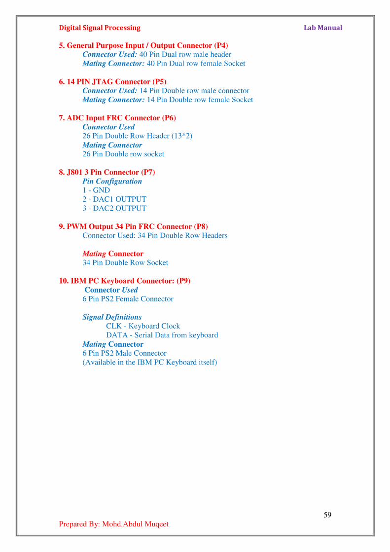
Digital Signal Processing Lab Manual
59
Prepared By: Mohd.Abdul Muqeet
5. General Purpose Input / Output Connector (P4) Connector Used: 40 Pin Dual row male header
Mating Connector: 40 Pin Dual row female Socket
6. 14 PIN JTAG Connector (P5) Connector Used: 14 Pin Double row male connector
Mating Connector: 14 Pin Double row female Socket
7. ADC Input FRC Connector (P6)
Connector Used 26 Pin Double Row Header (13*2)
Mating Connector 26 Pin Double row socket
8. J801 3 Pin Connector (P7)
Pin Configuration 1 - GND
2 - DAC1 OUTPUT
3 - DAC2 OUTPUT
9. PWM Output 34 Pin FRC Connector (P8) Connector Used: 34 Pin Double Row Headers
Mating Connector 34 Pin Double Row Socket
10. IBM PC Keyboard Connector: (P9)
Connector Used 6 Pin PS2 Female Connector
Signal Definitions
CLK - Keyboard Clock
DATA - Serial Data from keyboard
Mating Connector
6 Pin PS2 Male Connector
(Available in the IBM PC Keyboard itself)
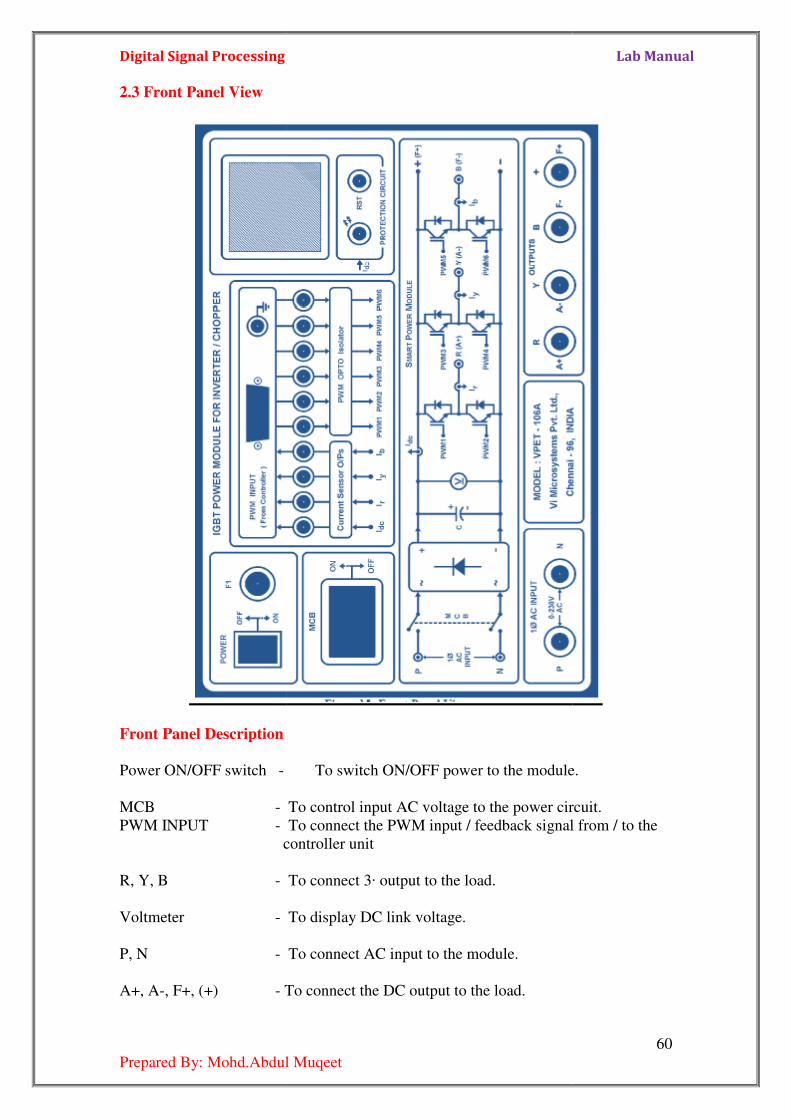
Digital Signal Processing
Prepared By: Mohd.Abdul Muqeet
2.3 Front Panel View
Front Panel Description
Power ON/OFF switch -
MCB -
PWM INPUT -
controller unit
R, Y, B -
Voltmeter -
P, N -
A+, A-, F+, (+) - To connect the DC output to the load.
Prepared By: Mohd.Abdul Muqeet
To switch ON/OFF power to the module.
To control input AC voltage to the power circuit.
To connect the PWM input / feedback signal from / to the
controller unit
To connect 3· output to the load.
To display DC link voltage.
To connect AC input to the module.
To connect the DC output to the load.
Lab Manual
60
To switch ON/OFF power to the module.
To control input AC voltage to the power circuit.
To connect the PWM input / feedback signal from / to the
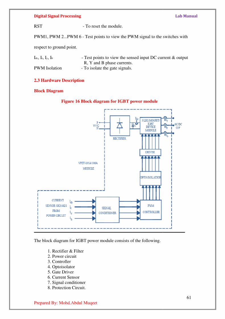
Digital Signal Processing
Prepared By: Mohd.Abdul Muqeet
RST
PWM1, PWM 2...PWM 6
respect to ground point.
Idc, Ir, Iy, Ib
PWM Isolation -
2.3 Hardware Description
Block Diagram
Figure 16 Block diagram for IGBT power module
The block diagram for IGBT power module consists of the following.
1. Rectifier & Filter
2. Power circuit
3. Controller
4. Optoisolator
5. Gate Driver
6. Current Sensor
7. Signal conditioner
8. Protection Circuit.
Prepared By: Mohd.Abdul Muqeet
- To reset the module.
- Test points to view the PWM signal to the switches with
- Test points to view the sensed input DC current & output
R, Y and B phase currents.
- To isolate the gate signals.
2.3 Hardware Description
Figure 16 Block diagram for IGBT power module
The block diagram for IGBT power module consists of the following.
1. Rectifier & Filter
7. Signal conditioner
8. Protection Circuit.
Lab Manual
61
Test points to view the PWM signal to the switches with
Test points to view the sensed input DC current & output
Digital Signal Processing Lab Manual
62
Prepared By: Mohd.Abdul Muqeet
Block Diagram Description
1. Rectifier & Filter The input AC voltage is rectified by the Diode Bridge Rectifier circuit. The
rectified DC voltage is fed to the power circuit through a filter capacitor. The filter
capacitor eliminates the unwanted ripple in the Dc input.
2. Power Circuit The Power circuit consists of three leg IGBT circuit. IGBT switch is used as a
switching device in the power circuit. The PWM signal from the driver IC is fed to the
gate of the switch. The output from the power circuit is given to the load. The output
may be either AC/DC depending on the inverter/chopper mode of operation.
3. Controller The PWM signal to the IGBT switches is generated by the controller unit. The
controller may be any processor. The PWM signal from the controller is fed to the
module through the connector provided on the front panel. In this implementation,
controller is used PWM generation.
4. Optoisolator (6N137)
The function of Optoisolator is to isolate the control circuit from power circuit.PWM signal from the controller is not directly fed to the power circuit in order
to protect the PWM signal it is essential to provide isolation circuit between power
circuit and control circuit or else the high power components may damage the low
power PWM circuit components.
5. Gate Driver (IR2110) An IGBT drive circuit is designed to connect the gate directly to a voltage
bus with no intervening resistance other than the impedance of the drive circuit
switch. Gate driver acts as a high-power buffer stage between the PWM output of
the control device and gates of the primary power switching IGBT.
6. Current Sensor IGBT power module output current is not directly fed to control (Protection)
circuits. The sensor used for sensing current works on the principle of Hall Effect.
Hence these sensors are called Hall Effect transducer. Hall Effect transducer output
current depends upon transducer primary and secondary winding ratio. The turn’s
ratio represents the ratio of the number of primary turns to the number of secondary
turns. A Hall effect current transducer senses the current IDC, Ir(R), Iy(Y) Ib(B).
7. Signal Conditioner The signal from the current sensor is fed back to the controller unit. The gain
of the current signals has to be improved to achieve controller requirements. So the
signal needs to be conditioned in the signal conditioner circuits.
8. Protection Circuit In the protection circuit the DC current Idc is sensed. If the I dc value increases
than the limit, the protection circuit activates and cuts the PWM to the switches in the
module. The LED glows to indicate the system shut down condition. The system can
be reset by the RST press button provided on the front panel. Now the LED switches
OFF. Again the PWM signal should be applied to the system.
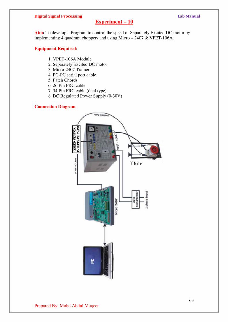
Digital Signal Processing Lab Manual
63
Prepared By: Mohd.Abdul Muqeet
Experiment – 10 Aim: To develop a Program to control the speed of Separately Excited DC motor by
implementing 4 quadrant choppers and using Micro – 2407 & VPET-106A.
Equipment Required:
1. VPET-106A Module
2. Separately Excited DC motor
3. Micro-2407 Trainer
4. PC-PC serial port cable.
5. Patch Chords
6. 26 Pin FRC cable
7. 34 Pin FRC cable (dual type)
8. DC Regulated Power Supply (0-30V)
Connection Diagram
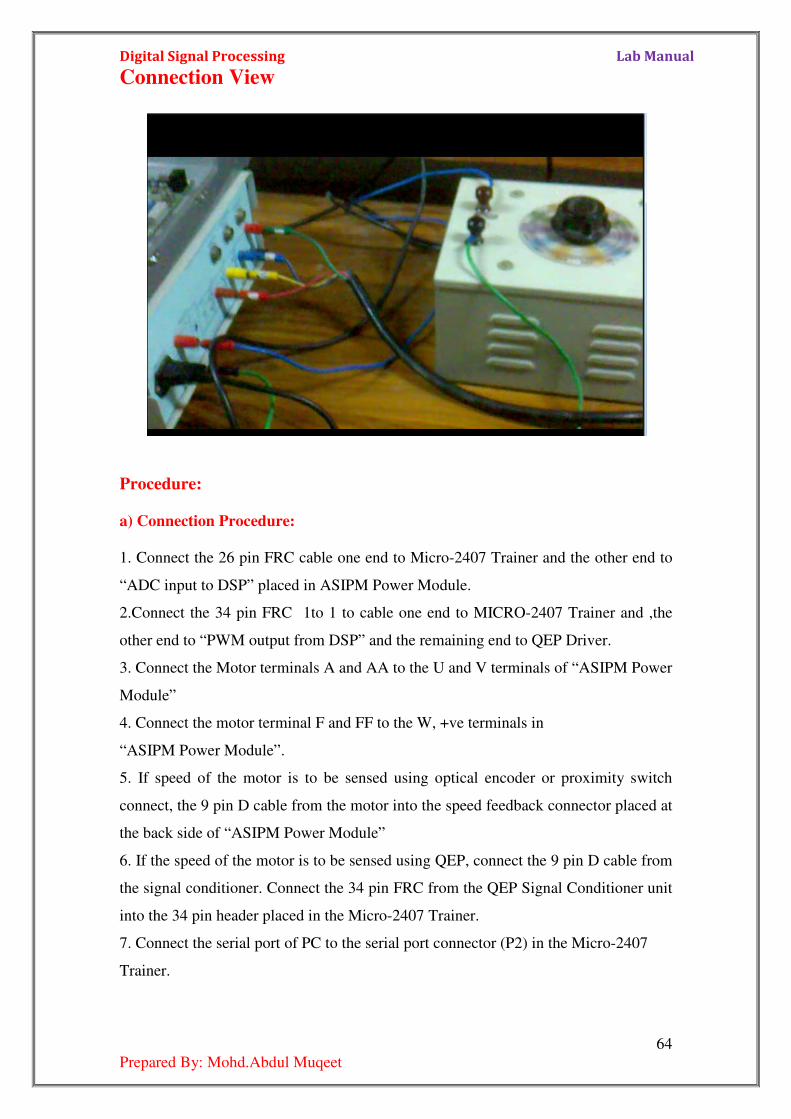
Digital Signal Processing Lab Manual
64
Prepared By: Mohd.Abdul Muqeet
Connection View
Procedure:
a) Connection Procedure:
1. Connect the 26 pin FRC cable one end to Micro-2407 Trainer and the other end to
“ADC input to DSP” placed in ASIPM Power Module.
2.Connect the 34 pin FRC 1to 1 to cable one end to MICRO-2407 Trainer and ,the
other end to “PWM output from DSP” and the remaining end to QEP Driver.
3. Connect the Motor terminals A and AA to the U and V terminals of “ASIPM Power
Module”
4. Connect the motor terminal F and FF to the W, +ve terminals in
“ASIPM Power Module”.
5. If speed of the motor is to be sensed using optical encoder or proximity switch
connect, the 9 pin D cable from the motor into the speed feedback connector placed at
the back side of “ASIPM Power Module”
6. If the speed of the motor is to be sensed using QEP, connect the 9 pin D cable from
the signal conditioner. Connect the 34 pin FRC from the QEP Signal Conditioner unit
into the 34 pin header placed in the Micro-2407 Trainer.
7. Connect the serial port of PC to the serial port connector (P2) in the Micro-2407
Trainer.
Digital Signal Processing Lab Manual
65
Prepared By: Mohd.Abdul Muqeet
8. Set the SW1 Switch in the Micro-2407 Trainer downward direction, it works in
serial monitor mode.
b) Experiment Procedure
1. Verify the connection as per the connection procedure and wiring diagram.
2. Switch ON the Micro-2407 Trainer.
3. Power ON the “ASIPM Power Module” power ON power switch.
4. Check whether shut down LED “SD” LED glows, press the Reset switch, the LED
gets OFF.
Open Loop Control of Dc Motor
1. Select C2407 from your target directory or from your desktop in PC.
2. Now the ‘configure the port open, select the port to which Micro-2407 trainer and
press enter key.
3. Select the open loop Menu in that select DC motor followed by Chop\v/up.
4. The plot of ‘speed and current’ in now available in PC.
5. Select the send, now transmission completed message appears given ok.
6. Select the Execute, now “Kp and Ki parameter settings window appears. Enter the
Kp and Ki values and given OK.
7. Now the current value of speed and current is displayed.
8. Vary the speed of motor by pressing SW2 and SW3 key placed in the Micro-2407
trainer and note down the corresponding output voltage.
Closed Loop Control of DC Motor.
1. Select the “C2407” from the desktop in PC.
2. Now the “Configure port open “open, select the port to which Micro-2407 Trainer
and press “Enter Key”.
3. Select the Closed Loop Menu in that select DC Motor followed by Chop\v/up.
4. The plot of “Speed and current” is now available in PC.
5. Select the SEND, now transmission completed message appears given ok.
6. Select the EXECUTE; now the “Kp and Ki Parameter Settings” windows appears.
Enter the Kp and Ki values and given OK.
7. Now the current value of speed and current is displayed in PC.
8. Vary the speed of motor by pressing SW2 or SW3 key placed in the Micro-2407
Trainer and note down the corresponding voltage.
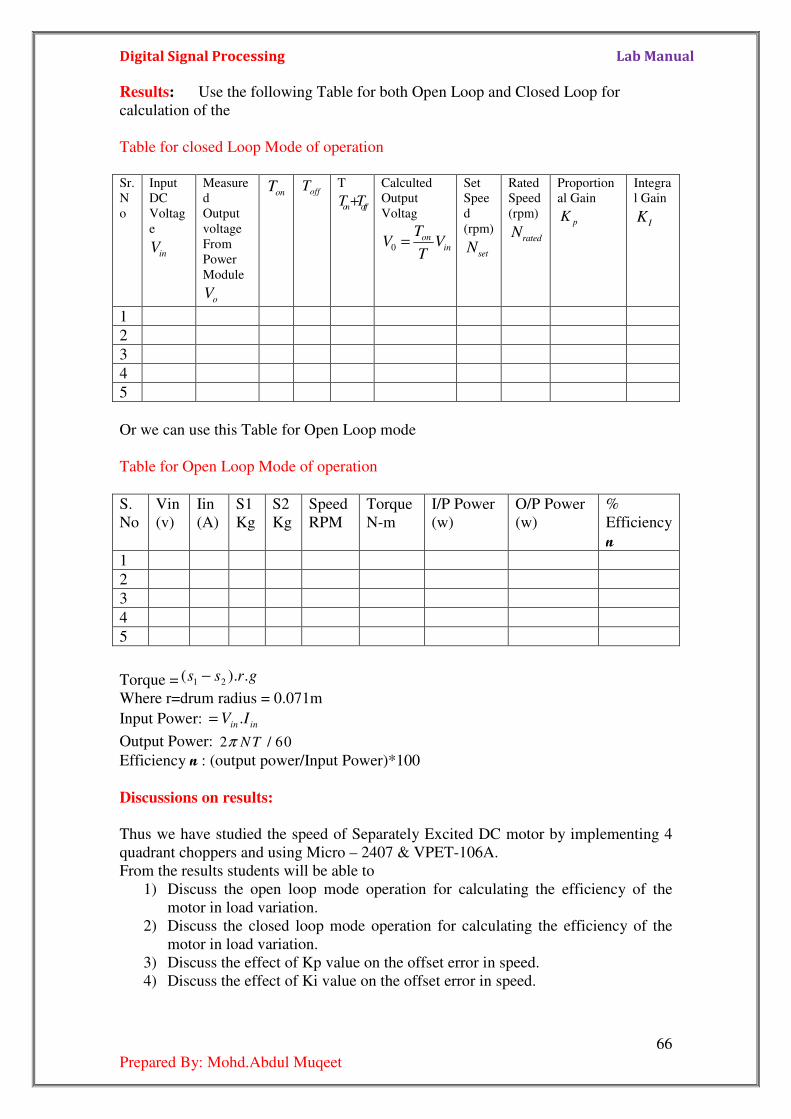
Digital Signal Processing Lab Manual
66
Prepared By: Mohd.Abdul Muqeet
Results: Use the following Table for both Open Loop and Closed Loop for
calculation of the
Table for closed Loop Mode of operation
Sr.
N
o
Input
DC
Voltag
e
inV
Measure
d
Output
voltage
From
Power
Module
oV
onT
offT
T
on offT T+
Calculted
Output
Voltag
0on
in
TV V
T=
Set
Spee
d
(rpm)
setN
Rated
Speed
(rpm)
ratedN
Proportion
al Gain
pK
Integra
l Gain
IK
1
2
3
4
5
Or we can use this Table for Open Loop mode
Table for Open Loop Mode of operation
S.
No
Vin
(v)
Iin
(A)
S1
Kg
S2
Kg
Speed
RPM
Torque
N-m
I/P Power
(w)
O/P Power
(w)
%
Efficiency
n
1
2
3
4
5
Torque = 1 2( ). .s s r g−
Where r=drum radius = 0.071m
Input Power: .in inV I=
Output Power: 2 / 60N Tπ
Efficiency n : (output power/Input Power)*100
Discussions on results:
Thus we have studied the speed of Separately Excited DC motor by implementing 4
quadrant choppers and using Micro – 2407 & VPET-106A.
From the results students will be able to
1) Discuss the open loop mode operation for calculating the efficiency of the
motor in load variation.
2) Discuss the closed loop mode operation for calculating the efficiency of the
motor in load variation.
3) Discuss the effect of Kp value on the offset error in speed.
4) Discuss the effect of Ki value on the offset error in speed.
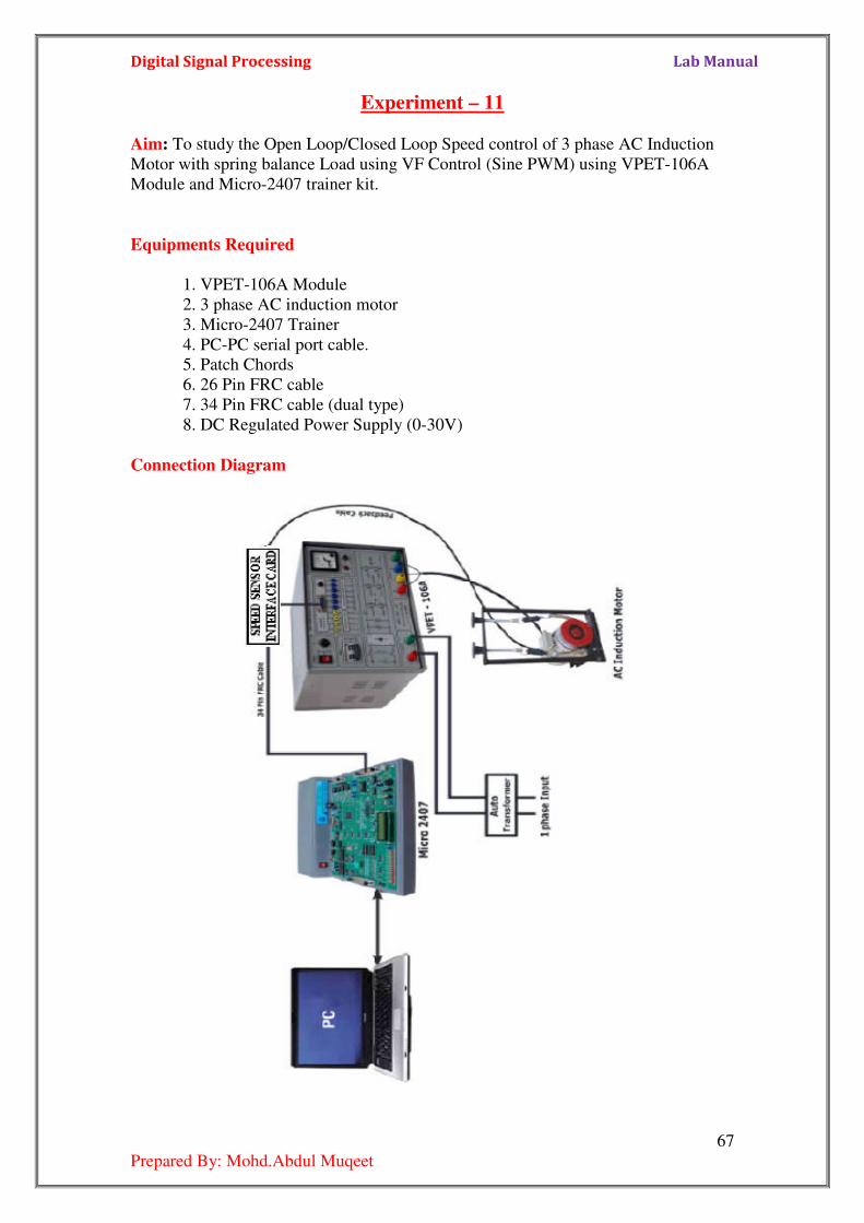
Digital Signal Processing Lab Manual
67
Prepared By: Mohd.Abdul Muqeet
Experiment – 11 Aim: To study the Open Loop/Closed Loop Speed control of 3 phase AC Induction
Motor with spring balance Load using VF Control (Sine PWM) using VPET-106A
Module and Micro-2407 trainer kit.
Equipments Required
1. VPET-106A Module
2. 3 phase AC induction motor
3. Micro-2407 Trainer
4. PC-PC serial port cable.
5. Patch Chords
6. 26 Pin FRC cable
7. 34 Pin FRC cable (dual type)
8. DC Regulated Power Supply (0-30V)
Connection Diagram
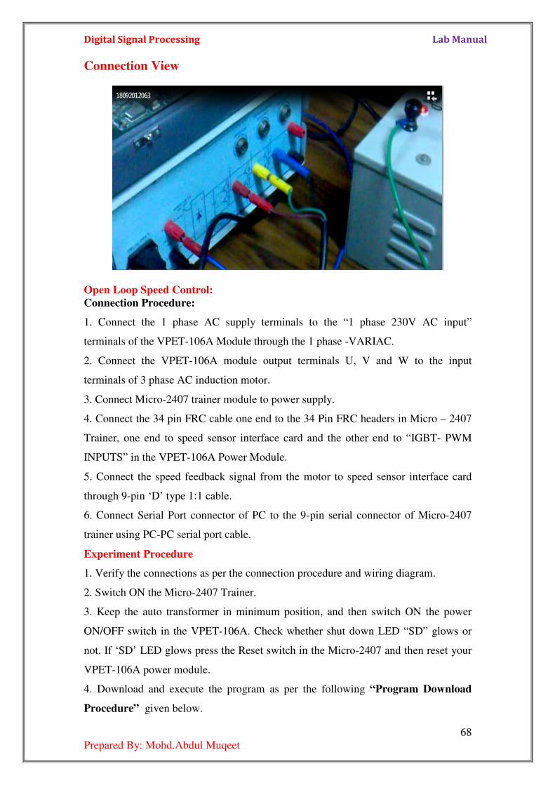
Digital Signal Processing Lab Manual
68
Prepared By: Mohd.Abdul Muqeet
Connection View
Open Loop Speed Control:
Connection Procedure:
1. Connect the 1 phase AC supply terminals to the “1 phase 230V AC input”
terminals of the VPET-106A Module through the 1 phase -VARIAC.
2. Connect the VPET-106A module output terminals U, V and W to the input
terminals of 3 phase AC induction motor.
3. Connect Micro-2407 trainer module to power supply.
4. Connect the 34 pin FRC cable one end to the 34 Pin FRC headers in Micro – 2407
Trainer, one end to speed sensor interface card and the other end to “IGBT- PWM
INPUTS” in the VPET-106A Power Module.
5. Connect the speed feedback signal from the motor to speed sensor interface card
through 9-pin ‘D’ type 1:1 cable.
6. Connect Serial Port connector of PC to the 9-pin serial connector of Micro-2407
trainer using PC-PC serial port cable.
Experiment Procedure
1. Verify the connections as per the connection procedure and wiring diagram.
2. Switch ON the Micro-2407 Trainer.
3. Keep the auto transformer in minimum position, and then switch ON the power
ON/OFF switch in the VPET-106A. Check whether shut down LED “SD” glows or
not. If ‘SD’ LED glows press the Reset switch in the Micro-2407 and then reset your
VPET-106A power module.
4. Download and execute the program as per the following “Program Download
Procedure” given below.
Digital Signal Processing Lab Manual
69
Prepared By: Mohd.Abdul Muqeet
5. Switch ON the MCB, then slowly increases the 3 phase AC input to the module
through the auto transformer and set the DC link voltage at 350V.
6. Switch ON the PC and then press Reset Switch of the Micro-2407 Trainer.
Program Download Procedure
1. Double Click C2407 debugger icon from the target directory or from the desktop.
Now the window shows
2. Now configure the serial port settings and press ‘OK’ button. Now the window
shows.
3. Select the required program to be downloaded. For open loop AC motor with
Sine/Tri or space vector Modulation select Open Loop —> AC Motor —> Sine/Tri
or Space vector.
4. Ensure whether the motor is connected or not. Then click ‘OK’.
6. Click ‘Send’.
7. Click ‘OK’ (the particular file will be download to controller).
8. Now the transmission completed message appears, click ‘OK’ and then click
‘EXECUTE’.
9. Check the all PWMs by connecting CRO. Now apply AC voltage though single
phase variac upto 300VDC.
10. Now, the speed value is plotted then speed and frequency numerical values are
displayed.
11. To change the speed of the motor, use the increment/decrement switch in the 2407
kit.
12. To measure i/p voltage of the motor, connect Ac voltmeter (0- 450 V) across U
and V terminals of the VPET-106A and frequency is obtained from the front end
software.
Now check the V/F ratio of the motor.
13. By applying load to the motor, motor speed is not remains constant and it is not
equal to the set speed.
14. To measure the load current of the motor, externally connect one AC ammeter in
series with any one phase.
Closed Loop Speed Control:
Connection Procedure
1. Connect the 1 phase AC supply terminals to the “1 phase 230V AC input”
terminals of the VPET-106A Module through the 1 phase -VARIAC.
Digital Signal Processing Lab Manual
70
Prepared By: Mohd.Abdul Muqeet
2. Connect the VPET-106A module output terminals U, V and W to the input
terminals of 3 phase AC induction motor.
3. Connect Micro-2407 trainer module to power supply.
4. Connect the 34 pin FRC cable one end to the 34 Pin FRC header in Micro – 2407
Trainer, one end to speed sensor interface card and the other end to “IGBT- PWM
INPUTS” in the VPET-106A Power Module.
5. Connect the speed feedback signal from the motor to speed sensor interface card
through 9-pin ‘D’ type 1:1 cable.
6. Connect Serial Port connector of PC to the 9-pin serial connector of Micro-2407
trainer using PC-PC serial port cable.
Experiment Procedure
1. Verify the connections as per the connection procedure and wiring diagram.
2. Switch ON the Micro-2407 Trainer.
3. Keep the auto transformer in minimum position, and then switch ON the power
ON/OFF switch in the VPET-106A. Check whether shut down LED “SD” glows or
not. If ‘SD’ LED glows press the Reset switch in the Micro-2407 and then reset your
VPET-106A power module.
4. Download and execute the program as per the following “Program Download
Procedure” given below
5. Switch ON the MCB, then slowly increases the 3 phase AC input to the module
through the auto transformer and set the DC link voltage at 350V.
6. Switch ON the PC and then press Reset Switch of the Micro-2407 Trainer.
Program Downloading Procedure:
1. Double Click C2407 icon from the target directory or from the desktop. 2. Now
configure the serial port settings and press ‘OK’ button. Now the window shows.
2. Select the required program to be downloaded. For close loop AC motor with
Sine/Tri or space vector Modulation select Close Loop —> AC Motor —> Sine/Tri
or Space vector.
3. Ensure whether the motor is connected or not. Then click ‘OK’.
4. Click ‘Send’ then the window shows below.
5. Click ‘OK’ (the particular file will be download to controller)
6. Now the transmission completed message appears, click ‘OK’ and then click
‘EXECUTE’.
Digital Signal Processing Lab Manual
71
Prepared By: Mohd.Abdul Muqeet
7. Check the all PWMs by connecting CRO. Now apply AC voltage though single
phase variac upto 300VDC.
8. Now, the speed value is plotted then speed and frequency numerical values are
displayed.
9. To change the speed of the motor, use the increment/decrement switch in the 2407
kit.
10. To measure i/p voltage of the motor, connect Ac voltmeter (0- 450 V) across U
and V terminals of the VPET-106A and frequency is obtained from the front end
software. Now check the V/F ratio of the motor.
11. By applying load to the motor, motor speed is remains constant and it is equal to
the set speed.
12. To measure the load current of the motor, externally connect one AC ammeter in
series with any one phase. (Ref: connection diagram).
Results: Use the following Table for Closed Loop mode for operation
Sr.
No
Input
Voltage
inV
Measur
ed
Output
voltage
From
Power
Module
oV
onT offT T
on offT T
Calculted
Output
Voltag
Set
Speed
(rpm)
setN
Rated
Speed
(rpm)
ratedN
pK
IK
1
2
3
4
5
Discussions on results:
Thus the real time interfacing of the Induction motor with Micro-2407 trainer kit is
experimented and speed control of 3 –ph Induction Motor with spring balance Load
using the VPET-106A Module and Micro-2407 trainer kit is performed.
From the results students will be able to
1) Discuss the open loop mode operation for calculating the efficiency of the
motor in load variation.
2) Discuss the closed loop mode operation for calculating the efficiency of the
motor in load variation.
3) Discuss the effect of Kp value on the offset error in speed.
4) Discuss the effect of Ki value on the offset error in speed.
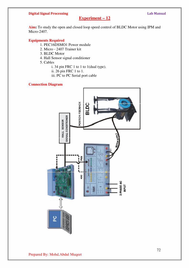
Digital Signal Processing Lab Manual
72
Prepared By: Mohd.Abdul Muqeet
Experiment – 12
Aim: To study the open and closed loop speed control of BLDC Motor using IPM and
Micro-2407.
Equipments Required 1. PEC16DSMO1 Power module
2. Micro - 2407 Trainer kit
3. BLDC Motor
4. Hall Sensor signal conditioner
5. Cables
i. 34 pin FRC 1 to 1 to 1(dual type).
ii. 26 pin FRC 1 to 1.
iii. PC to PC Serial port cable
Connection Diagram

Digital Signal Processing Lab Manual
73
Prepared By: Mohd.Abdul Muqeet
Connection Procedure
1. Connect the three-phase AC supply (MAINS) to i/p of 3NVARIAC.Then 3-phase
VARIAC o/p connect to R, Y and B (3N INPUTS) terminals of PEC16DSMO1
Power Module.
2. Connect the U, V, W terminals (through switching output connector) in the
PEC16DSMO1 Power Module to the 7 - pin supply connector of the Motor (refer
connection diagram)
3. Connect the 17 pin Feedback connector from the Motor into Hall sensor signal
conditioner (Through 9 Pin “D Connector”).
4. Connect the 34 pin FRC cable one end to the 34 Pin FRC header in Micro - 2407
Trainer, one end to Hall Sensor signal conditioner and the other end to “IGBT-PWM
INPUTS” in the PEC16DSMO1 Power Module.
5. Connect the serial port PC-PC cable between PC and Micro - 2407 Trainer.
6. Connect one end of 26 Pin FRC cable to 26 pin connector placed in Micro - 2407
Trainer and the other end to “FEEDBACK INPUTS” in PEC16DSMO1 Power
Module.
Experiment Procedure
1. Verify the connections as per the connection procedure and Wiring Diagram.
2. Switch ON the Micro-2407 DSP Trainer.
3. Power ON the Intelligent Power Module (PEC16DSMO1) and MCB.
4. Check whether shut down LED “SD” glows in the power module or not. If ‘SD’
LED glows press the Reset switch in the front panel, the LED gets OFF.
5. After ensuring all the connections, using VARIAC apply the input voltage slowly
450V DC (DC rail Voltage) which is shown in the power module’s voltmeter.
6. Switch ON the PC and set the switch SW1 in down position (Serial Mode) of
Micro- 2407 DSP Trainer, then press Reset switch.
7. Select the “BLDC Motor Controller” icon in the Desktop.
8. To open port, Select “File” and click “OPEN PORT” as shown below.
9. On Port open the window asks for Port No, Baud Rate, etc., as shown below.
10. In the displayed window, select the connected port (COM 1, 2, 3, or 4) and other
settings are default, port is open for communication
11. Now select the “Motor Controller –> BLDC” and select the desired controller
“OPEN LOOP” or “CLOSED LOOP”.
Digital Signal Processing Lab Manual
74
Prepared By: Mohd.Abdul Muqeet
Open Loop Control
*Select the OPEN LOOP controller option.
12. From the Graphical display, click “DOWNLOAD” button.
13. Reset the 2407 kit once & select the “HSBLDCOL.ASC” File from the respective
path.
14. After selecting the file, “DOWNLOADED SUCCESSFULLY” appears in the
screen, click “EXECUTE” to execute the downloaded file.
15. Now check the PWM output & Hall sensor output, which are all terminated in the
power module.
16. To change the speed of the motor, use the up/down switch in the 2407 kit.
17. To run the motor in Forward/Reverse direction, or to Run/ Brake, use the options
given in the software.
18. The motor speed is shown in the PC with graphical representations.
19. The Phase current, DC current waveforms are plotted in the plotting section.
Closed Loop Control
*Select the CLOSED LOOP controller option.
20. From the Graphical display, click “DOWNLOAD” & reset the 2407 kit once &
select the “HSBLDCCL.ASC” File from the respective path
21. After selecting the file, “DOWNLOADED SUCCESSFULLY” message appears
in the screen. Now, click “EXECUTE” to execute the downloaded file.
22. Now check the PWM output & Hall sensor output, which are all terminated in the
power module.
23. To change the speed of the motor, use the up/down switch in the 2407 kit or click
“ENTER SPEED” option in the software, then enter the required speed.
24. To run the motor in Forward/Reverse direction, or to Run/ Brake, use the options
given in the software.
25. The set speed & motor speed are shown in the PC with graphical representations.
26. The Phase current, DC link current waveforms are plotted in the plotting section.
27. To measure the load current of the motor, Externally connect one AC ammeter in
series with any one phase.(ref connection diagram)
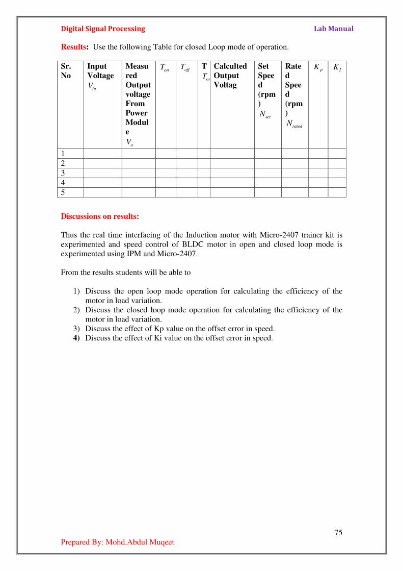
Digital Signal Processing Lab Manual
75
Prepared By: Mohd.Abdul Muqeet
Results: Use the following Table for closed Loop mode of operation.
Sr.
No
Input
Voltage
inV
Measu
red
Output
voltage
From
Power
Modul
e
oV
onT offT T
on offT T
Calculted
Output
Voltag
Set
Spee
d
(rpm
)
setN
Rate
d
Spee
d
(rpm
)
ratedN
pK
IK
1
2
3
4
5
Discussions on results:
Thus the real time interfacing of the Induction motor with Micro-2407 trainer kit is
experimented and speed control of BLDC motor in open and closed loop mode is
experimented using IPM and Micro-2407.
From the results students will be able to
1) Discuss the open loop mode operation for calculating the efficiency of the
motor in load variation.
2) Discuss the closed loop mode operation for calculating the efficiency of the
motor in load variation.
3) Discuss the effect of Kp value on the offset error in speed.
4) Discuss the effect of Ki value on the offset error in speed.
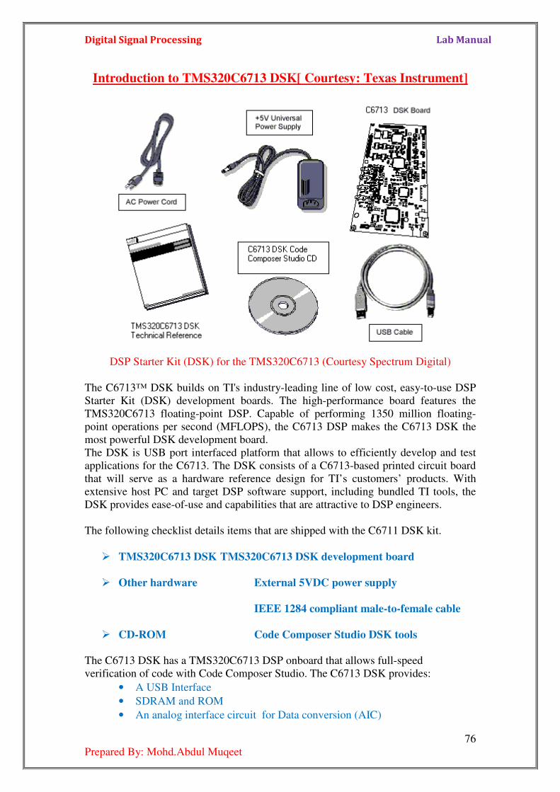
Digital Signal Processing Lab Manual
76
Prepared By: Mohd.Abdul Muqeet
Introduction to TMS320C6713 DSK[ Courtesy: Texas Instrument]
DSP Starter Kit (DSK) for the TMS320C6713 (Courtesy Spectrum Digital)
The C6713™ DSK builds on TI's industry-leading line of low cost, easy-to-use DSP
Starter Kit (DSK) development boards. The high-performance board features the
TMS320C6713 floating-point DSP. Capable of performing 1350 million floating-
point operations per second (MFLOPS), the C6713 DSP makes the C6713 DSK the
most powerful DSK development board.
The DSK is USB port interfaced platform that allows to efficiently develop and test
applications for the C6713. The DSK consists of a C6713-based printed circuit board
that will serve as a hardware reference design for TI’s customers’ products. With
extensive host PC and target DSP software support, including bundled TI tools, the
DSK provides ease-of-use and capabilities that are attractive to DSP engineers.
The following checklist details items that are shipped with the C6711 DSK kit.
TMS320C6713 DSK TMS320C6713 DSK development board
Other hardware External 5VDC power supply
IEEE 1284 compliant male-to-female cable
CD-ROM Code Composer Studio DSK tools
The C6713 DSK has a TMS320C6713 DSP onboard that allows full-speed
verification of code with Code Composer Studio. The C6713 DSK provides:
• A USB Interface
• SDRAM and ROM
• An analog interface circuit for Data conversion (AIC)

Digital Signal Processing Lab Manual
77
Prepared By: Mohd.Abdul Muqeet
• An I/O port
• Embedded JTAG emulation support
Connectors on the C6713 DSK provide DSP external memory interface (EMIF) and
peripheral signals that enable its functionality to be expanded with custom or third
party daughter boards.
The DSK provides a C6713 hardware reference design that can assist you in the
development of your own C6713-based products. In addition to providing a reference
for interfacing the DSP to various types of memories and peripherals, the design also
addresses power, clock, JTAG, and parallel peripheral interfaces.
The C6713 DSK includes a stereo codec. This analog interface circuit (AIC) has the
following characteristics:
High-Performance Stereo Codec
• 90-dB SNR Multibit Sigma-Delta ADC (A-weighted at 48 kHz)
• 100-dB SNR Multibit Sigma-Delta DAC (A-weighted at 48 kHz)
• 1.42 V – 3.6 V Core Digital Supply: Compatible With TI C54x DSP
Core Voltages
• 2.7 V – 3.6 V Buffer and Analog Supply: Compatible Both TI C54x
DSP Buffer Voltages
• 8-kHz – 96-kHz Sampling-Frequency Support
Software Control Via TI McBSP-Compatible Multiprotocol Serial Port
• I 2 C-Compatible and SPI-Compatible Serial-Port Protocols
• Glueless Interface to TI McBSPs
Audio-Data Input/Output Via TI McBSP-Compatible Programmable Audio Interface
• I 2 S-Compatible Interface Requiring Only One McBSP for both ADC
and DAC
• Standard I 2 S, MSB, or LSB Justified-Data Transfers
• 16/20/24/32-Bit Word Lengths
The C6713DSK has the following features:
The 6713 DSK is a low-cost standalone development platform that enables customers
to evaluate and develop applications for the TI C67XX DSP family. The DSK also
serves as a hardware reference design for the TMS320C6713 DSP. Schematics, logic
equations and application notes are available to ease hardware development and
reduce time to market.
The DSK uses the 32-bit EMIF for the SDRAM (CE0) and daughtercard expansion
interface (CE2 and CE3). The Flash is attached to CE1 of the EMIF in 8-bit mode.
An on-board AIC23 codec allows the DSP to transmit and receive analog signals.
McBSP0 is used for the codec control interface and McBSP1 is used for data. Analog
audio I/O is done through four 3.5mm audio jacks that correspond to microphone
input, line input, line output and headphone output. The codec can select the
microphone or the line input as the active input. The analog output is driven to both
Digital Signal Processing Lab Manual
78
Prepared By: Mohd.Abdul Muqeet
the line out (fixed gain) and headphone (adjustable gain) connectors. McBSP1 can be
re-routed to the expansion connectors in software.
A programmable logic device called a CPLD is used to implement glue logic that ties
the board components together. The CPLD has a register based user interface that lets
the user configure the board by reading and writing to the CPLD registers. The
registers reside at the midpoint of CE1.
The DSK includes 4 LEDs and 4 DIP switches as a simple way to provide the user
with interactive feedback. Both are accessed by reading and writing to the CPLD
registers.
An included 5V external power supply is used to power the board. On-board voltage
regulators provide the 1.26V DSP core voltage, 3.3V digital and 3.3V analog
voltages. A voltage supervisor monitors the internally generated voltage, and will
hold the board in reset until the supplies are within operating specifications and the
reset button is released. If desired, JP1 and JP2 can be used as power test points for
the core and I/O power supplies.
Code Composer communicates with the DSK through an embedded JTAG emulator
with a USB host interface. The DSK can also be used with an external emulator
through the external JTAG connector.
TMS320C6713 DSP Features
Highest-Performance Floating-Point Digital Signal Processor (DSP):
Eight 32-Bit Instructions/Cycle
32/64-Bit Data Word
300-, 225-, 200-MHz (GDP), and 225-, 200-, 167-MHz (PYP) Clock Rates
3.3-, 4.4-, 5-, 6-Instruction Cycle Times
2400/1800, 1800/1350, 1600/1200, and 1336/1000 MIPS /MFLOPS
Rich Peripheral Set, Optimized for Audio
Highly Optimized C/C++ Compiler
Extended Temperature Devices Available
Advanced Very Long Instruction Word (VLIW) TMS320C67x™ DSP Core
Eight Independent Functional Units:
Two ALUs (Fixed-Point)
Four ALUs (Floating- and Fixed-Point)
Two Multipliers (Floating- and Fixed-Point)
Load-Store Architecture With 32 32-Bit General-Purpose Registers
Instruction Packing Reduces Code Size
All Instructions Conditional
Instruction Set Features
Native Instructions for IEEE 754
Single- and Double-Precision
Byte-Addressable (8-, 16-, 32-Bit Data)
8-Bit Overflow Protection
Saturation; Bit-Field Extract, Set, Clear; Bit-Counting; Normalization
L1/L2 Memory Architecture
Digital Signal Processing
Prepared By: Mohd.Abdul Muqeet
4K-Byte L1P Program Cache (Direct
4K-Byte L1D Data Cache (2
256K-Byte L2 Memory Total: 64K
and 192K-Byte Additional L2 Mapped RAM
Device Configuration
Boot Mode: HPI, 8
Endianness: Little Endian, Big Endian
32-Bit External Memory Interface (EMIF)
Glueless Interface to SRAM, EPROM, Flash, SBSRAM, and SDRAM
512M-Byte Total Addressable External Memory Space
Enhanced Direct-Memory
16-Bit Host-Port Interface (HPI)
Two Multichannel Audio Serial Ports (McASPs)
Two Independent Clock Zones Each (1 TX and 1 RX)
Eight Serial Data Pins Per Port:
Individually Assignable to any of the C
Each Clock Zone Includes:
Programmable Clock Generator
Programmable Frame Sync Generator
TDM Streams From 2
Support for Slot Size:
8, 12, 16, 20, 24, 28, 32 Bits
Data Formatter for Bit Manipulation
Wide Variety of I2S and Similar Bit Stream Formats
Integrated Digital Audio Interface Transmitter (DIT) Supports:
S/PDIF, IEC60958
Up to 16 transmit pins
Enhanced Channel Status/User Data
Extensive Error Checking and Recovery
Two Inter-Integrated Circuit Bus (I2C Bus™) Multi
Two Multichannel Buffered Serial Ports:
Serial-Peripheral-Interface (SPI)
High-Speed TDM Interface
AC97 Interface
Two 32-Bit General-Purpose Timers
Dedicated GPIO Module With
Flexible Phase-Locked
IEEE-1149.1 (JTAG
Package Options:
208-Pin PowerPAD™ Plastic (Low
272-BGA Packages (GDP and
0.13-µm/6-Level Copper Metal Process
CMOS Technology
3.3-V I/Os, 1.2-V Internal (GDP & PYP)
3.3-V I/Os, 1.4-V Internal (GDP)(300 MHz only)
Prepared By: Mohd.Abdul Muqeet
Byte L1P Program Cache (Direct-Mapped)
Byte L1D Data Cache (2-Way)
Byte L2 Memory Total: 64K-Byte L2 Unified Cache/Mapped RAM,
Byte Additional L2 Mapped RAM
Boot Mode: HPI, 8-, 16-, 32-Bit ROM Boot
Endianness: Little Endian, Big Endian
Bit External Memory Interface (EMIF)
Glueless Interface to SRAM, EPROM, Flash, SBSRAM, and SDRAM
Byte Total Addressable External Memory Space
Memory-Access (EDMA) Controller (16 Independent Channels)
Port Interface (HPI)
Two Multichannel Audio Serial Ports (McASPs)
Two Independent Clock Zones Each (1 TX and 1 RX)
Eight Serial Data Pins Per Port:
Individually Assignable to any of the Clock Zones
Each Clock Zone Includes:
Programmable Clock Generator
Programmable Frame Sync Generator
TDM Streams From 2-32 Time Slots
Support for Slot Size:
8, 12, 16, 20, 24, 28, 32 Bits
Data Formatter for Bit Manipulation
Wide Variety of I2S and Similar Bit Stream Formats
Integrated Digital Audio Interface Transmitter (DIT) Supports:
S/PDIF, IEC60958-1, AES-3, CP-430 Formats
Up to 16 transmit pins
Enhanced Channel Status/User Data
Extensive Error Checking and Recovery
Integrated Circuit Bus (I2C Bus™) Multi-Master and Slave Interfaces
Two Multichannel Buffered Serial Ports:
Interface (SPI)
Speed TDM Interface
Purpose Timers
Dedicated GPIO Module With 16 pins (External Interrupt Capable)
Locked-Loop (PLL) Based Clock Generator Module
) Boundary-Scan-Compatible
Pin PowerPAD™ Plastic (Low-Profile) Quad Flatpack (PYP)
BGA Packages (GDP and ZDP)
Level Copper Metal Process
CMOS Technology
V Internal (GDP & PYP)
V Internal (GDP)(300 MHz only)
Lab Manual
79
Byte L2 Unified Cache/Mapped RAM,
Glueless Interface to SRAM, EPROM, Flash, SBSRAM, and SDRAM
ccess (EDMA) Controller (16 Independent Channels)
Integrated Digital Audio Interface Transmitter (DIT) Supports:
Master and Slave Interfaces
16 pins (External Interrupt Capable)
Loop (PLL) Based Clock Generator Module
Profile) Quad Flatpack (PYP)
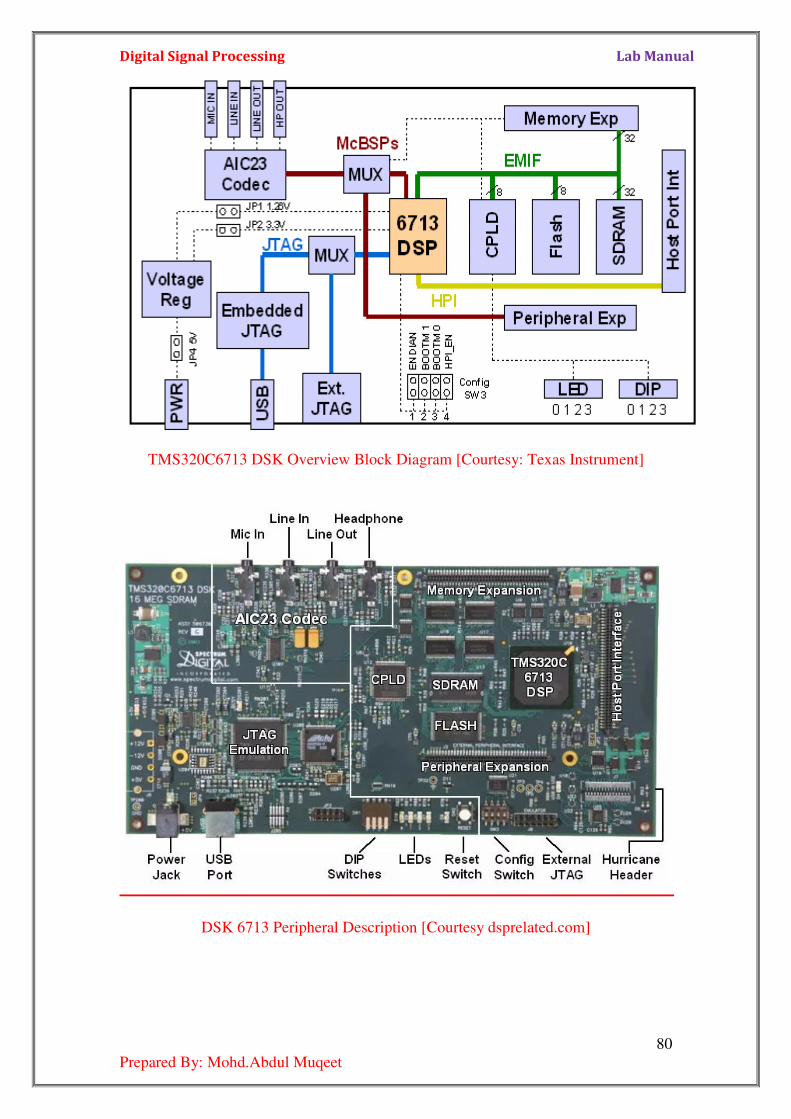
Digital Signal Processing Lab Manual
80
Prepared By: Mohd.Abdul Muqeet
TMS320C6713 DSK Overview Block Diagram [Courtesy: Texas Instrument]
DSK 6713 Peripheral Description [Courtesy dsprelated.com]
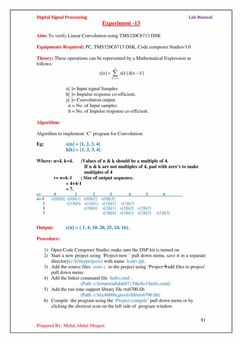
Digital Signal Processing Lab Manual
81
Prepared By: Mohd.Abdul Muqeet
Experiment -13
Aim: To verify Linear Convolution using TMS320C6713 DSK
Equipments Required: PC, TMS320C6713 DSK, Code composer Studiov3.0
Theory: These operations can be represented by a Mathematical Expression as
follows:
[ ] [ ]. [ ]k
y n x k h n k∞
=−∞
= −∑
x[ ]= Input signal Samples
h[ ]= Impulse response co-efficient.
y[ ]= Convolution output.
n = No. of Input samples
h = No. of Impulse response co-efficient.
Algorithm:
Algorithm to implement ‘C’ program for Convolution:
Eg: x[n] = 1, 2, 3, 4
h[k] = 1, 2, 3, 4
Where: n=4, k=4. ;Values of n & k should be a multiple of 4.
If n & k are not multiples of 4, pad with zero’s to make
multiples of 4
r= n+k-1 ; Size of output sequence.
= 4+4-1
= 7. r= 0 1 2 3 4 5 6 n= 0 x[0]h[0] x[0]h[1] x[0]h[2] x[0]h[3]
1 x[1]h[0] x[1]h[1] x[1]h[2] x[1]h[3]
2 x[2]h[0] x[2]h[1] x[2]h[2] x[2]h[3]
3 x[3]h[0] x[3]h[1] x[3]h[2] x[3]h[3]
Output: y[n] = 1, 4, 10, 20, 25, 24, 16.
Procedure:
1) Open Code Composer Studio; make sure the DSP kit is turned on.
2) Start a new project using ‘Project-new ‘ pull down menu, save it in a separate
directory(c:\ti\myprojects) with name lconv.pjt.
3) Add the source files conv.c to the project using ‘Projectadd files to project’
pull down menu.
4) Add the linker command file hello.cmd .
(Path: c:\ti\tutorial\dsk6713\hello1\hello.cmd)
5) Add the run time support library file rts6700.lib
(Path: c:\ti\c6000\cgtools\lib\rts6700.lib)
6) Compile the program using the ‘Project-compile’ pull down menu or by
clicking the shortcut icon on the left side of program window.
Digital Signal Processing Lab Manual
82
Prepared By: Mohd.Abdul Muqeet
7) Build the program using the ‘Project-Build’ pull down menu or by
clicking the shortcut icon on the left side of program window.
8) Load the program (lconv.out) in program memory of DSP chip using the
‘File-load program’ pull down menu.
9) To View output graphically
Select view graph time and frequency.
Program:
/* program to implement linear convolution */
#include<stdio.h>
#define LENGHT1 6 /*Lenght of i/p samples sequence*/
#define LENGHT2 4 /*Lenght of impulse response Co-
efficients */
int x[2*LENGHT1-1]=1,2,3,4,5,6,0,0,0,0,0; /*Input
Signal Samples*/
int h[2*LENGHT1-1]=1,2,3,4,0,0,0,0,0,0,0; /*Impulse
Response Co-efficients*/
int y[LENGHT1+LENGHT2-1];
main()
int i=0,j;
for(i=0;i<(LENGHT1+LENGHT2-1);i++)
y[i]=0;
for(j=0;j<=i;j++)
y[i]+=x[j]*h[i-j];
for(i=0;i<(LENGHT1+LENGHT2-1);i++)
printf("%d\n",y[i]);
Results:
Thus, the Linear Convolution of two given discrete sequence has been performed. The
input sequences are given in the program and the output will be displayed in the CCS
software.
Input x[n] = 1, 2, 3, 4
h[n] = 1, 2, 3, 4
Output: y[n] = 1, 4, 10, 20, 25, 24, 16.
Now configure the Graphical window as shown below
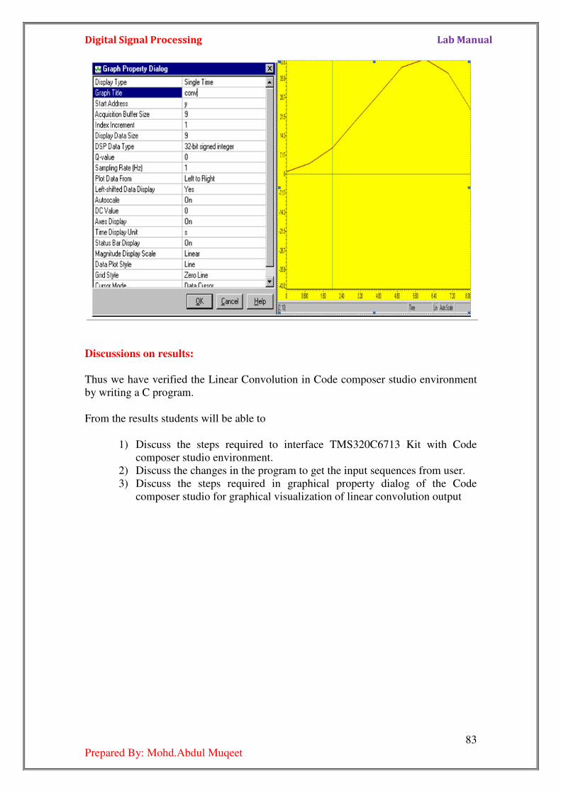
Digital Signal Processing Lab Manual
83
Prepared By: Mohd.Abdul Muqeet
Discussions on results:
Thus we have verified the Linear Convolution in Code composer studio environment
by writing a C program.
From the results students will be able to
1) Discuss the steps required to interface TMS320C6713 Kit with Code
composer studio environment.
2) Discuss the changes in the program to get the input sequences from user.
3) Discuss the steps required in graphical property dialog of the Code
composer studio for graphical visualization of linear convolution output
Digital Signal Processing Lab Manual
84
Prepared By: Mohd.Abdul Muqeet
Experiment -14
Aim: Generation of Sine wave and square wave using TMS320C6713 DSK and Code
Composer Studio.
Equipments Required: PC, TMS320C6713 DSK, Code composer Studiov3.0
Theory:
Sinusoidal Wave: The sine wave or sinusoidal wave is a mathematical curve that
describes smooth repetitive oscillations. It can be represented in mathematical form as
( ) sin ( )y t A t tω φ= + Where
A=Amplitude in V.
ω=angular frequency
ϕ=Phase in radins.
Square Wave: The square wave is a non sinusoidal periodic wave form which is
represented as infinite summation of sinusoidal waves in which the amplitude
alternates at a steady frequency between fixed minimum and maximum values with
the same duration at maximum and minimum.
Algorithm:
1) Define frequency in C program.
2) Generate the signals using corresponding general formula.
3) Plot the graph in Code Composer Studio.
Procedure for Sinusoidal wave form generation
1) Open Code Composer Studio; make sure the DSP kit is turned on.
2) Start a new project using ‘Project-new ‘ pull down menu, save it in a separate
directory(c:\ti\myprojects) with name lconv.pjt.
3) Add the source files sinewave.c to the project using ‘Projectadd files to
project’ pull down menu.
4) Add the linker command file hello.cmd .
(Path: c:\ti\tutorial\dsk6713\hello1\hello.cmd)
5) Add the run time support library file rts6700.lib
(Path: c:\ti\c6000\cgtools\lib\rts6700.lib)
6) Compile the program using the ‘Project-compile’ pull down menu or by
clicking the shortcut icon on the left side of program window.
7) Build the program using the ‘Project-Build’ pull down menu or by
clicking the shortcut icon on the left side of program window.
8) Load the program(sinewave.out) in program memory of DSP chip using the
‘File-load program’ pull down menu.
9) To View output graphically
Select view graph time and frequency.
Digital Signal Processing Lab Manual
85
Prepared By: Mohd.Abdul Muqeet
Program:
/* program for sinewave generation */
#include<stdio.h>
#include<math.h>
#define freq 400
float m[128];
main()
int n=0;
for(n=0;n<127;n++)
m[n]=sin(2*3.14*freq*n/24000)
printf(“%f”,m[n]);
Procedure for Square waveform generation
1) Open Code Composer Studio; make sure the DSP kit is turned on.
2) Start a new project using ‘Project-new ‘ pull down menu, save it in a separate
directory(c:\ti\myprojects) with name lconv.pjt.
3) Add the source files squarewave.c to the project using ‘Projectadd files to
project’ pull down menu.
4) Add the linker command file hello.cmd .
(Path: c:\ti\tutorial\dsk6713\hello1\hello.cmd)
5) Add the run time support library file rts6700.lib
(Path: c:\ti\c6000\cgtools\lib\rts6700.lib)
6) Compile the program using the ‘Project-compile’ pull down menu or by
clicking the shortcut icon on the left side of program window.
7) Build the program using the ‘Project-Build’ pull down menu or by
clicking the shortcut icon on the left side of program window.
8) Load the program(squarewave.out) in program memory of DSP chip using the
‘File-load program’ pull down menu.
9) To View output graphically
Select view graph time and frequency.
Program for Square wave Generation
/* program for Squarewave generation */
#include<stdio.h>
#include<math.h>
#define freq 500
float m[81];
main()
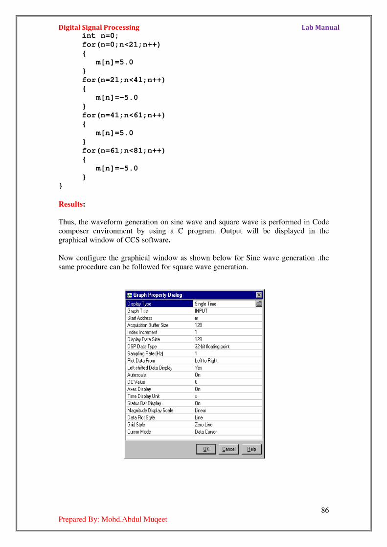
Digital Signal Processing Lab Manual
86
Prepared By: Mohd.Abdul Muqeet
int n=0;
for(n=0;n<21;n++)
m[n]=5.0
for(n=21;n<41;n++)
m[n]=-5.0
for(n=41;n<61;n++)
m[n]=5.0
for(n=61;n<81;n++)
m[n]=-5.0
Results:
Thus, the waveform generation on sine wave and square wave is performed in Code
composer environment by using a C program. Output will be displayed in the
graphical window of CCS software.
Now configure the graphical window as shown below for Sine wave generation .the
same procedure can be followed for square wave generation.

Digital Signal Processing Lab Manual
87
Prepared By: Mohd.Abdul Muqeet
Plot of sine waveform
Plot of Square wave form
Discussion on Results:
Thus we have performed the waveform generation in Code composer studio
environment by writing a C program.
From the results the student will be able to
1) Discuss the steps required to interface TMS320C6713 Kit with Code
composer studio environment.
2) Discuss the changes in the program to get the input sequences from user.
3) Discuss the steps required in graphical property dialog of the Code
composer studio for graphical visualization of the sine wave and square
wave output.
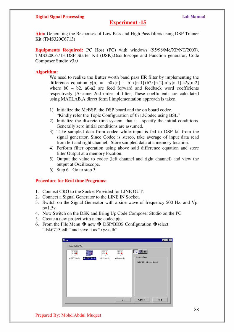
Digital Signal Processing Lab Manual
88
Prepared By: Mohd.Abdul Muqeet
Experiment -15 Aim: Generating the Responses of Low Pass and High Pass filters using DSP Trainer
Kit (TMS320C6713)
Equipments Required: PC Host (PC) with windows (95/98/Me/XP/NT/2000),
TMS320C6713 DSP Starter Kit (DSK).Oscilloscope and Function generator, Code
Composer Studio v3.0
Algorithm: We need to realize the Butter worth band pass IIR filter by implementing the
difference equation y[n] = b0x[n] + b1x[n-1]+b2x[n-2]-a1y[n-1]-a2y[n-2]
where b0 – b2, a0-a2 are feed forward and feedback word coefficients
respectively [Assume 2nd order of filter].These coefficients are calculated
using MATLAB.A direct form I implementation approach is taken.
1) Initialize the McBSP, the DSP board and the on board codec.
“Kindly refer the Topic Configuration of 6713Codec using BSL”
2) Initialize the discrete time system, that is , specify the initial conditions.
Generally zero initial conditions are assumed.
3) Take sampled data from codec while input is fed to DSP kit from the
signal generator. Since Codec is stereo, take average of input data read
from left and right channel. Store sampled data at a memory location.
4) Perform filter operation using above said difference equation and store
filter Output at a memory location.
5) Output the value to codec (left channel and right channel) and view the
output at Oscilloscope.
6) Step 6 - Go to step 3.
Procedure for Real time Programs:
1. Connect CRO to the Socket Provided for LINE OUT.
2. Connect a Signal Generator to the LINE IN Socket.
3. Switch on the Signal Generator with a sine wave of frequency 500 Hz. and Vp-
p=1.5v
4. Now Switch on the DSK and Bring Up Code Composer Studio on the PC.
5. Create a new project with name codec.pjt.
6. From the File Menu new DSP/BIOS Configuration select
“dsk6713.cdb” and save it as “xyz.cdb”
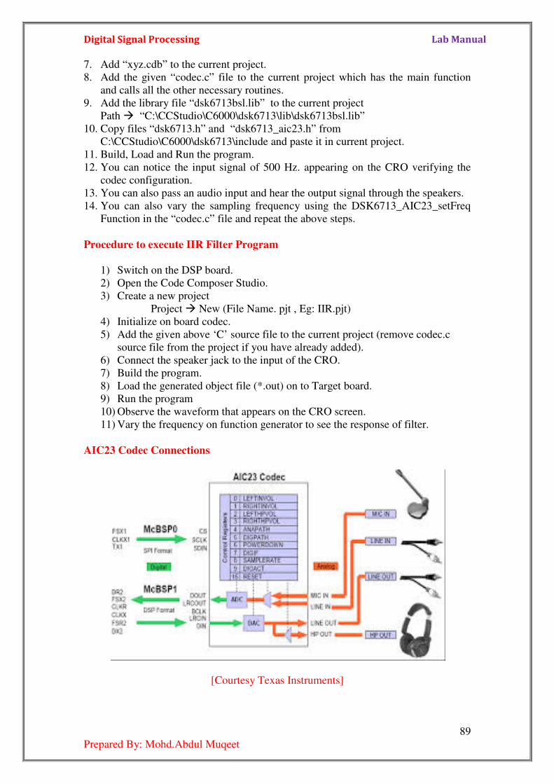
Digital Signal Processing Lab Manual
89
Prepared By: Mohd.Abdul Muqeet
7. Add “xyz.cdb” to the current project.
8. Add the given “codec.c” file to the current project which has the main function
and calls all the other necessary routines.
9. Add the library file “dsk6713bsl.lib” to the current project
Path “C:\CCStudio\C6000\dsk6713\lib\dsk6713bsl.lib”
10. Copy files “dsk6713.h” and “dsk6713_aic23.h” from
C:\CCStudio\C6000\dsk6713\include and paste it in current project.
11. Build, Load and Run the program.
12. You can notice the input signal of 500 Hz. appearing on the CRO verifying the
codec configuration.
13. You can also pass an audio input and hear the output signal through the speakers.
14. You can also vary the sampling frequency using the DSK6713_AIC23_setFreq
Function in the “codec.c” file and repeat the above steps.
Procedure to execute IIR Filter Program
1) Switch on the DSP board.
2) Open the Code Composer Studio.
3) Create a new project
Project New (File Name. pjt , Eg: IIR.pjt)
4) Initialize on board codec.
5) Add the given above ‘C’ source file to the current project (remove codec.c
source file from the project if you have already added).
6) Connect the speaker jack to the input of the CRO.
7) Build the program.
8) Load the generated object file (*.out) on to Target board.
9) Run the program
10) Observe the waveform that appears on the CRO screen.
11) Vary the frequency on function generator to see the response of filter.
AIC23 Codec Connections
[Courtesy Texas Instruments]
Digital Signal Processing Lab Manual
90
Prepared By: Mohd.Abdul Muqeet
Program:
#include "xyzcfg.h"
#include "dsk6713.h"
#include "dsk6713_aic23.h"
const signed int filter_Coeff[] =
//12730,-12730,12730,2767,-18324,21137 /*HP 2500 */
//312,312,312,32767,-27943,24367 /*LP 800 */
//1455,1455,1455,32767,-23140,21735 /*LP 2500 */
//9268,-9268,9268,32767,-7395,18367 /*HP 4000*/
7215,-7215,7215,32767,5039,6171, /*HP 7000*/
;
/* Codec configuration settings */
DSK6713_AIC23_Config config = \
0x0017, /* 0 DSK6713_AIC23_LEFTINVOL Left line input channel volume */
\ 0x0017, /* 1 DSK6713_AIC23_RIGHTINVOL Right line input channel volume
*/\
0x00d8, /* 2 DSK6713_AIC23_LEFTHPVOL Left channel headphone volume */
\
0x00d8, /* 3 DSK6713_AIC23_RIGHTHPVOL Right channel headphone volume */
\
0x0011, /* 4 DSK6713_AIC23_ANAPATH Analog audio path control */
\
0x0000, /* 5 DSK6713_AIC23_DIGPATH Digital audio path control */
\
0x0000, /* 6 DSK6713_AIC23_POWERDOWN Power down control */
\
0x0043, /* 7 DSK6713_AIC23_DIGIF Digital audio interface format */
\
0x0081, /* 8 DSK6713_AIC23_SAMPLERATE Sample rate control */
\
0x0001 /* 9 DSK6713_AIC23_DIGACT Digital interface activation */
\
;
/*
* main() - Main code routine, initializes BSL and generates tone
*/
void main()
DSK6713_AIC23_CodecHandle hCodec;
int l_input, r_input, l_output, r_output;
/* Initialize the board support library, must be called first */
DSK6713_init();
/* Start the codec */
hCodec = DSK6713_AIC23_openCodec(0, &config);
DSK6713_AIC23_setFreq(hCodec, 3);
while(1)
/* Read a sample to the left channel */
while (!DSK6713_AIC23_read(hCodec, &l_input));
/* Read a sample to the right channel */
while (!DSK6713_AIC23_read(hCodec, &r_input));
l_output=IIR_FILTER(&filter_Coeff ,l_input);
r_output=l_output;
/* Send a sample to the left channel */
Digital Signal Processing Lab Manual
91
Prepared By: Mohd.Abdul Muqeet
while (!DSK6713_AIC23_write(hCodec, l_output));
/* Send a sample to the right channel */
while (!DSK6713_AIC23_write(hCodec, r_output));
/* Close the codec */
DSK6713_AIC23_closeCodec(hCodec);
signed int IIR_FILTER(const signed int * h, signed int x1)
static signed int x[6] = 0, 0, 0, 0, 0, 0 ; /* x(n), x(n-1), x(n-
2). Must be static */
static signed int y[6] = 0, 0, 0, 0, 0, 0 ; /* y(n), y(n-1), y(n-
2). Must be static */
int temp=0;
temp = (short int)x1; /* Copy input to temp */
x[0] = (signed int) temp; /* Copy input to x[stages][0] */
temp = ( (int)h[0] * x[0]) ; /* B0 * x(n) */
temp += ( (int)h[1] * x[1]); /* B1/2 * x(n-1) */ temp += ( (int)h[1] * x[1]); /* B1/2 * x(n-1) */
temp += ( (int)h[2] * x[2]); /* B2 * x(n-2) */
temp -= ( (int)h[4] * y[1]); /* A1/2 * y(n-1) */
temp -= ( (int)h[4] * y[1]); /* A1/2 * y(n-1) */
temp -= ( (int)h[5] * y[2]); /* A2 * y(n-2) */
/* Divide temp by coefficients[A0] */
temp >>= 15;
if ( temp > 32767 )
temp = 32767;
else if ( temp < -32767)
temp = -32767;
y[0] = temp ;
/* Shuffle values along one place for next time */
y[2] = y[1]; /* y(n-2) = y(n-1) */ y[1] = y[0]; /* y(n-1) = y(n) */
x[2] = x[1]; /* x(n-2) = x(n-1) */
x[1] = x[0]; /* x(n-1) = x(n) */
/* temp is used as input next time through */
return (temp<<2);
Results:
Thus the result can be observer on the CRO for various frequencies.

Digital Signal Processing Lab Manual
92
Prepared By: Mohd.Abdul Muqeet
Discussions on results:
The designing of IIR Low pass and High Pass Filters requires initialization of BSL
codec.
From the results students will be able to
1) Discuss the real time interfacing of the TMS320C6713 Kit by using the
full functionality of the board support library files and AIC23 Codec.
2) Discuss the effect of changing the value of coefficients for filters.
3) Discuss the steps required to do the connection of CRO and function
generator to TMS320C6713 Kit.
Digital Signal Processing Lab Manual
93
Prepared By: Mohd.Abdul Muqeet
References
1. A.V Oppenheim,R.W. Schafer, “Digital Signal Processing”, Prentice Hall
Inc.1975.
2. John Proakis, Dimitris G Manolakis, “Digital Signal Processing Principles”,
Algorithms and Application”, PHI, 3rd Edition (1996).
3. S.K. Mitra, “Digital signal processing-A Computer based approach”, Tata
McGraw-Hill, 3rd Edition (2004).
4. S. Salivahana, A.Vallavaraj, Gnanapriya, “Digital Signal Processing”,
McGraw-Hill, 2nd
Edition (2000).
5. TMS320C6713 DSK with CCSv3.1 User Manual, Starcom Information
Technology Ltd.