Digital Logic Design - NTUpjcheng/course/asm2008/asm_ch2_dl.pdf · Digital Logic Design ... NAND...
102
Digital Logic Design B i Basics Combinational Circuits Sequential Circuits Pu-Jen Cheng Adapted from the slides prepared by S. Dandamudi for the book, Fundamentals of Computer Organization and Design.
Transcript of Digital Logic Design - NTUpjcheng/course/asm2008/asm_ch2_dl.pdf · Digital Logic Design ... NAND...

Digital Logic Design
B iBasicsCombinational CircuitsSequential Circuits
Pu-Jen Cheng
Adapted from the slides prepared by S. Dandamudi for the book, Fundamentals of Computer Organization and Design.

Introduction to Digital Logic Basics
Hardware consists of a few simple building blocksThese are called logic gates
AND, OR, NOT, … NAND, NOR, XOR, …
L i t b ilt i t i tLogic gates are built using transistorsNOT gate can be implemented by a single transistorAND gate requires 3 transistors
Transistors are the fundamental devicesPentium consists of 3 million transistorsCompaq Alpha consists of 9 million transistorsNow we can build chips with more than 100 million transistors
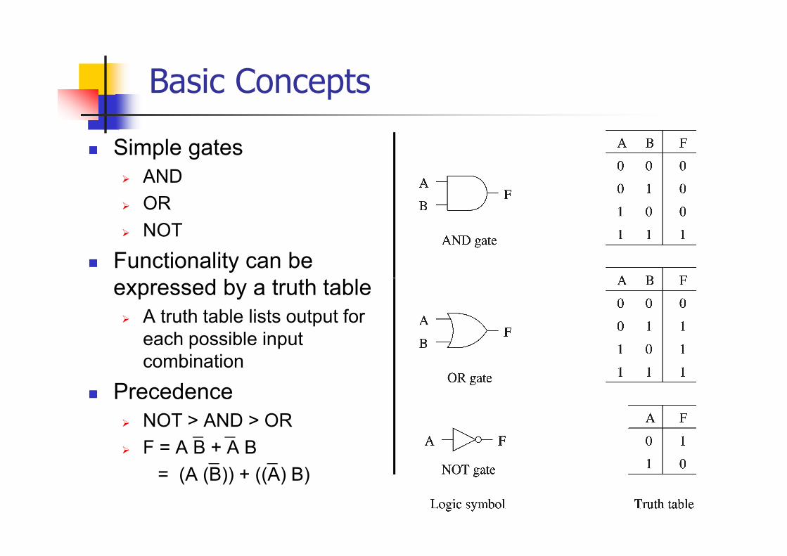
Basic Concepts
Simple gatesANDORNOT
Functionality can be expressed by a truth table
A truth table lists output for each possible input combination
PrecedenceNOT > AND > ORF = A B + A B
= (A (B)) + ((A) B)
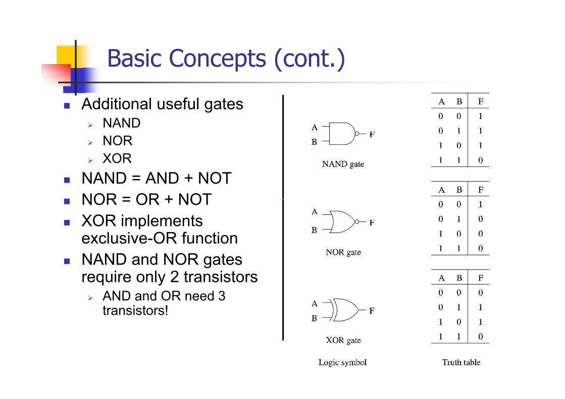
Basic Concepts (cont.)
Additional useful gatesNANDNORXOR
NAND = AND + NOTNOR = OR + NOTNOR = OR + NOTXOR implements exclusive-OR functionNAND and NOR gates require only 2 transistors
AND and OR need 3 transistors!
Basic Concepts (cont.)
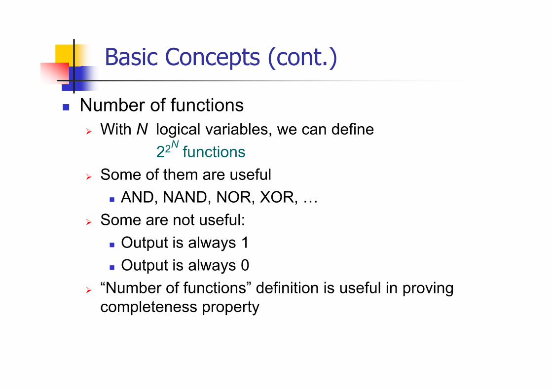
Number of functionsWith N logical variables, we can define
22N functionsSome of them are useful
AND NAND NOR XORAND, NAND, NOR, XOR, …Some are not useful:
Output is always 1Output is always 0
“Number of functions” definition is useful in proving completeness property

Basic Concepts (cont.)
Complete setsA set of gates is complete
If we can implement any logical function using only the type of gates in the set
You can uses as many gates as you wantSome example complete setsSome example complete sets
{AND, OR, NOT} Not a minimal complete set{AND, NOT}{OR, NOT}{NAND}{NOR}
Minimal complete setA complete set with no redundant elements.

Basic Concepts (cont.)
Proving NAND gate is universalNAND gate is called universal gate

Basic Concepts (cont.)
Proving NOR gate is universalNOR gate is called universal gate

Logic Chips
Logic Chips (cont.)
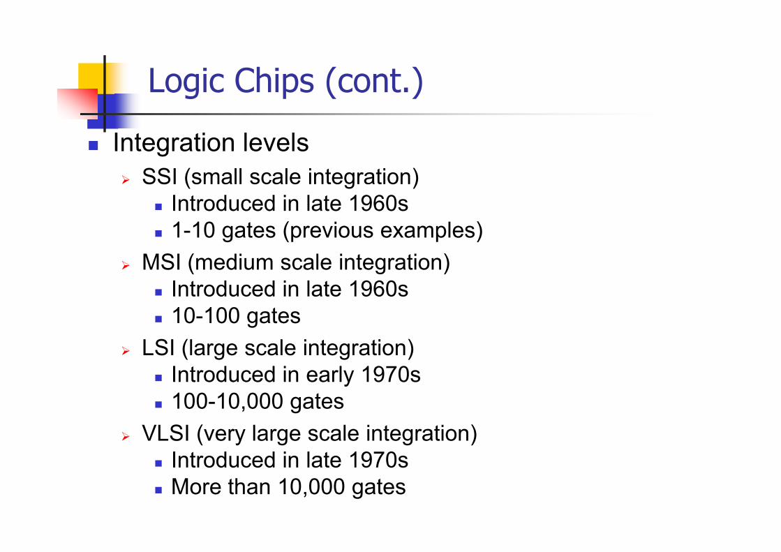
Integration levelsSSI (small scale integration)
Introduced in late 1960s1-10 gates (previous examples)
MSI (medium scale integration)Introduced in late 1960s10-100 gates
LSI (large scale integration)Introduced in early 1970s100-10,000 gates
VLSI (very large scale integration)Introduced in late 1970sMore than 10,000 gates

Logic Functions
Logical functions can be expressed in several ways:
Truth tableLogical expressionsGraphical formGraphical form
Example:Majority function
Output is 1 whenever majority of inputs is 1We use 3-input majority function

Logic Functions (cont.)
3-input majority function
A B C F0 0 0 00 0 1 0
Logical expression formF = A B + B C + A C
0 1 0 00 1 1 11 0 0 01 0 1 11 1 0 11 1 1 1

Logical Equivalence
All three circuits implement F = A B function

Logical Equivalence (cont.)
Proving logical equivalence of two circuitsDerive the logical expression for the output of each circuitShow that these two expressions are equivalent
Two ways:Two ways:You can use the truth table method
For every combination of inputs, if both expressions yield the same output, they are equivalentGood for logical expressions with small number of variables
You can also use algebraic manipulationNeed Boolean identities
Logical Equivalence (cont.)
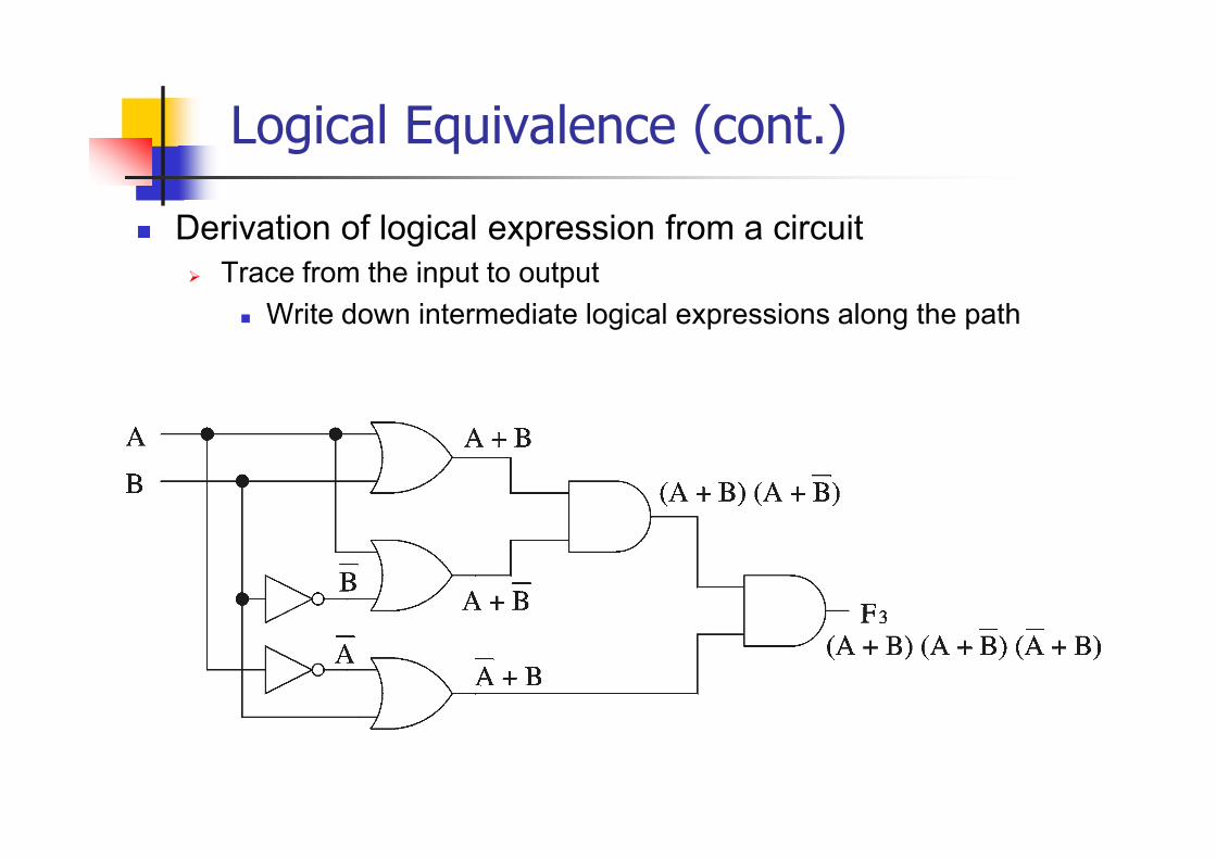
Derivation of logical expression from a circuitTrace from the input to output
Write down intermediate logical expressions along the path
Logical Equivalence (cont.)
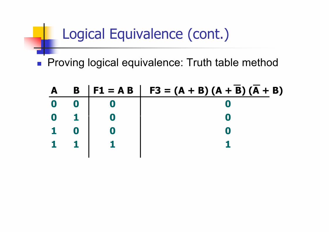
Proving logical equivalence: Truth table method
A B F1 = A B F3 = (A + B) (A + B) (A + B)0 0 0 00 1 0 00 1 0 01 0 0 01 1 1 1
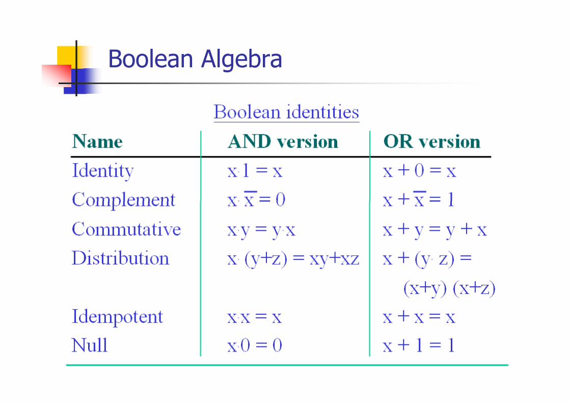
Boolean Algebra

Boolean Algebra (cont.)
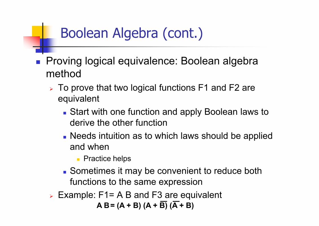
Boolean Algebra (cont.)
Proving logical equivalence: Boolean algebra method
To prove that two logical functions F1 and F2 are equivalent
Start with one function and apply Boolean laws toStart with one function and apply Boolean laws to derive the other functionNeeds intuition as to which laws should be applied and when
Practice helps
Sometimes it may be convenient to reduce both functions to the same expression
Example: F1= A B and F3 are equivalentA B= (A + B) (A + B) (A + B)
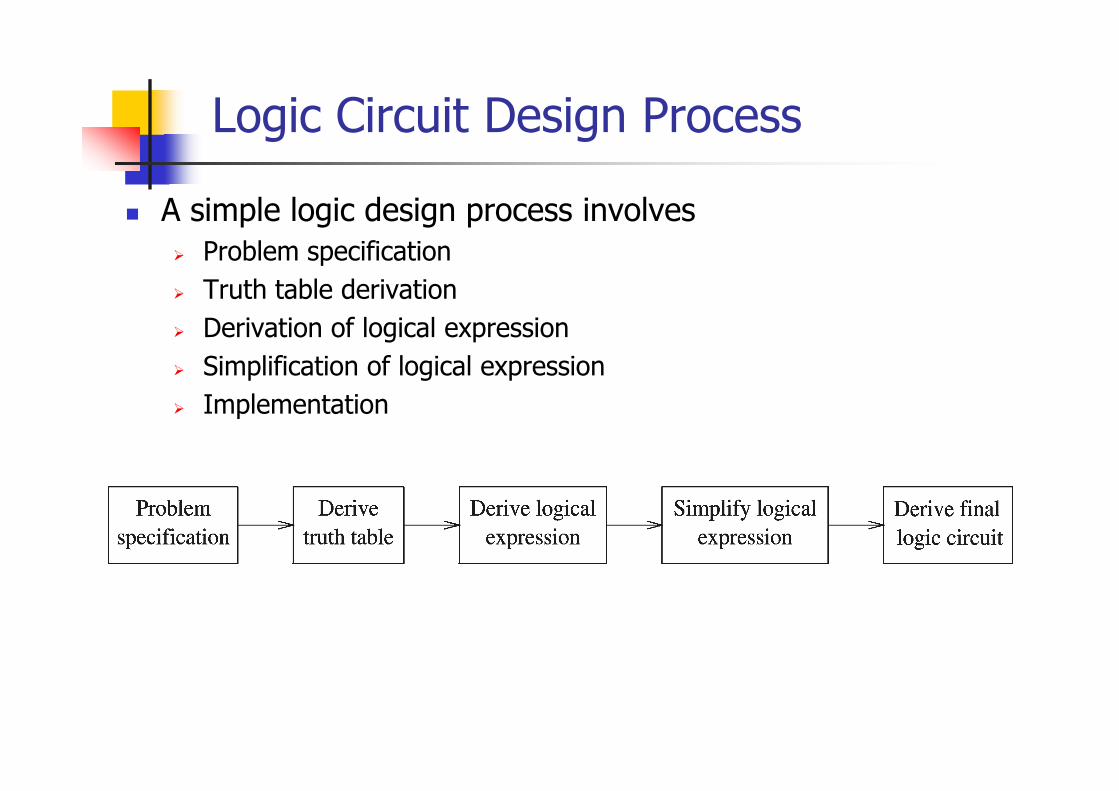
Logic Circuit Design Process
A simple logic design process involvesProblem specificationTruth table derivationDerivation of logical expressionSimplification of logical expressionI l t tiImplementation

Deriving Logical Expressions
Derivation of logical expressions from truth tablessum-of-products (SOP) formproduct-of-sums (POS) form
SOP form W i AND f h i bi i hWrite an AND term for each input combination that produces a 1 output
Write the variable if its value is 1; complement otherwise
OR the AND terms to get the final expressionPOS form
Dual of the SOP form
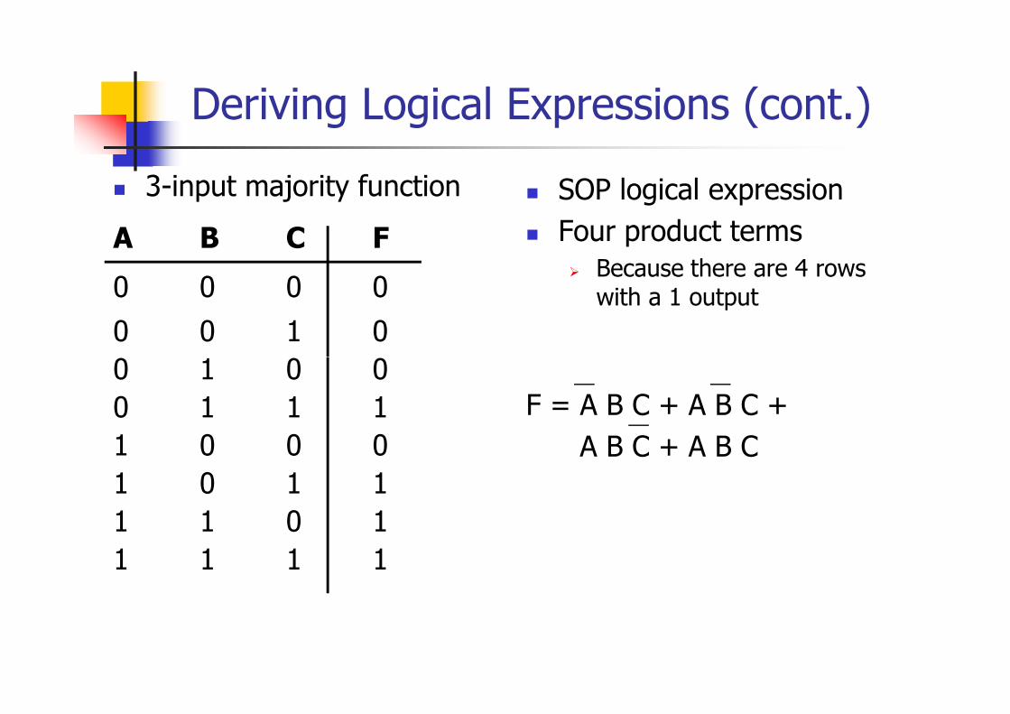
Deriving Logical Expressions (cont.)
3-input majority function
A B C F
0 0 0 00 0 1 0
SOP logical expressionFour product terms
Because there are 4 rows with a 1 output
0 1 0 00 1 1 11 0 0 01 0 1 11 1 0 11 1 1 1
F = A B C + A B C + A B C + A B C

Deriving Logical Expressions (cont.)
3-input majority function
A B C F
0 0 0 00 0 1 0
POS logical expressionFour sum terms
Because there are 4 rows with a 0 output
0 1 0 00 1 1 11 0 0 01 0 1 11 1 0 11 1 1 1
F = (A + B + C) (A + B + C)(A + B + C) (A + B + C)
Logical Expression Simplification
Two basic methodsAlgebraic manipulation
Use Boolean laws to simplify the expressionDifficult to useDon’t know if you have the simplified form
Karnaugh map (K-map) methodKarnaugh map (K-map) methodGraphical methodEasy to use
Can be used to simplify logical expressions with a few variables

Algebraic Manipulation
Majority function example
A B C + A B C + A B C + A B C =
A B C + A B C + A B C + A B C + A B C + A B C
Added extra
We can now simplify this expression as
B C + A C + A B
A difficult method to use for complex expressions

Karnaugh Map Method
Note the order

Karnaugh Map Method (cont.)
Simplification examples
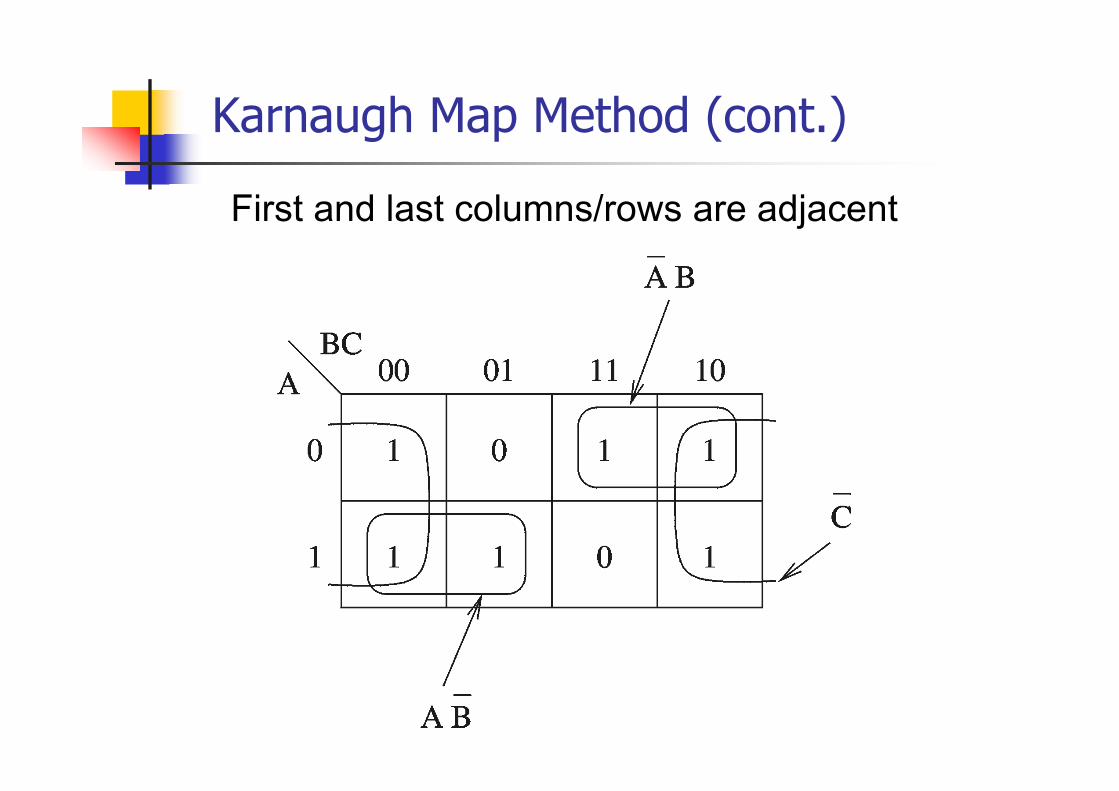
Karnaugh Map Method (cont.)
First and last columns/rows are adjacent
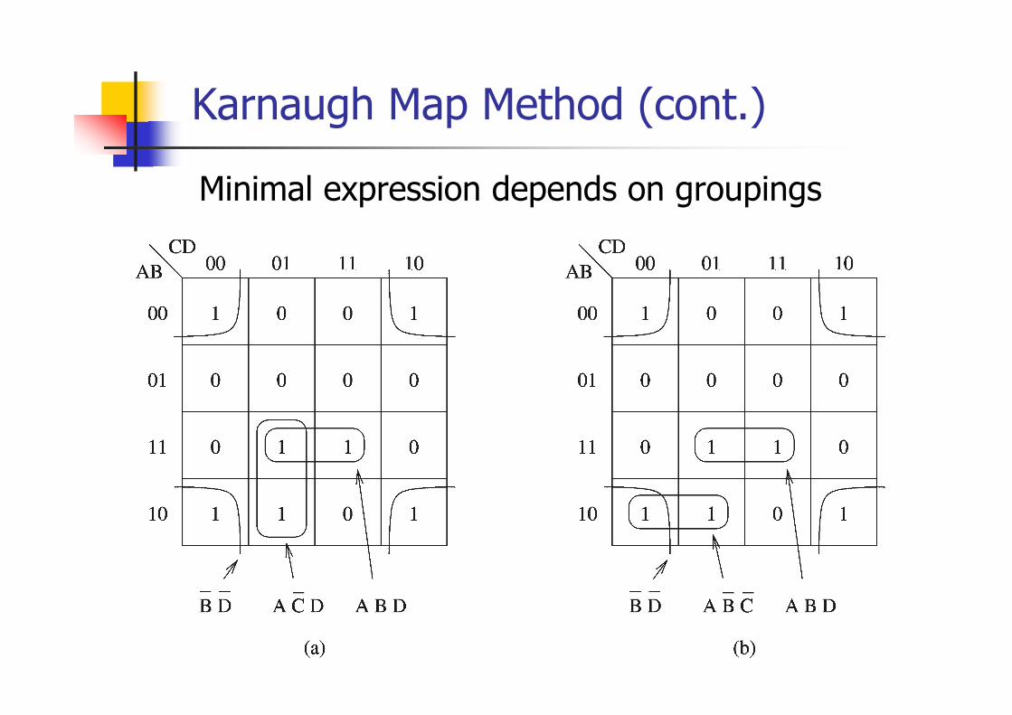
Karnaugh Map Method (cont.)
Minimal expression depends on groupings
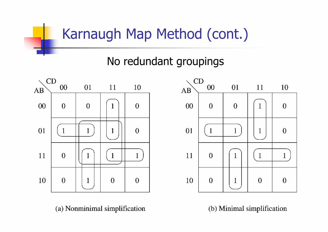
Karnaugh Map Method (cont.)
No redundant groupings
Karnaugh Map Method (cont.)
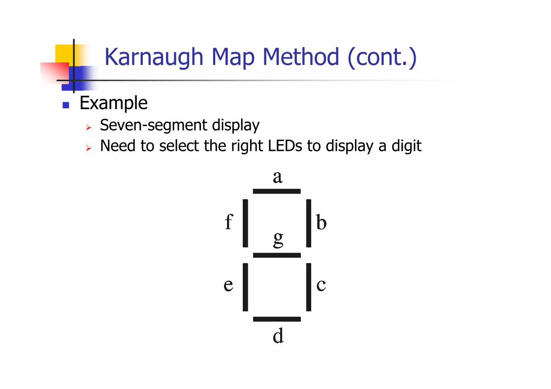
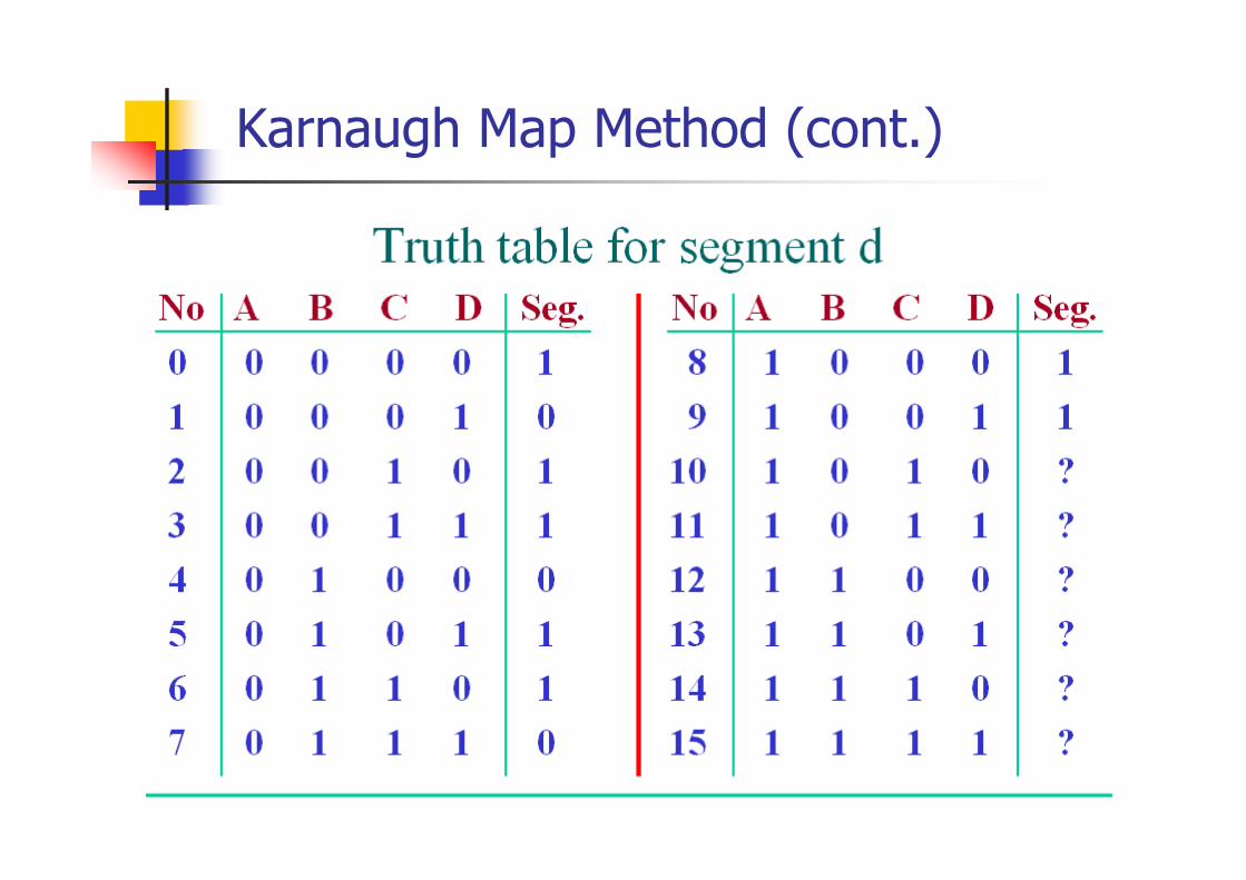
ExampleSeven-segment displayNeed to select the right LEDs to display a digit
Karnaugh Map Method (cont.)
Karnaugh Map Method (cont.)
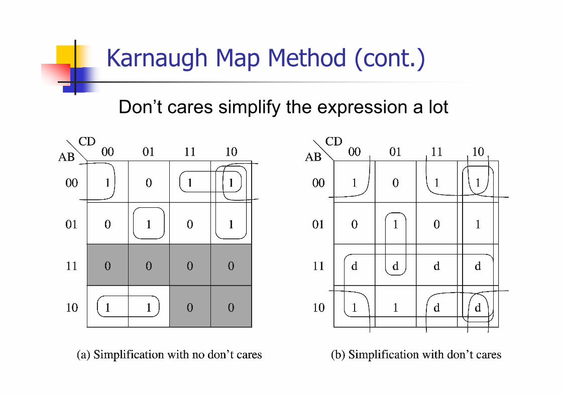
Don’t cares simplify the expression a lot

Implementation Using NAND Gates
Using NAND gatesGet an equivalent expression
A B + C D = A B + C DUsing de Morgan’s lawU g d o ga a
A B + C D = A B . C DCan be generalized
Majority function
A B + B C + AC = A B . BC . AC
Idea: NAND Gates: Sum-of-Products, NOR Gates: Product-of-Sums

Implementation Using NAND Gates (cont.)
Majority function

Introduction to Combinational Circuits
Combinational circuitsOutput depends only on the current inputs
Combinational circuits provide a higher level of abstraction
H l i d i d i l itHelp in reducing design complexityReduce chip count
We look at some useful combinational circuits
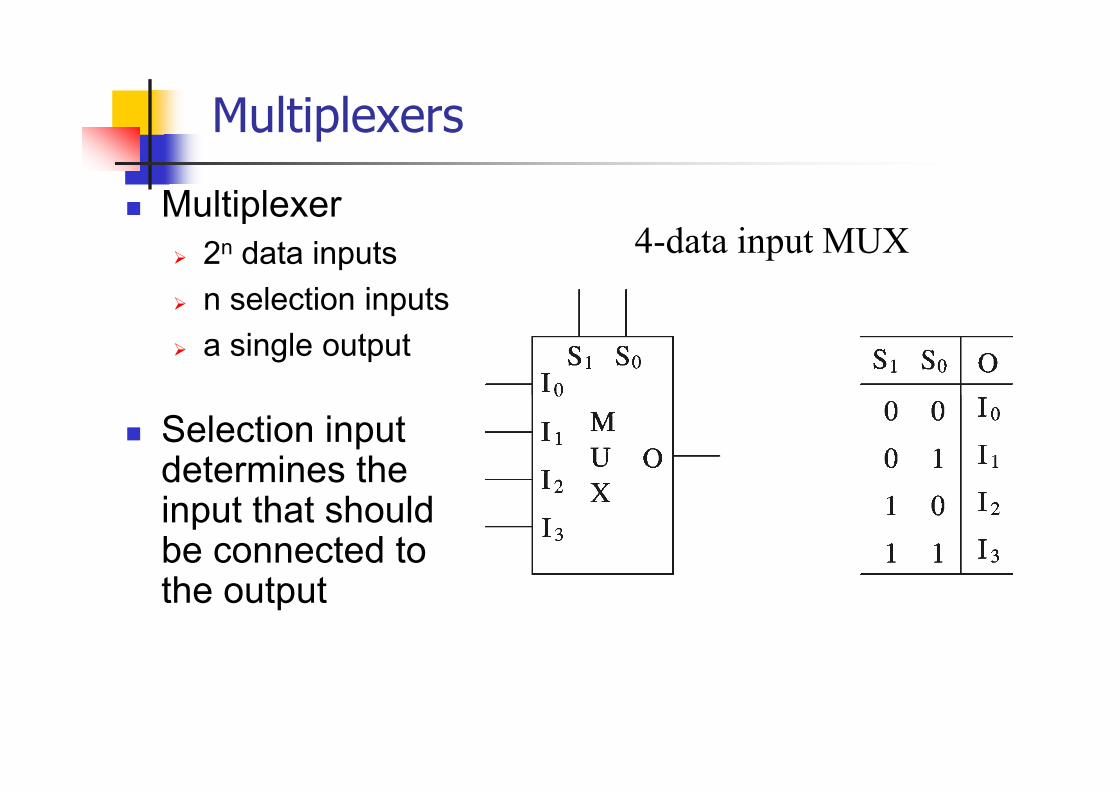
Multiplexers
Multiplexer2n data inputsn selection inputsa single output
4-data input MUX
Selection input determines the input that should be connected to the output

Multiplexers (cont.)
4-data input MUX implementation
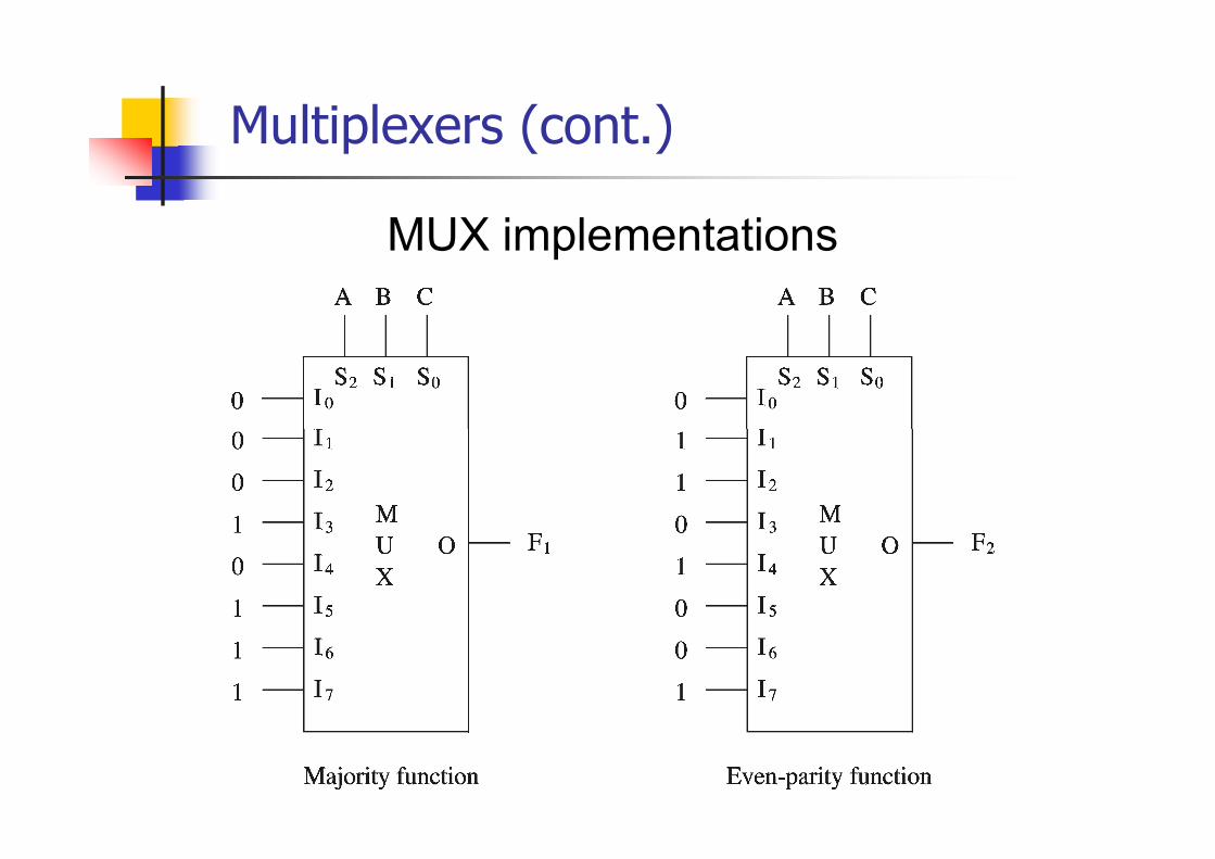
Multiplexers (cont.)
MUX implementations
Multiplexers (cont.)
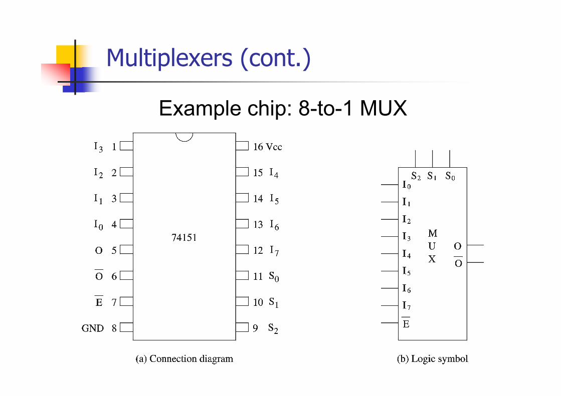
Example chip: 8-to-1 MUX
Multiplexers (cont.)
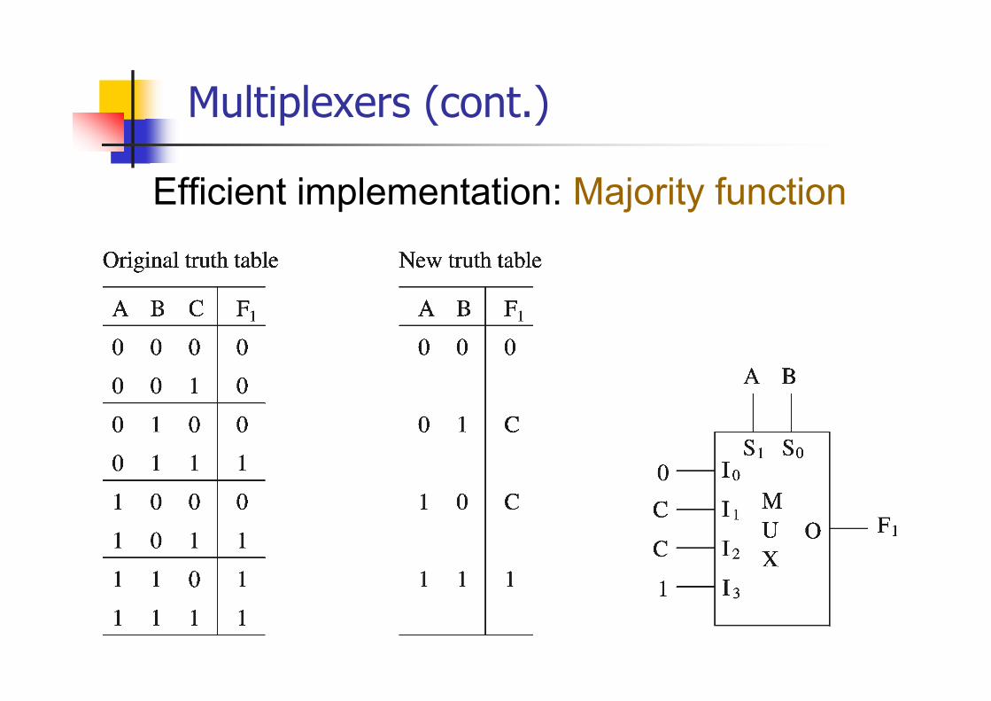
Efficient implementation: Majority function
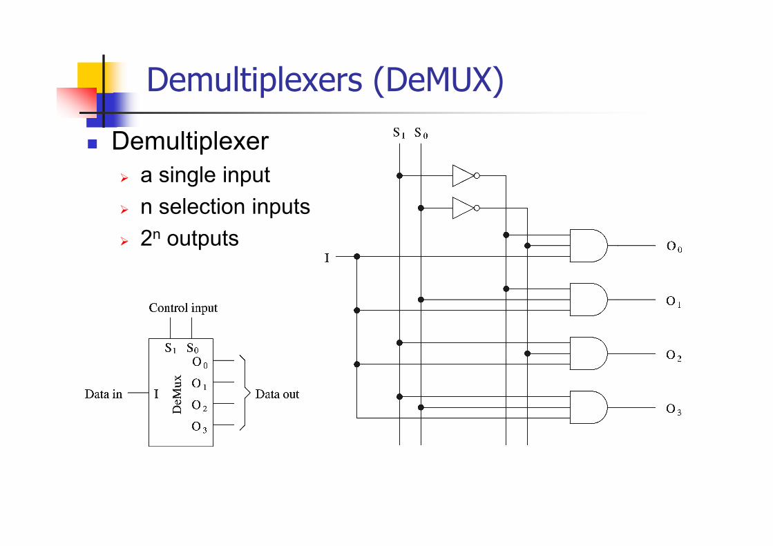
Demultiplexers (DeMUX)
Demultiplexera single inputn selection inputs2n outputs
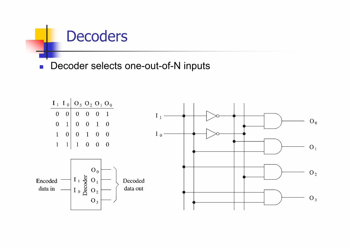
Decoders
Decoder selects one-out-of-N inputs

Decoders (cont.)
Logic function implementation
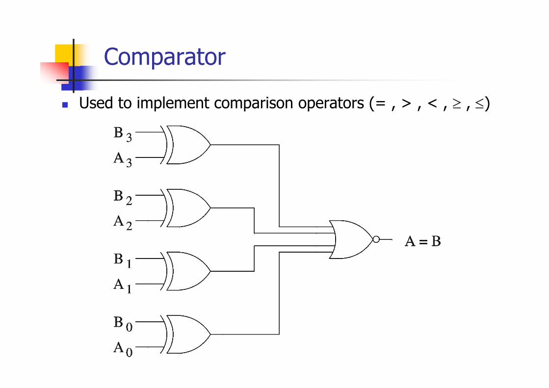
Comparator
Used to implement comparison operators (= , > , < , ≥ , ≤)
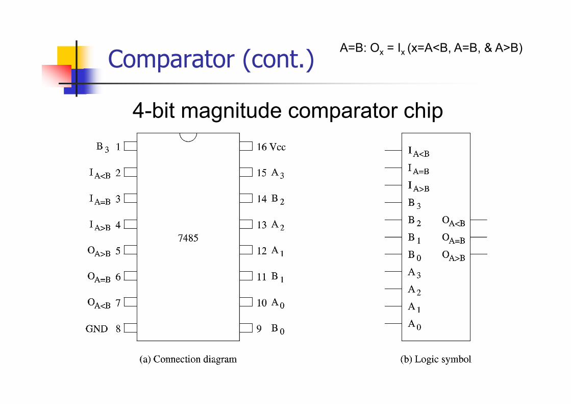
Comparator (cont.)
4-bit magnitude comparator chip
A=B: Ox = Ix (x=A<B, A=B, & A>B)

Comparator (cont.)
Serial construction of an 8-bit comparator

1-bit Comparator
x y
x>y
x=yx<y
CMP
x y x>y x=y x<y

8-bit comparator
x y
x>y
x=yx<y
CMP
xn>yn
xn=yn
xn<yn
x y
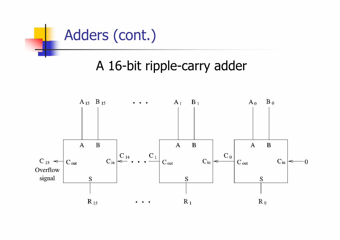
Adders
Half-adderAdds two bits
Produces a sum and carryProblem: Cannot use it to build larger inputs
F ll ddFull-adderAdds three 1-bit values
Like half-adder, produces a sum and carryAllows building N-bit adders
Simple techniqueConnect Cout of one adder to Cin of the next
These are called ripple-carry adders

Adders (cont.)
Adders (cont.)
A 16-bit ripple-carry adder

Adders (cont.)
Ripple-carry adders can be slowDelay proportional to number of bits
Carry lookahead addersEliminate the delay of ripple-carry addersCarry-ins are generated independentlyCarry ins are generated independently
C0 = A0 B0C1 = A0 B0 A1 + A0 B0 B1 + A1 B1
. . .Requires complex circuitsUsually, a combination carry lookahead and ripple-carry techniques are used
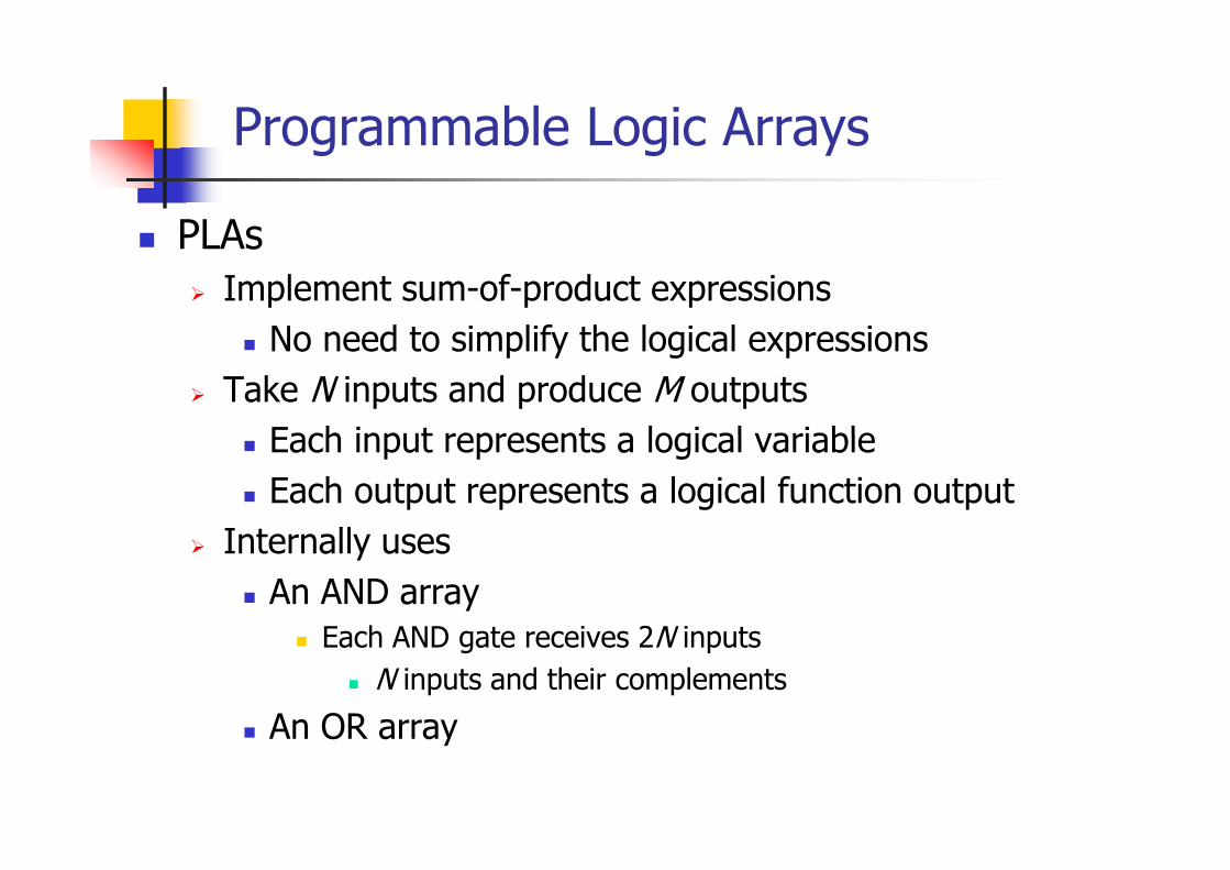
Programmable Logic Arrays
PLAsImplement sum-of-product expressions
No need to simplify the logical expressionsTake N inputs and produce M outputs
Each input represents a logical variableEach input represents a logical variableEach output represents a logical function output
Internally usesAn AND array
Each AND gate receives 2N inputsN inputs and their complements
An OR array
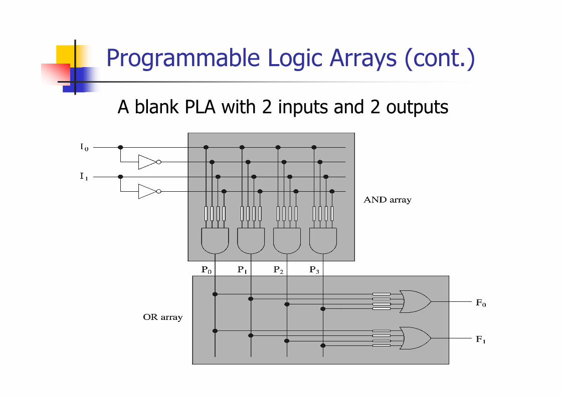
Programmable Logic Arrays (cont.)
A blank PLA with 2 inputs and 2 outputs

Programmable Logic Arrays (cont.)
Implementation examples
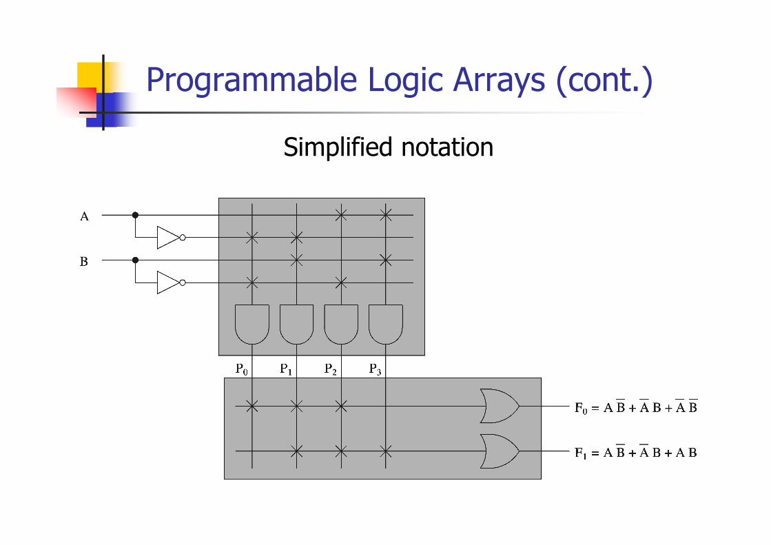
Programmable Logic Arrays (cont.)
Simplified notation
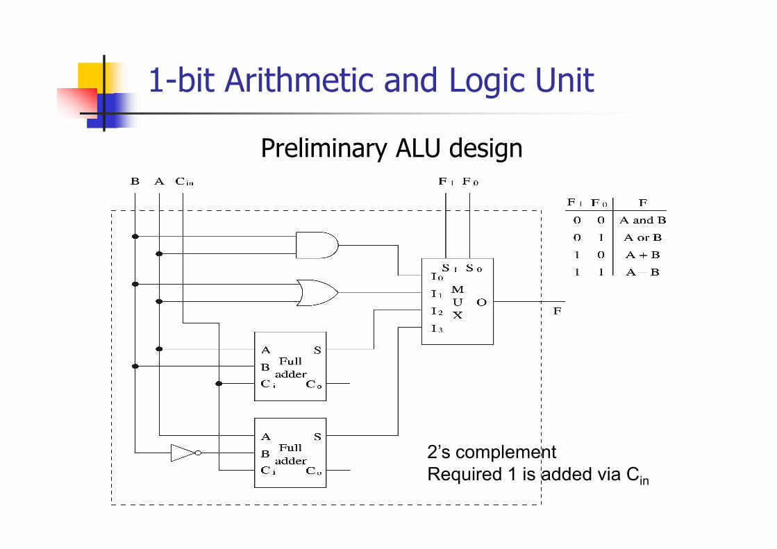
1-bit Arithmetic and Logic Unit
Preliminary ALU design
2’s complementRequired 1 is added via Cin

1-bit Arithmetic and Logic Unit (cont.)
Final design
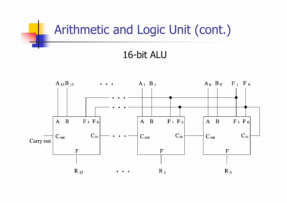
Arithmetic and Logic Unit (cont.)
16-bit ALU

Arithmetic and Logic Unit (cont’d)
4-bit ALU
Introduction to Sequential Circuits
Output depends on current as well as past inputsDepends on the historyHave “memory” property
Sequential circuit consists of C bi i l i iCombinational circuitFeedback circuit
Past input is encoded into a set of state variablesUses feedback (to feed the state variables)
Simple feedbackUses flip flops

Introduction (cont.)
Main components of a sequential circuit
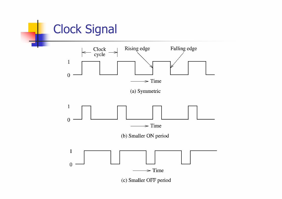
Clock Signal

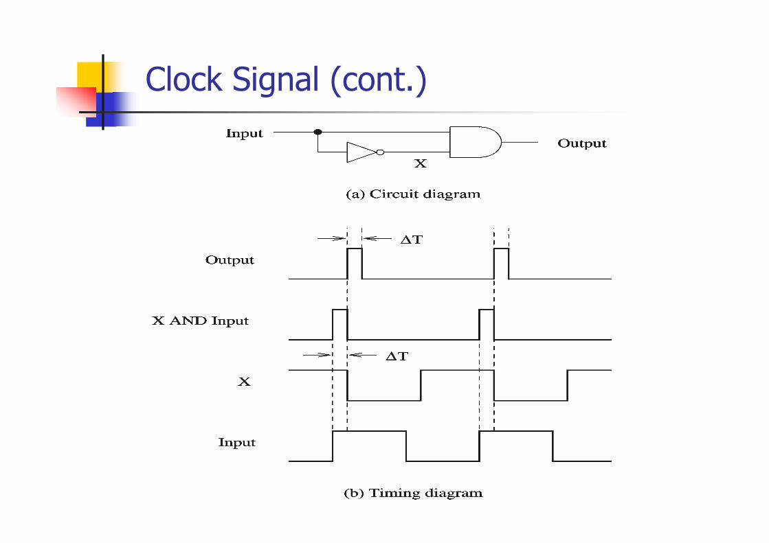
Clock Signal (cont.)
Clock serves two distinct purposesSynchronization point
Start of a cycleEnd of a cycleIntermediate point at which the clock signal changesIntermediate point at which the clock signal changes levels
Timing informationClock period, ON, and OFF periods
Propagation delayTime required for the output to react to changes in the inputs
Clock Signal (cont.)
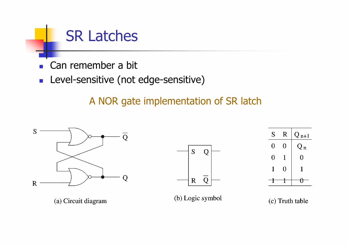
SR Latches
Can remember a bitLevel-sensitive (not edge-sensitive)
A NOR gate implementation of SR latch
SR Latches (cont.)
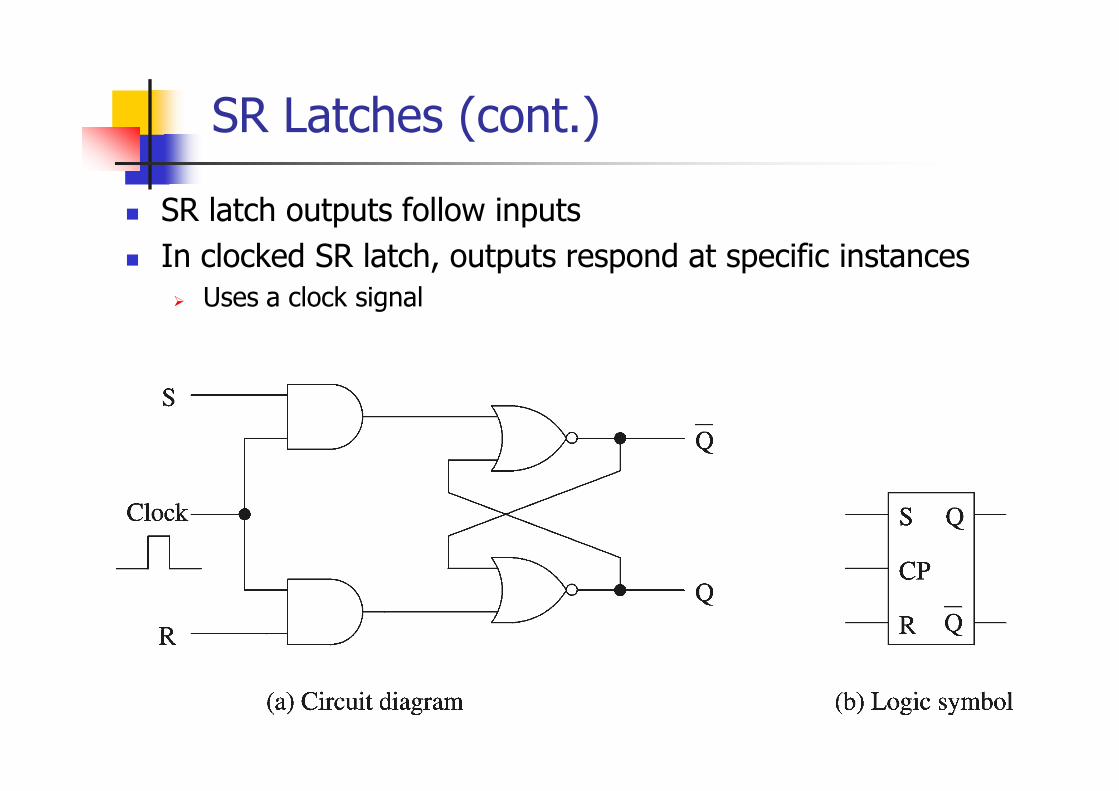
SR latch outputs follow inputsIn clocked SR latch, outputs respond at specific instances
Uses a clock signal

D Latches
D LatchAvoids the SR = 11 state
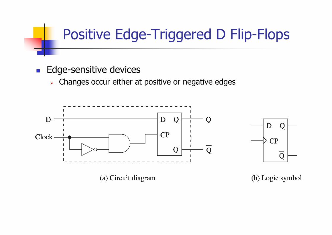
Positive Edge-Triggered D Flip-Flops
Edge-sensitive devicesChanges occur either at positive or negative edges

Notation for Latches & Flip-Flops
Not strictly followed in the literature
Latches Flip-flops
Low level High level Positive edge Negative edge

Example of Shift Register Using D Flip-Flops
74164 shift
Register chip
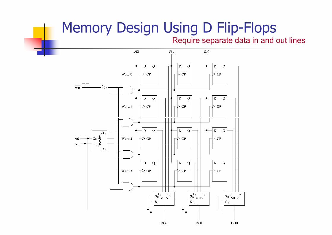
Memory Design Using D Flip-FlopsRequire separate data in and out lines
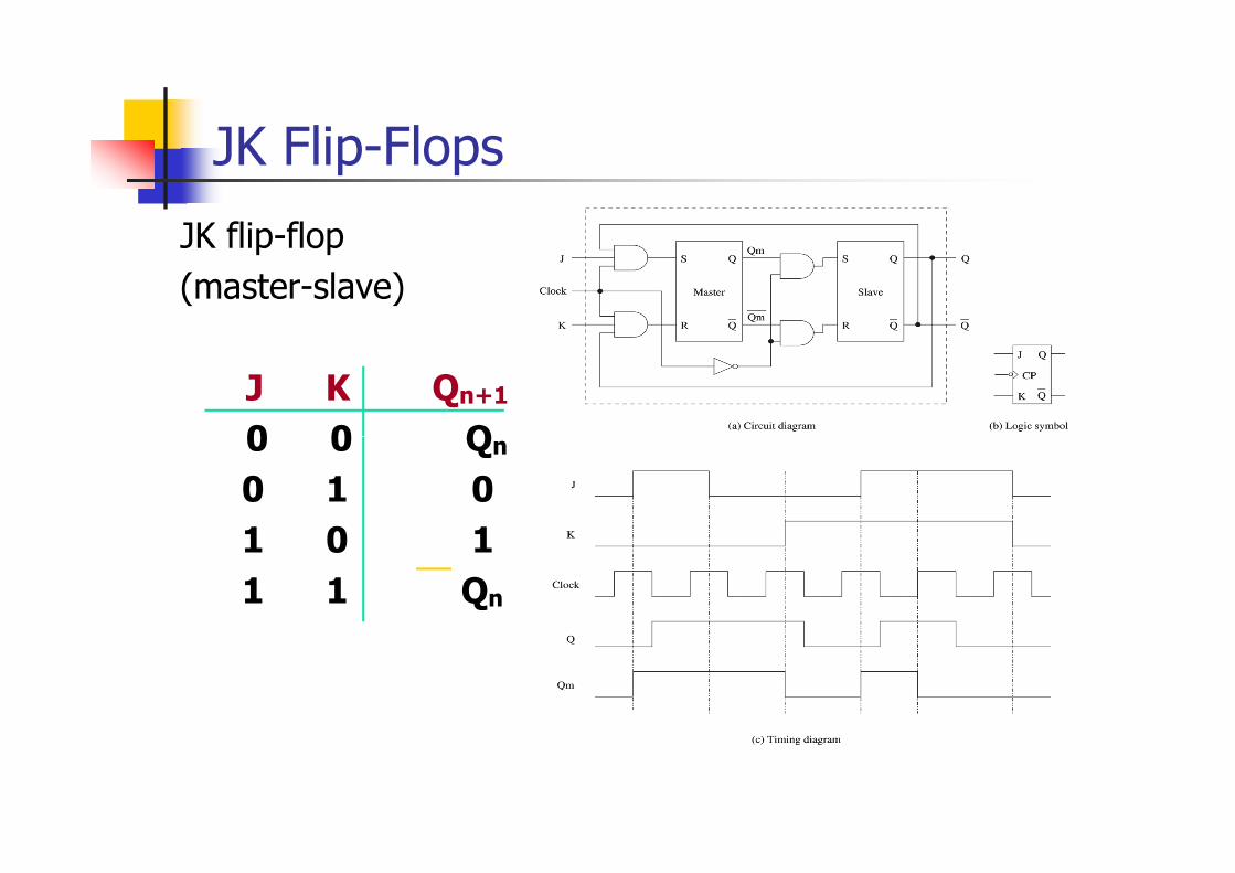
JK Flip-Flops
JK flip-flop (master-slave)
J K Qn+1
0 0 Q0 0 Qn
0 1 01 0 11 1 Qn
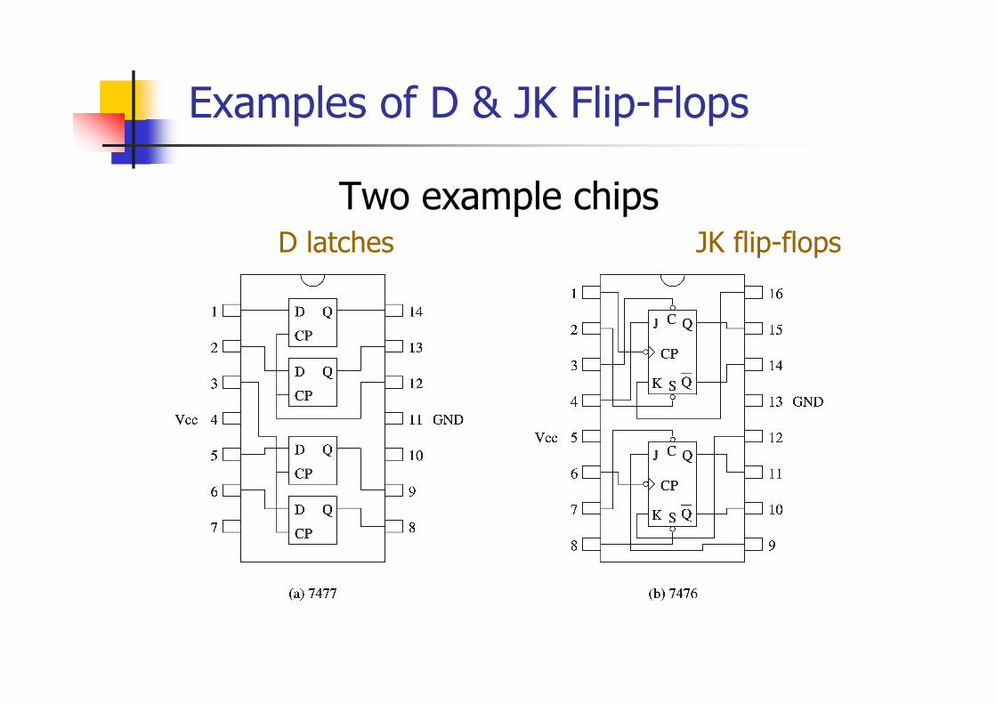
Examples of D & JK Flip-Flops
Two example chipsD latches JK flip-flops
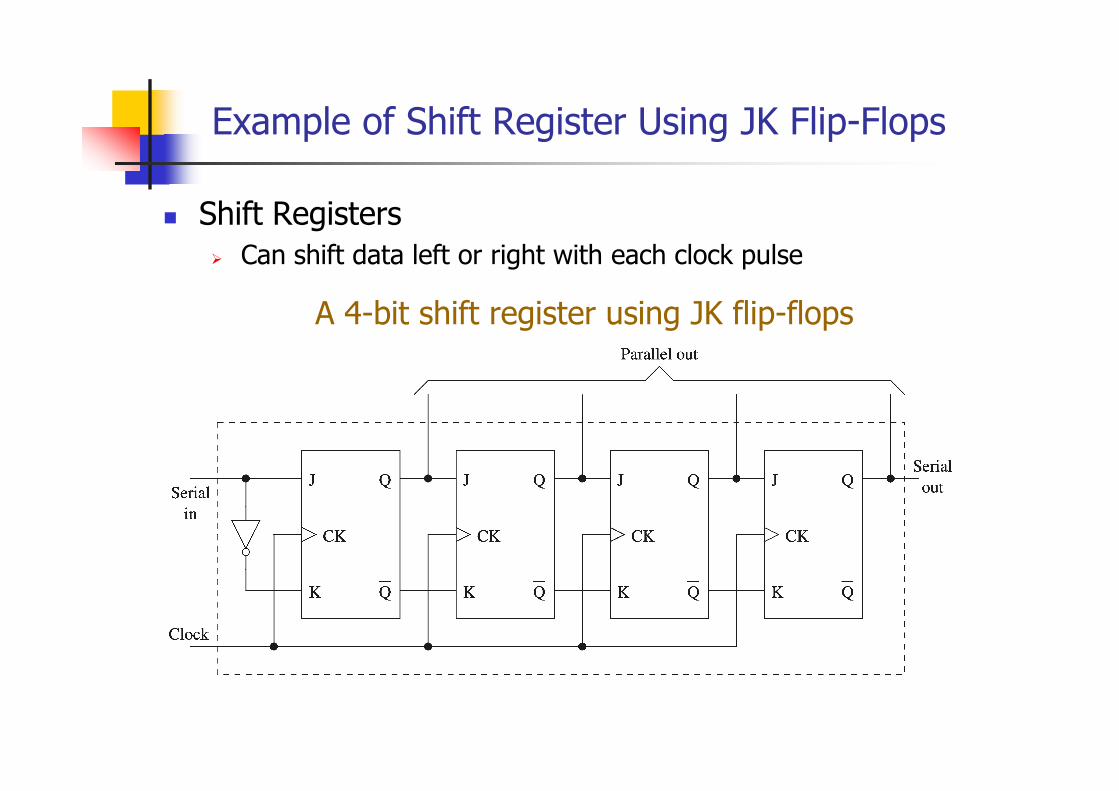
Example of Shift Register Using JK Flip-Flops
Shift RegistersCan shift data left or right with each clock pulse
A 4-bit shift register using JK flip-flops
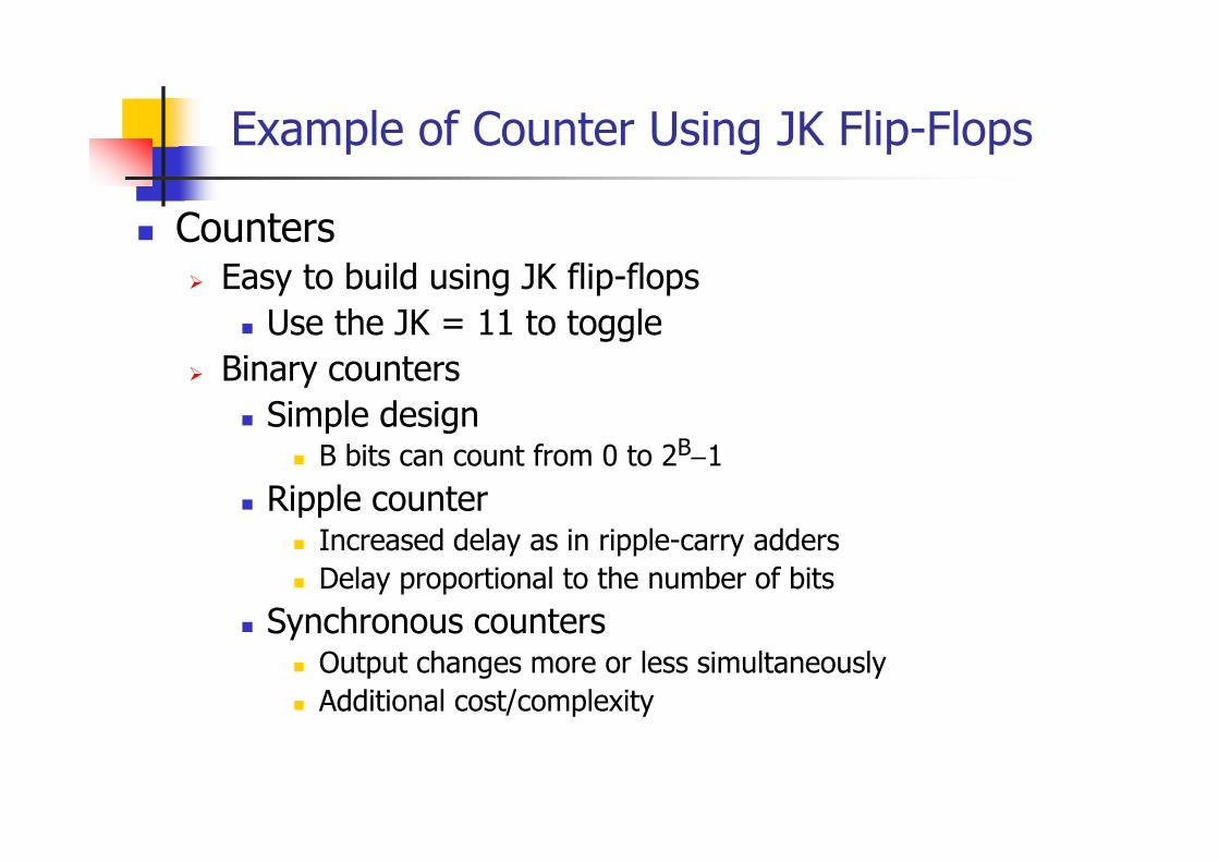
Example of Counter Using JK Flip-Flops
CountersEasy to build using JK flip-flops
Use the JK = 11 to toggleBinary counters
Simple designp gB bits can count from 0 to 2B−1
Ripple counterIncreased delay as in ripple-carry addersDelay proportional to the number of bits
Synchronous countersOutput changes more or less simultaneouslyAdditional cost/complexity
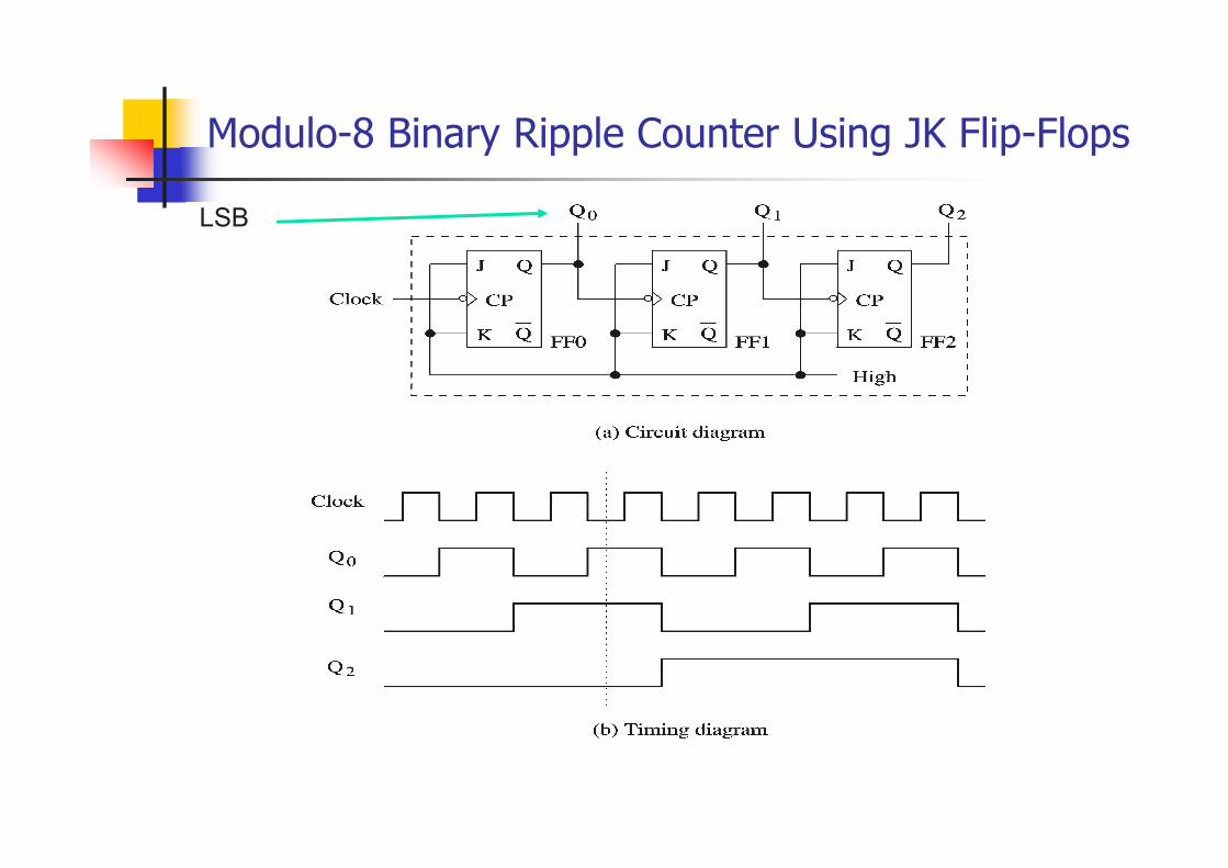
Modulo-8 Binary Ripple Counter Using JK Flip-Flops
LSB

Synchronous Modulo-8 Counter
Designed using the following simple ruleChange output if the preceding count bits are 1
Q1 changes whenever Q0 = 1Q2 changes whenever Q1Q0 = 11

Example Counters

Sequential Circuit Design
Sequential circuit consists of A combinational circuit that produces outputA feedback circuit
We use JK flip-flops for the feedback circuit
Si l t l i JK fli flSimple counter examples using JK flip-flopsProvides alternative counter designsWe know the output
Need to know the input combination that produces this outputUse an excitation table
Built from the truth table
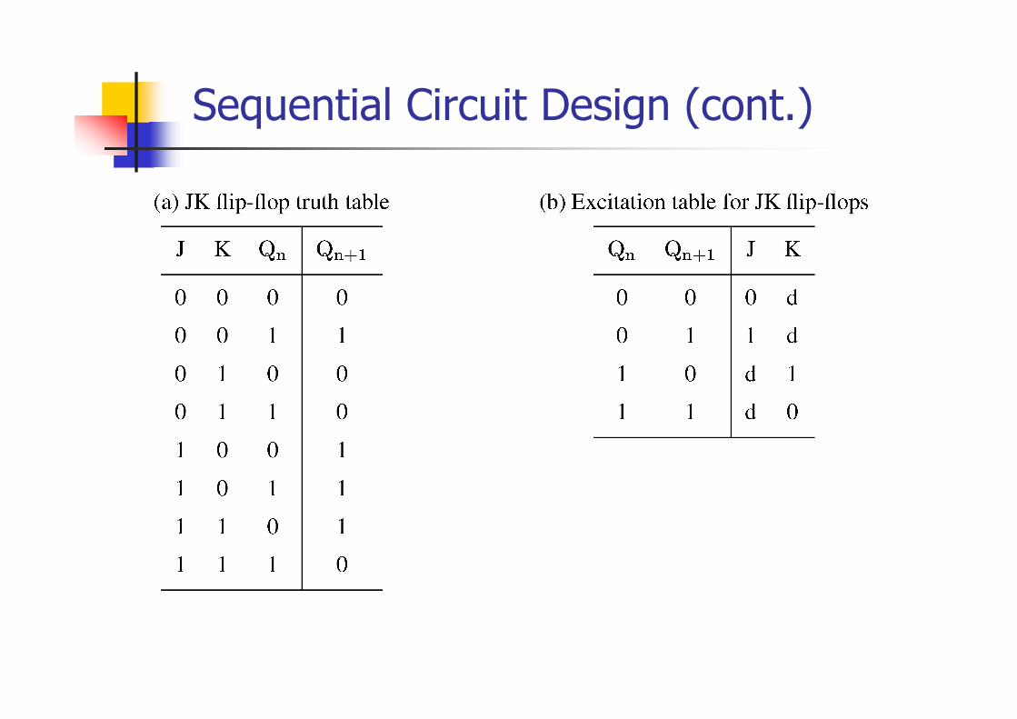
Sequential Circuit Design (cont.)

Sequential Circuit Design (cont.)
Build a design table that consists ofCurrent state outputNext state outputJK inputs for each flip-flop
Bi t lBinary counter example3-bit binary counter3 JK flip-flops are neededCurrent state and next state outputs are 3 bits each3 pairs of JK inputs
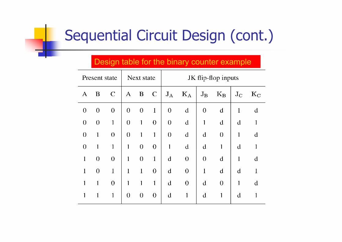
Sequential Circuit Design (cont.)
Design table for the binary counter example

Sequential Circuit Design (cont.)
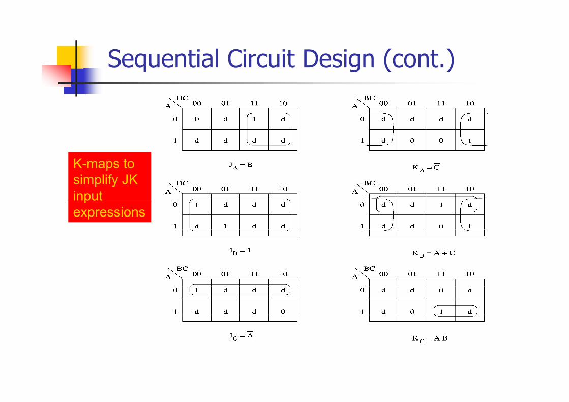
Use K-maps to simplify expressions for JK inputs
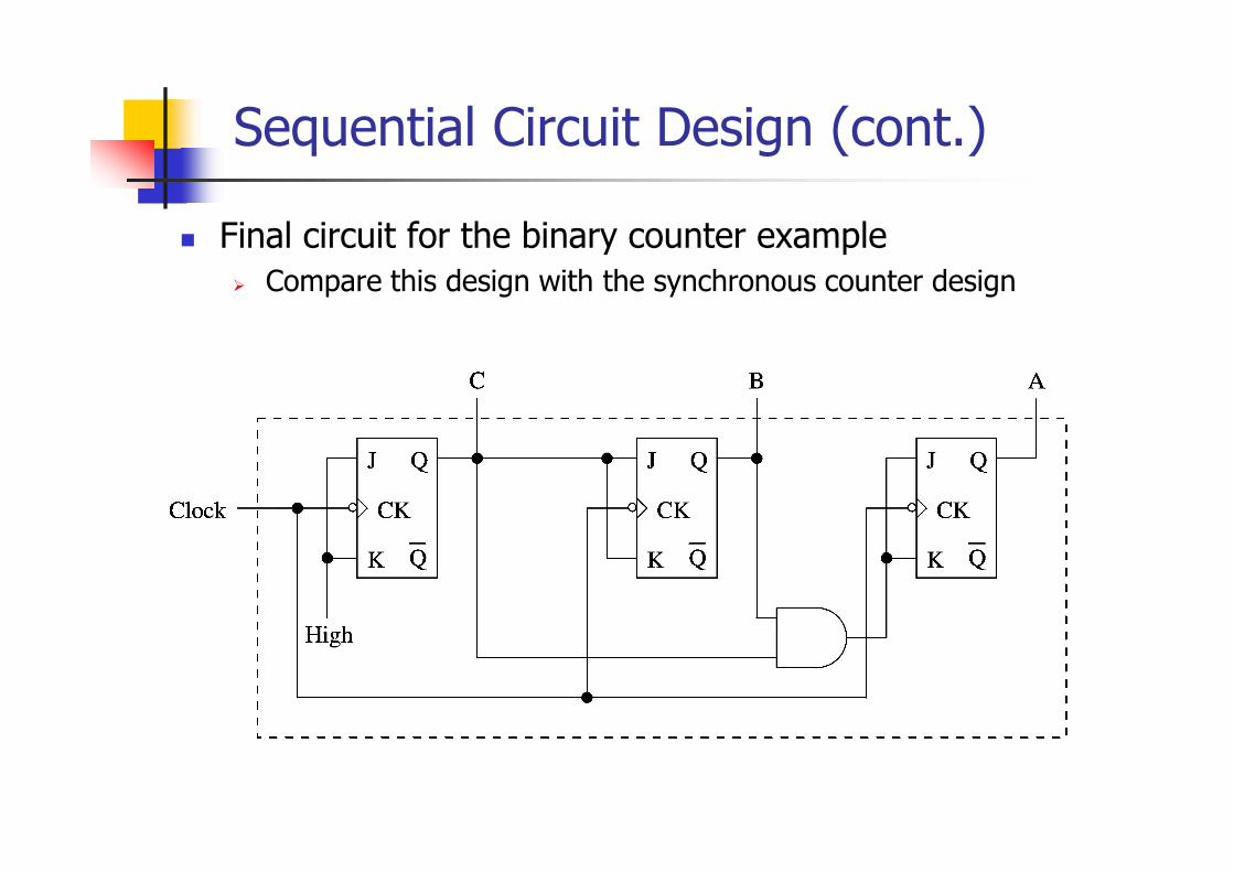
Sequential Circuit Design (cont.)
Final circuit for the binary counter exampleCompare this design with the synchronous counter design

Sequential Circuit Design (cont.)
A more general counter design
Does not step in sequence
0→3→5→7→6→0
Same design processOne significant change
Missing states1, 2, and 4Use don’t cares for these states

Sequential Circuit Design (cont.)
Design table for the general counter example
Sequential Circuit Design (cont.)
K-maps to simplify JK input pexpressions
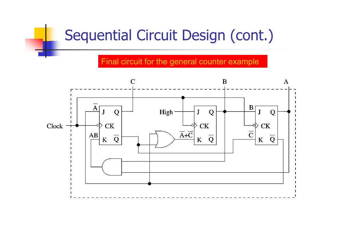
Sequential Circuit Design (cont.)
Final circuit for the general counter example

General Design Process
FSM can be used to express the behavior of a sequential circuit
Counters are a special caseState transitions are indicated by arrows with labels X/Y
X: inputs that cause system state changeX: inputs that cause system state changeY: output generated while moving to the next state
Look at two examplesEven-parity checkerPattern recognition

General Design Process (cont.)
Even-parity checkerFSM needs to remember one of two facts
Number of 1’s is odd or evenNeed only two states
0 input does not change the state1 input changes state1 input changes state
Simple example Complete the design as an exercise

General Design Process (cont.)
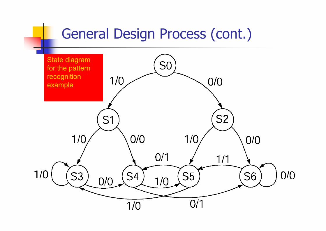
Pattern recognition exampleOutputs 1 whenever the input bit sequence has exactly two 0s in the last three input bitsFSM requires thee special states to during the initial phasephase
S0 − S2After that we need four states
S3: last two bits are 11S4: last two bits are 01S5: last two bits are 10S6: last two bits are 00
General Design Process (cont.)
State diagram for the pattern recognition example

General Design Process (cont.)
Steps in the design process1. Derive FSM2. State assignment
∗ Assign flip-flop states to the FSM statesNecessary to get an efficient design∗ Necessary to get an efficient design
3. Design table derivation∗ Derive a design table corresponding to the
assignment in the last step4. Logical expression derivation
∗ Use K-maps as in our previous examples5. Implementation
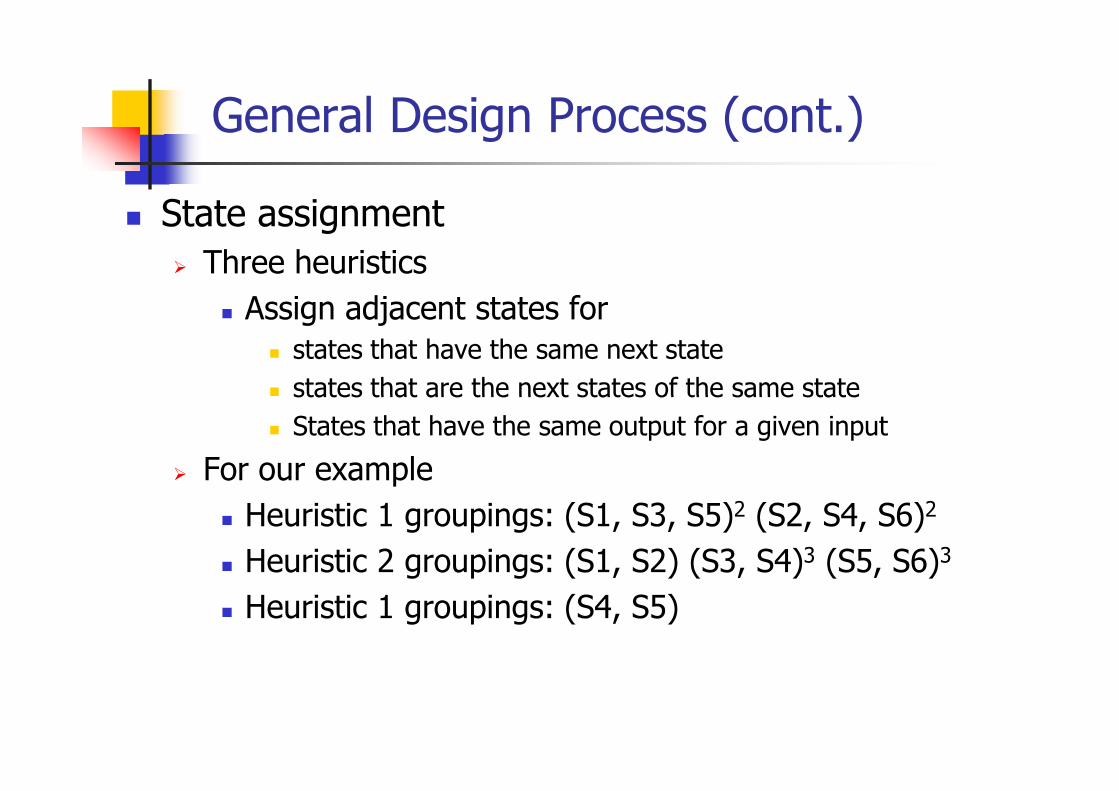
General Design Process (cont.)
State assignmentThree heuristics
Assign adjacent states forstates that have the same next statestates that are the next states of the same statestates that are the next states of the same stateStates that have the same output for a given input
For our exampleHeuristic 1 groupings: (S1, S3, S5)2 (S2, S4, S6)2
Heuristic 2 groupings: (S1, S2) (S3, S4)3 (S5, S6)3
Heuristic 1 groupings: (S4, S5)

General Design Process (cont.)
State table for the patternpattern recognition example

General Design Process (cont.)
State assignment
K-map for state assignment
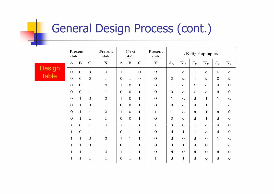
General Design Process (cont.)
Design table

General Design Process (cont.)
K-maps for JK inputs
K-map for the output
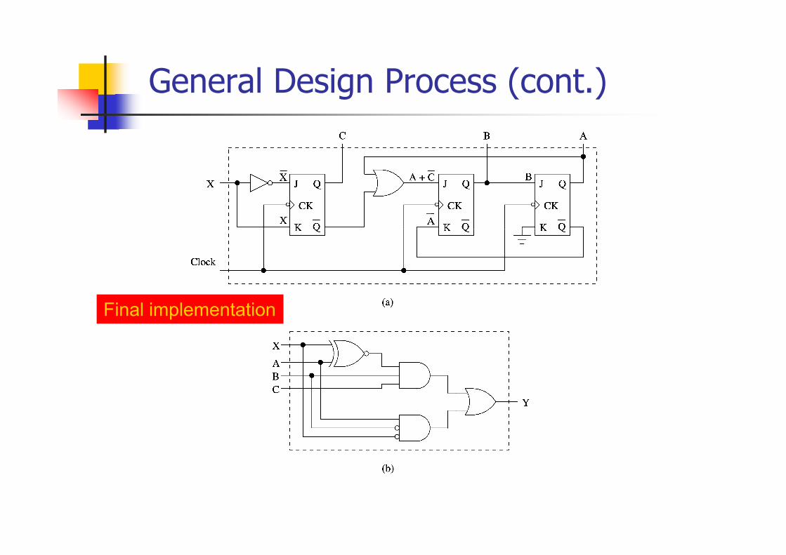
General Design Process (cont.)
Final implementation