
Digital Integrated Circuits Logic Families (Pt.I) · (i) Linear (ii) Digital Digital ICs classified...
16
Digital Integrated Circuits – Logic Families (Pt.I) Integrated circuits classified as (i) Linear (ii) Digital Digital ICs classified as per level of integration. These are like SSI, MSI, LSI, VLSI, ULSI and GSI as per the number of Gates. SSI (<12), MSI (12 to 99), LSI (100 to 9999), VLSI (10,000 to 99,999), ULSI (100,000 to 999,999) & GSI (1 Million or more) SSI - Basic gates & FFs MSI - More complex like adders, comparators LSI - Small digital systems like digital clocks calculator VLSI - Digital system on chip like large memory chips ULSI & GSI - Complex function – several boards of ICs
Transcript of Digital Integrated Circuits Logic Families (Pt.I) · (i) Linear (ii) Digital Digital ICs classified...
Digital Integrated Circuits – Logic Families (Pt.I)
Integrated circuits classified as
(i) Linear (ii) Digital
Digital ICs classified as per level of integration.
These are like SSI, MSI, LSI, VLSI, ULSI and GSI as per the number
of Gates.
SSI (<12), MSI (12 to 99), LSI (100 to 9999), VLSI (10,000 to
99,999), ULSI (100,000 to 999,999) & GSI (1 Million or more)
SSI - Basic gates & FFs
MSI - More complex like adders, comparators
LSI - Small digital systems like digital clocks calculator
VLSI - Digital system on chip like large memory chips
ULSI & GSI - Complex function – several boards of ICs
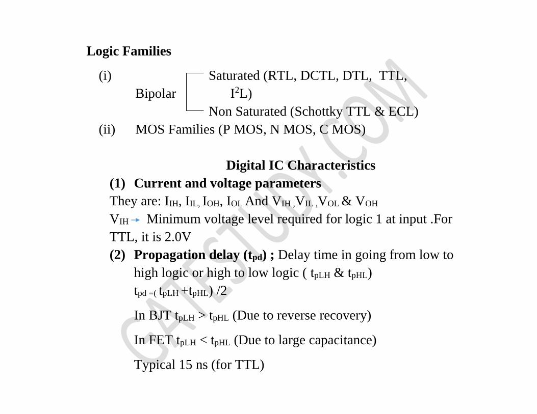
Logic Families
(i) Saturated (RTL, DCTL, DTL, TTL,
Bipolar I2L)
Non Saturated (Schottky TTL & ECL)
(ii) MOS Families (P MOS, N MOS, C MOS)
Digital IC Characteristics
(1) Current and voltage parameters
They are: IIH, IIL, IOH, IOL And VIH ,VIL ,VOL & VOH
VIH Minimum voltage level required for logic 1 at input .For
TTL, it is 2.0V
(2) Propagation delay (tpd) ; Delay time in going from low to
high logic or high to low logic ( tpLH & tpHL)
tpd =( tpLH +tpHL) /2
In BJT tpLH > tpHL (Due to reverse recovery)
In FET tpLH < tpHL (Due to large capacitance)
Typical 15 ns (for TTL)
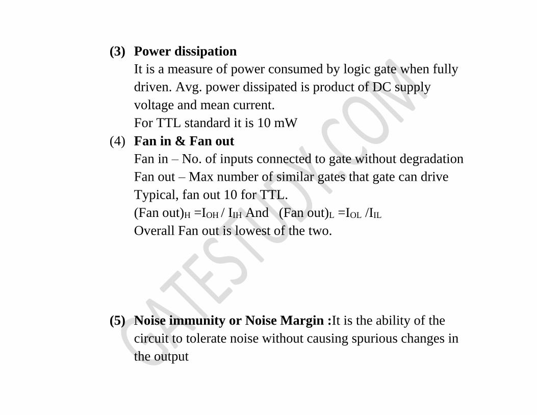
(3) Power dissipation
It is a measure of power consumed by logic gate when fully
driven. Avg. power dissipated is product of DC supply
voltage and mean current.
For TTL standard it is 10 mW
(4) Fan in & Fan out
Fan in – No. of inputs connected to gate without degradation
Fan out – Max number of similar gates that gate can drive
Typical, fan out 10 for TTL.
(Fan out)H =IOH / IIH And (Fan out)L =IOL /IIL
Overall Fan out is lowest of the two.
(5) Noise immunity or Noise Margin :It is the ability of the
circuit to tolerate noise without causing spurious changes in
the output
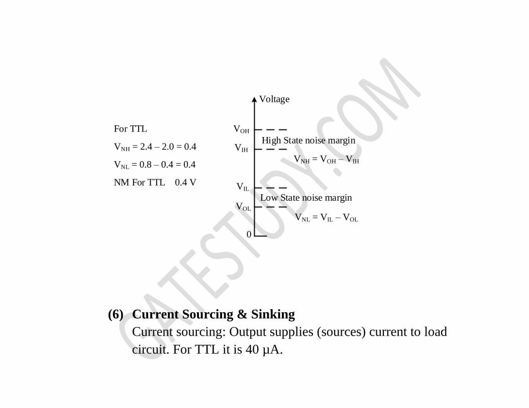
High State noise margin
VNH = VOH – VIH
Low State noise margin
VNL = VIL – VOL
VOH
VIH
VIL
VOL
Voltage
0
For TTL
VNH = 2.4 – 2.0 = 0.4
VNL = 0.8 – 0.4 = 0.4
NM For TTL 0.4 V
(6) Current Sourcing & Sinking
Current sourcing: Output supplies (sources) current to load
circuit. For TTL it is 40 µA.
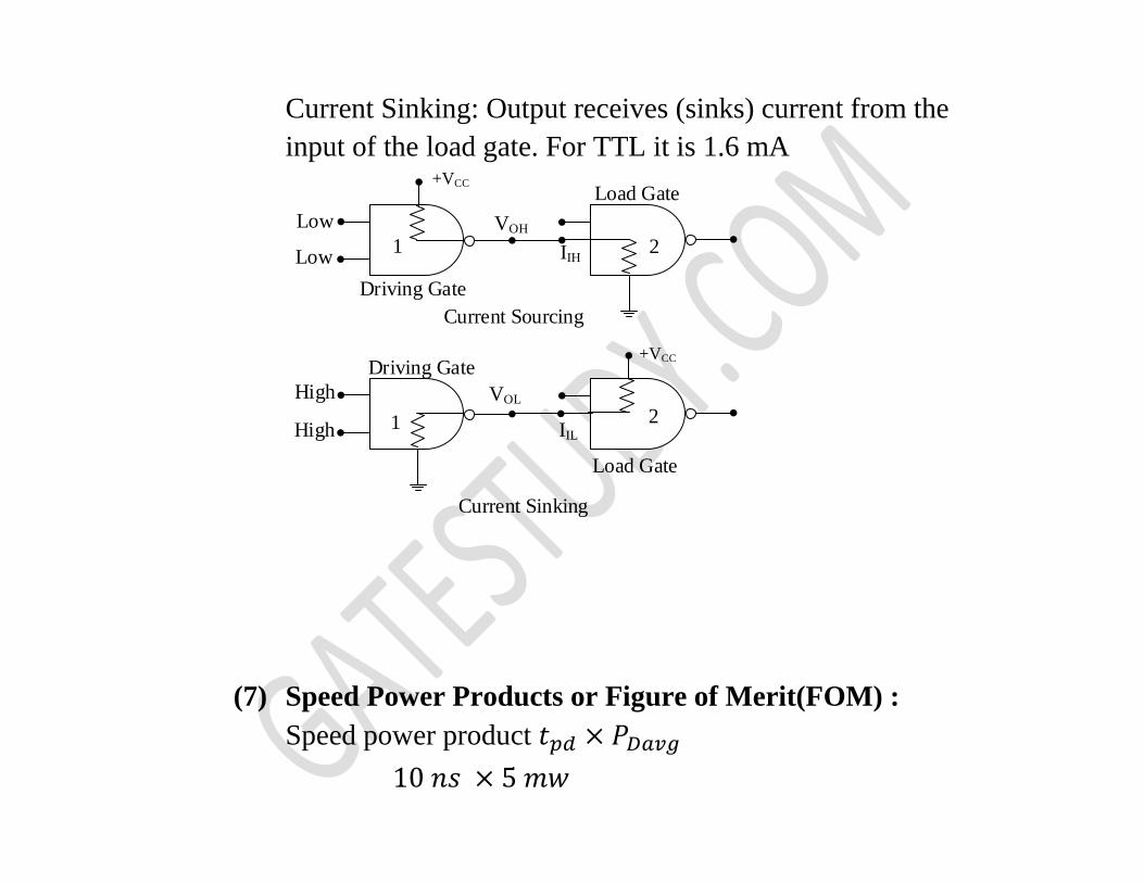
Current Sinking: Output receives (sinks) current from the
input of the load gate. For TTL it is 1.6 mA
Low
Low
High
High
Current Sourcing
Current Sinking
1 2
1 2
+VCC
+VCC
VOL
IIL
IIH
Driving Gate
Driving Gate
Load Gate
Load Gate
VOH
(7) Speed Power Products or Figure of Merit(FOM) :
Speed power product 𝑡𝑝𝑑 × 𝑃𝐷𝑎𝑣𝑔
10 𝑛𝑠 × 5 𝑚𝑤
50 𝑝𝑖𝑐𝑜 − 𝐽𝑜𝑢𝑙𝑒𝑠 (𝑃𝐽)
When delay in ns & Pavg in mw, speed power
Product in pico – Joules
Low value desirable.
For TTL (Std.) – 100 pico - Joules
Bipolar Logic Families
Bipolar ICs use resistors, BJT, and diodes. They are either
saturated logic or non- saturated.
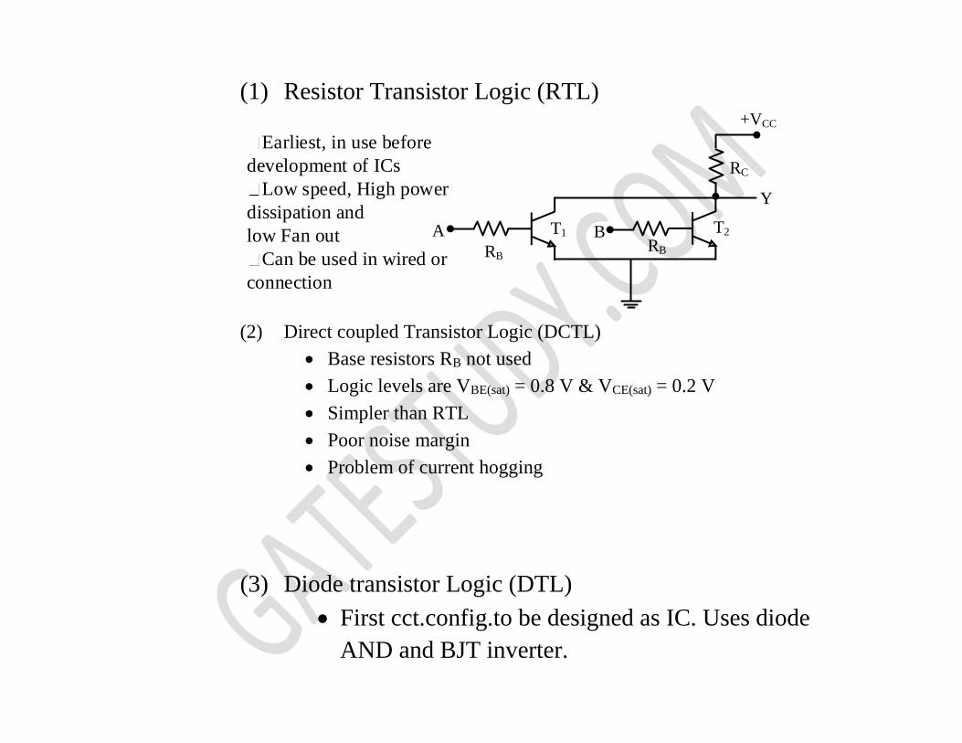
(1) Resistor Transistor Logic (RTL)
A
Y
+VCC
RC
BRB
T2T1
RB
Earliest, in use before
development of ICs
Low speed, High power
dissipation and
low Fan out
Can be used in wired or
connection
(2) Direct coupled Transistor Logic (DCTL)
Base resistors RB not used
Logic levels are VBE(sat) = 0.8 V & VCE(sat) = 0.2 V
Simpler than RTL
Poor noise margin
Problem of current hogging
(3) Diode transistor Logic (DTL)
First cct.config.to be designed as IC. Uses diode
AND and BJT inverter.
It has limitation of no low and constant output
impedance in both the states.
(4) Transistor Transistor Logic (TTL)
Problem of DTL eliminated by totem pole output.
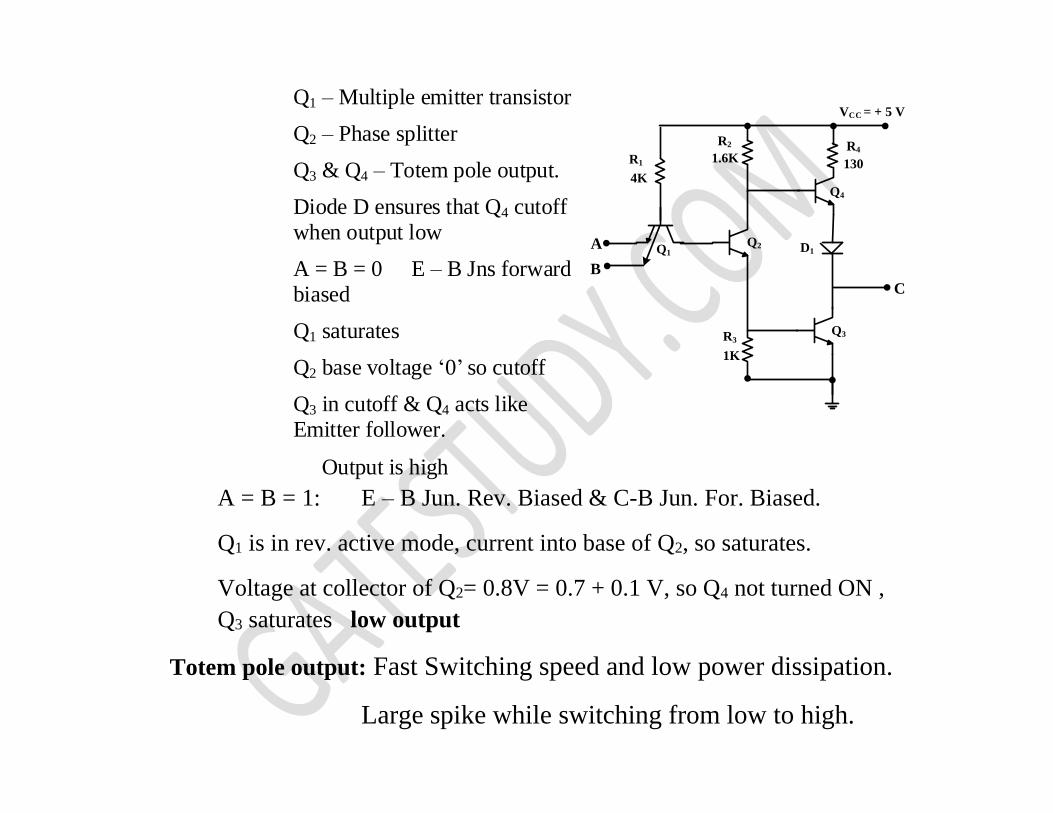
Q1Q2
Q4
Q3
C
A
1K
4K
1.6K 130
VCC = + 5 V
R4R2
R1
R3
B
D1
Q1 – Multiple emitter transistor
Q2 – Phase splitter
Q3 & Q4 – Totem pole output.
Diode D ensures that Q4 cutoff when output low
A = B = 0 E – B Jns forward
biased
Q1 saturates
Q2 base voltage 0 so cutoff
Q3 in cutoff & Q4 acts like Emitter follower.
Output is high
A = B = 1: E – B Jun. Rev. Biased & C-B Jun. For. Biased.
Q1 is in rev. active mode, current into base of Q2, so saturates.
Voltage at collector of Q2= 0.8V = 0.7 + 0.1 V, so Q4 not turned ON ,
Q3 saturates low output
Totem pole output: Fast Switching speed and low power dissipation.
Large spike while switching from low to high.
Open collector output: Wired AND & OR operation.
Tristate output: Incorporates benefit of totem pole and open
collector.
TTL sub families are in common use.
Schottky TTL:
The main purpose is to increase speed.
Four sub families that use Schottky diodes and transistors (74S,
74LS, 74ALS and 74AS).
Schottky transistor use Schottky clamp diode across collector
base junction of BJT to prevent its saturation.
Schottky carrier diodes are also called hot carrier diodes.
TTL sub families speed- power comparison
Minimizing Power Minimizing delay time
Family
Propagatio
n
Delay
(ns)
Power
Dissipatio
n
(mW)
Speed/P
ower
Product
(pJ)
Family
Propagat
ion
Delay
(ns)
Power
Dissipati
on
(mW)
SPD/P
WR
Produ
ct
(pJ)
TTL 10 10 100 TTL 10 10 100
L TTL 33 1 33 H TTL 6 22 132
LS
TTL
9 2 18 S TTL 3 19 67
ALS 4 1.2 4.8 AS 1.7 8 13.6
Two approaches (i)Minimizing power (ii)minimizing delay time
LTTL, LSTTL, ALS all have letter L for low power. ALS series
has the best characteristics.
HTTL, STTL, AS are high speed.AS is the best.
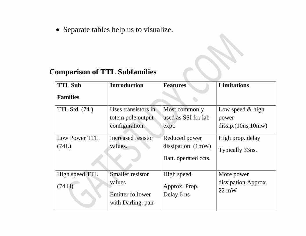
Separate tables help us to visualize.
Comparison of TTL Subfamilies
TTL Sub
Families
Introduction Features Limitations
TTL Std. (74 ) Uses transistors in
totem pole output
configuration.
Most commonly
used as SSI for lab
expt.
Low speed & high
power
dissip.(10ns,10mw)
Low Power TTL
(74L)
Increased resistor
values.
Reduced power
dissipation (1mW)
Batt. operated ccts.
High prop. delay
Typically 33ns.
High speed TTL
(74 H)
Smaller resistor
values
Emitter follower
with Darling. pair
High speed
Approx. Prop.
Delay 6 ns
More power
dissipation Approx.
22 mW
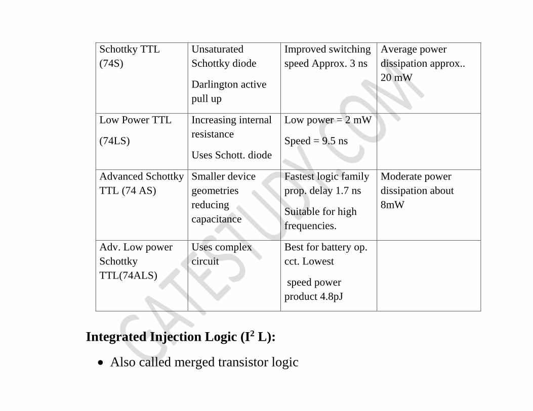
Schottky TTL
(74S)
Unsaturated
Schottky diode
Darlington active
pull up
Improved switching
speed Approx. 3 ns
Average power
dissipation approx..
20 mW
Low Power TTL
(74LS)
Increasing internal
resistance
Uses Schott. diode
Low power = 2 mW
Speed = 9.5 ns
Advanced Schottky
TTL (74 AS)
Smaller device
geometries
reducing
capacitance
Fastest logic family
prop. delay 1.7 ns
Suitable for high
frequencies.
Moderate power
dissipation about
8mW
Adv. Low power
Schottky
TTL(74ALS)
Uses complex
circuit
Best for battery op.
cct. Lowest
speed power
product 4.8pJ
Integrated Injection Logic (I2 L):
Also called merged transistor logic
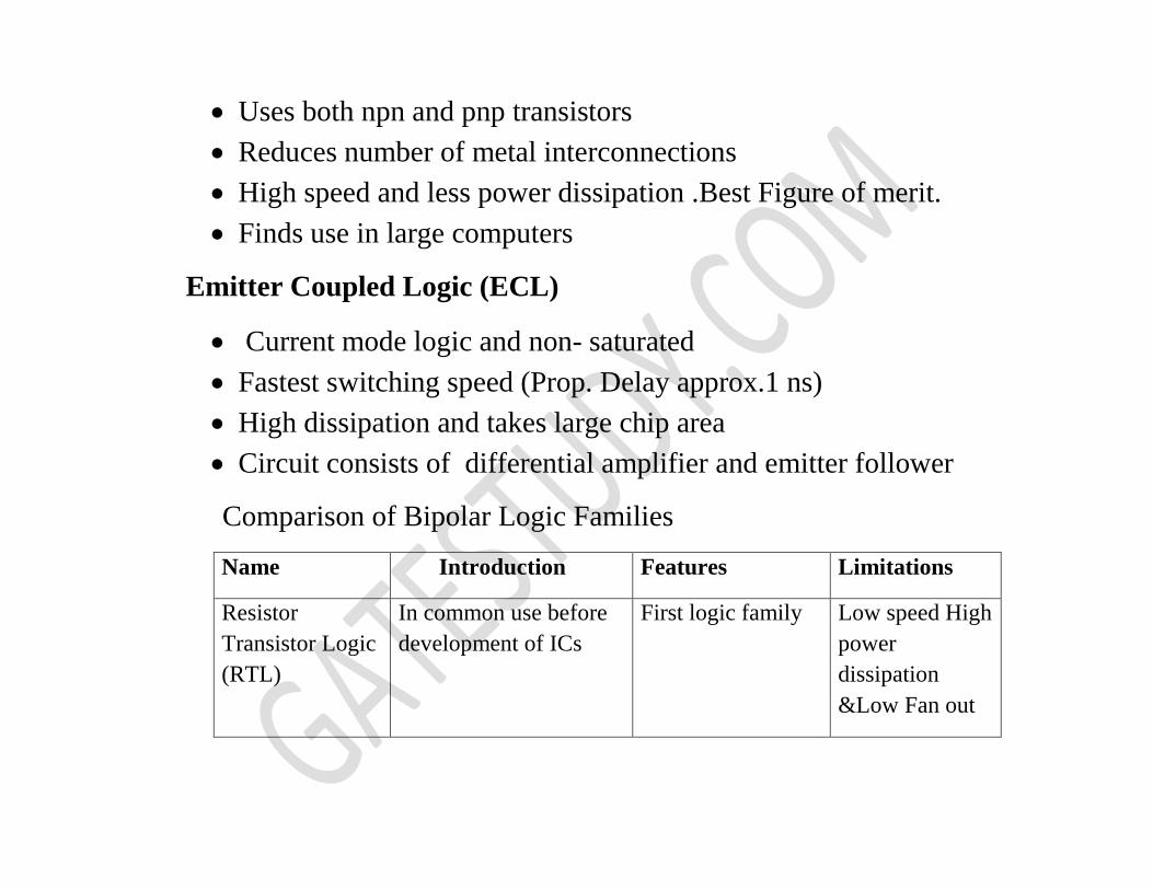
Uses both npn and pnp transistors
Reduces number of metal interconnections
High speed and less power dissipation .Best Figure of merit.
Finds use in large computers
Emitter Coupled Logic (ECL)
Current mode logic and non- saturated
Fastest switching speed (Prop. Delay approx.1 ns)
High dissipation and takes large chip area
Circuit consists of differential amplifier and emitter follower
Comparison of Bipolar Logic Families
Name Introduction Features Limitations
Resistor
Transistor Logic
(RTL)
In common use before
development of ICs
First logic family Low speed High
power
dissipation
&Low Fan out
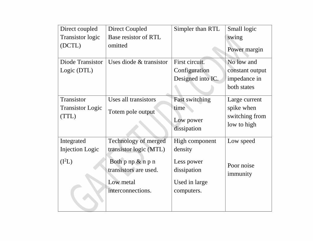
Direct coupled
Transistor logic
(DCTL)
Direct Coupled
Base resistor of RTL
omitted
Simpler than RTL Small logic
swing
Power margin
Diode Transistor
Logic (DTL)
Uses diode & transistor First circuit.
Configuration
Designed into IC.
No low and
constant output
impedance in
both states
Transistor
Transistor Logic
(TTL)
Uses all transistors
Totem pole output
Fast switching
time
Low power
dissipation
Large current
spike when
switching from
low to high
Integrated
Injection Logic
(I2L)
Technology of merged
transistor logic (MTL)
Both p np & n p n
transistors are used.
Low metal
interconnections.
High component
density
Less power
dissipation
Used in large
computers.
Low speed
Poor noise
immunity
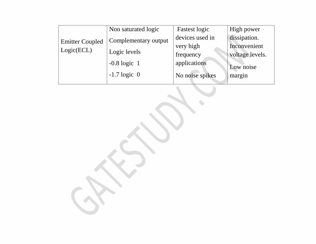
Emitter Coupled
Logic(ECL)
Non saturated logic
Complementary output
Logic levels
-0.8 logic 1
-1.7 logic 0
Fastest logic
devices used in
very high
frequency
applications
No noise spikes
High power
dissipation.
Inconvenient
voltage levels.
Low noise
margin


![[C. Y. Chang, Simon M. Sze] ULSI Devices(BookFi.org)](https://static.fdocuments.us/doc/165x107/55cf9409550346f57b9f371b/c-y-chang-simon-m-sze-ulsi-devicesbookfiorg.jpg)


