
Digital Integrated Circuits Lecture 10:...
32
DIC-Lec10 [email protected] 1 Digital Integrated Circuits Lecture 10: Wires Chih-Wei Liu VLSI Signal Processing LAB National Chiao Tung University [email protected]
Transcript of Digital Integrated Circuits Lecture 10:...
DIC-Lec10 [email protected] 1
Digital Integrated CircuitsLecture 10: Wires
Chih-Wei Liu
VLSI Signal Processing LAB
National Chiao Tung University
DIC-Lec10 [email protected] 2
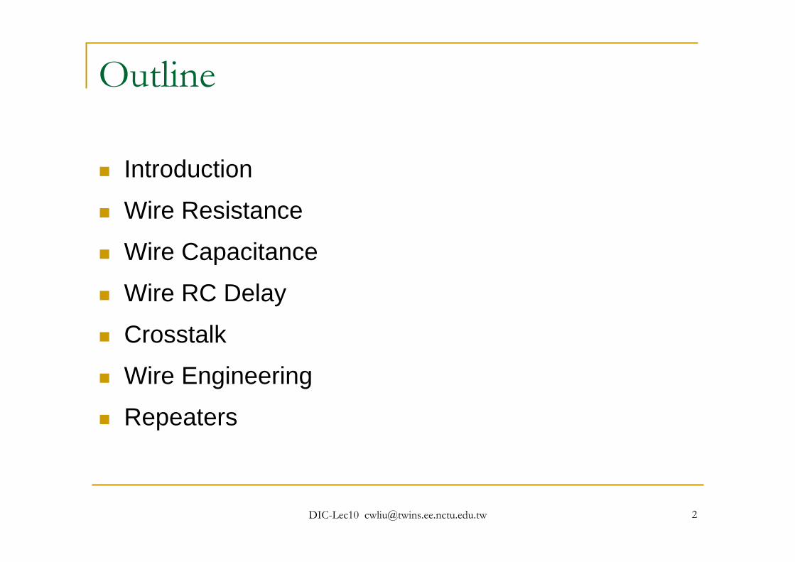
Outline
Introduction
Wire Resistance
Wire Capacitance
Wire RC Delay
Crosstalk
Wire Engineering
Repeaters
DIC-Lec10 [email protected] 3
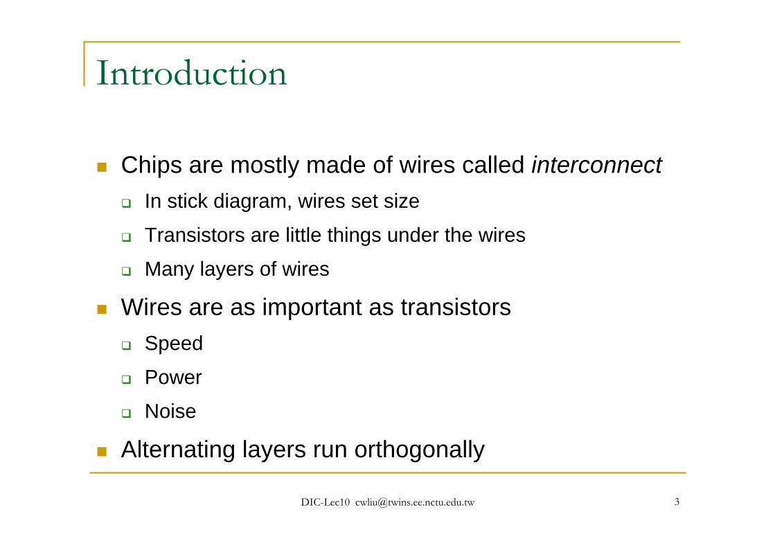
Introduction
Chips are mostly made of wires called interconnectIn stick diagram, wires set size
Transistors are little things under the wires
Many layers of wires
Wires are as important as transistorsSpeed
Power
Noise
Alternating layers run orthogonally
DIC-Lec10 [email protected] 4
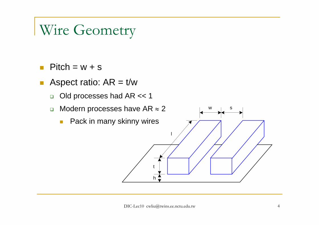
Wire Geometry
Pitch = w + s
Aspect ratio: AR = t/wOld processes had AR << 1
Modern processes have AR ≈ 2Pack in many skinny wires
l
w s
t
h
DIC-Lec10 [email protected] 5
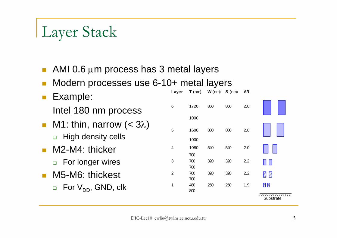
Layer Stack
AMI 0.6 μm process has 3 metal layersModern processes use 6-10+ metal layersExample:Intel 180 nm processM1: thin, narrow (< 3λ)
High density cells
M2-M4: thickerFor longer wires
M5-M6: thickestFor VDD, GND, clk
Layer T (nm) W (nm) S (nm) AR
6 1720 860 860 2.0
1000
5 1600 800 800 2.0
1000
4 1080 540 540 2.0
7003 700 320 320 2.2
7002 700 320 320 2.2
7001 480 250 250 1.9
800
Substrate
DIC-Lec10 [email protected] 7
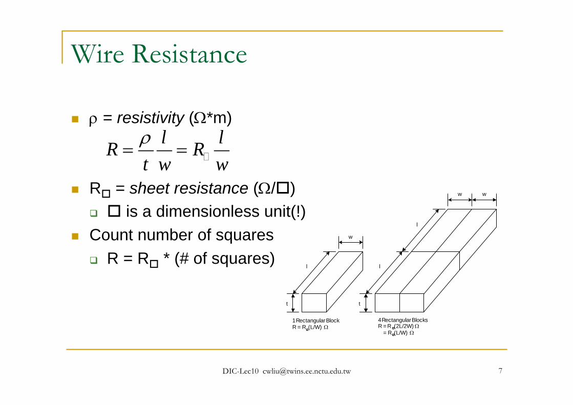
Wire Resistance
ρ = resistivity (Ω*m)
R = sheet resistance (Ω/ )is a dimensionless unit(!)
Count number of squaresR = R * (# of squares)
l
w
t
1 Rectangular BlockR = R (L/W) Ω
4 Rectangular BlocksR = R (2L/2W) Ω = R (L/W) Ω
t
l
w w
l
l lR Rt w wρ
= =
DIC-Lec10 [email protected] 8
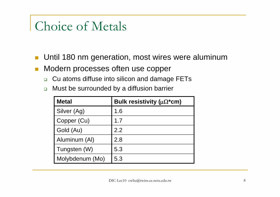
Choice of Metals
Until 180 nm generation, most wires were aluminumModern processes often use copper
Cu atoms diffuse into silicon and damage FETsMust be surrounded by a diffusion barrier
5.3Molybdenum (Mo)5.3Tungsten (W)2.8Aluminum (Al)2.2Gold (Au)1.7Copper (Cu)1.6Silver (Ag)Bulk resistivity (μΩ*cm)Metal
DIC-Lec10 [email protected] 9
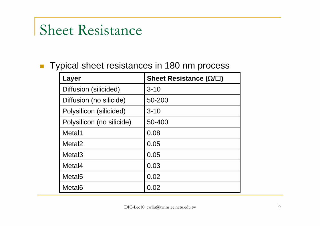
Sheet Resistance
Typical sheet resistances in 180 nm process
0.08Metal10.05Metal20.05Metal30.03Metal4
0.02Metal60.02Metal5
50-400Polysilicon (no silicide)3-10Polysilicon (silicided)50-200Diffusion (no silicide)3-10Diffusion (silicided)Sheet Resistance (Ω/ )Layer
DIC-Lec10 [email protected] 10
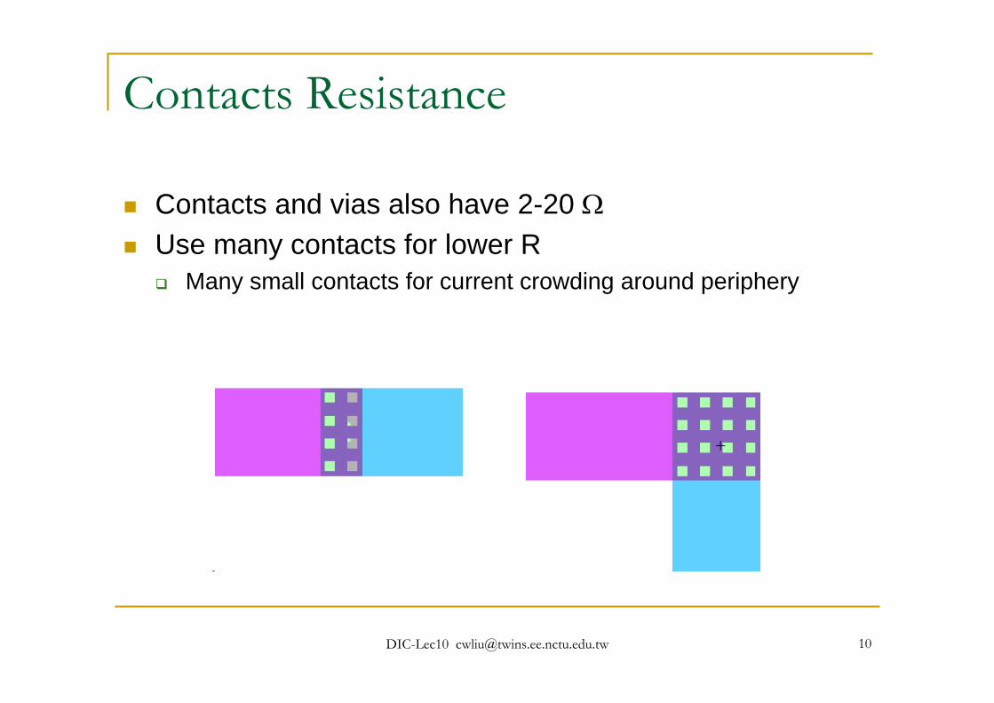
Contacts Resistance
Contacts and vias also have 2-20 ΩUse many contacts for lower R
Many small contacts for current crowding around periphery
DIC-Lec10 [email protected] 11
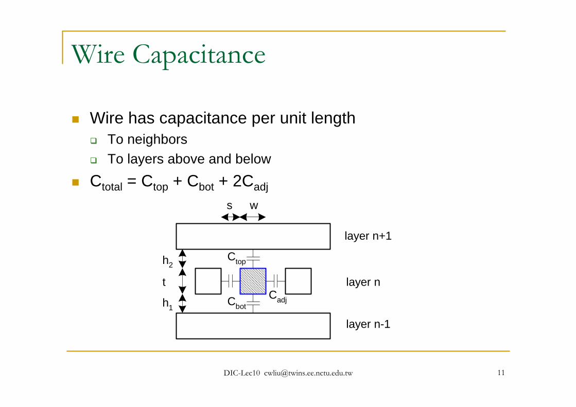
Wire Capacitance
Wire has capacitance per unit lengthTo neighborsTo layers above and below
Ctotal = Ctop + Cbot + 2Cadj
layer n+1
layer n
layer n-1
Cadj
Ctop
Cbot
ws
t
h1
h2
DIC-Lec10 [email protected] 12
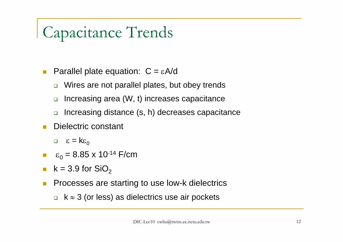
Capacitance Trends
Parallel plate equation: C = εA/dWires are not parallel plates, but obey trends
Increasing area (W, t) increases capacitance
Increasing distance (s, h) decreases capacitance
Dielectric constantε = kε0
ε0 = 8.85 x 10⁻¹⁴ F/cmk = 3.9 for SiO2
Processes are starting to use low-k dielectricsk ≈ 3 (or less) as dielectrics use air pockets

DIC-Lec10 [email protected] 13
M2 Capacitance Data
Typical wires have ~ 0.2 fF/μmCompare to 2 fF/μm for gate capacitance
0
50
100
150
200
250
300
350
400
0 500 1000 1500 2000
Cto
tal (
aF/μ
m)
w (nm)
Isolated
M1, M3 planes
s = 320s = 480s = 640s= 8
s = 320s = 480s = 640
s= 8
DIC-Lec10 [email protected] 14
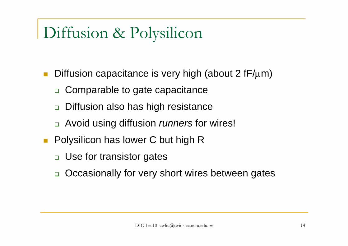
Diffusion & Polysilicon
Diffusion capacitance is very high (about 2 fF/μm)Comparable to gate capacitance
Diffusion also has high resistance
Avoid using diffusion runners for wires!
Polysilicon has lower C but high R
Use for transistor gates
Occasionally for very short wires between gates
DIC-Lec10 [email protected] 15
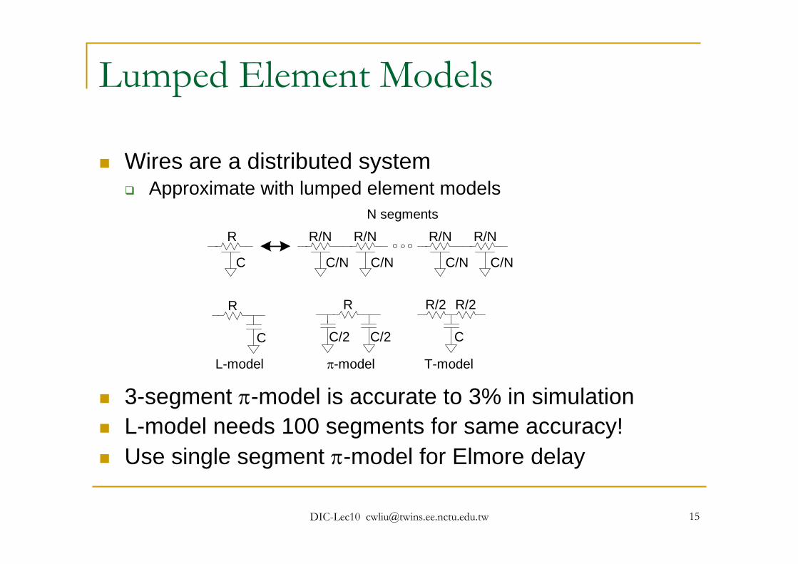
Lumped Element Models
Wires are a distributed systemApproximate with lumped element models
3-segment π-model is accurate to 3% in simulationL-model needs 100 segments for same accuracy!Use single segment π-model for Elmore delay
C
R
C/N
R/N
C/N
R/N
C/N
R/N
C/N
R/N
R
C
L-model
R
C/2 C/2
R/2 R/2
C
N segments
π-model T-model
DIC-Lec10 [email protected] 16
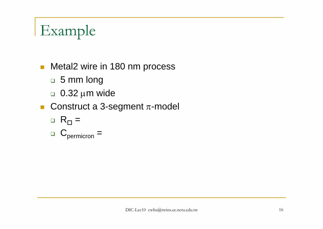
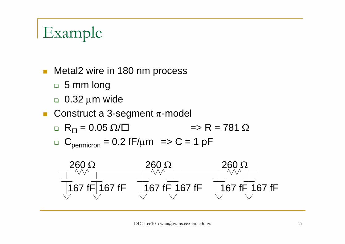
Example
Metal2 wire in 180 nm process5 mm long0.32 μm wide
Construct a 3-segment π-modelR =Cpermicron =
DIC-Lec10 [email protected] 17
Example
Metal2 wire in 180 nm process5 mm long0.32 μm wide
Construct a 3-segment π-modelR = 0.05 Ω/ => R = 781 ΩCpermicron = 0.2 fF/μm => C = 1 pF
260 Ω
167 fF 167 fF
260 Ω
167 fF 167 fF
260 Ω
167 fF 167 fF
DIC-Lec10 [email protected] 18
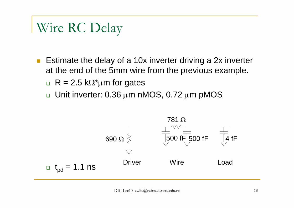
Wire RC Delay
Estimate the delay of a 10x inverter driving a 2x inverter at the end of the 5mm wire from the previous example.
R = 2.5 kΩ*μm for gatesUnit inverter: 0.36 μm nMOS, 0.72 μm pMOS
tpd = 1.1 ns
781 Ω
500 fF 500 fF
Driver Wire
4 fF
Load
690 Ω
DIC-Lec10 [email protected] 19
Crosstalk
A capacitor does not like to change its voltage instantaneously.
A wire has high capacitance to its neighbor.When the neighbor switches from 1-> 0 or 0->1, the wire tends to switch too.
Called capacitive coupling or crosstalk.
Crosstalk effectsNoise on nonswitching wires
Increased delay on switching wires
DIC-Lec10 [email protected] 20
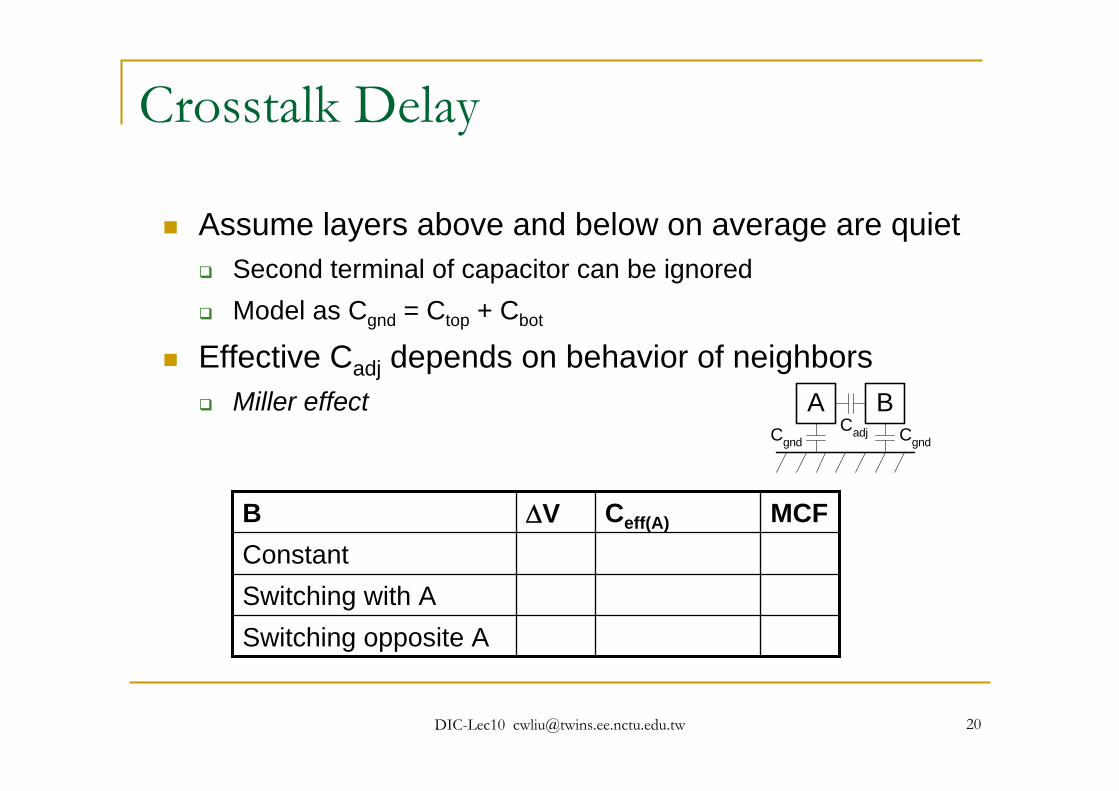
Crosstalk Delay
Assume layers above and below on average are quietSecond terminal of capacitor can be ignoredModel as Cgnd = Ctop + Cbot
Effective Cadj depends on behavior of neighborsMiller effect A B
CadjCgnd Cgnd
Switching opposite ASwitching with AConstant
MCFCeff(A)ΔVB
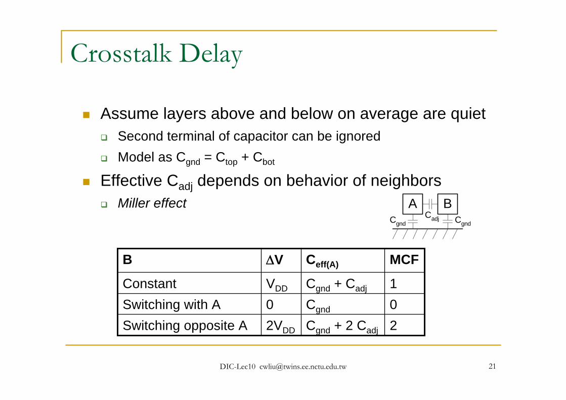
DIC-Lec10 [email protected] 21
Crosstalk Delay
Assume layers above and below on average are quietSecond terminal of capacitor can be ignoredModel as Cgnd = Ctop + Cbot
Effective Cadj depends on behavior of neighborsMiller effect A B
CadjCgnd Cgnd
2Cgnd + 2 Cadj2VDDSwitching opposite A0Cgnd0Switching with A1Cgnd + CadjVDDConstant
MCFCeff(A)ΔVB
DIC-Lec10 [email protected] 22
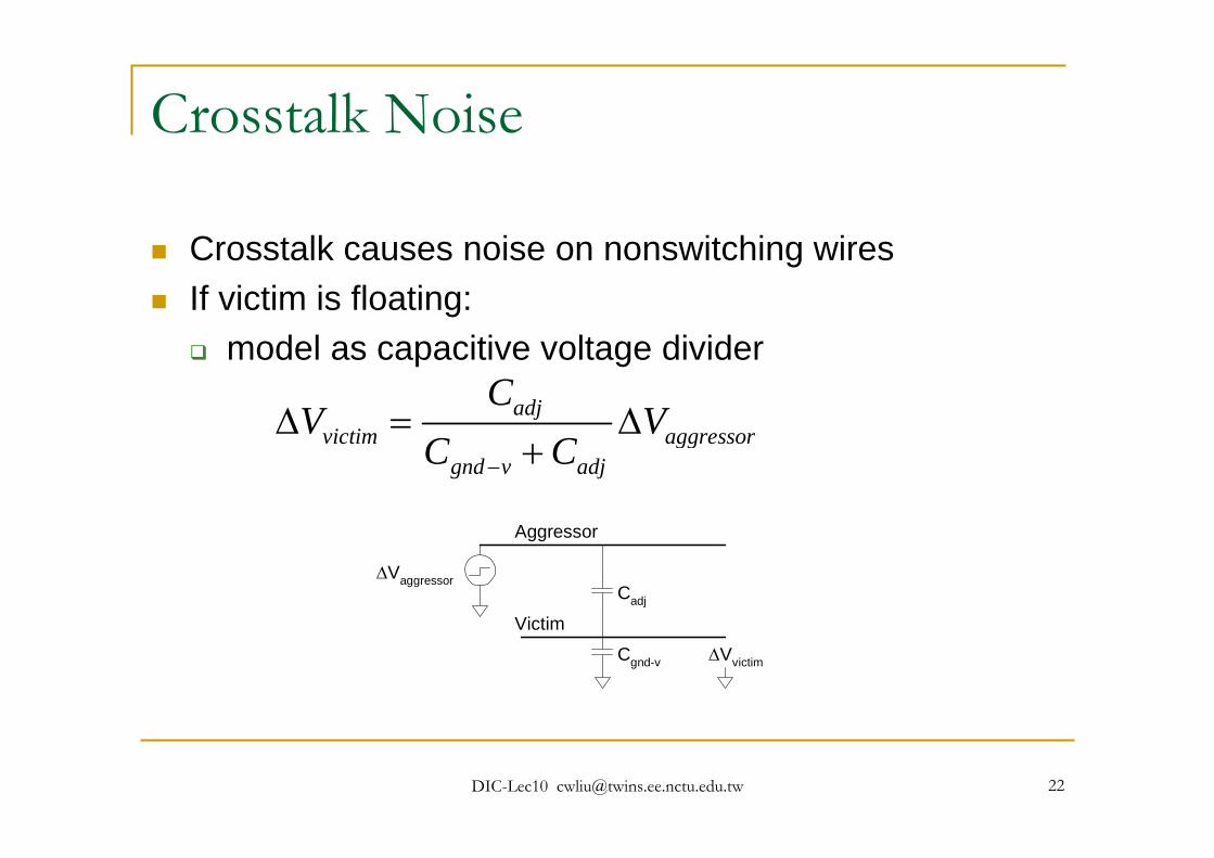
Crosstalk Noise
Crosstalk causes noise on nonswitching wiresIf victim is floating:
model as capacitive voltage divider
Cadj
Cgnd-v
Aggressor
Victim
ΔVaggressor
ΔVvictim
adjvictim aggressor
gnd v adj
CV V
C C−
Δ = Δ+
DIC-Lec10 [email protected] 23
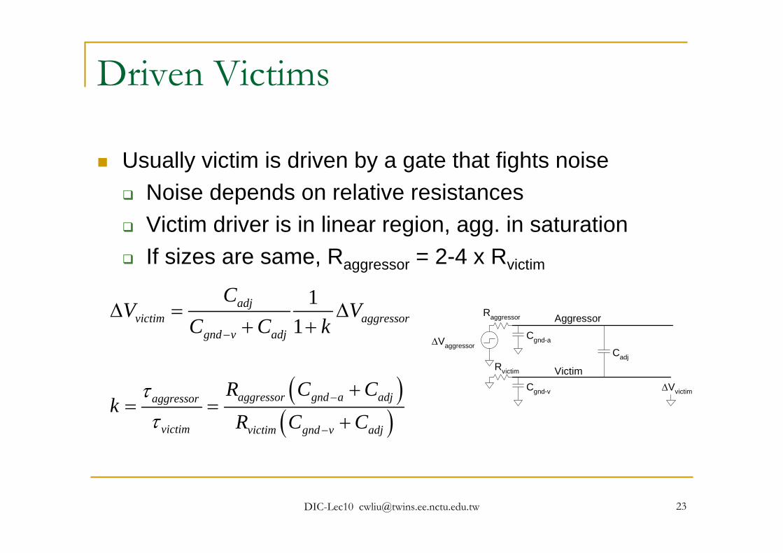
Driven Victims
Usually victim is driven by a gate that fights noiseNoise depends on relative resistancesVictim driver is in linear region, agg. in saturationIf sizes are same, Raggressor = 2-4 x Rvictim
11
adjvictim aggressor
gnd v adj
CV V
C C k−
Δ = Δ+ +
( )( )
aggressor gnd a adjaggressor
victim victim gnd v adj
R C Ck
R C Cττ
−
−
+= =
+
Cadj
Cgnd-v
Aggressor
Victim
ΔVaggressor
ΔVvictim
Raggressor
Rvictim
Cgnd-a
DIC-Lec10 [email protected] 24
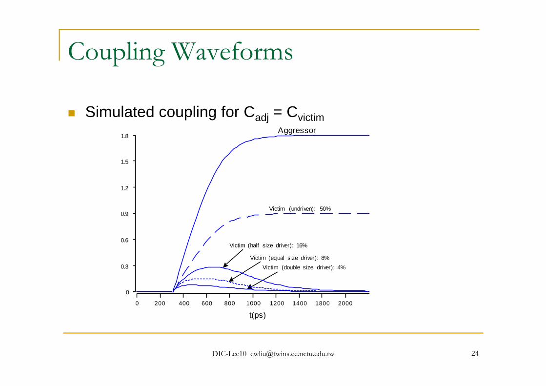
Coupling Waveforms
Aggressor
Victim (undriven): 50%
Victim (half size driver): 16%
Victim (equal size driver): 8%Victim (double size driver): 4%
t (ps)0 200 400 600 800 1000 1200 1400 1800 2000
0
0.3
0.6
0.9
1.2
1.5
1.8
Simulated coupling for Cadj = Cvictim

DIC-Lec10 [email protected] 25
Noise Implications
So what if we have noise?If the noise is less than the noise margin, nothing happensStatic CMOS logic will eventually settle to correct output even if disturbed by large noise spikes
But glitches cause extra delayAlso cause extra power from false transitions
Dynamic logic never recovers from glitchesMemories and other sensitive circuits also can produce the wrong answer
DIC-Lec10 [email protected] 26
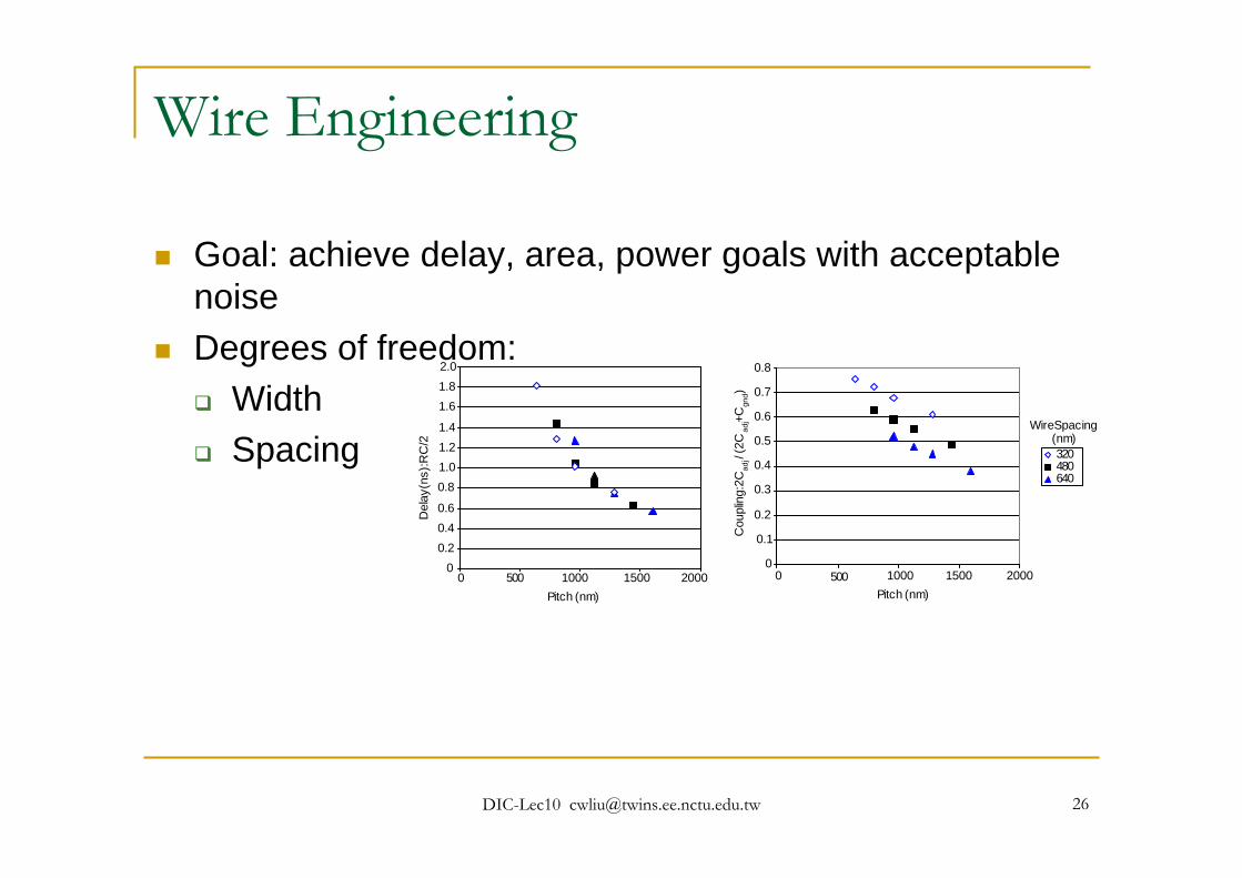
Wire Engineering
Goal: achieve delay, area, power goals with acceptable noiseDegrees of freedom:
Width Spacing
Del
ay (n
s): R
C/2
Wire Spacing(nm)
Cou
plin
g: 2C
adj /
(2C
adj+C
gnd)
00.20.40.6
0.81.01.21.4
1.61.82.0
0 500 1000 1500 20000
0.1
0.2
0.3
0.4
0.5
0.6
0.7
0.8
0 500 1000 1500 2000
320480640
Pitch (nm)Pitch (nm)
DIC-Lec10 [email protected] 27
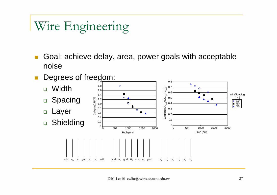
Wire Engineering
Goal: achieve delay, area, power goals with acceptable noiseDegrees of freedom:
Width SpacingLayerShielding
Del
ay (n
s): R
C/2
Wire Spacing(nm)
Cou
plin
g: 2C
adj /
(2C
adj+C
gnd)
00.20.40.6
0.81.01.21.4
1.61.82.0
0 500 1000 1500 20000
0.1
0.2
0.3
0.4
0.5
0.6
0.7
0.8
0 500 1000 1500 2000
320480640
Pitch (nm)Pitch (nm)
vdd a0a1gnd a2vdd b0 a1 a2 b2vdd a0 a1 gnd a2 a3 vdd gnd a0 b1
DIC-Lec10 [email protected] 28
Repeaters
R and C are proportional to lRC delay is proportional to l2
Unacceptably great for long wires
DIC-Lec10 [email protected] 29
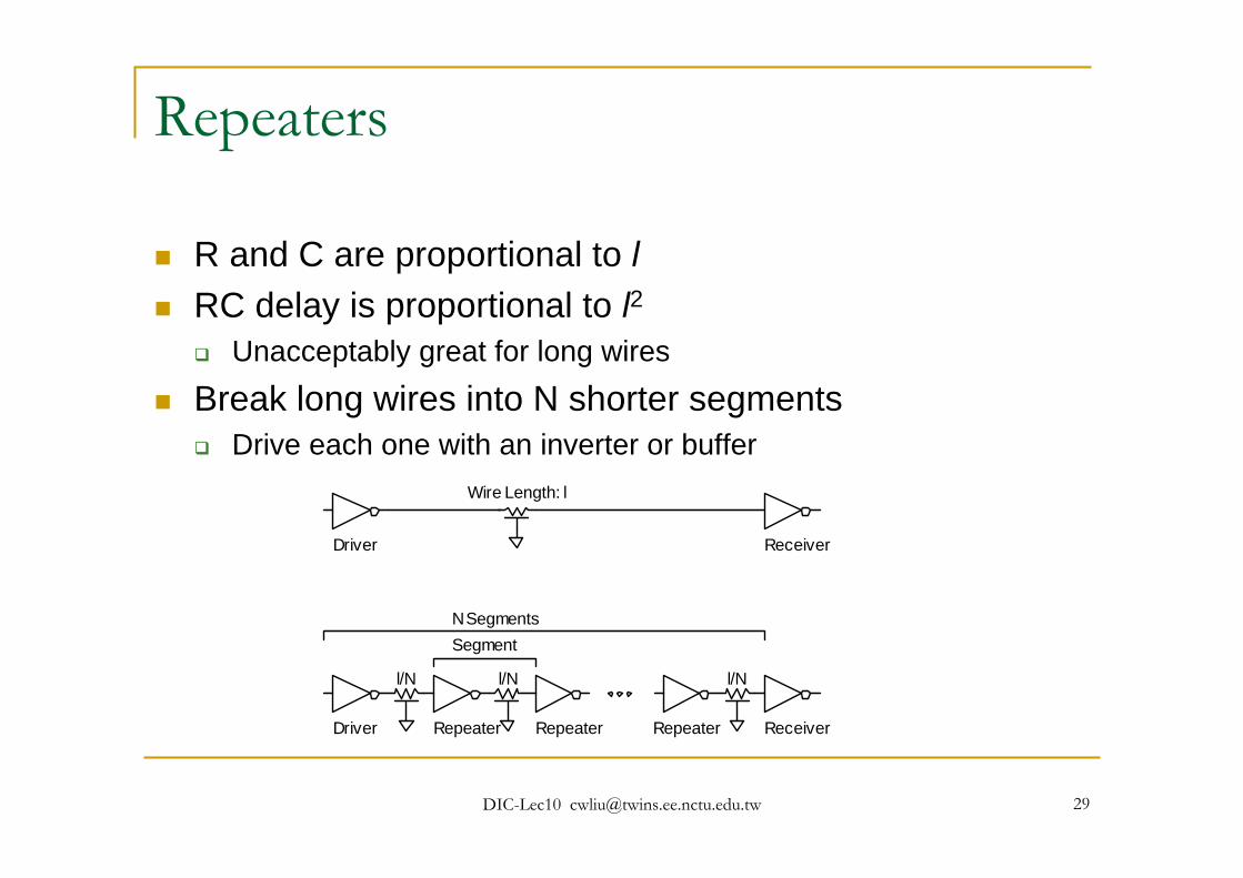
Repeaters
R and C are proportional to lRC delay is proportional to l2
Unacceptably great for long wires
Break long wires into N shorter segmentsDrive each one with an inverter or buffer
Wire Length: l
Driver Receiver
l/N
Driver
Segment
Repeater
l/N
Repeater
l/N
ReceiverRepeater
N Segments
DIC-Lec10 [email protected] 30
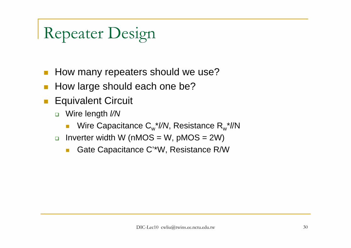
Repeater Design
How many repeaters should we use?How large should each one be?Equivalent Circuit
Wire length l/NWire Capacitance Cw*l/N, Resistance Rw*l/N
Inverter width W (nMOS = W, pMOS = 2W)Gate Capacitance C’*W, Resistance R/W
DIC-Lec10 [email protected] 31
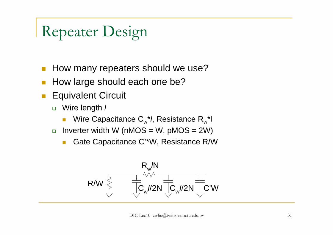
Repeater Design
How many repeaters should we use?How large should each one be?Equivalent Circuit
Wire length lWire Capacitance Cw*l, Resistance Rw*l
Inverter width W (nMOS = W, pMOS = 2W)Gate Capacitance C’*W, Resistance R/W
R/W C'WCwl/2N Cwl/2N
RwlN
DIC-Lec10 [email protected] 32
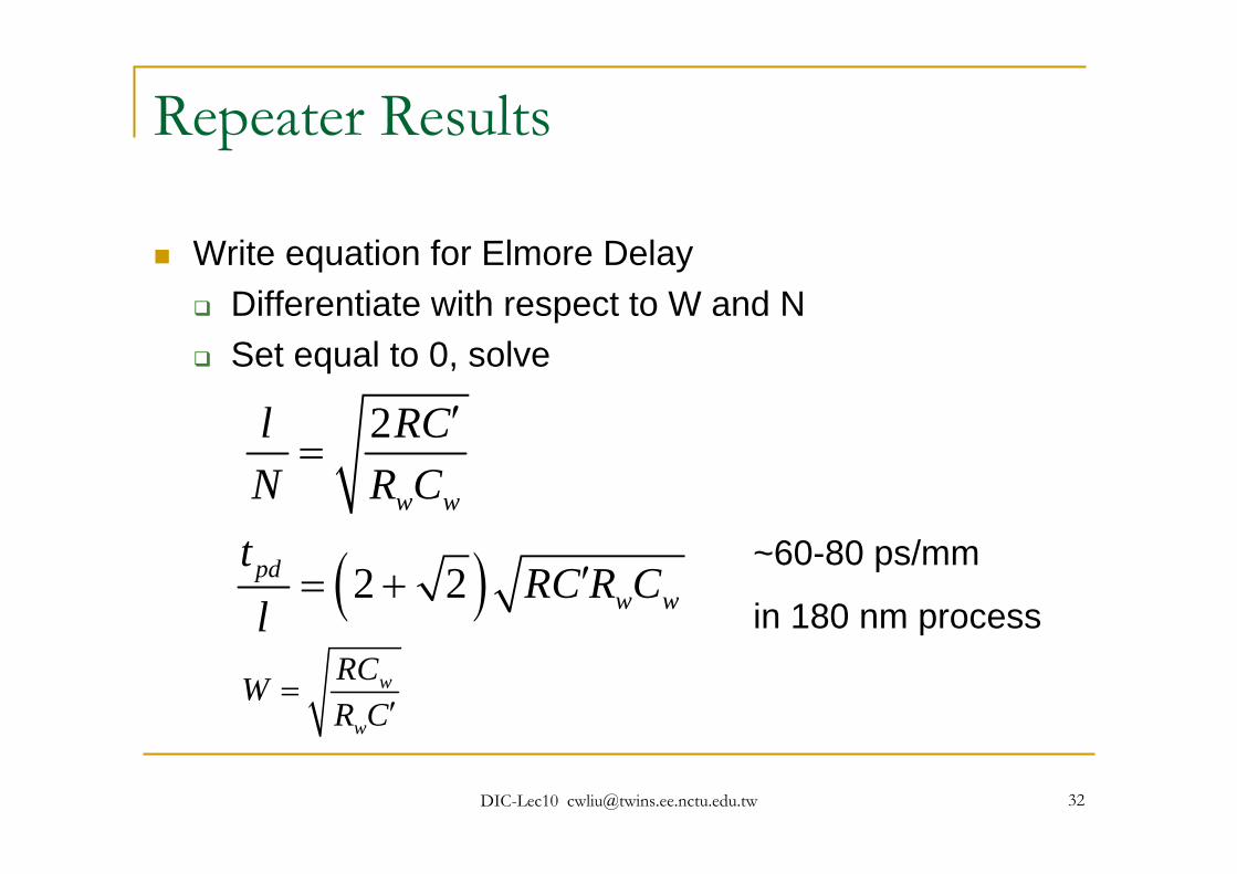
Repeater Results
Write equation for Elmore DelayDifferentiate with respect to W and NSet equal to 0, solve
2
w w
l RCN R C
′=
( )2 2pdw w
tRC R C
l′= +
w
w
RCWR C
=′
~60-80 ps/mm
in 180 nm process