
Digital implementation of a constant frequency hysteresis...
23
Turk J Elec Eng & Comp Sci (2016) 24: 4406 – 4428 c ⃝ T ¨ UB ˙ ITAK doi:10.3906/elk-1410-189 Turkish Journal of Electrical Engineering & Computer Sciences http://journals.tubitak.gov.tr/elektrik/ Research Article Digital implementation of a constant frequency hysteresis controller for dual mode operation of an inverter acting as a PV-grid interface and STATCOM Lenin PRAKASH * , Arutchelvi MEENAKSHI SUNDARAM, Kalyanraj DURAIRAJ Department of Electrical and Electronics Engineering, Saranathan College of Engineering, Tiruchirappalli, India Received: 31.10.2014 • Accepted/Published Online: 07.08.2015 • Final Version: 20.06.2016 Abstract: This paper presents a new constant frequency hysteresis current controller for the grid interface of a PV- fed three-phase voltage source inverter (VSI) for a dual mode operation, feeding real power during the daytime and reactive power alone during nights, thereby acting as a STATCOM. The constant frequency is inherently achieved by means of digital implementation in a simplified manner without any complex manipulations to choose a variable band width; rather the hysteresis band varies as a natural consequence of selecting appropriate constant sampling frequency. Analytical proof is presented for the switching frequency to remain constant, without compromising on the performance indices. The design of the proposed controller for a grid-connected inverter operating in dual mode is presented, along with simulation results. The proposed controller is successfully implemented using a 1.1 kW PV array-fed inverter. The hardware results presented show the grid current harmonics complies with IEEE 1547 and has been achieved in a simpler means when compared to other existing techniques. The proposed controller is expected to be an attractive solution for grid-connected inverter applications including distributed generation, power quality, and drive applications Key words: Hysteresis controller, constant frequency, grid-tied inverter, PV, STATCOM 1. Introduction The distributed generation concept, which was initiated a couple of decades back, has started slowly penetrating into most parts of the globe over the past decade and will sustain in the future as it paves the way for tapping renewable sources of energy spread geographically. Feeding power to the distribution grid from renewable sources like PV and fuel cells ranging from 1 kW to several MW has become operational in many countries. Different kinds of grid interfaces are already in use and still a lot of research is going on in this area. PV solar is turning out to be one of the attractive renewable sources used as a distributed generator (DG). The grid interface is essentially a power electronic inverter along with its associate control circuitry, although there are several other related topologies with inverter as a main component. The unique feature of the PV-fed inverter is that the same inverter can be operated as a STATCOM during the night for reactive power compensation to the grid [1–3]. With the increasing implementation of PV systems, it is becoming a promising idea to use the PV inverter as an active filter, for performing additional ancillary functions like harmonic compensation and power factor correction [4–9]. The other significant part in the grid interface is that the control algorithm is used for synchronizing the inverter with the grid and further facilitating maximum possible power flow from the DC link of the inverter. Normally, this control algorithm consists of two stages: the first one is the reference current generation stage, followed by a current control stage. * Correspondence: [email protected] 4406
Transcript of Digital implementation of a constant frequency hysteresis...

Turk J Elec Eng & Comp Sci
(2016) 24: 4406 – 4428
c⃝ TUBITAK
doi:10.3906/elk-1410-189
Turkish Journal of Electrical Engineering & Computer Sciences
http :// journa l s . tub i tak .gov . t r/e lektr ik/
Research Article
Digital implementation of a constant frequency hysteresis controller for dual
mode operation of an inverter acting as a PV-grid interface and STATCOM
Lenin PRAKASH∗, Arutchelvi MEENAKSHI SUNDARAM, Kalyanraj DURAIRAJDepartment of Electrical and Electronics Engineering, Saranathan College of Engineering, Tiruchirappalli, India
Received: 31.10.2014 • Accepted/Published Online: 07.08.2015 • Final Version: 20.06.2016
Abstract: This paper presents a new constant frequency hysteresis current controller for the grid interface of a PV-
fed three-phase voltage source inverter (VSI) for a dual mode operation, feeding real power during the daytime and
reactive power alone during nights, thereby acting as a STATCOM. The constant frequency is inherently achieved by
means of digital implementation in a simplified manner without any complex manipulations to choose a variable band
width; rather the hysteresis band varies as a natural consequence of selecting appropriate constant sampling frequency.
Analytical proof is presented for the switching frequency to remain constant, without compromising on the performance
indices. The design of the proposed controller for a grid-connected inverter operating in dual mode is presented, along
with simulation results. The proposed controller is successfully implemented using a 1.1 kW PV array-fed inverter. The
hardware results presented show the grid current harmonics complies with IEEE 1547 and has been achieved in a simpler
means when compared to other existing techniques. The proposed controller is expected to be an attractive solution for
grid-connected inverter applications including distributed generation, power quality, and drive applications
Key words: Hysteresis controller, constant frequency, grid-tied inverter, PV, STATCOM
1. Introduction
The distributed generation concept, which was initiated a couple of decades back, has started slowly penetrating
into most parts of the globe over the past decade and will sustain in the future as it paves the way for tapping
renewable sources of energy spread geographically. Feeding power to the distribution grid from renewable
sources like PV and fuel cells ranging from 1 kW to several MW has become operational in many countries.
Different kinds of grid interfaces are already in use and still a lot of research is going on in this area. PV solar
is turning out to be one of the attractive renewable sources used as a distributed generator (DG). The grid
interface is essentially a power electronic inverter along with its associate control circuitry, although there are
several other related topologies with inverter as a main component. The unique feature of the PV-fed inverter
is that the same inverter can be operated as a STATCOM during the night for reactive power compensation to
the grid [1–3]. With the increasing implementation of PV systems, it is becoming a promising idea to use the
PV inverter as an active filter, for performing additional ancillary functions like harmonic compensation and
power factor correction [4–9]. The other significant part in the grid interface is that the control algorithm is
used for synchronizing the inverter with the grid and further facilitating maximum possible power flow from the
DC link of the inverter. Normally, this control algorithm consists of two stages: the first one is the reference
current generation stage, followed by a current control stage.
∗Correspondence: [email protected]
4406

PRAKASH et al./Turk J Elec Eng & Comp Sci
This paper deals with the current control techniques used for a grid interfacing inverter. Several current
control techniques employed for a grid-connected inverter have been reported in the literature [10–14]. As
reported by a survey, some of the widely used current control strategies are linear current controllers, hysteresis
controllers, and digital dead beat controllers for a three-phase voltage source inverter. The survey also states
that the hysteresis controller exhibits superior performance especially for active filter application [15,16], which
has the advantages of robustness and fast dynamic response, while it has a disadvantage of variable as well as
high switching frequency. One of the commonly used linear controllers for distributed generation application
as stated by a survey [17], such as a PI current controller, suffers from a large steady state tracking error.
Although this tracking error could be minimized by increasing the bandwidth, it will push the system towards
its stability limits [18]. The PI controller also possesses the drawback of poor dynamic response, disturbance
rejection capability, and requiring accurate tuning to suit grid parameters [19,20].
The current control technique used in a grid-tied PV inverter must exhibit a fast dynamic response, if
it has to perform the role of active filter apart from feeding real power. Even for a STATCOM operation for
controlling local grid voltage, fast dynamic response becomes essential to achieve minimum voltage recovery
time [21]. Further, it is desirable to have a fast dynamic response while injecting real power to the grid to cope
with the power delivery requirement [22]. It is obvious that these grid interfacing inverters should have very
high efficiency, for which the current control strategy, which ultimately produces the gate pulses to the inverter,
plays a crucial role. Further, the current control strategy should ensure that the injected grid current complies
with the existing grid codes especially on harmonic limits. The other factor that contributes to efficiency is
the use of a transformer-less topology. A comparative study on a transformer-less topology for a grid tied
inverter revealed that three-phase full bridge split capacitor (3FB-SC) topology and three-phase neutral point
clamped (3×NPC) inverter are suitable for a grid connected application in terms of low leakage, efficiency,
and performance [23,24]. Though the 3×NPC topology exhibits better performance than the 3FB-SC, the
former needs twice the number of power switches and three times the number of diodes of the latter. This
paper presents the application of a hysteresis controller in a grid tied 3FB-SC transformer-less PV inverter, for
transacting real and reactive power, by exploiting its advantages of simplicity, robustness, and fast dynamic
response, as well as proposing a solution to overcome the drawback of variable switching frequency.
Several constant frequency hysteresis controllers have been already reported in the literature. For
example, [25] presents a ramp comparison constant frequency controller, which is a simple to implement
technique commonly used where constant frequency is desired; however, the current possesses high frequency
harmonics at regular multiples of carrier frequency. Moreover, additional compensation is required to reduce
the steady state error and achieve good command following sinusoidal reference current. Due to these factors its
application is limited to drives where the output current need not comply with grid regulations. [26] presents
an adaptive hysteresis control strategy for a drives system, in which the variable hysteresis band width is
predetermined based on the load equivalent impedances, while [27] proposes a similar technique in which the
hysteresis band is updated continuously based on load impedance, back emf, and supply voltage. The first
one is complicated to implement for grid connected inverter applications, while the next one needs the current
derivative information for predicting the next hysteresis band, which could not be accurately implemented due
to measurement noise. [28] proposes a fuzzy controller for a single-phase inverter based on the previous two
papers, and claims the complexity involved in the previous two papers has been minimized though not fully
eliminated. A constant sampling frequency method is proposed in [29] that once again depends on current error
derivative, but due to the complexity involved in finding current error derivative, a trial and error approach is
4407

PRAKASH et al./Turk J Elec Eng & Comp Sci
proposed to find the minimum sampling frequency. [30] proposes a strategy in which the third leg of the inverter
is applied with constant frequency pulses, which minimizes the variation in switching frequency but still does
not make it a constant value. [31] proposes a constant frequency hysteresis control scheme without bandwidth
control for a single-phase inverter, in which the values of reference and actual currents are predicted based on
the circuit parameters. Once again in this method the current derivative information is calculated continuously,
based on which the turn on time is calculated based on dc link voltage and inductance values. Further, it is
required to measure the turn off time. Though the method claims to give good results, the simplicity factor is
compromised to a large extent. Though several techniques are already reported, most of them are very complex
to implement with more computational burden, making them not suitable for real practice. In all the existing
schemes the successful operation of the advanced control techniques needs a highly accurate measurement and
feedback system, high speed processors with deep memory to meet the computational burden, and in some
cases additional circuitries. Hence, to ensure reliable operation, too many constraints need to be satisfied,
which introduces a hesitation and huddle for implementing this advanced technique for real time products and
practices.
This paper proposes a simple method that exploits all the advantages of the conventional hysteresis con-
troller but overcomes the major drawback, which is variable and high switching frequency, without compromising
any of the advantages, mainly the simplicity and robustness. In all the existing constant switching frequency
techniques the drawback of the conventional technique is eliminated at the cost of simplicity in implementation.
The proposed method employs a constant sampling frequency; it has been shown that by appropriate selection
of this sampling frequency the switching frequency is limited to one half of the sampling frequency and remains
constant at that value throughout. No extensive calculation is involved in finding the variable bandwidth, but
rather bandwidth changes as a natural consequence of selecting suitable constant sampling frequency. Moreover,
the maximum current ripple could be limited at desirable values. The design of the proposed control scheme has
been discussed in detail, which finally gives simple algebraic expressions for selection of sampling frequency with
an objective to achieve the desired performance indices: current ripple and current error. The other important
performance index, current THD, is inherently achieved and complies with IEEE 1547.
This paper is organized as follows. The conventional hysteresis current control scheme is presented in
section 2 to form a basis for the subsequent sections. The principle of operation of the proposed controller is
discussed in section 3. It is followed by a design procedure and stability analysis with an illustrative example,
considering a grid-tied inverter fed by a DG source, in section 4. The application of the proposed controller
for a grid-tied PV-STATCOM application is discussed in detail in section 5. This section presents the grid
interface topology along with complete control structure for boost converter and inverter for feeding real and
reactive power to the grid. The reference current generation algorithm for the inverter based on instantaneous
PQ theory is presented in section 5 along with simulation results. The digital implementation and hardware
validation results, along with comparison with published results and compliance to grid codes, are presented in
section 6.
2. Conventional hysteresis current control
The conventional hysteresis control technique is explained in this section to provide a basis to explain the
proposed control technique in the subsequent sections. This method controls the switches in an inverter
asynchronously to ramp the current through an inductor up and down so that it follows a reference. From
Figure 1a, if the actual current exceeds the upper hysteresis band (UHB), the upper device of the inverter is
turned off and the lower device is turned on. As the current decays and crosses the lower hysteresis band (LHB),
4408

PRAKASH et al./Turk J Elec Eng & Comp Sci
the lower device is turned off and the upper device is turned on. The equivalent circuit of one leg of the inverter
connected to a grid when the top switch is ON and the bottom switch is ON is shown in Figure 1b for different
extreme values of grid voltages (Vgn = 0, Vgn = Vg max , Vgn = –Vg max). The KVL of these two circuits
is given by Eq. (1), where ‘Vgn ’ is the instantaneous value of phase-neutral grid voltage, ‘Vg max ’ is the peak
value of phase-neutral grid voltage, and ‘Vdc ’ is equal to half of the dc link voltage ‘Vd ’ fed by the DG source
‘VDG ’. The time duration for which the current has a positive slope and a negative slope within a switching
period is given in Eq. (2). As shown in Figure 2 and by Eq. (3) the switching period and hence the frequency
varies within a power cycle as the grid voltage is a function of time. The maximum and minimum value of
switching period and frequency is given in Eqs. (4) and (5), respectively.
GRID
REFERENCECURRENT
ALGORITHM
Ia*
Ib*
Ic*
TO INVERTER’S IGBT GATETERMINAL
THREE PHASE INVERTER
S 1 S 3 S 5
S 4 S 6 S 2
C1
C2
A
B
C
La
Lb
Lc
DG
+
-
Ia*
Ib*
Ic*
Ia
Ib
Ic
S1
S4
S3
S6
S5
S2
VDG
VDG
Vd
ia
ibic
Vga
Vgb
Vgc
Distributed generator
source
HYSTERESIS CONTROLLER
When Top switch is ON V0_inv = Vdc
+ - ILL
Vdc Vgn
Vgn = 0
+ - ILL
Vdc Vgn
Vgn = 0
Vdc Vgn
Vgn = Vg_max
+ - ILL
Vdc Vgn
+ - ILL
+
-
+
-Vgn = Vg_max
Vgn
Vgn = --Vg_max
+ - ILL
Vgn
-
+
-
+Vgn = -Vg_max
Vdc
+ - ILL
Vdc
When Bottom switch is ON V0_inv = -Vdc
Figure 1. (a) Block diagram of conventional hysteresis control method employed in a DG-fed grid connected three-
phase VSI. (b) Equivalent circuit of one leg when the top and bottom switches conduct in a switching period for different
extremes of grid voltage values.
4409

PRAKASH et al./Turk J Elec Eng & Comp Sci
∆t1 ∆t
2 ∆t
1 ∆t2
T s1 T s2
Figure 2. Different intervals within a switching period of actual current with positive and negative slope.
∆i
∆t1=
Vdc − Vgn
L,∆i
∆t2=
Vdc + Vgn
L... (1)
∆t1 =∆i.L
Vdc − Vgn,∆t2 =
∆i.L
Vdc + Vgn... (2)
Ts = ∆t1 +∆t2, Fs =1
∆t1 +∆t2... (3)
Tsmax =2VdcL∆i
V 2dc − V 2
gmax
, Tsmin =2L∆i
Vdc... (4)
Fsmax =Vdc
2L∆i, Fsmin =
V 2dc − V 2
gmax
2LVdc∆i... (5)
3. Principle of operation of the proposed constant frequency hysteresis control
As explained in the previous section the switching frequency varies within a period of the grid voltage and it
reaches its maximum when the grid voltage reaches its zero value. The above scheme could be implemented
either using an analogue circuit or digitally using a digital signal processor (DSP). In the case of digital
implementation the actual current signals are sampled at regular intervals, compared with the reference, and
appropriate switching commands will be sent by the controller to the gates of the IGBTs. The proposed method
is digitally implemented and it can be shown that the switching frequency can be limited to half of the sampling
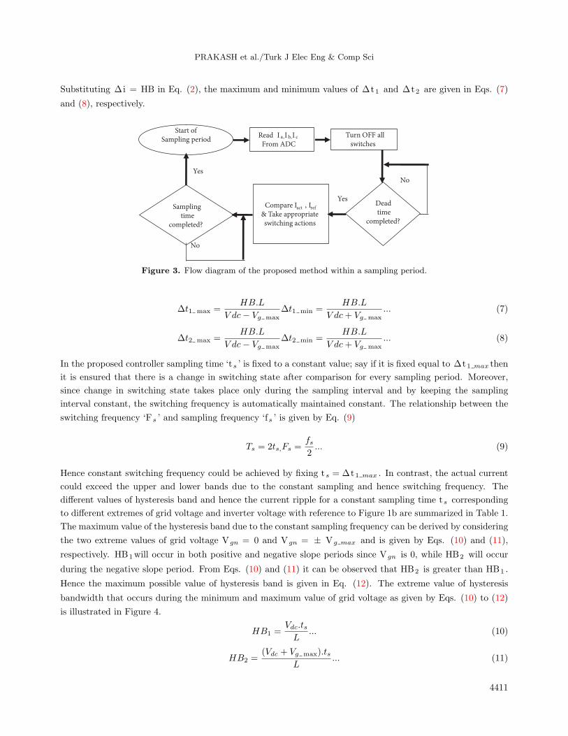
frequency by appropriate selection of the sampling frequency. Figure 3 shows the flow diagram of the proposed
control scheme in a sampling period. It can be observed that for every sampling period the comparisons are
done and appropriate switching actions are taken as given by Eq. (6). The comparison of actual and reference
currents and the corresponding switching action takes place only once in every sampling period. The top and
bottom switches of each leg of the inverters are complimentary. It can be observed when the actual current is
confined within the upper and lower band there is no change in switching action after comparison.
Iact > IUB → Bottom Switch ONIact < ILB → Top switch ONILB < Iact < IUB → No Change
... (6)
From Eq. (2) it can be observed that the time durations ∆t1 and ∆t2 are variable by themselves and ∆t1will
be always greater than ∆t2 . In addition, the change in current ∆i is nothing but the hysteresis band width.
4410
PRAKASH et al./Turk J Elec Eng & Comp Sci
Substituting ∆i = HB in Eq. (2), the maximum and minimum values of ∆t1 and ∆t2 are given in Eqs. (7)
and (8), respectively.
Read I a,I b,I c
From ADC
Turn OFF all switches
Compare Iact , Iref
& Take appropriate switching actions
Yes
NoYes
No
Start of Sampling period
Samplingtime
completed?
Deadtime
completed?
Figure 3. Flow diagram of the proposed method within a sampling period.
∆t1 max =HB.L
V dc− Vg max∆t1 min =
HB.L
V dc+ Vg max... (7)
∆t2 max =HB.L
V dc− Vg max∆t2 min =
HB.L
V dc+ Vg max... (8)
In the proposed controller sampling time ‘ts ’ is fixed to a constant value; say if it is fixed equal to ∆t1 max then
it is ensured that there is a change in switching state after comparison for every sampling period. Moreover,
since change in switching state takes place only during the sampling interval and by keeping the sampling
interval constant, the switching frequency is automatically maintained constant. The relationship between the
switching frequency ‘Fs ’ and sampling frequency ‘fs ’ is given by Eq. (9)
Ts = 2ts,Fs =fs2... (9)
Hence constant switching frequency could be achieved by fixing ts = ∆t1 max . In contrast, the actual current
could exceed the upper and lower bands due to the constant sampling and hence switching frequency. The
different values of hysteresis band and hence the current ripple for a constant sampling time ts corresponding
to different extremes of grid voltage and inverter voltage with reference to Figure 1b are summarized in Table 1.
The maximum value of the hysteresis band due to the constant sampling frequency can be derived by considering
the two extreme values of grid voltage Vgn = 0 and Vgn = ± Vg max and is given by Eqs. (10) and (11),
respectively. HB1will occur in both positive and negative slope periods since Vgn is 0, while HB2 will occur
during the negative slope period. From Eqs. (10) and (11) it can be observed that HB2 is greater than HB1 .
Hence the maximum possible value of hysteresis band is given in Eq. (12). The extreme value of hysteresis
bandwidth that occurs during the minimum and maximum value of grid voltage as given by Eqs. (10) to (12)
is illustrated in Figure 4.
HB1 =Vdc.tsL
... (10)
HB2 =(Vdc + Vg max).ts
L... (11)
4411

PRAKASH et al./Turk J Elec Eng & Comp Sci
Table 1. Different values of hysteresis band for a constant sampling time ‘ts ’ corresponding to different extremes of
grid and inverter voltage.
Grid voltage Inverter voltage vgn = 0 vgn = Vg max vgn = −Vg max
+Vdc HB = Vdc.tsL HB =
(Vdc−Vg max).tsL HB =
(Vdc+Vg max).tsL
–Vdc HB = Vdc.tsL HB =
(Vdc+Vg max).tsL HB =
(Vg max−Vdc).tsL
HB1
HBmax
∆t2_min
tsts =∆t1_max
HB
I UB
I LB
Iref
Iact
I LB_new
HB
Iact
I UB_new
∆t1 = ∆t2
ts
max_ggn VwhenV =
0=gnwhenV
HB - Bandwidth used for comparison in the programHBmax → Consequent maximum Bandwidth that occurs
∆t2 = ∆t1
ts
Figure 4. Maximum and minimum value of resultant hysteresis bands.
HB max = HB2 =(Vdc + Vg max).ts
L... (12)
Hence in the proposed scheme the switching frequency is maintained constant, while change in hysteresis
bandwidth occurs as a natural consequence of choosing appropriate sampling frequency, thereby making the
implementation very simple. Further, the maximum value of hysteresis band width for the given switching
frequency can be properly designed, which is explained in the subsequent section.
4. Design of constant frequency hysteresis controller
The design of interfacing a DG source into a 3-phase grid through a three-phase full bridge split capacitor VSI
is explained in this section. The following steps are followed in designing the proposed controller
1. The permissible switching frequency, which is based on the power semiconductor switch employed and the
allowable switching losses, is fixed to a desired value.
2. The inductor value is chosen by using Eq. (12) by substituting HBmax = ∆IMAX (maximum permissible
current ripple).
3. Calculate the sampling frequency using Eq. (9).
4. Since the sampling time should be equal to ∆t1 max , the hysteresis band width value that is used for
comparison (HB) and generating pulses as given by Eq. (6) is chosen based on the ∆IMAX .
5. Substitute HBmax = ∆IMAX in Eq. (12) and ∆t1 max = ts in Eq. (7); the value of HB is chosen by
Eq. (13)
4412

PRAKASH et al./Turk J Elec Eng & Comp Sci
HB =
(Vdc − Vg max
Vdc + Vg max
)∆IMAX ... (13)
IUB = Iref +HB
2and, ILB = Iref − HB
2... (14)
By selecting the value of hysteresis band (HB) as given by Eq. (13) and the upper and lower band by Eq. (14)
will actually make the maximum value of the variable hysteresis band equal to the maximum allowable ripple
current ∆Imax . The above procedure is illustrated with the following example. The power circuit arrangement
considered for design is shown in Figure 5. The circuit parameters considered are given in Table 2. The
calculated values of the circuit parameters are as follows: sampling frequency fs = 10 kHz, L = 37 mH, HB =
0.2. The analytically calculated and plotted current waveforms based on the proposed controller are shown in
Figure 6a. The calculated value at 30 degree interval within a half cycle of the grid voltage is listed in Table 3.
Figure 5. Simulation diagram showing the power circuit of the grid interface system. 4
Table 2. Parameters considered for design.
S. no. Parameters Symbol Unit Value
1 Grid phase voltage (rms) Vgn rms V 110
2 Grid frequency fg Hz 50
3 Allowable current ripple ∆IMAX Amps 0.9
4 DC link voltage Vd V 300
5 Switching frequency Fs Hz 5000
6 Nominal grid current (rms) Iref A 6
7 KVA rating of inverter Sinv KVA 2
4413
PRAKASH et al./Turk J Elec Eng & Comp Sci
Table 3. Current ripple and error within one half cycle.
Degree Vg(pu) Iref Iact ∆i Ierror
0 0.00 0.00 0.00 0.59 0.00
30 0.72 4.32 3.89 0.75 0.43
60 1.24 7.44 6.65 0.86 0.79
90 1.41 8.49 7.85 0.90 0.64
120 1.22 7.30 7.04 0.86 0.27
150 0.68 4.09 4.10 0.74 –0.01
180 0.00 0.00 0.59 0.59 –0.59
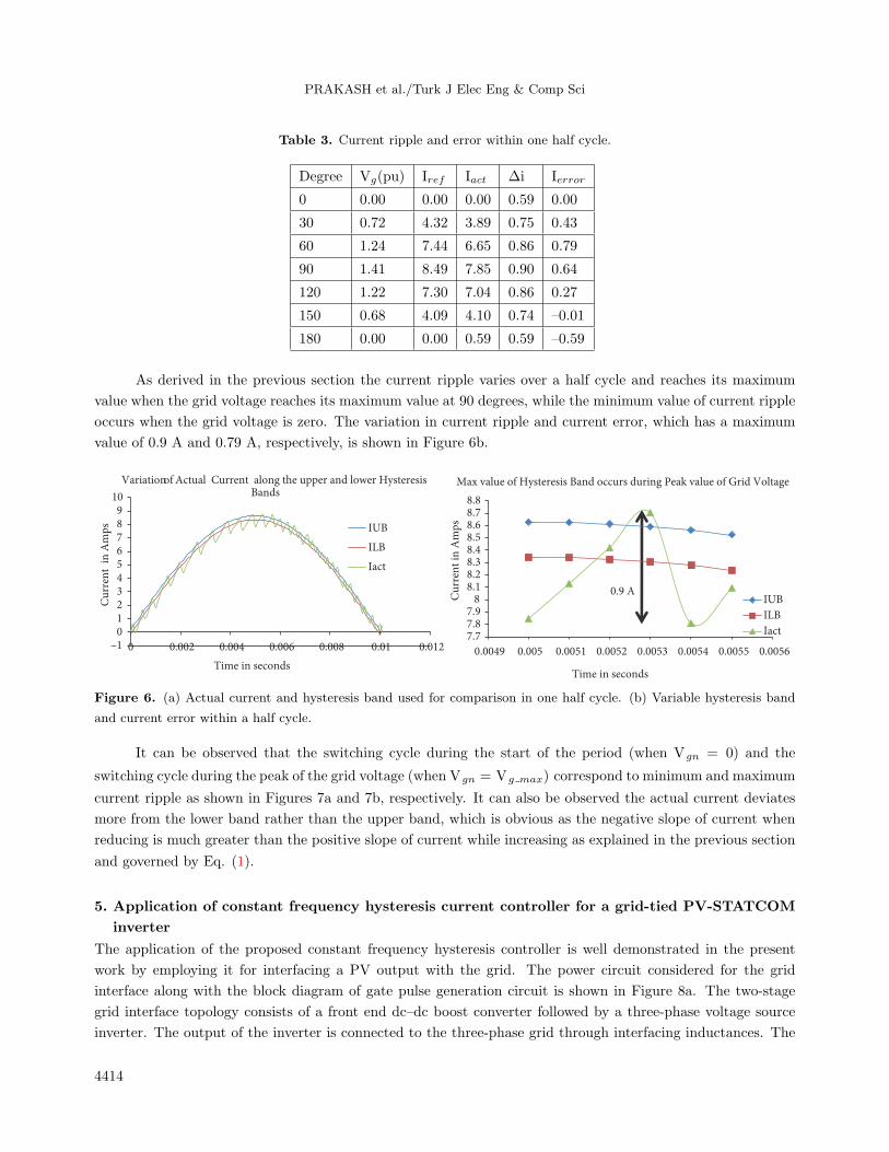
As derived in the previous section the current ripple varies over a half cycle and reaches its maximum
value when the grid voltage reaches its maximum value at 90 degrees, while the minimum value of current ripple
occurs when the grid voltage is zero. The variation in current ripple and current error, which has a maximum
value of 0.9 A and 0.79 A, respectively, is shown in Figure 6b.
–10123456789
10
0 0.002 0.004 0.006 0.008 0.01 0.012
IUB
ILB
Iact
Variationof Actual Current along the upper and lower Hysteresis Bands
Cu
rren
t i
n A
mp
s
Time in seconds
7.77.87.9
88.18.28.38.48.58.68.78.8
0.0049 0.005 0.0051 0.0052 0.0053 0.0054 0.0055 0.0056
IUB
ILB
Iact
Max value of Hysteresis Band occurs during Peak value of Grid Voltage
0.9 A
Time in seconds
Cu
rren
t in
Am
ps
Figure 6. (a) Actual current and hysteresis band used for comparison in one half cycle. (b) Variable hysteresis band
and current error within a half cycle.
It can be observed that the switching cycle during the start of the period (when Vgn = 0) and the
switching cycle during the peak of the grid voltage (when Vgn = Vg max) correspond to minimum and maximum
current ripple as shown in Figures 7a and 7b, respectively. It can also be observed the actual current deviates
more from the lower band rather than the upper band, which is obvious as the negative slope of current when
reducing is much greater than the positive slope of current while increasing as explained in the previous section
and governed by Eq. (1).
5. Application of constant frequency hysteresis current controller for a grid-tied PV-STATCOM
inverter
The application of the proposed constant frequency hysteresis controller is well demonstrated in the present
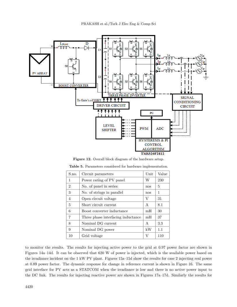
work by employing it for interfacing a PV output with the grid. The power circuit considered for the grid
interface along with the block diagram of gate pulse generation circuit is shown in Figure 8a. The two-stage
grid interface topology consists of a front end dc–dc boost converter followed by a three-phase voltage source
inverter. The output of the inverter is connected to the three-phase grid through interfacing inductances. The
4414

PRAKASH et al./Turk J Elec Eng & Comp Sci
–0.4
–0.2
0
0.2
0.4
0.6
0.8
1
1.2
1.4
1.6
1.8
0 0.0001 0.0002 0.0003 0.0004 0.0005 0.0006
I UB
I LB
Iact
Time in seconds
Cu
rren
t i
n A
mp
s
Min value of Current Ripple occurs during Grid Voltage Zero
0.6A
7.77.87.9
88.18.28.38.48.58.68.78.8
0.0049 0.005 0.0051 0.0052 0.0053 0.0054 0.0055 0.0056
IUB
ILB
Iact
Max value of Hysteresis Band occurs during Peak value of Grid Voltage
0.9 A
Time in seconds
Cu
rren
t in
A
mp
s
Figure 7. (a) Minimum current ripple occurring at zero crossing of voltage. (b) Maximum current ripple occurring at
maximum value of voltage.
GRID
REFERENCECURRENT
ALGORITHM
Ia*
Ib*
Ic*
TO INVERTER’S IGBT GATETERMINALS
THREE PHASE INVERTER
S 1 S 3 S 5
S 4 S 6 S 2
C1
C2
A
B
C
La
Lb
Lc
VDC
VDC
Vd
iga
igb
igc
Vga
Vgb
Vgc
vd*
vd
CONSTANT FREQUENCY HYSTERESIS CURRENT
CONTROLLER
D
PV
ARRAY
MPPTCONTROLLER
Vpv Ipv
BOOST CONVERTER
LBOOST
CBOOSTSBOOST
PIController
+-
∑
Ref Current comp-1
Ref Current comp-2
Constant Frequency Hysteresis Controller
GATE PULSES
*
gi*
grmsI*
guserφ
actabcgi __
*
1gi
*
guseri
*p
gabcv
DCV
*
DCV
gabcv
Ref Current comp-3gabcv
labci
*
__ filteractgi
Figure 8. (a) Power circuit and controller block diagram of PV-grid interface. (b) Block diagram of the control structure
of the grid interface.
4415

PRAKASH et al./Turk J Elec Eng & Comp Sci
boost converter is used to extract the maximum power from the PV array and is controlled by an MPPT
controller. The classical perturb and observe algorithm is used in the present work for the control of the boost
converter [32]. The block diagram of the control structure for the three-phase inverter is shown in Figure 8b.
The reference current for the inverter is generated by regulating the dc link of the inverter. Regulation of
DC link ensures that the power that is pumped to the DC link is transferred to the three-phase AC grid. An
additional user defined reference current component is added with the reference generated by the DC link PI
regulator. This user defined current (rms magnitude as well as phase) is added to test the controller for its
capability to inject desired reactive power for STATCOM operation. Further, it gives the flexibility to test and
validate the grid interface with the proposed controller, for injecting real power at any desired power factor.
The reference current is generated based on generalized pq theory [33] as given in Eqs. (15) to (17) with the
objective of regulating the dc link voltage, which is summed up with the user defined current to get the total
grid reference current. The reference grid current and actual current are compared and gate pulses are generated
based on the proposed hysteresis controller.
vgn =
vga
vgb
vgc
, ig =
iga
igb
igc
... (15)
i∗g = i∗g1 + i∗g user... (16)
ig1 =p∗.vgn
v2ga + v2gb + v2gc... (17)
The proposed controller for the PV grid interface is validated by simulation using MATLAB/Simulink and has
been presented in this section. The hardware implementation and validation are presented in the subsequent
section. The parameters considered for simulation are as follows: interfacing inductance per phase Labc = 37
mH, Vgnrms = 110 V, output of DG; Vd = 300 V. The different cases considered for validation of the proposed
scheme in dual mode operation including STATCOM are given in Table 4. The simulation results for case 1 and
case 2 are shown in Figure 9. In case 1, the grid current lags the voltage by 166 degrees and injects real power
supply to the grid. At 0.04 s, reference current is changed from 2 A to 3 A and is responded to by the controller
dynamically as shown in Figure 9a. The instantaneous power waveforms are shown in Figure 9b. Similarly the
response at 0.89 power factor is shown in Figures 9c and 9d. The simulation results for STATCOM mode for
injecting and absorbing reactive power are shown in Figure 10. It can be observed from the results that the
STATCOM current lags the grid voltage by 90 degrees, absorbing a reactive power of 1000 VAR as shown in
Figures 10a and 10b. In addition, the dc link voltage reaches its steady state value without any overshoot as
shown in Figure 10c. Similarly the response for STATCOM operation and zero pf leading injecting 700 VAR
to the grid is shown in Figures 10d–10f. Moreover, another study (case 5) has been considered in grid interface
mode to analyze the sensitivity of the controller to variation in inductance value. The variations in inductance
considered are ± 20% of the designed value. The simulation is performed for lower and upper extremes of
the designed inductance value. The injected grid current waveforms for nominal, lower extreme, and upper
extreme are shown in Figure 11. It can be observed that for all the values of inductances the performance of
the controller measured in terms of THD and current ripple has no significant variation and is well within the
permissible limits used in the design.
4416

PRAKASH et al./Turk J Elec Eng & Comp Sci
Table 4. Different case studies considered for validation of the proposed controller.
S.no. Mode Cases
Case 1 DG Interface Injection of real power to grid at 0.97 power factor
Case 2 DG Interface Injection of real power to grid at 0.89 power factor
Case 3 STATCOM Injection of reactive power to grid
Case 4 STATCOM Absorption of reactive power from grid
Case 5 DG Interface Test for parameter sensitivity :Injection of real power at UPF using ± 10% of designedvalue of interfacing inductances
Figure 9. (a) Three-phase grid voltage and currents at 0.97 power factor. (b) Injection of real power and reactive power
to the grid. (c) Three-phase grid voltage and currents at 0.89 power factor. (d) Injection of real power and reactive
power to the grid.
6. Digital implementation and hardware results
The proposed controller has been validated using a 1.1 kW PV array and the successful operation of the grid
interface mode as well as the STATCOM mode of operation has been demonstrated, along with performance
compliance to grid codes. The overall hardware block diagram of a PV-fed boost converter-fed three-phase
grid connected inverter is shown in Figure 12. A 1.1 kW PV array of panels is connected to a boost converter
4417

PRAKASH et al./Turk J Elec Eng & Comp Sci
Figure 10. STATCOM operation at zero power factor lag: (a) Three-phase grid voltage and currents. (b) Instantaneous
reactive power. (c) Response of DC link voltage. STATCOM operation at zero power factor lead: (d) Three-phase grid
voltage and currents. (e) Instantaneous reactive power. (f) Response of DC link voltage.
to get the desired link voltage for interfacing the PV output with the 110 V grid through a three-phase VSI
and interfacing inductors. Hall effect voltage and current sensors are used for sensing the grid voltage, dc
link voltage, and currents. Only two current and voltage sensors are used for sensing grid current and voltage,
respectively, considering a balanced system. A signal conditioner circuit is used for interfacing the sensor signals
(that is bipolar in nature) with the uni-polar ADC of the DSP and similarly a level-shifter followed by a driver
circuit is used to interface the 3.3 V PWM outputs of the DSP with the gates of the IGBTs. The circuit
parameters considered for hardware implementation are shown in Table 5. The complete control scheme is
digitally implemented using a DSP TMS320F2812. The ADC is configured to capture two analogue current
4418

PRAKASH et al./Turk J Elec Eng & Comp Sci
Figure 11. R phase grid current showing maximum current ripple and THD for different values of interfacing induc-
tances.
signals, two grid voltages, and dc link voltage at a sampling frequency of 10 kHz. Event Manager ‘A’ (EVA)
timer is used to set the sampling frequency at 10 kHz, which triggers the ADC for every sampling period and
seven PWM outputs from EVA are used to generate the gate signals for IGBTs of VSI and a boost converter.
For implementing the hysteresis controller, the PWM outputs are either forced low or forced high based on the
comparator results, which is achieved by configuring the action control register (ACTRA) of EVA. At the start
of each sampling time voltage and current signals are acquired and the reference currents and upper and lower
bands are calculated based on the reference current generation algorithm explained in the previous section.
The actual current is compared with the upper and lower bands and a decision is made to change the
switching pattern; further, all the switches are turned off for a few microseconds in order to introduce dead
time between the changing switching patterns, which ensures the switching frequency remains constant at half
of the sampling frequency at 5 kHz. The next sampling starts at the end of the current sampling time and it
creates a new switching pattern, and the cycle repeats. The proposed control scheme is validated considering
different cases that are used for simulation as mentioned in Table 4. The grid voltage, harmonic spectrum of
voltage, and injected grid current are shown in Figures 13a–13c, respectively. A power quality analyzer is used
4419
PRAKASH et al./Turk J Elec Eng & Comp Sci
Figure 12. Overall block diagram of the hardware setup.
Table 5. Parameters considered for hardware implementation.
S.no. Circuit parameters Unit Value
1 Power rating of PV panel W 230
2 No. of panel in series nos 5
3 No. of strings in parallel nos 1
4 Open circuit voltage V 31
5 Short circuit current A 8.1
6 Boost converter inductance mH 30
7 Three phase interfacing inductance mH 37
8 Nominal DG current A 3.3
9 Nominal DG power kW 1.1
10 Grid voltage V 110
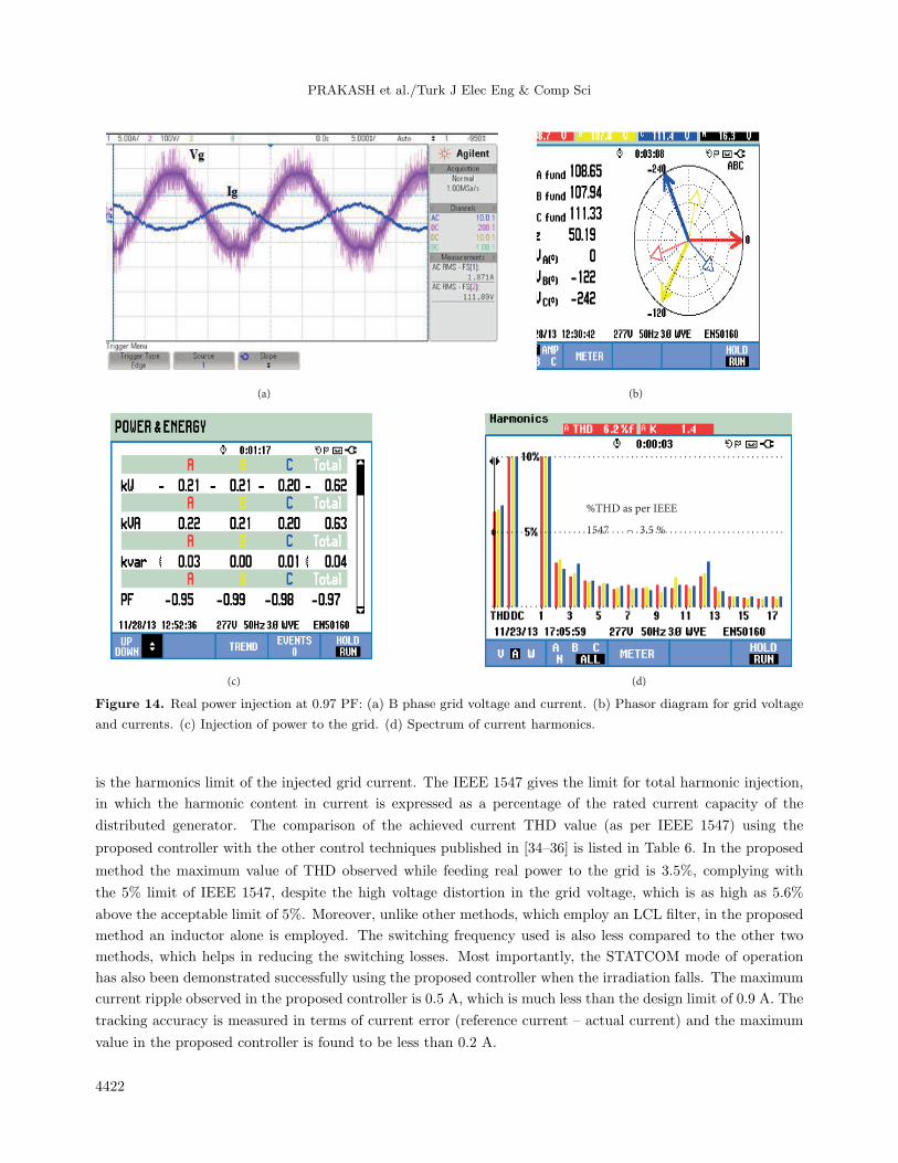
to monitor the results. The results for injecting active power to the grid at 0.97 power factor are shown in
Figures 14a–14d. It can be observed that 620 W of power is injected, which is the available power based on
the irradiance incident on the 1 kW PV plant. Figures 15a–15d show the results for case 2 injecting real power
at 0.89 power factor. The dynamic response for change in reference current is shown in Figure 16. The same
grid interface for PV acts as a STATCOM when the irradiance is low and there is no active power input to
the DC link. The results for injecting reactive power are shown in Figures 17a–17d. Similarly the results for
4420

PRAKASH et al./Turk J Elec Eng & Comp Sci
drawing reactive power are shown in Figures 18a–18c. The regulation of DC link voltage while operating as a
STATCOM is shown in Figures 19a and 19b. The switching frequency of gate pulses, which remains constant
throughout, is shown in Figure 20a.
(a) (b)
(c)
Figure 13. (a) Three-phase grid voltage waveform. (b) Harmonic spectrum of grid voltage. (c) Three-phase grid
currents for 3 A reference.
The reference currents generated by the DSP along with the actual currents read by the ADC are shown
in Figure 20b. It can be observed from the shape of the current that actual current follows the reference in a
more precise manner. Further, it can be observed that the reference current itself is not purely sinusoidal due
to the fact that the grid voltage itself contains distortion, which is reflected in the reference current as per Eq.
(26). The complete hardware setup of the 1.1 kW PV array with grid interface is shown in Figure 21. The
performance analysis of the proposed control scheme is discussed in the next section.
6.1. Comparison of results with other published techniques and compliance with grid codes
The performance comparison of the PV-STATCOM using the proposed controller with the other published
techniques as well as compliance with grid codes is presented in this section. IEEE 1547 gives the necessary
regulatory requirements to connect a distributed generator source to the grid. One of the important parameters
4421
PRAKASH et al./Turk J Elec Eng & Comp Sci
%THD as per IEEE
1547 – 3.5 %
(a) (b)
(c) (d)
Figure 14. Real power injection at 0.97 PF: (a) B phase grid voltage and current. (b) Phasor diagram for grid voltage
and currents. (c) Injection of power to the grid. (d) Spectrum of current harmonics.
is the harmonics limit of the injected grid current. The IEEE 1547 gives the limit for total harmonic injection,
in which the harmonic content in current is expressed as a percentage of the rated current capacity of the
distributed generator. The comparison of the achieved current THD value (as per IEEE 1547) using the
proposed controller with the other control techniques published in [34–36] is listed in Table 6. In the proposed
method the maximum value of THD observed while feeding real power to the grid is 3.5%, complying with
the 5% limit of IEEE 1547, despite the high voltage distortion in the grid voltage, which is as high as 5.6%
above the acceptable limit of 5%. Moreover, unlike other methods, which employ an LCL filter, in the proposed
method an inductor alone is employed. The switching frequency used is also less compared to the other two
methods, which helps in reducing the switching losses. Most importantly, the STATCOM mode of operation
has also been demonstrated successfully using the proposed controller when the irradiation falls. The maximum
current ripple observed in the proposed controller is 0.5 A, which is much less than the design limit of 0.9 A. The
tracking accuracy is measured in terms of current error (reference current – actual current) and the maximum
value in the proposed controller is found to be less than 0.2 A.
4422

PRAKASH et al./Turk J Elec Eng & Comp Sci
(a)(b)
(c) (d)
Figure 15. Real power injection at 0.89 power factor: (a) B phase grid voltage and current. (b) Phasor diagram for
grid voltage and current. (c) Injection of power to the grid. (d) Spectrum of current harmonics.
Figure 16. Three-phase grid current with reference change from 3 A to 2 A.
4423

PRAKASH et al./Turk J Elec Eng & Comp Sci
Table 6. Performance comparison of different control techniques for a grid tied PV system with the proposed controller.
System
considered for
validation
Control technique
Interfacing
components with
grid
Current THD
as per IEEE
1547
Voltage
THD
Switching
frequency
1.2 kW grid tied
PV system
Stepped inductor
control with variable
hysteresis band width
control
Stepped variable
inductor < 5% NM* 2 kHZ
5 kW grid tied
PV system
Adaptive dead time
compensation LCL filter 1.40% NM* 15 kHZ
1.5 kW DC
source fed grid
tied inverter
Proportional resonant
current controller
with LCL filter
LCL filter 1.20% 2% 8.19 kHZ
1.1 kW grid tied
PV system
Proposed constant
frequency hysteresis
control
Inductor 3.50% 5.60% 5 kHz
*NM - Not mentioned
%THD as per IEEE
1547 – 4.1 %
(a)(b)
(c) (d)
Figure 17. STATCOM operation at 90 degree lagging: (a) B phase grid voltage and current. (b) Phasor diagram for
grid voltage and currents. (c) Injection of reactive power to the grid. (d) Harmonic spectrum of grid current.
4424
PRAKASH et al./Turk J Elec Eng & Comp Sci
(a) (b)
(c)
Figure 18. STATCOM operation at 90 degree leading: (a) B phase grid voltage and current. (b) Phasor diagram for
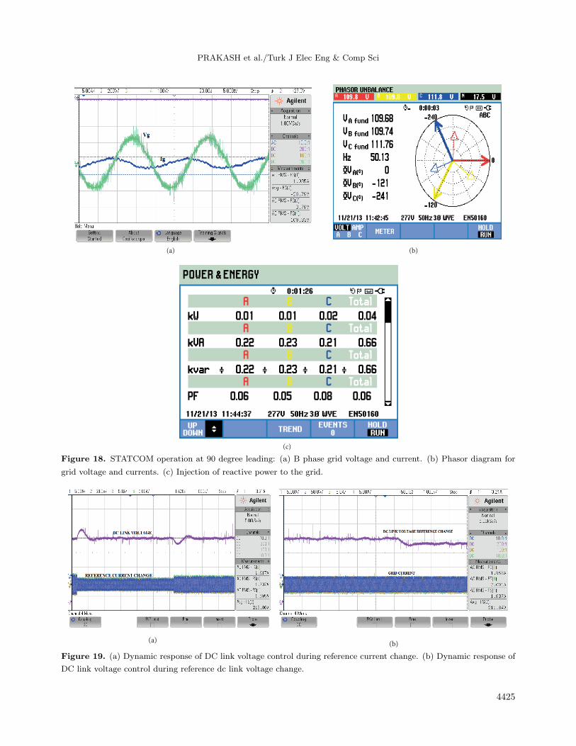
grid voltage and currents. (c) Injection of reactive power to the grid.
(a)(b)
Figure 19. (a) Dynamic response of DC link voltage control during reference current change. (b) Dynamic response of
DC link voltage control during reference dc link voltage change.
4425

PRAKASH et al./Turk J Elec Eng & Comp Sci
(a) (b)
Figure 20. (a) GATE pulses with 5 kHz constant switching frequency. (b) Reference current generated by the DSP
and the actual currents read by the ADC.
3
2
7
4
8
6
5
1
9
Figure 21. Hardware setup of the 1.1 kW PV-fed grid-connected inverter system.
7. Conclusion
A new constant frequency hysteresis current controller for the grid interface of a PV-fed three-phase VSI for a
dual mode operation, feeding real power during the daytime and reactive power alone during the night thereby
acting as a STATCOM has been presented. It has been shown that constant frequency has been inherently
achieved, by means of digital implementation in a simplified manner without any complex manipulations,
in such a way that the hysteresis band varies as a natural consequence of selecting appropriate constant
sampling frequency. The design procedure has been discussed in detail with an illustrative example along
with the simulation results. The proposed controller has been successfully implemented and validated using
DSP TMS320F2812 for a 1.1 kW PV array fed inverter, feeding real power and reactive power to the grid during
the day and night, respectively. The hardware results shows the controller is capable of tracking the reference
current accurately in both modes of operation while feeding real and reactive power to the grid from zero power
4426

PRAKASH et al./Turk J Elec Eng & Comp Sci
factor to unity power factor. In addition, compared with the other methods reported in the literature, the
proposed method achieves better performance by a much simpler means, also without any capacitor filter and
a low switching frequency, thereby achieving low switching losses. The result shows the proposed controller is
a simple, realistic, and attractive solution for a grid interface, especially for a PV-STATCOM inverter. It is
evident from the results that the proposed controller meets the complimentary objective of meeting enhanced
performance as well as ease of implementation.
References
[1] Varma RK, Siavashi EM, Das B, Sharma V. Novel application of a PV solar plant as STATCOM (PV-STATCOM)
during night and day in a distribution utility network part2. In: IEEE 2012 PES Transmission and Distribution
Conference; 7–10 May 2012; Orlando, FL, USA. New York, NY, USA: IEEE. pp. 1-8.
[2] Varma RK, Das B, Axente I, Vanderheide T. Optimal 24-hr utilization of a PV solar system as STATCOM (PV
STATCOM) in a distribution network. In: IEEE 2011 POWER ENG SOC; 24–29 July 2011; San Diego, CA, USA.
New York, NY, USA: IEEE. pp. 1-8.
[3] Varma RK, Khadkikar V, Seethapathy R. Night time application of PV solar farm as STATCOM to regulate grid
voltage. IEEE T Energy Conver 2009; 24: 983-985.
[4] Kuo YC, Liang TJ, Chen JF. A high-efficiency single-phase three-wire photovoltaic energy conversion system. IEEE
T Ind Electron 2003; 50: 116-122.
[5] Wu TF, Nien HS, Shen CL, Ming T. A single-phase inverter system for PV power injection and active power filtering
with nonlinear inductor consideration. IEEE T Ind Appl 2005; 4: 1075-1083.
[6] Wu TF, Nien HS, Hsieh HM, Shen CL. PV power injection and active power filtering with amplitude-clamping and
amplitude-scaling algorithms. IEEE T Ind Appl 2007; 43: 731-741.
[7] Lee TL, Li JC, Cheng PT. Discrete frequency tuning active filter for power system harmonics. IEEE T Power Electr
2009; 24: 1209-1217.
[8] Wang X, Zhuol F, Li J, Wang L, Ni S. Modeling and control of dual-stage high-power multifunctional PV system
in d–q–o coordinate. IEEE T Ind Electron 2013; 60: 1556-1570.
[9] Dogan H, Akkaya R. A control scheme employing an adaptive hysteresis current controller and an uncomplicated
reference current generator for a single-phase shunt active power filter. Turk J Elec Eng & Comp Sci 2014; 22:
1085-1097.
[10] Brod David M, Novonty DW. Current control of VSI pwm inverters. IEEE T Ind Appl 1985; 21: 562-570.
[11] Kazmierkowski MP, Malesani L. Current control techniques for three phase voltage source PWM converters. IEEE
T Ind Electron 1998; 45: 691-703.
[12] Moreno JC, Huerta JME, Gil RG, Gonzalez SA. A robust predictive current control for three-phase grid-connected
inverters. IEEE T Ind Electron 2009; 56: 1993-2004.
[13] Rahman KM, Khan MR, Choudhury MA, Rahman MA. Variable band hysteresis current controllers for PWM
voltage source inverters. IEEE T Power Electr 1997; 12: 964-970.
[14] Yao Z, Xiao L. Control of single-phase grid-connected inverters with nonlinear loads. IEEE T Ind Electron 2011;
60: 1384-1389.
[15] Kazmierkowski MP, Malesani L. Current control techniques for three-phase voltage-source PWM converters: a
survey. IEEE T Ind Electron 1998; 45: 691-703.
[16] Buso S, Malesani L, Mattavelli P. Comparison of current control techniques for active filter applications. IEEE T
Ind Electron 1998; 45: 722-729.
[17] Holmes DG, Lipo TA, McGrath BP, Kong WY. Optimized design of stationary frame three phase AC current
regulators. IEEE T Power Electr 2009; 24: 2417-2426.
4427

PRAKASH et al./Turk J Elec Eng & Comp Sci
[18] Yang S, Lei Q, Peng FZ, Qian Z. A robust control scheme for grid-connected voltage-source inverters. IEEE T Ind
Electron 2011; 58: 202-212.
[19] Shen G, Xu D. An improved control strategy for grid-connected voltage source inverters with an LCL filter. IEEE
T Power Electr 2008; 23: 1899-1906.
[20] Kojabadi HM, Bin Yu, Gadoura IA, Liuchen Chang, Ghribi M. A novel DSP-based current-controlled PWM strategy
for single phase grid connected inverters. IEEE T Power Electr 2006; 21: 985-993.
[21] Mohamed YA-RI, EI-Saadany EF. A control method of grid-connected PWM voltage source inverters to mitigate
fast voltage disturbances. IEEE T Power Syst 2009; 24: 489-491.
[22] Wang F, Duarte JL, Hendrix MAM. Design and analysis of active power control strategies for distributed generation
inverters under unbalanced grid faults. IET Gener Transm Dis 2010; 4: 905-916.
[23] Teodorescu R, Liserre M. Grid Converters for Photovoltaic and Wind Power Systems. 2nd ed. New York, NY, USA:
Wiley, 2011.
[24] Kerekes T, Teodorescu R, Klumpner C, Sumner M. Evaluation of three-phase transformer less photovoltaic inverter
topologies. IEEE T Power Electr 2009; 24: 2202-2211.
[25] Azizur Rahman M, Radwan TS, Osheiba AM, Lashine AE. Analysis of current controllers for voltage-source inverter.
IEEE T Ind Electron 1997; 44: 477-485.
[26] Bose BK. An adaptive hysteresis-band current control technique of a voltage-fed PWM inverter for machine drive
system. IEEE T Ind Electron 1990; 37: 402-408.
[27] Malesani L. Rossetto L, Tomasin P, Zuccato A. Digital adaptive hysteresis control with clocked commutation and
wide operating range. IEEE T Ind Appl 1996; 32: 316-325.
[28] Pereira RR, Da Silva CH, Cavalcanti LEM, Da Silva LEB, Lambert-Torres G, Ahn SU, Pinto JOP, Bose BK. A
simple full digital adaptive current hysteresis control with constant modulation frequency for active power filters.
In: IEEE International Conference on Industrial Applications Annual Meet; 23–27 September 2007; New Orleans,
LA, USA. New York, NY, USA: IEEE. pp. 1644-1648.
[29] Pan CT, Huang YS, Li CY. An error bounded current controller with constant sampling frequency. IEEE T Power
Electr 2004; 19: 739-747.
[30] George V, Mishra MK. Design and analysis of user-defined constant switching frequency current-control-based
four-leg DSTATCOM. IEEE T Power Electr 2009; 24: 2148-2158.
[31] Ho CNM, Cheung VSP, Chung HSH. Constant-frequency hysteresis current control of grid-connected VSI without
bandwidth control. IEEE T Power Electr 2009; 24: 2484-2495.
[32] Femia N, Petrone G, Spagnuolo G, Vitelli M. Optimization of perturb and observe maximum power point tracking
method. IEEE T Power Electr 2009; 20: 963-973.
[33] Peng FZ, Lai JS. Generalized instantaneous reactive power theory for three-phase power systems. IEEE Instrum
Meas 1996; 45: 293-297.
[34] Herran MA, Fischer JR, Gonzalez SA, Judewicz MG. Adaptive dead-time compensation for grid-connected PWM
inverters of single-stage PV systems. IEEE T Power Electr 2013; 28: 2816-2825.
[35] Wandhare RG, Agarwal V. A novel technique for THD control in grid connected photovoltaic systems using step
variable inductor approach. In: IEEE 35th Photovoltaic Specialists Conference (PVSC); 20–25 June 2010; Honolulu,
HI, USA. New York, NY, USA: IEEE. pp. 2844-2848.
[36] Kerekes T, Lungeanu M, Nakhost P, Teodorescu R, Andersen GK, Liserre M. Low-cost digital implementation
of proportional-resonant current controllers for PV inverter applications using delta operator. IEEE 31st Annual
Conference of Industrial Electronics Society; 6–10 Nov 2005; Raleigh, NC, USA. New York, NY, USA: IEEE. pp.
1-10.
4428