
Digital Fundamentalselectronics.physics.helsinki.fi/wp-content/uploads/2012/01/luento10.pdf ·...
51
Digital Fundamentals 1 Shift registers
Transcript of Digital Fundamentalselectronics.physics.helsinki.fi/wp-content/uploads/2012/01/luento10.pdf ·...

Digital Fundamentals
1
Shift registers
Objectives
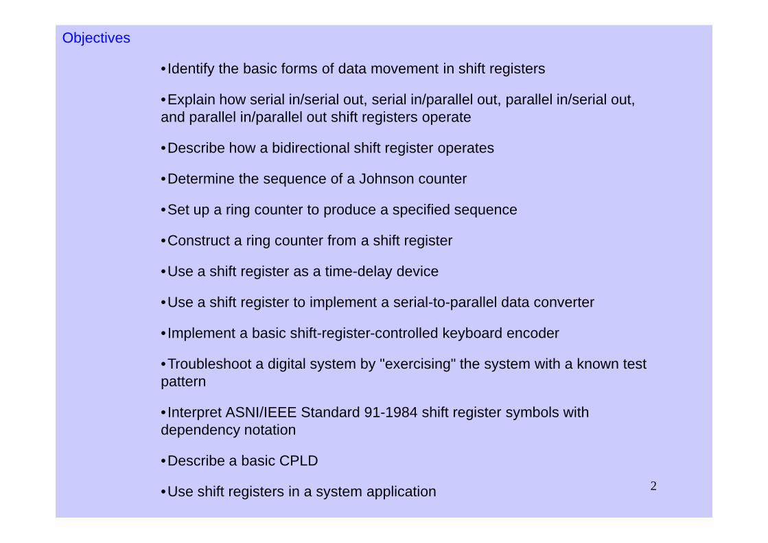
•Identify the basic forms of data movement in shift registers
•Explain how serial in/serial out, serial in/parallel out, parallel in/serial out, and parallel in/parallel out shift registers operate
•Describe how a bidirectional shift register operates
•Determine the sequence of a Johnson counter
•Set up a ring counter to produce a specified sequence
•Construct a ring counter from a shift register
•Use a shift register as a time-delay device
2
•Use a shift register as a time-delay device
•Use a shift register to implement a serial-to-parallel data converter
•Implement a basic shift-register-controlled keyboard encoder
•Troubleshoot a digital system by "exercising" the system with a known test pattern
•Interpret ASNI/IEEE Standard 91-1984 shift register symbols with dependency notation
•Describe a basic CPLD
•Use shift registers in a system application
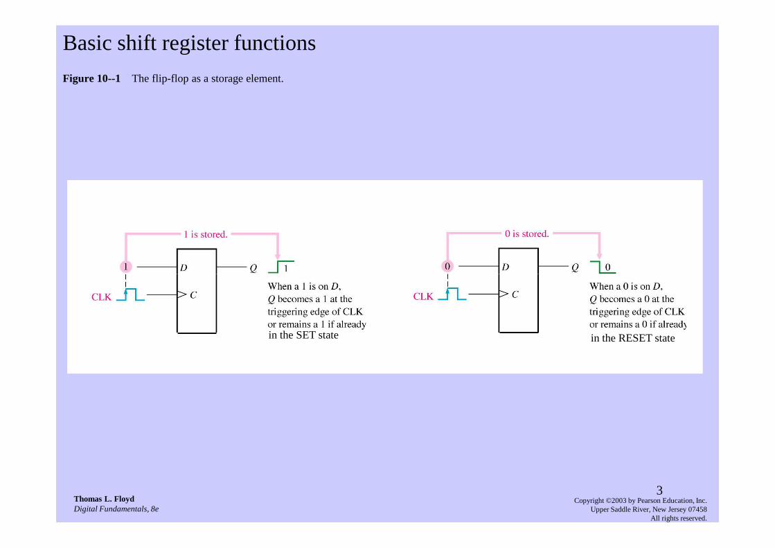
Figure 10--1 The flip-flop as a storage element.
Basic shift register functions
3Thomas L. FloydDigital Fundamentals, 8e
Copyright ©2003 by Pearson Education, Inc.Upper Saddle River, New Jersey 07458
All rights reserved.
in the SET state in the RESET state
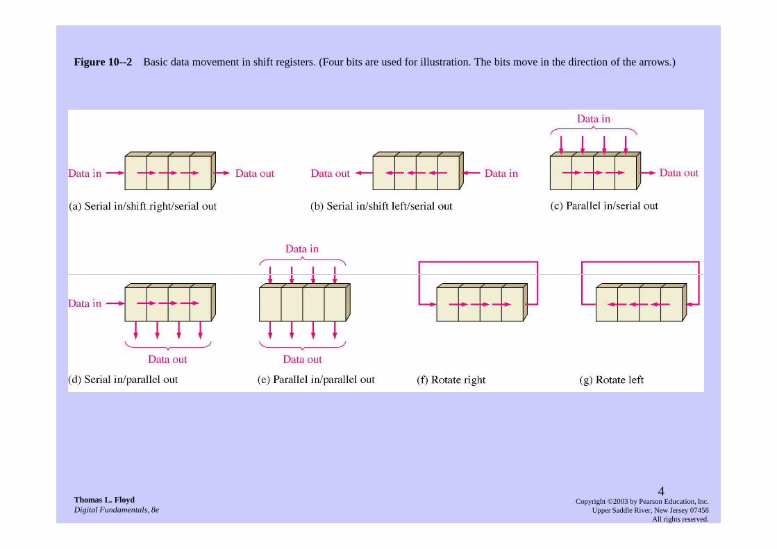
Figure 10--2 Basic data movement in shift registers. (Four bits are used for illustration. The bits move in the direction of the arrows.)
4Thomas L. FloydDigital Fundamentals, 8e
Copyright ©2003 by Pearson Education, Inc.Upper Saddle River, New Jersey 07458
All rights reserved.
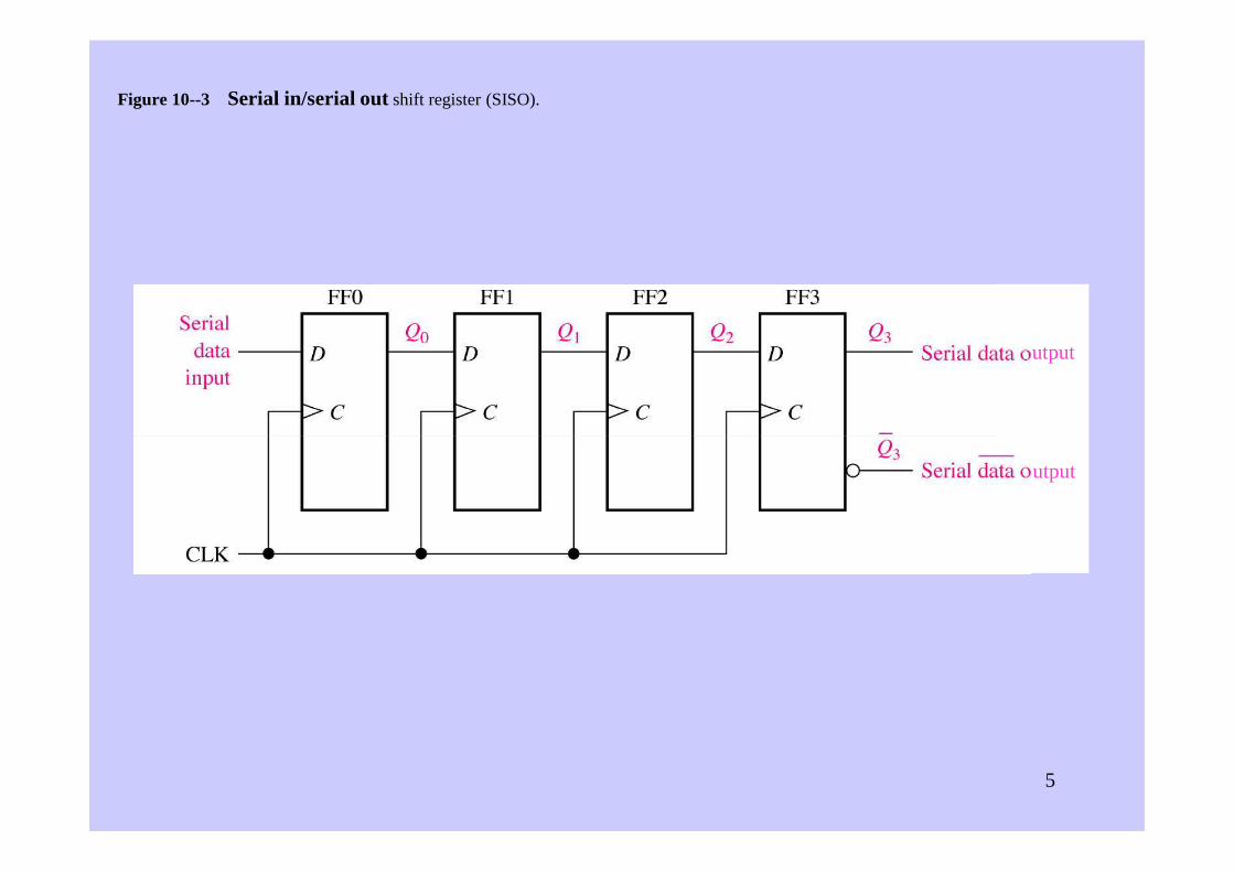
Figure 10--3 Serial in/serial outshift register (SISO).
utput
5
utput
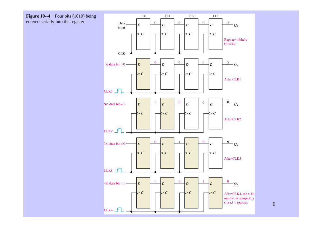
Figure 10--4 Four bits (1010) being entered serially into the register.
6

Figure 10--5 Four bits (1010) beingserially shifted out of the register andreplaced by all zeros.
7

Figure 10-6Example 10-1: Show the states for the specified data input and clock waveforms. Open file F10-06 to verify operation.
8Thomas L. FloydDigital Fundamentals, 8e
Copyright ©2003 by Pearson Education, Inc.Upper Saddle River, New Jersey 07458
All rights reserved.

Figure 10--7 Logic symbolfor an 8-bit serial in/serial out shift register (SISO).
9Thomas L. FloydDigital Fundamentals, 8e
Copyright ©2003 by Pearson Education, Inc.Upper Saddle River, New Jersey 07458
All rights reserved.
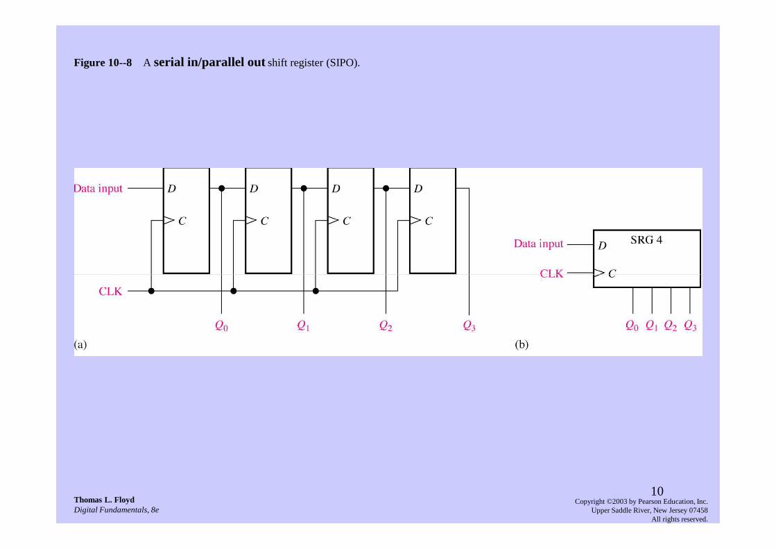
Figure 10--8 A serial in/parallel out shift register (SIPO).
10Thomas L. FloydDigital Fundamentals, 8e
Copyright ©2003 by Pearson Education, Inc.Upper Saddle River, New Jersey 07458
All rights reserved.

Figure 10-9 Example 10-2: Show the states of the 4-bit register (SRG 4). The register initially contains all 1s.
11Thomas L. FloydDigital Fundamentals, 8e
Copyright ©2003 by Pearson Education, Inc.Upper Saddle River, New Jersey 07458
All rights reserved.

Figure 10--10 The 74HC1648-bit serial in/parallel out shift register (SIPO).
12Thomas L. FloydDigital Fundamentals, 8e
Copyright ©2003 by Pearson Education, Inc.Upper Saddle River, New Jersey 07458
All rights reserved.
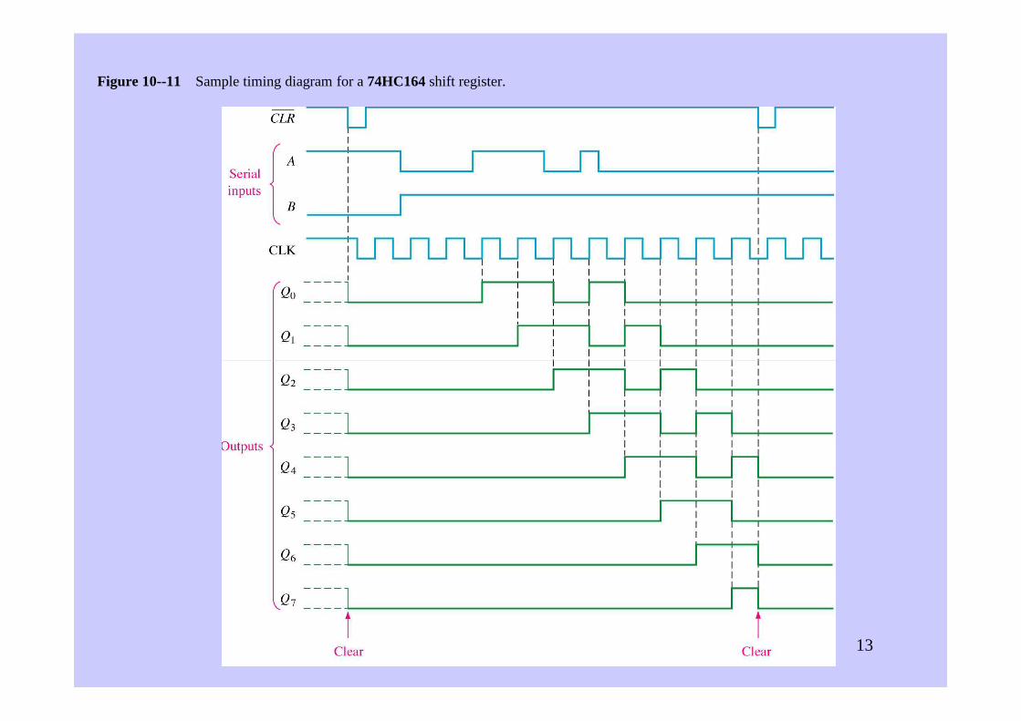
Figure 10--11 Sample timing diagram for a 74HC164shift register.
13
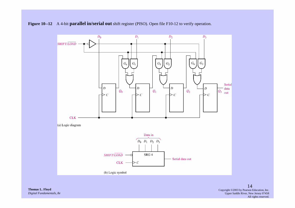
Figure 10--12 A 4-bit parallel in/serial out shift register (PISO). Open file F10-12 to verify operation.
14Thomas L. FloydDigital Fundamentals, 8e
Copyright ©2003 by Pearson Education, Inc.Upper Saddle River, New Jersey 07458
All rights reserved.

Figure 10-13 Example 10-3: Show the data-output waveform for a 4-bit register.
15Thomas L. FloydDigital Fundamentals, 8e
Copyright ©2003 by Pearson Education, Inc.Upper Saddle River, New Jersey 07458
All rights reserved.
i.e. the LSB
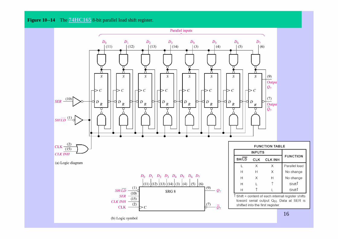
Figure 10--14 The 74HC1658-bit parallel load shift register.
16
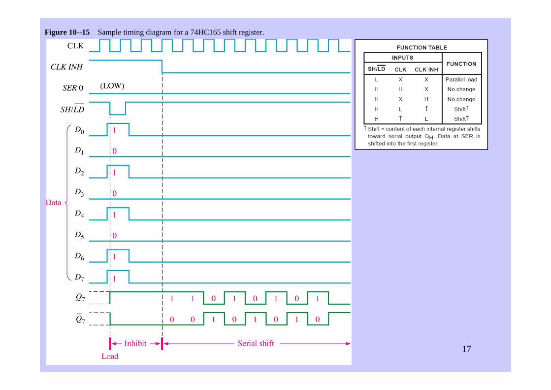
Figure 10--15 Sample timing diagram for a 74HC165 shift register.
17

Figure 10--16 A parallel in/parallel out register (PIPO).
18Thomas L. FloydDigital Fundamentals, 8e
Copyright ©2003 by Pearson Education, Inc.Upper Saddle River, New Jersey 07458
All rights reserved.
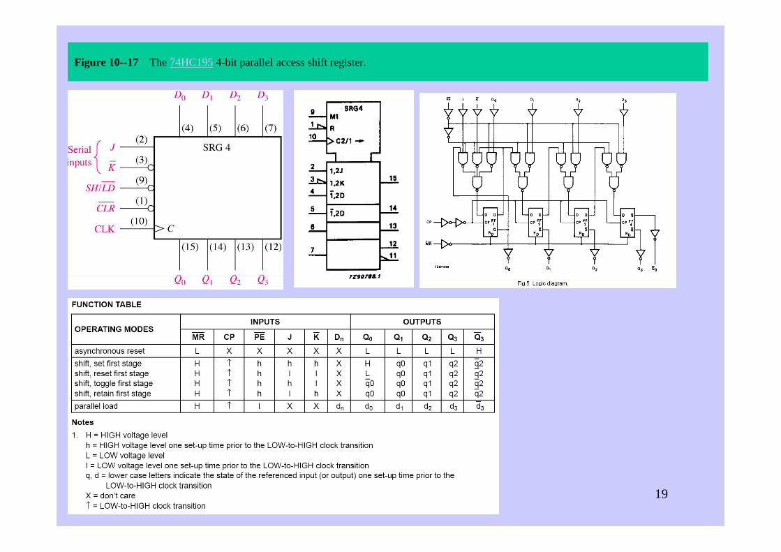
Figure 10--17 The 74HC1954-bit parallel access shift register.
19
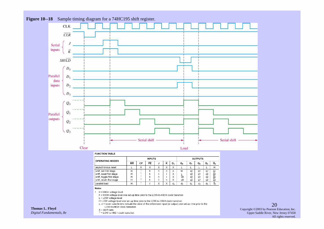
Figure 10--18 Sample timing diagram for a 74HC195 shift register.
20Thomas L. FloydDigital Fundamentals, 8e
Copyright ©2003 by Pearson Education, Inc.Upper Saddle River, New Jersey 07458
All rights reserved.
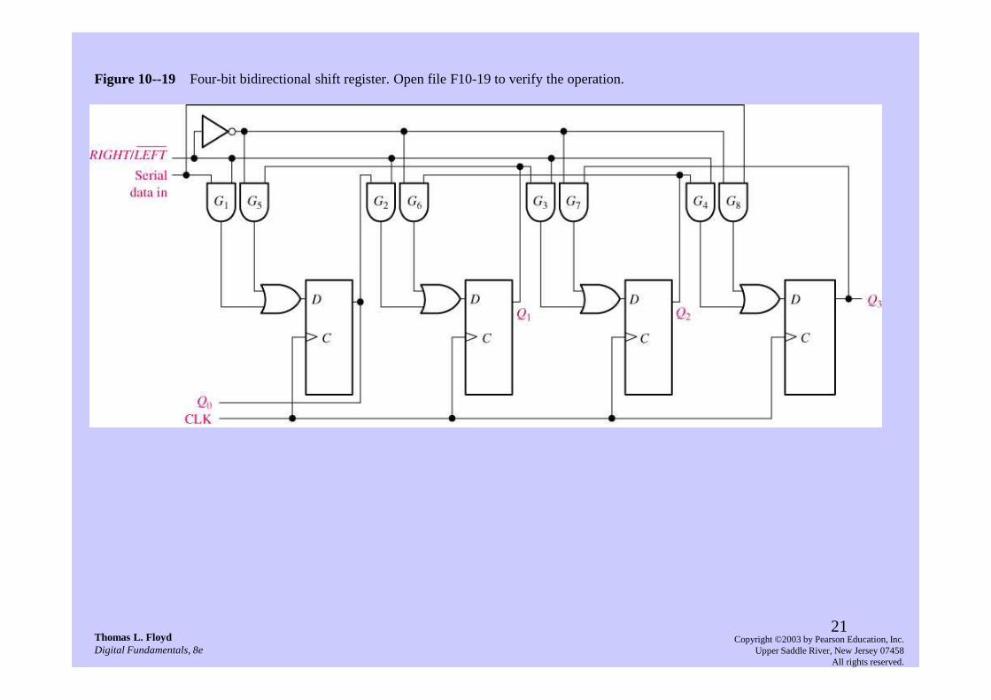
Figure 10--19 Four-bit bidirectional shift register. Open file F10-19 to verify the operation.
21Thomas L. FloydDigital Fundamentals, 8e
Copyright ©2003 by Pearson Education, Inc.Upper Saddle River, New Jersey 07458
All rights reserved.
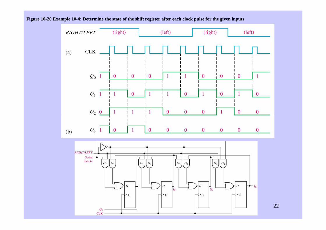
Figure 10-20 Example 10-4: Determine the state of the shift register after each clock pulse for the given inputs
22
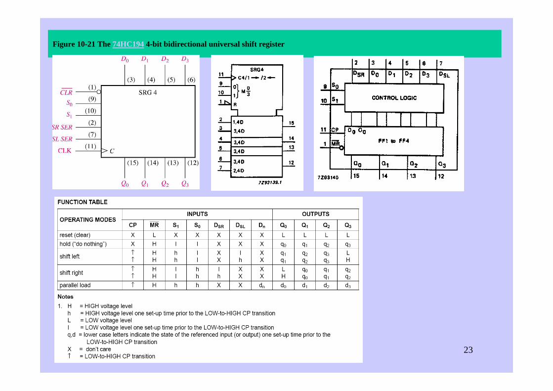
Figure 10-21 The 74HC1944-bit bidirectional universal shift register
23

Figure 10--22 Sample timing diagram for a 74HC194 shift register.
24Thomas L. FloydDigital Fundamentals, 8e
Copyright ©2003 by Pearson Education, Inc.Upper Saddle River, New Jersey 07458
All rights reserved.

Figure 10--23 Four-bit and 5-bit Johnson counters.
25Thomas L. FloydDigital Fundamentals, 8e
Copyright ©2003 by Pearson Education, Inc.Upper Saddle River, New Jersey 07458
All rights reserved.

Figure 10--24Timing sequence for a 4-bit Johnson counter
Figure 10—25 Timing sequence for a 5-bit Johnson counter
26
Figure 10—25 Timing sequence for a 5-bit Johnson counter

Figure 10--26 A 10-bit ring counter. Open file F10-26 to verify operation.
27Thomas L. FloydDigital Fundamentals, 8e
Copyright ©2003 by Pearson Education, Inc.Upper Saddle River, New Jersey 07458
All rights reserved.
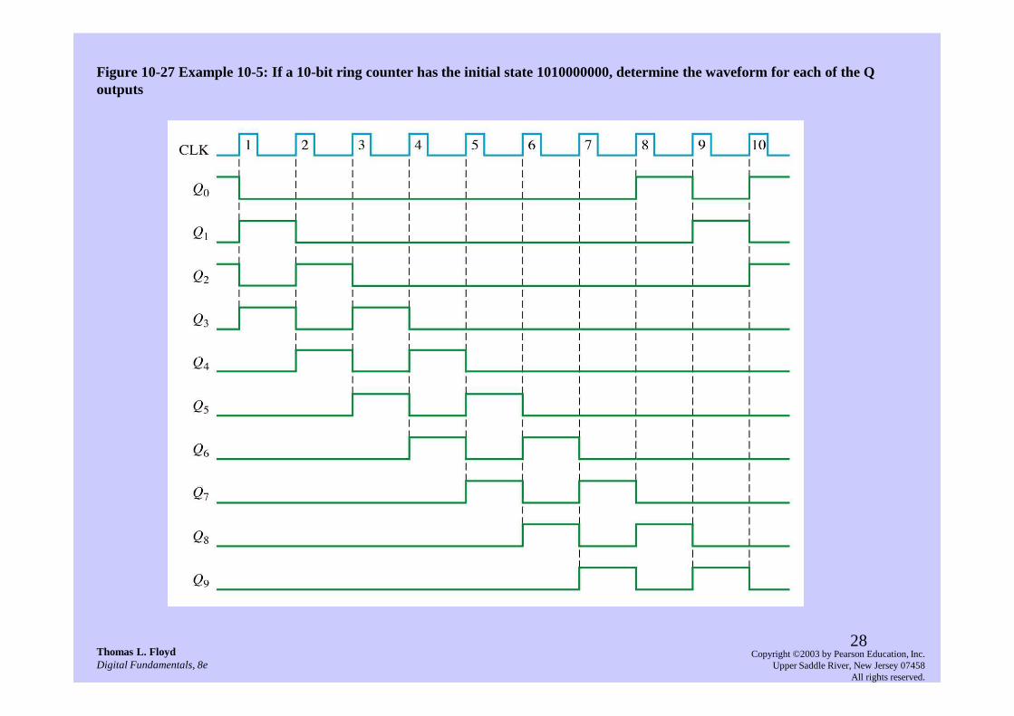
Figure 10-27 Example 10-5: If a 10-bit ring counter has the initial state 1010000000, determine the waveform for each of the Q outputs
28Thomas L. FloydDigital Fundamentals, 8e
Copyright ©2003 by Pearson Education, Inc.Upper Saddle River, New Jersey 07458
All rights reserved.

Figure 10-28The shift register as a time-delay device.
Shift register applications
29Thomas L. FloydDigital Fundamentals, 8e
Copyright ©2003 by Pearson Education, Inc.Upper Saddle River, New Jersey 07458
All rights reserved.

Figure 10-29 Example 10-6: Determine the amount of time delay between the serial input and each output in the next figure.
30Thomas L. FloydDigital Fundamentals, 8e
Copyright ©2003 by Pearson Education, Inc.Upper Saddle River, New Jersey 07458
All rights reserved.

Figure 10--30 Timing diagram showing time delays for the register in Figure 10-29.
31Thomas L. FloydDigital Fundamentals, 8e
Copyright ©2003 by Pearson Education, Inc.Upper Saddle River, New Jersey 07458
All rights reserved.

Figure 10-31 74HC195 connected as a ring counter.
32Thomas L. FloydDigital Fundamentals, 8e
Copyright ©2003 by Pearson Education, Inc.Upper Saddle River, New Jersey 07458
All rights reserved.

Figure 10--33 Simplified logic diagram of a serial-to-parallel converter.
33Thomas L. FloydDigital Fundamentals, 8e
Copyright ©2003 by Pearson Education, Inc.Upper Saddle River, New Jersey 07458
All rights reserved.
Figure 10--34 Serial data format.

Figure 10-35 An example of a timing diagramfor the serial-to-parallel data converterin fig. 10-33.
34Thomas L. FloydDigital Fundamentals, 8e

Figure 10-36UART interface (Universal Asynchronous receiver transmitter)
Figure 10-37 Basic UART blockdiagram
35Thomas L. FloydDigital Fundamentals, 8e
Copyright ©2003 by Pearson Education, Inc.Upper Saddle River, New Jersey 07458
All rights reserved.
diagram
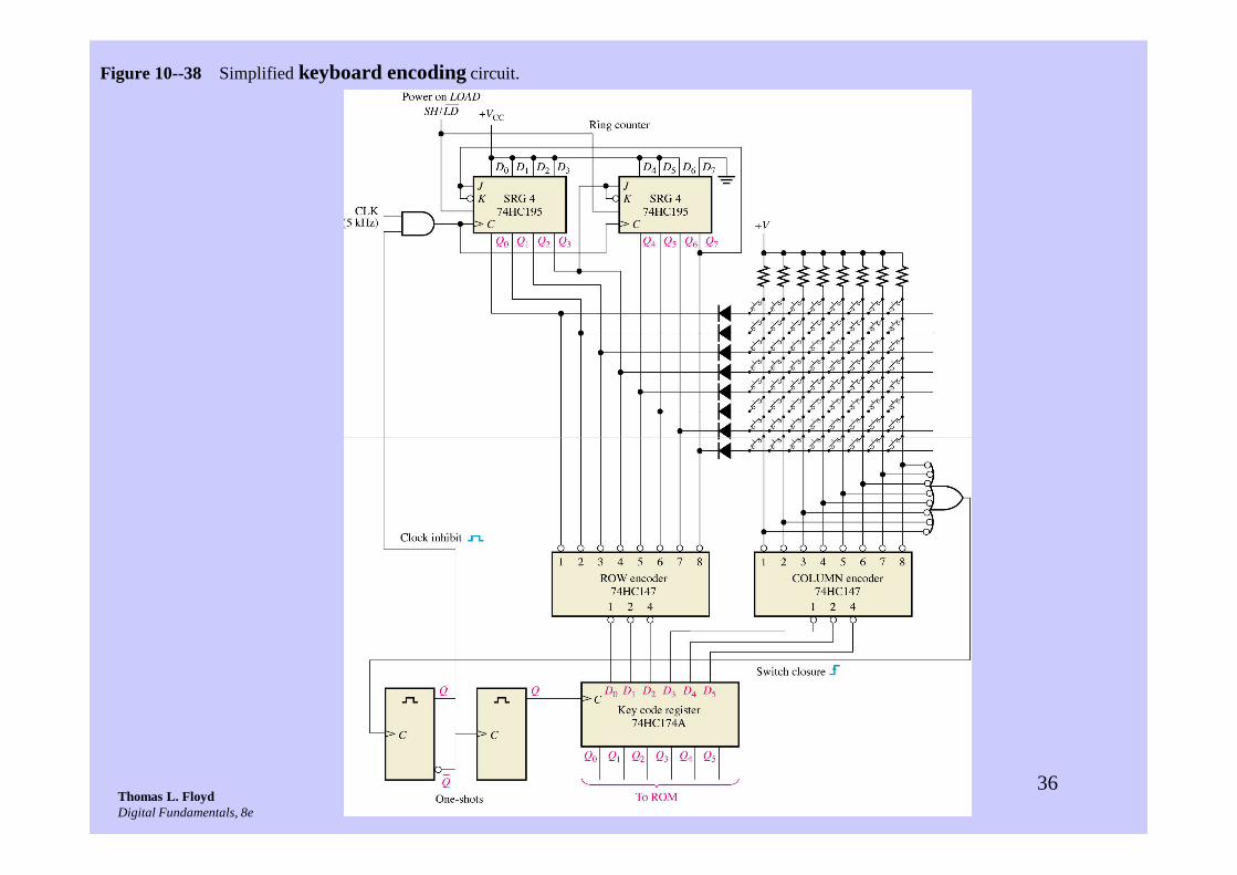
Figure 10--38 Simplified keyboard encodingcircuit.
36Thomas L. FloydDigital Fundamentals, 8e

Figure 10--39 Sample test pattern.
Troubleshooting
37Thomas L. FloydDigital Fundamentals, 8e
Copyright ©2003 by Pearson Education, Inc.Upper Saddle River, New Jersey 07458
All rights reserved.

Figure 10--40 Basic test setup for the serial-to-parallel data converter of Figure 10-33.
38
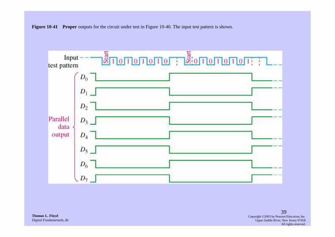
Figure 10-41 Properoutputs for the circuit under test in Figure 10-40. The input test pattern is shown.
39Thomas L. FloydDigital Fundamentals, 8e
Copyright ©2003 by Pearson Education, Inc.Upper Saddle River, New Jersey 07458
All rights reserved.
40

Figure 10-42 Logic symbol for the 74HC164
41Thomas L. FloydDigital Fundamentals, 8e
Copyright ©2003 by Pearson Education, Inc.Upper Saddle River, New Jersey 07458
All rights reserved.
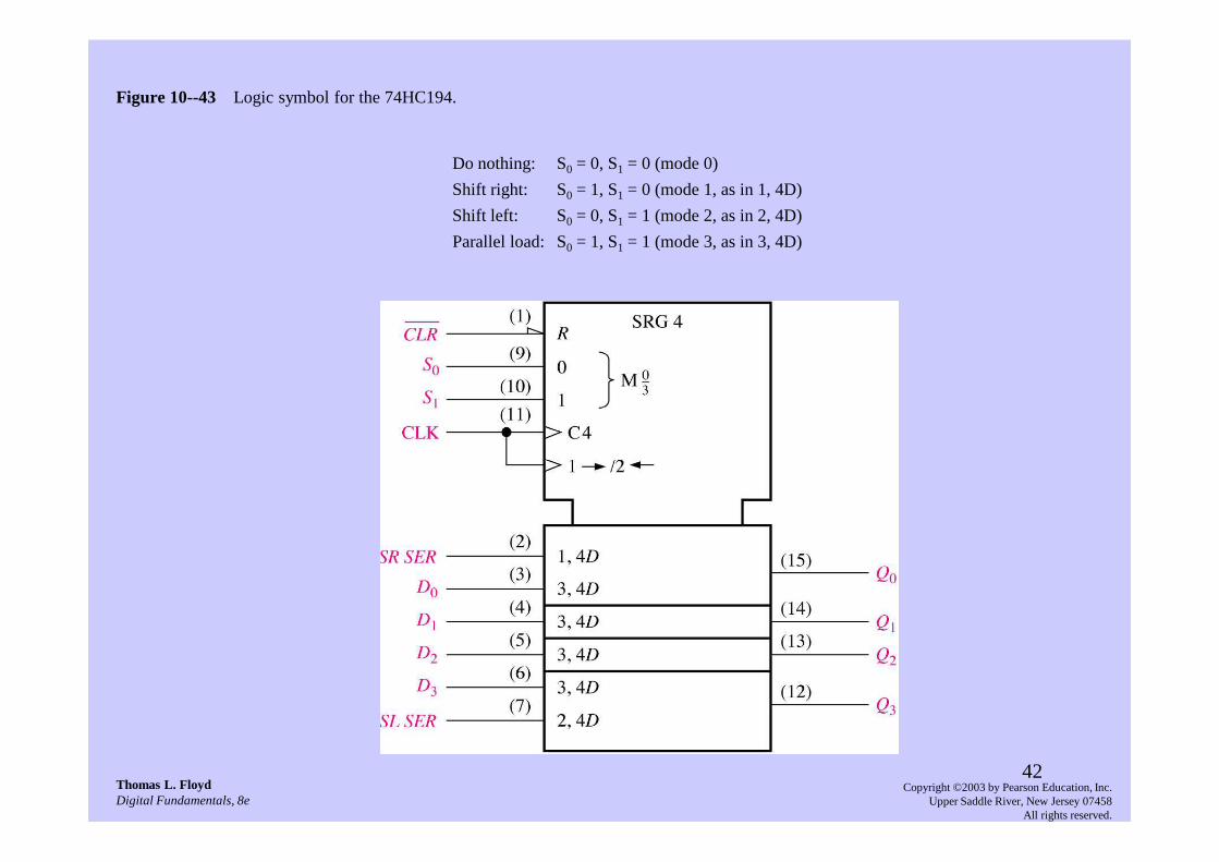
Figure 10--43 Logic symbol for the 74HC194.
Do nothing: S0 = 0, S1 = 0 (mode 0)
Shift right: S0 = 1, S1 = 0 (mode 1, as in 1, 4D)
Shift left: S0 = 0, S1 = 1 (mode 2, as in 2, 4D)
Parallel load: S0 = 1, S1 = 1 (mode 3, as in 3, 4D)
42Thomas L. FloydDigital Fundamentals, 8e
Copyright ©2003 by Pearson Education, Inc.Upper Saddle River, New Jersey 07458
All rights reserved.
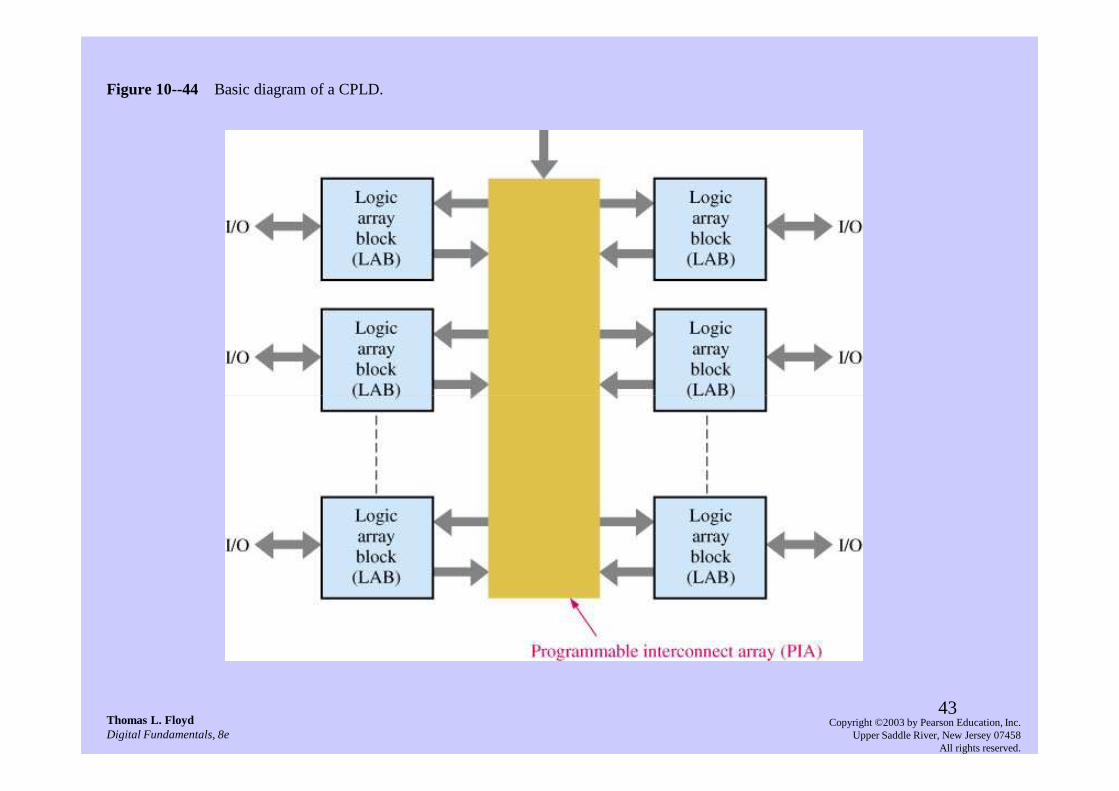
Figure 10--44 Basic diagram of a CPLD.
43Thomas L. FloydDigital Fundamentals, 8e
Copyright ©2003 by Pearson Education, Inc.Upper Saddle River, New Jersey 07458
All rights reserved.
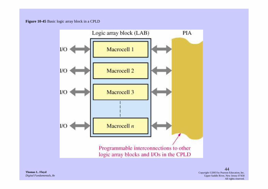
Figure 10-45 Basic logic array block in a CPLD
44Thomas L. FloydDigital Fundamentals, 8e
Copyright ©2003 by Pearson Education, Inc.Upper Saddle River, New Jersey 07458
All rights reserved.
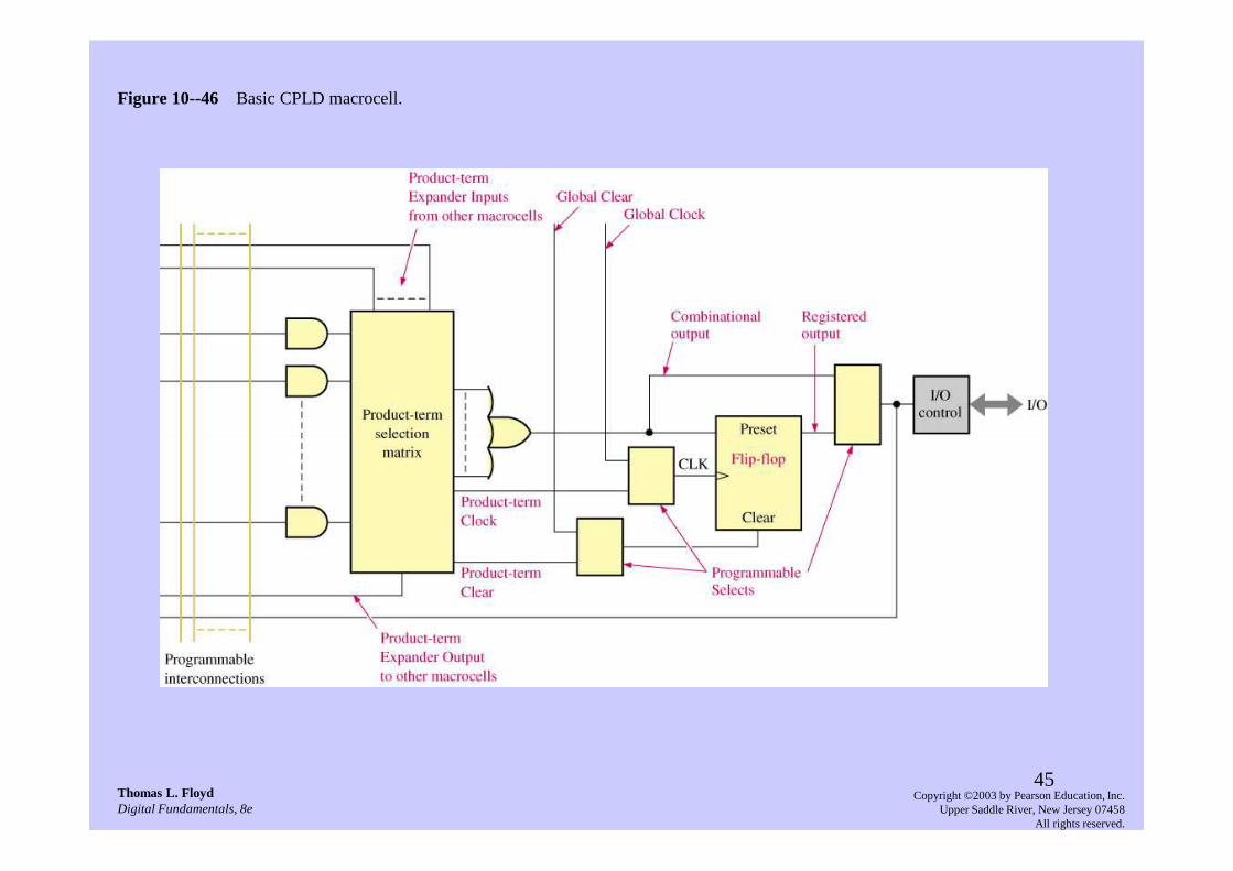
Figure 10--46 Basic CPLD macrocell.
45Thomas L. FloydDigital Fundamentals, 8e
Copyright ©2003 by Pearson Education, Inc.Upper Saddle River, New Jersey 07458
All rights reserved.

Figure 10--47 Basic E2CMOS interconnection technology.
46Thomas L. FloydDigital Fundamentals, 8e
Copyright ©2003 by Pearson Education, Inc.Upper Saddle River, New Jersey 07458
All rights reserved.

Figure 10--48 Block diagram of MAX 7000 CPLDs. Data sheets can be found at www.altera.com.
47Thomas L. FloydDigital Fundamentals, 8e
Copyright ©2003 by Pearson Education, Inc.Upper Saddle River, New Jersey 07458
All rights reserved.

Figure 10--49 Basic logic diagramof the security entry system.
48Thomas L. FloydDigital Fundamentals, 8e

Figure 10--50
49Thomas L. FloydDigital Fundamentals, 8e
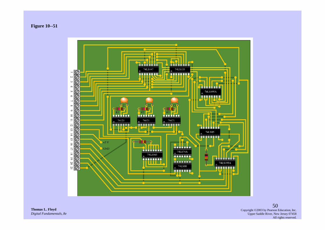
Figure 10--51
50Thomas L. FloydDigital Fundamentals, 8e
Copyright ©2003 by Pearson Education, Inc.Upper Saddle River, New Jersey 07458
All rights reserved.

Figure 10--52
51Thomas L. FloydDigital Fundamentals, 8e
Copyright ©2003 by Pearson Education, Inc.Upper Saddle River, New Jersey 07458
All rights reserved.


