DIGITAL ELECTRONIC CIRCUITS · Example: The bit assignment 1001, can be seen by its weights to...
55
DIGITAL ELECTRONIC CIRCUITS SUBJECT CODE: PEI4I103 B.Tech, Fourth Semester Prepared By Dr. Kanhu Charan Bhuyan Asst. Professor Instrumentation and Electronics Engineering COLLEGE OF ENGINEERING AND TECHNOLOGY BHUBANESWAR
Transcript of DIGITAL ELECTRONIC CIRCUITS · Example: The bit assignment 1001, can be seen by its weights to...

DIGITAL ELECTRONIC CIRCUITS
SUBJECT CODE: PEI4I103
B.Tech, Fourth Semester
Prepared By
Dr. Kanhu Charan Bhuyan
Asst. Professor
Instrumentation and Electronics Engineering
COLLEGE OF ENGINEERING AND TECHNOLOGY
BHUBANESWAR

B.Tech (E&IE/AE&I) detail Syllabus for Admission Batch 2015-16
PEI4I103- DIGITAL ELECTRONICS
University level 80%
MODULE – I (12 Hours)1. Number System: Introduction to various number systems and their
Conversion. Arithmetic Operation using 1’s and 2`s Compliments, Signed Binary and Floating
Point Number Representation Introduction to Binary codes and their applications. (5 Hours)
2. Boolean Algebra and Logic Gates: Boolean algebra and identities, Complete Logic set, logic
gates and truth tables. Universal logic gates, Algebraic Reduction and realization using logic gates
(3 Hours)
3. Combinational Logic Design: Specifying the Problem, Canonical Logic Forms, Extracting
Canonical Forms, EX-OR Equivalence Operations, Logic Array, K-Maps: Two, Three and Four
variable K-maps, NAND and NOR Logic Implementations. (4 Hours)
MODULE – II (14 Hours)
4. Logic Components: Concept of Digital Components, Binary Adders, Subtraction and Multiplication, An Equality Detector and comparator, Line Decoder, encoders, Multiplexers and De-multiplexers. (5 Hours)
5. Synchronous Sequential logic Design: sequential circuits, storage elements: Latches (SR,D),
Storage elements: Flip-Flops inclusion of Master-Slave, characteristics equation and state
diagram of each FFs and Conversion of Flip-Flops. Analysis of Clocked Sequential circuits and
Mealy and Moore Models of Finite State Machines (6 Hours)
6. Binary Counters: Introduction, Principle and design of synchronous and asynchronous
counters, Design of MOD-N counters, Ring counters. Decade counters, State Diagram of binary
counters (4 hours)
MODULE – III (12 hours)
7. Shift resistors: Principle of 4-bit shift resistors. Shifting principle, Timing Diagram, SISO, SIPO, PISO and PIPO resistors. (4 hour)
8. Memory and Programmable Logic: Types of Memories, Memory Decoding, error detection and correction), RAM and ROMs. Programmable Logic Array, Programmable Array Logic, Sequential Programmable Devices. (5 Hours)

9. IC Logic Families: Properties DTL, RTL, TTL, I2L and CMOS and its gate level implementation.
A/D converters and D/A converters (4 Hours)
Text book
1. Digital Design, 3rd Edition, Moris M. Mano, Pearson Education.
2. Fundamentals of digital circuits, 8th edition, A. Anand Kumar, PHI
3. Digital Fundamentals, 5th Edition, T.L. Floyd and R.P. Jain, Pearson Education, New
Delhi.

MODULE – I
NUMBER SYSTEMS Many number systems are in use in digital technology. The most common are the decimal,
binary, octal, and hexadecimal systems. The decimal system is clearly the most familiar to us
because it is a tool that we use every day. Examining some of its characteristics will help us to
better understand the other systems. In the next few pages we shall introduce four numerical
representation systems that are used in the digital system. There are other systems, which we will
look at briefly.
Decimal
Binary
Octal
Hexadecimal
Decimal System The decimal system is composed of 10 numerals or symbols. These 10 symbols are 0, 1, 2, 3, 4, 5, 6, 7, 8,
9. Using these symbols as digits of a number, we can express any quantity. The decimal system is also
called the base-10 system because it has 10 digits.
Decimal Examples 3.1410, 5210 , 102410 , 6400010
Binary System In the binary system, there are only two symbols or possible digit values, 0 and 1. This
base-2 system can be used to represent any quantity that can be represented in decimal or other
base system. In digital systems the information that is being processed is usually presented in
binary form. Binary quantities can be represented by any device that has only two operating states
or possible conditions.
E.g. A switch is only open or closed. We arbitrarily (as we define them) let an open switch
represent binary 0 and a closed switch represent binary 1. Thus we can represent any binary
number by using series of switches.
Octal System The octal number system has a base of eight, meaning that it has eight possible
digits:0,1,2,3,4,5,6,7.
Octal to Decimal Conversion
2378 = 2 x (82) + 3 x (81) + 7 x (80) = 15910

24.68 = 2 x (81) + 4 x (80) + 6 x (8-1) = 20.7510
11.18 = 1 x (81) + 1 x (80) + 1 x (8-1) = 9.12510
12.38 = 1 x (81) + 2 x (80) + 3 x (8-1) = 10.37510
Hexadecimal System The hexadecimal system uses base 16. Thus, it has 16 possible digit symbols. It uses the
digits 0 through 9 plus the letters A, B, C, D, E, and F as the 16 digit symbols.
Hexadecimal to Decimal Conversion
24.616 = 2 x (161) + 4 x (160) + 6 x (16-1) = 36.37510
11.116 = 1 x (161) + 1 x (160) + 1 x (16-1) = 17.062510
12.316 = 1 x (161) + 2 x (160) + 3 x (16-1) = 18.187510
Code Conversion Converting from one code form to another code form is called code conversion, like converting
from binary to decimal or converting from hexadecimal to decimal.
Binary-To-Decimal Conversion
Any binary number can be converted to its decimal equivalent simply by summing together the
weights of the various positions in the binary number which contain a 1.e.g.
110112=24+23+01+21+20=16+8+0+2+1=2710
Octal-To-Binary Conversion
Each Octal digit is represented by three binary digits.
Example: 4 7 28= (100) (111) (010)2 = 100 111 0102
Octal-To-Hexadecimal Hexadecimal-To-Octal Conversion
Convert Octal (Hexadecimal) to Binary first.
Regroup the binary number by three bits per group starting from LSB if Octal is required.
Regroup the binary number by four bits per group starting from LSB if Hexadecimal is
required.
Arithmetic Operation using 1’s and 2’s Complement
1’s Complement
The 1’s complement of a binary number is defined as the value obtained by inverting all
the bits in the binary representation of the number (swapping 0’s for 1’s and vice versa). The 1’s
complement of the number then behaves like the negative of the original number in some
arithmetic operations.

Example: 1’s complement of 10111 is 01000.
2’s Complement
To get 2’s complement of a binary number we add one (1) to the 1’s complement of that
same binary number.
Example: 2’s complement of 10111 is; 1’s complement of 10111 + 1
=> 01000 + 1 = 01001
Arithmetic Operation
1. Using 1’s complement:
Example1: Subtract 134 from 168.
168-134 = 168 + (-134)
Binary representation of 168= 1010 1000
Binary representation of 134= 1000 0110
Binary representation of -134= 0111 1001
[Because 1’s complement represents the negative magnitude of a binary number]
168 + (-134)= 1010 1000
+ 0111 1001
10010 0001
As a carry bit is present, 1 will be added to the result and it represents that the result is
positive.
0010 0001 + 1 = 0010 0010
Decimal representation of 0010 0010 is 34.
168-134=34; hence the result is correct.
Example2: Subtract 168 from 134.
134-168 = 134 + (-168)
Binary representation of 134= 1000 0110
Binary representation of 168= 1010 1000
Binary representation of -168= 0101 0111
[Because 1’s complement represents the negative magnitude of a binary number]

134 + (-168)= 1000 0110
+ 0101 0111
1101 1101
As a carry bit is absent, 1’s complement of this value will be the final result and absence
of carry bit represents that the result is negative.
1’s complement of 1101 1101 = 0010 0010
Decimal representation of 0010 0010 is 34. As carry bit is absent the result is negative i.e -34
134 -168= -34; hence the result is correct.
2. Using 2’s complement:
Example 1: Subtract 96 from 118.
118-96 = 118 + (-96)
Binary representation of 118= 0111 0110
Binary representation of 96= 0110 0000
Here 2’s complement represents the negative magnitude of a binary number.
Hence 2’s complement of 96 represents -96.
So -96= 1001 1111
118 + (-96) = 0111 0110
+ 1001 1111
10001 0101
As a carry bit is present, 1 will be added to the result and presents of carry bit represents
that the result is positive.
0001 0101+ 1= 0001 0110
Decimal representation of 0001 0110 is 22. As carry bit is present the result is positive.
Example 2: Subtract 118 from 96.
118-96 = 96 + (-118)
Binary representation of 96= 0110 0000
Binary representation of 118= 0111 0110
Here 2’s complement represents the negative magnitude of a binary number.
Hence 2’s complement of 118 represents -118.

So -118= 1000 1010
96 + (-118) = 0110 0000
+ 1000 1010
1110 1010
As a carry bit is absent, 2’s complement of this value will be the final result and absence
of carry bit represents that the result is negative.
2’s complement of 1110 1010 = 0001 0110
Decimal representation of 0001 0110 is 34. As carry bit is absent the result is negative i.e -34.
Binary Codes Binary codes are codes which are represented in binary system with modification from the original
ones. Below we will be seeing the following:
Weighted Binary Systems
Non Weighted Codes
Weighted Binary Systems Weighted binary codes are those which obey the positional weighting principles, each position of
the number represents a specific weight. The binary counting sequence is an example.
8421 Code/BCD Code
The BCD (Binary Coded Decimal) is a straight assignment of the binary equivalent. It is possible
to assign weights to the binary bits according to their positions. The weights in the
BCD code are 8,4,2,1.
Example: The bit assignment 1001, can be seen by its weights to represent the decimal 9 because:
1x8+0x4+0x2+1x1 = 9
2421 Code
This is a weighted code, its weights are 2, 4, 2 and 1. A decimal number is represented in 4- bit
form and the total four bits weight is 2 + 4 + 2 + 1 = 9. Hence the 2421 code represents the decimal
numbers from 0 to 9.
5211 Code
This is a weighted code, its weights are 5, 2, 1 and 1. A decimal number is represented in 4- bit
form and the total four bits weight is 5 + 2 + 1 + 1 = 9. Hence the 5211 code represents the decimal
numbers from 0 to 9.

Reflective Code A code is said to be reflective when code for 9 is complement for the code for 0, and so is for 8
and 1 codes, 7 and 2, 6 and 3, 5 and 4. Codes 2421, 5211, and excess-3 are reflective, whereas the
8421 code is not.
Excess-3 Code Excess-3 is a non-weighted code used to express decimal numbers. The code derives its name from
the fact that each binary code is the corresponding 8421 code plus 0011(3).
Example: representation of 7 in Excess-3 code is :-
BCD code of 7 = 0111
Excess-3 code of 7 = BCD + 0011 = 1010
Gray Code The gray code belongs to a class of codes called minimum change codes, in which only one bit in
the code changes when moving from one code to the next. The Gray code is non weighted code,
as the position of bit does not contain any weight. The gray code is are reflective digital code which
has the special property that any two subsequent numbers codes differ by only one bit. This is also
called a unit-distance code. In digital Gray code has got a special place.
Example: Write the Gray code of 7.
Step-1 BCD code of 7 = 0111
Step-2 Keep the MSB of BCD same and then add it with the next digit. Ignore the carry bit in each
case.
(0111)2 = (0100)G
0 1 1 1 = 0100
Error Detecting and Correction Codes For reliable transmission and storage of digital data, error detection and correction is required.
Below are a few examples of codes which permit error detection and error correction after
detection.
Error Detecting Codes
When data is transmitted from one point to another, like in wireless transmission, or it is just stored,
like in hard disks and memories, there are chances that data may get corrupted. To detect these
data errors, we use special codes, which are error detection codes.
Parity
In parity codes, every data byte, or nibble (according to how user wants to use it) is checked if
they have even number of ones or even number of zeros. Based on this information an additional
bit is appended to the original data. Thus if we consider 8-bit data, adding the parity bit will make
it 9 bit long.
+ + +

At the receiver side, once again parity is calculated and matched with the received parity (bit 9),
and if they match, data is ok, otherwise data is corrupt.
There are two types of parity:
Even parity: Checks if there is an even number of ones; if so, parity bit is zero. When the
number of ones is odd then parity bit is set to 1.
Odd Parity: Checks if there is an odd number of ones; if so, parity bit is zero. When number
of ones is even then parity bit is set to 1.
Error-Correcting Codes
Error correcting codes not only detect errors, but also correct them. This is used normally in
Satellite communication, where turn-around delay is very high as is the probability of data getting
corrupt.
ECC (Error correcting codes) are used also in memories, networking, Hard disk, CDROM,
DVD etc. Normally in networking chips (ASIC), we have 2 Error detection bits and 1 Error
correction bit.
Hamming Code Hamming code adds a minimum number of bits to the data transmitted in a noisy channel, to be
able to correct every possible one-bit error. It can detect (not correct) two bits errors and cannot
distinguish between 1-bit and 2-bits inconsistencies. It can't – in general – detect 3(or more)-bits
errors The idea is that the failed bit position in an n-bit string (which we'll call X) can be
represented in binary with log2 (n) bits, hence we'll try to get it adding just log2(n) bits.
ASCII Code ASCII stands for American Standard Code for Information Interchange. It has become a world
standard alphanumeric code for microcomputers and computers. It is a 7-bit code representing 27
= 128 different characters. These characters represent 26 upper case letters
(A to Z), 26 lowercase letters (a to z), 10 numbers (0 to 9), 33 special characters and symbols and
33 control characters.
Boolean algebra and Logic Gates The English mathematician George Boole (1815-1864) sought to give symbolic form to Aristotle’s
system of logic. Boole wrote a treatise on the subject in 1854, titled an Investigation of the Laws
of Thought, on Which Are Founded the Mathematical Theories of Logic and Probabilities, which
codified several rules of relationship between Mathematical quantities limited to one of two
possible values: true or false, 1 or 0. His Mathematical system became known as Boolean algebra.
All arithmetic operations performed with Boolean quantities have but one of two possible
Outcomes: either 1 or 0. There is no such thing as ‖2‖ or ‖-1‖ or ‖1/2‖ in the Boolean
world.

It is a world in which all other possibilities are invalid by fiat. As one might guess, this is not the
kind of math you want to use when balancing a check book or calculating current through a resistor.
However, Claude Shannon of MIT fame recognized how Boolean algebra could be applied to on-
and-off circuits, where all signals are characterized as either ‖high‖ (1) or ‖low‖ (0). His1938
thesis, titled A Symbolic Analysis of Relay and Switching Circuits, put Boole’s theoretical work
to use in a way Boole never could have imagined, giving us a Powerful mathematical tool for
designing and analysing digital circuits.
Like ‖normal‖ algebra, Boolean algebra uses alphabetical letters to denote variables.
Unlike ‖normal‖ algebra, though, Boolean variables are always CAPITAL letters, never
lowercase.
Boolean Arithmetic Let us begin our exploration of Boolean algebra by adding numbers together:
0 + 0 = 0
0 + 1 = 1
1 + 0 = 1
1 + 1 = 1
The first three sums make perfect sense to anyone familiar with elementary addition.
The Last sum, though, is quite possibly responsible for more confusion than any other
Single statement in digital electronics, because it seems to run contrary to the basic principles of
mathematics. Well, it does contradict principles of addition for real numbers, but not for Boolean
numbers. Remember that in the world of Boolean algebra, there are only two possible values for
any quantity and for any arithmetic operation: 1 or 0. There is no such thing as ‖2‖ within the
scope of Boolean values. Since the sum ‖1 + 1‖ certainly isn’t 0, it must be 1 by process of
elimination.
Principle of Duality
It states that every algebraic expression is deducible from the postulates of Boolean algebra and it
remains valid if the operators & identity elements are interchanged. If the inputs of a NOR gate
are inverted, we get a AND equivalent circuit. Similarly, when the inputs of a NAND gate are
inverted, we get an OR equivalent circuit. This property is called duality.
Theorems of Boolean algebra and Identities The theorems of Boolean algebra can be used to simplify many a complex Boolean expression and
also to transform the given expression into a more useful and meaningful equivalent expression.
The theorems are presented as pairs, with the two theorems in a given pair being the dual of each
other. These theorems can be very easily verified by the method of ‘perfect induction’. According
to this method, the validity of the expression is tested for all possible combinations of values of

the variables involved. Also, since the validity of the theorem is based on its being true for all
possible combinations of values of variables, there is no reason why a variable cannot be replaced
with its complement, or vice versa, without disturbing the validity. Another important point is that,
if a given expression is valid, its dual will also be valid.
Theorem 1 (Operations with ‘0’ and ‘1’)
(a) 0.X = 0 and (b) 1+X= 1
Where X is not necessarily a single variable – it could be a term or even a large expression.
Theorem 1(a) can be proved by substituting all possible values of X, that is, 0 and 1, into
the given expression and checking whether the LHS equals the RHS:
• For X = 0, LHS = 0.X = 0.0 = 0 = RHS.
• For X= 1, LHS = 0.1 = 0 = RHS.
Thus, 0.X =0 irrespective of the value of X, and hence the proof.
Theorem 1(b) can be proved in a similar manner. In general, according to theorem 1, 0. (Boolean
expression) = 0 and 1+ (Boolean expression) =1.
1. For example: 0. (A.B + B.C +C.D) = 0 and 1+ (A.B+B.C +C.D) = 1, where A, B and C are
Boolean variables.
Theorem 2 (Operations with ‘0’ and ‘1’)
(a) 1.X = X and (b) 0+X = X
where X could be a variable, a term or even a large expression.
According to this theorem, ANDing a Boolean expression to ‘1’ or ORing ‘0’ to it makes no
difference to the expression:
For X = 0, LHS = 1.0 = 0 = RHS.
For X = 1, LHS = 1.1 = 1 = RHS.
Also,
1. (Boolean expression) = Boolean expression and 0 + (Boolean expression) = Boolean expression.
For example,
1.(A+B.C + C.D) = 0+(A+B.C +C.D) = A+B.C +C.D
Theorem 3 (Idempotent or Identity Laws)
(a) X.X.X……X = X and (b) X+X+X +···+X = X
Theorems 3(a) and (b) are known by the name of idempotent laws, also known as identity laws.

Theorem 3(a) is a direct outcome of an AND gate operation, whereas theorem 3(b) represents an
OR gate operation when all the inputs of the gate have been tied together. The scope of idempotent
laws can be expanded further by considering X to be a term or an expression. For example, let us
apply idempotent laws to simplify the following Boolean expression:
Theorem 4 (Complementation Law)
(a) X_X = 0 and (b) X+X = 1
According to this theorem, in general, any Boolean expression when ANDed to its complement
yields a ‘0’ and when ORed to its complement yields a ‘1’, irrespective of the
complexity of the expression:
Hence, theorem 4(a) is proved. Since theorem 4(b) is the dual of theorem 4(a), its proof is implied.
The example below further illustrates the application of complementation laws:
Theorem 5 (Commutative property)
Mathematical identity, called a ‖property‖ or a ‖law‖ describes how differing variables relate
to each other in a system of numbers. One of these properties is known as the commutative
property, and it applies equally to addition and multiplication.
In essence, the commutative property tells us we can reverse the order of variables that are either
added together or multiplied together without changing the truth of the expression:
Commutative property of addition
A + B = B + A
Commutative property of multiplication
AB = BA
Theorem 6 (Associative Property)
The Associative Property, again applying equally well to addition and multiplication.
This property tells us we can associate groups of added or multiplied variables together with
parentheses without altering the truth of the equations.

Associative property of addition
A + (B + C) = (A + B) + C
Associative property of multiplication
A (BC) = (AB) C
Theorem 7 (Distributive Property)
The Distributive Property, illustrating how to expand a Boolean expression formed by the product
of a sum, and in reverse shows us how terms may be factored out of Boolean sums-of-products:
Distributive property
A (B + C) = AB + AC
Theorem 8 (Absorption Law or Redundancy Law)
(a) X+X.Y = X and (b) X.(X+Y) = X
The proof of absorption law is straightforward:
X+X.Y = X. (1+Y) = X.1 = X
Theorem 8(b) is the dual of theorem 8(a) and hence stands proved.
The crux of this simplification theorem is that, if a smaller term appears in a larger term, then the
larger term is redundant. The following examples further illustrate the underlying concept:
De-Morgan’s First Theorem
It States that the complement of the sum of the variables is equal to the product of the complement
of each variable. This theorem may be expressed by the following Boolean expression.
BABA .
De-Morgan’s Second Theorem
It states that the complement of the product of variables is equal to the sum of Complements of
each individual variables‖. Boolean expression for this theorem is
BABA .

Boolean Function Boolean functions are represented in various forms. The two popular forms are truth tables and
Venn diagram. Truth tables represent functions in a tabular form, while Venn diagram provide a
graphic representation. In addition, there are two algebraic representation known as the standard
form or canonical form.
Example: Truth table for Z= AB’ + A’C + A’B’C
There are three variables present in the equation; A, B, C. Hence, there will be 23 = 8
combinations of values. These eight combinations are shown in the first three columns of the truth
table. These combinations corresponds to binary numbers 000 through 111.
To evaluate Z in the example function, knowing the values for A,B,C at each row of the
truth table, we should first generate the values for A’ and B’ and then generate the values of AB’,
A’C and A’B’C by ANDing the values in the appropriate columns for each row. Finally, we should
derive the values of Z by ORing the values in the last three columns for each row. Note that
evaluating A’B’C corresponds to ANDing A’ and B’ values, followed by ANDing the value of C.
Complete Logic Sets
The basic logic gates are NOT, AND and OR. The complex logic functions like NAND, NOR,
XOR, XNOR are crested by using these basic logic gates. The last two are not standard terms; they
stand for ‘inverter’ and ‘buffer’, respectively. The symbols for these gates and their corresponding
Boolean expressions are given in Fig. 2.

All of the logical gate functions, as well as the Boolean relations discussed in the next section,
follow from the truth tables for the AND and OR gates. A complete set of logic operations is one
that allows us to create every possible logic function using only those in the set.
Basic Logic Operations Boolean algebra is based on a set of logic operations that define basic functions. They are
performed using one or more input variables and they result in a single output bit.
NOT Operation
Because they are allowed to possess only one of two possible values, either 1 or 0, each and every
variable has a complement: the opposite of its value. For example, if variable ‖A‖ has a value
of 0, then the complement of A has a value of 1. Boolean notation uses a bar above the variable
character to denote complementation, like this:
If: A=0, then: Ā=1
If: A=1,then: Ā=0
In written form, the complement of ‖A‖ denoted as ‖A-not‖ or ‖A-bar‖. Sometimes a
‖prime‖symbol is used to represent complementation. For example, A‘would be the
complement of A, much the same as using a prime symbol to denote differentiation in calculus

rather than the fractional notation dot. Usually, though, the ‖bar‖ symbol finds more wide spread
use than the ‖prime‖ symbol, for reasons that will become more apparent later in this chapter.
Truth Table:
A Ā
0 1
1 0
Symbol:
OR Operation
Let us consider there are two input bits, A and B. each of two bits can assume a value of 0 or 1. So
22=4 possible combinations can occur. This can be listed as AB= 00, 01, 10, 11.
A OR B can be restated as A + B. We usually employ the symbol “+” to denote OR operation.
A OR B = A + B
Example: If A=1, B=1 then,
A OR B = A + B = 1
Truth Table:
Symbol
AND Operation
This operation detects the situation where all of the inputs are equal to 1 for this case. For two
inputs A and B, we define the AND logic by writing
A AND B = A.B
If both A=1 and B=1,
then
A AND B = 1
else
A B A + B
0 0 0
0 1 1
1 0 1
1 1 1
A Ā
A
B A+B

A AND B = 0
Truth Table:
A B A.B
0 0 0
0 1 0
1 0 0
1 1 1
Symbol
Universal Logic Gates
NAND Logic Gate
The name NAND is the shorten form of NOT-AND and means the output is defined as the
complement of the AND gate. With the inputs A and B, the NAND operation is denoted as BA. .
This is equivalent to the statement
If either input is 0,
then
BA. =1
else
BA. =0
Truth Table:
A B BA.
0 0 1
0 1 1
1 0 1
1 1 0
Symbol:
NOR Logic Gate
The name NOR is the shorten form of NOT-OR and means the output is defined as the complement
of the OR gate. With the inputs A and B, the NOR operation is denoted as BA . This is equivalent
to the statement
If either input is 0,
then
BA =1
A
B A.B
A
B
BA.

else
BA =0
Truth Table:
A B BA 0 0 1
0 1 0
1 0 0
1 1 0
Symbol:
Algebraic Reduction One common problem in combinational logic design is reduction of a logic expression to
the “simplest” possible form; “simplest” usually means that we want to implement the function
using the smallest no of gates. The reduction is accomplished by applying the basic identities in a
step-by-step manner. Some basic rules are summarized in table given below to aid in the task.
OR Identities AND Identities
A+0=A A.0=0
A+1=1 A.1=A
A+A=A A.A=A
A+Ā=1 A.Ā=0
AA -
A+B=B+A A.B=B.A
A+(B+C)=(A+B)+C A.(B.C)=(A.B).C
A.(B+C)=A.B+A.C A+(B.C)=(A+B).(A+C)
BABA .)( BABA ).(
A+A.B=A BABAA .
Combinational Logic Design
Specifying the problem Combinational logic deals with networks that use logic gates to combine the input variables as
needed to produce logic functions. In combinational circuits the value of the input depends on the
current values of the inputs. To design a combinational logic network, we usually start with a
specified set of inputs to produce output.

Canonical form of Boolean Expression
Product-of-Sums Expressions
A product-of-sums expression contains the product of different terms, with each term being either
a single literal or a sum of more than one literal. It can be obtained from the truth table by
considering those input combinations that produce a logic ‘0’ at the output. Each such input
combination gives a term, and the product of all such terms gives the expression.
Different terms are obtained by taking the sum of the corresponding literals. Here‘0’ and ‘1’
respectively mean the un-complemented and complemented variables, unlike sum-of products
expressions where ‘0’ and ‘1’ respectively mean complemented and un-complemented variables.
Since each term in the case of the product-of-sums expression is going to be the sum of literals,
this implies that it is going to be implemented using an OR operation. Now, an OR gate produces
a logic ‘0’only when all its inputs are in the logic ‘0’state, which means that the first term
corresponding to the second row of the truth table will be A+B+C. The product-of-sums Boolean
expression for this truth table is given by transforming the given product-of-sums expression into
an equivalent sum-of-products expression is a straight forward process. Multiplying out the given
expression and carrying out the obvious simplification provides the equivalent sum-of-products
expression:
)).((),( yxyxyxF
Sum of Products expression
A given sum-of-products expression can be transformed into an equivalent product-of sums
expression by (a) taking the dual of the given expression, (b) multiplying out different terms to get
the sum-of products form, (c) removing redundancy and (d) taking a dual to get the equivalent
product-of-sums expression. As an illustration, let us find the equivalent product of sums
expression of the sum-of products expression

Extracting Canonical Forms Let us investigate this relationship by means of a specific case where we start with the function
table shown below. The input variables are A, B, C and the output function is f(A, B, C).
A B C f
0 0 0 0
0 0 1 1
0 1 0 1
0 1 1 0
1 0 0 1
1 0 1 0
1 1 0 0
1 1 1 1
From the table output f can be represented as
f= f1+f2+f3+f4
where,
f1= CBA
f2= CBA
f3= CBA
f4= ABC
Hence the complete expression will be
f= CBA + CBA + CBA + ABC
Minterms and Maxterms
A minterm is the product of N distinct literals where each literal occurs exactly any Boolean
expression may be expressed in terms of either minterms or maxterms. To do this we must first
define the concept of a literal. A literal is a single variable within a term which may or may not be
complemented. For an expression with N variables, minterms and maxterms are defined as follows
once.
A maxterm is the sum of N distinct literals where each literal occurs exactly once.

The Exclusive-OR and Equivalence Operation By definition, the X-OR gate provides an output that is identical to that of the OR gate
except for the case where both inputs are 1; the XOR output is 0 in this case. The name “exclusive-
OR” arises from this exception in that the output is a 1 when only a single input is 1 exclusively,
that is, by itself.
A B BA
0 0 0
0 1 1
1 0 1
1 1 0
Symbol:
The logical description of the gate can be extracted from the function table. The two cases that
results in a 1 at the output are AB=01 and AB=10, so the function is given by
BABABA ..
The complement of the XOR function is the exclusive NOR (XNOR) operation; which can be
denoted as BA . The function is given by
BABABA ..
By reading off the SOP terms where the output is 1, this shows that it is only possible when bot
the inputs are same; i.e A=B. Because of this property, the XNOR is also referredto as the
“equivalence function”.
Function Table:
A B BA
0 0 1
0 1 0
1 0 0
1 1 1
Symbol:

Karnaugh Map Maurice Karnaugh, a telecommunications engineer, developed the Karnaugh map at Bell Labs in
1953 while designing digital logic based telephone switching circuits. Karnaugh maps reduce logic
functions more quickly and easily compared to Boolean algebra. By reduce we mean simplify,
reducing the number of gates and inputs. We like to simplify logic to a lowest cost form to save
costs by elimination of components. We define lowest cost as being the lowest number of gates
with the lowest number of inputs per gate. A Karnaugh map is a graphical representation of the
logic system. It can be drawn directly from either minterm (sum-of-products) or maxterm (product-
of-sums) Boolean expressions. Drawing a Karnaugh map from the truth table involves an
additional step of writing the minterm or maxterm expression depending upon whether it is desired
to have a minimized sum-of products or a minimized product of-sums expression.
Construction of a Karnaugh Map
An n-variable Karnaugh map has 2n squares, and each possible input is allotted a square. In the
case of a minterm Karnaugh map, ‘1’ is placed in all those squares for which the output is ‘1’ and
‘0’ is placed in all those squares for which the output is ‘0’. 0s are omitted for simplicity. An ‘X‘
is placed in squares corresponding to ‘don‘t care conditions. In the case of a maxterms Karnaugh
map, a ‘1’ is placed in all those squares for which the output is ‘0’, and a ‘0’ is placed for input
entries corresponding to a ‘1’ output. Again, 0s are omitted for simplicity, and an ‘X‘ is placed in
squares corresponding to ‘don’t care’ conditions. The choice of terms identifying different rows
and columns of a Karnaugh map is not unique for a given number of variables. The only condition
to be satisfied is that the designation of adjacent rows and adjacent columns should be the same
except for one of the literals being complemented. Also, the extreme rows and extreme columns
are consider adjacent. Some of the possible designation styles for two, three and four variable
minterm Karnaugh maps are shown in the figure below.
The style of row identification need not be the same as that of column identification as long as it
meets the basic requirement with respect to adjacent terms. It is, however, accepted practice to
adopt a uniform style of row and column identification. Also, the style shown in the figure below
is more commonly used. A similar discussion applies for maxterms Karnaugh maps. Having drawn
the Karnaugh map, the next step is to form groups of 1s as per the following guidelines:
Each square containing a ‘1’ must be considered at least once, although it can be considered
as often as desired.

The objective should be to account for all the marked squares in the minimum number of
groups.
The number of squares in a group must always be a power of 2, i.e. groups can have 1, 2,
4, 8, 16, squares.
Each group should be as large as possible, which means that a square should not be
accounted for by itself if it can be accounted for by a group of two squares; a group of two
squares should not be made if the involved squares can be included in a group of four
squares and so on.
‘Don’t care‘entries can be used in accounting for all of 1-squares to make optimum groups.
They are marked ‘X’ in the corresponding squares. It is, however, not necessary to account
for all ‘don’t care’ entries. Only such entries that can be used to advantage should be used.
Two Variable K-Map
Three Variable K-Map

Four Variable K-Map

MODULE – II
Concept of logic components Modern digital networks can be quite complicated, consisting of millions of logic gates. To design
large system, we use the hierarchical approach where the network is broken down into smaller
logic components that perform useful functions. The components themselves may be classified as
basic components for system building even though they consist of smaller components or basic
logic gates.
Binary Adder
Half-Adder A half-adder is an arithmetic circuit block that can be used to add two bits. Such a circuit thus has
two inputs that represent the two bits to be added and two outputs, with one producing the SUM
output and the other producing the CARRY. Figure shows the truth table of a half-adder, showing
all possible input combinations and the corresponding outputs. The Boolean expressions for the
SUM and CARRY outputs are given by the equations below
An examination of the two expressions tells that there is no scope for further simplification. While
the first one representing the SUM output is that of an EX-OR gate, the second one representing
the CARRY output is that of an AND gate. However, these two expressions can certainly be
represented in different forms using various laws and theorems of Boolean algebra to illustrate the

flexibility that the designer has in hardware implementing as simple a combinational function as
that of a half-adder.
Although the simplest way to hardware-implement a half-adder would be to use a two input EX-
OR gate for the SUM output and a two-input AND gate for the CARRY output, as shown in Fig.
it could also be implemented by using an appropriate arrangement of either NAND or NOR gates.
Full Adder A full adder circuit is an arithmetic circuit block that can be used to add three bits to produce a
SUM and a CARRY output. Such a building block becomes a necessity when it comes to adding
binary numbers with a large number of bits. The full adder circuit overcomes the limitation of the
half-adder, which can be used to add two bits only. Let us recall the procedure for adding larger
binary numbers. We begin with the addition of LSBs of the two numbers. We record the sum under
the LSB column and take the carry, if any, forward to the next higher column bits. As a result,
when we add the next adjacent higher column bits, we would be required to add three bits if there
were a carry from the previous addition. We have a similar situation for the other higher column
bits. Also until we reach the MSB. A full adder is therefore essential for the hardware
implementation of an adder circuit capable of adding larger binary numbers. A half-adder can be
used for addition of LSBs only.

Figure shows the truth table of a full adder circuit showing all possible input combinations and
corresponding outputs. In order to arrive at the logic circuit for hardware implementation of a full
adder, we will firstly write the Boolean expressions for the two output variables, that is, the SUM
and CARRY outputs, in terms of input variables. These expressions are then simplified by using
any of the simplification techniques described in the previous chapter. The Boolean expressions
for the two output variables are given in Equation below for the SUM output (S) and in above
Equation for the CARRY output (Cout):
Boolean expression above can be implemented with a two-input EX-OR gate provided that one of
the inputs is Cin and the other input is the output of another two-input EX-OR gate with A and B
as its inputs. Similarly, Boolean expression above can be implemented by ORing two minterms.
One of them is the AND output of A and B. The other is also the output of an AND gate whose
inputs are Cin and the output of an EX-OR operation on A and B. The whole idea of writing the
Boolean expressions in this modified form was to demonstrate the use of a half-adder circuit in
building a full adder. Figure shows logic implementation of Equations above.
Subtractor and Multiplier
Half-Subtractor
We will study the use of adder circuits for subtraction operations in the following pages. Before
we do that, we will briefly look at the counterparts of half-adder and full adder circuits in the half-
subtractor and full subtractor for direct implementation of subtraction operations using logic gates.

A half-subtractor is a combinational circuit that can be used to subtract one binary digit from
another to produce a DIFFERENCE output and a BORROW output. The BORROW output here
specifies whether a ‘1’ has been borrowed to perform the subtraction. The truth table of a half-
subtractor, as shown in Fig. explains this further. The Boolean expressions for the two outputs are
given by the equations
Full-Subtractor
A full subtractor performs subtraction operation on two bits, a minuend and a subtrahend, and also
takes into consideration whether a ‘1‘ has already been borrowed by the previous adjacent lower
minuend bit or not. As a result, there are three bits to be handled at the input of a full subtractor,
namely the two bits to be subtracted and a borrow bit designated as Bin .There are two outputs,
namely the DIFFERENCE output D and the BORROW output Bo. The BORROW output bit tells
whether the minuend bit needs to borrow a ‘1’ from the next possible higher minuend bit. Figure
shows the truth table of a full subtractor. The Boolean expressions for the two output variables are
given by the equations

Binary Multiplier
Multiplication of binary numbers is usually implemented in microprocessors and microcomputers
by using repeated addition and shift operations. Since the binary adders are designed to add only
two binary numbers at a time, instead of adding all the partial products at the end, they are added
two at a time and their sum is accumulated in a register called the accumulator register. Also, when
the multiplier bit is ‘0’, that very partial product is ignored, as an all ‘0’ line does not affect the
final result. The basic hardware arrangement of such a binary multiplier would comprise shift
registers for the multiplicand and multiplier bits, an accumulator register for storing partial
products, a binary parallel adder and a clock pulse generator to time various operations.
Binary multipliers are also available in IC form. Some of the popular type numbers in the TTL
family include 74261 which is a 2 × 4 bit multiplier (a four-bit multiplicand designated
asB0, B1, B2, B3 and B4, and a two-bit multiplier designated as M0, M1 and M2.The MSBs
B4 and M2 are used to represent signs. 74284 and 74285 are 4 × 4 bit multipliers. They can be
used together to perform high-speed multiplication of two four-bit numbers. Figure shows the
arrangement. The result of multiplication is often required to be stored in a register. The size of
this register (accumulator) depends upon the number of bits in the result, which at the most can be
equal to the sum of the number of bits in the multiplier and multiplicand. Some multipliers ICs
have an in-built register.

Magnitude comparator A magnitude comparator is a combinational circuit that compares two given numbers and
determines whether one is equal to, less than or greater than the other. The output is in the form of
three binary variables representing the conditions A = B,A>B and A<B, if A and B are the two
numbers being compared. Depending upon the relative magnitude of the two numbers, the relevant
output changes state. If the two numbers, let us say, are four-bit binary numbers and are designated
as (A3 A2 A1 A0) and (B3 B2 B1 B0), the two numbers will be equal if all pairs of significant
digits are equal, that is, A3= B3, A2 = B2, A1= B1 and A0 =B0. In order to determine whether A
is greater than or less than B we inspect the relative magnitude of pairs of significant digits, starting
from the most significant position. The comparison is done by successively comparing the next
adjacent lower pair of digits if the digits of the pair under examination are equal. The comparison
continues until a pair of unequal digits is reached. In the pair of unequal digits, if Ai = 1 and Bi =
0, then A > B, and if Ai = 0, Bi= 1 then A < B. If X, Y and Z are three variables respectively
representing the A =B, A > B and A < B conditions, then the Boolean expression representing
these conditions are given by the equations

Let us examine equations .x3 will be ‘1’ only when both A3 and B3 are equal. Similarly, conditions
for x2, x1 and x0 to be ‘1’ respectively are equal A2 and B2, equal A1 and B1 and equal A0 and
B0. ANDing of x3, x2, x1 and x0 ensures that X will be ‘1’ when x3, x2, x1 and x0 are in the logic
‘1’ state. Thus, X = 1 means that A = B. On similar lines, it can be visualized that equations and
respectively represent A> B and A < B conditions. Figure shows the logic diagram of a four-bit
magnitude comparator.
Magnitude comparators are available in IC form. For example, 7485 is a four bit magnitude
comparator of the TTL logic family. IC 4585 is a similar device in the CMOS family. 7485 and
4585 have the same pin connection diagram and functional table. The logic circuit inside these
devices determines whether one four-bit number, binary or BCD, is less than, equal to or greater
than a second four-bit number. It can perform comparison of straight binary and straight BCD (8-
4-2-1) codes. These devices can be cascaded together to perform operations on larger bit numbers
without the help of any external gates. This is facilitated by three additional inputs called cascading
or expansion inputs available on the IC. These cascading inputs are also designated as A = B, A >
B and A <B inputs. Cascading of individual magnitude comparators of the type 7485 or 4585 is
discussed in the following paragraphs. IC 74AS885 is another common magnitude comparator.
The device is an eight bit magnitude comparator belonging to the advanced Schottky TTL family.
It can perform high-speed arithmetic or logic comparisons on two eight-bit binary or 2‘s
complement numbers and produces two fully decoded decisions at the output about one number
being either greater than or less than the other. More than one of these devices can also be
connected in a cascade arrangement to perform comparison of numbers of longer lengths.

Decoders and Encoders The previous section began by discussing an application: Given 2n data signals, the problem is to
select, under the control of n select inputs, sequences of these 2n data signals to send out serially
on a communications link. The reverse operation on the receiving end of the communications link
is to receive data serially on a single line and to convey it to one of 2noutput lines. This again is
controlled by a set of control inputs. It is this application that needs only one input line; other
applications may require more than one. We will now investigate such a generalized circuit.
Conceivably, there might be a combinational circuit that accepts n inputs (not necessarily 1, but a
small number) and causes data to be routed to one of many, say up to 2n, outputs. Such circuits
have the generic name decoder. Semantically, at least, if something is to be decoded, it must have
previously been encoded, the reverse operation from decoding. Like a multiplexer, an encoding
circuit must accept data from a large number of input lines and convert it to data on a smaller
number of output lines (not necessarily just one). This section will discuss a number of
implementations of decoders and encoders.

n-to-2n-Line Decoder In the demultiplexer circuit in Figure, suppose the data input line is removed. (Draw the circuit for
yourself.) Each AND gate now has only n (in this case three) inputs, and there are 2n (in this case
eight) outputs. Since there isn’t a data input line to control, what used to be control inputs no longer
serve that function. Instead, they are the data inputs to be decoded.
This circuit is an example of what is called an n-to-2n-line decoder. Each output represents a
minterm. Output k is 1 whenever the combination of the input variable values is the binary
equivalent of decimal k. Now suppose that the data input line from the demultiplexer in Figure 16
is not removed but retained and viewed as an enable input. The decoder now operates only when
the enable x is 1. Viewed conversely, an n-to-2n-line decoder with an enable input can also be
used as a demultiplexer, where the enable becomes the serial data input and the data inputs of the
decoder become the control inputs of thedemultiplexer.7 Decoders of the type just described are
available as integrated circuits (MSI);n = 3 and n = 4 are quite common. There is no theoretical
reason why n can’t be increased to higher values. Since, however, there will always be practical
limitations on the fan-in (the number of inputs that a physical gate can support), decoders of higher
order are often designed using lower-order decoders interconnected with a network of other gates.
Encoder An encoder is a combinational circuit that performs the inverse operation of a decoder. If a device
output code has fewer bits than the input code has, the device is usually called an encoder. e.g. 2n-

to-n, priority encoders. The simplest encoder is a 2n-to-n binary encoder, where it has only one of
2n inputs =1 and the output is the n-bit binary number corresponding to the active input.
Priority Encoder A priority encoder is a practical form of an encoder. The encoders available in IC form are all
priority encoders. In this type of encoder, a priority is assigned to each input so that, when more
than one input is simultaneously active, the input with the highest priority is encoded. We will
illustrate the concept of priority encoding with the help of an example.
Let us assume that the octal to-binary encoder described in the previous paragraph has an input
priority for higher-order digits. Let us also assume that input lines D2, D4 and D7 are all
simultaneously in logic ‘1’ state. In that case, only D7 will be encoded and the output will be111.
The truth table of such a priority encoder will then be modified to what is shown above in truth
table. Looking at the last row of the table, it implies that, if D7 = 1, then, irrespective of the logic
status of other inputs, the output is 111 as D7 will only be encoded. As another example, Fig.
shows the logic symbol and truth table of a 10-line decimal to four-line BCD encoder providing
priority encoding for higher-order digits, with digit 9 having the highest priority. In the functional
table shown, the input line with highest priority having a LOW on it is encoded irrespective of the
logic status of the other input lines.

MULTIPLEXERS Data generated in one location is to be used in another location; a method is needed to transmit it
from one location to another through some communications channel. The data is available, in
parallel, on many different lines but must be transmitted over a single communications link.
A mechanism is needed to select which of the many data lines to activate sequentially at any one
time so that the data this line carries can be transmitted at that time. This process is called
multiplexing. An example is the multiplexing of conversations on the telephone system. A number
of telephone conversations are alternately switched onto the telephone line many times per second.
Because of the nature of the human auditory system, listeners cannot detect that what they are
hearing is chopped up and that other people’s conversations are interspersed with their own in the
transmission process. Needed at the other end of the communications link is a device that will
undo the multiplexing: a demultiplexer. Such a device must accept the incoming serial data and
direct it in parallel to one of many output lines. The interspersed snatches of telephone
conversations, for example, must be sent to the correct listeners.
A digital multiplexer is a circuit with 2n data input lines and one output line. It must also have a
way of determining the specific data input line to be selected at any one time.
This is done with n other input lines, called the select or selector inputs, whose function is to select
one of the 2n data inputs for connection to the output. A circuit for n = 3 is shown in Figure below.
The n selector lines have 2n = 8 combinations of values that constitute binary select numbers

Demultiplexers The demultiplexer shown there is a single-input, multiple-output circuit. However, in addition to
the data input, there must be other inputs to control the transmission of the data to the appropriate
data output line at any given time. Such a demultiplexer circuit having eight output lines is shown
in Figure 16a. It is instructive to compare this demultiplexer circuit with the multiplexer circuit in
Figure 13. For the same number of control (select) inputs, there are the same number of AND
gates. But now each AND gate output is a circuit output. Rather than each gate having its own
separate data input, the single data line now forms one of the inputs to each AND gate, the other
AND inputs being control inputs.

Synchronous Sequential logic
Latches The following 3 figures are equivalent representations of a simple circuit. In general these are
called flip-flops. Specially, these examples are called SR (set-rese) flip-flops, or SR latches.

S S R R Q Q
1 0 0 1 1 0
0 1 1 0 0 1
0 1 0 1 Prev.
value Prev.
value
1 0 1 0 0 0
The state described by the last row is clearly problematic, since Q and Q should not be the same
value. Thus the S=R=1 inputs should be avoided.
From the truth table, we can develop a sequence such as the following:
R=0, S=1 => Q=1 (Set)
R=0, S=0 => Q=1 (Q=1 state retained)
R=1, S=0 => Q=0 (Reset)
R=0, S=0 => Q=0 (Q= 0 state retained)
In alternative language, the first operation “writes” a true state into one bit of memory. It
can subsequently be “read” until it is erased by the reset operation of the third line.
Flip Flops The flip-flop is an important element of such circuits. It has the interesting property of an SR Flip-
flop has two inputs: S for setting and R for Resetting the flip- flop : It can be set to a state which
is retained until explicitly reset.
R-S Flip-Flop A flip-flop, as stated earlier, is a bistable circuit. Both of its output states are stable. The circuit
remains in a particular output state indefinitely until something is done to change that output status.
Referring to the bistable multivibrator circuit discussed earlier, these two states were those of the
output transistor in saturation (representing a LOW output) and in cut-off (representing a HIGH
output). If the LOW and HIGH outputs are respectively regarded as ‘0’ and ‘1’, then the output
can either be a ‘0’ or a ‘1’. Since either a ‘0’ or a ‘1’ can be held indefinitely until the circuit is
appropriately triggered to go to the other state, the circuit is said to have memory. It is capable of
storing one binary digit or one bit of digital information. Also, if we recall the functioning of the
bistable multivibrator circuit, we find that, when one of the transistors was in saturation, the other
was in cut-off. This implies that, if we had taken outputs from the collectors of both transistors,
then the two outputs would be complementary.

J-K Flip-Flop A J-K flip-flop behaves in the same fashion as an R-S flip-flop except for one of the entries in the
function table. In the case of an R-S flip-flop, the input combination S =R = 1 (in the case of a flip-
flop with active HIGH inputs) and the input combination S = R= 0 (in the case of a flip-flop with
active LOW inputs) are prohibited. In the case of a J-K flip-flop with active HIGH inputs, the
output of the flip-flop toggles, that is, it goes to the other state, for J = K = 1 . The output toggles
for J = K = 0 in the case of the flip-flop having active LOW inputs. Thus, a J-K flip-flop overcomes
the problem of a forbidden input combination of the R-S flip-flop. Figures below respectively
show the circuit symbol of level-triggered J-K flip-flops with active HIGH and active LOW inputs,
along with their function tables.
The characteristic tables for a J-K flip-flop with active HIGH J and K inputs and a J-K flip-flop
with active LOW J and K inputs are respectively shown in Figs (a) and (b). The corresponding
Karnaugh maps are shown in Fig below for the characteristics table of Fig and in below for the
characteristic table below. The characteristic equations for the Karnaugh maps of below figure is
shown next FIG
FIG a. JK flip flop with active high inputs, b. JK flip flop with active low inputs
Toggle Flip-Flop (T Flip-Flop) The output of a toggle flip-flop, also called a T flip-flop, changes state every time it is triggered at
its T input, called the toggle input. That is, the output becomes ‘1’ if it was

‘0’and ‘0’ if it was ‘1’. Positive edge-triggered and negative edge-triggered T flip-flops, along with
their function tables. If we consider the T input as active when HIGH, the characteristic table of
such a flip-flop is shown in Fig. If the T input were active when LOW, then the characteristic table
would be as shown in Fig. The Karnaugh maps for the characteristic tables of Figs shown
respectively. The characteristic equations as written from the Karnaugh maps are as follows:
nnn QTQTQ ..1
T(t) Q(t+T)
0 )(tQ
1 )(tQ
D Flip-Flop A D flip-flop, also called a delay flip-flop, can be used to provide temporary storage of one bit of
information. Figure shows the circuit symbol and function table of a negative edge-triggered D
flip-flop. When the clock is active, the data bit (0 or 1) present at the D input is transferred to the
output. In the D flip-flop of Fig the data transfer from D input to Q output occurs on the negative-
going (HIGH-to-LOW) transition of the clock input. The D input can acquire new status.

Analysis of Clocked Sequential circuits The analysis of a synchronous sequential circuit is the process of determining the functional
relation that exists between its output, its inputs and its internal state. The contents of all the flip-
flops in the circuit combined determine the internal state of the circuit. Thus, the circuit contains
n flip-flops, it can be in one of the 2n states. Knowing the present state of the circuit and the input
values at any time t, we should be able to derive its next state (i.e. the state at time t+1) and the
output produced by the circuit at t.
A sequential circuit can be described completely by a state table that is very similar to the
one shown for flip-flops. For a circuit with n flip-flops, there will be 2n rows in the state table. If
there are m inputs to the circuit then there will be 2m no of columns. In the intersection of each
row and column the next state and the output information will be recorded.
A state diagram is a graphical representation of state table, in which each state is represented as a
circle and the state transitions are represented as arrows. Analysing a sequential circuit thus
corresponds to generating the state table and state diagram for the circuit. The state table and state
diagram can be used to determine the output sequence generated by the circuit for a given input
sequence if the initial condition is known. Usually the power-up circuits are used to the appropriate
state when the power is turned on.

(a) Sequential circuit analysis (b) Transition table (c) State diagram
Counters In digital logic and computing, a counter is a device which stores (and sometimes displays) the
number of times a particular event or process has occurred, often in relationship to a clock signal.
In practice, there are two types of counters:
up counters which increase (increment) in value
down counters which decrease (decrement) in value
Counters Types In electronics, counters can be implemented quite easily using register-type circuits such as the
flip-flop, and a wide variety of designs exist, e.g:
Asynchronous (ripple) counters
Synchronous counters
Johnson counters
Decade counters
Up-Down counters
Ring counters
Each is useful for different applications. Usually, counter circuits are digital in nature, and count
in binary, or sometimes binary coded decimal. Many types of counter circuit are available as digital
building blocks, for example a number of chips in the 4000 series implement different counters.

Asynchronous (ripple) counters The simplest counter circuit is a single D-type flip flop, with its D (data) input fed from its own
inverted output. This circuit can store one bit, and hence can count from zero to one before it
overflows (starts over from 0). This counter will increment once for every clock cycle and takes
two clock cycles to overflow, so every cycle it will alternate between a transition from 0 to 1 and
a transition from 1 to 0. Notice that this creates a new clock with a 50% duty cycle at exactly half
the frequency of the input clock. If this output is then used as the clock signal for a similarly
arranged D flip flop (remembering to invert the output to the input), you will get another 1 bit
counter that counts half as fast. Putting them together yields a two bit counter:
Decade counters Decade counters are a kind of counter that counts in tens rather than having a binary representation.
Each output will go high in turn, starting over after ten outputs have occurred. This type of circuit

finds applications in multiplexers and demultiplexers, or wherever a scanning type of behaviour is
useful. Similar counters with different numbers of outputs are also common.
Ring or Up-Down Counters It is a combination of up counter and down counter, counting in straight binary sequence. There is
an up-down selector. If this value is kept high, counter increments binary value and if the value is
low, then counter starts decrementing the count. The Down counters are made by using the
complemented output to act as the clock for the next flip-flop in the case of Asynchronous
counters. An Up counter is constructed by linking the Q out of the J-K Flip flop and putting it into
a Negative Edge Triggered Clock input. A Down Counter is constructed by taking the Q output
and putting it into a Positive Edge Triggered input Ring Counters a ring counter is a counter that
counts up and when it reaches the last number that is designed to count up to, it will reset itself
back to the first number. For example, a ring counter that is designed using 3 JK Flip Flops will
count starting from 001 to 010 to 100 and back to 001. It will repeat itself in a 'Ring' shape and
thus the name Ring Counter is given.
State Diagram In addition to graphical symbols, tables or equations, flip-flops can also be represented graphically
by a state diagram. In this diagram, a state is represented by a circle, and the transition between
states is indicated by directed lines (or arcs) connecting the circles. An example of a state diagram
is shown in Figure 3 below.
The binary number inside each circle identifies the state the circle represents. The directed lines
are labelled with two binary numbers separated by a slash (/). The input value that causes the state
transition is labelled first. The number after the slash symbol / gives the value of the output. For

example, the directed line from state 00 to 01 is labelled 1/0, meaning that, if the sequential circuit
is in a present state and the input is 1, then the next state is 01 and the output is 0. If it is in a present
state 00 and the input is 0, it will remain in that state. A directed line connecting a circle with itself
indicates that no change of state occurs. The state diagram provides exactly the same information
as the state table and is obtained directly from the state table.

MODULE-III
Shift register In digital circuits a shift register is a group of flip flops set up in a linear fashion which have their
inputs and outputs connected together in such a way that the data is shifted down the line when the
circuit is activated.
Memory & Programmable logic The important common element of the memories we will study is that they are random access
memories, or RAM. This means that each bit of information can be individually stored or retrieved
| with a valid input address. This is to be contrasted with sequential memories in which bits must
be stored or retrieved in a particular sequence, for example with data storage on magnetic tape.
Unfortunately the term RAM has come to have a more specific meaning: A memory for which bits
can both be easily stored or retrieved (“written to" or “read from").
Classification of memories
Random Access Memory (RAM) In general, refers to random access memory. All of the devices we are considering to be
“memories" (RAM, ROM, etc.) are random access. The term RAM has also come to mean memory
which can be both easily written to and read from.
RAM has three basic building blocks, namely an array of memory cells arranged in rows and
columns with each memory cell capable of storing either a ‘0’ or a ‘1’, an address decoder and a

read/write control logic. Depending upon the nature of the memory cell used, there are two types
of RAM, namely static RAM (SRAM) and dynamic RAM (DRAM). In SRAM, the memory cell
is essentially a latch and can store data indefinitely as long as the DC power is supplied. DRAM
on the other hand, has a memory cell that stores data in the form of charge on a capacitor.
Therefore, DRAM cannot retain data for long and hence needs to be refreshed periodically. SRAM
has a higher speed of operation than DRAM but has a smaller storage capacity.
Static RAM
These essentially are arrays of flip-flops. They can be fabricated in ICs as large arrays of tint flip-
flops.) “SRAM" is intrinsically somewhat faster than dynamic RAM.
Dynamic RAM.
Uses capacitor arrays. Charge put on a capacitor will produce a HIGH bit if its voltage V = Q=C
exceeds the threshold for the logic standard in use. Since the charge will “leak" through the
resistance of the connections in times of order 1 msec, the stored in formation must be continuously
refreshed (hence the term “dynamic"). Dynamic RAM can be fabricated with more bits per unit
area in an IC than static RAM. Hence, it is usually the technology of choice for most large-scale
IC memories.
Read-only memory.
Information cannot be easily stored. The idea is that bits are initially stored and are never changed
thereafter. As an example, it is generally prudent for the instructions used to initialize a computer
upon initial power-up to be stored in ROM. The following terms refer to versions of ROM for
which the stored bits can be over-written, but not easily.
Programmable ROM.
Bits can be set on a programming bench by burning fusible links, or equivalent. This technology
is also used for programmable array logic (PALs), which we will briefly discuss in class.
ROM Organization
A circuit for implementing one or more switching functions of several variables was described in
the preceding section and illustrated in Figure 20. The components of the circuit are
• An n × 2n decoder, with n input lines and 2n output lines
• One or more OR gates, whose outputs are the circuit outputs

• An interconnection network between decoder outputs and OR gate inputs
The decoder is an MSI circuit, consisting of 2n n-input AND gates, that produces all the minterms
of n variables. It achieves some economy of implementation, because the same decoder can be
used for any application involving the same number of variables. What is special to any application
is the number of OR gates and the specific outputs of the decoder that become inputs to those OR
gates. Whatever else can be done to result in a general-purpose circuit would be most welcome.
The most general-purpose approach is to include the maximum number of OR gates, with
provision to interconnect all 2n outputs of the decoder with the inputs to every one of the OR gates.
Then, for any given application, two things would have to be done:
The number of OR gates used would be fewer than the maximum number, the others
remaining unused.
Not every decoder output would be connected to all OR gate inputs. This scheme would
be terribly wasteful and doesn’t sound like a good idea. Instead, suppose a smaller number,
m, is selected for the number of OR gates to be included, and an interconnection network
is set up to interconnect the 2n decoder outputs to the m OR gate inputs. Such a structure
is illustrate in above figure. It is an LSI combinational circuit with n inputs and m outputs
that, for reasons that will become clear shortly, is called a read-only memory (ROM).
A ROM consists of two parts:
• An n × 2n decoder
• A 2n × m array of switching devices that form interconnections between the 2n lines from the
decoder and the m output lines the 2n output lines from the decoder are called the word lines.
Each of the 2n combinations that constitute the inputs to the interconnection array corresponds to
a minterm and specifies an address. The memory consists of those connections that are actually
made in the connection matrix between the word lines and the output lines. Once made, the
connections in the memory array are permanent. So this memory is not one whose contents can be
changed readily from time to time; we write into this memory but once. However, it is possible to
read the information already stored (the connections actually made) as often as desired, by
applying input words and observing the output words. That’s why the circuit is called read-only
memory. Before you continue reading, think of two possible ways in which to fabricate a ROM so

that one set of connections can be made and another set left unconnected. Continue reading after
you have thought about it.
A ROM can be almost completely fabricated except that none of the connections are made. Such
a ROM is said to be blank. Forming the connections for a particular application is called
programming the ROM. In the process of programming the ROM, a mask is produced to cover
those connections that are not to be made. For this reason, the blank form of the ROM is called
mask programmable.
Programmable Logic Array A programmable logic array is a kind of programmable logic devices (PLDs) used to implement
combinational logic circuits. The PLA has a set of programmable OR gate planes, which can then
be conditionally complemented to produce an output. It has 2n AND gates for n input and for m
outputs from PLA, there should be m OR gates. This layout allows for a larger number of logic
functions to be synthesized in the sum of products canonical form.
PLA differs from programmable array logic devices in that both AND and OR gate planes are
programmable.

Programmable Array Logic The PAL device is a special case of PLA which has a programmable AND array and affixed OR
array. The basic structure of Rom is same as PLA. It is cheap compared to PLA as only the AND
array is programmable. It is also easy to program a PAL compared to PLA as only AND must be
programmed.
The figure below shows a segment of an un-programmed PAL. The input buffer with non-inverted
and inverted outputs is used, since each PAL must drive many AND Gates inputs. When the PAL
is programmed, the fusible links (F1, F2, F3…F8) are selectively blown to leave the desired
connections to the AND Gate inputs. Connections to the AND Gate inputs in a PAL are represented
by Xs, as shown here:
Digital Integrated logic Circuits Logic families can be classified broadly according to the technologies they are built with. In earlier
days we had vast number of these technologies, as you can see in the list below.
RTL : Resistor Transistor Logic.
DTL : Diode Transistor Logic.
TTL : Transistor Transistor Logic.
ECL : Emitter coupled logic.
MOS : Metal Oxide Semiconductor Logic (PMOS and NMOS).
CMOS : Complementary Metal Oxide Semiconductor Logic.

Resistor Transistor Logic. In RTL (resistor transistor logic), all the logic are implemented using resistors and transistors. One
basic thing about the transistor (NPN), is that HIGH at input causes output to be LOW (i.e. like an
inverter). Below is the example of a few RTL logic circuits.
A basic circuit of an RTL NOR gate consists of two transistors Q1 andQ2, connected as the figure
above. When either input X or Y is driven HIGH, the corresponding transistor goes to saturation
and output Z is pulled to LOW.
Diode Transistor Logic In DTL (Diode transistor logic), all the logic is implemented using diodes and transistors. A basic
circuit in the DTL logic family is as shown in the figure below. Each input is associated with one
diode. The diodes and the 4.7K resistor form an AND gate. If input X, Y or Z is low, the
corresponding diode conducts current, through the 4.7K resistor.
Thus there is no current through the diodes connected in series to transistor base. Hence the
transistor does not conduct, thus remains in cut-off, and output out is high. If all the inputs X,Y,Z
are driven high, the diodes in series conduct, driving the transistor into saturation. Thus output out
is Low.
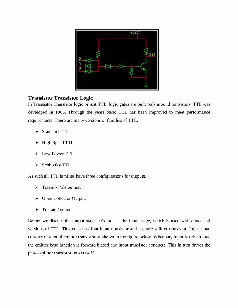
Transistor Transistor Logic
In Transistor Transistor logic or just TTL, logic gates are built only around transistors. TTL was
developed in 1965. Through the years basic TTL has been improved to meet performance
requirements. There are many versions or families of TTL.
Standard TTL
High Speed TTL
Low Power TTL
Schhottky TTL
As such all TTL families have three configurations for outputs.
Totem - Pole output.
Open Collector Output.
Tristate Output.
Before we discuss the output stage let's look at the input stage, which is used with almost all
versions of TTL. This consists of an input transistor and a phase splitter transistor. Input stage
consists of a multi emitter transistor as shown in the figure below. When any input is driven low,
the emitter base junction is forward biased and input transistor conducts. This in turn drives the
phase splitter transistor into cut-off.

Metal Oxide Semiconductor Logic (PMOS and NMOS) MOS or Metal Oxide Semiconductor logic uses nmos and pmos to implement logic gates. One
needs to know the operation of FET and MOS transistors to understand the operation of MOS logic
circuits transistor does not conduct, and thus output is HIGH. But when input is HIGH,NMOS
transistor conducts and thus output is LOW.
Complementary Metal Oxide Semiconductor Logic CMOS or Complementary Metal Oxide Semiconductor logic is built using both NMOS and
PMOS. Below is the basic CMOS inverter circuit, which follows these rules: NMOS conducts
when its input is HIGH.PMOS conducts when its input is LOW. So when input is HIGH, NMOS
conducts, and thus output is LOW; when input is LOW PMOS conducts and thus output is HIGH.


![Dynamic Binary Analysis and Obfuscated Codesshell-storm.org/talks/sthack2016-rthomas-jsalwan.pdf · moveax, [esp] movebx, [esp-0x4] xoreax,ebx pusheax 10. Example: Virtualization](https://static.fdocuments.us/doc/165x107/612f175b1ecc51586943390d/dynamic-binary-analysis-and-obfuscated-codesshell-stormorgtalkssthack2016-rthomas-.jpg)