Digital Design, Kyung Hee Univ. Registers and...
23
Digital Design, Kyung Hee Univ. 1 Registers and Counters • Clocked sequential circuit = F/Fs and combinational gates • Register • Group of flip-flops (share a common clock and capable of storing one bit of information) • Consist of a group of flip-flops together with gates that affect their operation (data transfer) • Counter • A register that goes through a predetermined sequence of binary states • To produce the prescribed sequence of states • 4 bit register • Loading or updating the register @ positive edge of clock • Output can be sampled at any time • Asynchronously reset by Clear_b
Transcript of Digital Design, Kyung Hee Univ. Registers and...

Digital Design, Kyung Hee Univ.
1
Registers and Counters• Clocked sequential circuit = F/Fs and combinational
gates• Register
• Group of flip-flops (share a common clock and capable of storing one bit of information)
• Consist of a group of flip-flops together with gates that affect their operation (data transfer)
• Counter• A register that goes through a predetermined sequence of
binary states• To produce the prescribed sequence of states
• 4 bit register• Loading or updating the register @ positive edge of clock• Output can be sampled at any time• Asynchronously reset by Clear_b
Digital Design, Kyung Hee Univ.
2
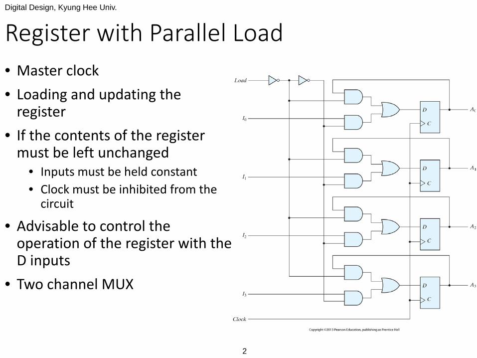
Register with Parallel Load• Master clock• Loading and updating the
register• If the contents of the register
must be left unchanged• Inputs must be held constant• Clock must be inhibited from the
circuit
• Advisable to control the operation of the register with the D inputs
• Two channel MUX
Digital Design, Kyung Hee Univ.
3
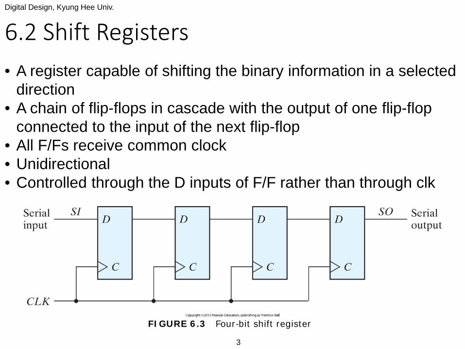
6.2 Shift Registers• A register capable of shifting the binary information in a selected
direction• A chain of flip-flops in cascade with the output of one flip-flop
connected to the input of the next flip-flop• All F/Fs receive common clock• Unidirectional• Controlled through the D inputs of F/F rather than through clk
FIGURE 6.3 Four‐bit shift register

Digital Design, Kyung Hee Univ.
4
Serial Transfer• In serial mode, one bit information is transferred and manipulate at a
time• In parallel mode, all bits is transferred simultaneously during 1 clk
FIGURE 6.4 Serial transfer from register A to register B
Digital Design, Kyung Hee Univ.
5
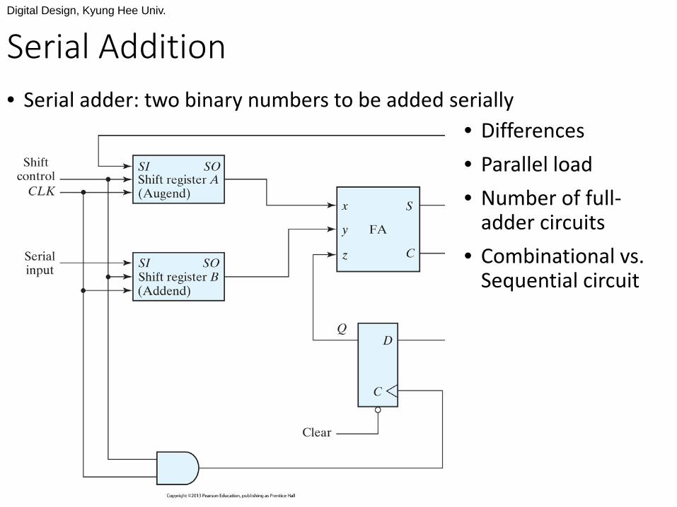
Serial Addition• Serial adder: two binary numbers to be added serially
• Differences• Parallel load• Number of full-
adder circuits• Combinational vs.
Sequential circuit

Digital Design, Kyung Hee Univ.
6
Sequential Circuit Design

Digital Design, Kyung Hee Univ.
7FIGURE 6.6 Second form of serial adder
Digital Design, Kyung Hee Univ.
8
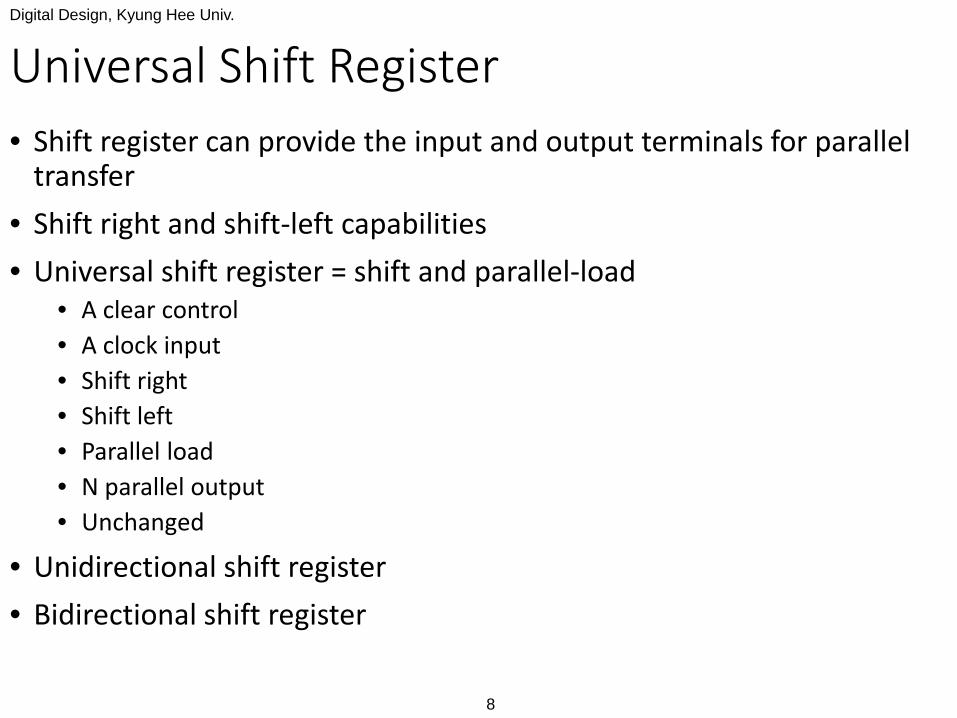
Universal Shift Register• Shift register can provide the input and output terminals for parallel
transfer• Shift right and shift-left capabilities• Universal shift register = shift and parallel-load
• A clear control• A clock input• Shift right• Shift left• Parallel load• N parallel output• Unchanged
• Unidirectional shift register• Bidirectional shift register
Digital Design, Kyung Hee Univ.
9
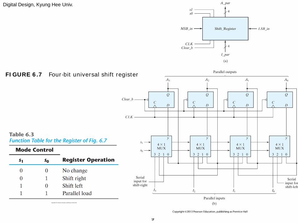
FIGURE 6.7 Four‐bit universal shift register

Digital Design, Kyung Hee Univ.
10
6.3 Ripple Counters• Counter: a register goes through a prescribed sequence of states upon
the application of input pulses • Input pulses: clock pulses or external source (at a fixed interval of time
or at random)• Sequence: binary number sequence or any other sequence of states• N bit binary counter: n flip-flops, count in binary from 0 through 2n-1
• Ripple counters: F/F output transition serves as a source for triggering other F/F (C is not common clock pulse)
• Synchronous counters: C inputs of all F/F receive the common clock

Digital Design, Kyung Hee Univ.
11
Binary Ripple Counter• A series connection of complementing F/Fs
• JK flip-flop (input tied)• T flip-flop
• Receive the incoming count pulses at the least significant bit (0011 → 0100)
• Binary countdown counter• Positive edge of clock

Digital Design, Kyung Hee Univ.
12
BCD Ripple Counter• A sequence of 10 states and return to 0
(binary code with four bits)• Asynchronous sequential circuit

Digital Design, Kyung Hee Univ.
13
Three-decade Decimal BCD Counter
FIGURE 6.11 Block diagram of a three‐decade decimal BCD counter
Digital Design, Kyung Hee Univ.
14
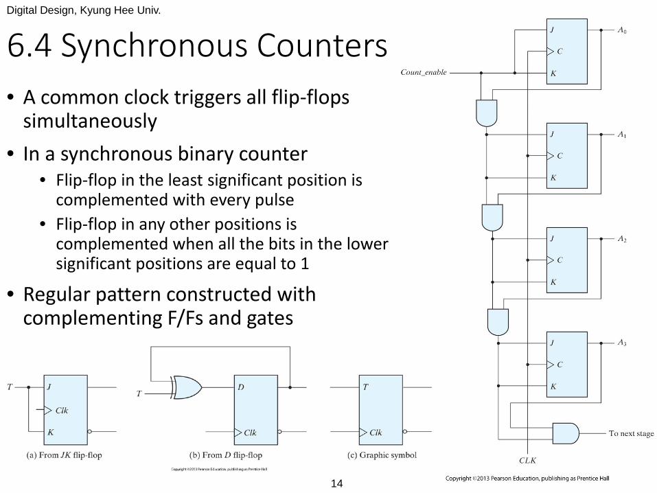
6.4 Synchronous Counters• A common clock triggers all flip-flops
simultaneously• In a synchronous binary counter
• Flip-flop in the least significant position is complemented with every pulse
• Flip-flop in any other positions is complemented when all the bits in the lower significant positions are equal to 1
• Regular pattern constructed with complementing F/Fs and gates

Digital Design, Kyung Hee Univ.
15
Up-Down Binary Counter• A synchronous countdown binary counter
• Flip-flop in any other positions is complemented when all the bits in the lower significant positions are equal to 0
• Inputs to the AND gates must come from the complemented outputs instead of normal
• Up-Down Counter• Up input = 1 → up count• Down input = 1 → down count• Up and down inputs = both 0 → no change• Up and down inputs = both 1 → up count• Up input has priority over the down input
Digital Design, Kyung Hee Univ.
16
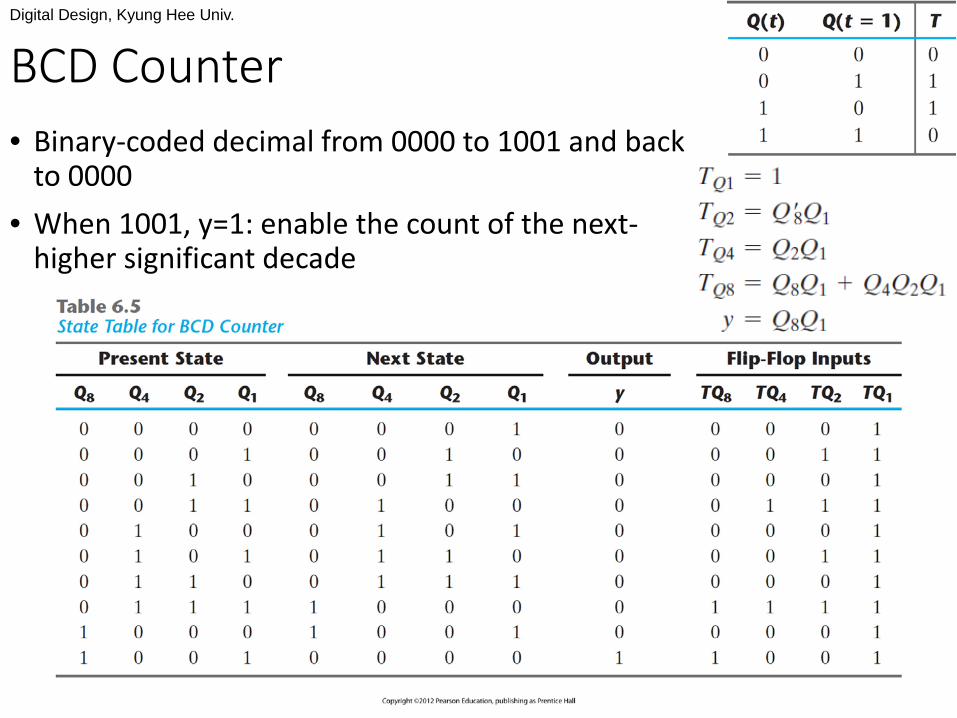
BCD Counter• Binary-coded decimal from 0000 to 1001 and back
to 0000• When 1001, y=1: enable the count of the next-
higher significant decade

Digital Design, Kyung Hee Univ.
17
Binary Counter with Parallel Load• Parallel-load capability for
transferring an initial binary number into the counter prior to the count operation

Digital Design, Kyung Hee Univ.
18
BCD Counter using a Counter with Parallel Load
Digital Design, Kyung Hee Univ.
19
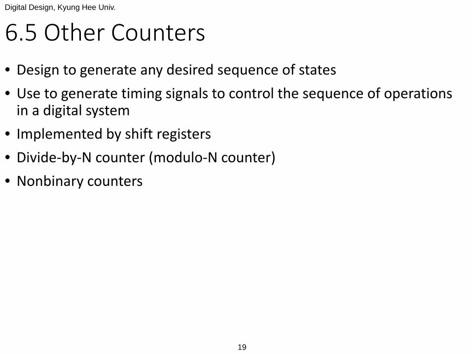
6.5 Other Counters• Design to generate any desired sequence of states• Use to generate timing signals to control the sequence of operations
in a digital system• Implemented by shift registers• Divide-by-N counter (modulo-N counter)• Nonbinary counters

Digital Design, Kyung Hee Univ.
20
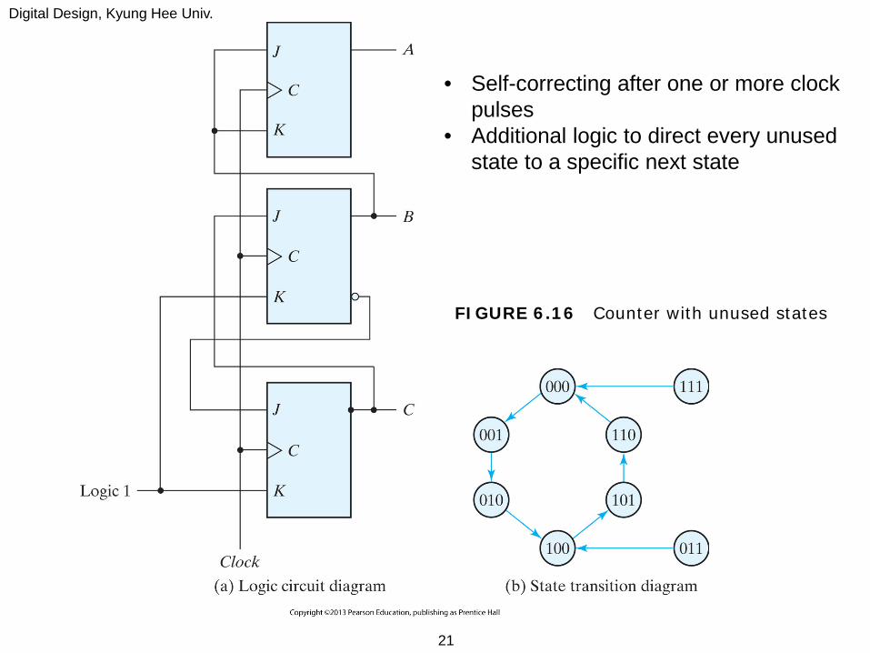
Counter with Unused States• Use fewer than the maximum possible number of states for N F/F (<2n)• For unused states
• Treated as don’t care conditions• Assigned specific next states
Digital Design, Kyung Hee Univ.
21
FIGURE 6.16 Counter with unused states
• Self-correcting after one or more clock pulses
• Additional logic to direct every unused state to a specific next state

Digital Design, Kyung Hee Univ.
22
Ring Counter• To produce the sequence of
timing signals• To generate 2n timing signals1. By a circular shift register with
only one F/F being set at any particular time• Initial value: 1000• Preset/Clear Flip-flops• Shift register with 2n flip-flops
2. By a counter with a decoder• n-bit binary counter together with
an n-to-2n-line decoder
Digital Design, Kyung Hee Univ.
23
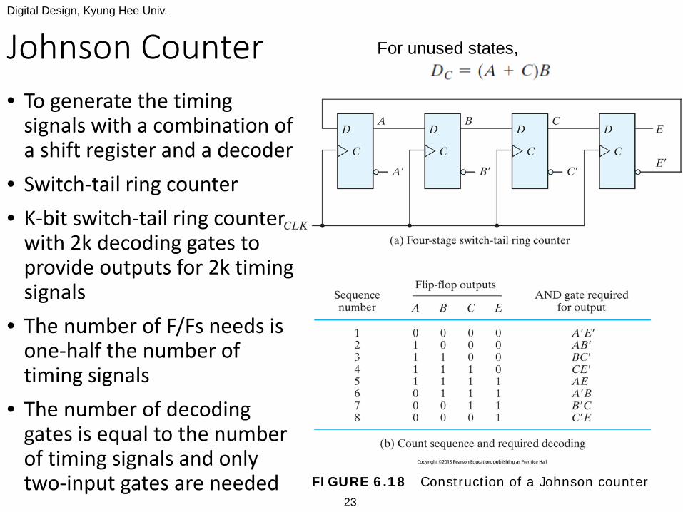
Johnson Counter• To generate the timing
signals with a combination of a shift register and a decoder
• Switch-tail ring counter• K-bit switch-tail ring counter
with 2k decoding gates to provide outputs for 2k timing signals
• The number of F/Fs needs is one-half the number of timing signals
• The number of decoding gates is equal to the number of timing signals and only two-input gates are needed FIGURE 6.18 Construction of a Johnson counter
For unused states,