digital bias
62
Univers ity of Windsor Scholarship at UWindsor Electronic eses and Dissertations 1-1-2010 Digital Control in Tube Power Amplifers Carl Chute University of Windsor , chute@uwindsor. ca Follow this and additional works at: hp://scholar.uwindsor.ca/etd is online database contains the full-text of PhD dissertations and Masters’ theses of University of Windsor students from 1954 forward. ese documents are made available for personal study and research purposes only, in accordance with the Canadian Copyright Act and th e Creative Commons license—CC BY-NC-ND (Aribution, Non-Commer cial, No Derivative Works ). Under this license, works must always be aributed to the copyright holder (original author), cannot be used for any commercial purposes, and may not be altered. Any other use would require the permission of the copyright holder. Students may inquire about wit hdrawing their dissertation and/or t hesis from this database. For additional inquiries, please contact the repository administrator via email ( [email protected] ) or by telephone at 519-253-3000ext. 3208. Recommended Citation Chute, Carl, "Digital Control in Tube Power Ampliers" (2010). Electronic Teses and Di ssertations. Paper 119.
Transcript of digital bias
8/14/2019 digital bias
http://slidepdf.com/reader/full/digital-bias 1/62
University of Windsor
Scholarship at UWindsor
Electronic eses and Dissertations
1-1-2010
Digital Control in Tube Power AmplifersCarl ChuteUniversity of Windsor , [email protected]
Follow this and additional works at: hp://scholar.uwindsor.ca/etd
is online database contains the full-text of PhD dissertations and Masters’ theses of University of Windsor students from 1954 forward. ese
documents are made available for personal study and research purposes only, in accordance with the Canadian Copyright Act and the Creative
Commons license—CC BY-NC-ND (Aribution, Non-Commercial, No Derivative Works). Under this license, works must always be aributed to the
copyright holder (original author), cannot be used for any commercial purposes, and may not be altered. Any other use would require the permission of
the copyright holder. Students may inquire about withdrawing their dissertation and/or thesis from this database. For additional inquiries, please
contact the repository administrator via email ([email protected]) or by telephone at 519-253-3000ext. 3208.
Recommended CitationChute, Carl, "Digital Control in Tube Power Ampliers" (2010). Electronic Teses and Dissertations. Paper 119.

8/14/2019 digital bias
http://slidepdf.com/reader/full/digital-bias 2/62
Digital Control in Tube Power Amplifiers
by
Carl Chute
A Thesis
Submitted to the Faculty of Graduate Studies through the
Department of Computer and Electrical Engineering in partial fulfillment
of the requirements for the Degree of Master of Applied Science at the
University of Windsor
Windsor, Ontario, Canada
August 2010

8/14/2019 digital bias
http://slidepdf.com/reader/full/digital-bias 3/62
© 2010 Carl Chute
All Rights Reserved. No part of this document may be
reproduced, stored or otherwise retained in a retrieval
system or transmitted in any form, on any medium or by any
means without the prior written permission of the author.

8/14/2019 digital bias
http://slidepdf.com/reader/full/digital-bias 4/62
Digital Control In Tube Power Amplifiers
By: Carl Chute
Approved by:
____________________________________
Dr. Edwin Tam (External Reader)
____________________________________
Dr. H. Wu (Internal Reader)
____________________________________
Dr. Roberto Muscedere (Advisor)
____________________________________
Dr. M. Mirhassani (Chair)
August 2010

8/14/2019 digital bias
http://slidepdf.com/reader/full/digital-bias 5/62
iv
Declaration of Originality
I hereby certify that I am the sole author of this thesis and that no part of this thesis
has been published or submitted for publication.
I certify that, to the best of my knowledge, my thesis does not infringe upon anyone’s
copyright nor violate any proprietary rights and that any ideas, techniques, quotations, or any
other material from the work of other people included in my thesis, published or otherwise,
are fully acknowledged in accordance with the standard referencing practices. Furthermore,
to the extent that I have included copyrighted material that surpasses the bounds of fair
dealing within the meaning of the Canada Copyright Act, I certify that I have obtained a
written permission from the copyright owner(s) to include such material(s) in my thesis and
have included copies of such copyright clearances to my appendix.
I declare that this is a true copy of my thesis, including any final revisions, as
approved by my thesis committee and the Graduate Studies office, and that this thesis has not
been submitted for a higher degree to any other University or Institution.

8/14/2019 digital bias
http://slidepdf.com/reader/full/digital-bias 6/62
v
Abstract
Vacuum tubes are an old technology with a very important use in the audio electronics
industry. They have a comparatively short life cycle and must be replaced often. This is a
burden for the consumer since they must then calibrate (bias) the new set of tubes. This
exposes the consumer to potentially lethal voltages. If the bias is not set correctly the tubes
could be destroyed or the amplifier could operate inefficiently.
The work presented in this thesis describes a digital control system that maintains optimum
biasing for any tube used in the power amplifier. This system automatically determines the
ideal bias voltage every time the amplifier is turned on. Unlike other designs, this system iscompletely non-intrusive and does not affect audio quality. The system requires no consumer
maintenance and has nearly eliminated the burden of replacing the tubes in an audio power
amplifier.

8/14/2019 digital bias
http://slidepdf.com/reader/full/digital-bias 7/62
vi
Acknowledgements
I would like to thank the following people for their help and support with this project; My
advisor Dr. Roberto Muscedere, my committee members Dr. Edwin Tam and Dr. H. Wu, the
ECE department graduate secretary Andria Ballo, and departmental technologist Frank
Cicchello.
I would also like to thank Mitacs Canada and Chute Amps Inc. for their financial support and
use of facilities and equipment.

8/14/2019 digital bias
http://slidepdf.com/reader/full/digital-bias 8/62
vii
Table of Contents
Declaration of Originality ........................................................................................................ iv
Abstract......................................................................................................................................v
Acknowledgments.................................................................................................................... vi
List of Figures .......................................................................................................................... ix
List of Tables ............................................................................................................................ x
Chapter 1 Introduction............................................................................................................1
1.1 History....................................................................................................................... 1
1.2 The Problem.............................................................................................................. 1
Chapter 2 Background and Literature Review .......................................................................2
2.1 Introduction............................................................................................................... 2
2.2 Operation of Power tubes.......................................................................................... 2
2.3 Literature Review...................................................................................................... 5
2.4 The Reference Amplifier .......................................................................................... 6
Chapter 3 Designing an adaptive circuit...............................................................................12
3.1 Introduction............................................................................................................. 12
3.2 Control Circuit types............................................................................................... 12
3.3 Designing the Circuit .............................................................................................. 13
3.4 Software Algorithms............................................................................................... 24
Chapter 4 Testing and Performance Results.........................................................................30
4.1 Introduction............................................................................................................. 30
4.2 Accuracy Test – Delay Algorithm .......................................................................... 30
4.3 Accuracy Test – Averaging Algorithm................................................................... 31
4.4 Accuracy Test- Main System.................................................................................. 33
Chapter 5 Conclusions and Recommendations ....................................................................37

8/14/2019 digital bias
http://slidepdf.com/reader/full/digital-bias 9/62
viii
5.1 Summary and Contributions ................................................................................... 37
5.2 Recommendations for Future Work........................................................................ 37
References................................................................................................................................39
Appendix A..............................................................................................................................40
Vita Auctoris............................................................................................................................51

8/14/2019 digital bias
http://slidepdf.com/reader/full/digital-bias 10/62
ix
List of Figures
Figure 2.1: Terminals and Current Paths of a Power Pentode...................................................3
Figure 2.2: The Power Supply ...................................................................................................9
Figure 2.3: Test Fixture Schematic..........................................................................................11
Figure 3.1: General Algorithm.................................................................................................14
Figure 3.2: Sampling Circuit Schematic..................................................................................15
Figure 3.3: Relay Isolation Circuit...........................................................................................19
Figure 3.4: Screen Current Compensation Circuit...................................................................22
Figure 3.5: Microcontroller Development Board and Sampling Circuitry..............................23
Figure 3.6: System Gain Algorithm.........................................................................................26
Figure 3.7: Averaging Subroutine............................................................................................28
Figure 4.1: The Completed Prototype......................................................................................30
Figure 4.2: Debugger Interface................................................................................................32
Figure 4.3: Tube Test Data ......................................................................................................36

8/14/2019 digital bias
http://slidepdf.com/reader/full/digital-bias 11/62
x
List of Tables
Table 2.1: Requirements for the Different Tube Types.............................................................7
Table 3.1: Resistor Values .......................................................................................................18
Table 4.1: Averaged Results....................................................................................................33
Table 4.2: Tube Types used for Testing ..................................................................................34
Table 4.3: Tests........................................................................................................................35

8/14/2019 digital bias
http://slidepdf.com/reader/full/digital-bias 12/62
1
Chapter 1 Introduction
1.1 History
Vacuum tubes are the predecessor to the modern transistor. Before the 1960’s they were usedin nearly every electronic device; televisions, radios, and computers. There are several
different types of vacuum tubes: diodes, triodes, tetrodes, and pentodes. Diodes and triodes
are typically used for rectification and small signal amplification, whereas tetrodes and
pentodes are used for power amplifiers (audio speaker drivers, radio transmitters, and
microwaves). The task of a power amplifier is to provide a fixed level of gain to a processed
signal and deliver power into a load such as a loudspeaker [1]. For the purposes of this work,
a tetrode is the same as a pentode, and both will referred to as power tubes. Most power tubes
have been replaced by the modern transistor, although these tubes still hold a very important
application in the audio amplifier industry.
1.2 The Problem
Audio amplifiers based on power tubes have become increasingly popular in the past ten
years despite the large production of solid state (transistor) amplifiers. This is because they
produce purer sounds which are more pleasing to the human ear. Tube audio power
amplifiers are used almost exclusively by pro guitarist and bass players. These amplifiers are
used at nearly every professional music production and recording studio. Power tube
production in the world is very limited as the vast majority of them are manufactured in
Eastern Europe and Russia, in facilities that have been in operation since the 1940’s. This
variance in production creates very unpredictable results in terms of sound quality making it
difficult for high end audio manufacturers to have consistent and favourable production
quality. Power tubes by nature run at very high temperatures. The thermal stress will change
the alignment and shape of metal components in the tube. This will inevitably change theoperating characteristics of the tube over its lifetime. Since it is not possible to change the
way these tubes are being used and manufactured, circuits must be designed to be adaptive to
accommodate this variance and allow each amplifier to run optimally.

8/14/2019 digital bias
http://slidepdf.com/reader/full/digital-bias 13/62
2
Chapter 2 Background and Literature Review
2.1 Introduction
In this chapter the fundamental operation of power tubes will be reviewed along with areview of prior research. This review will give a fundamental understanding of the basic
concepts that will be used with the adaptive circuit design developed in this thesis. The
amplifier constructed for testing the adaptive circuit is also examined as each component of
the amplifier is directly linked to the adaptive biasing circuit.
2.2 Operation of Power tubes
Power pentodes (see Figure 2.1) are five terminal devices that are used to amplify power and
drive loudspeakers. The five terminals are the Anode, Cathode, Grid, Screen Grid, and
Suppressor Grid. There are also two terminals for the heater, which is used to heat the
cathode allowing the thermionic emission. There are many resources available on the physics
of pentode operation, therefore a very simple overview is provided for understanding of the
material in this thesis.
When the cathode of a power pentode is heated a cloud of electrons form around it. The
electrons will flow towards the positively charged anode and screen grid. A grid is placedbetween the cathode and the anode/screen grid to control how many electrons flow. If the
grid voltage is very negative no electrons will flow. If the grid voltage is close to 0 V, many
electrons will flow. By modulating the grid voltage you can vary the large anode current and
produce amplification. Most of the electrons from the cathode go to the anode, while
approximately 10% of them go to the screen grid. Although the real physics of a power
pentode are slightly more complicated, this explanation will provide a good basis for DC
biasing. Note that the only difference between a pentode and a tetrode is that a pentode has a
suppressor grid to mitigate parasitic capacitance. In terms of DC calculations, they can be
treated as the same device.

8/14/2019 digital bias
http://slidepdf.com/reader/full/digital-bias 14/62
3
Figure 2.1: Terminals and Current Paths of a Power Pentode
2.2.1 Bias Types
Each power tube requires a DC bias voltage to function correctly. A bias voltage is applied
between two terminals of the tube and essentially controls how much power the tube is going
to consume/deliver at idle. If the bias is too high, the tube will overheat and inevitably
destroy itself. Where as if the bias is too low, the output signal will be weak and the tube will
run inefficiently. A perfect bias point must be found to ensure that the power tubes are
running safely at their full potential. Audio amplifiers today use three topologies for biasing;
each with their inherent problems:
Preset Bias Designs
Preset bias designs are not adjustable by the user and the bias point is the same for every tube
used in the amplifier. The grid voltage is fixed, and valve current is determined purely by
valve characteristics, so there is no protection against over-current, or compensation for
changes in valve characteristics with age [1]. This is generally a poor scheme as all tubes
have inherent variances from manufacturing. In order for them to run optimally each tube
needs a uniquely calibrated bias voltage.
Adjustable bias designs
Adjustable bias designs mitigate the previous problem by allowing the consumer to adjust the
bias voltage with a set screw or knob system. This allows the power tubes to run within safe

8/14/2019 digital bias
http://slidepdf.com/reader/full/digital-bias 15/62
4
limits, however the bias point may not be optimal since it was selected by the consumer. This
topology can also be very dangerous as the consumer is required to disassemble the amplifier
and monitor high voltages (>400 V) while the system is fully powered. Since the life span of
a power tube can be short, this must be done every time the tubes are replaced. This can be
quite the burden for the consumer. Another option is to send the amplifier back to the
manufacturer for tube replacement and calibration, though very few will do this as it is quite
costly.
Cathode Bias designs
Cathode biased designs use an AC bypassed power resistor to set a positive voltage at the
cathode. The grid of the tube is DC grounded so the grid to cathode voltage still remains
negative. This topology has a self limiting feature; as the cathode current increases, so does
the bias voltage, hence decreasing the cathode current. This type of bias is very inefficient
and generally results in a less than 50% power output ratio. This is mainly contributed to the
large loss of power in the cathode bias resistor.
2.2.2 Optimum Bias Point
The optimum bias point for a pair of power tubes in push-pull configuration is 70% anode
dissipation at idle. This value has been determined experimentally and is the industry
standard ‘rule of thumb’. Biasing an amplifier at or above 80% dramatically decreases the
tubes lifespan, while biasing at or below 60% produces a noticeably weak audio power
output.
Biasing at idle means that when there is no AC signal applied to the tube grid, the power
dissipated in its anode is 70% of its maximum dissipation rating. For Example, EL34 tubes
have a maximum dissipation rating of 25 W. This mean that at idle they should dissipate
0.70 x 25 W = 17.5 W. So if a pair of EL34s is running at 400 V the idle bias current should
be set to 17.5 W/400 V = 43.75 mA per tube or 87.5 mA total. Note that this is the value of
the anode current, which is not the same as the cathode current (cathode current is the sum of
the screen current and anode current).

8/14/2019 digital bias
http://slidepdf.com/reader/full/digital-bias 16/62
5
2.2.3 The Screen Grid
Screen grid current must be subtracted from the cathode current to get the true anode current
(and hence the true anode dissipation). Screen grid current varies depending on the screen
grid resistor, the screen grid voltage, and the transconductance of the tube. The screen grid
current is typically 5%-10% of the anode current. This is treated as a known constant since
the screen grid current variance amongst tubes for a given condition (supply voltage/screen
grid resistor) is negligible.
2.3 Literature Review
There has been no prior research in digital control for tube audio power amplifiers
specifically, however there have been a number of papers done on projects with similaraspects. These papers are summarized below.
2.3.1 A Simple Direct-Coupled Power MOSFET Audio Amplifier Topology Featuring Bias
Stabilization
This paper [2] introduced an automated bias control for a 200 W MOSFET audio power
amplifier; this was at a time when FET power sections were new. The automated bias control
was needed to stabilize the large temperature variance inherent in FETs. So although this is
not a tube amplifier, both devices can change their operating characteristics over time and
between devices. The bias scheme presented does not possess memory and therefore must
continuously be sampling the FET current. The authors showed that it is somewhat difficult
to sample the DC current since there is a large AC current swing present when the amplifier
is in use. Overall the circuit had good performance, but it was intrusive since it always had
the sampling circuitry in the audio signal path.
2.3.2
Class AB Large Swing CMOS Buffer Amplifier with Controlled Bias Current
This paper [3] presented an automated bias control for a 4.7 mW 1.2 µm CMOS buffer
amplifier. This amplifier was designed to drive telecommunication lines at voice frequencies
and uses continuous sampling and a DC servo to control the CMOS bias current. The major
difference with this approach is that it is built on an integrated circuit so a different sampling

8/14/2019 digital bias
http://slidepdf.com/reader/full/digital-bias 17/62
6
approach was used. In this case the authors used a diode connected transistor to sample the
current. Once again this circuit performed well but utilized intrusive sampling.
2.3.3 Digital Control System for the Thermionic Cathode in an Electron Gun
Though not directly related to audio electronics, this paper [4] presents a modern digital
control system for a thermionic cathode (audio tubes also use thermionic cathodes). The
authors used a microprocessor to control the current in the cathode to prevent it from
destroying the electron gun. The system uses a photo-sensor to sample the current which is
then sent through an analog-to-digital converter (ADC) and processed by the microprocessor.
The output is sent through a digital-to-analog converter (DAC) and is used to control the
cathode’s heating source. This system is analogous to what will be used for audio tubes
except that this system utilizes continuous sampling (which is acceptable for electron gun
applications). This paper demonstrates how a microprocessor can be used to intelligently
control a closed loop system.
2.4 The Reference Amplifier
In order to test the proposed adaptive circuit, a reference amplifier is constructed.
2.4.1 System Parameters
This amplifier was designed to accommodate the three different tube types available. The test
fixture consists of a push pull power amplifier including a phase inverter/driver circuit for
ease of testing. Table 2.1 is a summary of the requirements for the different tube types. The
test fixture is designed around these parameters.

8/14/2019 digital bias
http://slidepdf.com/reader/full/digital-bias 18/62
7
Tube Type KT77 6L6 EL34
Supply Voltage 800 Vmax 500 Vmax 800 Vmax
Anode Dissipation 25 W 30 W 25 W
ReflectedImpedance ~3200 ohm ~3400 ohm ~3200 ohm
Heater Current 1.4 A 0.9 A 1.5 A
Screen Voltage 800 Vmax 450 Vmax 450 Vmax
Rg2 1000 ohm 1000 ohm 1-2 kohm
Bias Voltage -10 V to -40 V -10 V to -40 V -10 V to -40 V
Table 2.1: Requirements for the Different Tube Types
2.4.2 Power Supply
The power supply was designed to accommodate the maximum supply loads. In this case an
anode supply voltage of 400 V was targeted. This is suitable for all the tube types and is a
typical anode voltage in musical amplifiers with these types of tubes.
The appropriate supply current was determined by examining the maximum load amongst the
tubes. Each 6L6 is capable of dissipating 30 W. This requires 30 W / 400 V = 75 mA per
tube. Therefore the power supply was designed for 200 mA, the extra 50 mA is used toaccommodate preamp circuitry and screen grid currents.
A Hammond 272HX was chosen to meet these requirements. The 272HX has a 600 VCT
winding that can accommodate 200 mA [5]. It also has a 6.3 VCT winding that can
accommodate 6 A, this winding is used for the heaters.
The power supply has 3 voltage points: a main anode voltage of ~400 V at 150 mA, a screen
grid voltage of ~380 V at 20 mA, and a phase inverter voltage of ~320 V at 2 mA.
It is important to note that these are just target voltages and that they will change depending
on which tube is loading the supply.
A negative voltage power supply is needed to bias the grids of the power tubes from -40 V to
-10 V. This is done with a half wave rectifier from the main high voltage winding. A half

8/14/2019 digital bias
http://slidepdf.com/reader/full/digital-bias 19/62
8
wave rectifier is used for simplicity since the current draw from this source is very small
(very little current will flow into the power tube grids). A capacitive network and a linear
potentiometer are included to manually adjust the bias voltage. This potentiometer will later
be replaced by the output control circuit from the microcontroller.
A low voltage power supply is needed to operate the microcontroller, relays, op-amps, and
other ICs. The total load for this supply varies depending on how many relays are active,
though the worst case load does not exceed 1 A. A bridge rectifier is used in conjunction with
a fixed 5 Volt regulator to provide a constant and stable supply voltage under varying load
conditions [6]. Initially this network was connected to the extra 5 VAC supply provided by
the 272HX. Unfortunately the regulator input voltage was not high enough to be stable in all
conditions. The network was connected to the 6.3 VAC heater winding to provide a higher
regulator input voltage and a constant 5 V output.
A mains fuse is included in this test fixture for safety and protection purposes. At full load
the amplifier will be drawing approximately 200 mA x 400 V = 80 VA from the main
winding and 3 A x 6.3 V + 1 A x 5 V = 23.9 VA from the heater winding. The total normal
load is thus ~100 VA. A 2 A fuse was chosen for the transformer primary, this will activate if
the circuit draws approximately twice of its normal VA rating and will provide good
protection against faults. Figure 2.2 shows the power supply design.

8/14/2019 digital bias
http://slidepdf.com/reader/full/digital-bias 20/62
9
Figure 2.2: The Power Supply

8/14/2019 digital bias
http://slidepdf.com/reader/full/digital-bias 21/62
10
2.4.3 Output Stage
Unlike transistor amplifiers, tube power amplifiers require an output transformer to couple
the power from the high impedance power tubes to the low impedance speakers. Tube
amplifiers are sensitive to impedance matching. An unmatched load will operate the tube in
an unsafe dissipation region and will cause its destruction. For this push pull stage an output
transformer was chosen that can accommodate the three different tube types. The 6L6, EL34,
and KT77 have similar requirements (3200 ohm) .The Hammond 1750N is ideal for this
application. It has a 3200 ohm primary and a 4-8-16 ohm secondary [7]. It can handle 50 W
of continuous audio power which is well suited for this high power amplifier
2.4.4 Phase Inverter
The phase inverter is necessary in a push pull amplifier as it delivers signals of opposite
phase to each of the power tubes. The phase inverter also acts as a driver as it amplifies a line
level signal up to the point where it can drive a power tube grid. The details of phase inverter
operation are quite lengthy, so they will not be discussed in detail. A standard “long tail
phase inverter” design was chosen and attached to the power section as shown in Figure 2.3.

8/14/2019 digital bias
http://slidepdf.com/reader/full/digital-bias 22/62
11
Figure 2.3: Test Fixture Schematic

8/14/2019 digital bias
http://slidepdf.com/reader/full/digital-bias 23/62
12
Chapter 3 Designing an adaptive circuit
3.1 Introduction
This chapter examines the design of the adaptive bias circuit. The hardware design ispresented followed by the software design. Each step of the process is detailed, including the
background research and unsuccessful designs.
3.2 Control Circuit types
The main challenge of this work is to design a circuit that will hold the bias voltage at an
optimum point. The exact point should be easily configurable so that so that it will function
with a range of supply voltages. The following are several possible approaches to explore in
designing this circuit.
DC Servo Control Circuit
This is the simplest approach to implement as it involves continuous monitoring of the tubes
cathode current and instantaneous adjustment (using op-amps and analog circuitry). This type
of bias control is already implemented in modern amplifier design [2]. The main problem is
that it involves continuous sampling which induces a load on the power amplifier which
produces unfavourable audible results. The goal of this thesis is to produce a totally
transparent circuit, therefore a different approach is required.
Analog Sample and Hold
This approach requires sampling the cathode current and holding its value in an analog
network; generally through capacitors. The sampling circuit can then be disconnected from
the power amplifier therefore solving the prior transparency issue. The held current value can
be used to adjust the bias voltage using analog computation. This approach would have been
feasible when microprocessors were relatively expensive and overall costs were high., Today
however it is the opposite where the cost to implement the analog computation and holding
circuitry far exceeds that of the cost of microprocessor.

8/14/2019 digital bias
http://slidepdf.com/reader/full/digital-bias 24/62
13
Microcontroller Sample and Hold
The final approach requires using an ADC to store and process the cathode current value in
the microcontroller. The microcontroller can use an algorithm to determine how the output
bias voltage must change. The microcontroller will continue sampling this value until it
determines what output value it should hold. Once all the computations and comparisons
have been made, the microcontroller can activate a transparency relay and detach the
sampling circuitry from the power amplifier. This method also has the advantage of making
intelligent control decisions. For example, it is easy to implement a failure detection circuit
as it would simply require a few lines of code. Other intelligent features can easily be added
to the system as the microcontroller can be reprogrammed with simplicity. This avenue is not
always easy with analog control circuits as it generally requires a physical change to the
circuit.
3.3 Designing the Circuit
It was decided to use the microcontroller circuit as it offers the most promise, expandability,
and minimal cost.
3.3.1 Signal Processing Algorithm
The signal processing algorithm is a basic feedback loop. The system examines the input
value and compares it to a range of ideal values. If that input value is not within the range of
acceptable ideal values, then the microcontroller adjusts the output accordingly. Once the
input value is ideal, the microcontroller stores the resulting output and detaches the sampling
circuit from the power tubes. This stored value will be used as a starting point each time the
amplifier is turned on. Figure 3.1 shows a flow chart of this algorithm.

8/14/2019 digital bias
http://slidepdf.com/reader/full/digital-bias 25/62
14
Power On
Set TransparencyRelay / Load Initial
Output
Delay
Get ADC Value
ADC Value >
Vmax?
Increment Output
Value
ADC Value <
Vmin?
Decrement Output
Value
Delay
Hold Value / Clear
Transparency
Figure 3.1: General Algorithm
3.3.2 The Sampling Circuit
The sampling circuit consists of a very small and accurate resistor tied to the cathode of both
power tubes in the amplifier. The resistor is bypassed by the transparency resistor when not
in the sampling mode. It is important that the sampling resistor is small as a large sampling
resistor will create inaccurate bias points when the circuit changes out of sampling mode.
The reason for this is that the total cathode current path will have an extra resistance in series

8/14/2019 digital bias
http://slidepdf.com/reader/full/digital-bias 26/62
15
when sampling. A 1 ohm resistor is suitable and will not significantly change the bias current
when not in sampling mode.
The combined DC cathode current will be somewhere between 70 mA and 140 mA for all
types of tubes. This range accounts for anode dissipation between 50% and 100% of the max
dissipation rating. With a 1 ohm sampling resistor the analog sampling signal will be
between 0.07 V and 0.14 V.
The built-in ADC has an 8-bit sampling resolution which is linearly defined between 0 V and
the microcontroller supply voltage of 5 V. This translates to an incremental resolution of
0.02 V. Based on the sampled voltage of 0.07 V to 0.14 V, this would only allow for 5
distinct input values. To increase the resolution of the input sampling, the signal is then
multiplied by 34 and offset to obtain a signal between 0 V and 4.76 V into the ADC, thus
using the full input resolution. Figure 3.2 shows the complete sampling circuit.
Figure 3.2: Sampling Circuit Schematic

8/14/2019 digital bias
http://slidepdf.com/reader/full/digital-bias 27/62
16
3.3.3 The Transparency Relay
A high current relay is required to disconnect the sampling circuitry from the amplifier once
a proper bias has been established. It must also bypass the sampling the resistor. Since it is
bypassing the sampling resistor all of tubes current will flow through the relay. The relay
must be able to handle 200 mA and have a dual pole, dual throw configuration.
3.3.4 Bias Voltage Output Types
The microcontroller control network must process the input sampling voltage and output a
bias voltage for the power tubes. The bias voltage can range between -10 V and -40 V, and
will be adjusted using a variable resistance. To control this voltage the microcontroller must
be fully isolated from the high voltage negative supply. There are several differentapproaches to this:
High Voltage Digital Potentiometer
A high voltage digital potentiometer would be an ideal and simple solution to the isolation
problem. Unfortunately the highest commercially available voltage rating is only 30V. Since
the output bias voltage needs to go as low as -40 V this device could not be controlled by a
digital signal between 0 V and 5 V.
This device could be used if it was placed under a different supply reference. For example,
the ground of the device could be set at -40 V and the positive terminal at -10 V. This would
allow full voltage control over the needed range while keeping the device within voltage
limits. The problem unfortunately is that the digital control signals from the microcontroller
must also be isolated into the -40 V to -10 V reference. This would have to be done with
opto-couplers or solid state relays; a very costly requirement in hardware which is not
feasible compared to the other approaches listed.
Motorized Potentiometer
A motorized potentiometer uses a DC motor to remotely control the wiper of a
potentiometer. These devices are also very expensive and are difficult to control in order to

8/14/2019 digital bias
http://slidepdf.com/reader/full/digital-bias 28/62
17
obtain accurate results. It would also require a DAC to interface the motor to the
microcontroller; a component not typically included within the microcontroller.
Opto-Coupler
Opto-couplers use a photo-resistor coupled to a LED to vary the output resistance based on
how bright the LED is. Opto-couplers are relatively inexpensive but are too difficult to
control accurately. These devices are typically either ON or OFF and the resistive range in
between is very sensitive and varies greatly between components. These devices also require
a DAC converter to interface to the microcontroller.
Power FET
An analog voltage signal can be applied to the gate of a power FET to control how much
current it outputs. This current can then be used to create the bias voltage. This device would
be difficult to control as it would depend on the very specific device curve traces of the
transistor which are very nonlinear. It would also require a DAC converter to drive the gate
signal.
Solid State Relays
Solid state relays can be used to bypass resistors in a string of resistance. This is very easy to
do and does not require a DAC converter. These devices are inexpensive and can handle high
voltages [8]. This string of resistors can be physically larger, however this is acceptable
considering the size of the overall amplifier.
The solid state relays approach was chosen as it offered the best solution with the least
possible problems. The relays were arranged in a chain to bypass different resistance values.
This effectively changes the value of a resistive divider therefore adjusting the bias voltage.
The overall resistance of the string needs to be ~25 kohm. If this is done with 8 different
resistor values there can effectively be 256 different resistance values. Figure 3.3 shows the
circuit while Table 3.1 shows the string of resistors values used in the design with
standardized values which were very similar to the idealized requirements.

8/14/2019 digital bias
http://slidepdf.com/reader/full/digital-bias 29/62
18
Resistor Ideal Value Closest Standard Value
R7 12 k 12 k
R6 6 k 6.2 k
R5 3 k 3 kR4 1.5 k 1.5 k
R3 750 750
R2 375 390
R1 187.5 180
R0 93.75 91
Total Value: 23.9 k 24.1 k
Table 3.1: Resistor Values
When all of the resistors are not bypassed the total resistance is 24111 ohms.

8/14/2019 digital bias
http://slidepdf.com/reader/full/digital-bias 30/62
19
Figure 3.3: Relay Isolation Circuit
Some major problems were encountered while implementing the solid state relay design.
When a mechanical relay is engaged the output shorts whereas a solid state relay enables
current to flow through a triac. There is a voltage drop associated with current flowing
through the output triac (about 1 V). This places an extra 1 V in the potential divider when a
dead short is needed. This problem could be compensated for in software if it was not for the

8/14/2019 digital bias
http://slidepdf.com/reader/full/digital-bias 31/62
20
fact that solid state relays also latch. Essentially if a DC current is flowing through the output
triac, it will not stop conducting until the input signal and the output signal cross zero (which
never happens in DC). Unfortunately this means that once a relay is activated to bypass a
resistor, it will not stop conducting regardless of what input is applied to it. This approach
was deemed inappropriate and another attempt was made.
Mechanical Relays
Mechanical relays are slightly more expensive than solid state relays but provide true short
and open switching (no latching, and no unwanted voltage drops) [9]. This approach was
implemented using the same methodology as the solid state relay.
This mechanical relays approach was found to operate the best and was kept for the finaldesign.
3.3.5 Screen Current Compensation
Screen grid current is usually assumed to be a fixed fraction of the cathode current. However
there are slight variances in this fraction within each specific tube. This current should be
sampled so that the anode current can be accurately calculated. At a fixed operating point, the
screen current can deviate approximately +/- 1 mA between tubes. If a fixed value is used for
the screen current the anode current will deviate +/- 1 mA. At the ideal operation point (70%)
dissipation and a 400 V anode supply, this will vary the dissipation calculation by
1 mA x 400 V = 0.4 W, which is a total variance of 0.4 W/25 W = 1.6% for the EL34/KT77
and 1.3% for the 6L6. This is a small variance overall, so it is important that the hardware
used to compensate for this is inexpensive in every sense otherwise the extra accuracy cannot
be justified on a commercial basis.
Analog Sampler/Subtractor
A high impedance circuit was used to measure the voltage across the screen resistor (sample
at two high voltage points). This voltage essentially indicated the screen current since the
screen resistor is fixed at 1 kohm. High impedance voltage dividers were placed between the
voltage points and ground. It is important that the network was very high impedance since it

8/14/2019 digital bias
http://slidepdf.com/reader/full/digital-bias 32/62
21
is essentially placed in parallel with the power tube. If the network was anything less than
10 Mohm it would have an effect on the sonic quality of the tube. The small voltage from the
high impedance voltage dividers was then fed into buffers, and then into a differential
amplifier to obtain a voltage difference. This voltage difference signal was then fed into
another differential amplifier that subtracted the screen current from the cathode current to
obtain the true anode current. This value was then sampled by the microcontroller.
The circuit functioned, but had too high of a variance to be useful. The inaccuracies in the
op-amps and in the high impedance resistors (1% of 10 Mohms is 100 kohms) gave a range
of variance that defeated the purpose of the circuit.
Digital Subtractor
This approach was very similar to the first except that it eliminated the differential amplifiers
and their variance. The voltage divider signals were fed into buffers then directly to the
microcontroller; the subtraction required was done in software. This approach had the
disadvantage of using more microcontroller ports, however the variance associated with this
circuit was improved, but still defeated the purpose of the circuit
Due to the high variances, neither approach was taken. Instead a fixed screen current value is
assumed. The high impedance sampling is very difficult and expensive to perform accurately.
More relay switching would be necessary to minimize the loading on the audio path by the
sampling circuit. These screen sampling circuits were simply not accurate enough to justify
the extra expense. Figure 3.4 shows the screen current compensation circuit while Figure 3.5
shows the sampling circuitry connected to the Development Board.

8/14/2019 digital bias
http://slidepdf.com/reader/full/digital-bias 33/62
22
Figure 3.4: Screen Current Compensation Circuit

8/14/2019 digital bias
http://slidepdf.com/reader/full/digital-bias 34/62
23
Figure 3.5: Microcontroller Development Board and Sampling Circuitry
3.3.6 Choosing a Microcontroller
With any commercial device, cost is a major consideration. In order to keep costs low, a
microcontroller which meets the needs of the proposed circuit is selected. It has the following
requirements:
• A built in ADC for sampling cathode current
• At least 8 output ports for controlling the bias voltage
• One output port for activating the transparency relay
• A USB interface for programming
• Speed is not critical, therefore it can be low to reduce cost
• Physical size is also not critical and can be sacrificed to further reduce cost

8/14/2019 digital bias
http://slidepdf.com/reader/full/digital-bias 35/62
24
Considering these requirements, a Freescale MC68HC908QY4 was chosen. It is a low cost
8-bit microcontroller [10] that can be purchased in bulk for less than $2.00 a piece. For the
prototype a Softec HC908 development kit [11] (pre-fabricated printed circuit board) will be
used to program the microcontroller and to interface it to the amplifier circuitry.
3.4 Software Algorithms
3.4.1 Former Value Check Algorithm
The microcontroller contains 4096 bytes of non-volatile FLASH memory. Some of this
memory is used to store the calculated output value from the last time the program was run.
This gives a superior starting point, in many cases the program will not even need to perform
any additional analysis. The ideal output value will not change dramatically between powerups, so the adjustment that has to be made will be small (or non-existent). This significantly
reduces the amount of wait time required for this system.
The FLASH memory included on the MC68HC908QY4 cannot be programmed or erased
when it is running user code from the flash memory [10]. The on-chip auxiliary ROM
contains a built in routine for flash programming [12]. By using the built in routine
PRGRNGE, any of range of FLASH memory can be programmed. In this case only one byte
is necessary for the formerly calculated output value. Two bytes is the minimum
programming space for this algorithm, so a dummy byte is included.
Immediately upon entry, the program checks the contents of the FLASH at the specifically
reserved location. If the value is $FF, then the memory has not been programmed and the
program will use the ‘default’ output value for its starting point. If the FLASH has been
programmed, the program will proceed with the formerly calculated output value as its
starting point.
3.4.2 System Gain Algorithm
This algorithm is used to initially find the approximate operating point of the system (when a
former value is not available). Essentially it supplies the power amplifier with two different
bias voltages, and records the resulting change in current. The program then calculates the

8/14/2019 digital bias
http://slidepdf.com/reader/full/digital-bias 36/62
25
difference between the input current and the ideal value for the tube type. Since the input
current to output voltage ratio is know, the program can immediately determine how much
the output needs to change for the input current to be ideal. The main advantage here is that
the algorithm does not have to spend a long time waiting for successive sampling and
adjusting. It can make a calculation and find the ideal output voltage quickly in software. See
Figure 3.6 for a flowchart of this algorithm. This algorithm operated well however it did not
speed up the operation to a significant degree. The main problem in this algorithm is that it
assumes there is a linear ratio between two specific operating points. This is only an
approximation on how the non-liner power tubes will behave in other operating regions.
Therefore the calculated ideal output voltage became unpredictable, and depended heavily on
where the different sample calculation points were chosen. This approach was abandoned as
it did not significantly decrease operation time. The former value check algorithm virtually
eliminates the need for approach.

8/14/2019 digital bias
http://slidepdf.com/reader/full/digital-bias 37/62
26
Figure 3.6: System Gain Algorithm
3.4.3 General Adjustment Algorithm
This part of the program examines the input current and compares it to the ideal value. If the
input current is too high the output voltage is decremented, and vice versa. The incrementing

8/14/2019 digital bias
http://slidepdf.com/reader/full/digital-bias 38/62
27
and decrementing rates are different, so that a greater range can be analysed more quickly
while maintaining precision (output value is decreased by 1, increased by 2)
3.4.4 Averaging Subroutine
Software averaging is required to get an accurate DC value from the microcontroller’s ADC.
Noise is essentially an AC signal on top of the sensitive sampled DC content; by sampling at
several points at constant intervals and taking an average, this noise will be reduced. Ideally
the best result would come from an infinite number of samples, but this is not practical. Eight
samples are suitable because it can be performed in a reasonable amount of time and because
division by 8 is simple by using bit shifting.
Unfortunately this particular microcontroller only supports 8-bit operations; that is themaximum value that can be represented is between 0 and 255. The microcontroller algorithm
has to be designed by considering the result of the carry during these operations. This is
detailed in Figure 3.7.

8/14/2019 digital bias
http://slidepdf.com/reader/full/digital-bias 39/62
28
Figure 3.7: Averaging Subroutine
3.4.5 Delay Subroutine
The delay subroutine uses the internal 16-bit timer to generate an accurate time delay. The
internal bus frequency of the development kit is 7MHz. By modifying the timer control
register, the 7MHz frequency can be divided by 64 [10]. This makes the timer frequency
109.375 Hz, which overflows in approximately 0.599 seconds. This large delay is ideal for

8/14/2019 digital bias
http://slidepdf.com/reader/full/digital-bias 40/62
29
allowing the analog circuitry to stabilize. This delay is used in many of the algorithms
presented, in most cases several times to produce longer delays.
3.4.6 Computer Operating Properly (COP or Watchdog) Subroutine
The COP circuit resets the microcontroller if the COP timer is not reset periodically by the
running program [10]; a situation that only occurs if the program is not operating correctly.
The COP does not work with a debugger since the debugger is generally always waiting for
user input. The COP catering code has been added in the form of commented lines. When
this design is brought to commercialization, those lines of code will be activated.
3.4.7 Tube Protection Subroutine
Each time the input current is measured by the algorithms, it is compared to an “excessive”
value. If the input current is higher than this value, the tube is at risk of self destruction. If
this occurs the program branches to a protection subroutine that attempts to shut off the tube
by placing a very high negative voltage on the tube grids. If the high current is due to
mechanical fault, then this solution will not help; fuses are in place to deal with these faults.
In the future this routine can also activate a warning LED to inform the user that something is
wrong with the power tubes. This is a desirable feature for commercial development, though
unfortunately the development kit used for prototyping reserves too many pins and the LED
warning could not be implemented at this time.

8/14/2019 digital bias
http://slidepdf.com/reader/full/digital-bias 41/62
30
Chapter 4 Testing and Performance Results
4.1 Introduction
This chapter describes the testing steps that were performed on the final prototype. Thetesting was done to ensure that the prototype is accurate and ready for commercialization.
The prototype is shown in Figure 4.1.
Figure 4.1: The Completed Prototype
4.2 Accuracy Test – Delay Algorithm
Since the microcontroller operates at a significantly faster speed than necessary for this
circuit, it is essential to place delays in the processing loops to ensure that changes in the
system have time to propagate through the system. To test the timing of the delay algorithm a
simple program was written and applied to the microcontroller;
loop:
lda #$ff
sta ptb

8/14/2019 digital bias
http://slidepdf.com/reader/full/digital-bias 42/62
31
jsr delay
jsr delay
lda #0
sta ptb
jsr delay
jsr delay
bra loop
This code alternates the output values of Port B. LEDs are connected to port B on the
development board. The expected time of the delay subroutine (see main program for code)
is 3.59 seconds based on the instruction delays and driving timer of the microcontroller. This
code turns the LEDs on or off every 7.18 seconds. Using frame by frame analysis of a video
recording of the LED, it was easy to verify that the delay of the microcontroller is running
properly.
4.3 Accuracy Test – Averaging Algorithm
This test was performed to ensure that microcontroller receives an accurate DC voltage value
at its input port. Each value was checked and recorded by using the microcontroller’s
debugger (see Figure 4.2) to step through the program.

8/14/2019 digital bias
http://slidepdf.com/reader/full/digital-bias 43/62
32
Figure 4.2: Debugger Interface
The test was performed for several different operating points. The details from one test are
examined with the following initial parameters: a 0.081 mA sampled current from the power
tubes, 2.52 V at the microcontroller’s input port and 4.97 V on the microcontroller’s supply
voltage. Table 4.1 shows the loops of the averaging subroutine. At the beginning of each loopa new value is presented at the input (due to signal noise).

8/14/2019 digital bias
http://slidepdf.com/reader/full/digital-bias 44/62
33
ADCLoop #
Input ValueAccumulated
Sum
1 129 129
2 131 260
3 129 389
4 132 521
5 132 653
6 126 779
7 131 910
8 128 1038
Table 4.1: Averaged Results
The algebraic average is 129.75, however the microcontroller is an integer based system
resulting in a solution of 129 using an integer division by 8. Since the fractional portion is
above 0.5, a roundup feature is included to increase the integer operations accuracy.
Experimentally speaking, the input voltage was measured as 2.52 V approximately with a
supply voltage of 4.97 V. Based on the documented operation of the microcontroller’s ADC
circuit, this voltage should translate to (2.52 / 4.97 ) x 255) 129.3. The voltmeter used to
measure the input voltages reads DC values only by the use of a low-pass filter. This shows
that the averaging subroutine has determined the DC value with some tolerance to the AC
noise (input values were as low as 126 and as high as 132).
The process of performing this operation in the microcontroller is more difficult as it only
allows 8-bit operations (values from 0 to 255). The sampling and accumulation of 8 values
requires a maximum of 11 bits. The microcontroller code was written to compensate for
carry’s produced by addition during the division and rounding phase (See Appendix A).
4.4 Accuracy Test- Main System
Numerous accuracy tests were performed on the entire system to ensure that it was
functioning correctly using five different tube sets; each set was tested three times. The
system parameters are as follows: Va is 430 V, the max anode dissipation (for a pair of

8/14/2019 digital bias
http://slidepdf.com/reader/full/digital-bias 45/62
34
EL34s) is 50 W, the ideal percent dissipation is 70%. The “Percent Dissipation” is calculated
below as:
Percent Dissipation = (Cathode Current – Screen Current) x Va/(max anode dissipation)
For example: (0.093 A - 0.012 A) x 430 V / 50 W = 69.7%. Table 4.2 shows the different
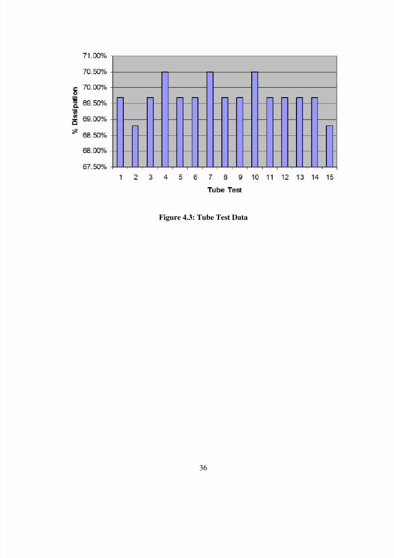
tubes used while Table 4.3 and Figure 4.3 summarize the result of this test; they show that
the system is very accurate with several different kinds of tubes. The average percent
dissipation value is 69.74%, the most deviant value is 68.8% which is 1.2% less than the
ideal value of 70%.
Tube Type Tube Test Set
JJ EL34s 1
Sevtlana EL34s 2
Electro-Harmonix EL34s 3
JJ E34Ls 4
Ruby EL34s 5
Table 4.2: Tube Types used for Testing
The tube sets collected for this test were chosen at random. The 5 different sets are from 4
different companies that are manufactured in different parts of the world. The sets were
ordered from a manufacturer with no request for operating characteristic or sonic qualities.
The randomness in this selection is similar to the randomness of a consumer ordering a
replacement set of tubes for their amplifier, with no specificity to brand, operating
parameters, or quality.

8/14/2019 digital bias
http://slidepdf.com/reader/full/digital-bias 46/62
35
TestNumber
Tube SetPort BOutput
Output BiasVoltage (V)
CathodeCurrent
(A)
ScreenCurrent
(A)
%Dissipation
(W/W)
1 1- test 1 01000000 -35.7 0.093 0.012 69.7%
2 1- test 2 01000000 -35.6 0.092 0.012 68.8%
3 1- test 3 01000000 -35.7 0.093 0.012 69.7%
4 2- test 1 00100100 -38.4 0.094 0.012 70.5%
5 2- test 2 00100100 -38.3 0.093 0.012 69.7%
6 2- test 3 00100100 -38.3 0.093 0.012 69.7%
7 3- test 1 00101000 -38.1 0.094 0.012 70.5%
8 3- test 2 00101000 -38.1 0.093 0.012 69.7%
9 3-test 3 00101000 -38.1 0.093 0.012 69.7%
10 4- test 1 00101100 -37.6 0.094 0.012 70.5%
11 4- test 2 00101100 -37.6 0.093 0.012 69.7%
12 4- test 3 00101100 -37.6 0.093 0.012 69.7%
13 5- test 1 00110100 -36.9 0.093 0.012 69.7%
14 5- test 2 00110100 -36.8 0.093 0.012 69.7%
15 5- test 3 00110100 -36.8 0.092 0.012 68.8%
Table 4.3: Tests
In this table you can see the different output values needed to achieve the same ideal power
tube current value. The microcontroller determined a different binary output value for each
set of tubes, which in turned produced a different output bias voltage. This is significant
because it shows how the same tube type (EL34s) can require a very different bias voltage
for an ideal operating point. In this case as low as -38.3V and as high as -35.6V
8/14/2019 digital bias
http://slidepdf.com/reader/full/digital-bias 47/62
36
Figure 4.3: Tube Test Data

8/14/2019 digital bias
http://slidepdf.com/reader/full/digital-bias 48/62
37
Chapter 5 Conclusions and Recommendations
5.1 Summary and Contributions
This thesis has presented a new non-intrusive digital bias control circuit for tube poweramplifiers. This system automatically finds an ideal biasing point for any tube set used in the
power amplifier. The control system ensures that the bias point does not change over time.
The need for consumer maintenance has been eliminated; saving the consumer from potential
contact with high voltage. This is a practical system that has given the sponsoring company a
major competitive advantage.
This control system is superior to past designs because it uses non-intrusive sampling. This
means that the control does not affect the audio signal quality in any way. This is made
possible by the use of memory via a microcontroller. The microcontroller allows for other
features that have not been possible in past designs, such as tube life warning and monitoring
mechanisms. The final cost of the system is highly dependent on production volume, but
even at low volume can be integrated into an amplifier design for less than $10 in
components.
Overall the system has proven to work reliably and accurately and is ready for
commercialization. It is modular, inexpensive, small, and can easily be integrated into
existing amplifier designs. This system will change the way consumers use tube power
amplifiers. It ensures that power amplifiers are always running at their ideal point without
sacrificing any sonic qualities and eliminates the burden and danger of manual biasing.
5.2 Recommendations for Future Work
The cost and size of this design could be further reduced if a suitable digital potentiometer
were available. Currently there are no digital potentiometers that can withstand a high
negative voltage. As technology advances there may be a digital potentiometer that can
control the high negative bias voltage for power tubes. If this happens there would be no
need for multiple mechanical relays and their associated interfacing circuitry. It would also

8/14/2019 digital bias
http://slidepdf.com/reader/full/digital-bias 49/62
38
reduce the amount of static output ports needed on the microcontroller as the interface would
most likely be serial.
Depending on commercial success, most of the microcontroller’s interfacing circuitry could
be integrated into a single IC. This would greatly reduce the cost and size of the system,
though it is highly dependant on production volume. To ensure a custom IC commercially
viable, tens of thousands need to be manufactured to cover the design overhead and
production costs.

8/14/2019 digital bias
http://slidepdf.com/reader/full/digital-bias 50/62
39
References
[1] Morgan Jones, “Valve Amplifiers”, 2003.[2] Bill Roehr, “A Simple Direct-Coupled Power Mosfet Audio Amplifier Topology
Featuring Bias Stabilization”, November 1982.[3] Joongsik Kih, “Class AB Large Swing CMOS Buffer Amplifier with Controlled Bias
Current”, Dec 1993.[4] John Foster, “Digital Control System for the Thermionic Cathode in an Electron Gun”,
1992.[5] Hammond Inc., “Classic Power Transformers”, December 2009;
http://www.hammondmfg.com/263.htm.[6] Fairchild Semiconductor, “KA78TXX”, September 2009;
http://www.fairchildsemi.com.[7] Hammond Inc.,”Tube Guitar Amplifier Output Transformers”, July 2009;
http://www.hammondmfg.com/guitarLineOT.htm.[8] Sharp USA., “PR31MA11NTZ series datasheet”, September 2009;
http://www.sharpusa.com.[9] Tyco Electronics, “Power PCB Relay RT2”, October 2009;
http://www.tycoelectronics.com/default.aspx.[10] Freescale Semiconductor Inc., “MC68HC908QY4 data sheet”, July 2005;
http://www.freescale.com.[11] Softec Microsystems Inc.,”PK-HC908 user’s manual”, July 2009;
http://www.softecmicro.com/downloads/doc/pk-hc08qy4_manual.pdf .[12] Freescale Semiconductor Inc., “Application Note AN2635”, October 2007;
http://www.freescale.com.

8/14/2019 digital bias
http://slidepdf.com/reader/full/digital-bias 51/62
40
Appendix A
; ---------------------------------------------------------------------
; MAIN.ASM
; ---------------------------------------------------------------------
XDEF Entry, irq_isr, main
; ---------------------------------------------------------------------
; Derivative-specific macros
; ---------------------------------------------------------------------
Include 'MC68HC908QY4.inc'
; ---------------------------------------------------------------------
DEFAULT_ROM SECTION
; ---------------------------------------------------------------------
; Peripheral Initialization
; ---------------------------------------------------------------------
init:
;**********************************************************************
;For commercial use, uncomment parameters for specific tube type
;*********************************************************************
;values are highly dependant on the uP supply voltage, via USB this is
;4.8V not 5V!
;example;;Ideal cathode current = 46.5mA x2 = 93mA
;op-amp gain; 93mA x 33= 3.069
;ADC; (3.069/4.8) x 256= 160
;For EL34s/KT77s at 430V

8/14/2019 digital bias
http://slidepdf.com/reader/full/digital-bias 52/62
41
Vmax: equ 166 ;73%
Vmin: equ 156 ;
danger: equ 200 ; dissipation too high
;For 6L6s at 430V
;Vmax: equ 194 ; 193
;Videal: equ 190 ; 190 Ideal value 49mA cathode 6mA screen
;Vmin: equ 186 ; 187
;danger: equ 220 ; dissipation too high
;**********************************************************************
;Output
StartvalueEL34: equ 30 ; 30 is good start for high gain, 50 for low
;StartvalueEL342: equ %00111110 ; 62 for trans algorithm
bset 0, CONFIG1 ; Disables COP
mov #$49, CONFIG2 ; Enables external oscillator and IRQ/RST pin
mov #$02, OSCSTAT ; Enables external clock generator
lda #0 ;sets very initial output to 0, safety measure
sta PTB
mov #$FF, DDRB ; Configures port B as output mov
#$21, ADSCR ; Enables ADC channel 1
mov #$60, ADICLK ; Bus clock / 8 (0.875Mhz ADC clock)
mov #%00010000, DDRA ;Makes PTA4 output for transparency

8/14/2019 digital bias
http://slidepdf.com/reader/full/digital-bias 53/62
42
rts
; ---------------------------------------------------------------------
; Entry Point
; ---------------------------------------------------------------------
Entry:
main:
rsp ; SP <- 0xFF
cli ; Enables global interrupts
; mov #$00, COPCTL ; COP write
bsr init ; Peripheral initialization
bset 4 , PTA ;activates transparency
jsr delay
;*********************************************************************
;Memory check, erased bits read as 1 and programmed bits read as data
;*********************************************************************
stored_output: equ $FDFA ; FLASH value from last operation
lda #StartvalueEL34 ;default starting point
sta PTB
lda stored_output
cmpa #$FF
beq main_loop ;branch if value is FF, ie FLASH not programmed

8/14/2019 digital bias
http://slidepdf.com/reader/full/digital-bias 54/62
43
lda stored_output
sta PTB
jsr delay
jsr delay
;**********************************************************************
;Main Algorithm
;**********************************************************************
main_loop:
jsr delay
jsr delay
jsr delay
jsr averageADC
cmp #Vmax
bhi less_current ;branch if higher
lda ADCresult ;if ADC less than Vmin, need more current
cmp #Vmin
blo more_current ;branch if lower or same
jsr flash_program
jmp hold ; Forever
more_current:
;increases PTB value which adds less resistance to output ladder, makes
;bias more positive which makes more current flow

8/14/2019 digital bias
http://slidepdf.com/reader/full/digital-bias 55/62
44
lda PTB
add #2
sta PTB ;stores A in port B
jmp main_loop
less_current:
lda PTB
sub #1
sta PTB
jsr delay
jmp main_loop
;**********************************************************************
; Delay Suroutine, 0.599 second delay times 6 = 3.594 seconds
;**********************************************************************
delay:
mov #%00010110, TSC
;internal bus clock/64 = 7Mhz/64= 109.375kHz,resets CLK
delay_loop1:
; mov #0, $FFFF ; COP
brclr 7,TSC ,delay_loop1
mov #%00010110, TSC
delay_loop1b:
; mov #0, $FFFF ; COP

8/14/2019 digital bias
http://slidepdf.com/reader/full/digital-bias 56/62
45
brclr 7,TSC ,delay_loop1b
mov #%00010110, TSC
delay_loop1c:
; mov #0, $FFFF ; COP
brclr 7,TSC ,delay_loop1c
mov #%00010110, TSC
delay_loop1d:
; mov #0, $FFFF ; COP
brclr 7,TSC ,delay_loop1d
mov #%00010110, TSC
delay_loop1e:
; mov #0, $FFFF ; COP
brclr 7,TSC ,delay_loop1e
mov #%00010110, TSC
delay_loop1f:
; mov #0, $FFFF ; COP
brclr 7,TSC ,delay_loop1f
rts
delay_short: ; 0.599 second delay
mov #%00010110, TSC
delay_loop4:
; mov #0, $FFFF ; COP
brclr 7,TSC ,delay_loop4
rts
;**********************************************************************
; Averaging subroutine, returns averaged value on AccA and ADCresult

8/14/2019 digital bias
http://slidepdf.com/reader/full/digital-bias 57/62
46
;**********************************************************************
averageADC:
;mov #0, $FFFF ; COP
ADCresult: equ $00DC ; global variable for ADC result
overflow_count: equ $00D0
lda #0
sta overflow_count ;starts counter at 0
average_sum: equ $00D1
lda #0
sta average_sum
loop_control: equ $00D2
lda #7
sta loop_control
sum_loop:
; mov #0, $FFFF ; COP
lda average_sum
jsr delay_short ;should be short
jsr delay_short
ADCloop1:
brclr 7, ADSCR ,ADCloop1 ; Waits for ADC end of conversion
add ADR
sta average_sum
BCS overflow_add ;branch if carry bit set (overflow)
bra loop_decrement

8/14/2019 digital bias
http://slidepdf.com/reader/full/digital-bias 58/62
47
overflow_add: ;increments overflow_count
lda overflow_count
add #1
sta overflow_count
loop_decrement:
lda loop_control
sub #1
sta loop_control
bpl sum_loop
lda average_sum
lsra ;divide by 8
lsra
lsra
sta average_sum
BCS roundup ;rounds up or skips straight to overflow loop
bra overflow_loop
roundup: ; rounds number up based on lsr division carry out
lda average_sum
add #1
sta average_sum
overflow_loop: ;256/8 = 32
lda average_sum ;adds 32 for each overflow count
add #32
sta average_sum
lda overflow_count
sub #1
sta overflow_count
bpl overflow_loop

8/14/2019 digital bias
http://slidepdf.com/reader/full/digital-bias 59/62
48
lda average_sum ;compensates for initial add
sub #32
sta average_sum
sta ADCresult
cmp #danger ; if input current is too high, branch to protection
bhi protect
rts ;returns with average value in accumulator
;**********************************************************************
;FLASH programming, called from AUX ROM
;**********************************************************************
flash_program:
;programs output value in flash
PRGRNGE: equ $2809 ; PRGRNGE jump address
LADDR: equ $008A
CPUSPD: equ $0089
DATA: equ $008C
mov PTB,DATA
mov #$AA,DATA+1 ;place holder (needed)
mov #$1C,CPUSPD ;fop = 7.0MHz
ldhx #$FDFB ;Load last address to LADDR
sthx LADDR
ldhx #stored_output ;Load beginning address to H:X
jsr PRGRNGE ;Call PRGRNGE routine

8/14/2019 digital bias
http://slidepdf.com/reader/full/digital-bias 60/62
49
lda stored_output
rts
;***********************************************************
;Protection mode for high current
;***********************************************************
protect:
lda #0 ;turns tube off
sta PTB
;***Activate some sort of warning LED or noise (commercial only)
;*********************************************************************
;Holds final state
;*********************************************************************
hold:
lda stored_output ; for debugging
jsr delay
jsr delay
jsr delay
jsr delay
bclr 4, PTA ;activates transparency
bra hold

8/14/2019 digital bias
http://slidepdf.com/reader/full/digital-bias 61/62

8/14/2019 digital bias
http://slidepdf.com/reader/full/digital-bias 62/62