
DIF Digital Imaging Fast - University of Florida · DIF – Digital Imaging ... These will output...
12
University of Florida EEL4924 – Spring 2012 30-Jan-12 Page | 1 Nuhi, Salley DIF – Digital Imaging Fast FPGA Based Image Processing System Members: Ali Nuhi, Everett Salley ABSTRACT The project will implement image processing algorithms in a Field Programmable Gate Array (FPGA). A camera module will output color images that will be fed into the FPGA. The image will be deconstructed into a matrix of pixels that will then go through a series of conversions. Once the image is ready it will go through various image processing algorithms and filters. These will output to a mounted LCD screen for display. Users will be able to select the desired output to the screen as well as be able to change aspects of the image in real time.
Transcript of DIF Digital Imaging Fast - University of Florida · DIF – Digital Imaging ... These will output...

University of Florida EEL4924 – Spring 2012 30-Jan-12 P a g e | 1 Nuhi, Salley
DIF – Digital Imaging Fast
FPGA Based Image Processing System
Members: Ali Nuhi, Everett Salley
ABSTRACT The project will implement image processing algorithms in a Field Programmable Gate Array
(FPGA). A camera module will output color images that will be fed into the FPGA. The image
will be deconstructed into a matrix of pixels that will then go through a series of conversions.
Once the image is ready it will go through various image processing algorithms and filters.
These will output to a mounted LCD screen for display. Users will be able to select the desired
output to the screen as well as be able to change aspects of the image in real time.

University of Florida EEL4924 – Spring 2012 30-Jan-12 P a g e | 2 Nuhi, Salley
Contents ABSTRACT ...................................................................................................................................................... 1
INTRODUCTION ............................................................................................................................................. 3
TECHNICAL OBJECTIVES ................................................................................................................................ 4
IMAGE PROCESSING ...................................................................................................................................... 5
HARDWARE DESIGN ...................................................................................................................................... 7
SOFTWARE DESIGN ....................................................................................................................................... 8
COST OBJECTIVES ........................................................................................................................................ 11
DIVISION OFLABOR ..................................................................................................................................... 11
GANTT CHART ............................................................................................................................................. 11
List of Tables BILL OF MATERIALS ……………………………………………………………………………………………………………………………….11 DIVISION OF LABOR ………………………………………………………………………………………………………………………………11
Figures BLOCK DIAGRAM …………………………………………………………………………………………………………………………………..4 CONVOLUTION ………………………………………………………………………………………………………………………………………5 SOBEL …………………………………………………………………………………………………………………………………………………...5 PREWITT…………………… ………………………………………………………………………………………………………………………….5 CROSS …………………………………………………………………………………………………………………………………………………..6 MEDIAN ………………………………………………………………………………………………………………………………………………..6 CAMERA ……………………………………………………………………………………………………………………………………………….7 LCD ……………………………………………………………………………………………………………………………………………………….7 MICRO CONTROLLER .……..…………………………………………………………………………………………………………………….8 MEMORY CONTROLLER ………………………………………………………………………………………………………………………..9 WINDOW GENERATOR …………………………………………………………………………………………………………………………10 PROCESSING BLOCK ……………………………………………………………………………………………………………………………..10 GANNT CHART ……………………………………………………………………………………………………………………………………..12

University of Florida EEL4924 – Spring 2012 30-Jan-12 P a g e | 3 Nuhi, Salley
INTRODUCTION As higher definition video becomes more common, processing power must increase. Most
current systems utilize a high speed Digital Signal Processor to achieve goals. However, as video
quality increases the only option is to increase the clock frequency, leading to more
complicated designs that consume larger amounts of power. One possible way of bypassing
this problem is to implement image processing algorithms in hardware. This has the distinct
advantage of allowing a manageable clock frequency to be used and much less overhead.
Current systems on the market that utilize an FPGA for image processing are digital video
surveillance units.
Much of the theory in digital signal processing is covered throughout the electrical engineering
coursework but there is very little hands on experience in DSP hardware design. FPGA
development boards exist that are capable of implementing image processing algorithms, but
affordable boards often do not include any sort of camera or LCD screen. Our project aims to
offer a means to implement image processing algorithms with a single, low cost board.
Our system will utilize an embedded camera and FPGA to create an image processing unit. The
system will be able to create different image transformations, such as edge detection. The
FPGA allows for easier ‘plugging in’ of algorithm modules as long as the input and output
specifications are followed. We would like the user to be able to choose the type of output
such as straight through video, black and white, and edge detection using, for example, Sobel
edge detection.

University of Florida EEL4924 – Spring 2012 30-Jan-12 P a g e | 4 Nuhi, Salley
Figure 1: Block Diagram
TECHNICAL OBJECTIVES The overall goal of our project is to implement image processing algorithms on video such that
the results can be seen in real-time.
The camera module will be responsible for providing a constant stream of RGB pixel data. If possible, we would like to interface it directly to the FPGA.
The primary function of the FPGA will be to implement the various image processing algorithms. Additionally, the FPGA will also drive our LCD screen, read and write to external memory, control the camera module, and handle I/O from the user.
The ability to easily switch between the different kinds of output for the screen (true video, grayscale, edge detection, etc...)
The screen and camera will operate at different frequencies and frame rates, therefore it is important to establish a reliable frame buffer with external memory. Additionally, the clock rate differences will introduce clock domain crossing issues which must be resolved.
A four layer PCB will likely be necessary in order to adequately manage the various power supplies in the system.
Real-time image processing

University of Florida EEL4924 – Spring 2012 30-Jan-12 P a g e | 5 Nuhi, Salley
IMAGE PROCESSING One of the most widely used operations in the field of image processing is the two dimensional
convolution. A high level view of the algorithm contains a window of NxN pixels that is convolved with
an NxN operator that produces the desired effect of the filter. The operator kernel slides across the
image N rows at a time until the entire image is done. At each window N2 multiply accumulate
operations must be calculated before the next window of pixels is shifted in.
Figure 2: Convolution
Sobel Operator: The Sobel operator works by taking the derivative of the image in the x and y direction
and then uses this information to calculate the magnitude of the gradient.
Figure 3: Sobel
Prewitt Operator: The Prewitt operator uses a different kernel than Sobel but it essentially performs the
same task.
Figure 4: Prewitt

University of Florida EEL4924 – Spring 2012 30-Jan-12 P a g e | 6 Nuhi, Salley
Cross Operator: The cross operator approximates the gradient through discrete differentiation. The
kernel itself is only 2x2 however, so it is more computationally efficient.
Figure 5: Cross
Laplace Operator: The Laplace operator also finds the gradient of the image, but it does so without the
need to calculate the magnitude of two vectors. The tradeoff is that works using the 2nd derivative and
therefore is more susceptible to noise. The Laplace operator is not set and has many different versions
depending on the desired standard deviation.
Median Filter: The median filter is slightly different because it performs a series of comparisons on the
window to find the median value instead of a convolution.
Figure 6: Median

University of Florida EEL4924 – Spring 2012 30-Jan-12 P a g e | 7 Nuhi, Salley
HARDWARE DESIGN Camera:
The camera used is a Toshiba TCM8230MD CMOS camera. This unit was chosen because it meets VGA
output formatting and was relatively easy to use. It is controlled via I2C commands that we sent to it
with an MSP430F2272. The camera is driven at 25MHz and provides a 640x480 pixel image at 30fps in
5:6:5 RGB format that we then cut down to fit our LCD screen.
Figure 7: Camera
Screen:
The screen used is a Sharp LQ043T3DX02 Sony PSP replacement screen. The screen requires 24bit data
per pixel to run. The final output image size was dependent on the screen size which is 480x272 pixels.
The screen runs 9MHz which gave us a hard deadline for when pixels need to be ready.
Figure 8: LCD Screen

University of Florida EEL4924 – Spring 2012 30-Jan-12 P a g e | 8 Nuhi, Salley
Microcontroller:
A TI MSP430F2272 was used to send commands to the camera as well as an provide analog to digital
conversion for the potentiometer that provides user interaction
Figure 9: Microcontroller
Memory:
A Cypress CY7C1357C Synchronous SRAM was used as an external frame buffer. The external memory
was required because there was not enough memory available on the FPGA to buffer an entire frame. It
is capable of running at 133MHz so some high speed board design issues needed to be considered such
as equal length traces.
FPGA:
We used an Altera Cyclone 3 FPGA (EP3C16E240C8N) to perform the majority of the interfacing and
processing/computation. The 240 pin package was the smallest package we could find that wasn't BGA
and had enough I/O pins (160) to interface with all of our components. The FPGA includes over 15,000
logic elements, 500,000+ bits of memory, 4 dedicated PLLs, and 112 dedicated hardware multipliers.
SOFTWARE DESIGN The majority of software design for this project was done using VHSIC Hardware Description Language
or VHDL. Since an Altera Cyclone III was used the QUARTUS II 11.1sp2 Design Suite was used for
compilation and programming. Further, ModelSim-Altera 10.0c was used to test VHDL designs during
the prototyping process.
The overall goal of the design was to create a modular system that would allow for easy changing of
code for future iterations. This was done by creating a defined camera and screen interface that could
be used as any I/O would. Once these were defined then anything could be plugged in between them as
long as timing requirement s are met.
Camera Interface:
Since the camera outputs 16bit pixels 8bits at a time that is synchronized with a clock we created an
interface that would wait until a full pixel was ready and output a pixel at a time. This interface also
kept track of vertical and horizontal syncs done by the camera that signify an end to a frame and a line.
Memory Controller:
University of Florida EEL4924 – Spring 2012 30-Jan-12 P a g e | 9 Nuhi, Salley
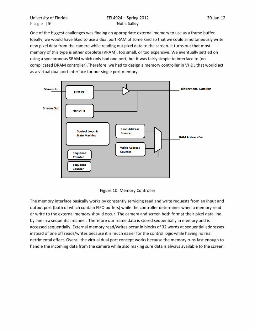
One of the biggest challenges was finding an appropriate external memory to use as a frame buffer.
Ideally, we would have liked to use a dual port RAM of some kind so that we could simultaneously write
new pixel data from the camera while reading out pixel data to the screen. It turns out that most
memory of this type is either obsolete (VRAM), too small, or too expensive. We eventually settled on
using a synchronous SRAM which only had one port, but it was fairly simple to interface to (no
complicated DRAM controller).Therefore, we had to design a memory controller in VHDL that would act
as a virtual dual port interface for our single port memory.
Figure 10: Memory Controller
The memory interface basically works by constantly servicing read and write requests from an input and
output port (both of which contain FIFO buffers) while the controller determines when a memory read
or write to the external memory should occur. The camera and screen both format their pixel data line
by line in a sequential manner. Therefore our frame data is stored sequentially in memory and is
accessed sequentially. External memory read/writes occur in blocks of 32 words at sequential addresses
instead of one off reads/writes because it is much easier for the control logic while having no real
detrimental effect. Overall the virtual dual port concept works because the memory runs fast enough to
handle the incoming data from the camera while also making sure data is always available to the screen.

University of Florida EEL4924 – Spring 2012 30-Jan-12 P a g e | 10 Nuhi, Salley
Processing Data Path:
The processing data path reads from the external memory and writes a line buffer that can hold 3 full
rows of the image. This line buffer feeds into a window generator that creates valid windows for the
convolution module.
Figure 11: Window Generator
The processing block contains various filters that are all done in parallel to achieve maximum
performance. This was an extremely important aspect of the data paths design in that we wanted to
have the output of each filter ready at the same time. This allows us to be able to actively choose which
output to be displayed to the screen with no delay between modes.
Figure 12: Processing Block
Screen Controller:
The screen controller was written to handle the overall delay of the system as well as the generation of
synchronizing pulses. The other main job was to make sure a pixel was ready to be written when the
screen requested it.

University of Florida EEL4924 – Spring 2012 30-Jan-12 P a g e | 11 Nuhi, Salley
COST OBJECTIVES
Table 1: Bill of Materials
DIVISION OF LABOR
Ali Nuhi Everett Salley
Camera Module 70% 30% Screen Module 10% 90% Microcontroller 75% 25%
PCB 40% 60% VHDL Design 50% 50%
Table 2: Division of Labor
Component Price
Cyclone 3 FPGA $30 Camera $10 LCD Screen $20 SSRAM $10 4 Layer PCB $66 Misc Components $10-$20 Total ~$160

University of Florida EEL4924 – Spring 2012 30-Jan-12 P a g e | 12 Nuhi, Salley
GANTT CHART Spring 2012 Gannt Chart
Figure 13: Gannt Chart
0 1 2 3 4 5 6 7 8 9 10 11 12 13 14 15 16
Introduction (team)
Ideas/Project Proposal
System design
Research/Simulations
Board design/Testing/Ordering
Debug
Demo (team)
Available Weeks in Spring 2012
PlannedExtension Down time


![Strictly Private and Confidential [DRAFT] Digital …investor.digital-tif.com/misc/PRESN/20160516-dif... · 2016. 6. 20. · Digital Telecommunications Infrastructure Fund (“DIF”)](https://static.fdocuments.us/doc/165x107/5fcc3dfead6f7706332233f7/strictly-private-and-confidential-draft-digital-2016-6-20-digital-telecommunications.jpg)

![Strictly Private and Confidential [DRAFT] Digital ...investor.digital-tif.com/misc/PRESN/20170407-dif-investor-apr17.pdf · Digital Telecommunications Infrastructure Fund (“DIF”)](https://static.fdocuments.us/doc/165x107/5f054fdd7e708231d41256ea/strictly-private-and-confidential-draft-digital-digital-telecommunications.jpg)


