High-order Implicit relaxation schemes for hyperbolic models
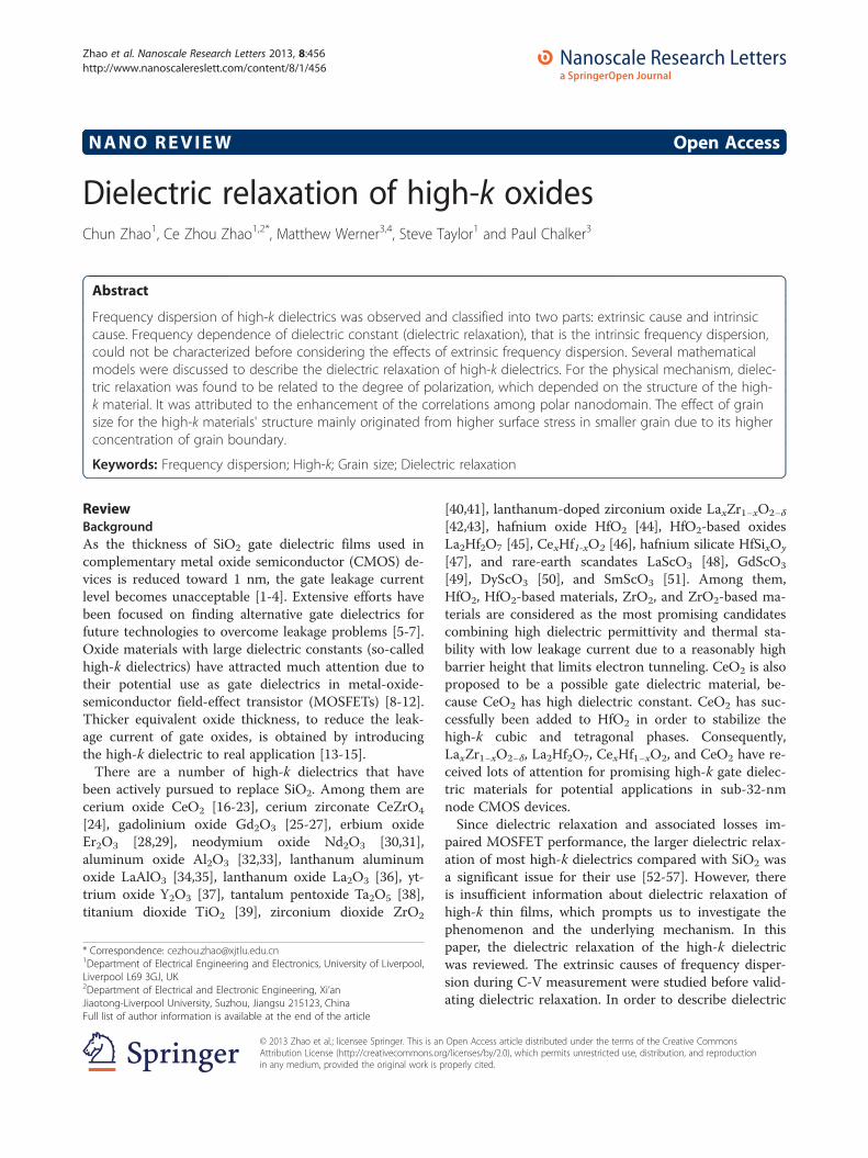
Zhao et al. Nanoscale Research Letters 2013, 8:456http://www.nanoscalereslett.com/content/8/1/456
NANO REVIEW Open Access
Dielectric relaxation of high-k oxidesChun Zhao1, Ce Zhou Zhao1,2*, Matthew Werner3,4, Steve Taylor1 and Paul Chalker3
Abstract
Frequency dispersion of high-k dielectrics was observed and classified into two parts: extrinsic cause and intrinsiccause. Frequency dependence of dielectric constant (dielectric relaxation), that is the intrinsic frequency dispersion,could not be characterized before considering the effects of extrinsic frequency dispersion. Several mathematicalmodels were discussed to describe the dielectric relaxation of high-k dielectrics. For the physical mechanism, dielec-tric relaxation was found to be related to the degree of polarization, which depended on the structure of the high-k material. It was attributed to the enhancement of the correlations among polar nanodomain. The effect of grainsize for the high-k materials' structure mainly originated from higher surface stress in smaller grain due to its higherconcentration of grain boundary.
Keywords: Frequency dispersion; High-k; Grain size; Dielectric relaxation
ReviewBackgroundAs the thickness of SiO2 gate dielectric films used incomplementary metal oxide semiconductor (CMOS) de-vices is reduced toward 1 nm, the gate leakage currentlevel becomes unacceptable [1-4]. Extensive efforts havebeen focused on finding alternative gate dielectrics forfuture technologies to overcome leakage problems [5-7].Oxide materials with large dielectric constants (so-calledhigh-k dielectrics) have attracted much attention due totheir potential use as gate dielectrics in metal-oxide-semiconductor field-effect transistor (MOSFETs) [8-12].Thicker equivalent oxide thickness, to reduce the leak-age current of gate oxides, is obtained by introducingthe high-k dielectric to real application [13-15].There are a number of high-k dielectrics that have
been actively pursued to replace SiO2. Among them arecerium oxide CeO2 [16-23], cerium zirconate CeZrO4
[24], gadolinium oxide Gd2O3 [25-27], erbium oxideEr2O3 [28,29], neodymium oxide Nd2O3 [30,31],aluminum oxide Al2O3 [32,33], lanthanum aluminumoxide LaAlO3 [34,35], lanthanum oxide La2O3 [36], yt-trium oxide Y2O3 [37], tantalum pentoxide Ta2O5 [38],titanium dioxide TiO2 [39], zirconium dioxide ZrO2
* Correspondence: [email protected] of Electrical Engineering and Electronics, University of Liverpool,Liverpool L69 3GJ, UK2Department of Electrical and Electronic Engineering, Xi’anJiaotong-Liverpool University, Suzhou, Jiangsu 215123, ChinaFull list of author information is available at the end of the article
© 2013 Zhao et al.; licensee Springer. This is anAttribution License (http://creativecommons.orin any medium, provided the original work is p
[40,41], lanthanum-doped zirconium oxide LaxZr1−xO2−δ
[42,43], hafnium oxide HfO2 [44], HfO2-based oxidesLa2Hf2O7 [45], CexHf1-xO2 [46], hafnium silicate HfSixOy
[47], and rare-earth scandates LaScO3 [48], GdScO3
[49], DyScO3 [50], and SmScO3 [51]. Among them,HfO2, HfO2-based materials, ZrO2, and ZrO2-based ma-terials are considered as the most promising candidatescombining high dielectric permittivity and thermal sta-bility with low leakage current due to a reasonably highbarrier height that limits electron tunneling. CeO2 is alsoproposed to be a possible gate dielectric material, be-cause CeO2 has high dielectric constant. CeO2 has suc-cessfully been added to HfO2 in order to stabilize thehigh-k cubic and tetragonal phases. Consequently,LaxZr1−xO2−δ, La2Hf2O7, CexHf1−xO2, and CeO2 have re-ceived lots of attention for promising high-k gate dielec-tric materials for potential applications in sub-32-nmnode CMOS devices.Since dielectric relaxation and associated losses im-
paired MOSFET performance, the larger dielectric relax-ation of most high-k dielectrics compared with SiO2 wasa significant issue for their use [52-57]. However, thereis insufficient information about dielectric relaxation ofhigh-k thin films, which prompts us to investigate thephenomenon and the underlying mechanism. In thispaper, the dielectric relaxation of the high-k dielectricwas reviewed. The extrinsic causes of frequency disper-sion during C-V measurement were studied before valid-ating dielectric relaxation. In order to describe dielectric
Open Access article distributed under the terms of the Creative Commonsg/licenses/by/2.0), which permits unrestricted use, distribution, and reproductionroperly cited.

Zhao et al. Nanoscale Research Letters 2013, 8:456 Page 2 of 12http://www.nanoscalereslett.com/content/8/1/456
relaxation, many mathematic models were proposed.After mathematical models were finalized for fitting ex-perimental data, physical mechanisms of dielectric relax-ation were under investigation. Dielectric relaxationbehaviors observed in the high-k dielectrics were partlydue to the level of stress in the crystalline grains, de-pending on the grain size, analogous to the behavior offerroelectric ceramics. As surface stress changes, glass-like transition temperature varied considerably. Dielec-tric relaxation appears to be a common feature inferroelectrics associated with non-negligible ionicconductivity.
MethodsSample preparationHfO2, ZrO2, and LaAlO3 thin films were deposited onn-type Si(100) substrates using liquid injection metal or-ganic chemical vapor deposition (MOCVD) or atomiclayer deposition (ALD), carried out on a modified Aix-tron AIX 200FE AVD reactor (Herzogenrath, Germany)fitted with the “Trijet”™ liquid injector system. Duringthe MOCVD experiments, oxygen was introduced at theinlet of the reactor. For the ALD experiments, the oxy-gen was replaced by water vapor, which was controlledby a pneumatic valve. The substrate was rotatedthroughout all experiments for good uniformity. Augerelectron spectroscopy (AES) results suggested they arestoichiometric films. All the high-k dielectric layers con-sidered were 16 nm in thickness.LaxZr1−xO2−δ thin films were deposited onto n-type Si
(100) wafers by the same modified Aixtron AIX 200FEAVD reactor liquid injection ALD at 300°C. Both Zr andLa sources were Cp-based precursors ([(MeCp)2ZrMe(OMe)] and [(iPrCp)3La]). The La concentration wasvaried in different films. Particular attention has beengiven to the results from films with a La concentrationof x = 0.09 (55 nm) and x = 0.35 (35 nm) but results arealso included from films with a concentration of x = 0.22(50 nm) and x = 0, i.e., un-doped ZrO2 (35 nm). Post de-position annealing was performed at 900°C in a pure N2
ambient for 15 min. To form MOS capacitors (Au/LaxZr1−xO2/IL/n-Si, where IL stands for interfaciallayer), metal (Au) gate electrodes with an effective con-tact area of 4.9 × 10⁻⁴ cm2 were evaporated onto thesamples. The backsides of the Si samples were cleanedwith a buffered HF solution and subsequently a 200-nm-thick film of Al was deposited by thermal evaporation toform an ohmic back contact.La2Hf2O7 thin films were deposited on n-type Si(100)
substrates by the same liquid injection ALD at 300°C.Both Hf and La sources are Cp-based precursors([(MeCp)2HfMe(OMe)] and [(iPrCp)3La]). The compos-ition of the La-doped HfO2 thin films was estimated to
be La2Hf2O7. Selected thin films were subjected to 900°Cpost-deposition annealing (PDA) in N2 for 15 min.Amorphous CexHf1−xO2 thin films (x = 0.1) were de-
posited on n-type Si(100) substrates using the same li-quid injection ALD. The doping level was varied up to aconcentration level of 63%, i.e., x = 0.63. The interfaciallayer between high-k thin film and silicon substrate is ap-proximately 1-nm native SiO2. Samples were then annealedat 900°C for 15 min in an N2 ambient to crystallize thethin films.CeO2 thin films used the same liquid injection ALD
for deposition. The precursor was a 0.05 M solution of[Ce(mmp)4] in toluene and a source of oxygen was de-ionized water. ALD procedures were run at substratetemperatures of 150, 200, 250, 300, and 350°C, respect-ively. The evaporator temperature was 100°C and reactorpressure was 1 mbar. CeO2 films were grown on n-Si(100) wafers. Argon carrier gas flow was performed with100 cm3 · min−1. The flow of [Ce(mmp)4]/purge/H2O/purge was 2/2/0.5/3.5 s and the number of growth cycleswas 300, which is important in order to achieve highreproducibility of film growth and precise control offilm thickness by the number of deposition cycles.The thicknesses for the samples are within 56 nm to98 nm. Post deposition annealing (PDA) was operatedon the 250°C as-deposited samples in vacuum at 800°Cfor 15 min.
Material characterizationThe physical properties of the high-k thin films werestudied using X-ray diffraction (XRD) and cross-sectional transmission electron microscopy (XTEM).Electrical properties of the films were obtained bycapacitance-voltage (C-V) and capacitance-frequency(C-f ).XRD were operated using a Rigaku Miniflex diffractom-
eter (Beijing, China) with CuKα radiation (0.154051 nm,40 kV, 50 mA) spanning a 2θ range of 20° to 50° at a scanrate of 0.01°/min.Atomic force microscopy (AFM) was used to investi-
gate variations in surface morphology of these films, andwas carried out using a Digital Instruments NanoscopeIII, in contact mode.AES was used to determine the atomic composition of
the thin films, which was carried out using a Varianscanning Auger spectrometer (Palo Alto, CA, USA). Theatomic compositions are from the bulk of the thin film,free from surface contamination, and were obtained bycombining AES with sequential argon ion bombardmentuntil comparable compositions were obtained for con-secutive data points.XTEM was used to obtain the film thickness and in-
formation about the crystal grain size. A JEOL 3010 or a
Zhao et al. Nanoscale Research Letters 2013, 8:456 Page 3 of 12http://www.nanoscalereslett.com/content/8/1/456
JEOL 2000FX (Akishima-shi, Japan) operated at 300 and200 keV, respectively, was used.C-V measurements were implemented using an Agi-
lent E4980A precision LCR meter (Santa Clara, CA,USA). C-V measurements were performed in parallelmode, from strong inversion toward strong accumula-tion (and vice versa), at frequencies ranging from 20 Hzto 2 MHz. C-f measurements were carried out in astrong accumulation region.
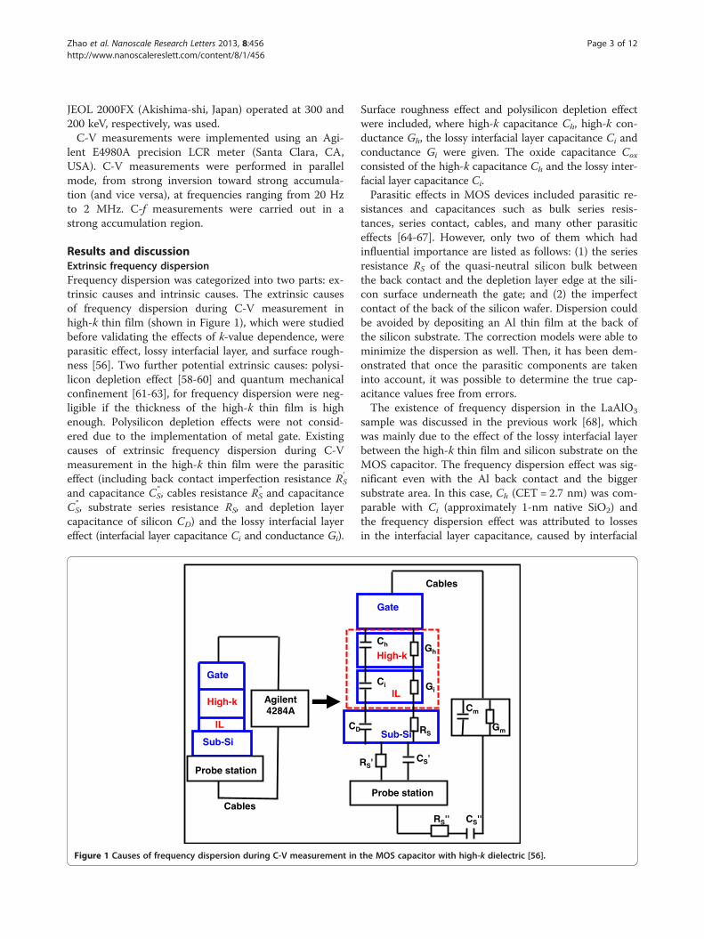
Results and discussionExtrinsic frequency dispersionFrequency dispersion was categorized into two parts: ex-trinsic causes and intrinsic causes. The extrinsic causesof frequency dispersion during C-V measurement inhigh-k thin film (shown in Figure 1), which were studiedbefore validating the effects of k-value dependence, wereparasitic effect, lossy interfacial layer, and surface rough-ness [56]. Two further potential extrinsic causes: polysi-licon depletion effect [58-60] and quantum mechanicalconfinement [61-63], for frequency dispersion were neg-ligible if the thickness of the high-k thin film is highenough. Polysilicon depletion effects were not consid-ered due to the implementation of metal gate. Existingcauses of extrinsic frequency dispersion during C-Vmeasurement in the high-k thin film were the parasiticeffect (including back contact imperfection resistance RS
’
and capacitance CS” , cables resistance RS
” and capacitanceCS” , substrate series resistance RS, and depletion layer
capacitance of silicon CD) and the lossy interfacial layereffect (interfacial layer capacitance Ci and conductance Gi).
IL
Sub-Si
Gate
High-k Agilent 4284A
Cables
CD
Probe station
Figure 1 Causes of frequency dispersion during C-V measurement in
Surface roughness effect and polysilicon depletion effectwere included, where high-k capacitance Ch, high-k con-ductance Gh, the lossy interfacial layer capacitance Ci andconductance Gi were given. The oxide capacitance Cox
consisted of the high-k capacitance Ch and the lossy inter-facial layer capacitance Ci.Parasitic effects in MOS devices included parasitic re-
sistances and capacitances such as bulk series resis-tances, series contact, cables, and many other parasiticeffects [64-67]. However, only two of them which hadinfluential importance are listed as follows: (1) the seriesresistance RS of the quasi-neutral silicon bulk betweenthe back contact and the depletion layer edge at the sili-con surface underneath the gate; and (2) the imperfectcontact of the back of the silicon wafer. Dispersion couldbe avoided by depositing an Al thin film at the back ofthe silicon substrate. The correction models were able tominimize the dispersion as well. Then, it has been dem-onstrated that once the parasitic components are takeninto account, it was possible to determine the true cap-acitance values free from errors.The existence of frequency dispersion in the LaAlO3
sample was discussed in the previous work [68], whichwas mainly due to the effect of the lossy interfacial layerbetween the high-k thin film and silicon substrate on theMOS capacitor. The frequency dispersion effect was sig-nificant even with the Al back contact and the biggersubstrate area. In this case, Ch (CET = 2.7 nm) was com-parable with Ci (approximately 1-nm native SiO2) andthe frequency dispersion effect was attributed to lossesin the interfacial layer capacitance, caused by interfacial
Gate
High-k
IL
Sub-Si
Probe station
C-V
RS''
CS'RS'
RS
CS''
Cables
Ci
Ch Gh
Gi
Cm
Gm
the MOS capacitor with high-k dielectric [56].
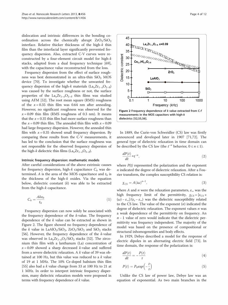
Figure 2 Frequency dependence of k value extracted from C-fmeasurements in the MOS capacitors with high-kdielectrics [52,55,56].
Zhao et al. Nanoscale Research Letters 2013, 8:456 Page 4 of 12http://www.nanoscalereslett.com/content/8/1/456
dislocation and intrinsic differences in the bonding co-ordination across the chemically abrupt ZrO2/SiO2
interface. Relative thicker thickness of the high-k thinfilm than the interfacial layer significantly prevented fre-quency dispersion. Also, extracted C-V curves were re-constructed by a four-element circuit model for high-kstacks, adapted from a dual frequency technique [69],with the capacitance value reconstructed from the loss.Frequency dispersion from the effect of surface rough-
ness was best demonstrated in an ultra-thin SiO2 MOSdevice [70]. To investigate whether the unwanted fre-quency dispersion of the high-k materials (LaxZr1−xO2−δ)was caused by the surface roughness or not, the surfaceproperties of the LaxZr1−xO2−δ thin films was studiedusing AFM [52]. The root mean square (RMS) roughnessof the x = 0.35 thin film was 0.64 nm after annealing.However, no significant roughness was observed for thex = 0.09 thin film (RMS roughness of 0.3 nm). It meansthat the x = 0.35 thin film had more surface roughness thanthe x = 0.09 thin film. The annealed thin film with x = 0.09had large frequency dispersion. However, the annealed thinfilm with x = 0.35 showed small frequency dispersion. Bycomparing these results from the C-V measurements, ithas led to the conclusion that the surface roughness wasnot responsible for the observed frequency dispersion ofthe high-k dielectric thin films (LaxZr1−xO2−δ).
Intrinsic frequency dispersion: mathematic modelsAfter careful considerations of the above extrinsic causesfor frequency dispersion, high-k capacitance Ch was de-termined. A is the area of the MOS capacitance and th isthe thickness of the high-k oxides. Via the equationbelow, dielectric constant (k) was able to be extractedfrom the high-k capacitance.
Ch ¼ Akε0th
ð1Þ
Frequency dispersion can now solely be associated withthe frequency dependence of the k-value. The frequencydependence of the k value can be extracted as shown inFigure 2. The figure showed no frequency dependence ofthe k value in LaAlO3/SiO2, ZrO2/SiO2 and SiO2 stacks[56]. However, the frequency dependence of the k-valuewas observed in LaxZr1–xO2/SiO2 stacks [52]. The zirco-nium thin film with a lanthanum (La) concentration ofx = 0.09 showed a sharp decreased k-value and sufferedfrom a severe dielectric relaxation. A k value of 39 was ob-tained at 100 Hz, but this value was reduced to a k valueof 19 at 1 MHz. The 10% Ce-doped hafnium thin film[55] also had a k value change from 33 at 100 Hz to 21 at1 MHz. In order to interpret intrinsic frequency disper-sion, many dielectric relaxation models were proposed interms with frequency dependence of k value.
In 1889, the Curie-von Schweidler (CS) law was firstlyannounced and developed later in 1907 [71,72]. Thegeneral type of dielectric relaxation in time domain canbe described by the CS law (the t−n behavior, 0 ≤ n ≤ 1).
dP tð Þdt
∝t−n; ð2Þ
where P(t) represented the polarization and the exponentn indicated the degree of dielectric relaxation. After a Fou-rier transform, the complex susceptibility CS relation is:
χCS ¼ A iωð Þn−1; ð3Þwhere A and n were the relaxation parameters, ε∞ was thehigh frequency limit of the permittivity, χCS = [εCS ×(ω) − ε∞]/(εs − ε∞) was the dielectric susceptibility relatedto the CS law. The value of the exponent (n) indicated thedegree of dielectric relaxation. The exponent values n wasa weak dependence of the permittivity on frequency. Ann − 1 value of zero would indicate that the dielectric per-mittivity was frequency independent. The majority of themodel was based on the presence of compositional orstructural inhomogeneities and body effects.In 1929, Debye described a model for the response of
electric dipoles in an alternating electric field [73]. Intime domain, the response of the polarization is:
dP tð Þdt
¼ −P tð Þτ
ð4Þ
P tð Þ ¼ P0exp −tτ
� �ð5Þ
Unlike the CS law of power law, Debye law was anequation of exponential. As two main branches in the
Zhao et al. Nanoscale Research Letters 2013, 8:456 Page 5 of 12http://www.nanoscalereslett.com/content/8/1/456
development of dielectric relaxation modeling, the CSand Debye are the origins along the evolution beyonddoubt. The Debye model led to a description for thecomplex dielectric constant ε*. An empirical expression,which originated from the Debye law, was proposed byKohlrausch, Williams, and Watts, which is a stretchedexponential function, to be referred to later as theKohlrausch-Williams-Watts (KWW) function widelyused to describe the relaxation behavior of glass-forming liquids and other complex systems [74-76]. Theequivalent of the dielectric response function in timedomain is
P tð Þ ¼ P0exp −tτ
� �βKWW� �
ð6Þ
After a Fourier transform, the Debye equation in thefrequency domain and its real and imaginary parts are
ε� ωð Þ ¼ ε∞ þ εs−ε∞1þ iωτð Þ ð7Þ
ε0ωð Þ ¼ ε∞ þ εs−ε∞
1þ ω2τ2ð8Þ
ε00ωð Þ εs−ε∞ð Þωτ
1þ ω2τ2ð9Þ
where τ was called the relaxation time which was a func-tion of temperature and it was independent of the timeangular frequency ω = 2πf. εs was also defined as thezero-frequency limit of the real part, ε’, of the complexpermittivity. ε∞ was the dielectric constant at ultra-highfrequency. Finally, ε’ was the k value.The Debye theory assumed that the molecules were
spherical in shape and dipoles were independent in theirresponse to the alternating field with only one relaxationtime. Generally, the Debye theory of dielectric relaxationwas utilized for particular types of polar gases and dilutesolutions of polar liquids and polar solids. However, thedipoles for a majority of materials were more likely to beinteractive and dependent in their response to the alter-nating field. Therefore, very few materials completelyagreed with the Debye equation which had only one re-laxation time.Since the Debye expression cannot properly predict
the behavior of some liquids and solids such as chlori-nated diphenyl at −25°C and cyclohexanone at −70°C, in1941, Cole K.S. and Cole R.H. proposed an improved
Debye equation, known as the Cole-Cole equation, to in-terpret data observed on various dielectrics [77]. TheCole-Cole equation can be represented by ε*(ω):
ε� ωð Þ ¼ ε∞ þ εs−ε∞1þ iωτð Þ1−α ; ð10Þ
where τ was the relaxation time and α was a constantfor a given material, having a value 0 ≤ α ≤ 1. α = 0 forDebye relaxation. The real and imaginary parts of theCole-Cole equation are
ε0ωð Þ ¼ ε∞
þ εs−ε∞ð Þ 1þ ωτð Þ1−α sin 12 απ� �
1þ 2 ωτð Þ1−α sin 12 απ� �þ ωτð Þ2 1−αð Þ
ð11Þ
ε00ωð Þ ¼ εs−ε∞ð Þ 1þ ωτð Þ1−α cos 1
2 απ� �
1þ 2 ωτð Þ1−α sin 12 απ� �þ ωτð Þ2 1−αð Þ
ð12Þ
Ten years later, in 1951, Davidson et al. proposed thefollowing expression (Cole-Davidson equation) to inter-pret data observed on propylene glycol and glycerol[78-81] based on the Debye expression:
ε� ωð Þ ¼ ε∞ þ εs−ε∞1þ iωτð Þβ ; ð13Þ
where τ was the relaxation time and β was a constantfor a given material. 0 ≤ β ≤ 1 which controlled the widthof the distribution and β = 1 for Debye relaxation. Thesmaller the value of β, the larger the distribution of re-laxation times. The real and imaginary parts of the Cole-Davidson equation are given by
ε0ωð Þ ¼ ε∞ þ εs−ε∞ð Þ cosφð Þβ cosβφ ð14Þ
ε00ωð Þ ¼ εs−ε∞ð Þ cosφð Þβ sinβφ ð15Þ
φ ¼ tan−1 ωτð Þ ð16Þ
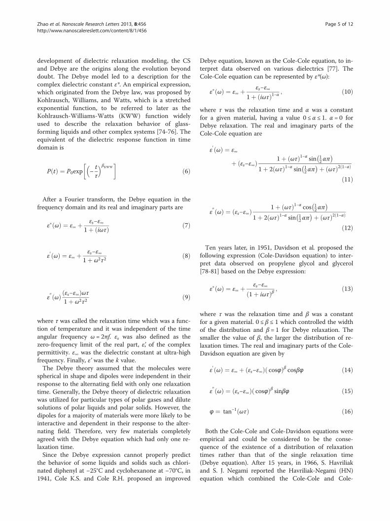
Both the Cole-Cole and Cole-Davidson equations wereempirical and could be considered to be the conse-quence of the existence of a distribution of relaxationtimes rather than that of the single relaxation time(Debye equation). After 15 years, in 1966, S. Havriliakand S. J. Negami reported the Havriliak-Negami (HN)equation which combined the Cole-Cole and Cole-
Figure 3 Evolution map for Debye, Cole-Cole, Cole-Davidson,and HN model.
Zhao et al. Nanoscale Research Letters 2013, 8:456 Page 6 of 12http://www.nanoscalereslett.com/content/8/1/456
Davidson equations for 21 polymers [82-84]. The HNequation is
ε� ωð Þ ¼ ε∞ þ εs−ε∞
1þ iωτð Þ1−α� β ð17Þ
The real and imaginary parts of the HN equation aregiven by
ε0ωð Þ ¼ ε∞
þ εs−ε∞ð Þ cos βΦð Þ1þ 2 ωτð Þ1−α sin πα
2
� �þ ωτð Þ2 1−αð Þh iβ
2
ð18Þ
ε00ωð Þ ¼ εs−ε∞ð Þ sin βΦð Þ
1þ 2 ωτð Þ1−α sin πα2
� �þ ωτð Þ2 1−αð Þh iβ
2
ð19Þ
Φ ¼ tan−1ωτð Þ1−α cos 12πα
1þ ωτð Þ1−α sin 12πα
ð20Þ
where α and β were the two adjustable fitting parame-ters. α was related to the width of the loss peak and βcontrolled the asymmetry of the loss peak. In this model,parameters α and β could both vary between 0 and 1.The Debye dielectric relaxation model with a single re-laxation time from α = 0 and β = 1, the Cole-Cole modelwith symmetric distribution of relaxation times followedfor β = 1 and 0 ≤ α ≤ 1, and the Cole-Davidson modelwith an asymmetric distribution of relaxation times fol-lows for α = 0 and 0 ≤ β ≤ 1. The HN equation had twodistribution parameters α and β but Cole-Cole andCole-Davidson equations had only one. HN model inthe frequency domain can accurately describe the dy-namic mechanical behavior of polymers, including theheight, width, position, and shape of the loss peak. Theevolution map for Debye, Cole-Cole, Cole-Davidson, andHN model is shown in Figure 3.A theoretical description of the slow relaxation in
complex condensed systems is still a topic of active re-search despite the great effort made in recent years.There exist two alternative approaches to the interpret-ation of dielectric relaxation: the parallel and seriesmodels [54]. The parallel model represents the classicalrelaxation of a large assembly of individual relaxing en-tities such as dipoles, each of which relaxes with an
exponential probability in time but has a different relax-ation time. The total relaxation process corresponds to asummation over the available modes, given a frequencydomain response function, which can be approximated bythe HN relationship.The alternative approach is the series model, which
can be used to describe briefly the origins of the CS law.Consider a system divided into two interacting sub-systems. The first of these responds rapidly to a stimulusgenerating a change in the interaction which, in turn,causes a much slower response of the second sub-system. The state of the total system then correspondsto the excited first system together with the un-responded second system and can be considered as atransient or meta-stable state, which slowly decays asthe second system responds.In some complex condensed systems, neither the pure
parallel nor the pure series approach is accepted and in-stead interpolates smoothly between these extremes. Forthe final fitting of the frequency domain response, thefrequency dependence of complex permittivity ε*(ω) canbe combined with the CS law and the modified Debyelaw (HN law) [52]:
ε� ωð Þ ¼ ε∞ þ χ�CS ωð Þ þ χ�HN ωð Þ− iσDCωεS
ð21Þ
χ�CS ωð Þ ¼ A iωð Þn−1 ð22Þ
χ�HN ωð Þ ¼ εs−ε∞
1þ iωτð Þ1−α� β ð23Þ
where ε∞ was the high-frequency limit permittivity, εs isthe permittivity of free space, σDC is the DC conductivity.
Zhao et al. Nanoscale Research Letters 2013, 8:456 Page 7 of 12http://www.nanoscalereslett.com/content/8/1/456
The parameters in the equation are in the form of physicalmeanings (activation energy: EA):
τ ¼ τ0exp −EA;τ
k T−T τð Þ� �
ð24Þ
σDC ¼ σ0exp −EA;σ
k T−T σð Þ� �
ð25Þ
α ¼ α0exp −EA;α
k T−Tαð Þ� �
ð26Þ
β ¼ β0exp −EA;β
k T−Tβ
� �" #
ð27Þ
n ¼ n0exp −EA;n
k T−Tnð Þ� �
ð28Þ
The HN law was a modified Debye equation via evolu-tion. Thus, the CS and HN laws in the time domain repre-sented the original power-law and exponential dependence,respectively. Most of dielectric relaxation data were able tobe modeled by the final fitting law: the combined CS +HNlaws.Based on the discussion above, the dielectric relaxation
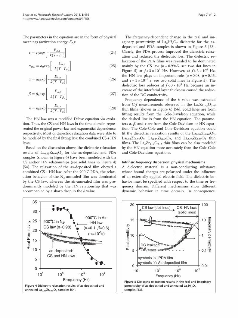
results of La0.35Zr0.65O2 for the as-deposited and PDAsamples (shown in Figure 4) have been modeled with theCS and/or HN relationships (see solid lines in Figure 4)[54]. The relaxation of the as-deposited film obeyed acombined CS + HN law. After the 900°C PDA, the relax-ation behavior of the N2-annealed film was dominatedby the CS law, whereas the air-annealed film was pre-dominantly modeled by the HN relationship that wasaccompanied by a sharp drop in the k value.
0
5
10
15
20
25
30
35
Frequency (Hz)
Re
alP
erm
ittiv
ity
900oC in Air:HN law
( =0.1, =0.6)
( =10-5s)
900oC in N2:CS law (n=0.98)
as-deposited:CS and HN laws
101 103 105 107
βτ
α
Figure 4 Dielectric relaxation results of as-deposited andannealed La0.35Zr0.65O2 samples [54].
The frequency-dependent change in the real and im-aginary permittivity of La2Hf2O7 dielectric for the as-deposited and PDA samples is shown in Figure 5 [53].Clearly, the PDA process improved the dielectric relax-ation and reduced the dielectric loss. The dielectric re-laxation of the PDA films was revealed to be dominatedmainly by the CS law (n = 0.9945, see two dot lines inFigure 5) at f < 3 × 10⁴ Hz. However, at f > 3 × 10⁴ Hz,the HN law plays an important role (α = 0.08, β = 0.45,and τ = 1 × 10⁻⁸ s, see two solid lines in Figure 5). Thedielectric loss reduces at f < 3 × 10⁴ Hz because an in-crease of the interfacial layer thickness caused the reduc-tion of the DC conductivity.Frequency dependence of the k value was extracted
from C-f measurements observed in the LaxZr1−xO2−δ
thin films (shown in Figure 6) [56]. Solid lines are fromfitting results from the Cole-Davidson equation, whilethe dashed line is from the HN equation. The parame-ters α, β, and τ are from the Cole-Davidson or HN equa-tion. The Cole-Cole and Cole-Davidson equation couldfit the dielectric relaxation results of the La0.91Zr0.09O2,La0.22Zr0.78O2, La0.35Zr0.65O2, and La0.63Zr0.37O2 thinfilms. The LaxZr1−xO2−δ thin films can be also modeledby the HN equation more accurately than the Cole-Coleand Cole-Davidson equations.
Intrinsic frequency dispersion: physical mechanismsA dielectric material is a non-conducting substancewhose bound charges are polarized under the influenceof an externally applied electric field. The dielectric be-havior must be specified with respect to the time or fre-quency domain. Different mechanisms show differentdynamic behavior in time domain. In consequence,
0
5
10
15
20
Frequency (Hz)
Rea
lper
mitt
ivity
0.01
0.1
1
10
100
Imaginary
permittivity
symbols 'o': PDA filmsymbols 'x': As-deposited film
DC leakage
CS law (dot lines)
101 103 105 107
CS+HN laws(solid lines)
Figure 5 Dielectric relaxation results in the real and imaginarypermittivity of as-deposited and annealed La2Hf2O7
samples [53].
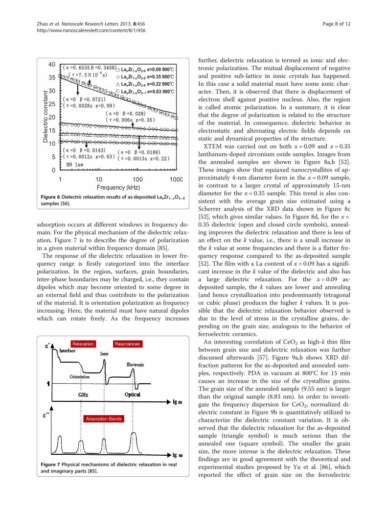
Figure 6 Dielectric relaxation results of as-deposited LaxZr1−xO2−δ
samples [56].
Zhao et al. Nanoscale Research Letters 2013, 8:456 Page 8 of 12http://www.nanoscalereslett.com/content/8/1/456
adsorption occurs at different windows in frequency do-main. For the physical mechanism of the dielectric relax-ation, Figure 7 is to describe the degree of polarizationin a given material within frequency domain [85].The response of the dielectric relaxation in lower fre-
quency range is firstly categorized into the interfacepolarization. In the region, surfaces, grain boundaries,inter-phase boundaries may be charged, i.e., they containdipoles which may become oriented to some degree inan external field and thus contribute to the polarizationof the material. It is orientation polarization as frequencyincreasing. Here, the material must have natural dipoleswhich can rotate freely. As the frequency increases
Figure 7 Physical mechanisms of dielectric relaxation in realand imaginary parts [85].
further, dielectric relaxation is termed as ionic and elec-tronic polarization. The mutual displacement of negativeand positive sub-lattice in ionic crystals has happened.In this case a solid material must have some ionic char-acter. Then, it is observed that there is displacement ofelectron shell against positive nucleus. Also, the regionis called atomic polarization. In a summary, it is clearthat the degree of polarization is related to the structureof the material. In consequence, dielectric behavior inelectrostatic and alternating electric fields depends onstatic and dynamical properties of the structure.XTEM was carried out on both x = 0.09 and x = 0.35
lanthanum-doped zirconium oxide samples. Images fromthe annealed samples are shown in Figure 8a,b [52].These images show that equiaxed nanocrystallites of ap-proximately 4-nm diameter form in the x = 0.09 sample,in contrast to a larger crystal of approximately 15-nmdiameter for the x = 0.35 sample. This trend is also con-sistent with the average grain size estimated using aScherrer analysis of the XRD data shown in Figure 8c[52], which gives similar values. In Figure 8d, for the x =0.35 dielectric (open and closed circle symbols), anneal-ing improves the dielectric relaxation and there is less ofan effect on the k value, i.e., there is a small increase inthe k value at some frequencies and there is a flatter fre-quency response compared to the as-deposited sample[52]. The film with a La content of x = 0.09 has a signifi-cant increase in the k value of the dielectric and also hasa large dielectric relaxation. For the x = 0.09 as-deposited sample, the k values are lower and annealing(and hence crystallization into predominantly tetragonalor cubic phase) produces the higher k values. It is pos-sible that the dielectric relaxation behavior observed isdue to the level of stress in the crystalline grains, de-pending on the grain size, analogous to the behavior offerroelectric ceramics.An interesting correlation of CeO2 as high-k thin film
between grain size and dielectric relaxation was furtherdiscussed afterwards [57]. Figure 9a,b shows XRD dif-fraction patterns for the as-deposited and annealed sam-ples, respectively. PDA in vacuum at 800°C for 15 mincauses an increase in the size of the crystalline grains.The grain size of the annealed sample (9.55 nm) is largerthan the original sample (8.83 nm). In order to investi-gate the frequency dispersion for CeO2, normalized di-electric constant in Figure 9b is quantitatively utilized tocharacterize the dielectric constant variation. It is ob-served that the dielectric relaxation for the as-depositedsample (triangle symbol) is much serious than theannealed one (square symbol). The smaller the grainsize, the more intense is the dielectric relaxation. Thesefindings are in good agreement with the theoretical andexperimental studies proposed by Yu et al. [86], whichreported the effect of grain size on the ferroelectric

Figure 8 XTEM (a,b), XRD (c), and k-f data (d) of annealed andas-deposited samples. (a) XTEM of annealed La0.09Zr0.91O2 sample.(b) XTEM of annealed La0.35Zr0.65O2 sample. (c) XRD of as-depositedLaxZr1−xO2−δ. (d) k-f data of as-deposited and annealedLaxZr1−xO2−δ [52].
Figure 9 XRD of (a) and normalized dielectric constants (b) foras-deposited and annealed CeO2 samples. (b) Under differentfrequencies [57].
Zhao et al. Nanoscale Research Letters 2013, 8:456 Page 9 of 12http://www.nanoscalereslett.com/content/8/1/456
relaxor behavior in CaCu3TiO12 (CCTO) ceramics(shown in inset of Figure 9b). The dielectric relaxationfor the small grain size sample is the worst. The effect ofgrain size mainly originates from higher surface stress insmaller grain due to its higher concentration of grainboundary. Surface stress in grain is high, medium andlow for the small, medium, and large grain size CCTOsamples. As surface stress increases, the glasslike transi-tion temperature decreases considerably. It is attributedto the enhancement of the correlations among polarnanodomains.XRD diffraction patterns for the as-deposited CeO2
thin films at 150, 200, 250, 300, and 350°C, respectively,are shown in the inset of Figure 10a [57]. The grain sizevalue is obtained in Figure 10a using the Scherrer for-mula based on the XRD data. There is a clear trend that
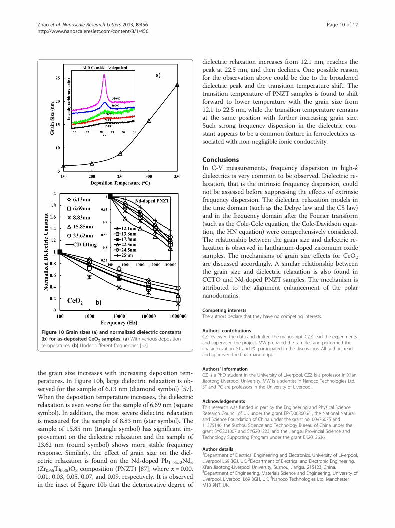
Figure 10 Grain sizes (a) and normalized dielectric constants(b) for as-deposited CeO2 samples. (a) With various depositiontemperatures. (b) Under different frequencies [57].
Zhao et al. Nanoscale Research Letters 2013, 8:456 Page 10 of 12http://www.nanoscalereslett.com/content/8/1/456
the grain size increases with increasing deposition tem-peratures. In Figure 10b, large dielectric relaxation is ob-served for the sample of 6.13 nm (diamond symbol) [57].When the deposition temperature increases, the dielectricrelaxation is even worse for the sample of 6.69 nm (squaresymbol). In addition, the most severe dielectric relaxationis measured for the sample of 8.83 nm (star symbol). Thesample of 15.85 nm (triangle symbol) has significant im-provement on the dielectric relaxation and the sample of23.62 nm (round symbol) shows more stable frequencyresponse. Similarly, the effect of grain size on the diel-ectric relaxation is found on the Nd-doped Pb1−3x/2Ndx(Zr0.65Ti0.35)O3 composition (PNZT) [87], where x = 0.00,0.01, 0.03, 0.05, 0.07, and 0.09, respectively. It is observedin the inset of Figure 10b that the deteriorative degree of
dielectric relaxation increases from 12.1 nm, reaches thepeak at 22.5 nm, and then declines. One possible reasonfor the observation above could be due to the broadeneddielectric peak and the transition temperature shift. Thetransition temperature of PNZT samples is found to shiftforward to lower temperature with the grain size from12.1 to 22.5 nm, while the transition temperature remainsat the same position with further increasing grain size.Such strong frequency dispersion in the dielectric con-stant appears to be a common feature in ferroelectrics as-sociated with non-negligible ionic conductivity.
ConclusionsIn C-V measurements, frequency dispersion in high-kdielectrics is very common to be observed. Dielectric re-laxation, that is the intrinsic frequency dispersion, couldnot be assessed before suppressing the effects of extrinsicfrequency dispersion. The dielectric relaxation models inthe time domain (such as the Debye law and the CS law)and in the frequency domain after the Fourier transform(such as the Cole-Cole equation, the Cole-Davidson equa-tion, the HN equation) were comprehensively considered.The relationship between the grain size and dielectric re-laxation is observed in lanthanum-doped zirconium oxidesamples. The mechanisms of grain size effects for CeO2
are discussed accordingly. A similar relationship betweenthe grain size and dielectric relaxation is also found inCCTO and Nd-doped PNZT samples. The mechanism isattributed to the alignment enhancement of the polarnanodomains.
Competing interestsThe authors declare that they have no competing interests.
Authors' contributionsCZ reviewed the data and drafted the manuscript. CZZ lead the experimentsand supervised the project. MW prepared the samples and performed thecharacterization. ST and PC participated in the discussions. All authors readand approved the final manuscript.
Authors’ informationCZ is a PhD student in the University of Liverpool. CZZ is a professor in Xi'anJiaotong-Liverpool University. MW is a scientist in Nanoco Technologies Ltd.ST and PC are professors in the University of Liverpool.
AcknowledgementsThis research was funded in part by the Engineering and Physical ScienceResearch Council of UK under the grant EP/D068606/1, the National Naturaland Science Foundation of China under the grant no. 60976075 and11375146, the Suzhou Science and Technology Bureau of China under thegrant SYG201007 and SYG201223, and the Jiangsu Provincial Science andTechnology Supporting Program under the grant BK2012636.
Author details1Department of Electrical Engineering and Electronics, University of Liverpool,Liverpool L69 3GJ, UK. 2Department of Electrical and Electronic Engineering,Xi’an Jiaotong-Liverpool University, Suzhou, Jiangsu 215123, China.3Department of Engineering, Materials Science and Engineering, University ofLiverpool, Liverpool L69 3GH, UK. 4Nanoco Technologies Ltd, ManchesterM13 9NT, UK.

Zhao et al. Nanoscale Research Letters 2013, 8:456 Page 11 of 12http://www.nanoscalereslett.com/content/8/1/456
Received: 3 October 2013 Accepted: 18 October 2013Published: 1 November 2013
References1. Juan PC, Liu CH, Lin CL, Ju SC, Chen MG, Chang IYK, Lu JH: Electrical
characterization and dielectric property of MIS capacitors using a high-kCeZrO4 ternary oxide as the gate dielectric. Jpn J Appl Phys 2009, 48(05DA02):1–5.
2. Dong GF, Qiu Y: Pentacene thin-film transistors with Ta2O5 as the gatedielectric. J Kor Phys Soc 2009, 54(1):493–497.
3. Zhu XH, Zhu JM, Li AD, Liu ZG, Ming NB: Challenges in atomic-scalecharacterization of high-k dielectrics and metal gate electrodes foradvanced CMOS gate stacks. J Mater Sci Technol 2009, 25(3):289–313.
4. International Technology Roadmap for Semiconductors.[http://public.itrs.net/]
5. Rahmani M, Ahmadi MT, Abadi HKF, Saeidmanesh M, Akbari E, Ismail R:Analytical modeling of trilayer graphene nanoribbon Schottky-barrierFET for high-speed switching applications. Nanoscale Res Lett 2013, 8:55.
6. Ding SJ, Chen HB, Cui XM, Chen S, Sun QQ, Zhou P, Lu HL, Zhang DW,Shen C: Atomic layer deposition of high-density Pt nanodots on Al2O3
film using (MeCp)Pt(Me)3 and O2 precursors for nonvolatile memoryapplications. Nanoscale Res Lett 2013, 8:80.
7. Chalker PR, Werner M, Romani S, Potter RJ, Black K, Aspinall HC, Jones AC,Zhao CZ, Taylor S, Heys PN: Permittivity enhancement of hafnium dioxidehigh-k films by cerium doping. Appl Phys Lett 2008, 93:182911.
8. Chen SH, Liao WS, Yang HC, Wang SJ, Liaw YG, Wang H, Gu HS, Wang MC:High-performance III-V MOSFET with nano-stacked high-k gate dielectricand 3D fin-shaped structure. Nanoscale Res Lett 2012, 7:431.
9. Wang JC, Lin CT, Chen CH: Gadolinium oxide nanocrystal nonvolatilememory with HfO2/Al2O3 nanostructure tunneling layers. Nanoscale ResLett 2012, 7:177.
10. Shi L, Liu ZG: Characterization upon electrical hysteresis and thermaldiffusion of TiAl3Ox dielectric film. Nanoscale Res Lett 2011, 6:557.
11. Khomenkova L, Sahu BS, Slaoui A, Gourbilleau F: Hf-based high-k materialsfor Si nanocrystal floating gate memories. Nanoscale Res Lett 2011, 6:172.
12. Chen FH, Her JL, Shao YH, Matsuda YH, Pan TM: Structural and electricalcharacteristics of high-k Er2O3 and Er2TiO5 gate dielectrics for a-IGZOthin-film transistors. Nanoscale Res Lett 2013, 8:18.
13. Dalapati G, Wong TS, Li Y, Chia C, Das A, Mahata C, Gao H, ChattopadhyayS, Kumar M, Seng H, Maiti C, Chi D: Characterization of epitaxial GaAsMOS capacitors using atomic layer-deposited TiO2/Al2O3 gate stack:study of Ge auto-doping and p-type Zn doping. Nanoscale Res Lett 2012,7:99.
14. An YT, Labbé C, Khomenkova L, Morales M, Portier X, Gourbilleau F:Microstructure and optical properties of Pr3+-doped hafnium silicatefilms. Nanoscale Res Lett 2013, 8:43.
15. Zhou P, Ye L, Sun QQ, Wang PF, Jiang AQ, Ding SJ, Zhang DW: Effect ofconcurrent joule heat and charge trapping on RESET for NbAlOfabricated by atomic layer deposition. Nanoscale Res Lett 2013, 8:91.
16. King PJ, Werner M, Chalker PR, Jones AC, Aspinall HC, Basca J, Wrench JS,Black K, Davies HO, Heys PN: Effect of deposition temperature on theproperties of CeO2 films grown by atomic layer deposition. Thin SolidFilms 2011, 519:4192–4195.
17. Aspinall HC, Bacsa J, Jones AC, Wrench JS, Black K, Chalker PR, King PJ,Marshall P, Werner M, Davies HO, Odedra R: Ce(IV) complexes withdonor-functionalized alkoxide ligands: improved precursors for chemicalvapor deposition of CeO2. Inorg Chem 2011, 50:11644–11652.
18. Phokha S, Pinitsoontorn S, Chirawatkul P, Poo-arporn Y, Maensiri S: Synthesis,characterization, and magnetic properties of monodisperse CeO2
nanospheres prepared by PVP-assisted hydrothermal method. NanoscaleRes Lett 2012, 7:425.
19. Fukuda H, Miura M, Sakuma S, Nomura S: Structural and electricalproperties of crystalline CeO2 films formed by metaorganicdecomposition. Jpn J Appl Phys 1998, 37:4158–4159.
20. Santha NI, Sebastian MT, Mohanan P, Alford NM, Sarma K, Pullar RC, KambaS, Pashkin A, Samukhina P, Petzelt J: Effect of doping on the dielectricproperties of cerium oxide in the microwave and far-infrared frequencyrange. J Am Ceram Soc 2004, 87:1233–1237.
21. Nishikawa Y, Fukushima N, Yasuda N, Nakayama K, Ikegawa S: Electricalproperties of single crystalline CeO2 high-k gate dielectrics directlygrown on Si (111). Jpn J Appl Phys 2002, 41:2480–2483.
22. Jacqueline S, Black WK, Aspinall HC, Jones AC, Bacsa J, Chalker PR, King PJ,Werner M, Davies HO, Heys PN: MOCVD and ALD of CeO2 thin films usinga novel monomeric CeIV alkoxide precursor. Chem Vap Deposition 2009,15:259–261.
23. Tye L, ElMasry NA, Chikyow T, McLarty P, Bedair SM: Electricalcharacteristics of epitaxial CeO2 on Si(111). Appl Phys Lett 1994, 65:3081.
24. Gross MS, Ulla MA, Querini CA: Catalytic oxidation of diesel soot: newcharacterization and kinetic evidence related to the reaction mechanismon K/CeO2 catalyst. Appl Catal Gen 2009, 1(360):81–88.
25. Pan TM, Liao CS, Hsu HH, Chen CL, Lee JD, Wang KT, Wang JC: Excellentfrequency dispersion of thin gadolinium oxide high-k gate dielectrics.Appl Phys Lett 2005, 26(87):262908–262908.
26. Koveshnikov S, Tsai WOI, Lee JC, Torkanov V, Yakimov M, Oktyabrsky S:Metal-oxide-semiconductor capacitors on GaAs with high-k gate oxideand amorphous silicon interface passivation layer. Appl Phys Lett 2006,2(88):022106–022106.
27. Robertson J, Falabretti B: Band offsets of high-k gate oxides on III-V semi-conductors. J Appl Phys 2006, 1(100):014111–014111.
28. Pan TM, Chen CL, Yeh WW, Hou SJ: Structural and electrical characteristicsof thin erbium oxide gate dielectrics. Appl Phys Lett 2006,22(89):22912–222912.
29. Liu CH, Pan TM, Shu WH, Huang KC: Electrochem Solid-State Lett 2007,8(10):G54–G57.
30. Anthony J, Aspinall HC, Chalker PR, Potter RJ, Manning TD, Loo YF, O’KaneR, Gaskell JM, Smith LM: MOCVD and ALD of high-k dielectric oxidesusing alkoxide precursors. Chem Vap Depos 2006, 12:83–98.
31. Laha A, Bugiel E, Osten HJ, Fissel A: Crystalline ternary rare earth oxidewith capacitance equivalent thickness below 1 nm for high-kapplication. Appl Phys Lett 2006, 17(88):172107–172107.
32. Souza D, Kiewra JPE, Sun Y, Callegari A, Sadana DK, Shahidi G, Webb DJ:Inversion mode n-channel GaAs field effect transistor with high-k/metalgate. Appl Phys Lett 2008, 15(92):153508–153508.
33. Adamopoulos G, Thomas S, Bradley DD, McLachlan MA, Anthopoulos TD:Low-voltage ZnO thin-film transistors based on Y2O3 and Al2O3 high-kdielectrics deposited by spray pyrolysis in air. Appl Phys Lett 2011,98:123503.
34. Yan L, Lu HB, Tan GT, Chen F, Zhou YL, Yang GZ, Liu W, Chen ZH: Highquality, high-k gate dielectric: amorphous LaAlO3 thin films grown on Si(100) without Si interfacial layer. Applied Physics A 2003, 5(77):721–724.
35. Lu XB, Liu ZG, Zhang X, Huang R, Zhou HW, Wang XP, Nguyen BY:Investigation of high-quality ultra-thin LaAlO3 films as high-k gatedielectrics. J Phys D Appl Phys 2003, 36(23):3047.
36. Gougousi T, Kelly MJ, Terry DB, Parsons GN: Properties of La-silicate high-kdielectric films formed by oxidation of La on silicon. J Appl Phys 2003,3(93):1691–1696.
37. Mahata CM, Bera K, Das T, Mallik S, Hota MK, Majhi B, Verma S, Bose PK,Maiti CK: Charge trapping and reliability characteristics of sputtered Y2O3
high-k dielectrics on N- and S-passivated germanium. Semicond SciTechnol 2009, 8(24):085006.
38. Pan TM, Lei TF, Chao TS, Chang KL, Hsieh KC: High quality ultrathin CoTiO3
high-k gate dielectrics. Electrochem Solid-State Lett 2000, 9(3):433–434.39. Kim SK, Kim KM, Kwon OS, Lee SW, Jeon CB, Park WY, Hwang CS, Jeong J:
Structurally and electrically uniform deposition of high-k TiO2 thin filmson a Ru electrode in three-dimensional contact holes using atomic layerdeposition. Electrochem Solid-State Lett 2005, 12(8):F59–F62.
40. Abermann S, Pozzovivo G, Kuzmik J, Strasser G, Pogany D, Carlin JF,Grandjean N, Bertagnolli E: MOCVD of HfO2 and ZrO2 high-k gatedielectrics for InAlN/AlN/GaN MOS-HEMTs. Semicond Sci Technol 2007,12(22):1272.
41. Adamopoulos G, Thomas S, Wöbkenberg PH, Bradley DD, McLachlan MA,Anthopoulos TD: High-mobility low-voltage ZnO and Li-doped ZnOtransistors based on ZrO2 high-k dielectric grown by spray pyrolysis inambient air. Adv Mater 2011, 16(23):1894–1898.
42. Gaskell JM, Jones AC, Aspinall HC, Taylor S, Taechakumput P, Chalker PR,Heys PN, Odedra R: Deposition of lanthanum zirconium oxide high-kfilms by liquid injection atomic layer deposition. Appl Phys Lett 2007,11(91):112912–112912.
43. Gaskell JM, Jones AC, Chalker PR, Werner M, Aspinall HC, Taylor S,Taechakumput P, Heys PN: Deposition of lanthanum zirconium oxidehigh-k films by liquid injection ALD and MOCVD. Chem Vap Depos 2007,12(13):684–690.

Zhao et al. Nanoscale Research Letters 2013, 8:456 Page 12 of 12http://www.nanoscalereslett.com/content/8/1/456
44. Gutowski M, Jaffe JE, Liu CL, Stoker M, Hegde RI, Rai RS, Tobin PJ:Thermodynamic stability of high-k dielectric metal oxides ZrO2 and HfO2
in contact with Si and SiO2. MRS Proceedings 2002, 716(1). doi: http://dx.doi.org/10.1557/PROC-716-B3.2.
45. Dimoulas A, Vellianitis G, Mavrou G, Apostolopoulos G, Travlos A, Wiemer C,Fanciulli M, Rittersma ZM: La2Hf2O7 high-k gate dielectric grown directlyon Si (001) by molecular-beam epitaxy. Appl Phys Lett 2004,15(85):3205–3207.
46. Gang H, Deng B, Sun ZQ, Chen XS, Liu YM, Zhang LD: CVD-derivedHf-based high-k gate dielectrics. Crit Rev Solid State Mater Sci 2013,4(38):235–261.
47. Watanabe H, Saitoh M, Ikarashi N, Tatsumi T: High-quality HfSixOy gatedielectrics fabricated by solid phase interface reaction between physical–vapor -deposited metal-Hf and SiO2 underlayer. Appl Phys Lett 2004,3(85):449–451.
48. Darbandy G, Ritzenthaler R, Lime F, Garduño I, Estrada M, Cerdeira A,Iñiguez B: Analytical modeling of direct tunneling current through gatestacks for the determination of suitable high-k dielectrics for nanoscaledouble-gate MOSFETs. Semicond Sci Technol 2011, 4(26):045002.
49. Myllymäki P, Roeckerath M, Putkonen M, Lenk S, Schubert J, Niinistö L,Mantl S: Characterization and electrical properties of high-k GdScO3 thinfilms grown by atomic layer deposition. Applied Physics A 2007,4(88):633–637.
50. Chan KC, Lee PF, Li DF, Dai JY: Memory characteristics and the tunnelingmechanism of Au nanocrystals embedded in a DyScO3 high-k gatedielectric layer. Semicond Sci Technol 2011, 2(26):025015.
51. Milanov AP, Xu K, Cwik S, Parala H, de los Arcos T, Becker HW, Devi A:Sc2O3, Er2O3, and Y2O3 thin films by MOCVD from volatile guanidinateclass of rare-earth precursors. Dalton Trans 2012, 45(41):13936–13947.
52. Zhao CZ, Taylor S, Werner M, Chalker PR, Murray RT, Gaskell JM, Jones AC:Dielectric relaxation of lanthanum doped zirconium oxide. J Appl Phys2009, 105:044102.
53. Zhao CZ, Taylor S, Werner M, Chalker PR, Gaskell JM, Jones AC: Frequencydispersion and dielectric relaxation of La2Hf2O7. J Vac Sci Technol B 2009,1(27):333.
54. Zhao CZ, Werner M, Taylor S, Chalker PR, Jones AC, Zhao C: Dielectricrelaxation of La-doped Zirconia caused by annealing ambient. NanoscaleRes Lett 2011, 6:48.
55. Zhao C, Zhao CZ, Tao J, Werner M, Taylor S, Chalker PR: Dielectricrelaxation of lanthanide-based ternary oxides: physical and mathemat-ical models. J Nanomater 2012:241470.
56. Tao J, Zhao CZ, Zhao C, Taechakumput P, Werner M, Taylor S, Chalker PR:Extrinsic and intrinsic frequency dispersion of high-k materials incapacitance-voltage measurements. Materials 2012, 5:1005–1032.
57. Zhao C, Zhao CZ, Werner M, Taylor S, Chalker PR, King P: Grain sizedependence of dielectric relaxation in cerium oxide as high-k layer.Nanoscale Res Lett 2013, 8:172.
58. Schuegraf KF, King CC, Hu C: Impact of polysilicon depeletion in thinoxide MOS device. In VLSI Technology, Seattle, WA; 2–4 June 1992.Piscataway: IEEE; 1996:86–90.
59. Lee SW, Liang C, Pan CS, Lin W, Mark JB: A study on the physicalmechanism in the recovery of gate capacitance to COX in implantpolysilicon MOS structure. IEEE Electron Device Lett 1992, 1(13):2–4.
60. Spinelli AS, Pacelli A, Lacaita AL: An improved formula for thedetermination of the polysilicon doping. IEEE Electron Device Lett 2001,6(22):281–283.
61. Pregaldiny F, Lallement C, Mathiot D: Accounting for quantum mechanicaleffects from accumulation to inversion, in a fully analytical surfacepotential-based MOSFET model. Solid State Electron 2004, 5(48):781–787.
62. Sune J, Olivo P, Ricco B: Quantum-mechanical modeling of accumulationlayers in MOS structure. IEEE Trans. Electron Devices 1992, 7(39):1732–1739.
63. Pregaldiny F, Lallement C, van Langevelde R, Mathiot D: An advancedexplicit surface potential model physically accounting for thequantization effects in deep-submicron. Solid State Electron 2004,3(48):427–435.
64. Wu WH, Tsui BY, Huang YP, Hsieh FC, Chen MC, Hou YT, Jin Y, Tao HJ, ChenSC, Liang MS: Two-frequency C-V correction using five-element circuitmodel for high-k gate dielectric and ultrathin oxide. IEEE Electron DeviceLett 2006, 5(27):399–401.
65. Lerner EJ: The end of the road for Moore's law. IBM J. Res. Develop 1999,4:6–11.
66. Ahmed K, Ibok E, Yeap GCF, Qi X, Ogle B, Wortman JJ, Hauser JR: Impact oftunnel currents and channel resistance on the characterization of channelinversion layer charge and polysilicon-gate depletion of sub-20-A gateoxide MOSFET’s. IEEE Trans. Electron Devices 1999, 8(46):1650–1655.
67. Choi CH, Goo JS, Oh TY, Yu ZP, Dutton RW, Bayoumi A, Cao M, Voorde PV,Vook D, Diaz CH: MOS C-V characterization of ultrathin gate oxidethickness (1.3-1.8 nm). IEEE Electron Device Lett 1999, 6(20):292–294.
68. Taechakumput P, Zhao CZ, Taylor S, Werner M, Pham N, Chalker PR, MurrayRT, Gaskell JM, Aspinall HC, Jones AC: Origin of frequency of dispersion inhigh-k dielectrics. In Proceedings of 7th International SemiconductorTechnology Conference ISTC2008. Pudong. Shanghai; 2008.
69. Yang KJ, Hu CM: MOS capacitance measurements for high-leakage thindielectrics. IEEE Trans. Electron Devices 1999, 7(46):1500–1501.
70. Hirose M, Hiroshima M, Yasaka T, Miyazaki S: Characterization of siliconsurface microroughness and tunneling transport through ultrathin gateoxide. J Vac Sci Technol A 1994, 4(12):1864–1868.
71. Curie JR: sur le pouvoir inducteur specifique et sur la conductibilite descorps cristallises. Ann Chim Phys 1889, 18:203.
72. Von Schweidler E: Studien uber die anomalien im verhalten derdielektrika. Ann Phys 1907, 24:711–770.
73. Debye P: Polar Molecules. New York, NY, USA: Chemical CatalogueCompany; 1929.
74. Williams G, Watts DC: Non-symmetrical dielectric relaxation behaviourarising from a simple empirical decay function. Trans Faraday Soc 1969,66:80–85.
75. Bokov AA, Ye ZG: Double freezing of dielectric response in relaxor Pb(Mg1/3Nb2/3)O3 crystals. Phys Rev B 2006, 13(74):132102.
76. Ngai KL, Plazek DJ: A quantitative explanation of the difference in thetemperature dependences of the viscoelastic softening and terminaldispersions of linear amorphous polymers. J Polym Sci Polym Phys 1986,3(24):619–632.
77. Cole KS, Cole RH: Dispersion and absorption in dielectrics. J Chem Phys1941, 9:341–351.
78. Davidson DW, Cole RH: Dielectric relaxation in glycerine. J Chem Phys1950, 18:1417.
79. Davidson DW, Cole RH: Dielectric relaxation in glycerol, propylene glycoland n-propanol. J Chem Phys 1951, 19:1484–1490.
80. Dotson TC, Budzien J, McCoy JD, Adolf DB: Cole-Davidson dynamics ofsimple chain models. J Chem Phys 2009, 130:024903.
81. Ngai KL, McKenna GB, McMillan PF, Martin S: Relaxation in glassformingliquids and amorphous solids. J Appl Phys 2000, 88:3113–3157.
82. Havriliak S, Negami S: A complex plane analysis of α-dispersions in somepolymer systems. J Polym Sci Pt C 1966, 1(14):99–117.
83. Havriliak S, Negami S: A complex plane representation of dielectricmechanical relaxation processes in some polymers. Polymer 1967,8:161–210.
84. Hartmann B, Lee GF, Lee JD: Loss factor height and width limits forpolymer relaxations. J Acoust Soc Am 1994, 1(95):226–233.
85. Schroeder T: Physics of dielectric and DRAM. Frankfurt, Germany: IHP ImTechnologiepark; 2010.
86. Yu HT, Liu HX, Hao H, Guo LL, Jin CJ: Grain size dependence of relaxorbehavior in CaCu3Ti4O12 ceramics. Appl Phys Lett 2007, 91:222911.
87. Mohiddon MA, Kumar A, Yadav KL: Effect of Nd doping on structural,dielectric and thermodynamic properties of PZT (65/35) ceramic. PhysicaB 2007, 395:1–9.
doi:10.1186/1556-276X-8-456Cite this article as: Zhao et al.: Dielectric relaxation of high-k oxides.Nanoscale Research Letters 2013 8:456.