
Diamond Field-Effect Transistors With V 2 O 5 -Induced ...
6
2270 IEEE TRANSACTIONS ON ELECTRON DEVICES, VOL. 67, NO. 6, JUNE 2020 Diamond Field-Effect Transistors With V 2 O 5 -Induced Transfer Doping: Scaling to 50-nm Gate Length Kevin G. Crawford , James D. Weil, Pankaj B. Shah, Dmitry A. Ruzmetov, Mahesh R. Neupane, Khamsouk Kingkeo, A. Glen Birdwell, and Tony G. Ivanov Abstract — We report on the fabrication and measurement of hydrogen-terminated diamond field-effect transistors (FETs) incorporating V 2 O 5 as a surface acceptor material to induce transfer doping. Comparing a range of gate lengths down to 50 nm, we observe inversely scaling peak output current and transconductance. Devices exhibited a peak drain current of ∼700 mA/mm and a peak transconductance of ∼150 mS/mm, some of the highest reported thus far for a diamond metal semiconductor FET (MESFET). Reduced sheet resistance of the diamond surface after V 2 O 5 deposition was verified by four probe measurement. These results show great potential for improvement of diamond FET devices through scaling of critical dimensions and adoption of robust transition metal oxides such as V 2 O 5 . Index Terms— 2-D hole gas (2DHG), diamond metal semi- conductor field-effect transistor (MESFET), drain-induced barrier lowering (DIBL), electronic devices, gate length, power, radio frequency (RF), surface transfer doping, V 2 O 5 . I. I NTRODUCTION I NTEREST in the diamond material system for elec- tronic applications has rapidly increased in recent years, becoming a global scale area of interest. With its ultrawide band-gap of 5.47 eV, extremely high thermal conductivity of >20 W cm −1 K −1 and intrinsically high breakdown field of 10 MV/cm, diamond is a promising candidate in achiev- ing next-generation high-power electronic devices [1]–[4]. Progress in this area has been typically hindered by the lack of mature doping techniques and on-going development of novel fabrication strategies to overcome the challenges in working with diamond [5]. The U.S. Army Research Laboratory is investing in the development of surface transfer-doped dia- mond field-effect transistors (FETs) for radio frequency (RF) and power applications [6]–[8]. Surface transfer doping offers an alternative to substitutional doping that alleviates the chal- lenges of introducing impurity dopants into diamond’s tightly packed carbon lattice. Historically, spontaneous accumulation Manuscript received March 3, 2020; revised April 13, 2020; accepted April 19, 2020. Date of publication May 6, 2020; date of current ver- sion May 21, 2020. The review of this article was arranged by Editor G. Ghione. (Kevin G. Crawford and James D. Weil contributed equally to this work.) (Corresponding author: Kevin G. Crawford.) The authors are with the CCDC U.S. Army Research Laboratory, Adelphi, MD 20783 USA (e-mail: [email protected]). Color versions of one or more of the figures in this article are available online at http://ieeexplore.ieee.org. Digital Object Identifier 10.1109/TED.2020.2989736 of volatile atmospheric adsorbents on the hydrogen-terminated diamond surface when exposed to air has provided the nec- essary surface acceptor states for transfer doping [1], [9]. However, this method of transfer doping is highly sensitive to environmental conditions such as temperature, humidity, and molecular composition of the adsorbents [8], [9]. More recent results demonstrate enhanced surface transfer doping utilizing high electron affinity transition metal oxides, such as V 2 O 5 . When in intimate contact with the hydrogen-terminated diamond surface, these high electron affinity materials will prompt the transfer of electrons from the diamond, acting as an electron accepter. This process leaves behind corre- sponding holes within the diamond, forming a 2-D hole gas (2DHG) beneath the surface [8], [10], [11]. This approach of encapsulation with a transition metal oxide has been incorpo- rated into our diamond metal semiconductor FET (MESFET) designs, improving output current density and stability of devices. By reducing gate length ( L g ), peak output current and transconductance are improved significantly. II. EXPERIMENTAL A single crystal diamond sample with (100) surface ori- entation and 4 mm × 4 mm dimensions was obtained from Element Six. The substrate was first cleaned in H 2 SO 4 :NHO 3 , to remove any metallic and organic contaminants, and then hydrogen terminated in a CVD diamond growth reactor. The substrate was then coated with 100 nm thermally evaporated Au as a sacrificial layer both to form ohmic contacts and to protect the hydrogen-terminated surface. Electrical isolation of devices was performed by patterning and etching the Au sacrificial layer between regions using a KI 2 solution. At this point, the exposed diamond surface is treated in O 2 plasma to remove hydrogen termination in these areas. Probe pads consisting of Ti/Au were written and deposited to overlap the Au ohmic metal and provide a more robust contact. The source–drain region of each device was then patterned and etched using a KI 2 solution with carefully controlled dilution and temperature. Gate dimensions of 50, 100, 200, 400, and 800 nm were defined by e-beam lithography and a metal gate-stack of Al/Pt/Au 50/25/45 nm was deposited. A similar process flow can be found in [6]. Each device had two gates with a combined width of 50 μm and a This work is licensed under a Creative Commons Attribution 4.0 License. For more information, see https://creativecommons.org/licenses/by/4.0/
Transcript of Diamond Field-Effect Transistors With V 2 O 5 -Induced ...

2270 IEEE TRANSACTIONS ON ELECTRON DEVICES, VOL. 67, NO. 6, JUNE 2020
Diamond Field-Effect Transistors WithV2O5-Induced Transfer Doping:Scaling to 50-nm Gate Length
Kevin G. Crawford , James D. Weil, Pankaj B. Shah, Dmitry A. Ruzmetov, Mahesh R. Neupane,Khamsouk Kingkeo, A. Glen Birdwell, and Tony G. Ivanov
Abstract— We report on the fabricationand measurementof hydrogen-terminated diamond field-effect transistors(FETs) incorporating V2O5 as a surface acceptor material toinduce transfer doping. Comparing a range of gate lengthsdown to 50 nm, we observe inversely scaling peak outputcurrent and transconductance. Devices exhibited a peakdrain current of ∼700 mA/mm and a peak transconductanceof ∼150 mS/mm, some of the highest reported thus far fora diamond metal semiconductor FET (MESFET). Reducedsheet resistance of the diamond surface after V2O5deposition was verified by four probe measurement. Theseresults show great potential for improvement of diamondFET devices through scaling of critical dimensions andadoption of robust transition metal oxides such as V2O5.
Index Terms— 2-D hole gas (2DHG), diamond metal semi-conductor field-effect transistor (MESFET), drain-inducedbarrier lowering (DIBL), electronic devices, gate length,power, radio frequency (RF), surface transfer doping, V2O5.
I. INTRODUCTION
INTEREST in the diamond material system for elec-tronic applications has rapidly increased in recent years,
becoming a global scale area of interest. With its ultrawideband-gap of 5.47 eV, extremely high thermal conductivityof >20 W cm−1 K−1 and intrinsically high breakdown fieldof 10 MV/cm, diamond is a promising candidate in achiev-ing next-generation high-power electronic devices [1]–[4].Progress in this area has been typically hindered by the lack ofmature doping techniques and on-going development of novelfabrication strategies to overcome the challenges in workingwith diamond [5]. The U.S. Army Research Laboratory isinvesting in the development of surface transfer-doped dia-mond field-effect transistors (FETs) for radio frequency (RF)and power applications [6]–[8]. Surface transfer doping offersan alternative to substitutional doping that alleviates the chal-lenges of introducing impurity dopants into diamond’s tightlypacked carbon lattice. Historically, spontaneous accumulation
Manuscript received March 3, 2020; revised April 13, 2020; acceptedApril 19, 2020. Date of publication May 6, 2020; date of current ver-sion May 21, 2020. The review of this article was arranged by EditorG. Ghione. (Kevin G. Crawford and James D. Weil contributed equally tothis work.) (Corresponding author: Kevin G. Crawford.)
The authors are with the CCDC U.S. Army Research Laboratory,Adelphi, MD 20783 USA (e-mail: [email protected]).
Color versions of one or more of the figures in this article are availableonline at http://ieeexplore.ieee.org.
Digital Object Identifier 10.1109/TED.2020.2989736
of volatile atmospheric adsorbents on the hydrogen-terminateddiamond surface when exposed to air has provided the nec-essary surface acceptor states for transfer doping [1], [9].However, this method of transfer doping is highly sensitiveto environmental conditions such as temperature, humidity,and molecular composition of the adsorbents [8], [9]. Morerecent results demonstrate enhanced surface transfer dopingutilizing high electron affinity transition metal oxides, such asV2O5. When in intimate contact with the hydrogen-terminateddiamond surface, these high electron affinity materials willprompt the transfer of electrons from the diamond, actingas an electron accepter. This process leaves behind corre-sponding holes within the diamond, forming a 2-D hole gas(2DHG) beneath the surface [8], [10], [11]. This approach ofencapsulation with a transition metal oxide has been incorpo-rated into our diamond metal semiconductor FET (MESFET)designs, improving output current density and stability ofdevices. By reducing gate length (Lg), peak output currentand transconductance are improved significantly.
II. EXPERIMENTAL
A single crystal diamond sample with (100) surface ori-entation and 4 mm × 4 mm dimensions was obtained fromElement Six. The substrate was first cleaned in H2SO4:NHO3,to remove any metallic and organic contaminants, and thenhydrogen terminated in a CVD diamond growth reactor. Thesubstrate was then coated with 100 nm thermally evaporatedAu as a sacrificial layer both to form ohmic contacts and toprotect the hydrogen-terminated surface. Electrical isolationof devices was performed by patterning and etching the Ausacrificial layer between regions using a KI2 solution. At thispoint, the exposed diamond surface is treated in O2 plasmato remove hydrogen termination in these areas. Probe padsconsisting of Ti/Au were written and deposited to overlapthe Au ohmic metal and provide a more robust contact.The source–drain region of each device was then patternedand etched using a KI2 solution with carefully controlleddilution and temperature. Gate dimensions of 50, 100, 200,400, and 800 nm were defined by e-beam lithography anda metal gate-stack of Al/Pt/Au 50/25/45 nm was deposited.A similar process flow can be found in [6]. Each devicehad two gates with a combined width of 50 μm and a
This work is licensed under a Creative Commons Attribution 4.0 License. For more information, see https://creativecommons.org/licenses/by/4.0/
CRAWFORD et al.: DIAMOND FETs WITH V2O5-INDUCED TRANSFER DOPING 2271
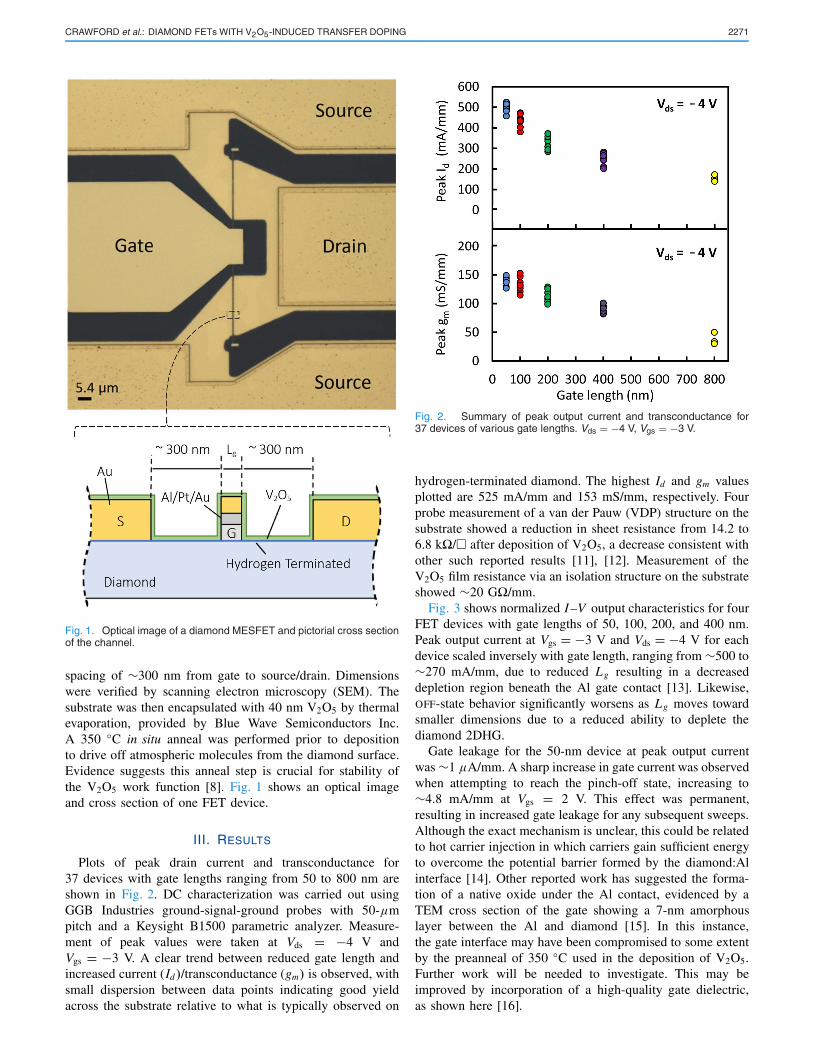
Fig. 1. Optical image of a diamond MESFET and pictorial cross sectionof the channel.
spacing of ∼300 nm from gate to source/drain. Dimensionswere verified by scanning electron microscopy (SEM). Thesubstrate was then encapsulated with 40 nm V2O5 by thermalevaporation, provided by Blue Wave Semiconductors Inc.A 350 ◦C in situ anneal was performed prior to depositionto drive off atmospheric molecules from the diamond surface.Evidence suggests this anneal step is crucial for stability ofthe V2O5 work function [8]. Fig. 1 shows an optical imageand cross section of one FET device.
III. RESULTS
Plots of peak drain current and transconductance for37 devices with gate lengths ranging from 50 to 800 nm areshown in Fig. 2. DC characterization was carried out usingGGB Industries ground-signal-ground probes with 50-μmpitch and a Keysight B1500 parametric analyzer. Measure-ment of peak values were taken at Vds = −4 V andVgs = −3 V. A clear trend between reduced gate length andincreased current (Id)/transconductance (gm) is observed, withsmall dispersion between data points indicating good yieldacross the substrate relative to what is typically observed on
Fig. 2. Summary of peak output current and transconductance for37 devices of various gate lengths. Vds = −4 V, Vgs = −3 V.
hydrogen-terminated diamond. The highest Id and gm valuesplotted are 525 mA/mm and 153 mS/mm, respectively. Fourprobe measurement of a van der Pauw (VDP) structure on thesubstrate showed a reduction in sheet resistance from 14.2 to6.8 k�/� after deposition of V2O5, a decrease consistent withother such reported results [11], [12]. Measurement of theV2O5 film resistance via an isolation structure on the substrateshowed ∼20 G�/mm.
Fig. 3 shows normalized I–V output characteristics for fourFET devices with gate lengths of 50, 100, 200, and 400 nm.Peak output current at Vgs = −3 V and Vds = −4 V for eachdevice scaled inversely with gate length, ranging from ∼500 to∼270 mA/mm, due to reduced Lg resulting in a decreaseddepletion region beneath the Al gate contact [13]. Likewise,OFF-state behavior significantly worsens as Lg moves towardsmaller dimensions due to a reduced ability to deplete thediamond 2DHG.
Gate leakage for the 50-nm device at peak output currentwas ∼1 μA/mm. A sharp increase in gate current was observedwhen attempting to reach the pinch-off state, increasing to∼4.8 mA/mm at Vgs = 2 V. This effect was permanent,resulting in increased gate leakage for any subsequent sweeps.Although the exact mechanism is unclear, this could be relatedto hot carrier injection in which carriers gain sufficient energyto overcome the potential barrier formed by the diamond:Alinterface [14]. Other reported work has suggested the forma-tion of a native oxide under the Al contact, evidenced by aTEM cross section of the gate showing a 7-nm amorphouslayer between the Al and diamond [15]. In this instance,the gate interface may have been compromised to some extentby the preanneal of 350 ◦C used in the deposition of V2O5.Further work will be needed to investigate. This may beimproved by incorporation of a high-quality gate dielectric,as shown here [16].

2272 IEEE TRANSACTIONS ON ELECTRON DEVICES, VOL. 67, NO. 6, JUNE 2020
Fig. 3. I–V output plots for devices of four different gate lengths of (a) 50, (b) 100, (c) 200, and (d) 400 nm. Vgs = 2 to −3 V and Vds = 0 to −4 V.
Fig. 4 shows transfer characteristics for the same four FETdevices shown in Fig. 3, with gate lengths of 50, 100, 200, and400 nm. Again, transconductance is seen to scale inverselywith gate length. Although gm is similar between the 100-and 50-nm gated devices at ∼140 mS/mm, some instabilitycan be seen in the trace for the smaller gate length. IncreasingLg beyond 100 nm showed reduced transconductance, downto ∼100 mS/mm and with a flatter distribution for the 400-nm gate. Interestingly, measurements shown in Fig. 4 exhibithigher peak drain current than those in Fig. 3. This phenom-enon was consistent and repeatable, in which sweeping thegate voltage at a constant drain bias would produce higherdrain current than the reverse. This effect is potentially relatedto charge trapping. By satisfying trap states with a constantvalue of Vds, a small increase in output current is seen.
A summary of extracted parameters for each device dis-cussed is displayed in Table I. Values for ON-resistance (RON)were calculated from the linear low-field region of each deviceat Vgs = −3 V. Contact resistance (Rc) and sheet resistance(Rsheet) were measured from TLM and VDP structures on thesubstrate. From this, access resistance (Raccess) was determinedby the dimensions of the device. The resistance beneath thegate contact (Rch) was calculated as
Rch = RON−(2Rc + 2Raccess) (1)
TABLE ISUMMARY OF EXTRACTED PARAMETERS FOR EACH GATE LENGTH
This assumes contact resistance is identical between con-tacts and access resistance is mirrored on either side of the gatedue to the self-aligned nature of the fabrication process used.Threshold voltage (Vth) was extrapolated from the linear regionof the transfer characteristics in Fig. 4. As Lg moves towardlower values, an increase in Vth is observed as channel pinch-off becomes harder to achieve. In this instance, Vth is morerepresentative of the ON–OFF ratio for smaller devices that donot pinch-off. These values are relatively in close agreementfor a V2O5-doped MOSFET with Lg of 250 nm, reported

CRAWFORD et al.: DIAMOND FETs WITH V2O5-INDUCED TRANSFER DOPING 2273
Fig. 4. Transfer characteristics for devices of four different gate lengths of (a) 50, (b) 100, (c) 200, and (d) 400 nm. Vgs = 2 to −3 V, Vds = 0to −4 V. Dashed line shows Id and solid line shows gm.
here [17]. While the substrate for this MOSFET exhibitedlower sheet resistance, ON-resistance was notably higher dueto increased contact and access resistance.
A capacitance–voltage curve (C–V ) was taken for a 400-nmgate length device, plotted in Fig. 5. Arrows indicate the direc-tion of the sweep. Maximum gate capacitance was measuredat 1.15 μF/cm2 for Vg = −3 V. A relatively small hysteresisshift between sweeps indicates a moderate amount of chargetrapping at the gate:diamond interface. This may be influencedby the hydrogen termination, resulting in an increased densityof states at the surface if hydrogen is lost. Defects within eitherthe diamond surface or the gate material may also impacttrapping.
Equation (2) shows the relationship between RON and effec-tive mobility (μeff) [18], [19], where Cg is the measuredgate capacitance and Rsd is the sum of contact and accessresistances. For a capacitance of 1.15 μF/cm2 extracted froma 400-nm Lg device, effective mobility can be estimated as23.5 cm2 V−1 s−1. Ideally, a much larger gate length wouldprovide greater accuracy when calculating effective mobilityin this manner due to uniformity of carriers beneath the gate.As such, the calculated value remains an estimate.
RON = Lg
Wg×μeff × Cg × (Vgs − Vth)+ Rsd (2)
Fig. 5. C–V measurement for a device of Lg = 400 nm. Vg = −3 to 2 V.Arrows indicate direction of the sweep.
For traditionally doped semiconductors, in which resistivityremains relatively consistent across the substrate, sheet holedensity (p) can then be determined by the following equation:
μeff = 1
qpRsheet(3)

2274 IEEE TRANSACTIONS ON ELECTRON DEVICES, VOL. 67, NO. 6, JUNE 2020
Fig. 6. I–V output for a 50-nm gate device. Vds = 0 to −10 V andVgs = −3 to 2 V.
Taking the measured value for Rsheet and the electroncharge constant q (1.6 × 10⁻¹⁹ C), sheet hole density isthen estimated as 3.9 × 1013 cm−2. These values for carrierdensity and mobility are within the typical ranges reportedfor transition metal oxide doping of hydrogen-terminateddiamond [8]. However, the value for carrier density calculatedfrom (3) is an approximation due to the probable differencein sheet resistance between the access regions and beneaththe gate contact. In a transfer-doped diamond MESFET, theelectron accepting medium (in this case V2O5) is not presentunder the gate. Therefore, while unknown, the carrier densitybeneath the gate is very likely to differ from that of the accessregions.
Further biasing a 50-nm device to Vds = −10 V achieved apeak drain output of ∼700 mA/mm (Fig. 6). OFF-state perfor-mance significantly worsens as the small gate length strugglesto modulate the high current. These values for drain currentare substantially higher than those reported elsewhere for adiamond V2O5 FET [17], [20], [21]. Both Id saturation andchannel pinch-off could not be achieved prior to gate failure.In this instance, performance is limited by gate instability andshort channel effects as evidenced by the change in Vth withdecreased gate length. As Lg is reduced, the device turns onat a more positive gate voltage. This is in part due to therelatively small access regions resulting in trapezoidal regionsat both the source and drain forming a channel below thedepletion region of the small gate contact. In a planar FET,decreasing gate length also results in drain-induced barrierlowering (DIBL) [22]. This effect is further exacerbated byincreased drain voltage, as can be seen for Vgs = 2 Vin Fig. 6. An example of DIBL is shown in Fig. 7. At thesesmall dimensions, increasing drain bias can result in Vds-induced shift of Vth for the device. As Vds increases further,the drain will have a growing influence on the OFF-stateperformance. A comparative study of MESFET devices ondiamond, down to 50-nm gate length, has previously beenreported [23]. In that work, the smallest device exhibited
Fig. 7. Diagrammatic example of DIBL, showing smaller (solid line) andlarger (dashed line) gate lengths. For the small gate length, increasingdrain bias will begin to reduce the potential barrier formed by the gate.
Fig. 8. I–V output for a 200-nm Lg device, 17 iterations of Vds = −4 V,Vgs = −3 V with 5-min intervals.
better control of the OFF-state leakage current. However,this was likely due to the significantly larger access regionsand lower carrier density which resulted in 54% lower peakdrain current.
To demonstrate stability of the V2O5-induced transfer dop-ing with repeat measurement, a device of 200-nm Lg wasswept 17 times at intervals of 5 min between sweeps. Plottedin Fig. 8, at peak Id (Vds = −4 V, Vgs = −3 V) a standarddeviation of 3.1 mA/mm was observed. This stability of theV2O5-doped channel under electric fields is highly promisingand was also suggested here [21].
Prior work has demonstrated the hygroscopic nature oftransition metal oxides such as V2O5, resulting in reducedwork function of the material over time when exposed to

CRAWFORD et al.: DIAMOND FETs WITH V2O5-INDUCED TRANSFER DOPING 2275
ambient atmosphere [8], [24]. To observe any degradation intransfer doping of the diamond, sheet resistance measurementswere taken over a period of 11 days while the sample wasperiodically moved between a probe station and N2 box. Theresults showed a 12% increase in sheet resistance over thetime period measured. This effect of reduced transfer dopingefficiency for V2O5 and MoO3 has been discussed here [8],with an observed reduction in carrier concentration of thediamond due to the oxides degrading work function in ambientair. Hermetic encapsulation of the transition metal oxide toisolate from atmosphere is thus recommended to maintainconductivity.
IV. CONCLUSION
Diamond FETs with V2O5 as a transfer doping mediumand a range of gate lengths down to 50 nm were fabricatedand characterized. We observe a significant improvement inpeak output current up to ∼700 mA/mm and a peak transcon-ductance of ∼150 mS/mm, when compared to what has beenreported thus far. Due to encapsulation with V2O5, devicestability with repeat measurement is achieved. However, iso-lation of the oxide film from atmosphere is still required.This work demonstrates the performance gains which can beachieved through scaling of critical dimensions and adoptionof transition metal oxides for the production of diamondFET devices. Further work will look to improve upon gateformation and combat short channel effects, which have adetrimental impact on OFF-state performance at such smallgate lengths.
ACKNOWLEDGMENT
The authors wish to thank Dr. Bradford B. Pate of theNaval Research Laboratory for his insightful advice and forperforming hydrogen termination of the diamond surfaces usedin this study. Research performed in part at the NationalInstitute of Standards and Technology (NIST) Center forNanoscale Science and Technology NanoFab.
REFERENCES
[1] C. J. H. Wort and R. S. Balmer, “Diamond as an electronic material,”Mater. Today, vol. 11, nos. 1–2, pp. 22–28, Jan./Feb. 2008, doi: 10.1016/S1369-7021(07)70349-8.
[2] K. Hirama, H. Takayanagi, S. Yamauchi, Y. Jingu, H. Umezawa, andH. Kawarada, “High-performance p-channel diamond MOSFETs withalumina gate insulator,” in IEDM Tech. Dig., vol. 873, Dec. 2007,pp. 873–876, doi: 10.1109/IEDM.2007.4419088.
[3] J. J. Wang et al., “Comparison of field-effect transistors on polycrys-talline and single-crystal diamonds,” Diamond Rel. Mater., vol. 70,pp. 114–117, Nov. 2016, doi: 10.1016/j.diamond.2016.10.016.
[4] M. Kasu and T. Oishi, “Recent progress of diamond devices for RFapplications,” in Proc. IEEE Compound Semiconductor Integr. CircuitSymp. (CSICS), Oct. 2016, pp. 1–4, doi: 10.1109/CSICS.2016.7751060.
[5] A. Mainwood, “Theoretical modelling of dopants in diamond,” J. Mater.Sci., Mater. Electron., vol. 17, no. 6, pp. 453–458, Jun. 2006, doi: 10.1007/s10854-006-8091-x.
[6] T. G. Ivanov, J. Weil, P. B. Shah, A. G. Birdwell, K. Kingkeo, andE. A. Viveiros, “Diamond RF transistor technology with ft=41 GHz andfmax=44 GHz,” in IEEE MTT-S Int. Microw. Symp. Dig., Jun. 2018,pp. 1461–1463, doi: 10.1109/MWSYM.2018.8439521.
[7] P. B. Shah, J. Weil, A. G. Birdwell, and T. Ivanov, “Charge trappinganalysis of high speed diamond FETs,” MRS Adv., vol. 2, no. 41,pp. 2235–2240, 2017, doi: 10.1557/adv.2017.141.
[8] K. G. Crawford et al., “Thermally stable, high performance transferdoping of diamond using transition metal oxides,” Sci. Rep., vol. 8,no. 1, pp. 1–9, Dec. 2018, doi: 10.1038/s41598-018-21579-4.
[9] F. Maier, M. Riedel, B. Mantel, J. Ristein, and L. Ley, “Origin ofsurface conductivity in diamond,” Phys. Rev. Lett., vol. 85, no. 16,pp. 3472–3475, Oct. 2000, doi: 10.1103/PhysRevLett.85.3472.
[10] S. A. O. Russell et al., “Surface transfer doping of diamond by MoO3:A combined spectroscopic and Hall measurement study,” Appl. Phys.Lett., vol. 103, no. 20, Nov. 2013, Art. no. 202112, doi: 10.1063/1.4832455.
[11] K. G. Crawford et al., “Enhanced surface transfer doping of diamondby V2O5 with improved thermal stability,” Appl. Phys. Lett., vol. 108,no. 4, Jan. 2016, Art. no. 042103, doi: 10.1063/1.4940749.
[12] C. Verona, W. Ciccognani, S. Colangeli, E. Limiti, M. Marinelli, andG. Verona-Rinati, “Comparative investigation of surface transfer dopingof hydrogen terminated diamond by high electron affinity insulators,”J. Appl. Phys., vol. 120, no. 2, Jul. 2016, Art. no. 025104, doi: 10.1063/1.4955469.
[13] H. Kawarada, M. Aoki, and M. Ito, “Enhancement mode metal-semiconductor field effect transistors using homoepitaxial diamonds,”Appl. Phys. Lett., vol. 65, no. 12, pp. 1563–1565, Sep. 1994, doi: 10.1063/1.112915.
[14] E. Takeda, Y. Nakagome, H. Kume, and S. Asai, “New hot-carrier injec-tion and device degradation in submicron MOSFETs,” IEE Proc. I SolidState Electron Devices, vol. 130, no. 3, p. 144, 1983, doi: 10.1049/ip-i-1.1983.0026.
[15] M. Kubovic, M. Kasu, Y. Yamauchi, K. Ueda, and H. Kageshima,“Structural and electrical properties of H-terminated diamond field-effect transistor,” Diamond Rel. Mater., vol. 18, nos. 5–8, pp. 796–799,May 2009, doi: 10.1016/j.diamond.2009.01.020.
[16] X. Yu, J. Zhou, C. Qi, Z. Cao, Y. Kong, and T. Chen, “A high frequencyhydrogen-terminated diamond MISFET With fT / fmax of 70/80 GHz,”IEEE Electron Device Lett., vol. 39, no. 9, pp. 1373–1376, Sep. 2018,doi: 10.1109/LED.2018.2862158.
[17] D. A. Macdonald, K. G. Crawford, A. Tallaire, R. Issaoui, andD. A. J. Moran, “Performance enhancement of Al2O3/H-diamondMOSFETs utilizing vacuum annealing and V2O5 as a surface electronacceptor,” IEEE Electron Device Lett., vol. 39, no. 9, pp. 1354–1357,Sep. 2018, doi: 10.1109/LED.2018.2856920.
[18] W. Wang et al., “Diamond based field-effect transistors with SiNxand ZrO2 double dielectric layers,” Diamond Rel. Mater., vol. 69,pp. 237–240, Oct. 2016, doi: 10.1016/j.diamond.2016.04.014.
[19] D. K. Schroder, Semiconductor Material and Device Characterization.New York, NY, USA: Wiley, 1998.
[20] C. Verona et al., “V2O5 MISFETs on H-terminated diamond,” IEEETrans. Electron Devices, vol. 63, no. 12, pp. 4647–4653, Dec. 2016,doi: 10.1109/TED.2016.2617362.
[21] C. Verona et al., “Stability of H-Terminated diamond MOSFETs withV2O5/Al2O3 as gate insulator,” IEEE Electron Device Lett., vol. 40,no. 5, pp. 765–768, May 2019, doi: 10.1109/LED.2019.2903578.
[22] T. A. Fjeldly and M. Shur, “Threshold voltage modeling and the sub-threshold regime of operation of short-channel MOSFETs,” IEEE Trans.Electron Devices, vol. 40, no. 1, pp. 137–145, Jan. 1993, doi: 10.1109/16.249436.
[23] S. Russell, S. Sharabi, A. Tallaire, and D. A. J. Moran, “RF operationof hydrogen-terminated diamond field effect transistors: A comparativestudy,” IEEE Trans. Electron Devices, vol. 62, no. 3, pp. 751–756,Mar. 2015, doi: 10.1109/TED.2015.2392798.
[24] A. Kuruvila et al., “Organic light emitting diodes with environmentallyand thermally stable doped graphene electrodes,” J. Mater. Chem. C,vol. 2, no. 34, pp. 6940–6945, 2014, doi: 10.1039/C4TC01224K.


![[Chapter III] Basic Knowledge of Discrete Semiconductor ......transistors (IGBTs) Power transistors (2SAxx,2SBxx,2SCxx,2SDxx, TTAxx,TTBxx,TTCxx,TTDxx) Types of Transistors Transistors](https://static.fdocuments.us/doc/165x107/5e766014341a1a707d5f4c34/chapter-iii-basic-knowledge-of-discrete-semiconductor-transistors-igbts.jpg)

