DHANALAKSHMI COLLEGE OF ENGINEERING, · PDF file · 2017-01-25At high frequency,...
26
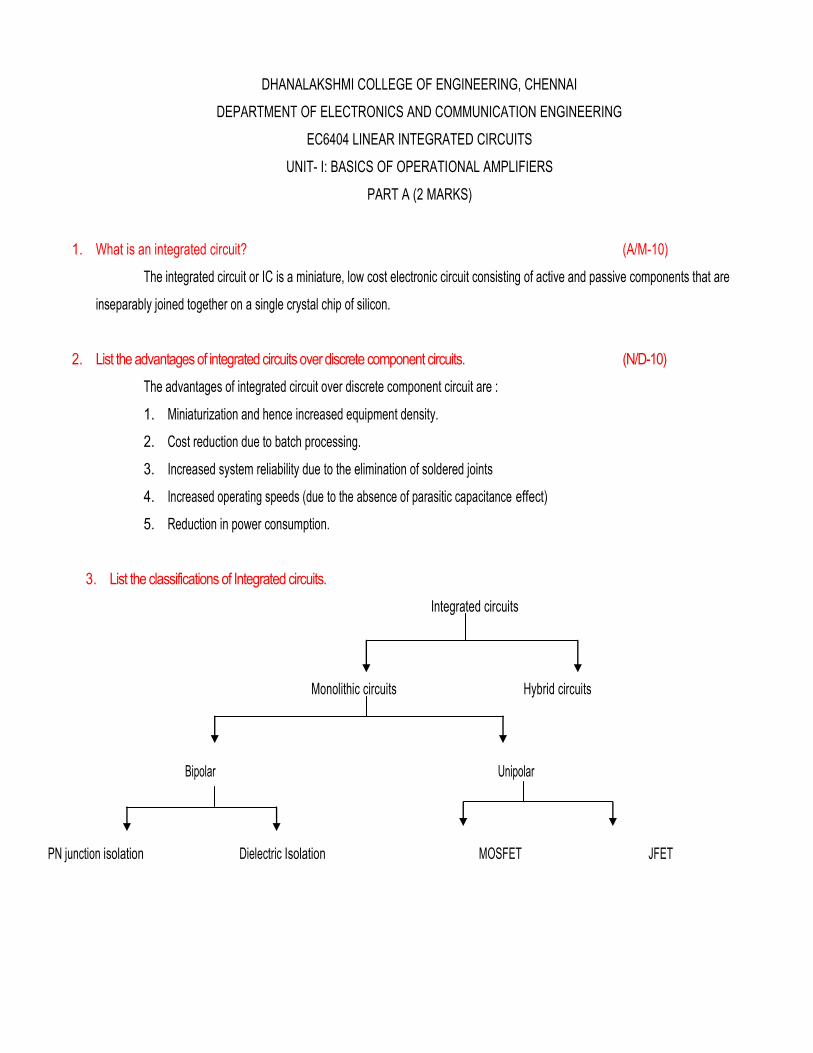
DHANALAKSHMI COLLEGE OF ENGINEERING, CHENNAI DEPARTMENT OF ELECTRONICS AND COMMUNICATION ENGINEERING EC6404 LINEAR INTEGRATED CIRCUITS UNIT- I: BASICS OF OPERATIONAL AMPLIFIERS PART A (2 MARKS) 1. What is an integrated circuit? (A/M-10) The integrated circuit or IC is a miniature, low cost electronic circuit consisting of active and passive components that are inseparably joined together on a single crystal chip of silicon. 2. List the advantages of integrated circuits over discrete component circuits. (N/D-10) The advantages of integrated circuit over discrete component circuit are : 1. Miniaturization and hence increased equipment density. 2. Cost reduction due to batch processing. 3. Increased system reliability due to the elimination of soldered joints 4. Increased operating speeds (due to the absence of parasitic capacitance effect) 5. Reduction in power consumption. 3. List the classifications of Integrated circuits. Integrated circuits Monolithic circuits Hybrid circuits Bipolar Unipolar PN junction isolation Dielectric Isolation MOSFET JFET
Transcript of DHANALAKSHMI COLLEGE OF ENGINEERING, · PDF file · 2017-01-25At high frequency,...
DHANALAKSHMI COLLEGE OF ENGINEERING, CHENNAI
DEPARTMENT OF ELECTRONICS AND COMMUNICATION ENGINEERING
EC6404 LINEAR INTEGRATED CIRCUITS
UNIT- I: BASICS OF OPERATIONAL AMPLIFIERS
PART A (2 MARKS)
1. What is an integrated circuit? (A/M-10)
The integrated circuit or IC is a miniature, low cost electronic circuit consisting of active and passive components that are
inseparably joined together on a single crystal chip of silicon.
2. List the advantages of integrated circuits over discrete component circuits. (N/D-10)
The advantages of integrated circuit over discrete component circuit are :
1. Miniaturization and hence increased equipment density.
2. Cost reduction due to batch processing.
3. Increased system reliability due to the elimination of soldered joints
4. Increased operating speeds (due to the absence of parasitic capacitance effect)
5. Reduction in power consumption.
3. List the classifications of Integrated circuits.
Integrated circuits
Monolithic circuits Hybrid circuits
Bipolar Unipolar
PN junction isolation Dielectric Isolation MOSFET JFET

4. What are the different methods available for fabrication of integrated resistors? (A/M-11)
The methods of fabrication of integrated resistors are
1. Diffused resistor
2. Epitaxial resistor
3. Pinched resistor
4. Thin film resistor
5. What is an ohmic contact?
Aluminium is used for making interconnections of a p-type impurity in silicon. The formation of rectifying p-n junction is
avoided by making n+ diffusions in the n-regions where contact is made using aluminum. Such contacts are called ohmic contacts.
6. List the limitations of monolithic ICs. (M/J-13)
The limitations of monolithic ICs are
1. The large value of resistances and capacitances cannot be formed by this type of ICs.
2. No method available to fabricate transformer or large values of inductors.
7. What is meant by ion implantation?
Ion implantation is an alternative to deposition diffusion and is used to produce a shallow surface region of do pant atom
deposited into a silicon wafer.
8. What is an operational amplifier?
An operational amplifier is a special type of amplifier that, by proper selection of its external components could be configu red for a variety
of operations such as amplification, addition, subtraction and integration.
9. Mention any four characteristics of an ideal operational amplifier. (N/D-12)
The Characteristics of an ideal operational amplifier are :
1. Open loop voltage gain AOL = ∞ (infinity)
2. Input impedanceRi=∞(infinity)
3. Output impedanceR o=0 (zero)
4. Zero offsetV0 =0 (zero)
5. Band widthBW = ∞ (infinity)
6.CMRR = ∞ (infinity)
7.Slew Rate = ∞ (infinity)

10. DefineSlew Rate(N/D-11)
1. Slew rate is defined as the maximum rate of change of output voltage caused by a step input voltage and is usually specified
in V/μs . Slew rate of 741 1C is 0.5 V/μs.
2. Slew rate can be defined as the maximum change of output voltage with respect to time.
11. What causes slew rate?
The rate at which the internal or external capacitance of an op-amp charges causes slew rate.
12. State the important features of instrumentation amplifier. (A/M-11)
The important features of instrumentation amplifier are
1. High gain accuracy
2. High CMRR
3. High gain stability with low temperature coefficient
4. Low dc offset
5. Low output impedance
13. Define– CMRR (A/M-11)
Common Mode Rejection Ratio (CMRR) is defined as the ratio of difference mode gain to common mode gain. Its ideal
value is infinity, and it is given by,
CMRR = | Ad| /|AC|
where Ad is difference mode gain and Ac is common mode gain.
14. Draw the internal block diagram of an op-amp circuit.
The internal block diagram of typical op-amp circuit is given below:
1. Differential amplifiers are used to provide high gain
2. The buffer is usually an emitter follower whose input impedanceis very high. It prevents loading of
high gain stage
3. The output driver is usually provided to give low output impedance
Vi Vo
Differential
Amplifier
Differential
Amplifier
Buffer and level
translator
Output
Driver

Part B (16 Marks)
1. (i) Define CMRR. Draw the circuit of an op-amp differential amplifier and write the expression for
CMRR. (8)
(ii) State Slew Rate. Explain the cause of slew rate and derive an expression for slew rate for an op-amp voltage
follower. (8) (M-10)
2. Explain the various processes involved in fabricating monolithic IC that integrates bipolar transistor, diode, capacitor
and resistor. (16) (M-10)
3. Explain the Widlar current source with circuit diagram and equation. (16) (N-11)
4. Explain the term epitaxy and epitaxial growth process. Also, explain the processing steps involved in the fabrication
of monolithic ICs. (16) (N-11)
5. Draw and explain the circuit of an instrumentation amplifier. Derive an equation for gain and prove how the desired
features are achieved. (16)
6. Explain the working of BJT – emitter coupled differential amplifier with neat diagram circuit diagram. Also explain
the concept of active load and with relevant circuit diagram. (16) (M-13)
7. State Full Power Bandwidth and Output Offset Voltage. Explain the different methods to nullify off- set voltage and
to improve slew rate. (16) (M-11)
8. Draw circuit diagram of the output stage of the IC 741 OP AMP, and explain its operation indicating the protection
mechanisms. (16) (N-10)
9. Explain the Wilson current source with circuit diagram and equations. (16)
10. Explain the practical Inverting amplifier and practical non-inverting amplifier with necessary equations.
(16)
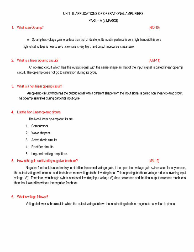
UNIT- II: APPLICATIONS OF OPERATIONAL AMPLIFIERS
PART – A (2 MARKS)
1. What is an Op-amp? (N/D-10)
An Op-amp has voltage gain to be less than that of ideal one. Its input impedance is very high, bandwidth is very
high ,offset voltage is near to zero , slew rate is very high, and output impedance is near zero.
2. What is a linear op-amp circuit? (A/M-11)
An op-amp circuit which has the output signal with the same shape as that of the input signal is called linear op-amp
circuit. The op-amp does not go to saturation during its cycle.
3. What is a non linear op-amp circuit?
An op-amp circuit which has the output signal with a different shape from the input signal is called non linear op-amp circuit.
The op-amp saturates during part of its input cycle.
4. List the Non Linear op-amp circuits.
The Non Linear op-amp circuits are:
1. Comparators
2. Wave shapers
3. Active diode circuits
4. Rectifier circuits
5. Log and antilog amplifiers.
5. How is the gain stabilized by negative feedback? (M/J-12)
Negative feedback is used mainly to stabilize the overall voltage gain. If the open loop voltage gain AOLincreases for any reason,
the output voltage will increase and feeds back more voltage to the inverting input. This opposing feedback voltage reduces inverting input
voltage V(-). Therefore even though AOLhas increased, inverting input voltage V(-) has decreased and the final output increases much less
than that it would be without the negative feedback.
6. What is voltage follower?
Voltage follower is the circuit in which the output voltage follows the input voltage both in magnitude as well as in phase.
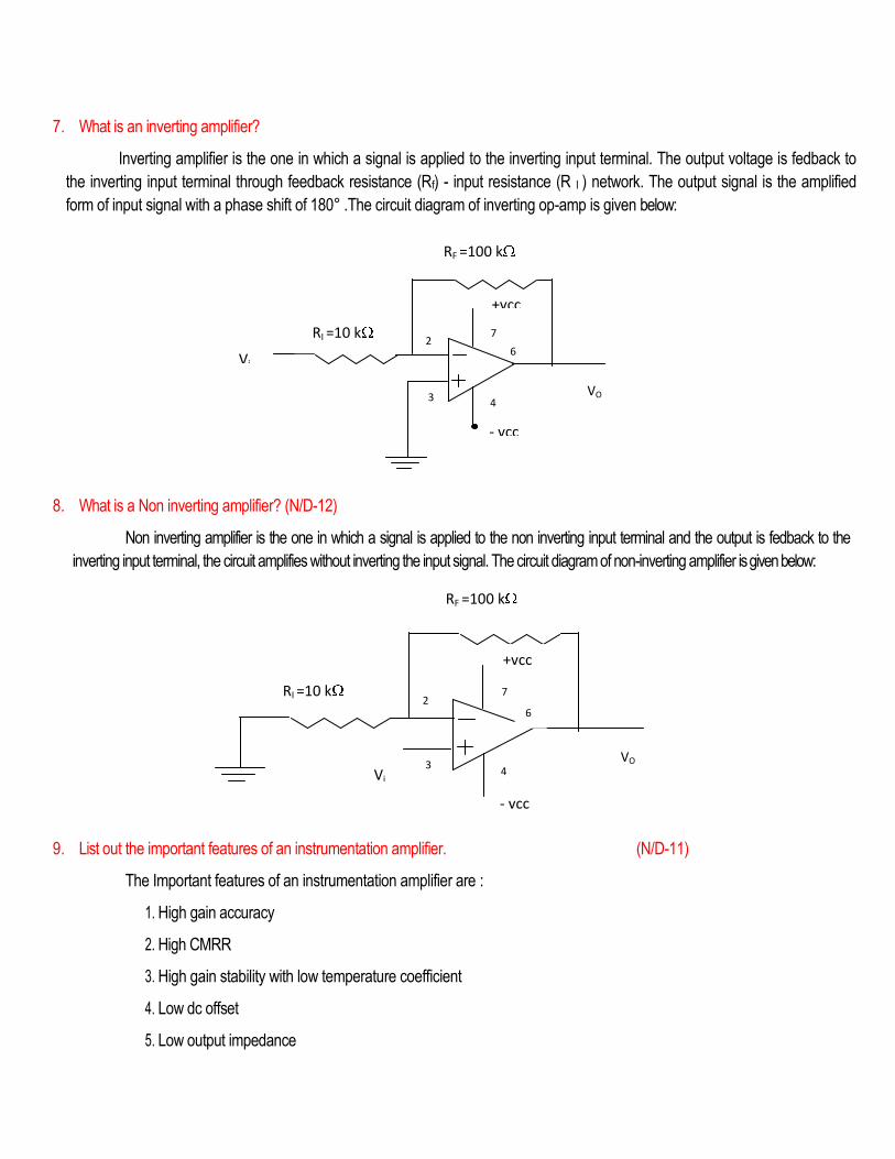
7. What is an inverting amplifier?
Inverting amplifier is the one in which a signal is applied to the inverting input terminal. The output voltage is fedback to
the inverting input terminal through feedback resistance (Rf) - input resistance (R I ) network. The output signal is the amplified
form of input signal with a phase shift of 180° .The circuit diagram of inverting op-amp is given below:
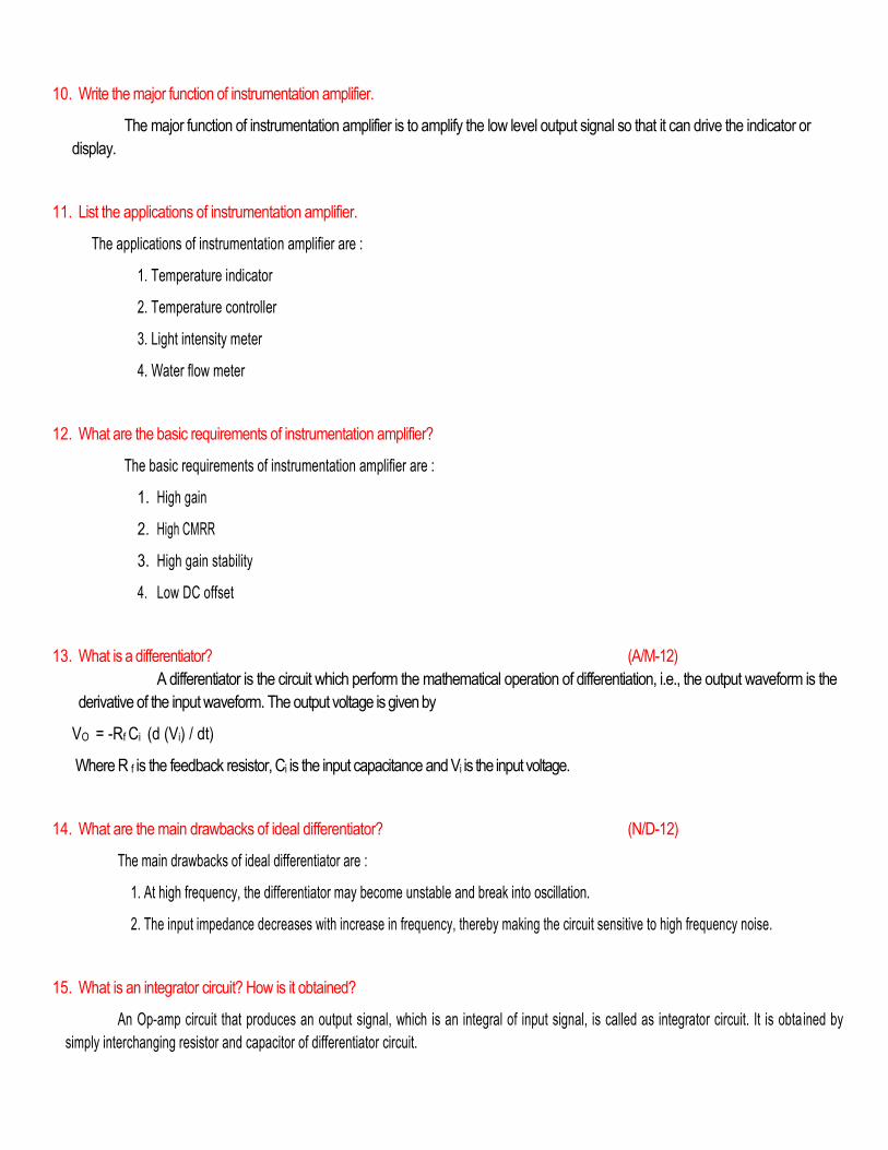
8. What is a Non inverting amplifier? (N/D-12)
Non inverting amplifier is the one in which a signal is applied to the non inverting input terminal and the output is fedback to the
inverting input terminal, the circuit amplifies without inverting the input signal. The circuit diagram of non-inverting amplifier is given below:
9. List out the important features of an instrumentation amplifier. (N/D-11)
The Important features of an instrumentation amplifier are :
1. High gain accuracy
2. High CMRR
3. High gain stability with low temperature coefficient
4. Low dc offset
5. Low output impedance
RF =100 k
VO
Vi
RI =10 k 7 2
+vcc
- vcc
6
3 4
VO
RF =100 k
+vcc
- vcc
6
3 4
Vi
RI =10 k 7 2
10. Write the major function of instrumentation amplifier.
The major function of instrumentation amplifier is to amplify the low level output signal so that it can drive the indicator or
display.
11. List the applications of instrumentation amplifier.
The applications of instrumentation amplifier are :
1. Temperature indicator
2. Temperature controller
3. Light intensity meter
4. Water flow meter
12. What are the basic requirements of instrumentation amplifier?
The basic requirements of instrumentation amplifier are :
1. High gain
2. High CMRR
3. High gain stability
4. Low DC offset
13. What is a differentiator? (A/M-12)
A differentiator is the circuit which perform the mathematical operation of differentiation, i.e., the output waveform is the
derivative of the input waveform. The output voltage is given by
VO = -Rf Ci (d (Vi) / dt)
Where R f is the feedback resistor, Ci is the input capacitance and Vi is the input voltage.
14. What are the main drawbacks of ideal differentiator? (N/D-12)
The main drawbacks of ideal differentiator are :
1. At high frequency, the differentiator may become unstable and break into oscillation.
2. The input impedance decreases with increase in frequency, thereby making the circuit sensitive to high frequency noise.
15. What is an integrator circuit? How is it obtained?
An Op-amp circuit that produces an output signal, which is an integral of input signal, is called as integrator circuit. It is obtained by
simply interchanging resistor and capacitor of differentiator circuit.
16. List the drawbacks of ideal integrator
The drawbacks of ideal integrator are
1. At low frequencies (dc), gain becomes infinity.
2. When the op-amp saturates i.e. the capacitor is fully charged, ideal integrator behaves like an open circuit.
17. Why is the practical integrator called as lossy integrator?
The gain of the integrator at lower frequencies can be limited to avoid the saturation problem, if the feedback capacitor C f is
shunted by a resistor R f .The parallel combination of R f and C f behaves like practical capacitor, which dissipates power, unlike an
ideal capacitor. For this reason, the circuit is called as lossy integrator.
18. List any four applications of practical Integrator
The applications of practical integrator are
1. Analog computers
2. Analog to digital computers
3. Wave shaping circuits
4. In ramp generators
19. Define - Frequency Scaling
Frequency Scaling is defined as the procedure used to convert an Original cut-off frequency f h to a new cut-off frequency
f h.
20. What is a comparator?
A comparator is a circuit which compares a signal voltage applied to one input of an op-amp with known reference
voltage at other input. It is basically an op-amp with output ± (Vsat).
21. What are the characteristics of the comparator? (A/M-13)
The important characteristics of the comparators are :
1. Speed of operation
2. Accuracy
3. Compatibility of the output

22. List the different types of comparator
The two types of comparators are
1. Inverting comparator
2. Non- Inverting comparator
23. List the applications of comparator
The applications of comparator are
1. Zero crossing detector
2. Window detector
3. Time marker generator
4. Phase meter
24. What is a Schmitt trigger?
A Schmitt trigger is an inverting comparator with positive feedback. It converts an irregular-shaped waveform to a square
wave or pulse, and is called as squaring circuit.

Part – B (16 Marks)
1. What is the need for an instrumentation amplifier? Analyze the same in detail. (16) (M-13)
2. Explain the operation of the Schmitt trigger. (16) (M-11)
3. Explainin detail the working of logarithmic and anti logarithmic amplifier (16)
4. Explain the operation of V to I and I to V converters. (8) (N-10)
5. With the circuit diagram,explain the second order Butterworth active low pass filter and derive an
expression for its transfer function. (16) (N-11)
6. Explain in detail the operation of the Differentiator. (8) (M-13)
7. Explain the operation of the positive clipper circuit and negative clipper circuit. (16)
8. With the circuit diagram explain the first order Butterworth active low pass filter and derive an
expression for its transfer function. (16) (N-09)
9. With the circuit diagram explain the first order Butterworth active high pass filter and derive an expression for its
transfer function. (8) (M-09)
10. With the circuit diagram explain the second order Butterworth active band pass filter and derive an
expression for its transfer function. (8) (N-12)
UNIT – III: ANALOG MULTIPLIER AND PLL
PART A (2 MARKS)
1. Why is VCO called as Voltage to Frequency (V – F) converter? (M/J-12)
A voltage controlled oscillator is an oscillator circuit in which the frequency of oscillations can be controlled by an
externally applied voltage (vc). The VCO provides the linear relationship between the applied voltage and the oscillation
of frequency. Hence VCO is called as Voltage to Frequency (V-F) converter.
2. Define - Capture range of a PLL. (N/D-11, M/J-10& N/D-03)
The range of frequency over which the PLL can acquire lock with an input signal is called capture range. The
PLL cannot acquire a signal outside the capture range, but once captured, it will hold on till the signal frequency goes
beyond the lock-in range. However, a large capture range will make PLL more susceptible to noise and undesirable
signal.
3. Define Voltage to Frequency Conversion factor. (N/D- 04 &M/J-11)
Voltage to frequency conversion factor kv is defined as the ratio of the frequency shift to the modulation voltage for
a VCO.
Kv = ∆fo / ∆vc
Here Kv is the modulation voltage required to produce the frequency shift ∆fo for a VCO.
4. What is compander? (N/D-06&A/M-10)
The peak signal is compressed at the transmitter and expanded at the receiver. This is called as companding. The
combination of a compressor and expander is called a compander.
5. Define - Lock-in range of a PLL. (M/J-10)
The range of frequencies over which the PLL can maintain lock with the incoming signal is called the lock-in range
or tracking range. It is expressed as a percentage of the VCO free running frequency fo.
6. Define FSK modulation. (M/J-10)
Frequency Shift Keying is a type of frequency modulation that the binary data or code is transmitted by means of a
carrier frequency that is shifted between two fixed frequency namely mark (logic1) and space frequency (logic 0).
7. What is an analog multiplier? (M/J-10)
A multiplier produces an output Vo, that is proportional to the product of two inputs V x and V y
Vo= k VxVy
where K is the scaling factor.
8. List the applications of PLL. (A/M-04 & N/D-09)
The applications of PLL are
a) Frequency multiplication and division
b) Frequency translation.
c) AM detection.
d) FM demodulation
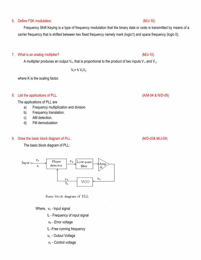
9. Draw the basic block diagram of PLL. (N/D-05& M/J-09)
The basic block diagram of PLL:
Where, vs - Input signal
fs - Frequency of input signal
ve - Error voltage
fo -Free running frequency
vo - Outout Voltage
vc - Control voltage
10. Mention some areas where PLL is widely used. (N/D-09)
PLL is widely used in
a) Radar synchronizations
b) Satellite communication systems
c) Air borne navigational systems
d) FM communication systems
e) Computers
11. What is a voltage-controlled oscillator? (A/M-04&A/M-10)
A voltage controlled oscillator is an oscillator circuit in which the frequency of oscillation can be controlled by an
externally applied voltage. It provides the linear relationship between the applied voltage and the oscillating frequency.
VCO is a free running multivibrator and operates at a set of frequency fo called free running frequency. This
frequency is determined by an external timing capacitor and an external resistor. It can also be shifted to either side by
applying a dc control voltage Vc to an appropriate terminal of the IC. The frequency deviation is directly proportional to
the dc control voltage and hence it is called a “Voltage Controlled Oscillator”.
12. What is FSK technique? (M/J-08)
In digital communication and computer peripheral, binary data is transmitted by means of a carrier frequency that is
shifted between two present frequencies. This type of data transmission is called Frequency Shift Keying (FSK)
technique.
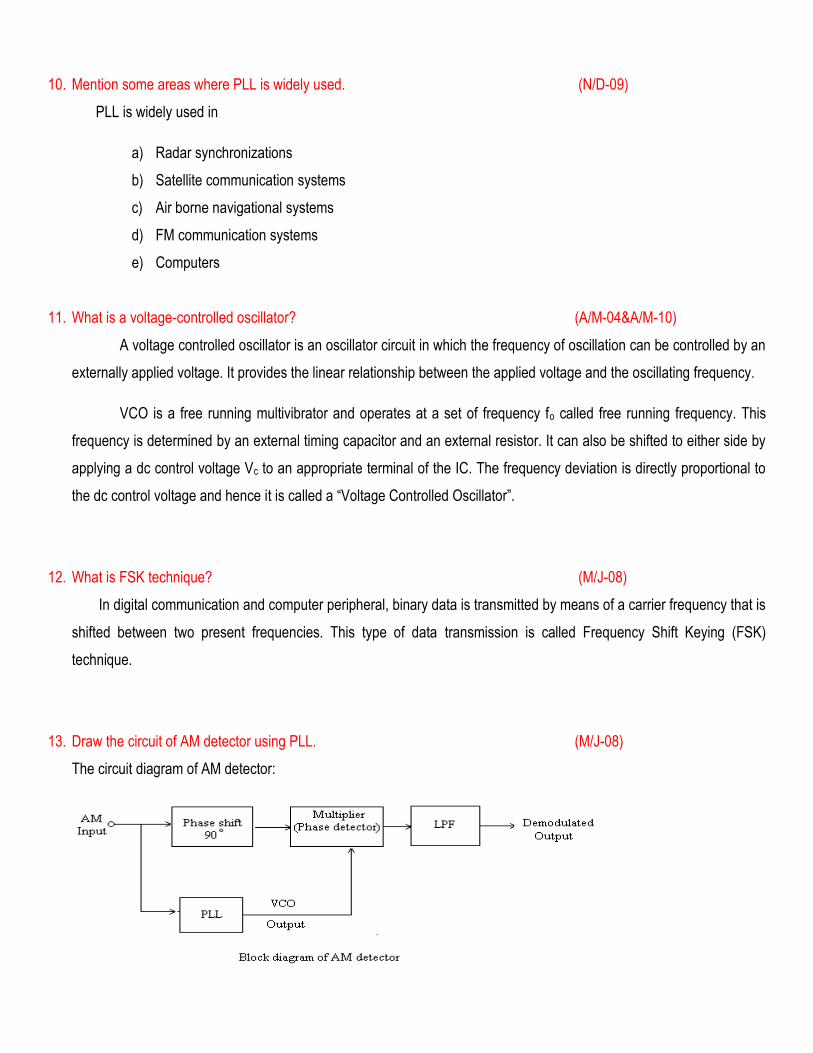
13. Draw the circuit of AM detector using PLL. (M/J-08)
The circuit diagram of AM detector:
14. What is an operational transconductance amplifier? Draw the schematic diagram. (N/D-07)
Transconductance amplifier is an operational amplifier circuit that converts the voltage input signal to a
proportional output current. There are two types of circuits possible.
a. V-I convertor with floating load
b. V-I convertor with grounded load
15. What are the essential building blocks of a PLL? (A/M- 10–R2004)(M-07)
The essential building blocks of PLL are
a. Phase detector
b. Low-pass filter
c. Amplifier
d. Voltage Controlled Oscillator
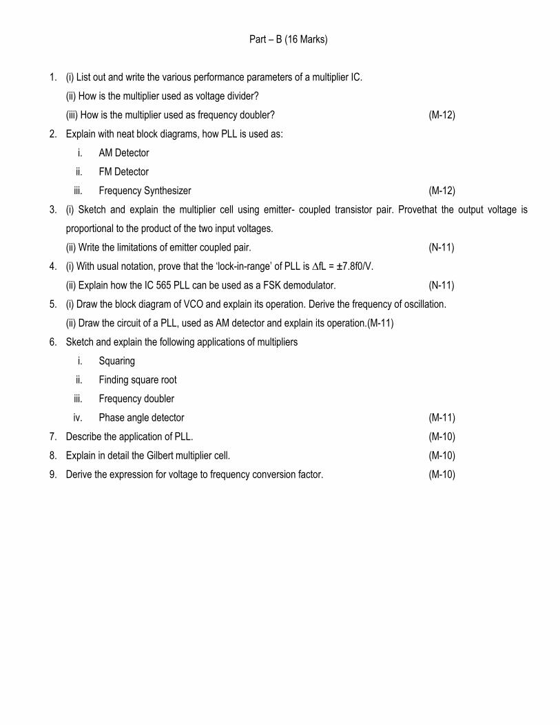
16. Draw the block diagram of a multiplier using log and antilog amplifiers. (M/J-06 &N/D-07)
The block diagram of a multiplier:
Part – B (16 Marks)
1. (i) List out and write the various performance parameters of a multiplier IC.
(ii) How is the multiplier used as voltage divider?
(iii) How is the multiplier used as frequency doubler? (M-12)
2. Explain with neat block diagrams, how PLL is used as:
i. AM Detector
ii. FM Detector
iii. Frequency Synthesizer (M-12)
3. (i) Sketch and explain the multiplier cell using emitter- coupled transistor pair. Provethat the output voltage is
proportional to the product of the two input voltages.
(ii) Write the limitations of emitter coupled pair. (N-11)
4. (i) With usual notation, prove that the „lock-in-range‟ of PLL is ∆fL = ±7.8f0/V.
(ii) Explain how the IC 565 PLL can be used as a FSK demodulator. (N-11)
5. (i) Draw the block diagram of VCO and explain its operation. Derive the frequency of oscillation.
(ii) Draw the circuit of a PLL, used as AM detector and explain its operation.(M-11)
6. Sketch and explain the following applications of multipliers
i. Squaring
ii. Finding square root
iii. Frequency doubler
iv. Phase angle detector (M-11)
7. Describe the application of PLL. (M-10)
8. Explain in detail the Gilbert multiplier cell. (M-10)
9. Derive the expression for voltage to frequency conversion factor. (M-10)

UNIT – IV ANALOG TO DIGITAL AND DIGITAL TO ANALOG CONVERTERS
PART A (2 MARKS)
1. Why is flash ADC called as the fastest ADC? (ND-09, M/J-11&N/D-11)
The flash type ADC circuit has the advantage of high speed, as the conversion take place simultaneously rather
than sequentially. The typical conversion time of this circuit is 100 ns or less.
2. Define - Accuracy of a D/A converter (M/J-10&M/J-11)
Absolute accuracy is the maximum deviation between the actual converter output and the ideal converter output.
Relative accuracy is the maximum deviation after gain and offset errors have been removed. Data sheets normally
specify relative accuracy rather than absolute accuracy. The accuracy of a converter is also specified in terms of LSB
increments or percentage of full scale voltage.
3. Define - Settling time of D/A converter (M/J-11)
The settling time of DAC represents the time it takes for the output to settle within a specified band (±1/2) LSB of its
final value following a code change at the input. It depends upon the switching time of the logic circuitry due to internal
parasitic capacitances and inductances. Settling time ranges from 100ns to 10µs depending on word length and type of
circuit used.
4. Define - Resolution of a data converter (A/M-03, 05, 06 & 07,N/D-10 & N/D-11)
The resolution of a converter is the smallest change in voltage that may be produced at the output or input of the
converter.
The resolution of an ADC is defined as the smallest change in analog input for a one bit change at the output.
5. Name the essential parts of a DAC. (M/J-10)
The essential parts of a DAC are
a) Drive motors
b) Analog devices
c) Deglitcher
d) Filter
6. An 8 bit successive approximation ADC is driven by a 1 MHz clock. Find its conversion time. (A/M-10)
Solution:
The time taken for one clock pulse is 1 µs
Tc = T(n+1)
Where,
Tc – Conversion time
n – number of bits
Tc = 1x10⁻⁶(8+1)
Tc = 9µsec.
7. List the advantages of integrating type ADC. (A/M-10)
The advantages of integrating type ADC are
a) Integrating type ADC do not need a sample and hold circuit at the input.
b) It is possible to transmit frequency even in noisy environment or in an isolation form.
c) Used for precision measurement of slow varying signal.
d) It is immune to temperature caused variations in R1 and C1.
e) Highly accurate and low cost.
8. Which is the fastest ADC and why? (M/J-10& N/D-10)
Flash type A/D converter is the fastest ADC.
The flash type ADC circuit has the advantage of high speed as the conversion take place simultaneously rather
than sequentially. The typical conversion time of this circuit is 100 ns or less.
9. Compare and Contrast binary ladder and R-2R ladder DAC. (N/D-10)
S.No. Binary ladder R-2R ladder
1. Wide range of resistor values is required. Easy to build accurately with two metal film resistors.

2. It is impracticable to fabricate large value of resistor
Easy to fabricate.
3. Finite resistance of the switches disturbs the binary weighted relationship among the various currents.
Voltage remains constant with changing input binary words.
10. List the applications of NE565. (N/D-10)
The applications of NE565 are
a) Frequency multiplier
b) Frequency synthesizer
c) FM detector
d) FSK demodulator
e) Frequency translator
11. What are the advantages and disadvantages of R-2R ladder DAC? (M/J-10)
The advantages of R-2R ladder DAC are
a) Easier to build
b) Number of bits can be expanded by adding more sections.
The disadvantages of R-2R ladder DAC are
a) More power dissipation makes heating that in turns develops non-linear ties in DAC.
12. List the disadvantages of flash type A/D converter. (M/J-10)
The disadvantages of flash type A/D converter are
a) The simultaneous type A/D converter (flash type A/D converter) is not suitable for A/D conversion with more than 3
or 4 digital output bits.
b) The number of comparators required are (2n-1) where n is the desired no of bits. Hence the number of comparators
approximately doubles for each added bit.
13. What are the advantages of dual slope ADC? (N/D-09)
The advantages of dual slope ADC are
a) Dual slope ADC provides excellent noise rejection of ac signals whose periods are integral multiples
of the integration time T.
b) Dual slope ADC are particularly suitable for accurate measurement of slowly varying.
Eg: Thermocouples and weighing scales.

14. List the direct type ADCs. (N/D-09) The direct type ADCs
a) Flash (comparator) type converter
b) Counter type converter
c) Tracking or servo converter
d) Successive approximation type converter
Part – B (16 Marks)
1. (i) Explain the following types of electronic switches used in D/A converter with suitable diagrams.
a) Totem pole MOSFET switch
b) CMOS inverter as a switch
(ii) Explain the working of R-2R ladder DAC, by taking example of a 3-bit DAC circuit. Sketch the corresponding
equivalent circuits and hence obtain the equation for output. (M-12)
2. (i) With a neat circuit diagram and wave form of output, explain the working of Dual slope A/D converter.
(ii) Construct a table of comparison of Flash, Dual-slope and successive approximation ADCs in terms of
parameters such as speed, accuracy, resolution and input-hold-time. (M-12)
3. Explain the following types of digital to analog converters, with suitable circuit diagrams:
(i) Binary weighted resistors DAC
(ii) R-2R Ladder DAC
(iii) Inverted R-2R Ladder DAC (N-11)
4. (i) Draw the circuit of a flash type ADC and explain its operation in detail.
(ii) What is the purpose of high speed sample and hold circuit? Sketch such a circuit and explain. Also write the
parameters associated with it. (N-11)
5. (i) Explain in detail the successive approximation type A/D converter with the neat block diagram.
(ii)Explain the over sampling A/D converter with functional block diagram. (M-11)
6. (i) Explain the operation of a weighted resistor type D/A converter.
(ii) What are the limitation of a weighted resistor type D/A converter? (M-11)
UNIT – V: WAVEFORM GENERATORS AND SPECIAL FUNCTION ICs
PART A (2 MARKS)
1. What are the limitations of IC 723 general purpose regulator? (N/D-12)
The limitations of 1C 723 voltage regulators are :
i) No built in thermal protection
ii) It has no short circuit current limits
2. What is power amplifier? (N/D-12)
The amplifiers which are used to deliver large power to the load in the range of few watts and which handle
large signals to produce large power is called power amplifiers or large signal amplifiers.
3. What are the limitations of three terminal regulator? (M/J-12)
The 3 pin regulators have the following limitations:
i) There is no short circuit protection. ii) The output positive and negative voltage is fixed.
4. What is a switched capacitor filter? Mention its applications. (M/J-12, N/D-10,M/J-09)
A switched capacitor filter is a three terminal device, which consists of capacitors, periodic switches and operational
amplifier whose open circuit voltage transfer characteristics represents filtering characteristics.
5. State the applications of 555 timer IC. (N/D-13)
The applications of 1C 555 timer are :
i) Oscillator
ii) Pulse generator
iii) Ramp and square wave genrator
iv) Monoshot multivibrator
v) Burglar alarm
vi) Traffic light control and
vii) Voltage monitor.
6. Define line regulation with respect to a voltage regulator. (N/D-13)
Line regulation is defined as the percentage change in the output voltage for a change in the input (line) voltage. It is
usually expressed in milli volts.
Line regulation = VHL- VLL
where VHL= load voltage with high line voltage.
VNL= load voltage with low line voltage.
7. Write the formula for a period of oscillations in an op-amp astable circuit. (M/J-13)
Period of oscillations in an op-amp astable circuit is
T= 2RCln (Vsat+VT/ Vsat - VT
8. Define duty cycle of a periodic pulse waveform. (M/J-13)
9. Define the duty cycle in astable multivibrator using IC 555. (N/D-11,A/M-11)
The duty cycle is given by
For an astable multivibrator
Therefore adjusting RA , and RB the duty cycle of an astable multivibrator can be varied.
10. What are the advantages of Switched capacitor filter over active filters? (N/D-11)
The advantages of Switched capacitor filter over active filters are
i) Low system cost
ii) Low exterenal component count
iii) High accuracy
iv) Excellent temperature stability
v)
11. What is an optocoupler? Mention its applications. (A/M-11)
A combination of LED and photodiode is called as an optocoupler. This device can couple the input signal to
the output circuit.
Opto coupler can be used as a coupler between any two stages for better electrical isolation.
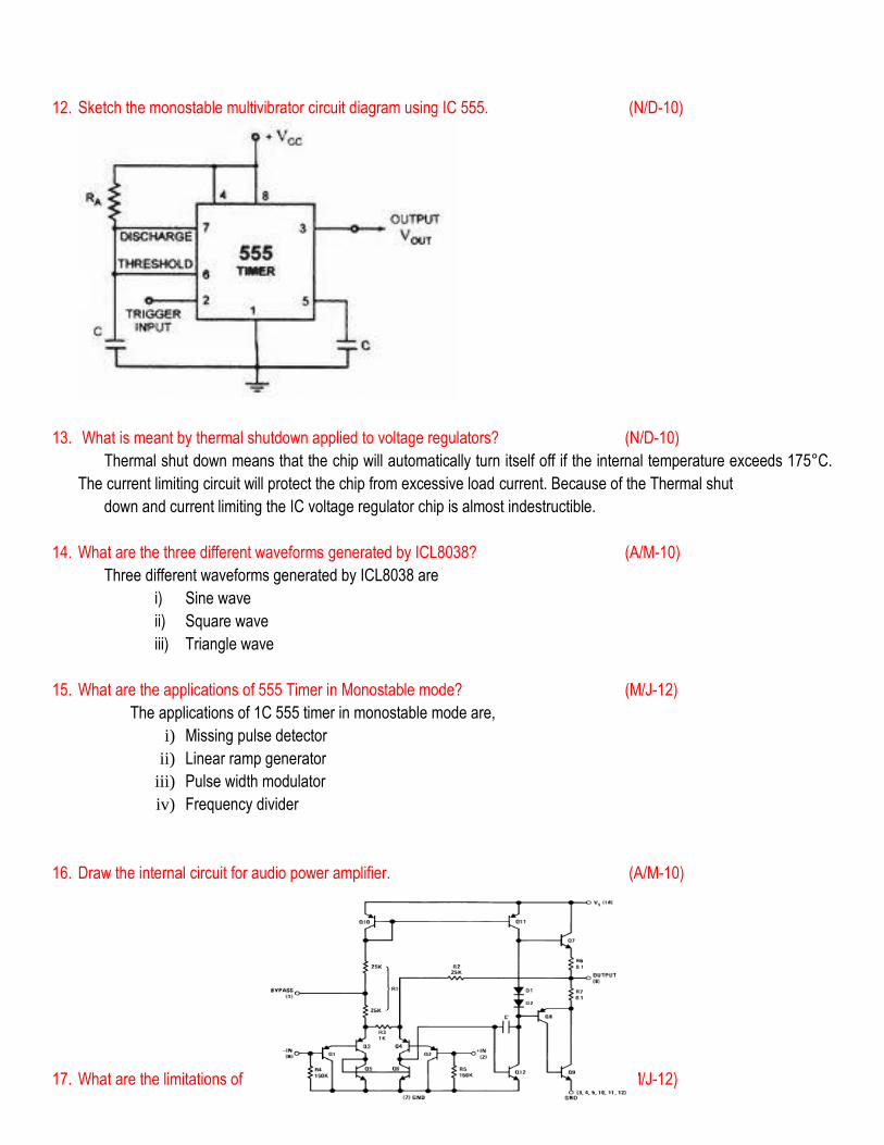
12. Sketch the monostable multivibrator circuit diagram using IC 555. (N/D-10)
13. What is meant by thermal shutdown applied to voltage regulators? (N/D-10)
Thermal shut down means that the chip will automatically turn itself off if the internal temperature exceeds 175°C.
The current limiting circuit will protect the chip from excessive load current. Because of the Thermal shut
down and current limiting the IC voltage regulator chip is almost indestructible.
14. What are the three different waveforms generated by ICL8038? (A/M-10)
Three different waveforms generated by ICL8038 are
i) Sine wave
ii) Square wave
iii) Triangle wave
15. What are the applications of 555 Timer in Monostable mode? (M/J-12)
The applications of 1C 555 timer in monostable mode are,
i) Missing pulse detector
ii) Linear ramp generator
iii) Pulse width modulator
iv) Frequency divider
16. Draw the internal circuit for audio power amplifier. (A/M-10)
17. What are the limitations of linear voltage regulators? (M/J-12)

The limitations of linear voltage regulators
i) The required input step down transformer is bulky and expensive
ii) Due to low line frequency (50 Hz), the large values of filter capacitors are required
iii) The efficiency is very low
iv) Input must be greater than the output voltage
v) As large is the difference between input and output voltage more is the power dissipation in the series pass
transistor
vi) For higher input voltages efficiency decreases
vii) The need for dual supply is not economical and feasible to achieve with the help of linear
regulators
18. What are the basic blocks of 555 timers? (A/M-11) The basic blocks of 555 timers are
i) A relaxation oscillator ii) R-S flip- flop iii) Two comparators iv) Discharge transistor
19. Give two advantages of an isolation Amplifier. (A/M-10)
Advantages of isolation Amplifiers are i) Small size ii) Low offset iii) Low drift iv) Wide bandwidth v)Ultra low leakage vi) Low leakage
20. Draw the switched capacitor version of an Integrator. (A/M-10)
21. What is an isolation amplifier? (N/D-09)
An isolation amplifier is an amplifier that offers an ohmic or electrical isolation between its input and output
terminals.
22. Define SMPS. (N/D-09)
A switched-mode power supply (switching-mode power supply, SMPS, or switcher) is
an electronic power supply that incorporates a switching regulator to convert electrical power efficiently.
23. What are the requirements for designing a video amplifier? (M/J-09)
The requirements for designing a video amplifier are
i) To increase the bandwidth the gain must be reduced by decreasing RL
ii) The load capacitance should be as small as possible
iii) If discrete circuit is used choose the transistor having high value of fT and low value of base spreading
resistor rbb‟
iv) Use CE-CB cascade pair as an amplifier because of its high frequency is better than the CE amplifier
v) Use one or more negative feedback loops ti increase the bandwidth of the amplifier
24. Name two applications of an isolation amplifier. (N/D-08)
Applications of an isolation amplifiers are
i) Low level signals with high common-mode voltages
ii) Breaking ground loops
iii) Medical patient monitoring equipment
iv) Protection of electronic instruments/equipment
v) Analog and Digital acquisition
vi) Industrial environment
25. List the characteristics of optocoupler. (A/M-08)
The characteristics of an optocoupler are:
i. Current intensity ratio
ii. Isolation impedance
iii. Response time
iv. CMRR
v. Bandwidth

Part – B (16 MARKS)
1. Sketch the functional block diagram of the following and explain their working principle: (M-12)
i. (i) IC 555 Timer. (8)
ii. (ii) General purpose voltage regulation IC 723. (8)
2. Explain the working principle of isolation amplifier with neat diagram. (8) (M-12)
3. Explain the principle of operation of opto couplerswith neat diagram. (8) (M-12)
4. i) Explain the working of monostablemultivibrator. (14) (N-13)
ii) What are opto-couplers?(2) (N-13)
5. i) Explain the working of a general purpose voltage regulator. (14) (N-13)
ii) What is the need for isolation amplifiers?(2) (N-13)
6. Explain the working of IC 555 in astable modewith the neat functional block diagram. (8) (N-11)
7. Describe in detail, the working principle of IC 8038 function generator. (8) (N-11)
8. Explain the operation of LM 380 power amplifier with a neat functional diagram. (8) (N-11)
9. Explain the operation of switched capacitor filter. What are the advantages and dis-advantages of this type of filter?
(8) (N-11)