DFM and SMT Assembly Guideline - PC Components
29
TB-2082 DFM and SMT Assembly Guideline Revision “C“ Specification Revision Status Revision SCR No. Description Initial Date “-“ 33277 Initial Release J. Marvin 1/16/01 “A” 36994 Update stencil design, JEDEC tray info, add weight table & GenRad ref, delete AirVac detail. J. Proulx 10/19/01 “B” 39831 Revised in it’s entirety and reformatted. J. Proulx 9/17/02 “C” 42921 Clarify board warp req, add stand-off req, change handling to reflect new packaging, changes to paste process – add selection matrix, reflow process – additional thermal probe and plug note, and reflow verification and de-bug. J. Proulx 8/13/03 Teradyne, Inc. VHDM is a registered trademark of Teradyne, Inc. VHDM-HSD, NeXLev, and Connection Systems Division GbX are trademarks of Teradyne, Inc. While the information in this document 44 Simon Street is reliable at the time of publication, it is subject to change without notice. Nashua, NH 03060 603.879.3000 Copyright © Teradyne, Inc. 2002 • All rights reserved www.teradyne.com/tcs
Transcript of DFM and SMT Assembly Guideline - PC Components

TB-2082
DFM and SMT Assembly Guideline
Revision “C“
Specification Revision Status
Revision SCR No. Description Initial Date “-“ 33277 Initial Release J. Marvin 1/16/01 “A” 36994 Update stencil design, JEDEC tray info, add weight
table & GenRad ref, delete AirVac detail. J. Proulx 10/19/01
“B” 39831 Revised in it’s entirety and reformatted. J. Proulx 9/17/02 “C” 42921 Clarify board warp req, add stand-off req, change
handling to reflect new packaging, changes to paste process – add selection matrix, reflow process – additional thermal probe and plug note, and reflow verification and de-bug.
J. Proulx 8/13/03
Teradyne, Inc. VHDM is a registered trademark of Teradyne, Inc. VHDM-HSD, NeXLev, and Connection Systems Division GbX are trademarks of Teradyne, Inc. While the information in this document 44 Simon Street is reliable at the time of publication, it is subject to change without notice. Nashua, NH 03060 603.879.3000 Copyright © Teradyne, Inc. 2002 • All rights reserved www.teradyne.com/tcs

DFM and SMT Assembly Guideline TB-2082 Revision “C“ Table of Contents
1.0 DFM Guideline Introduction 1.1 Scope 1.2 Purpose 1.3 Reference Documents
1.3.1 Customer Use Drawings
2.0 Design Introduction – NeXLev Connector
3.0 Design Requirements 3.1 NeXLev Solder Joint Definition – Reliability Factors 3.2 Landing Pad Footprint 3.3 PCB General Requirements and Suggested Routing 3.4 Connector Float Allowance and PCB Fabrication Tolerances 3.5 Layout and Orientation for Multi-Connector Applications 3.6 Mechanical Requirements - Standoffs 3.7 Keep-out Zone and Clearances – Connector height < 10.5mm 3.8 Keep-out Zone and Clearances – Multi Connector and Connector height > 15.5mm
4.0 Manufacturing Introduction
4.1 Connector Inspection
5.0 Connector Handling
6.0 Solder Paste Process
7.0 Placement Process 7.1 Placement Alignment – “Best-Fit” 7.2 Placement - 15.5 and 23.5mm Receptacles 7.3 Feeders 7.4 JEDEC Tray Set-up
8.0 Reflow Process
8.1 Reflow Process – Detailed Verification and De-bug 8.2 Vacuum “Pick-up” Cap Removal
9.0 Double Sided Reflow Process
10.0 Rework Process
Addendums:
A. NeXLev Connector Weights B. NeXLev DFM Check Sheet - used for design reviews, and process start-up.
Copyright © Teradyne, Inc. 2002 • All rights reserved Page 2 of 29
DFM and SMT Assembly Guideline TB-2082 Revision “C“ 1.0 DFM Guideline Introduction
This document is intended to provide design criteria and process information that will promote
automation, cost and cycle time reduction, and help to produce designs that will yield high quality for the solder attach of NeXLev connectors. The NeXLev connector will be used in many assembly processes, and because all processes are different, this document provides a starting point, or “baseline” criteria for application process development. This document is not intended to be the final process definition, nor is it intended to constrain designs. If customers cannot meet/follow all of the recommendations, they should contact TCS to discuss the best alternatives.
1.1 Scope
This document has been prepared to communicate the application guidelines for the NeXLev Surface Mount Connector. It provides Printed Circuit Board (PCB) footprint and layout criteria, and “starting-point” process recommendations for SMT assembly. Updates and revisions will be issued on a continuous basis to expand the guidelines, address changes in technology and manufacturing capabilities, and cover modifications and/or additions to current criteria.
1.2 Purpose
DFM is the sharing of manufacturing guidelines developed from industry standards and the knowledge gained from design and production. Applying these guidelines concurrently, in new product development with the design and application of Teradyne’s NeXLev connector, can positively impact cost, time to market, and quality of the end product.
1.3 Reference Documents
Located at: http://www.teradyne.com/prods/tcs/products/hpi/NeXLev/drawings.html
1.3.1 Customer Use Drawings C-471-1025-500 Plug (drawing for application) C-470-1075-500 Receptacle (drawing for application) 471-1025-500 Plug (drawing for inspection) 470-1075-500 Receptacle (drawing for inspection)
1.4 Levels of Requirement
For each requirement, an impact and benefit statement is included to quantify the requirement. Some requirements are stated as being recommended or preferred per the following:
Recommended: The minimum processing requirement – a deviation will most likely impact manufacturability and cost.
Preferred: Should be done when possible – a deviation could impact manufacturability and cost.
Copyright © Teradyne, Inc. 2002 • All rights reserved Page 3 of 29

DFM and SMT Assembly Guideline TB-2082 Revision “C“ 2.0 Design Introduction – NeXLev Connector
The NeXLev connector is a wafer construction organized in a 10-row by up to 30 columns of
signal contacts, with each signal wafer having integral strip-line shielding. This wafer construction allows for the contacts to be spaced on a 1.5mm x 1.75mm grid. The connector can be specified in separation heights ranging from 10mm to 30mm.
The connector is a completely SMT attach, utilizing ball grid technology for termination to the board. Designed with solder joint reliability in mind, the connector has a mechanically compliant structure, and is readily applied using standard SMT processes. Standard versions of the NeXLev connector contain either 10, 20 or 30 wafers. (100, 200, or 300 positions)
The connector is different than a standard BGA device, due to the compliant structure, which has a .76 mm (30 Mil) eutectic ball, re-flowed on the end of a formed pedestal.
One wafer contains 10 signal and 9 ground
balls and the connector is provided in 10, 20, and 30 wafer configurations.
Ball is attached to a pedestal at the end of the “S-Bend” Compliant Lead
Ground Shield
S-Bend Compliant Lead
Copyright © Teradyne, Inc. 2002 • All rights reserved Page 4 of 29
DFM and SMT Assembly Guideline TB-2082 Revision “C“ 3.0 Design Requirements
3.1 NeXLev Solder Joint Definition – Reliability Factors The recommendations made below have a direct impact on the reliability of the NeXLev solder joint,
and play an important role in facilitating the connectors' ability to self-center and achieve the best possible location tolerances. This is especially important when multiple connectors are being used.
Requirements DFM Impact/Benefit
• Recommend using a “Copper Defined” landing pad as opposed to a “Solder-Mask Defined” pad.
• “Copper defined” better insures a round, accurately located pad – critical to part location tolerance.
• “Copper defined” pad produces a more reliable solder joint – allowing solder to wrap around the pad edge.
• Pad Size = .60mm (.024”) • Smaller pad will result in decreased ball-to-pad angle, based on solder volume – increasing the risk of solder fracture.
• Larger pads will increase the risk of shorting.
• Solder mask should be clear around pad • In-accurate registration will result in solder mask encroaching onto copper pad.
S-Bend Compliant Lead
Copper Pad
Solder Mask
Copper defined pad yields highest quality solder joint – compared to Solder Mask defined: - Doesn’t inhibit connectors ability to self-center - Solder wraps around pad edge - maximum strength
Solder mask is clear around pad
PCB
Angle is critical to solder joint reliability – a smaller pad will result in a fatter ball, decreasing angle and creating weak points in the joint
Copyright © Teradyne, Inc. 2002 • All rights reserved Page 5 of 29

DFM and SMT Assembly Guideline TB-2082 Revision “C“
3.2 Landing Pad Footprint Refer to customer drawings, C-471-1025-500 Plug and C-470-1075-500 Receptacle, for overall landing
pad layout. See below for the detail of a single pad and via design. The exact landing pad and via design will depend on several factors including design goals, routability, customer specific design for manufacturability (DFM) guidelines, and PCB fabricator capabilities. The diagram below offers a starting point, with the critical parameters in bold.
Requirements DFM Impact/Benefit/Alternatives
• Teradyne recommends a .60mm (.024”) “Copper Defined” landing pad over a “Solder-Mask Defined” pad.
• See previous section for impact
• Minimum .22mm (.009”) Solder Mask Dam between pad and via.
• Prevents solder from wicking away from pad and into via, causing insufficient solder joints.
• It’s preferred to mask the vias if design allows, or if a .22mm min dam can’t be held.
• Via drill sizes can be changed based on PCB fabricators board thickness aspect ratio, but must insure a minimum solder mask dam.
∅ 0.64mm (0.025”) Via Pad and inner pad diameter
Board Pad and Via Detailed Footprint ∅ 0.34mm (0.0135”) Drill diameter
– Dependant on fab shop aspect ratio capability
Exposed Solder-able surface
∅ 0.44mm (0.017”) Via solder mask aperture (Component Side) ∅ 0.63mm (0.025”)(Via Pad Side) Note: Eliminate this aperture if minimum dam can’t be achieved
0.70mm (0.028”)
0.30mm (0.012”) 0.22mm (0.009”)
Minimum Dam* Note: Solder Mask Dam Is maximized using a “D” shaped aperture
∅ 0.70mm (0.028”) Pad Solder Mask Aperture (Insure that mask is clear of Pad)*
∅ 0.60mm (0.024”) Pad Diameter
*Note: Insure PCB Fabricators solder mask registration capabilities
Copyright © Teradyne, Inc. 2002 • All rights reserved Page 6 of 29

DFM and SMT Assembly Guideline TB-2082 Revision “C“
3.3 PCB General Requirements and Routing Example The NeXLev connector can be routed from one side using five layers - each with two 6 mil traces with a
7 mil space. Routing from both sides may further reduce the layer count. The following pattern shows a “Serpentine” trace pattern, and this routing pattern can be achieved using the exact pad and via footprint stated previously. The diagram below is an example of a possible starting point.
Requirements DFM Impact/Benefit
• Maximum recommended board warp – 7 mils/inch*. (Sufficient for surface finishes that have less than .001” thickness variation such as OSP, ENIG, Immersion Tin and Silver.)
• Minimizes the risk of opens
• Preferred maximum board warp - 5 mils/inch*. (May be required if using a HASL surface finish)
• Minimizes the risk of opens while allowing for other variables such as solder paste height and pad flatness*.
*Note: The recommended board warp is also based on the assembly process stencil thickness used. For more detail, see selection matrix in section 6.0 – “Solder Paste Process”
Copyright © Teradyne, Inc. 2002 • All rights reserved Page 7 of 29
Example – Differential Routing: Shows a 6-mil trace with a 7-mil space, in a “serpentine” pattern allowing for two runs. *Note: the runs are parallel to the wafer – providing the most routing space.
Landing Pad Layout Connector Side
Trace Routing Details

DFM and SMT Assembly Guideline TB-2082 Revision “C“
3.4 Connector Float Allowance and PCB Fabrication Tolerances The NeXLev connector is designed to accommodate SMT assembly and PCB fabrication tolerances.
Below are the total allowances for the connector design, and the recommended PCB fabrication tolerances.
Total Connector Float Allowance
Silkscreen outline – visible after component placement.
+/- 0.20mm Max error from nominal location
+/- 0.10mm Max error from nominal location
X,Y TP < 0.10 mmFrom “Datum Point”
Assume this connector footprint center to be the
“Datum Point”
Recommended PCB Footprint True Position Tolerance
Copyright © Teradyne, Inc. 2002 • All rights reserved Page 8 of 29
DFM and SMT Assembly Guideline TB-2082 Revision “C“
3.5 Layout and Orientation for Multi-Connector Applications
Layout: Requirements DFM Impact/Benefit
• Preferred to align connectors in the same direction • Ease of multi-board mating alignment
• Connectors are parallel across the larger span, and in series on shorter spans.
• Maximizes designed-in “float” tolerances
• Max span is dependant on board fabrication tolerances – reference section 3.4.
• Board tolerance exceeds connector max alignment tolerance.
• Layout should include a slightly larger silkscreen outline of the component housing.
• Silkscreen is visible after connector placement, and allows for “first-piece” visual inspection of polarity/orientation.
Connectors are placed in same orientation
Connectors are not placed in same orientation
Preferred Not preferred Mating and Un-Mating:
Preferred Preferred Acceptable Not Recommended Copyright © Teradyne, Inc. 2002 • All rights reserved Page 9 of 29

DFM and SMT Assembly Guideline TB-2082 Revision “C“
3.6 Mechanical Requirements
Standoffs: Requirements DFM Impact/Benefit
• Provide sufficient hold down forces to retain mated cards.
• Insure connectors stay mated during shipment and vibration.
• Standoffs are preferred for single mated pair applications. Customers that decide against the use of stand-offs will need to verify that the forces due to assembly weight, assembly flexing caused by handling, shipping and vibration shock (g), do not exceed NeXLev un-mating forces*.
• Maintain minimum wipe regardless of shock and vibration.
• Standoffs are recommended for applications with greater than one mated pair.
• Maintain minimum wipe regardless of shock, vibration and board warp tolerances
• PCB holes for standoff fasteners must permit a true position misalignment of .20mm and an angular displacement of .05 degrees minimum (Board-to-board fastening must comply to the connector alignment)
• Allows connector to act as the primary alignment feature of mated boards
• Prevents stresses to connector and/or printed circuit board
• Stand-off lengths are determined by referring to the “NeXLev Stacking Height Tolerance Matrix” found on the website – see reference below**
• Matrix provides mated stack heights with tolerances – selecting the correct stand-off length minimizes board or connector stresses.
• Stand-offs should be placed outside the connector keep-out zones. See following sections for detail.
• Allows for connector rework without having to remove stand-offs
*NeXLev un-mating forces are generally 20% less than mating forces. (Forces will decrease as mating cycles increase) **NeXLev Stacking Height Tolerance Matrix: http://www.teradyne.com/prods/tcs/docs/techbull/nexlev_stacking_height_tolerances.pdf
Copyright © Teradyne, Inc. 2002 • All rights reserved Page 10 of 29

DFM and SMT Assembly Guideline TB-2082 Revision “C“
3.7 Keep-out Zone and Clearances – Connector height < 10.5mm The NeXLev connector keep-out zone is required for re-work capability. This allows clearance around
the connector housing for rework tooling and nozzles.
Requirements DFM Impact/Benefit • The recommended minimum clearance required is
3mm – preferred clearance is 4mm to non-fragile adjacent components.
• Rework nozzle - physical clearance
• It’s preferred to have 5mm clearance to adjacent devices that are very fine pitch with small thermal mass, and could re-reflow – this is dependent on board thickness, copper weight and NeXLev height
• Prevents re-reflow of adjacent device, which could cause shorts/defects on that device.
Non-Fragile Devices – Leaded - 50 mil pitch,
chips, etc.
4mm Preferred clearance to Non-fragile devices
3mm Minimum - physical clearance for rework nozzle
Top Side
Bottom Side
Fragile Devices – Micro BGA, CGA,
Leaded Fine Pitch, etc.
Rework Nozzle
5mm Preferred clearance to fragile devices
Copyright © Teradyne, Inc. 2002 • All rights reserved Page 11 of 29

DFM and SMT Assembly Guideline TB-2082 Revision “C“
3.8 Keep-out Zone and Clearances – Multi Connector and Connector heights > 15.5mm This NeXLev connector keep-out zone is required for re-work capability of taller devices with taller adjacent
components.
Requirements DFM Impact/Benefit • Preferred to have 5mm clearance between
tall, > 15.5mm NeXLev connectors, or, to other surrounding components of similar height.
• Allow room/clearance for site cleaning and preparation, and manual paste application using micro stencil.
• Prevents re-reflow of adjacent device, which could cause shorts/defects on that device.
• Eliminates the need for reflow shielding of smaller thermal mass components
Tall adjacent components
5mm Preferred clearance between tall components
Top Side
Bottom Side
Fragile Device – Micro BGA, CGA, Leaded
Fine Pitch, etc.
5mm minimum preferred clearance to fragile devices
Copyright © Teradyne, Inc. 2002 • All rights reserved Page 12 of 29

DFM and SMT Assembly Guideline TB-2082 Revision “C“ 4.0 Manufacturing Introduction – NeXLev Connector
The NeXLev connector is a wafer construction organized in a 10-row by up to 30 columns of
signal contacts, with each signal wafer having integral strip line shielding. This wafer construction allows for the contacts to be spaced on a 1.5mm x 1.75mm grid. The connector can be specified in separation heights ranging from 10mm to 30mm.
The connector is a completely SMT attach, utilizing ball grid technology for termination to the board. Designed with solder joint reliability in mind, the connector has a mechanically compliant structure and is readily applied using standard SMT processes. Standard versions of the NeXLev connector contain either 10, 20 or 30 wafers. (100, 200 or 300 positions)
The connector is different than a standard BGA device, due to the compliant structure, which has a .76 mm (30 Mil) eutectic ball, re-flowed on the end of a formed pedestal. The compliant structure requires that the connectors be handled with more care than a standard BGA
device. The connector is not as fragile as a fine-pitch leaded device, but does require some of the pre-cautions. Improper handling can bend the compliant lead and result in ball locations outside of true position tolerances.
Ball is attached to a pedestal at the end of the “S-Bend” Compliant Lead
One wafer contains 10 signal and 9 ground balls and the connector is provided in 10, 20, and 30 wafer configurations.
Ground Shield
S-Bend Compliant Lead
Copyright © Teradyne, Inc. 2002 • All rights reserved Page 13 of 29

DFM and SMT Assembly Guideline TB-2082 Revision “C“
4.1 Connector Inspection
NeXLev connectors are 100% laser inspected before leaving Teradyne. Each ball is laser scanned and checked for radial true position, co-planarity and minimum ball-to-ball spacing. This is done using an automated 3-D laser inspection system.
Requirements DFM Impact/Benefit
• Visual inspection is not suggested. • Requires manual handling of part – removal/replacement from JEDEC tray, if not done carefully, can cause lead damage
• Visual inspection is inherently inaccurate due to the subjective nature.
• Incapable of determining ball position accuracy to a best-fit grid.
• Parts/JEDEC tray should be removed from packing material and the JEDEC tray placed directly onto the placement machine.
• Eliminates manual handling
Example: Picture of connector shown when you visually inspect the balls by tipping the part at an angle – ball appears out of position.
Why is visual inspection inherently inaccurate?
Copyright © Teradyne, Inc. 2002 • All rights reserved Page 14 of 29

DFM and SMT Assembly Guideline TB-2082 Revision “C“
4.1 Connector Inspection – cont’d
This shows what the above connector looks like when looking straight at the ball field. If the ball is compared to it’s neighbors, it appears to be out of spec.
Note: This is a picture of the connector placed on a glass template using a best-fit placement algorithm. The black circles represent the footprint pads.
However, when ball positions are accurately determined, and then compared to the best-fit grid, the ball position is not out of spec. The ball position differences are split - minimizing the variation.
* This is the ball that was visually determined to be a problem.
Copyright © Teradyne, Inc. 2002 • All rights reserved Page 15 of 29

DFM and SMT Assembly Guideline TB-2082 Revision “C“ 5.0 Connector Handling
The NeXLev connector is an assembly, with the solder balls attached to leaded pedestals, and is thus more susceptible to handling damage than a standard BGA device.
Requirements DFM Impact/Benefit
• Connectors should be kept in the original packaging until they’re used.
• Protects the ball field until it can be loaded into the placement machine
• Once the assembly run is complete, tray should be removed from machine, placed back into the bottom pan, replace top cover, and Velcro strap together – as shown below. (For more detail refer to TB-2121)
• Protection of ball field.
• It is not necessary to bag and re-vacuum seal* the tray, if the parts are used within a reasonable time frame for eutectic solder balls – shelf life is dependent on stockroom environmental conditions.
• NeXLev Connector materials are not moisture sensitive, and do not require pre-bake.
• Place tray flat on rack for storage or transport – don’t place on edge.
• Prevents parts from moving out of tray slot, and potentially bending leads, which support the solder balls.
• SMT operators should minimize the handling of the part that could cause bent leads, such as moving parts around in the JEDEC tray, removing from sticky tape during program verification, placing the part on a workbench with the ball field down, etc.
• Minimizes bent leads, true position problems, and post reflow shorting.
Partially loaded tray
Two Velcro straps
located as shown. Molded Top Cover Bottom Pan and JEDEC Tray
Copyright © Teradyne, Inc. 2002 • All rights reserved Page 16 of 29

DFM and SMT Assembly Guideline TB-2082 Revision “C“ 6.0 Solder Paste Process
Requirements DFM Impact/Benefit • Liquid Photo-Imageable (LPI) solder mask
over bare copper is preferred. • Most common – provides best adhesion for solder
mask - preventing peeling and flaking of mask during assembly processes.
• Preferred to use a 6 mil stencil (Minimum stencil thickness of 5 mil)* • Minimizes the risk of opens
• Recommended to use a reduced aperture - .021” • Minimizes the risk of shorting
*A 5 mil stencil thickness can be used, but requires either a .005”/inch board warp spec, or a .001” pad co planarity spec on surface finish thickness variability. (HASL finishes can exceed this limitation.) Board Warp Matrix - The following matrix defines the board warp spec required for each of the listed
variables – Stencil Thickness and Pad Finish Co-planarity
Pad Finish Co-planarity
<.001” <.002”
5 mil +2/-0 mil .007” .005”
5 mil +2/-.5 mil .005” Not Recommended 6 mil +2/-0 mils .007” .007”
Stencil Thickness and Paste Process
Variation 6 mil +2/-.5 mil .007” .005”
Copyright © Teradyne, Inc. 2002 • All rights reserved Page 17 of 29
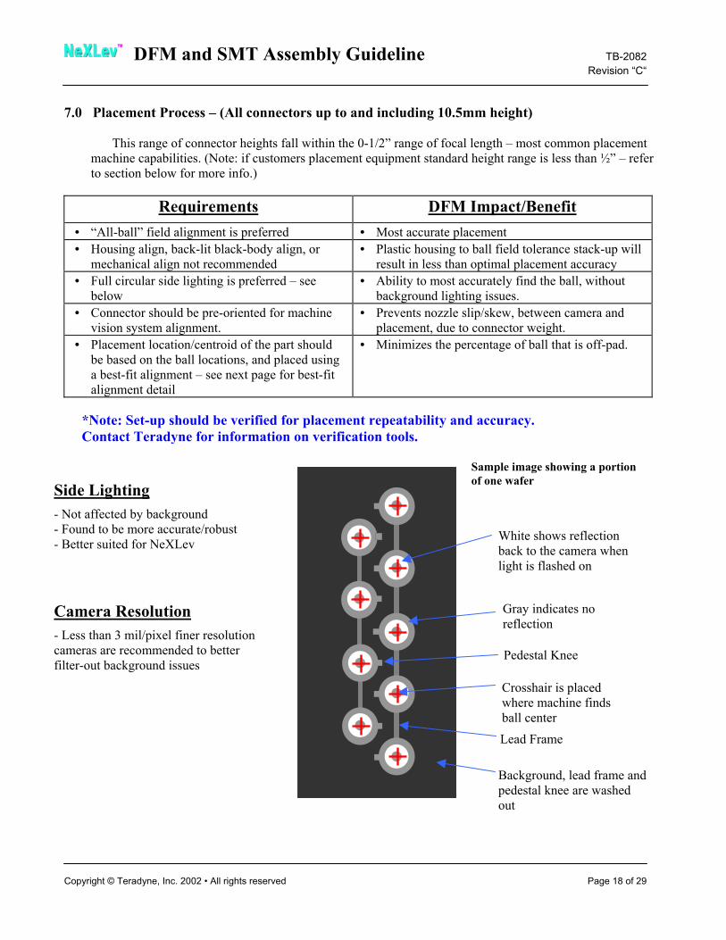
DFM and SMT Assembly Guideline TB-2082 Revision “C“ 7.0 Placement Process – (All connectors up to and including 10.5mm height)
This range of connector heights fall within the 0-1/2” range of focal length – most common placement
machine capabilities. (Note: if customers placement equipment standard height range is less than ½” – refer to section below for more info.)
Requirements DFM Impact/Benefit
• “All-ball” field alignment is preferred • Most accurate placement • Housing align, back-lit black-body align, or
mechanical align not recommended • Plastic housing to ball field tolerance stack-up will
result in less than optimal placement accuracy • Full circular side lighting is preferred – see
below • Ability to most accurately find the ball, without
background lighting issues. • Connector should be pre-oriented for machine
vision system alignment. • Prevents nozzle slip/skew, between camera and
placement, due to connector weight. • Placement location/centroid of the part should
be based on the ball locations, and placed using a best-fit alignment – see next page for best-fit alignment detail
• Minimizes the percentage of ball that is off-pad.
*Note: Set-up should be verified for placement repeatability and accuracy. Contact Teradyne for information on verification tools.
Sample image showing a portion of one wafer
Side Lighting - Not affected by background - Found to be more accurate/robust - Better suited for NeXLev White shows reflection
back to the camera when light is flashed on
Camera Resolution - Less than 3 mil/pixel finer resolution cameras are recommended to better filter-out background issues
Gray indicates no reflection
Pedestal Knee
Crosshair is placed where machine finds ball center
Lead Frame Background, lead frame and
pedestal knee are washed out
Copyright © Teradyne, Inc. 2002 • All rights reserved Page 18 of 29

DFM and SMT Assembly Guideline TB-2082 Revision “C“
7.1 Placement Alignment – “Best-Fit” Ball positional tolerances are greater for NeXLev than standard BGA devices, due to the wafer
construction and S-bend compliant design. This variation in ball location requires the use of a “best-fit” placement algorithm to minimize the percentage of ball that is off-pad. See examples below for detail.
The best-fit placement splits the difference
Placement Comparison
The worse case solder balls are less than 25% off pad.
“Best-Fit”
This is an example of a placement where the overall
resulting solder ball alignment variation is minimized using a
best-fit placement.
Board Pad
Solder Ball
Shorting risk is high on signal balls
First row of balls are centered.
Fixed End Row
This is an example of the same part with a placement that uses
only the first row of balls to determine placement location.
Copyright © Teradyne, Inc. 2002 • All rights reserved Page 19 of 29

DFM and SMT Assembly Guideline TB-2082 Revision “C“
7.2 Placement Process – 15.5 and 23.5mm Receptacles* These connector heights exceed the 1/2” maximum height for most common placement machines, and
have the same requirements as the 0-1/2” range with the following added restrictions.
Requirements DFM Impact/Benefit • Shortened “custom” nozzle may be required.
(Refer to placement machine specs for more info)
• Part can be presented within the camera’s focal plane, avoid part interferences with machine conveyor, board sensors, and placement head hardware
• Specific placement order and connector location on board assembly may be required.
• Avoid interference of previously placed part, as the placement head moves across the board to place a second part.
• Large bore nozzle is required for maximum vacuum force – placements should be verified to insure correct nozzle selection.
• Connector should be pre-oriented for machine vision system alignment.
• Prevents nozzle slip/skew, between camera and
placement, due to connector weight.
*Contact Teradyne for more detailed SMT application instructions on taller NeXLev connectors
Copyright © Teradyne, Inc. 2002 • All rights reserved Page 20 of 29

DFM and SMT Assembly Guideline TB-2082 Revision “C“
7.3 Placement Process – Feeders
Requirements DFM Impact/Benefit
• Connectors are shipped in standard JEDEC outline trays and are equipped with a cap that provides a flat vacuum surface – see below and next page.
• Meets the requirements of industry standard placement equipment
• The caps can be removed by hand after reflow • See reflow process section for more info • There are six different tray sizes –
(3) Plug: 10, 20 and 30 wafer lengths. (3) Receptacle: 10, 20 and 30 wafer lengths.
• The only size variation in the trays are slots that hold the connector. Overall tray length and width are standard. See next page.
• Trays should be loaded into machine with the “tray-notch” in the upper left hand corner - for both the plug and receptacles. See diagram next page.
• Allows for part set-up standardization across the product line.
• Consistent loading of all parts minimizes the risk of reversed loading of the tray into the placement machine.
• Plug trays are blue, Receptacle trays are black • Minimizes the risk of reversed loading of the part into the tray.
• Minimizes the risk of putting the wrong part in the wrong tray.
Plug Receptacle
Plug Receptacle
Vacuum CapVacuum Cap
Copyright © Teradyne, Inc. 2002 • All rights reserved Page 21 of 29

DFM and SMT Assembly Guideline TB-2082 Revision “C“
7.4 Placement Process - JEDEC Tray Set-up Dimension “A” Dimension “B” "C" Dimension “Z”* Tray Part #
471-1025-100 23.63 29.75 9 14.95 801-2225-000 471-2025-100 30.53 50.75 5 14.95 801-2226-000 471-3025-100 35.30 61.10 4 14.95 801-2227-000 471-1045-100 23.63 29.75 9 16.95 801-2225-000 471-2045-100 30.53 50.75 5 16.95 801-2226-000 471-3045-100 35.30 61.10 4 16.95 801-2227-000 471-1065-100 23.63 29.75 9 18.95 801-2225-000 471-2065-100 30.53 50.75 5 18.95 801-2226-000 471-3065-100 35.30 61.10 4 18.95 801-2227-000 470-1075-100 23.63 29.75 9 13.95 801-2228-000 470-2075-100 30.53 50.75 5 13.95 801-2229-000 470-3075-100 35.30 61.10 4 13.95 801-2230-000 470-1105-100 23.63 29.75 9 16.95 801-2228-000 470-2105-100 30.53 50.75 5 16.95 801-2229-000 470-3105-100 35.30 61.10 4 16.95 801-2230-000 470-1155-100 23.63 29.75 9 21.95 801-2228-000 470-2155-100 30.53 50.75 5 21.95 801-2229-000 470-2155-100 35.30 61.10 4 21.95 801-2230-000 470-1235-100 23.63 29.75 9 29.95 801-2228-000 470-2235-100 30.53 50.75 5 29.95 801-2229-000 470-3235-100 35.30 61.10 4 29.95 801-2230-000
* “Z” is the height from the bottom of the tray to the top of the vacuum “pick-up” cap
(3.8) 315.00
135.90
“C” = # of “B” spaces “B” “A”
25.95
(3X) 28.00
JEDEC Tray With 30-Wafer Connectors – shown for reference (Dimensions are in mm)
Tray Notch
Into Placement Machine
Copyright © Teradyne, Inc. 2002 • All rights reserved Page 22 of 29

DFM and SMT Assembly Guideline TB-2082 Revision “C“ 8.0 Reflow Process
Requirements DFM Impact/Benefit
• To determine correct oven settings, follow standard reflow profile processes for set-up and placement of thermal probes.
• Insure even heat distribution across the part.
• Locate one thermal probe on top of the connector housing during reflow profiling – It is preferred to keep the plastic below 260°C with a max allowable temperature of 280°C.
• Insures against plastic over-heating and damage.
• Locate at least (2) thermal probes – one on an outer ball, and one on an inner ball – may require drilling through the board
• Insures balanced reflow profile definition for all of the solder joints.
• Set process to the solder paste vendor’s recommended profile.
• This varies by the chemical make-up of each solder paste, and also varies from one paste vendor to the next.
• After first-side reflow process, inspect connector to insure that housing is seated to the board surface – see below.
• This insures good reflow and balls have completely collapsed. Unseated connectors are due to improperly reflowed balls, and could result in long-term reliability failures.
Note: NeXLev plugs are more commonly profiled incorrectly. The housing is open, and the plug wafer construction transfers heat more readily than the receptacle. The plug ball-field can get to reflow temperatures much quicker than the board. This thermal differential may require the lower oven heaters to be set hotter than the upper heaters, providing thermal balance between the board and connector.
Locate one thermal probe on inner ball (Primarily required for larger receptacle connectors
and may require drilling through board)
Locate one thermal probe on outer ball
Locate one thermal probe on housing
NeXLev Assembled to PCB After First Reflow
Connector housing is seated to PCB
PCB
Copyright © Teradyne, Inc. 2002 • All rights reserved Page 23 of 29

DFM and SMT Assembly Guideline TB-2082 Revision “C“
8.1 Reflow Process – Detailed Verification and De-bug Below is the recommended method for process debug or 100% verification of process set-up and
establishing the best profile. (This method is destructive and requires the use of a solder sample) • Inspect connector to insure that the housing has completely settled to the board surface • Pry the housing from the board surface using a sharp edge - wedged between the housing and board
surface – pry the ends only. Insure wedge doesn’t go too deep and catch a wafer. • Housing will break away from wafers at heat-staked joint.
• Solder joints are exposed to allow 100% visual inspection
• Spread wafers to reveal ball field • Lift housing off wafers parallel to the board surface
Pry Point
Pry Points
Copyright © Teradyne, Inc. 2002 • All rights reserved Page 24 of 29

DFM and SMT Assembly Guideline TB-2082 Revision “C“
8.2 Reflow Process – Vacuum “Pick-up” Cap Removal
Requirements DFM Impact/Benefit • Post reflow vacuum cap removal • Vacuum cap can be removed after reflow/inspection.
(Note: A new vacuum cap is required for connector rework)
• Remove cap as shown in Figure 1 for the Plug, and Figure 2 for the receptacle.
• By pulling the cap straight up from the connector, the housing shell could be damaged, and separate from the wafers
2
1
2
11. Push cap to one side Figure 1 Plug
2. Peel cap up
2
1
2Figure 2
Receptacle 1
1. Push cap to one side
2. Peel cap away.
Copyright © Teradyne, Inc. 2002 • All rights reserved Page 25 of 29

DFM and SMT Assembly Guideline TB-2082 Revision “C“ 9.0 Double Sided Reflow Process
Because of the surface tension forces created by a NeXLev solder joint, the majority of connector sizes can run upside down in a double sided reflow process.
Requirements DFM Impact/Benefit • The majority of the connectors can run upside
down in a double-sided reflow process. • Surface tension forces of the solder joint are greater
than the weight/ball forces.
• Preferred to run the heavier* NexLev connectors through the 2nd pass of a double-sided reflow process.
• Prevents the need to run heavier devices through reflow upside down – minimizing the risk of the connector falling off or sagging away from the board.
• Before running connectors upside down, inspect connector to insure that housing is seated to the board surface – see Reflow Process section for more info.
• Improperly seated connectors indicate incorrect reflow and possible cold and/or insufficient solder joints, therefore reducing the surface tension forces required to hold the part on the board.
* Refer to Addendum “A” for more detailed information on weight/ball by part number. All connector sizes up to, and including 10.5 mm tall, should not be an issue. However, because every assembly process is not the same, the customer may want to verify this in their process. The 15.5 and 23.5 mm receptacles will require specific testing for each process and design application, because the weight/ball is close to the allowable limits of calculated surface tension forces. Note: The final decision to run NexLev connectors upside down, without any secondary method of retention, is with the customer. For more information on possible methods of retention – contact Teradyne.
Copyright © Teradyne, Inc. 2002 • All rights reserved Page 26 of 29

DFM and SMT Assembly Guideline TB-2082 Revision “C“ 10.0 Rework Process
The rework of a NeXLev connector, for solder shorts and opens, requires that the connector be
completely removed and replaced with a new connector.
Requirements DFM Impact/Benefit • Use specialized BGA rework equipment for connector
removal and replacement, and should include thermal profiling and temperature measurement capability.
• Achieves an all-ball reflow at point of removal without excessive heat to the connector and PCB, or insufficient heat causing lifted pads.
• Locate one thermal probe on top of the connector housing during reflow profiling – It is preferred to keep the plastic below 260°C with a max allowable temperature of 280°C.
• Insures against plastic over-heating and damage. (See reflow section for more detail.)
• Placement location/centroid of the part should be based on the ball locations, and placed using a best-fit alignment – see next page for best-fit alignment detail
• Minimizes the percentage of ball that is off-pad.
• Semi-Automated placement capability is preferred – including vacuum pick-up and placement.
• This will provide consistent placements.
• Split Vision alignment systems are required to allow a ball-field best-fit alignment to PCB footprint.
• Allows blind alignment of ball to pad - minimizing placement error.
• Hand/Manual placement is not recommended. • Manual placement is inconsistent, and blind/housing align does not provide the required placement accuracy.
• Using custom NeXLev nozzles is preferred for the taller receptacles (15.5 and 23.5 mm)
• Because of the higher thermal masses, more consistent/even heat distribution is required.
• Follow normal rework processes for PCB site cleaning and prep, and reflow profile development.
• Improves rework yield and insures reliable solder joints
• “Flux-only” processing is not recommended. • Inconsistent amount of metal left on pad during site prep, resulting in excessive pad co-planarity variation – increased risk of solder opens.
• Paste deposition is recommended using either an automated dispensing system or manual micro stencils – resulting in a 6 mil tall x 21 mil diameter deposit.
• Prevents opens/shorts with high reliability solder joints.
• Re-balling of NeXLev connectors is not recommended. • Re-balling processes not available for NeXLev.
The most popular rework systems, which have NeXLev custom nozzles, and have also developed a full process for all the different sizes, include Air-Vac and SRT. For more info go to the following Web Sites:
Air-Vac http://www.air-vac-eng.com/nozzleconnector.htm SRT http://www.teradyne.com/prods/cbt/products/rework/prod_rework.html
Copyright © Teradyne, Inc. 2002 • All rights reserved Page 27 of 29

DFM and SMT Assembly Guideline TB-2082 Revision “C“ Addendum “A”
NeXLev Connector Weights
TCS p/n Description
# of solder balls
Weight, without cap
(grams)
Weight/ball, without cap
(grams)
Weight, with cap(grams)
Weight/ballwith cap (grams)
4701075100 7,5mm NeXLev RCPT, 100 posn 190 4.0 0.0211 4.6 0.0242 4701105100 10,5mm NeXLev RCPT, 100 posn 190 6.0 0.0316 6.6 0.0347 4701155100 15,5mm NeXLev RCPT, 100 posn 190 8.0 0.0421 8.6 0.0453 4701235100 23,5mm NeXLev RCPT, 100 posn 190 12.0 0.0632 12.6 0.0663 4702075100 7,5mm NeXLev RCPT, 200 posn 380 6.0 0.0158 6.6 0.0174 4702105100 10,5mm NeXLev RCPT, 200 posn 380 10.0 0.0263 10.6 0.0279 4702155100 15,5mm NeXLev RCPT, 200 posn 380 14.0 0.0368 14.6 0.0384 4702235100 23,5mm NeXLev RCPT, 200 posn 380 23.1 0.0608 23.7 0.0624 4703075100 7,5mm NeXLev RCPT, 300 posn 570 8.0 0.0140 8.6 0.0151 4703105100 10,5mm NeXLev RCPT, 300 posn 570 13.1 0.0230 13.7 0.0240 4703155100 15,5mm NeXLev RCPT, 300 posn 570 21.0 0.0368 21.6 0.0379 4703235100 23,5mm NeXLev RCPT, 300 posn 570 33.7 0.0591 34.3 0.0602 4711025100 2,5mm NeXLev PLUG, 100 posn 190 4.0 0.0211 4.6 0.0242 4711045100 4,5mm NeXLev PLUG, 100 posn 190 4.5 0.0237 5.1 0.0268 4711065100 6,5mm NeXLev PLUG, 100 posn 190 6.0 0.0316 6.6 0.0347 4712025100 2,5mm NeXLev PLUG, 200 posn 380 6.0 0.0158 6.6 0.0174 4712045100 4,5mm NeXLev PLUG, 200 posn 380 8.3 0.0218 8.9 0.0234 4712065100 6,5mm NeXLev PLUG, 200 posn 380 10.0 0.0263 10.6 0.0279 4713025100 2,5mm NeXLev PLUG, 300 posn 570 8.0 0.0140 8.6 0.0151 4713045100 4,5mm NeXLev PLUG, 300 posn 570 12.2 0.0214 12.8 0.0225 4713065100 6,5mm NeXLev PLUG, 300 posn 570 16.0 0.0281 16.6 0.0291
Note: cap refers to vacuum pickup cap
Copyright © Teradyne, Inc. 2002 • All rights reserved Page 28 of 29

DFM and SMT Assembly Guideline TB-2082 Revision “C“
Copyright © Teradyne, Inc. 2002 • All rights reserved Page 29 of 29
Addendum “B”: DFM and Assembly Readiness Check Sheet
Item Sect Check Change/Comments Who Status 3.1 • Copper defined .60mm (024”) pad – clear of solder mask 3.2 • Minimum .22mm (.009”) Solder Mask dam to Via, or via
masking
3.3/6.0 • Specify board warp spec per process variables • Multi connector orientation is the same • Long side of connector is parallel across the larger spans
PCB Design
3.4/ 3.5
• Layout includes slightly oversized silkscreen outline of connector.
Inspection 4.1 • Manual component inspection not recommended • Removal/replacement from JEDEC tray is not
recommended – minimize manual handling Handling 4.0/
5.0 • Handling process should include re-packaging and
handling pre-cautions.
6.0 • Stencil thickness is 6 mils – 5-mil thickness is acceptable. Solder Paste • Stencil aperture should be 21 mils
7.0 • Set-up should include ball-field align, full circular side lighting, and pre-orient align.
7.1 • Best-Fit placement is required
Placement
7.2 • Custom programming and nozzles may be required for the taller connectors.
• Follow solder paste manufacturer’s recommended profile.
8.0
• When profiling, include thermal probe attachment to the top of housing, to insure against plastic over-heating.
Reflow
8.1 • Follow recommended process for vacuum cap removal. 9.0 • All connectors up to and including 10.5mm tall, may
require verification in specific process. Double
Sided Reflow • 15.5 and 23.5 will require verification in process.
• When profiling, include thermal probe attachment to the top of housing, to insure against plastic over-heating.
• Placement with ball-field align and best-fit • Manual placement not recommended • Use custom dedicated nozzles for the taller connectors. • Paste deposition should be 5-6 mils high and 21 mil
diameter
Rework 10.0
• “Flux-only” processing not recommended


![Guided drives DFM/DFM-B · Guided drives DFM/DFM-B Product range overview Function Version Type Piston Stroke Variable stroke [mm] [mm] [mm] Double-acting DFM basic version with recirculating](https://static.fdocuments.us/doc/165x107/60075e4355302d48df775d82/guided-drives-dfmdfm-b-guided-drives-dfmdfm-b-product-range-overview-function.jpg)