Version: November 16, 2009 EPMA of Particles Electron probe microanalysis EPMA.

Developments in Hard MaterialsIntroducing the World of Modern Hard Materials
Dr. Steven Moseley
Chief Scientist, Business Unit Power Tools & Accessories, Hilti Corporation
Council Member, EPMA & Co-Chairman, European Hard Materials Group, EuroHM
Performance Metals Engineering Forum, NEC UKWednesday 1st November 20171500-1520
https://www.epma.com/[email protected]

Acknowledgements
Images, graphs and tables in original or modified form in this presentation are respectfully borrowed from the institutions noted above for non-commercial use

What is a “hard” material?
Hardness (GPa)
Tool Steels
Single Crystal Diamond
CVD Freestanding Diamond
CementedCarbides
PCBN
PCD
Transition Metal Borides
Thin CoatingsPVD/CVD
Hard Materials Superhard Materials (sometimes called “ultrahard” if they can scratch diamond)
EngineeringCeramics
MMCs
Hard-facings
TSDC
cBN
Note: This list is not exhaustive , hardness ranges are approximate and the definition is subject to debate
Aggregated Diamond Nanorods
Binderless Nanocrystalline PCD
• Material harder than carbon- and low alloy steels
• Hardness above ~850 HV / ~65 HRC / ~8 Gpa
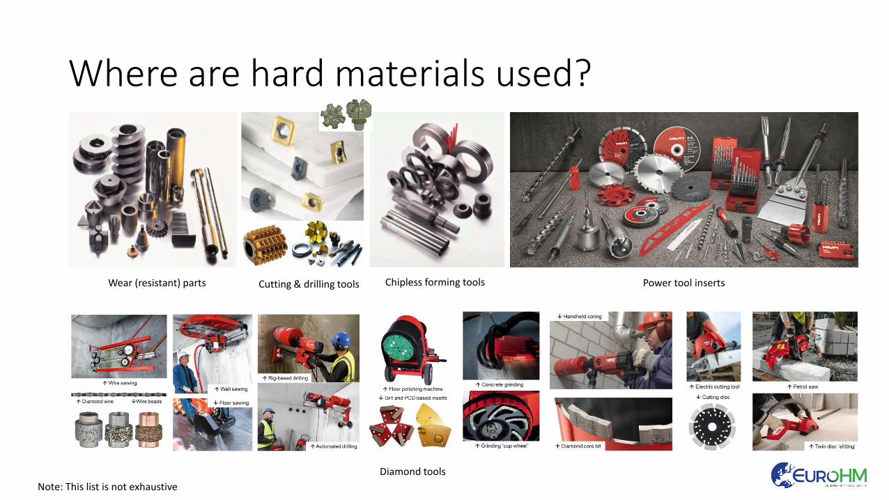
Where are hard materials used?
Wear (resistant) parts Cutting & drilling tools Chipless forming tools Power tool inserts
Diamond tools
Note: This list is not exhaustive

How are components manufactured?
• Different forming methods depending on component size and geometry
• Made from powder, shaped and sintered (example: hardmetals)
Note: Examples of hardmetals

(*) Recent developments in (*) hard materials
• PM Tool Steels (and hard phase reinforced MMCs)
• Hardmetals (cemented carbides and cermets)
• Cutting Tool Ceramics (and new hard composites)
• Coatings (CVD, PVD)
• Polycrystalline Diamond (and polycrystalline cubic boron nitride)
• Monocrystalline Diamond (and cubic boron nitride)
(*) Insert the word “some” here

PM tool steels & MMCs
• Greater purity through clean powder production
• Better microstructures and properties • fatigue & wear resistance, strength & toughness, …
• Expanded range of alloy compositions • carbon free intermetallic reinforced (maraging) steels
• very high carbon contents (carbides >25 vol%)
• mixed hard phases of carbides and borides
• complex alloy binders
• special alloys for additive manufacturing
• …
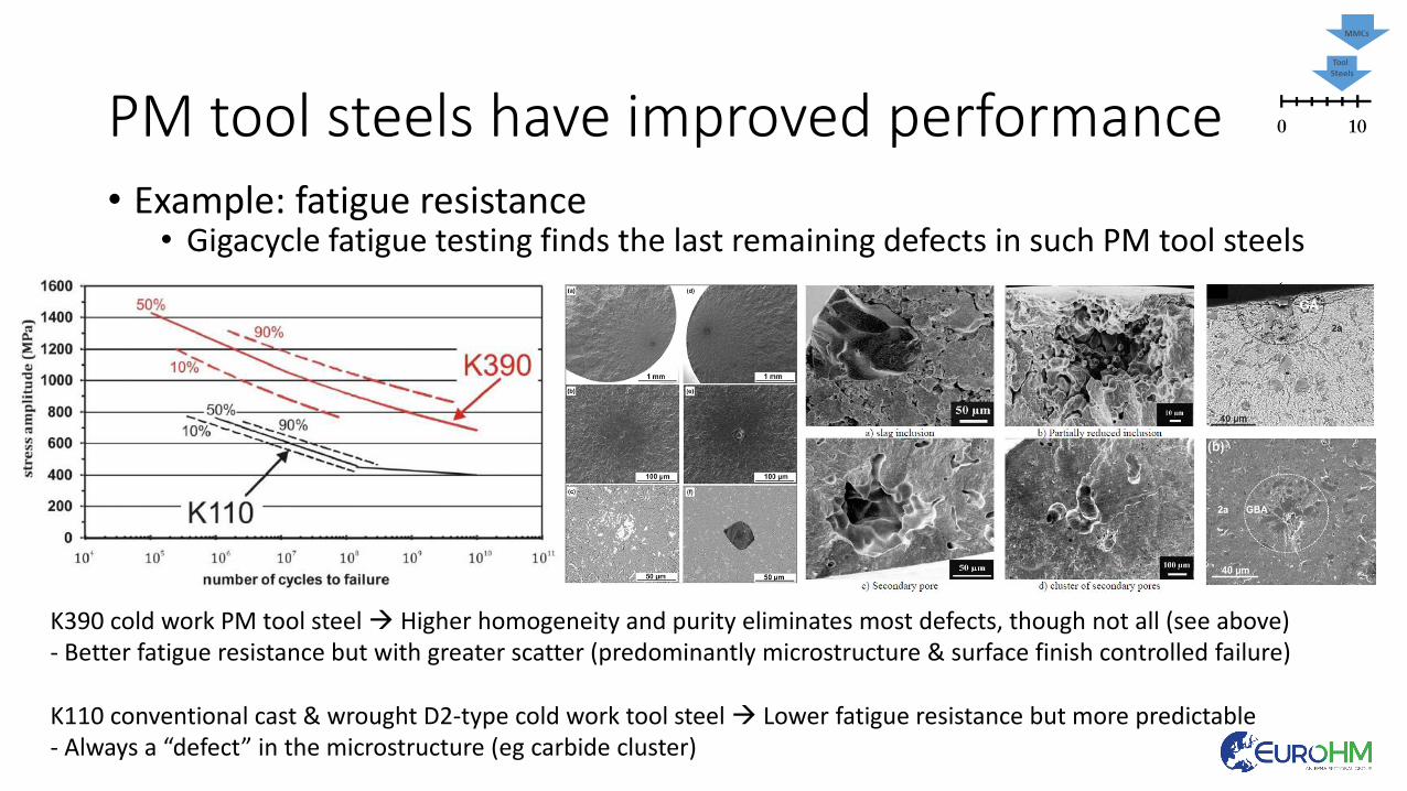
K390 cold work PM tool steel Higher homogeneity and purity eliminates most defects, though not all (see above)- Better fatigue resistance but with greater scatter (predominantly microstructure & surface finish controlled failure)
K110 conventional cast & wrought D2-type cold work tool steel Lower fatigue resistance but more predictable - Always a “defect” in the microstructure (eg carbide cluster)
PM tool steels have improved performance• Example: fatigue resistance
• Gigacycle fatigue testing finds the last remaining defects in such PM tool steels

FeCrV10 + 316L
56NiCrMoV7
1.2709Maraging Steel
Additive manufacturing of tool steels
• Today, generally lower alloyed, lower C steels, or
• Mixtures of higher-C steels and AM-suitable alloys
H11
H11 + 40% FeCrMo

Additive manufacturing of tool steels
• Some issues with laser processing of conventional tools steels, but
• AM is developing fast and learning from, e.g., the welding community
H13 tool steel on a solid support
FeCrV10
H13 with modified parameters
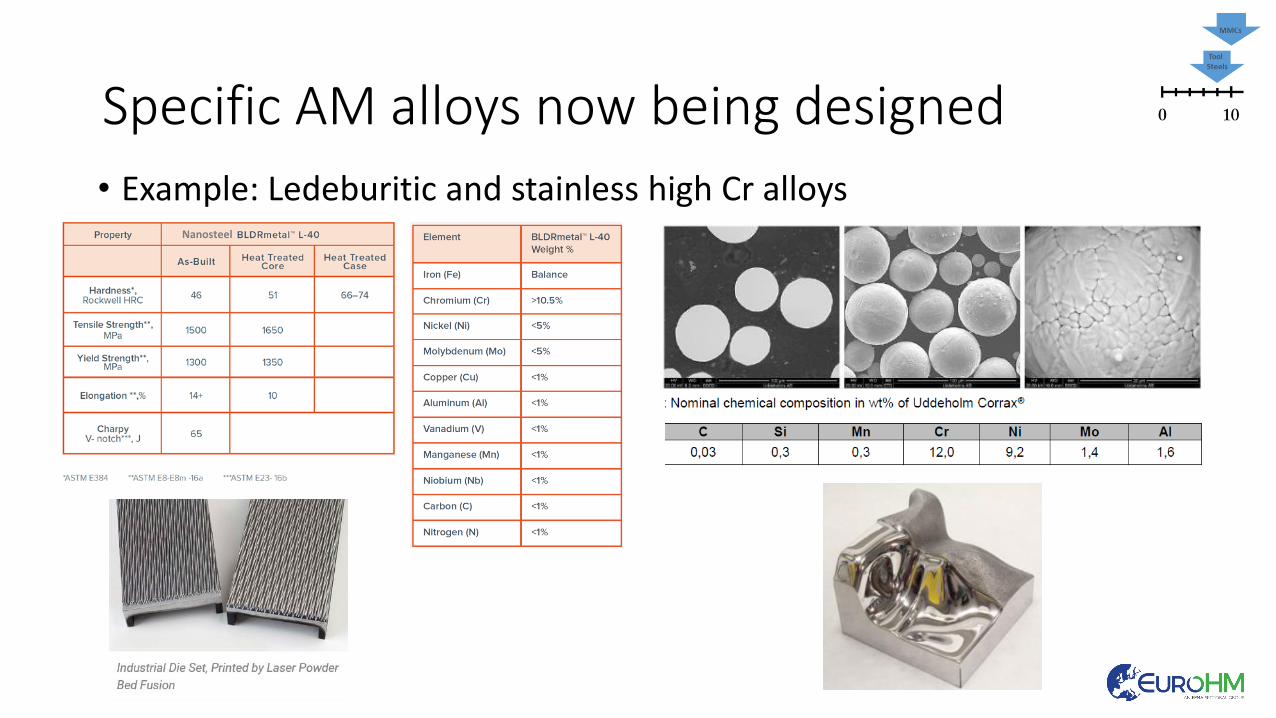
Specific AM alloys now being designed
Nanosteel
• Example: Ledeburitic and stainless high Cr alloys
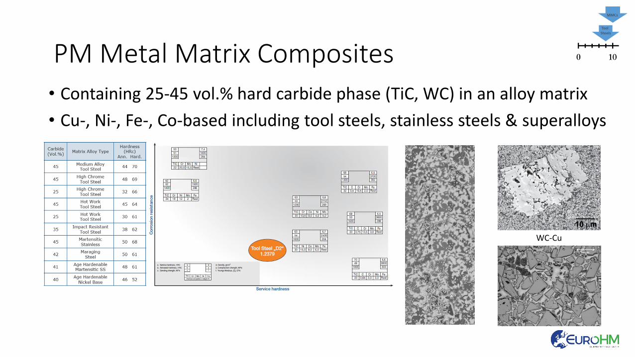
• Containing 25-45 vol.% hard carbide phase (TiC, WC) in an alloy matrix
• Cu-, Ni-, Fe-, Co-based including tool steels, stainless steels & superalloys
PM Metal Matrix Composites
WC-Cu

• E.g. containing up to 70 wt.% sintered WC spheres (50 vol.%)
• Metallic matrix of, Ni-, Co-, Inconel 625, NiSiB, …
AM Metal Matrix Composites
Electron beam processed, fully dense
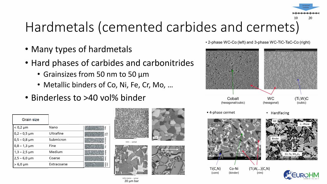
Hardmetals (cemented carbides and cermets)
• Many types of hardmetals
• Hard phases of carbides and carbonitrides• Grainsizes from 50 nm to 50 µm
• Metallic binders of Co, Ni, Fe, Cr, Mo, …
• Binderless to >40 vol% binder
20 µm bar

Hardmetals
• Binder modification by heat treatment• E.g. precipitates of Co3W or M12C with WC-Co
• Alternative binders as potential substitutes for cobalt• e.g. Fe- and Ni-based, High Entropy Alloys (HEA), intermetallics, …
Dark Blue – WCLight Blue – Cubic carbideRed – 5-component HEA Yellow – Intermetallic phase
HEA EBSD

Hardmetals
• Surface and bulk gradients• Gradients in hard phase and/or binder phase, µm to mm in depth
Note: for example only, the modelling is not the same case

Hardmetals
• Advanced characterization and modelling • Gaining a greater understanding of hardmetals from atoms to microstructures
Atom probe tomography
Density Functional Theory, cluster expansion, Monte Carlo, CALPHAD, Compound Energy Formalism, DICTRA… …and many more
Electron backscatter diffraction
Micromechanical testing (polycrystalline or single WC grain, cantilever beam or pillar)
3D reconstruction (FIB/EBSD)

AM of hardmetals
• Direct melting methods generally unsuitable for hardmetals
• AM methods for shaping followed by conventional sintering preferred
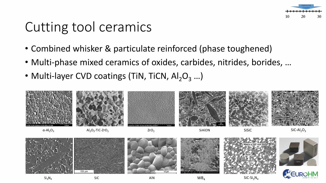
Cutting tool ceramics
• Combined whisker & particulate reinforced (phase toughened)
• Multi-phase mixed ceramics of oxides, carbides, nitrides, borides, …
• Multi-layer CVD coatings (TiN, TiCN, Al2O3 …)
SiSiC SiC-Al2O3
SiC-Si3N4

Coated hard particles and new hard composites
• CVD coatings of carbides, carbonitrides and metals onto hard particles
• Processing by sintering, HPHT, HVOF or laser metal deposition
Diamond
WC-Co
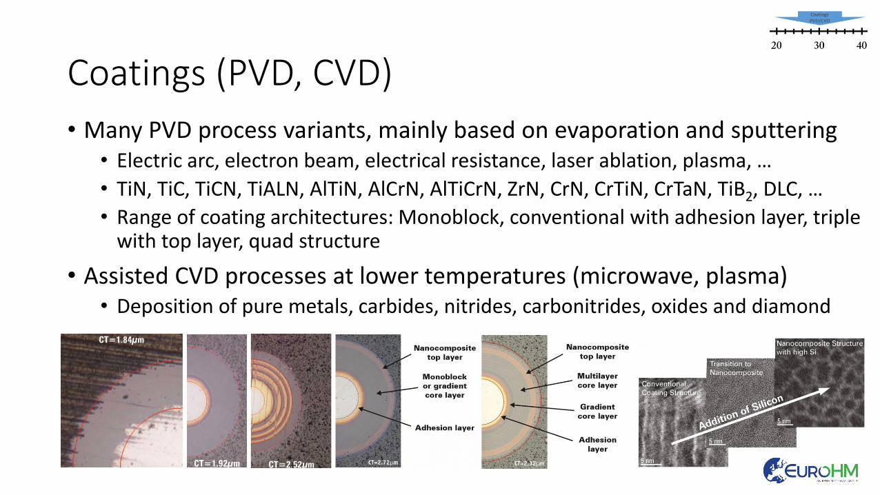
Coatings (PVD, CVD)
• Many PVD process variants, mainly based on evaporation and sputtering• Electric arc, electron beam, electrical resistance, laser ablation, plasma, …
• TiN, TiC, TiCN, TiALN, AlTiN, AlCrN, AlTiCrN, ZrN, CrN, CrTiN, CrTaN, TiB2, DLC, …
• Range of coating architectures: Monoblock, conventional with adhesion layer, triple with top layer, quad structure
• Assisted CVD processes at lower temperatures (microwave, plasma)• Deposition of pure metals, carbides, nitrides, carbonitrides, oxides and diamond

Coating stress state design possible
• Example: Comparison of two CVD coatings on WC-6Co • 3 µm multi-layer with 0.3 µm TiN adhesion layer between substrate and
carbonitride, and Ti(C,Ox) bonding layer between carbonitride and top oxide layer
• Thermally cycled (Coated-RT-800°C-RT) and stresses measured at RT and 800°C
Low stressesHigh stresses

Polycrystalline Diamond (PCD)
• Wide variety of grades available

• Wide variety of shapes and sizes available• Stress management (NPI, interlayers) and enhanced thermal stability (leaching)
Polycrystalline Diamond (PCD)
Ø80 x 8 mm discsØ25 x 25 mm cyclinders

Coated PCBN
• Wide variety of grades available, either solid or carbide backed, plus coated • Binders TiC, TiCN, AlWCoB, AlN, borides, metals, ceramics, with cBN content 45-95%
Polycrystalline Cubic Boron Nitride (PCBN)
Ø80 x 5 mm carbide backed discsØ100 x 8 mm solid PCBN
Solid PCBN

Single Crystal Diamond
• Very large single crystals (up to 10mm) by HPHT and CVD
• Crystallographically oriented for specific properties by application
For cutting tools, grinding wheel dressers, knives, wear parts and wire drawing dies

Single Crystal Diamond (and cBN) Grit
• Tailored morphologies (size and shape)
Octahedra
Cubes
12/14 mesh
30/40 mesh
cBN

Single Crystal Diamond Grit
• Tailored properties (strength, toughness, thermal resistance)
• Arranged diamonds in segments
Segment with randomly-
distributed diamonds
Segment with arranged diamonds

I hope you enjoyed this introduction to the world of hard materials…
AFM image and the depth profile of a scratch from ReB2, 230 nm deep on diamond surface
Elemental analysis confirmed a carbon surface free of rhenium
H.-Y. Chung, M.B. Weinberger, J.B. Levine, R. W. Cumberland, A. Kavner, J.-M. Yang, S.H. Tolbert, R.B. Kaner Science 316, 436 (2007).
ReB2
30-50 GPa
Diamond70-120 GPa
…even though we’ve only just scratched the surface! Thank you for your attention.