Developments, Applications and Challenges for the Industrial ......EV Group Confidential and...
31
www.EVGroup.com Martin Eibelhuber, Business Development Manager [email protected] Developments, Applications and Challenges for the Industrial Implementation of Nanoimprint Lithography
Transcript of Developments, Applications and Challenges for the Industrial ......EV Group Confidential and...

www.EVGroup.com
Martin Eibelhuber, Business Development Manager
Developments, Applications and Challenges for
the Industrial Implementation of
Nanoimprint Lithography

www.EVGroup.com EV Group Confidential and Proprietary
Outline
Introduction Imprint Lithography
Wafer Level Optics
Applications
SmartNIL™Technology
EVG® Hercules®NIL
Summary

www.EVGroup.com
Introduction
Nanoimprint Lithography

www.EVGroup.com EV Group Confidential and Proprietary
Novel device concepts need alternative
lithography solutions
Complexity of pattern design should not add
to manufacturing costs
General Explanation – UV-Nano Imprint Lithography
Why ?
How ?
What?
Nanoimprint lithography enables simple
replication of various kind of structures,
shapes and sizes
Nanoscale structures can be achieved
without sophisticated and expensive optics
EVG equipment portfolio covers all common
imprinting techniques on volume proven
systems
NILPhotonicsTM Compentence Center to link
equipment and process know-how for
innovative products
Biotechnology Photonics
Nanostructures Microlenses
EVG®620 EVG® Hercules®NIL

www.EVGroup.com EV Group Confidential and Proprietary
Hot Embossing
1) Spin coat thermoplastic film
2) Parallel alignment
3) Heat until viscous
4) Emboss at high temperature
5) Cool until solid
5) Demold stamp
Nanoimprint Lithography at a Glance
Micro Contact Printing
(µCP) Soft Lithography UV-Nanoimprint
Lithography (UV-NIL)
Transparent
Hard Stamp
Polymer
Soft Stamp
Hot Embossing
Hard Stamp
Polymer
Soft Stamp
Polymer
Soft Stamp
UV-NIL
1) Dispense liquid resin on
substrate
2) Parallel alignment
3) Imprint at low pressure
4) Expose with UV light through
stamp and crosslink
5) Demold stamp
5
www.EVGroup.com EV Group Confidential and Proprietary
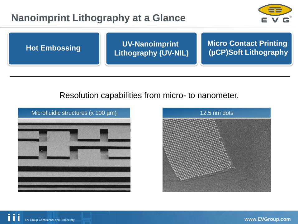
Nanoimprint Lithography at a Glance
Microfluidic structures (x 100 µm) 12.5 nm dots
Resolution capabilities from micro- to nanometer.
Micro Contact Printing
(µCP)Soft Lithography UV-Nanoimprint
Lithography (UV-NIL) Hot Embossing

www.EVGroup.com EV Group Confidential and Proprietary
Nanoimprint Lithography Results
Honeycomb Texturing for
Photovoltaics
Micro- & Nano structuring by NIL is applicable in any field of photonics.
Gratings for distributed feedback
lasers
Photonic Crystals for light
extraction of LEDs
Nano-patterend Sapphire
Substrates for LED growth
Gratings on topography 3D shaped optical elements
5 µm
2.5 µm
250 µm
15 µm

www.EVGroup.com
Wafer Level Optics
Micron and Submicron Imprinting

www.EVGroup.com EV Group Confidential and Proprietary
Wafer Level Optics
High volume manufacturing of
precise optical elements
Parallel processing of hundreds or
thousands lenses
High clarity due to turbulence free
and precise processing
Complete mold fill even for complex
structures
Enables wafer level packaging of
optical modules
Smallest form factors
9

www.EVGroup.com EV Group Confidential and Proprietary
Wafer-scale miniaturized optical systems
10
Refractive Optics Diffractive Optics
• Collimators for laser, fibers, sensors
• Multi aperture Imaging
• Microlens arrays
• Customized Microoptics
Alternative Microoptics
• Optics on CMOS
• Hybrid refractive/diffractive Source:
Fraunhofer IOF
• Pattern Projection
• Holography
• Fresnel Lenses
• Diffractive Filters or Polarizers
• Optics with complex functionality

www.EVGroup.com EV Group Confidential and Proprietary
Process Examples for Wafer Level Optics
Diffractive optical elements
Microlens arrays
Functional optical films.
Wafer-level
camera module
S&R master stamp
Single lens pin
Working stamp
Lens wafers
Source: Anteryon

www.EVGroup.com EV Group Confidential and Proprietary
WLO in (Volume) Manufacturing
EVG®770 NIL Stepper • Step & Repeat Master Stamp Fabrication
EVG IQ Aligner®
• Working stamp fabrication
• Lens molding & stacking
• Smart lens fabrication

www.EVGroup.com
Nanoimprint Lithography
Applications

www.EVGroup.com EV Group Confidential and Proprietary
NIL Unique Benefits
Large Area Nanopatterning
Resolution << Alignment
3D Pattering
Direct Patterning
Enables highest
resolution down to
20nm and less
No expensive precision
alignment optics
Wafer level processing
of nanostructures
without stitching
Scalable technology
which not limited by an
optical system
Replication process is
insensitive to shape,
size & structure
Complexity does not
add manufacturing
costs
Imprint materials can be
functionalized to
needed properties
Reduces process steps
significantly

www.EVGroup.com EV Group Confidential and Proprietary
From Imprinting to Devices

www.EVGroup.com EV Group Confidential and Proprietary
Honeycomb Texturing of Multicrystalline Silicon
(mc-Si)
Mastering using three-beam IL
(hexagonal pattern, 8 µm period)
NIL using PDMS stamps on
Rough, brittle and thin (~180 µm)
Large area (156 x 156 mm²) mc-Si
substrates
Plasma etching and subsequent wet
chemical post-treatment
Excellent optical performance
even outperforming pyramidal shapes
H. Hauser, et.al., Development of NIL processes for PV
applications; Proceedings of SPIE; 2015; in press.
0
1x10¹⁸
2x10¹⁸
3x10¹⁸
4x10¹⁸
5x10¹⁸
6x10¹⁸
Photo
n F
lux [s
-1m-2
m-1]
0,3 0,4 0,5 0,6 0,7 0,8 0,9 1,0 1,1 1,20
10
20
30
40
50
60
70
Refl
ecta
nce [
%]
Wavelength [µm]
Plane reference (mc-Si)
Isotropic texture (mc-Si)
Pyramidal texture (c-Si)
Honeycomb texture (mc-Si)
Optical efficiency opt of 87.5 %
(electrons out / photons in)
30 µm
20 µm

www.EVGroup.com EV Group Confidential and Proprietary
nPSS Fabricated by SmartNILTM
17
SEM images of 400nm pillars for nPSS
Structures
6” imprint
360 nm
200 nm
395 nm
35 nm

www.EVGroup.com EV Group Confidential and Proprietary
Solutions for Microfluidics
R&D Pilot Line HVM
micro-
channel
fabricaiton
sealing/
packaging
nanopatterns
in the channels
EVG’s Core
Competences
Lithography
Hot
Embossing
Bonding
(UV-)
Nano-
imprinting
Process Services

www.EVGroup.com EV Group Confidential and Proprietary
Saphely Project
Self amplfied photonic biosensing platform for micro RNA-
based early diagnosis of deseases
Photonic Bandgap Sensor
Gratings
manufactured
with SmartNIL! wafelength
inte
nsit
y
microRNA
analytes

www.EVGroup.com EV Group Confidential and Proprietary
Dry out
BSA-Cy5-Biotin solution
Stamp
Coated glass slide Incubation with
antibodies
BSA-Cy5 grid FITC-antibody
Schwarzenbacher et al., 2008. Nature Methods. Weghuber et al., 2010.
Methods in Enzymology. Lanzerstorfer et al., 2013. Basic Methods in Protein
Purification and Analysis.
SmartNILTM for Bio-functionalization
Bio-functionalization of µ-arrays
AFM measurement of antibodies

www.EVGroup.com
SmartNILTM Technology

www.EVGroup.com EV Group Confidential and Proprietary
SmartNILTM – Large Area Imprint
Basic elements of the technique:
Flexible UV-transparent molds
Proprietary imprint tooling SmartNILTM
Allows large area conformal imprints
www.EVGroup.com EV Group Confidential and Proprietary
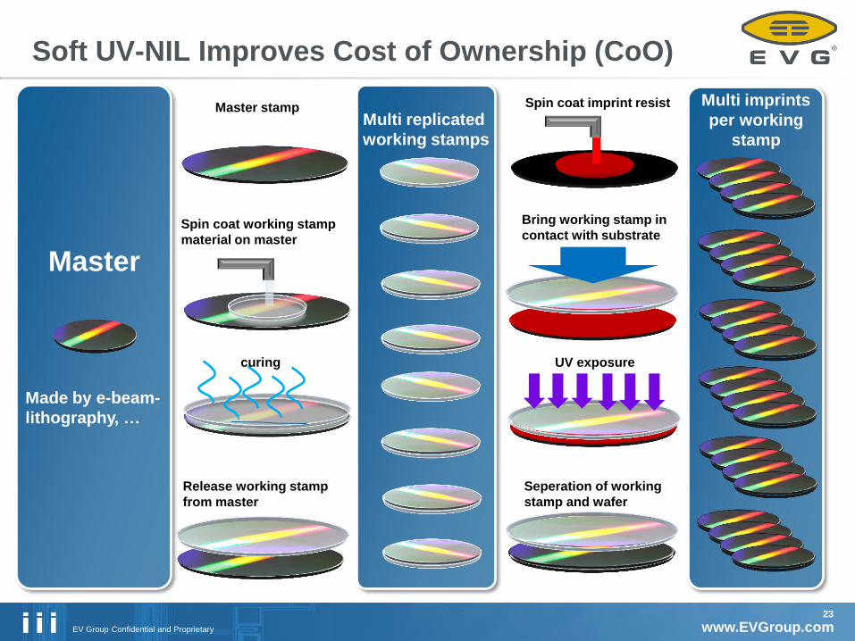
Soft UV-NIL Improves Cost of Ownership (CoO)
23
Master
Multi replicated
working stamps
Multi imprints
per working
stamp
Made by e-beam-
lithography, …
Master stamp
Spin coat working stamp
material on master
curing
Spin coat imprint resist
Bring working stamp in
contact with substrate
UV exposure
Seperation of working
stamp and wafer
Release working stamp
from master

www.EVGroup.com EV Group Confidential and Proprietary
SmartNILTM – Pattern Fidelity
24
Mean Critical Dimension
• Superior mean critical dimension variation of < 10 nm @ 3δ over all 50 imprinted substrates using the same polymer stamp.
Height
• Height variation of only < 20 nm @ 3δ over all 50 imprinted substrates using the same polymer stamp
Side Wall Angle
• Side wall angle variation of only < 2.5° @ 3δ over all 50 imprinted substrates using the same polymer stamp.

www.EVGroup.com
EVG® Hercules®NIL
Fully-integrated UV-Nanoimprint Lithography System

www.EVGroup.com EV Group Confidential and Proprietary
HERCULES®NIL
UV
Coat Module Clean Module Bake Module Imprint Module
Preprocessing
modules
The SmartNILTM
module is the heart of
the HERCULES® NIL

www.EVGroup.com EV Group Confidential and Proprietary
Volume-proven imprinting technology with superior
replication fidelity
Uniform large area imprint with high process flexibility
Fully-automated imprinting and controlled low-force
detachment for maximum working stamp reusability
SmartNIL™ tooling
Nanoimprint Module
Cleaning Module
• Excellent cleaning results for critical particle sizes
Coating Module
High uniformity spin coat module with precise
thickness control for minimum residual layer
thickness
Optimized bowl design and flow dynamics for
low resist consumption
UV

www.EVGroup.com EV Group Confidential and Proprietary
Advanced bake / chill modules
with topside heating and high
solvent exhaust
Additional Features
Internal chemical cabinet &
external chemical cabinet
for high coating uniformity due to
equal temperature of resist and
wafer
Optional mini-environment and climate control
for minimum particle contamination as well as
best process stability and yield for sensitive
processes or chemicals

www.EVGroup.com
Summary

www.EVGroup.com EV Group Confidential and Proprietary
NILPhotonicsTM Competence Center
Competence
NILPhotonicsTM
Center
Master Templates
• SU-8 Mastering
• Wide Network of stamp
suppliers
• S&R Mastering Metrology Infrastructure
• SEM, AFM,
• Interferometry
• Wide network of
metrology providers
Process Development
Definition and development
of customized processes
• UV-NIL
• Hot Embossing
• Micro-contact Printing
Sample Processing
EVG offers:
• Manufacturability
Demonstrations
• Small production run imprint
services
• Scale-up to pilot line
production
Pilot Line Production
For seamless transition from R&D
to production, EVG offers pilot line
production services as well as
process transfer to customer
designated volume manufacturing
sites
Materials Know-How
Based on its extensive process
related know-how, EVG offers
optimization of soft-stamp and
imprint resin interaction to meet:
• Applications requirements
• Layout requirements
• Productivity and low Cost of
Ownership (CoO)

www.EVGroup.com EV Group Confidential and Proprietary
Data, design and specifications may not simultaneously apply; or depend on individual equipment configuration, process conditions and materials and may vary accordingly. EVG reserves the right to
change data, design and specifications without prior notice. All trademarks, logos, website addresses or equipment names that contain the letters or words "EVG" or "EV Group" or any combination thereof,
as well as the following names and acronyms are registered trademarks and/or the property of EV Group: ComBond®, CoverSpinTM, EZB®, EZ Bond®, EZD®, EZ Debond®, EZR®, EZ Release®, GEMINI®,
HERCULES®, HyperIntegration®, IQ Aligner®, LowTempTM, NanoAlign®, NanoFillTM, NanoSprayTM, NIL-COM®, NILPhotonicsTM, OmniSpray®, SmartEdge®, SmartView®, The Triple "i" Company Invent-
Innovate-Implement®, Triple i®. Other product and company names may be registered trademarks of their respective owners.
Thank You!