Multi-resolution Data Communication in Wireless Sensor Networks
DESY PRC R&D Nr 01/04(Updated Octobre 2009)Project: CMOS sensor basedVertex Detector for the ILCStatus Report
Development of Swift, High Resolution, Pixel
Sensor Systems for a High Precision Vertex
Detector suited to the ILC Running Conditions1
Marc Wintera, on behalf of the IPHC-IRFU collaboration
in partnership with:
• LPSC-Grenoble (France) for ADC prototyping
• Oxford Univ. (UK), Bristol Univ. (UK), DESY (Germany)and Frankfurt Univ. (Germany) for ladder prototyping
31st Octobre 2009
Contact persons of the teams involved:
• IPHC/IN2P3-CNRS, Strasbourg (France): Marc Winter
• IRFU/CEA, Saclay (France): Fabienne Orsini
• LPSC/IN2P3-CNRS, Grenoble (France): Daniel Dzahini
• Oxford University, Oxford (UK): Andreı Nomerotski
• Bristol University, Bristol (UK): Joel Goldstein
• DESY, Hamburg (Germany): Ingrid-Maria Gregor
• Goethe University, Frankfurt (Germany): Joachim Stroth
a e-mail address: [email protected]
1Work supported by the European project EUDET (FP6).

Abstract
CMOS sensors are being developed to equip a vertex detector offering the perfor-mances required for the physics programme at the International Linear Collider. Theprogress realised from Spring 2007 to Autumn 2009 is exposed in this report. It pri-oritised the design of fast integrated signal processing micro-circuits. Besides this mainissue, efforts were made to organise an R&D programme addressing integration issuesrelated to a double-sided ladder concept and to power cycling.
The optimisation of the geometry of a high precision vertex detector best adapted tothe running conditions near the ILC interaction point was refined, supported by a newestimate of the occupancy induced by beam related background.
Contents:
1) Executive summary
2) Updated ILC vertex detector specifications
3) Fast integrated read-out architecture
4) Next steps of the sensor development
5) R&D en system integration issues
6) Conclusions
Appendix: short description of MIMOSA sensors mentionned in the report
More information on all activities described in this document may be found on theweb site of IPHC: http://www.iphc.cnrs.fr/Cmos.html
1 Executive summary
• Introduction
Swift, high resolution, thin CMOS pixel sensors are being developed for an ILC MicroVertex Detector (VXD), allowing for high precision displaced vertex reconstruction in ahigh hit density environment. Designed at IPHC and IRFU, the sensors are manufacturedby the CMOS industry and can - consecutively - be thinned down to ≤ 50 µm. The sensorR&D incorporates radiation tolerance and power dissipation constraints. It is complementedby an R&D programme addressing the system integration, aiming at ultra-light ladderscompatible with power cycling in a high magnetic field. The developments are accompaniedby a progressive refinement of the detector geometry, providing the necessary guidance tothe sensor design.
• Achievement of a full scale swift and accurate sensor
Since the last PRC review (May 2007), most of the R&D activities were devoted tothe achievement of a fast, full scale, sensor with all performances being in the ball park ofthose required for the VXD. The main challenge of this prototyping line concerned the read-out speed, which needed to come close to 100 µs. An integrated micro-circuit architecturewas developed, where the signals delivered by the sensors are discriminated before beingfiltered by an integrated zero-suppression logic. The fast read-out is achieved by groupingthe pixels composing the sensitive area in columns read out in parallel. The developmentof this architecture relied on two parallel tasks. One of them addressed the upstream partof the signal conditionning chain, ranging from the pixel array to the discriminators endingthe columns. The other concerned the downstream part, combining a zero-suppression logicwith output memories and the data transmission circuitry.
Small prototypes were fabricated and tested in previous years to develop the upstreampart of the sensor architecture (see sub-section 3.1). MIMOSA-22 is the final prototype ofthis R&D line supported by the European project EUDET. Two complementary versionswere designed and fabricated. They both feature 136 columns read out in parallel, eachcontaining 576, 18.4 µm pitch, pixels. 128 columns are ended with a discriminator, while 8columns have analogue outputs for test purposes. The chips incorporate a JTAG controller.The frame read-out time is 92.5 µs. Various pixel designs were integrated in the chips,allowing to explore different sensing diode sizes, amplification schemes, ionising radiationtolerant designs, etc.
Both sensors were extensively tested in 2008. A modest noise value was found for mostpixel designs, ranging from about 10 to 14 e−ENC, with a mild operating temperaturedependence. The 128 discriminators exhibited a modest threshold dispersion (± 4 % standarddeviation) and contributed marginally to the total noise. No significant non-uniformity wasfound over the sensitive area of any of the 6 sensors tested. When exposed to a 120 GeV π−
beam at the CERN-SPS, a signal-to-noise ratio (SNR) in the range 17–21 (most probablevalue) was observed, depending on the pixel design, translating into a detection efficiency of99.8 ± 0.1 % for a fake hit rate well below 10−4. The single point resolution was measuredto be around 3.7-3.8 µm. The impact of ionising radiation on these performances wasevaluated for integrated doses of 150 and 300 kRad (typical doses for a few years of ILCoperation at 500 GeV). A decrease of the SNR was observed at room temperature. The
1
consequence on the detection efiiciency and fake hit rate was negligible for 150 kRad. For300 kRad, the effect was more sizeable, and triggered the fabrication of MIMOSA-22bis. Thedesign corrections implemented in this chip alleviated the noise increase observed previously,allowing to validate the pixel design up to this range of integrated dose. Globally, the testsof MIMOSA-22 and -22bis validated the column parallel architecture and allowed to selecta pixel design suited to the ILC requirements.
The zero-suppression micro-circuitry and the output memories composing the down-stream part of the sensor architecture were prototyped with a chip called SUZE-01 (seesub-section 3.2). Its design is adapted to the output of 128 columns and to a hit density perraw of up to 3. Fabricated in 2007 within the EUDET project, it was tested extensively atIPHC until Spring 2008, with millions of patterns, at its nominal clock frequency (100 MHz)and above. No failures were spotted for frequencies ≤ 115 MHz. This guaranteed that thearchitecture is suited to the complete sensor specifications.
Next, a complete, full scale, sensor (called MIMOSA-26) was designed in 2008 withinthe EUDET project and sent for fabrication. It combines the architecture of MIMOSA-22 and SUZE-01 in a comprehensive charge sensing and signal read-out chain, providingdiscriminated signals in a binary mode including the pixel address (see sub-section 3.3). Itfeatures 1152 columns of 576 pixels, read out in ∼ 110 µs. It was extensively tested withradioactive sources and at the CERN-SPS. The pixel performances were found identical tothose of MIMOSA-22/-22bis and the SUZE-01 test results were faithfully reproduced. Theonly difference concerned the dispersion of the discriminator thresholds, which was observedto be larger than in MIMOSA-22. This resulted in a somewhat maginal increase of thetotal noise. Based on these very satisfactory results, the sensors (thinned to 120 µm) weremounted on the 3 planes composing each of the two arms of the EUDET beam telescope, andoperated smoothly. 6 sensors were also combined in a separate telescope for their performanceassessment. The results obtained confirmed that the sensor architecture is well suited to anILC vertex detector and is therefore worth extending to match its specifications.
• First use of CMOS sensors in a collider experiment
MIMOSA-22 and -26 were used to derive variants adapted to the vertex detector of theSTAR experiment at RHIC, within the framework of its upgrade (see sub-section 4.3.2). Theextension of MIMOSA-22, called MIMOSA-23, was fabricated in 2008 and is presently beingintegrated in the vertex detector. It is composed of 640 columns of 640 pixels with a 30 µmpitch. It acts as a forerunner of the final detector version, and will therefore only cover 30 %of the detector acceptance. It is expected to start data taking for physics in 2011. It shouldprovide the first final states composed of displaced vertices, coming from charmed mesondecays, identified with CMOS sensors.
The MIMOSA-26 architecture is now being extended to a 2x2 cm2 sensor adapted tothe final version of this vertex detector. The chip will be sent for fabrication early in 2010,and will start to be operated for physics studies in 2012. The use of MIMOSA sensors inSTAR is an important step towards the use of the sensors in an ILC vertex detector. Thisis firstly because the STAR vertex detector construction, which consists in assembling 400sensors on 40 ladders, each featuring ∼ 0.3 % X0, allows investigating numerous technicaland engineering aspects, which would occur while constructing an ILC vertex detector. Theother reason is that it will allow operating a complete detector made of CMOS sensors (atroom temperature), and exploiting its data for charm tagging.
2
• Update of the ILC vertex detector requirements
To adapt the MIMOSA-26 architecture to an ILC vertex detector, the assessment ofthe detector requirements, already started in previous years, was refined (see section 2).Detailed GEANT simulations of the beamstrahlung background were performed for thispurpose within the framework of the ILD Letter of Intent (LoI). The occupancy estimatedfor the LDC design was updated. In comparison with previous, less accurate, estimates, thepresent study showed that the occupancy in the detector innermost layer may easily reachseveral per-cent with the sensor integration time usualy assumed in this design (i.e. 50 µs).The study also shows that sensors featuring a thin sensitive volume (e.g. 15 µm thick) leadto a substantialy reduced occupancy. It confirmed the added value of the shorter integrationtimes ambitionned for the MIMOSA sensors, which range from 25 µs in the innermost layer to100 µs in the outer layers. It also confirmed that the background rejection gets significantlyimproved with an integration time of 50 µs in the second layer (instead of 200 µs assumedfor the LDC design).
• Towards sensors adapted to an ILC vertex detector
First studies were performed, to derive from MIMOSA-26 a sensor satisfying the ambi-tioned 25 and 50 µs read-out times (see sub-sections 4.1 and 4.2). The speed improvementwill result from reducing the number of pixels per column, and from implementing a double-sided read-out. These changes will be complemented by a an improvement of the sensorclocking. The pixel pitch will be reduced to . 15 µm in order to achieve a single pointresolution of less than 3 µm with binary signals. Finally, the sensor will be manufacturedin a CMOS process with a feature size well below the 0.35 µm presently used (essentiallyfor budget concerns). The double-sided read-out design will be prototyped in 2010, as wellas the exploration of a newly available 0.18 µm technology. These efforts may be comple-mented with the production of sensors featuring elongated pixels, which would translate intoless pixels per column and therefore result in a shorter integration time.
Due to the fast fading of the beam background with increasing distance to the beamlines, the outer layers can be read out in 100 µs. Another difference with the innermost layeris the pixel pitch, which may be doubled. The outer layer sensor derived from MIMOSA-26will therefore feature an integration time of about 100 µs and a pixel pitch in the range 30–35 µm (see subsection 4.3). This pitch size garantees the necessary read-out time for 2 cmlong columns (by limiting the number of pixels per column to 550–650). To keep the singlepoint resolution to ∼ 3 µm, each column will be terminated with a 4- or 5-bit ADC. Severalalternative ADC versions were already designed and fabricated (see sub-section 3.4). Theprototyping concentrated on the ADC dimensions and aspect ratio, on the signal processingspeed and on power dissipation. Though still limited to devices with a small number ofchannels, satisfactory performances were obtained. They need now to be confirmed withchips featuring a larger number of channels, and including discrimination functionalities.Next, the first pixel array equipped with ADCs should be designed. It is planned for 2010/11.
• System integration activities
Within the ILD LoI studies, an alternative approach to the detector 5-layer geometryassumed up to now was considered. It is based on 3 double-layers, each ladder hostingsensors on each of its two faces. This design is expected to offer several features improvingthe impact parameter resolution. It is however suspected to be technicaly more challenging
3
than the 5 single-layer geometry. A preliminary study of the pros and cons of the double-sided ladder concept was initiated. It shows in particular that the background rejection, thedetector alignment and the matching of tracks in the forward region would definitely benefitfrom this design. Its feasibility is being investigated since the beginning of 2009 within adedicated project called PLUME2 (see sub-section 5.1). It aims at realising, by 2012/13, adouble-sided ladder prototype with a total material budget not exceeding 0.3–0.4 % X0. Thedeadline is to be regarded as coinciding with the next major deadline of the ILC project, i.e.the Technical Design Report (TDR) relying on a Detailed Baseline Design (DBD).
The ladder is foreseen to host 6 butted MIMOSA-26 sensors on each of its faces. Thesensors will be mounted on a thin flex cable and assembled on a SiC foam mechanical support.The ladder will thus feature an active area of about 1×12.5 cm2. These dimensions are veryclose to those foreseen for the ILD vertex detector innermost layer.
The project includes power cycling tests inside a high magnetic field. It is based on 3or 4 consecutive prototypes. The first one (labelled ladder-0) is already well advanced. It ismainly supposed to explore basic difficulties and obstacles inherent to the project. It consiststherefore of only 2 pairs of butted MIMOSA-20 sensors (each being 1×2 cm2 large), thinnedto 50 µm. The ladder total material budget amounts to ∼ 0.6 % X0. Two such ladders werefabricated in 2009. One of them will be tested at the CERN-SPS in November 2009, withvarious incidence angles of the beam particles. The next prototype, to be fabricated in 2010,will be made of the final number of MIMOSA-26 sensors. It will still depart from the finalladder by its less agressive material budget, which is expected to amount to ∼ 0.6 % X0.At present, the flex cable needed for this prototype has been fabricated in Oxford and thenecessary MIMOSA-26 sensors are soon going to be thinned to 50 µm.
Besides the PLUME project, attempts are made to exploit an emerging packaging tech-nique, which consists in embedding thinned, edgeless, sensors butted on a very thin flex cableand consecutively wrapped with a thin polymerised film (see sub-section 5.2). The system,which was named SERWIET3 will be relatively flexible and adaptable to various mechanicalsupport shapes. It may therefore be curved according to a cylindrical shape, which wouldopen the possibility to mount the sensors directly on the beam pipe. This ambitious projecthas been started recently within the (approved) E.U.-FP7 project called Hadron Physics 2.
• Vertically integrated CMOS sensors
Vertical integration technologies have gone through striking progresses in the last yearsand have recently become accessible to the academic world. An R&D programme addressinga new generation of CMOS sensors exploiting the added value of these technologies wasstarted in 2009, within a consortium coordinated by FNAL (see sub-section 4.4.3). Thesetechnologies are particularly attractive for CMOS pixel sensors as they allow to stack inthe shadow of each pixel complexe micro-circuitry distributed over several interconnectedtiers. The limitations in the transistor type encountered with ordinary CMOS sensors aretherefore alleviated, as well as the contraints imposed by the narrow pixel dimensions andby the restricted amount of metal layers. Moreover, different fabrication processes can becombined in a single device. This allows realising a sensor where each tier is fabricated in aspecific process best suited to its functionalities. For instance, a process featuring an epitaxiallayer of the right thickness but offering a too large feature size and too few metal layers can
2standing for Pixelated Ladder with Ultra-light Material Embedding3standing for SEnsor Row Wrapped In an Extra-Thin film
4
be interconnected with another, VDSM, process relying on twice more metal layers ensuringthe signal processing. The latter can be distributed other several (typicaly 10 µm thin) tiers.Consequently, the read-out is expected to speed-up by at least one ordre of magnitude w.r.t.ordinary 2D sensors.
The potential of this new sensor generation was investigated with an engineering run ina 130 nm technology. The latter being based on a low resistivity substrate, it is expected toallow detecting charged particles. The chips were submitted to foundry by July 2009. Theprocess was limited to 2-tier chips. One of the chips fabricated is foreseen to be connectedto a third chip, manufactured in a different (600 nm) CMOS process. The main features ofthe chips submitted, called CAIRN4 are summarised hereafter:
• CAIRN-1 is a 2-tier sensor featuring a 12 µm pitch pixel array. It incorporates in-pixel signal discrimination and time stamping. The read-out is delayed beyond a frameintegration duration of ∼ 1 ms, adapted to the ILC beam time structure. This isexpected alleviating substantialy the power dissipated. Time stamping within eachbunch train is achieved with a 5-bit latch, complemented with an overflow bit indicatingif the pixel was hit twice within the same train. The pixel pitch was chosen smallenough for this to occur at the per-cent level only. The latch implemented in thechip is a forerunner of a future design expected to provide 6 or 7 bit time resolution,corresponding to time slots of ∼ 15 or 7 µs respectively.
• CAIRN-2 is another 2-tier sensor optimised for low power dissipation. The latter isobtained by subdividing the sensitive area into small, identical, sub-arrays operated inparallel. Each sub-array is running in a column parallel, rolling shutter, mode. Anamplifier and a discriminator are incorporated in each pixel, and the sensor read-outmay be either continuous or delayed as in CAIRN-1. The small dimensions of the sub-arrays and the fast signal circuitry are expected to allow for a frame read-out time of afew µs only.
• CAIRN-3 is a 2-tier read-out chip of a sensing device to be manufactured in a differentCMOS process, to which it will be connected using vertical integration techniques. Thisconnection will be used for signal shaping. The expected frame read-out time amountsto a few µs only. The sensors foreseen to be connected to this chip have been sent forfabrication, and are expected to come back from foundry early in 2010.
These prototypes will be tested by Spring or Summer 2010. They are expected to seta new performance standard, in particular in terms of read-out speed, resulting typicallyin a reduction of the occupancy in the VXD innermost layer by one ordre of magnitude.In comparison with 2D sensors, this technology is however still poorly known and needstherefore several years of studies and assessment. Concerns address in particular the powerextraction, radiation tolerance, pick-up noise and the material budget. At present, 3D sensorsmay therefore be considered as second generation devices, needed for instance when the ILCcollision energy will be raised to ∼ 1 TeV.
4standing for CMOS Active pixel sensors with vertically Integrated Read-out and Networking functional-ities
5
2 Updated vertex detector design specifications
The ILC vertex detector requirements are mainly driven by two competing sources of con-straints: the physics goals, which dictate the required granularity and permitted materialbudget, and the running conditions, which impose the read-out speed and the radiationtolerance. Moreover, high granularity and fast read-out tend to be in contradiction and togovern the power dissipation, which has to accommodate material budget and ladder stabilityconstraints.
This section provides an insight of how the relative weights of these conflicting detectorconcept requirements were balanced and translated into sensor (and ladder) specifications. Itshows in particular how some choices were made, which are optimal for the sensor technologydescribed in this document [1], [2]. The specifications therefore integrate the most recentprogress achieved in the sensor R&D, which is exposed in this report.
The R&D strategy leading (progressively) to performances satisfying these specificationsrelies on shorter term, less ambitious, intermediate objectives. The latter serve as validationsteps of the path towards the ILC vertex detector requirements.
2.1 Baseline vertex detector geometries
The detector design guiding the development of MIMOSA sensors is described in the ILDLettre of Intent (LoI) [3]. Its geometry is fully cylindrical and appears in two alternatives.One of them consists in 5 layers of single-sided ladders, while the other relies on 3 double-sidedladders (i.e. each ladder being equipped with sensors on both faces). For both geometries,the sensitive area of the innermost layer is 12.5 cm long while it is 25.0 cm long in the otherlayers (a priori based on 2, 12.5 cm long, butted ladders). The two sides of the double-sidedladders are about 2 mm apart. Figure 1 displays an artist view of each geometry.
2.2 Requirements
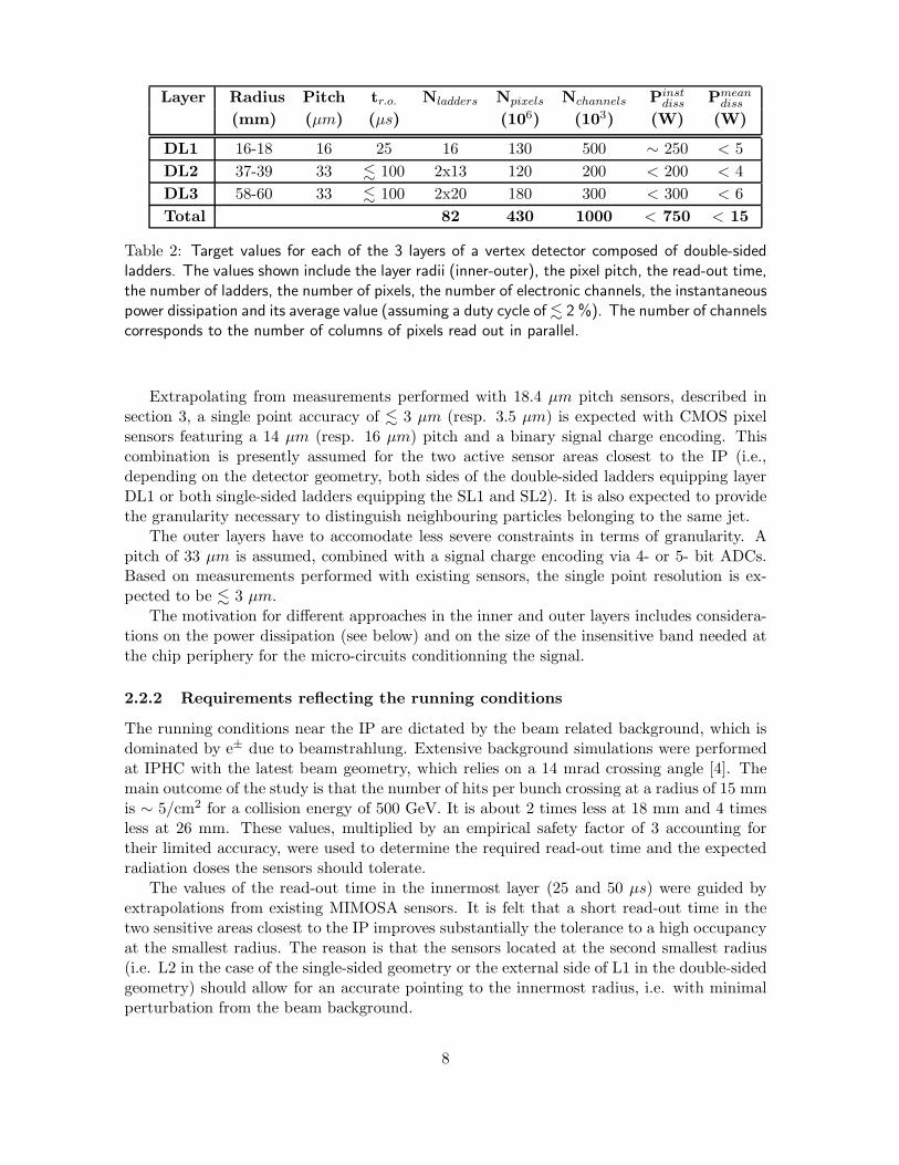
Some of the main parametres entering the set of requirements to be fullfiled by the sensorsare summarised in Table 1 for the single-sided geometry and in Table 2 for the double-sidedone. The way some of these numbers were derived is discussed hereafter.
2.2.1 Requirements on the accuracy
The impact parametre resolution expected from the vertex detector is expressed by the usualgaussian expression:
σip = a ⊕ b/p · sin3/2θ (1)
where a and b are requested to be below 5 µm and 10 µm·GeV/c, respectively. Severalstudies show that these specifications are met with a single point accuracy of . 3 µm for afirst measured point of tracks at ∼ 15 mm from the IP. In case of the double-sided ladderdesign, a single-point resolution of ∼ 3.5 µm is sufficient because the innermost layer providestwo, almost independent, measurements of the tracks’ impact position closest to the IP.
The material budget between the Interaction Point (IP) and the first measured pointshould not exceed a few permill of radiation length, which translates into an upper boundon the ladder material budget in the ordre of 0.2 % X0.
6
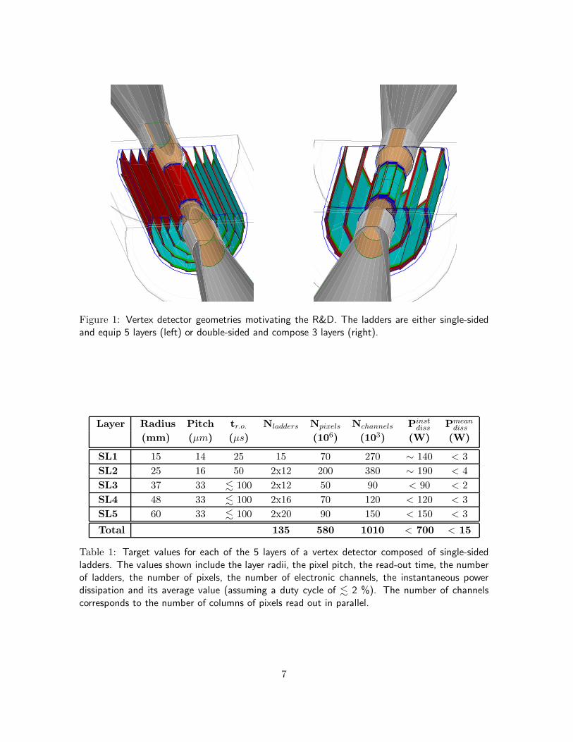
Figure 1: Vertex detector geometries motivating the R&D. The ladders are either single-sidedand equip 5 layers (left) or double-sided and compose 3 layers (right).
Layer Radius Pitch tr.o. Nladders Npixels Nchannels Pinstdiss Pmean
diss
(mm) (µm) (µs) (106) (103) (W) (W)
SL1 15 14 25 15 70 270 ∼ 140 < 3
SL2 25 16 50 2x12 200 380 ∼ 190 < 4
SL3 37 33 . 100 2x12 50 90 < 90 < 2
SL4 48 33 . 100 2x16 70 120 < 120 < 3
SL5 60 33 . 100 2x20 90 150 < 150 < 3
Total 135 580 1010 < 700 < 15
Table 1: Target values for each of the 5 layers of a vertex detector composed of single-sidedladders. The values shown include the layer radii, the pixel pitch, the read-out time, the numberof ladders, the number of pixels, the number of electronic channels, the instantaneous powerdissipation and its average value (assuming a duty cycle of . 2 %). The number of channelscorresponds to the number of columns of pixels read out in parallel.
7
Layer Radius Pitch tr.o. Nladders Npixels Nchannels Pinstdiss Pmean
diss
(mm) (µm) (µs) (106) (103) (W) (W)
DL1 16-18 16 25 16 130 500 ∼ 250 < 5
DL2 37-39 33 . 100 2x13 120 200 < 200 < 4
DL3 58-60 33 . 100 2x20 180 300 < 300 < 6
Total 82 430 1000 < 750 < 15
Table 2: Target values for each of the 3 layers of a vertex detector composed of double-sidedladders. The values shown include the layer radii (inner-outer), the pixel pitch, the read-out time,the number of ladders, the number of pixels, the number of electronic channels, the instantaneouspower dissipation and its average value (assuming a duty cycle of . 2 %). The number of channelscorresponds to the number of columns of pixels read out in parallel.
Extrapolating from measurements performed with 18.4 µm pitch sensors, described insection 3, a single point accuracy of . 3 µm (resp. 3.5 µm) is expected with CMOS pixelsensors featuring a 14 µm (resp. 16 µm) pitch and a binary signal charge encoding. Thiscombination is presently assumed for the two active sensor areas closest to the IP (i.e.,depending on the detector geometry, both sides of the double-sided ladders equipping layerDL1 or both single-sided ladders equipping the SL1 and SL2). It is also expected to providethe granularity necessary to distinguish neighbouring particles belonging to the same jet.
The outer layers have to accomodate less severe constraints in terms of granularity. Apitch of 33 µm is assumed, combined with a signal charge encoding via 4- or 5- bit ADCs.Based on measurements performed with existing sensors, the single point resolution is ex-pected to be . 3 µm.
The motivation for different approaches in the inner and outer layers includes considera-tions on the power dissipation (see below) and on the size of the insensitive band needed atthe chip periphery for the micro-circuits conditionning the signal.
2.2.2 Requirements reflecting the running conditions
The running conditions near the IP are dictated by the beam related background, which isdominated by e± due to beamstrahlung. Extensive background simulations were performedat IPHC with the latest beam geometry, which relies on a 14 mrad crossing angle [4]. Themain outcome of the study is that the number of hits per bunch crossing at a radius of 15 mmis ∼ 5/cm2 for a collision energy of 500 GeV. It is about 2 times less at 18 mm and 4 timesless at 26 mm. These values, multiplied by an empirical safety factor of 3 accounting fortheir limited accuracy, were used to determine the required read-out time and the expectedradiation doses the sensors should tolerate.
The values of the read-out time in the innermost layer (25 and 50 µs) were guided byextrapolations from existing MIMOSA sensors. It is felt that a short read-out time in thetwo sensitive areas closest to the IP improves substantially the tolerance to a high occupancyat the smallest radius. The reason is that the sensors located at the second smallest radius(i.e. L2 in the case of the single-sided geometry or the external side of L1 in the double-sidedgeometry) should allow for an accurate pointing to the innermost radius, i.e. with minimalperturbation from the beam background.
8
The read-out times in the inner layers may be considered as slightly optimistic expec-tations for two-dimensionnal sensors. Sensors exploiting vertical integration technologieshowever (see section 4.5.3) are likely to allow for read-out times of a few µs only. Such animprovement would be particularly beneficial as the values of Table 3 may be critical if thebackground rate happens to be an ordre of magnitude above the present Monte-Carlo expec-tations. Moreover, they would presumably be required when running at a collision energy of1 TeV, where the beam realted background is likely to be substantially higher than at 500GeV.
The rate of beamstrahlung e± considered for the computation of the radiation dosesaffecting the innermost layer refers to the simulated value (5 hits/cm2/BX ) multiplied bythe safety factor (3 ) and integrated over one year (107 s ). An annual rate of 2×10¹² e±/cm2
was obtained.The corresponding integrated ionising dose was calculated accounting for the number of
pixels hit per cluster and for the angle of incidence of the particles (which translates intoelongated, enlarged, clusters ). The annual dose was found to be 150 kRad. At least 2 yearsof operation were assumed before replacing the sensors, meaning that the requirement onthe sensor tolerance is 300 kRad.
The non-ionising radiation damage induced by beamstrahlung e± was computed assum-ing a NIEL factor of 1/20, as a consequence of their low momentum (10 MeV electronshave a NIEL factor of ∼ 1/30). The fluence derived from the annual rate is therefore1×1011 neq/cm
2. Assuming at least 2 years of operation before replacing the sensors, thelatter are required to tolerate a fluence of 2×10¹¹ neq/cm
2. This value is at least one ordreof magnitude beyond the one induced by the expected neutron gas circulating inside theapparatus (109−10 neq/cm
2).
2.2.3 Power dissipation
The instantaneous power dissipation was computed on the basis of the dissipation anticipatedper pixel column. Based on existing sensors (see section 3), the consumption per columnwas estimated to 500 µW in absence of an ADC ending the column, and to < 1 mW in caseeach column ends with a 4-5 bits ADC including a discriminator.
The average power consumption was computed with the hypothesis of power cycling. Itwas assumed, conservatively, that for each ∼ 1 ms long bunch train, the sensors would in factbe active during . 4 ms, corresponding to a duty cycle of . 2 %. Even with this conservativeapproach, the average power consumption for the complete detector remains below 15 W, avalue which is expected to be compatible with air flow cooling at a low circulation speed,thus minimising potential ladder vibrations diluting the resolution on the impact parametre.
3 Fast integrated read-out architecture
The read-out times required for the ILC vertex detector (i.e. 25 to 100 µs) cannot be obtainedwith full scale sensors made of several 105 pixels delivering unfiltered output signals. Suchdevices are bound to frame read-out frequencies . 1 kframe/s. Aiming for higher read-out fequencies fosters grouping the pixels in columns read out in parallel and filtering the(digitised) signals on the chip.
This architecture was cleared out with the prototypes MIMOSA-6 [5], -8 [6] and -16 [7],fabricated several years ago. They feature pre-amplification and Correlated Double Sampling
9
(CDS) micro-circuits integrated in each pixel. The latter are grouped in columns read out inparallel and ended with a discriminator. The sensor performances were presented in previousPRC reviews [8], [9]. The main outcome of this series of prototypes was a viable pixel design,exhibiting low noise and a satisfactory gain, as well as a low noise and fast discriminatordesign.
A real scale prototype, called MIMOSA-22, derived from MIMOSA-16 [7], was fabri-cated during Winter 2007/2008. A zero-suppression micro-circuit (called SUZE-01), wasdeveloped in parallel, preparing for a complete sensor, which would incorporate signal fil-tering downstream of the discriminator outputs. The complete sensor, called MIMOSA-26,was fabricated in 2009.
The 3 chips (MIMOSA-22, SUZE-01 and MIMOSA-26) were realised within the frame-work of the EU-FP6 project EUDET [10]. Their characteristics and test reults are sum-marised in this section.
3.1 Characteristics and performances of MIMOSA-22
3.1.1 Sensor description
MIMOSA-22 [11] was fabricated in the same CMOS technology (AMSC35B4O1 CMOS-Opto 0.35 µm [12]) as MIMOSA-16. The latter being only made of 24 columns of only128 pixels (i.e. 3072 pixels in total), it was necessary to reproduce its performances over asubstantially larger surface and for a number of columns closer to the final one (e.g. in orderto investigate potential dispersions between discriminators). Moreover, the pixel architectureimplemented in MIMOSA-16 was not optimised in terms of signal-to-noise ratio (SNR) andradiation tolerance, and the pixel pitch (25 µm) was too large for the single point resolutionambitionned (see section 2.2.1). Finally, the sensor was not yet equipped with the necessarycontrolling and testing features provided by JTAG.
2 versions of the sensor were designed and manufactured. The first version (MIMOSA-22) was mainly used for defining the overall pixel architecture, while the second version(MIMOSA-22bis) was used to make the design more robust, to fine tune its parametresand to improve its tolerance to ionising radiation. The goal was to validate at least one ofthe designs implemented in the chip, and then to merge it with the SUZE-01 design in thearchitecture of the complete sensor, MIMOSA-26.
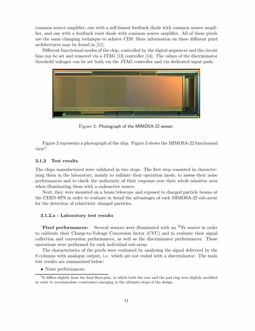
Both MIMOSA-22 prototypes have full dimensions of 12.0 x 3.7 mm2, including a chargesensitive area of 10.6 x 2.5 mm2.
The charge sensitive array contains 136 columns and 576 rows of pixels. The latter have apitch of 18.4 µm. 128 columns are ended with a discriminator featuring a common adjustablethreshold for analogue-to-digital conversion. The remaining 8 columns have direct analogueoutputs for functionnality tests and pixel characterization purposes. The outputs of the 128column level discriminators are multiplexed by a serializer block onto 16 binary output pads.The pixel array is designed to be read out on a column parallel basis and row by row (i.e.rolling shutter mode) with a frequency of 6.25 MHz. The corresponding integration time is92.5 µs.
In order to realise the MIMOSA-26 sensor with optimised performances, different sens-ing diode dimensions, with and without radiation hard structures, have been implemented inMIMOSA-22 to find the best signal detection conditions, essentially governed by the SNR.Moreover, three types of pixel architectures were implemented: one with a reset diode with
10
common source amplifier, one with a self-biased feedback diode with common source ampli-fier, and one with a feedback reset diode with common source amplifier. All of these pixelsuse the same clamping technique to achieve CDS. More information on these different pixelarchitectures may be found in [11].
Different functionnal modes of the chip, controlled by the digital sequencer and the circuitbias can be set and removed via a JTAG [13] controller [14]. The values of the discriminatorthreshold voltages can be set both via the JTAG controller and via dedicated input pads.
Figure 2: Photograph of the MIMOSA-22 sensor.
Figure 2 represents a photograph of the chip. Figure 3 shows the MIMOSA-22 functionnalview5.
3.1.2 Test results
The chips manufactured were validated in two steps. The first step consisted in character-ising them in the laboratory, mainly to validate their operation mode, to assess their noiseperformances and to check the uniformity of their response over their whole sensitive areawhen illuminating them with a radioactive source.
Next, they were mounted on a beam telescope and exposed to charged particle beams atthe CERN-SPS in ordre to evaluate in detail the advantages of each MIMOSA-22 sub-arrayfor the detection of relativistic charged particles.
3.1.2.a - Laboratory test results
Pixel performances: Several sensors were illuminated with an 55Fe source in ordreto calibrate their Charge-to-Voltage Conversion factor (CVC) and to evaluate their signalcollection and conversion performances, as well as the discriminator performances. Theseoperations were performed for each individual sub-array.
The characteristics of the pixels were evaluated by analysing the signal delivered by the8 columns with analogue output, i.e. which are not ended with a discriminator. The maintest results are summarised below:
• Noise performances:
5It differs slightly from the final floor-plan, in which both the core and the pad ring were slightly modifiedin order to accommodate constraints emerging in the ultimate steps of the design.
11
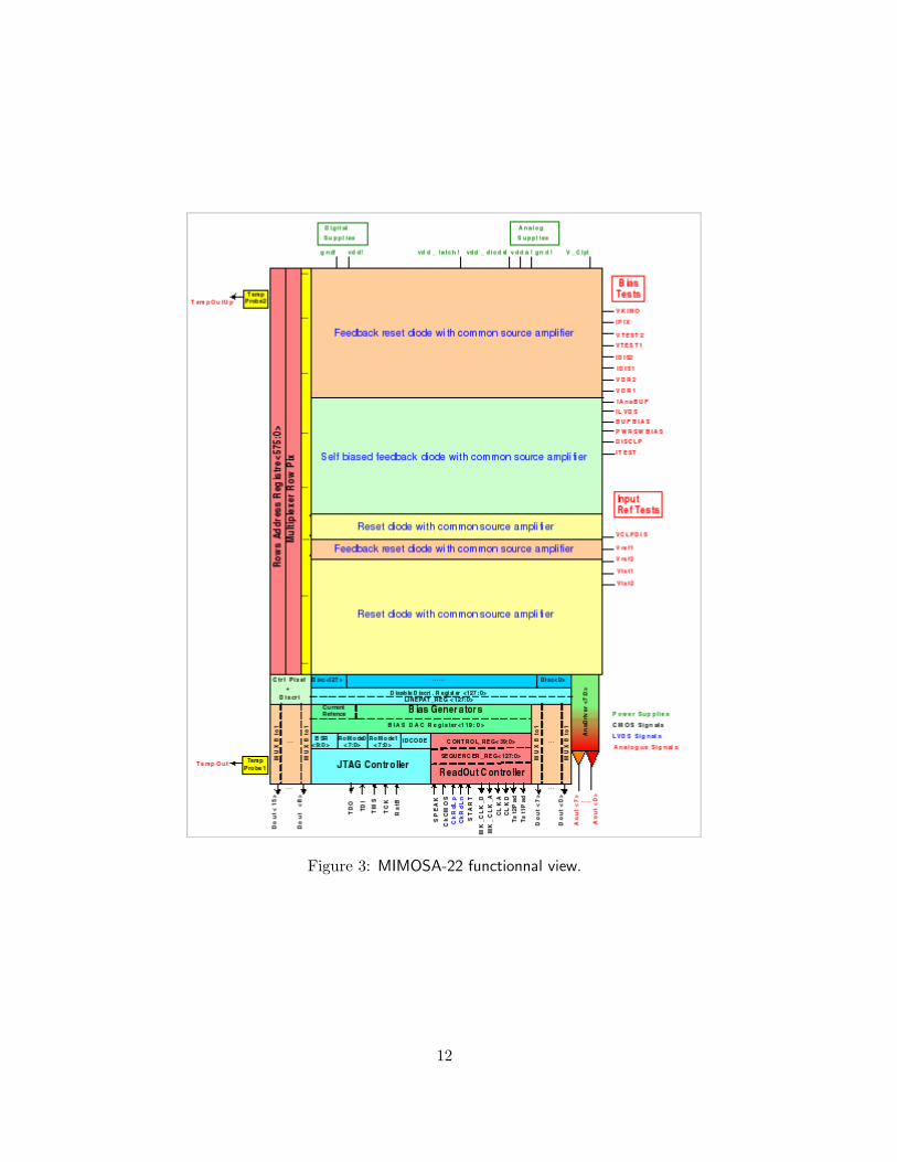
Figure 3: MIMOSA-22 functionnal view.
12
– the temporal (i.e. pixel) noise was found to be between ∼ 10 and ∼ 14 e−ENC6,depending on the sub-array studied;
– the Fixed Pattern Noise (FPN), reflecting the dispersion of the pixel characteristicsbelonging to the same column, was measured to be ∼ 5–6 e−ENC;
– the pixels featuring a design protecting the collection diode against the side-effectsof intense ionising radiation doses exhibited a temporal noise value exceeding thenoise of standard pixels by only ∼ 1 e−ENC;
– a modest temperature dependence of the total noise was observed. Its increaseamounted to . 10 % when ramping the chip operation temperature from +10◦Cto +35◦C;
• The charge collection efficiency was observed to be ∼ 70–80 % for a 3x3 pixel cluster,depending on the sub-array. Its value was found to be ∼ 80–90 % for 5x5 pixel clusters;
• No significant variation in the detection response over the sensitive area was observed;
• These results were derived from 5 different chips, which exhibited the same measurementresults within ± 5 %.
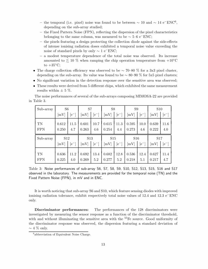
The noise performances of several of the sub-arrays composing MIMOSA-22 are providedin Table 3.
Sub-array S6 S7 S8 S9 S10
[mV] [e−] [mV] [e−] [mV] [e−] [mV] [e−] [mV] [e−]
TN 0.612 11.5 0.601 10.7 0.615 11.3 0.595 10.0 0.639 11.6
FPN 0.250 4.7 0.263 4.6 0.254 4.4 0.273 4.6 0.222 4.0
Sub-array S12 S13 S15 S16 S17
[mV] [e−] [mV] [e−] [mV] [e−] [mV] [e−] [mV] [e−]
TN 0.636 11.2 0.692 13.4 0.682 12.8 0.536 12.4 0.627 11.4
FPN 0.225 4.0 0.269 5.2 0.277 5.2 0.218 5.1 0.217 4.7
Table 3: Noise performances of sub-array S6, S7, S8, S9, S10, S12, S13, S15, S16 and S17observed in the laboratory. The measurements are provided for the temporal noise (TN) and theFixed Pattern Noise (FPN), in mV and in ENC.
It is worth noticing that sub-array S6 and S10, which feature sensing diodes with improvedionising radiation tolerance, exhibit respectively total noise values of 12.4 and 12.3 e−ENConly.
Discriminator performances: The performances of the 128 discriminators wereinvestigated by measuring the sensor response as a function of the discriminator threshold,with and without illuminating the sensitive area with the 55Fe source. Good uniformity ofthe discriminator response was observed, the dispersion featuring a standard deviation of∼ 4 % only.
6abbreviation of Equivalent Noise Charge.
13
hRTNEntries 2345Mean 12.47RMS 1.282Underflow 0Overflow 0
Electrons
0 10 20 30 40 50 60
1
10
210
310
hRTNEntries 2345Mean 12.47RMS 1.282Underflow 0Overflow 0
Seed pixel noise for real track cluster hsncEntries 2345Mean 28.53RMS 18.19Underflow 0Overflow 0
/ ndf 2χ 101.8 / 101Constant 17.1± 531.9 MPV 0.20± 17.55 Sigma 0.112± 4.369
Signal/Noise
0 20 40 60 80 100 120
Eve
nts
0
20
40
60
80
100
hsncEntries 2345Mean 28.53RMS 18.19Underflow 0Overflow 0
/ ndf 2χ 101.8 / 101Constant 17.1± 531.9 MPV 0.20± 17.55 Sigma 0.112± 4.369
S/N seed optimized hsncEntries 1211Mean 27.31RMS 18.15Underflow 0Overflow 0
/ ndf 2χ 58.18 / 90Constant 12.1± 281.8 MPV 0.3± 16.5 Sigma 0.144± 4.285
Signal/Noise
0 20 40 60 80 100 120
Eve
nts
0
10
20
30
40
50
hsncEntries 1211Mean 27.31RMS 18.15Underflow 0Overflow 0
/ ndf 2χ 58.18 / 90Constant 12.1± 281.8 MPV 0.3± 16.5 Sigma 0.144± 4.285
S/N seed optimized
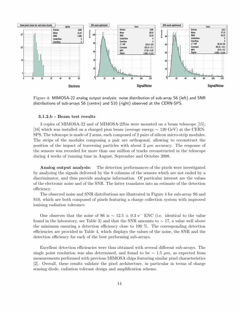
Figure 4: MIMOSA-22 analog output analysis: noise distribution of sub-array S6 (left) and SNRdistributions of sub-arrays S6 (centre) and S10 (right) observed at the CERN-SPS.
3.1.2.b - Beam test results
3 copies of MIMOSA-22 and of MIMOSA-22bis were mounted on a beam telescope [15],[16] which was installed on a charged pion beam (average energy ∼ 120 GeV) at the CERN-SPS. The telescope is made of 2 arms, each composed of 2 pairs of silicon micro-strip modules.The strips of the modules composing a pair are orthogonal, allowing to reconstruct theposition of the impact of traversing particles with about 2 µm accuracy. The response ofthe sensors was recorded for more than one million of tracks reconstructed in the telescopeduring 4 weeks of running time in August, Septembre and Octobre 2008.
Analog output analysis: The detection performances of the pixels were investigatedby analysing the signals delivered by the 8 columns of the sensors which are not ended by adiscriminator, and thus provide analogue information. Of particular interest are the valuesof the electronic noise and of the SNR. The latter translates into an estimate of the detectionefficiency.
The observed noise and SNR distributions are illustrated in Figure 4 for sub-array S6 andS10, which are both composed of pixels featuring a charge collection system with improvedionising radiation tolerance.
One observes that the noise of S6 is ∼ 12.5 ± 0.3 e− ENC (i.e. identical to the valuefound in the laboratory, see Table 3) and that the SNR amounts to ∼ 17, a value well abovethe minimum ensuring a detection efficiency close to 100 %. The corresponding detectionefficiencies are provided in Table 4, which displays the values of the noise, the SNR and thedetection efficiency for each of the best performing sub-arrays.
Excellent detection efficiencies were thus obtained with several different sub-arrays. Thesingle point resolution was also determined, and found to be ∼ 1.5 µm, as expected frommeasurements performed with previous MIMOSA chips featuring similar pixel characteristics[2]. Overall, these results validate the pixel architecture, in particular in terms of chargesensing diode, radiation tolerant design and amplification scheme.
14
Sub-array S6 S7 S8 S9 S10 S12 S13
Det. eff. 99.93 99.95 100.00 100.00 99.87 100.00 100.00± 0.05 % ± 0.04 % +0/-0.30 % +0/-0.14 % ± 0.09 % +0/-0.08 % +0/-0.07 %
N (e−) 12.5 ± 0.1 11.6 ± 0.1 12.3 ± 0.1 10.6 ± 0.1 13.6 ± 0.1 12.1 ± 0.1 14.0 ± 0.1
SNR 17.6 ± 0.2 18.5 ± 0.2 20.9 ± 1.1 19.5 ± 0.5 16.5 ± 0.3 18.2 ± 0.3 16.0 ± 0.3
Table 4: Detection efficiency, pixel noise (N, in ENC) and SNR measured at the CERN-SPS witheach of the seven best performing sub-arrays (S6-13). The values quoted for the SNR are mostprobable values for the seed pixel of the signal clusters.
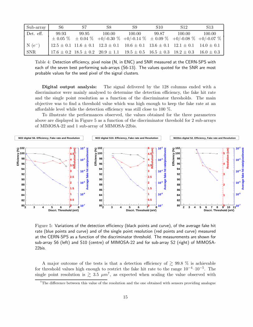
Digital output analysis: The signal delivered by the 128 columns ended with adiscriminator were mainly analysed to determine the detection efficiency, the fake hit rateand the single point resolution as a function of the discriminator thresholds. The mainobjective was to find a threshold value which was high enough to keep the fake rate at anaffordable level while the detection efficiency was still close to 100 %.
To illustrate the performances observed, the values obtained for the three parametresabove are displayed in Figure 5 as a function of the discriminator threshold for 2 sub-arraysof MIMOSA-22 and 1 sub-array of MIMOSA-22bis.
Discri. Threshold (mV)2 3 4 5 6 7 8
Effi
cien
cy (%
)
80
82
84
86
88
90
92
94
96
98
100
102
Res
olut
ion
(um
)
0
0.5
1
1.5
2
2.5
3
3.5
4
4.5
5
Ave
rage
fake
hit
rate
/pix
el/e
vent
-710
-610
-510
-410
-310
-210
M22 digital S6. Efficiency, Fake rate and Resolution
Discri. Threshold (mV)2 3 4 5 6 7 8
Effi
cien
cy (%
)
80
82
84
86
88
90
92
94
96
98
100
102R
esol
utio
n (u
m)
0
0.5
1
1.5
2
2.5
3
3.5
4
4.5
5
Ave
rage
fake
hit
rate
/pix
el/e
vent
-710
-610
-510
-410
-310
-210
M22 digital S10. Efficiency, Fake rate and Resolution
Discri. Threshold (mV)2 3 4 5 6 7 8 9 10 11
Effi
cien
cy (%
)
80
82
84
86
88
90
92
94
96
98
100
102
Res
olut
ion
(um
)
0
1
2
3
4
5
Ave
rage
fake
hit
rate
/pix
el/e
vent
-710
-610
-510
-410
-310
-210
M22bis digital S2. Efficiency, Fake rate and Resolution
Figure 5: Variations of the detection efficiency (black points and curve), of the average fake hitrate (blue points and curve) and of the single point resolution (red points and curve) measuredat the CERN-SPS as a function of the discriminator threshold. The measurements are shown forsub-array S6 (left) and S10 (centre) of MIMOSA-22 and for sub-array S2 (right) of MIMOSA-22bis.
A major outcome of the tests is that a detection efficiency of & 99.8 % is achievablefor threshold values high enough to restrict the fake hit rate to the range 10−4–10−5. Thesingle point resolution is & 3.5 µm7, as expected when scaling the value observed with
7The difference between this value of the resolution and the one obtained with sensors providing analogue
15
MIMOSA-16 linearly with the pixel pitch (i.e. from 25 to 18.4 µm). Finally, no performancenon-uniformity was observed over the chip surface, and all chips tested featured very similarperformances. Overall, these beam tests have shown that the sensor pixel and columnarchitectures are viable at real scale. Several sub-arrays (i.e. pixel designs) exhibit verysimilar performances. The choice of the best suited pixel design had to account for theradiation tolerance assessments, which are exposed in the next section.
3.1.3 Improvement and assessment of the radiation tolerance
3.1.3.a - Introductory remarks
The radiation tolerance of MIMOSA sensors was already assessed with several prototypes,as reported at previous PRC reviews. The observed tolerance to non-ionising radiation wasabout 2×10¹² neq/cm
2 for a 20 µm pitch sensor, and about 5 times as much for a 10 µm pitch.A satisfactory tolerance to ionising radiation was measured for integrated doses ranging upto 1 MRad [17], with sensors featuring a specific pixel design, optimised to deam the increaseof leakage current reaching the sensing diodes.
The overall conclusion is that the fluence expected at the ILC is not going to deterio-rate significantly the sensors and that their charge collection system can be adapted to therequired ionising radiation tolerance.
The sensors used for these studies did not feature integrated signal processing, i.e.they did not include in-pixel pre-amplification and CDS micro-circuits. The sensitivity ofMIMOSA-22 to ionising radiation needed therefore to be investigated.
3.1.3.b - Laboratory tests
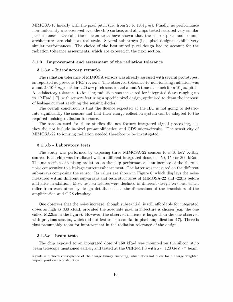
The study was performed by exposing three MIMOSA-22 sensors to a 10 keV X-Raysource. Each chip was irradiated with a different integrated dose, i.e. 50, 150 or 300 kRad.The main effect of ionising radiation on the chip performance is an increase of the thermalnoise consecutive to a leakage current enhancement. The latter was measured on the differentsub-arrays composing the sensor. Its values are shown in Figure 6, which displays the noisemeasured within different sub-arrays and tests structures of MIMOSA-22 and -22bis beforeand after irradiation. Most test structures were declined in different design versions, whichdiffer from each other by design details such as the dimensions of the transistors of theamplification and CDS circuitry.
One observes that the noise increase, though substantial, is still affordable for integrateddoses as high as 300 kRad, provided the adequate pixel architecture is chosen (e.g. the onecalled M22bis in the figure). However, the observed increase is larger than the one observedwith previous sensors, which did not feature substantial in-pixel amplification [17]. There isthus presumably room for improvement in the radiation tolerance of the design.
3.1.3.c - beam tests
The chip exposed to an integrated dose of 150 kRad was mounted on the silicon stripbeam telescope mentioned earlier, and tested at the CERN-SPS with a ∼ 120 GeV π− beam.
signals is a direct consequence of the charge binary encoding, which does not allow for a charge weightedimpact position reconstruction.
16
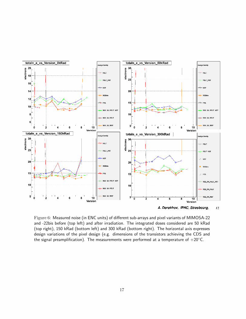
Figure 6: Measured noise (in ENC units) of different sub-arrays and pixel variants of MIMOSA-22and -22bis before (top left) and after irradiation. The integrated doses considered are 50 kRad(top right), 150 kRad (bottom left) and 300 kRad (bottom right). The horizontal axis expressesdesign variations of the pixel design (e.g. dimensions of the transistors achieving the CDS andthe signal preamplification). The measurements were performed at a temperature of +20◦C.
17
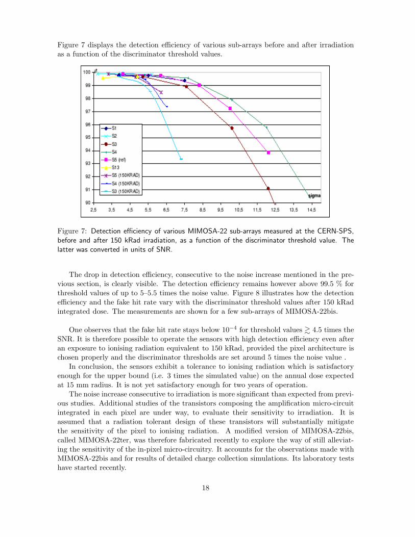
Figure 7 displays the detection efficiency of various sub-arrays before and after irradiationas a function of the discriminator threshold values.
Figure 7: Detection efficiency of various MIMOSA-22 sub-arrays measured at the CERN-SPS,before and after 150 kRad irradiation, as a function of the discriminator threshold value. Thelatter was converted in units of SNR.
The drop in detection efficiency, consecutive to the noise increase mentioned in the pre-vious section, is clearly visible. The detection efficiency remains however above 99.5 % forthreshold values of up to 5–5.5 times the noise value. Figure 8 illustrates how the detectionefficiency and the fake hit rate vary with the discriminator threshold values after 150 kRadintegrated dose. The measurements are shown for a few sub-arrays of MIMOSA-22bis.
One observes that the fake hit rate stays below 10−4 for threshold values & 4.5 times theSNR. It is therefore possible to operate the sensors with high detection efficiency even afteran exposure to ionising radiation equivalent to 150 kRad, provided the pixel architecture ischosen properly and the discriminator thresholds are set around 5 times the noise value .
In conclusion, the sensors exhibit a tolerance to ionising radiation which is satisfactoryenough for the upper bound (i.e. 3 times the simulated value) on the annual dose expectedat 15 mm radius. It is not yet satisfactory enough for two years of operation.
The noise increase consecutive to irradiation is more significant than expected from previ-ous studies. Additional studies of the transistors composing the amplification micro-circuitintegrated in each pixel are under way, to evaluate their sensitivity to irradiation. It isassumed that a radiation tolerant design of these transistors will substantially mitigatethe sensitivity of the pixel to ionising radiation. A modified version of MIMOSA-22bis,called MIMOSA-22ter, was therefore fabricated recently to explore the way of still alleviat-ing the sensitivity of the in-pixel micro-circuitry. It accounts for the observations made withMIMOSA-22bis and for results of detailed charge collection simulations. Its laboratory testshave started recently.
18
S/N3 4 5 6 7 8
Effic
iency
(%)
90
92
94
96
98
100
FELT+Vst2m µS1 11.3
2m µS2 11.3
FELT+Vst2m µS3 14.6
FELT2m µS4 14.6
ref Mi222m µS5 14.6
M22bis digital Efficiency after 150kRad
S/N3 4 5 6 7 8
Aver
age
fake
hit r
ate/
pixel/
even
t
-610
-510
-410
-310
-210 FELT+Vst2m µS1 11.3
2m µS2 11.3
FELT+Vst2m µS3 14.6
FELT2m µS4 14.6
ref Mi222m µS5 14.6
M22bis digital fake hit rate
Figure 8: Detection efficiency (left) and fake hit rate (right) as a function of discriminatorthreshold measured on a ∼ 120 GeV π− beam at the CERN-SPS for a MIMOSA-22bis sensorexposed to 150 kRad integrated dose. The chip response is displayed for various sub-arrays. Thethreshold values are expressed in SNR units.
Finally, one should keep in mind that the leakage current increase generated by ionisingradiation is quite closely related to the fabrication technology of the sensors. The processwhich would be used for sensors really equipping an ILC vertex detector would exhibit afeature size substantially shorter than the 0.35 µm of the process used for the chip develop-ment. This smaller feature size is expected to act directly on the sensor tolerance to ionisingradiation. Overall, it is therefore likely that the MIMOSA-22 pixel architecture is suited tothe most pessimistic radiation level scenario envisaged today for an ILC vertex detector.
3.2 Zero-suppression micro-circuit SUZE-01
This chip features the micro-circuits allowing to select those pixels of a frame having collecteda signal charge superior to the discriminator threshold. The consecutive data flow reductionwill allow running the vertex detector with high particle rates.
The chip was fabricated in 2007, mainly composed of zero-suppression micro-circuitscombined with output memories [18]. Its logic features two consecutives steps. The first oneaddresses groups of 64 columns and considers up to 6 series of ≤ 4 consecutive pixels hit ina row. When selecting a group of pixels, it provides their address in a compact way whichminimises the size of the information transmitted to the second level of the logic. The lattercombines the results of the logic attached to the different groups of 64 columns. SUZE-01 isrestricted to 2 groups of 64 columns. The encoded information delivered by the logic feedsan output memory. The memories are duplicated in ordre to allow simultaneous writing inone memory, while the neighbouring one is being read out from the outside world. Figure 9displays the layout of the chip.
The chip functionnality tests started in 2007 and continued until Spring 2008 in ordre to
19
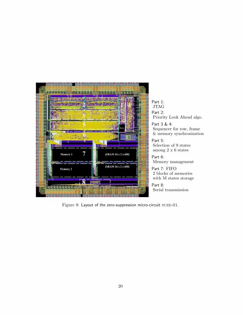
Figure 9: Layout of the zero-suppression micro-circuit suze-01.
Part 1:JTAG
Part 2:Priority Look Ahead algo.
Part 3 & 4:Sequencer for row, frame& memory synchronisation
Part 5:Selection of 9 statesamong 2 x 6 states
Part 6:Memory management
Part 7: FIFO2 blocks of memorieswith M states storage
Part 8:Serial transmission
20
investigate its response to a large variety of pixel patterns. The tests demonstrated that thepixel selection and information encoding are fully operational. They work as expected up toclock frequencies as high as 115 MHz, i.e. 1.15 times the nominal frequency. These resultsvalidate the architecture for its integration in the MIMOSA-26 design.
3.3 Full scale sensor MIMOSA-26
Based on the results of the MIMOSA-22/-22bis and SUZE-01 prototypes, the full scale sensorMIMOSA-26 was fabricated at the beginning of 2009 in the same 0.35 µm technology.
3.3.1 Description of the sensor
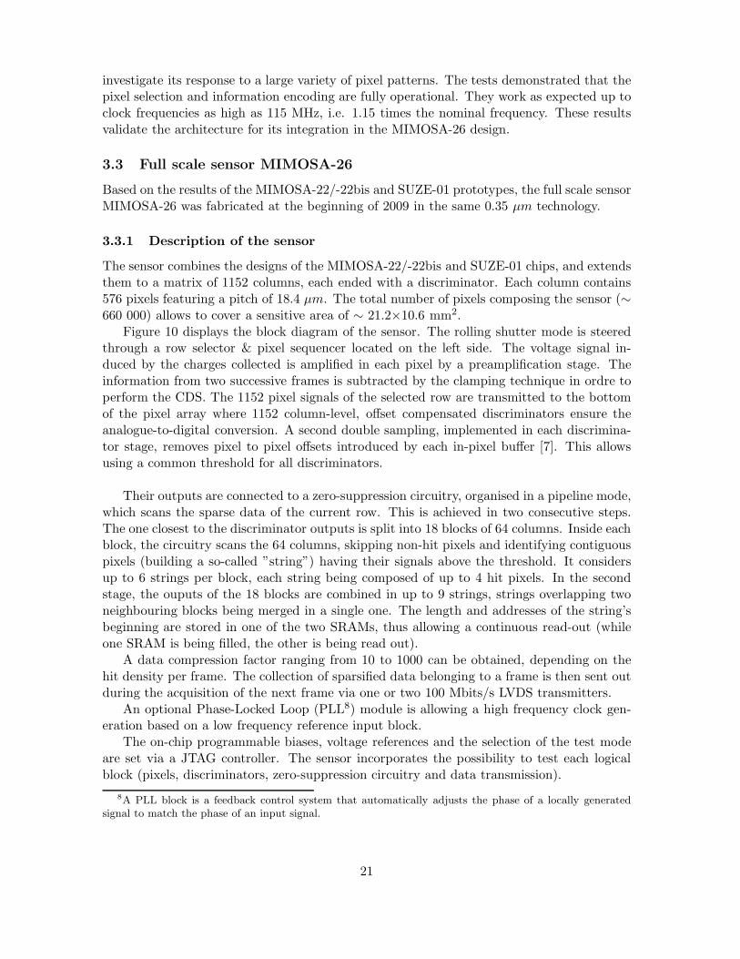
The sensor combines the designs of the MIMOSA-22/-22bis and SUZE-01 chips, and extendsthem to a matrix of 1152 columns, each ended with a discriminator. Each column contains576 pixels featuring a pitch of 18.4 µm. The total number of pixels composing the sensor (∼660 000) allows to cover a sensitive area of ∼ 21.2×10.6 mm2.
Figure 10 displays the block diagram of the sensor. The rolling shutter mode is steeredthrough a row selector & pixel sequencer located on the left side. The voltage signal in-duced by the charges collected is amplified in each pixel by a preamplification stage. Theinformation from two successive frames is subtracted by the clamping technique in ordre toperform the CDS. The 1152 pixel signals of the selected row are transmitted to the bottomof the pixel array where 1152 column-level, offset compensated discriminators ensure theanalogue-to-digital conversion. A second double sampling, implemented in each discrimina-tor stage, removes pixel to pixel offsets introduced by each in-pixel buffer [7]. This allowsusing a common threshold for all discriminators.
Their outputs are connected to a zero-suppression circuitry, organised in a pipeline mode,which scans the sparse data of the current row. This is achieved in two consecutive steps.The one closest to the discriminator outputs is split into 18 blocks of 64 columns. Inside eachblock, the circuitry scans the 64 columns, skipping non-hit pixels and identifying contiguouspixels (building a so-called ”string”) having their signals above the threshold. It considersup to 6 strings per block, each string being composed of up to 4 hit pixels. In the secondstage, the ouputs of the 18 blocks are combined in up to 9 strings, strings overlapping twoneighbouring blocks being merged in a single one. The length and addresses of the string’sbeginning are stored in one of the two SRAMs, thus allowing a continuous read-out (whileone SRAM is being filled, the other is being read out).
A data compression factor ranging from 10 to 1000 can be obtained, depending on thehit density per frame. The collection of sparsified data belonging to a frame is then sent outduring the acquisition of the next frame via one or two 100 Mbits/s LVDS transmitters.
An optional Phase-Locked Loop (PLL8) module is allowing a high frequency clock gen-eration based on a low frequency reference input block.
The on-chip programmable biases, voltage references and the selection of the test modeare set via a JTAG controller. The sensor incorporates the possibility to test each logicalblock (pixels, discriminators, zero-suppression circuitry and data transmission).
8A PLL block is a feedback control system that automatically adjusts the phase of a locally generatedsignal to match the phase of an input signal.
21
Column-level Discriminator
Selectable analogue outputs ~ 200 µm
Zero Suppression
Pad Ring
Pixel Array
1152 x 576
~300
0 µm
Row
sele
ctor
+ P
ixel s
eque
ncer
(~35
0 µm
)
~21.5 mm
~13.
8 m
mMemory 1 Memory 2 Bias DACJTAG Seq. Ctrl. PLL Test Block
Figure 10: Block-diagram of the MIMOSA-26 sensor, foreseen to equip the EUDET beamtelescope. The uniform green surface stands for the sensitive area. The signal processing circuitryis integrated at the chip periphery visible at the bottom, complemented with a narrow, < 400µm wide, vertical band visible on the left, used for the row by row addressing. A ∼ 200 µmwide band along the top of the picture contains the circuitry achieving the (slow) read-out of thepixels for their individual functionnality tests.
22
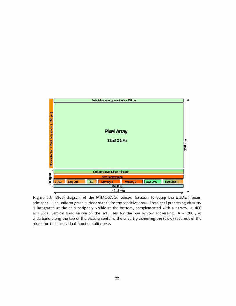
The sensor read-out time reflects the number of pixels per column and the pixel read-outsequence parametres. The read-out of each pixel requires 16 clock cycles at a frequencyof 80 MHz, i.e. 200 ns. A total time of 112.5 µs is thus required to read out the fullmatrix, accounting for a total number of 576 pixels per column. The clock frequency maybe increased by up to 50% in future.
3.3.2 Characterisation of MIMOSA-26
3.3.2.a - Introductory remarks
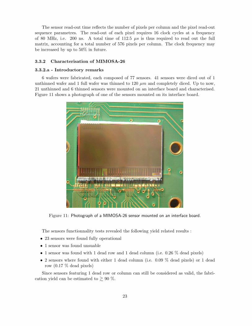
6 wafers were fabricated, each composed of 77 sensors. 41 sensors were diced out of 1unthinned wafer and 1 full wafer was thinned to 120 µm and completely diced. Up to now,21 unthinned and 6 thinned sensors were mounted on an interface board and characterised.Figure 11 shows a photograph of one of the sensors mounted on its interface board.
Figure 11: Photograph of a MIMOSA-26 sensor mounted on an interface board.
The sensors functionnality tests revealed the following yield related results :
• 23 sensors were found fully operational
• 1 sensor was found unsuable
• 1 sensor was found with 1 dead row and 1 dead column (i.e. 0.26 % dead pixels)
• 2 sensors where found with either 1 dead column (i.e. 0.09 % dead pixels) or 1 deadrow (0.17 % dead pixels)
Since sensors featuring 1 dead row or column can still be considered as valid, the fabri-cation yield can be estimated to & 90 %.
23
The sensors were tested extensively in the laboratory. The tests were first performedwith the analog part in ordre to check the pixel response over the complete sensitive area.Next the digital outputs were tested, in 4 different configurations:
• 1152 discriminators alone (isolated from the pixel array)
• all discriminators connected to the pixel array
• zero-suppression circuitry alone
• full chain including the pixel array, the discriminators and the zero-suppression logic.
The chip operation was started with a slightly slower read-out than the one of MIMOSA-22, because of the large number of discriminators (1152) working in parallel. The initial frameread-out frequency was set to ∼ 9 000 frames per second. It will be increased progressively,once it will have been checked that the discriminators stay all well synchronised and providea well controled uniform threshold value. The ultimate operation speed will thus be reachedafter the sensor commissioning.
The sensors are still being tested. Some of the main results obtained up to now aresummarised in this sub-section.
3.3.2.b - Tests of the analog part of the sensor
The analogue response was studied on 8 different sensors in ordre to evaluate the pixelnoise, the charge collection efficiency and the uniformity of the response over the sensitivearea. All sensors exhibited very similar performances.
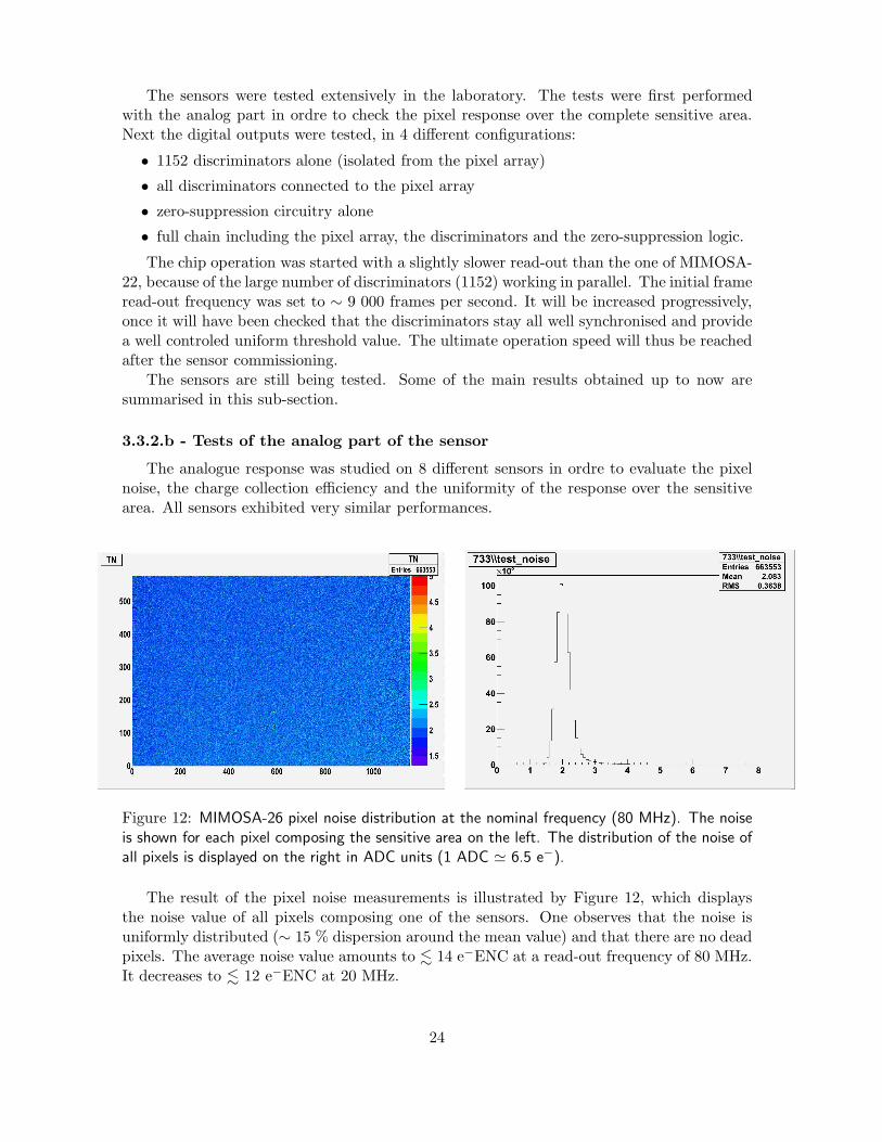
Figure 12: MIMOSA-26 pixel noise distribution at the nominal frequency (80 MHz). The noiseis shown for each pixel composing the sensitive area on the left. The distribution of the noise ofall pixels is displayed on the right in ADC units (1 ADC ≃ 6.5 e−).
The result of the pixel noise measurements is illustrated by Figure 12, which displaysthe noise value of all pixels composing one of the sensors. One observes that the noise isuniformly distributed (∼ 15 % dispersion around the mean value) and that there are no deadpixels. The average noise value amounts to . 14 e−ENC at a read-out frequency of 80 MHz.It decreases to . 12 e−ENC at 20 MHz.
24
The charge collection efficiency (CCE) was investigated by illuminating the sensors withan 55Fe source. The CCE was derived from the reconstructed clusters generated by the5.9 and 6.49 keV X-Rays. The measured values are shown in Table 5, where they arecompared to the CCE values observed with MIMOSA-22. The latter are well reproducedwith MIMOSA-269, which validates the extension of the MIMOSA-22 pixel design at fullscale.
Cluster size seed 2x2 3x3 5x5
MIMOSA-26 22 % 55 % 73 % 83 %
MIMOSA-22 22 % 58 % 75 % 86 %
Table 5: MIMOSA-26 CCE measurements compared to those of MIMOSA-22, when illuminatedwith an 55Fe source. The fraction of the cluster charge collected is displayed for the seed pixel(defined as the pixel having collected the largest charge in a cluster) and for clusters composedof 2×2, 3×3 and 5×5 pixels.
3.3.2.c - Tests of the digital part
The behaviour of the discriminators isolated from the pixel array was studied on 15unthinned and 6 thinned sensors. The steering of the discriminators being organised in4 groups, each addressing 288 contiguous columns, the noise performance was estimatedfor each group separately. The measurement consisted in estimating the response of thediscriminators to a fixed voltage by raising progressively their threshold.
The outcome of the study is illustrated in Figure 13, which displays the response ofa group of 288 discriminators as a function of the threshold value. One observes that alldiscriminators fire at low threshold and that a transition towards no firing occurs for voltagesabove -2 mV. The slope of the transition and its dispersion were interpreted in terms ofTemporal (TN) and Fixed Pattern Noise (FPN). The latter are shown in the middle and theright hand side of the figure. The TN amounts to ∼ 0.4 mV while the FPN is only ∼ 0.2mV, a modest value when compared to the pixel noise, which exceeds 0.5 mV. These resultsreproduce well the observations made with MIMOSA-22/-22bis (see sub-section 3.1.2.a), andshow that all discriminators are fully operational at nominal read-out frequency.
Next the discriminators were connected to the pixel array. The chip response was assessedat 80 MHz (112.5 µs frame read-out time) with the 15+6 sensors mentioned earlier. 4 sensorswere also studied at a read-out frequency of 20 MHz. The noise measurements performedwith isolated discriminators were repeated with each group of 288 connected discriminators.The values observed are shown for one group in Figure 14.
The total TN amounts to ∼ 0.6–0.7 mV, which is basically the value of the pixel TN.The total FPN amounts to ∼ 0.2–0.3 mV, which is dominated by the discriminator contri-bution. These values remain nearly constant when varying the read-out frequency from 80to 20 MHz. The conclusion of the tests at this stage is that the complete array reproducesthe performances extrapolated from the MIMOSA-22 prototype (see Table 3).
9The residual differences are compatible with sensor to sensor variations.
25
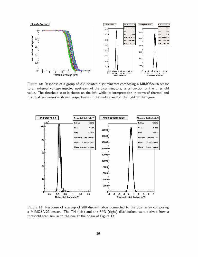
Figure 13: Response of a group of 288 isolated discriminators composing a MIMOSA-26 sensorto an external voltage injected upstream of the discriminators, as a function of the thresholdvalue. The threshold scan is shown on the left, while its interpretation in terms of thermal andfixed pattern noises is shown, respectively, in the middle and on the right of the figure.
Figure 14: Response of a group of 288 discriminators connected to the pixel array composinga MIMOSA-26 sensor. The TN (left) and the FPN (right) distributions were derived from athreshold scan similar to the one at the origin of Figure 13.
26
Next, the zero-suppression logic was investigated, disconnected from the rest of the chip.Various patterns were emulated with a pattern generator, and ran through the logic millionsof times without any error up to frequencies of 115 MHz (i.e. 1.15 times the nominalfrequency). All critical configurations, e.g. with strings overlapping two contiguous blocks,were checked repeatedly to be treated properly.
Finally, the signal processing of the complete chain, ranging from the pixel array to theoutput of the zero-suppression logic, was characterised on several different sensors. Theiroutput was studied in absence of any radiation source in ordre to evaluate the fake hit ratedue to noise fluctuations as a function of the discriminator threshold. Table 6 summarisesthe results.
Discriminator threshold 4 N 5 N 5.5 N 6 N 8 N 10 N
Npix > threshold (10−4) . 8 ∼ 1.5 ∼ 1 0.5 0.1 0.03
Table 6: Fake hit rate of a MIMOSA-26 sensor measured as a function of the discriminatorthresholds, in absence of radiation source (noise run).
One observes that discriminator threshold values ranging from 5 to 5.5 times the noisevalue allow maintaining the fake hit rate at a level of 10−4 (i.e. < pixels per frame). Thisresult remains essentially unchanged when varying the operation temperature from +20◦Cto +40◦C. It was also checked that multi-hit frames translate into the right output memorypatterns.
Finally, the power consumption of the sensor was measured. The static contribution isin the ordre of 600 mW, i.e. . 300 mW/cm2. This value compares well to the consumptionestimated per column, of ∼ 500 µW . The latter value is almost equally distributed betweenthe pixels (∼ 200 µW ) and the discriminators (. 300 µW ). The total dynamic powerconsumption was estimated to be in the ordre of 200 mW for an occupancy of ∼ 1 %.
3.3.2.d - Beam tests results
From July to Octobre 2009, MIMOSA-26 was operated 3 times on particle beams at theCERN-SPS. Part of these beam periods were devoted to the integration of the sensors in theEUDET beam telescope, where they are supposed to equip all planes of the final telescopeversion. Separate beam tests were performed to evaluate the sensor performances.
The tests started with a set of 3 sensors introduced as Device Under Test (DUT) inthe EUDET telescope demonstrator. The 3 sensors were operated synchronously and thetrack reconstruction was running smoothly after only a few days of run. The next step ofthe EUDET programme consisted in replacing all 6 analog output sensors composing thetelescope demonstrator with MIMOSA-26 chips, which are > 10 times faster and 4 timeslarger. The complete telescope was commissionned in Septembre 2009 with & 100 GeV pionsat the CERN-SPS.
6 other sensors, some of them thinned to 120 µm, were combined to build another tele-scope, which was installed at the CERN-SPS for the sensor assessment. They were operatedduring about 10 days with & 100 GeV pions and their response to the beam particles werestudied as a function of the discriminator threshold value.
27
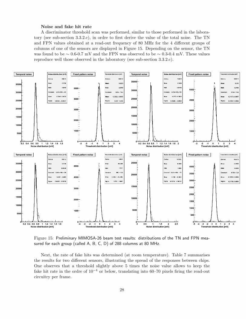
Noise and fake hit rateA discriminator threshold scan was performed, similar to those performed in the labora-
tory (see sub-section 3.3.2.c), in ordre to first derive the value of the total noise. The TNand FPN values obtained at a read-out frequency of 80 MHz for the 4 different groups ofcolumns of one of the sensors are displayed in Figure 15. Depending on the sensor, the TNwas found to be ∼ 0.6-0.7 mV and the FPN was observed to be ∼ 0.3-0.4 mV. These valuesreproduce well those observed in the laboratory (see sub-section 3.3.2.c).
Figure 15: Preliminary MIMOSA-26 beam test results: distributions of the TN and FPN mea-sured for each group (called A, B, C, D) of 288 columns at 80 MHz.
Next, the rate of fake hits was determined (at room temperature). Table 7 summarisesthe results for two different sensors, illustrating the spread of the responses between chips.One observes that a threshold slightly above 5 times the noise value allows to keep thefake hit rate in the ordre of 10−4 or below, translating into 60–70 pixels firing the read-outcircuitry per frame.
28
Discriminator threshold 5 N 6 N 7 N 8 N 10 N 12 N
Fake rate of chip Nr. 24 (10−4) 1.6 0.6 0.24 0.095 0.026 0.017
Fake rate of chip Nr. 1 (10−4) 3.3 1.2 – 0.23 0.054 –
Table 7: Preliminary MIMOSA-26 beam test results: values of the average fake hit rate due topixel noise fluctuations as a function of the discriminator threshold at 80 MHz. The latter areexpressed in units of the SNR. The fake rate is indicated in 10−4 units for two different sensors.
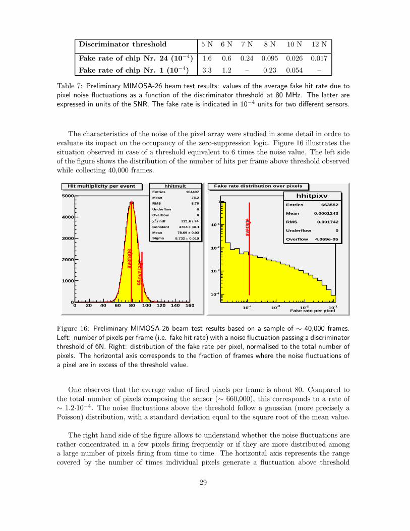
The characteristics of the noise of the pixel array were studied in some detail in ordre toevaluate its impact on the occupancy of the zero-suppression logic. Figure 16 illustrates thesituation observed in case of a threshold equivalent to 6 times the noise value. The left sideof the figure shows the distribution of the number of hits per frame above threshold observedwhile collecting 40,000 frames.
hhitmultEntries 104497
Mean 78.2
RMS 8.78
Underflow 0
Overflow 0
/ ndf 2χ 221.6 / 74
Constant 18.1± 4764
Mean 0.03± 78.69
Sigma 0.019± 8.732
0 20 40 60 80 100 120 140 1600
1000
2000
3000
4000
5000
hhitmultEntries 104497
Mean 78.2
RMS 8.78
Underflow 0
Overflow 0
/ ndf 2χ 221.6 / 74
Constant 18.1± 4764
Mean 0.03± 78.69
Sigma 0.019± 8.732
aver
age
95ov
erag
e
Hit multiplicity per event
hhitpixvEntries 663552
Mean 0.0001243
RMS 0.001742
Underflow 0
Overflow 4.069e-05
Fake rate per pixel-410
-310 -210 -110
-410
-310
-210
-110
1hhitpixv
Entries 663552
Mean 0.0001243
RMS 0.001742
Underflow 0
Overflow 4.069e-05
aver
age
Fake rate distribution over pixels
Figure 16: Preliminary MIMOSA-26 beam test results based on a sample of ∼ 40,000 frames.Left: number of pixels per frame (i.e. fake hit rate) with a noise fluctuation passing a discriminatorthreshold of 6N. Right: distribution of the fake rate per pixel, normalised to the total number ofpixels. The horizontal axis corresponds to the fraction of frames where the noise fluctuations ofa pixel are in excess of the threshold value.
One observes that the average value of fired pixels per frame is about 80. Compared tothe total number of pixels composing the sensor (∼ 660,000), this corresponds to a rate of∼ 1.2·10−4. The noise fluctuations above the threshold follow a gaussian (more precisely aPoisson) distribution, with a standard deviation equal to the square root of the mean value.
The right hand side of the figure allows to understand whether the noise fluctuations arerather concentrated in a few pixels firing frequently or if they are more distributed amonga large number of pixels firing from time to time. The horizontal axis represents the rangecovered by the number of times individual pixels generate a fluctuation above threshold
29
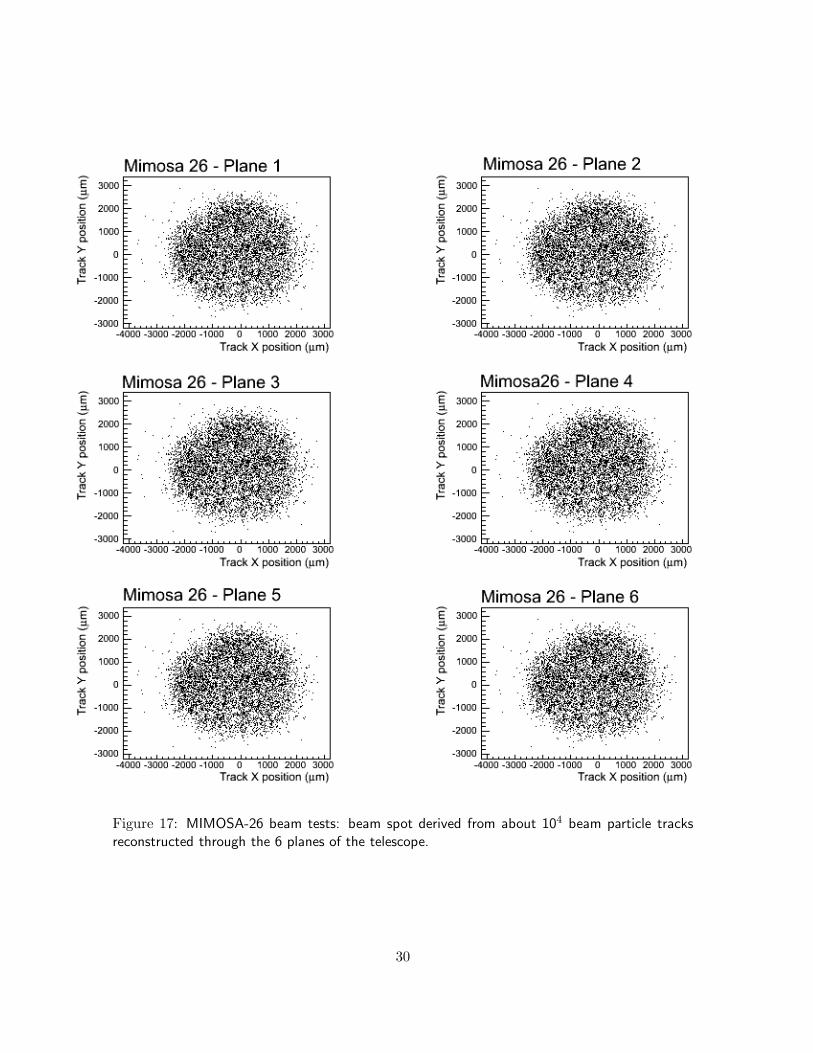
Figure 17: MIMOSA-26 beam tests: beam spot derived from about 104 beam particle tracksreconstructed through the 6 planes of the telescope.
30
within 40,000 frames. This number is actually displayed normalised to the number of framesin ordre to correspond to the fake rate. The vertical axis expresses the number of pixelshaving fired a given number of times. This number is shown normalised to the total numberof pixels. One observes that the majority of the pixels generates noise fluctuations abovethreshold at a rate (O(10−5) well below the average value (∼ 10−4), and that a relativelymodest fraction of the pixels generates most of the fake hits. For instance, a few per-mill ofthe pixels fire at least once every 100 frames due to their noise fluctuation. More statisticsis needed to evaluate how these values compare from one sensor to another.
Detection efficiencyThe detection efficiency was evaluated next for different threshold values and on different
sensors, together with the cluster multiplicity distribution and the single point resolution.The events collected were triggered with a 7×7 mm2 scintillator slab. Good quality trackswere reconstructed through the telescope for ∼ 80 % of the triggers. Figure 17 shows thedistribution of the particles’ impacts in each of the 6 sensors, providing an image of the beamspot based on about 10,000 reconstructed tracks. The correlation between the impacts indifferent planes is clearly visible.
Fake hit rate-710 -610 -510 -410 -310
effic
ienc
y (%
)
94
95
96
97
98
99
100
101
102Efficiency vs Fake hit rate
PRELIM
INARY
MIMOSA 22-S6
MIMOSA 22bis-S5
MIMOSA 26 (chip 1) unthinned, vref2=98, 80 MHz
Efficiency vs Fake hit rate
Threshold (/noise)2 4 6 8 10 12 14
Fak
e hi
t rat
e
-710
-610
-510
-410
-310
Fake hit rate vs Threshold
PRELIM
INARY
MIMOSA 22-S6
MIMOSA 22bis-S5
MIMOSA 26 (chip 1) unthinned, vref2=98, 80 MHz
MIMOSA 26 (chip 1) unthinned, vref2=118, 80 MHz
MIMOSA 26 (chip 24) thinned, vref2=98, 80 MHz
MIMOSA 26 (chip 24) thinned, vref2=98, 20 MHz
MIMOSA 26 (chip 1) unthinned, vref2=98, 20 MHz
Fake hit rate vs Threshold
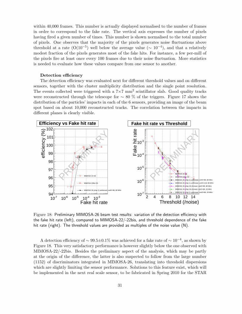
Figure 18: Preliminary MIMOSA-26 beam test results: variation of the detection efficiency withthe fake hit rate (left), compared to MIMOSA-22/-22bis, and threshold dependence of the fakehit rate (right). The threshold values are provided as multiples of the noise value (N).
A detection efficiency of ∼ 99.5±0.1% was achieved for a fake rate of ∼ 10−4, as shown byFigure 18. This very satisfactory performance is however slightly below the one observed withMIMOSA-22/-22bis. Besides the preliminary aspect of the analysis, which may be partlyat the origin of the difference, the latter is also suspected to follow from the large number(1152) of discriminators integrated in MIMOSA-26, translating into threshold dispersionswhich are slightly limiting the sensor performance. Solutions to this feature exist, which willbe implemented in the next real scale sensor, to be fabricated in Spring 2010 for the STAR
31
vertex detector.
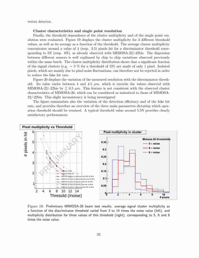
Cluster characteristics and single point resolutionFinally, the threshold dependence of the cluster multiplicity and of the single point res-
olution were evaluated. Figure 19 displays the cluster multiplicity for 3 different thresholdvalues, as well as its average as a function of the threshold. The average cluster multiplicityconcentrates around a value of 4 (resp. 3.5) pixels hit for a discriminator threshold corre-sponding to 5N (resp. 6N), as already observed with MIMOSA-22/-22bis. The dispersionbetween different sensors is well explianed by chip to chip variations observed previouslywithin the same batch. The cluster multiplicity distribution shows that a significant fractionof the signal clusters (e.g. ∼ 5 % for a threshold of 5N) are made of only 1 pixel. Isolatedpixels, which are mainly due to pixel noise fluctuations, can therefore not be rejected in ordreto reduce the fake hit rate.
Figure 20 displays the variation of the measured resolution with the discriminator thresh-old. Its value varies between 4 and 4.5 µm, which is exceeds the values observed withMIMOSA-22/-22bis by & 0.5 µm. This feature is not consistent with the observed clustercharacteristics of MIMOSA-26, which can be considered as indentical to those of MIMOSA-22/-22bis. This slight inconsistency is being investigated
The figure summarises also the variation of the detection efficiency and of the fake hitrate, and provides therefore an overview of the three main parametres dictating which oper-ation threshold should be retained. A typical threshold value around 5.5N provides clearlysatisfactory performances.
Thresold (/noise)2 4 6 8 10 12 14
# pi
xels
in h
it
1
2
3
4
5
6Pixel multiplicity vs Threshold
PRELIM
INARY
MIMOSA 22-S6
MIMOSA 22bis-S5
MIMOSA 26 (chip 1) unthinned, vref2=98, 80 MHz
MIMOSA 26 (chip 1) unthinned, vref2=118, 80 MHz
MIMOSA 26 (chip 24) thinned, vref2=98, 80 MHz
MIMOSA 26 (chip 24) thinned, vref2=98, 20 MHz
MIMOSA 26 (chip 1) unthinned, vref2=98, 20 MHz
Pixel multiplicity vs Threshold
Figure 19: Preliminary MIMOSA-26 beam test results: average signal cluster multiplicity asa function of the discriminator threshold varied from 3 to 14 times the noise value (left), andmultiplicity distribution for three values of this threshold (right), corresponding to 5, 6 and 8times the noise value.
32
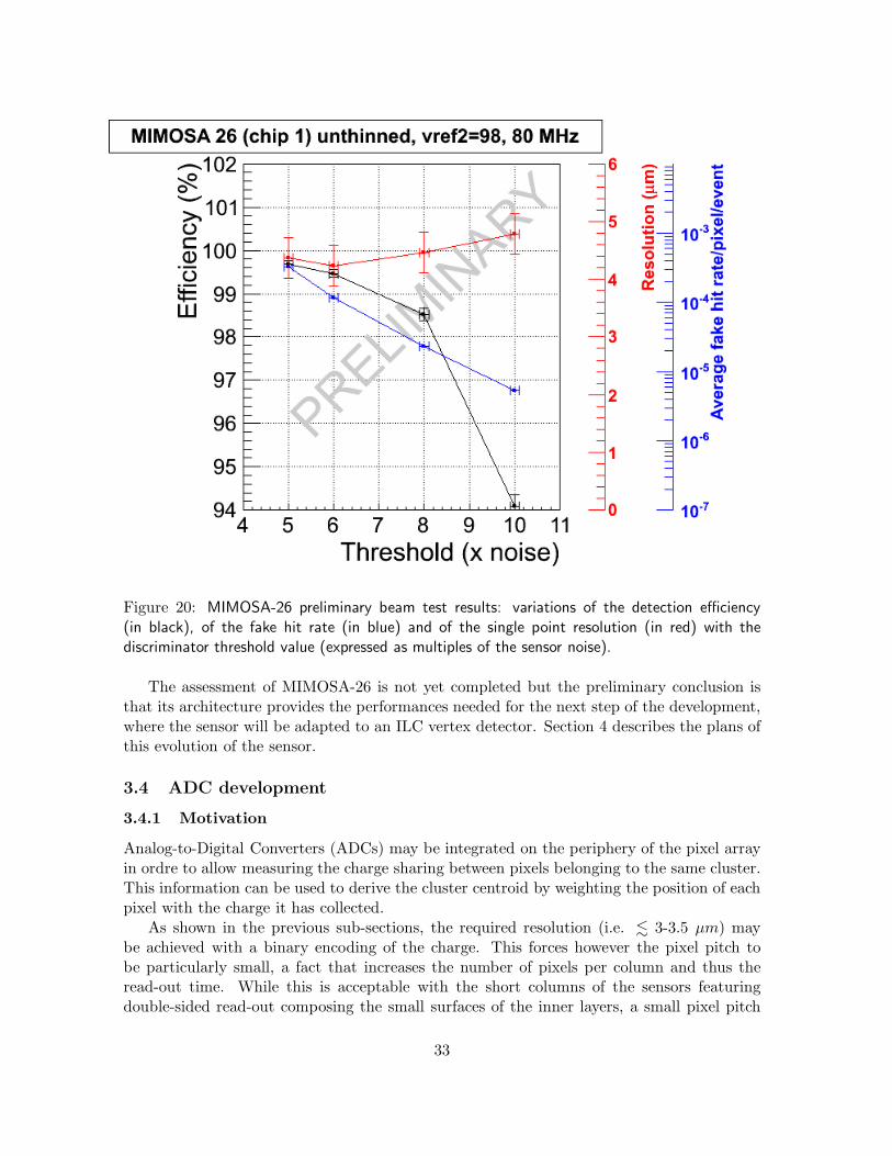
Figure 20: MIMOSA-26 preliminary beam test results: variations of the detection efficiency(in black), of the fake hit rate (in blue) and of the single point resolution (in red) with thediscriminator threshold value (expressed as multiples of the sensor noise).
The assessment of MIMOSA-26 is not yet completed but the preliminary conclusion isthat its architecture provides the performances needed for the next step of the development,where the sensor will be adapted to an ILC vertex detector. Section 4 describes the plans ofthis evolution of the sensor.
3.4 ADC development
3.4.1 Motivation
Analog-to-Digital Converters (ADCs) may be integrated on the periphery of the pixel arrayin ordre to allow measuring the charge sharing between pixels belonging to the same cluster.This information can be used to derive the cluster centroid by weighting the position of eachpixel with the charge it has collected.
As shown in the previous sub-sections, the required resolution (i.e. . 3-3.5 µm) maybe achieved with a binary encoding of the charge. This forces however the pixel pitch tobe particularly small, a fact that increases the number of pixels per column and thus theread-out time. While this is acceptable with the short columns of the sensors featuringdouble-sided read-out composing the small surfaces of the inner layers, a small pixel pitch
33
is less optimal for the outer layers. The pixel pitch is also not required to be as small sincethe occupancy is 1-2 ordres of magnitude smaller and since particles belonging to the samejet are farer apart.
A pitch of 30-35 µm is therefore foreseen in layers SL3-SL5 or DL2-3. The numberof pixels per (2 cm long) column allows then rather easily to read the sensor in . 100µs. By equipping each column with an ADC, a single point resolution of . 3 µm canbe achieved. This will allow reconstructing vertices of particles decaying inside the vertexdetector volume and ensures a good track linking with the peripheral detectors. Studiesperformed with sensors delivering analog signals encoded on 12 bits have shown that 3 bitsshould be enough for the value ambitioned, provided they are effective. It was consideredmore realistic to foresee 4 or 5 bits in ordre to face without harming the resolution thepotential disappearance of the first bit due to the ADC noise.
The development of ADCs is actually not only driven by the requirements for the outerlayers. It also accounts for the fact that the resolution requirements for the inner layer are notyet fully established because the studies supporting them did not address system integrationissues (e.g. alignment) and rely on physics simulations and final state reconstruction softwarewhich did not contain the degree of realism required for the task (e.g. distinguish between2 and 3 µm resolution). More detailed studies will be carried out in the coming years,which may show that a . 2 µm single point resolution improves significantly the physicsperformance of the vertex detector. Technical development addressing system integration anddetector operation in the near future could also lead to the evidence of a significant dilutionof the impact parametre resolution (e.g. due to residual missalignment), which could bepartly compensated with a more accurate sensor single point resolution. In perspective ofsuch potential cases, the MIMOSA architecture needs to be developed with the possibilitykept open to end each column with a low power and compact ADC, adapted to the sensorread-out frequency.
3.4.2 Prototyping achievements
Various ADC architecture options were prototyped in ordre to find the best combination ofthe three dominating performance constrains, i.e. speed, dimensions and power consumption.They exploit the fact that the impact position reconstruction is essentially insensitive tocharge deposits superior to the peak of the Landau distribution. This allows focussing theADC dynamical range on charge values below 10-15 times the noise value (i.e. . 200 e−).Two prototyping lines have made substantial progress since Spring 2007: they explore apipeline and a Wilkinson architecture. Their main results are summarised hereafter.
All prototypes were manufactured in a CMOS 0.35 µm technology in ordre to be com-patible with the sensor fabrication process. As a consequence, the performances obtainedgive a pessimistic figure of merit of each prototype, as compared to what could be extractedfrom processes with smaller feature size, like those envisaged for the final sensor production.
3.4.2.a - Pipeline ADC:Three consecutive pipeline ADC prototypes were fabricated since 2005, ending up with a
signal charge encoding micro-circuitry organised in 3 pipeline stages of 1.5 bits complementedwith a 2-bit flash stage. This structure, which was prototyped in 2007/2008, minimises theoffsets and the parasitic capacitance reflecting the inconvenient dimensions of the ADC,
34
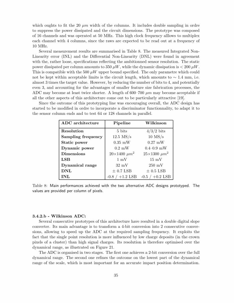
which oughts to fit the 20 µm width of the columns. It includes double sampling in ordreto suppress the power dissipated and the circuit dimensions. The prototype was composedof 16 channels and was operated at 50 MHz. This high clock frequency alllows to multiplexeach channel with 4 columns, since the raws are expected to be read out at a frequency of10 MHz.
Several measurement results are summarised in Table 8. The measured Integrated Non-Linearity error (INL) and the Differential Non-Linearity (DNL) were found in agreementwith the, rather loose, specifications reflecting the ambitionned sensor resolution. The staticpower dissipated per column amounts to 350 µW , while the dynamic dissipation is < 200 µW .This is compatible with the 500 µW upper bound specified. The only parametre which couldnot be kept within acceptable limits is the circuit length, which amounts to ∼ 1.4 mm, i.e.almost 3 times the target value. However, by reducing the number of bits to 4, and potentiallyeven 3, and accounting for the advantages of smaller feature size fabrication processes, theADC may become at least twice shorter. A length of 600–700 µm may become acceptable ifall the other aspects of this architecture come out to be particularly attractive [19].
Since the outcome of this prototyping line was encouraging overall, the ADC design hasstarted to be modified in ordre to incorporate a discriminator functionnality, to adapt it tothe sensor column ends and to test 64 or 128 channels in parallel.
ADC architecture Pipeline Wilkinson
Resolution 5 bits 4/3/2 bits
Sampling frequency 12.5 MS/s 10 MS/s
Static power 0.35 mW 0.27 mW
Dynamic power 0.2 mW 0.4–0.9 mW
Dimensions 20×1400 µm2 25×1300 µm2
LSB 1 mV 15 mV
Dynamical range 32 mV 250 mV
DNL ± 0.7 LSB ± 0.5 LSB
INL -0.8 / +1.2 LSB -0.5 / +0.2 LSB
Table 8: Main performances achieved with the two alternative ADC designs prototyped. Thevalues are provided per column of pixels.
3.4.2.b - Wilkinson ADC:Several consecutive prototypes of this architecture have resulted in a double digital slope
converter. Its main advantage is to transform a 4-bit conversion into 2 consecutive conver-sions, allowing to speed up the ADC at the required sampling frequency. It exploits thefact that the single point resolution is more influenced by low charge deposits (in the crownpixels of a cluster) than high signal charges. Its resolution is therefore optimised over thedynamical range, as illustrated on Figure 21.
The ADC is organised in two stages. The first one achieves a 2-bit conversion over the fulldynamical range. The second one refines the outcome on the lowest part of the dynamicalrange of the scale, which is most important for an accurate impact position determination.
35
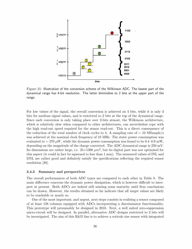
Figure 21: Illustration of the conversion scheme of the Wilkinson ADC. The lowest part of thedynamical range has 4-bit resolution. The latter diminishes to 2 bits at the upper part of therange.
For low values of the signal, the overall conversion is achieved on 4 bits, while it is only 3bits for medium signal values, and is restricted to 2 bits at the top of the dynamical range.Since each conversion is only taking place over 2-bits atmost, the Wilkinson architecture,which is relatively slow when compared to other architectures, can nevertheless cope withthe high read-out speed required for the sensor read-out. This is a direct consequence ofthe reduction of the total number of clock cycles to 4. A sampling rate of ∼ 10 MSample/swas achieved at the nominal clock frequency of 10 MHz. The static power consumption wasevaluated to ∼ 270 µW , while the dynamic power consumption was found to be 0.4–0.9 mW,depending on the magnitude of the charge converted. The ADC dynamical range is 250 mV.Its dimensions are rather large, i.e. 25×1300 µm2, but its digital part was not optimised forthis aspect (it could in fact be squeezed to less than 1 mm). The measured values of INL andDNL are rather good and definitely satisfy the specifications reflecting the required sensorresolution [20].
3.4.3 Summary and perspectives
The overall performances of both ADC types are compared to each other in Table 8. Themain difference concerns the dynamic power dissipation, which is however difficult to inter-pret at present. Both ADCs are indeed still missing some maturity until firm conclusionscan be drawn. However, the results obtained so far indicate that all target values are likelyto be reachable or nearly so.
One of the most important, and urgent, next steps consists in realising a sensor composedof at least 128 columns equipped with ADCs incorporating a discriminator functionnality.This prototype will presumably be designed in 2010. Next, a well suited zero-suppressionmicro-circuit will be designed. In parallel, alternative ADC designs restricted to 3 bits willbe investigated. The aim of this R&D line is to achieve a reticule size sensor with integrated
36
ADCs and zero-suppression by 2012.
4 Next steps of the sensor development
The main consequence of the satisfactory performances of MIMOSA-26 is that an architec-ture has been validated, which is likely to be further developed until it complies with allILD vertex detector specifications. To meet this goal, two types of improvements have to becarried out: those concerning generic imperfections of the sensors and those addressing theirspecific incomplete adequacy with the VTX requirements.
4.1 Generic improvements
The generic imperfections concern mainly the two insensitive side bands of the sensor incor-porating micro-circuits which cannot be implemented inside the pixel array.
The most embarrassing is the ∼ 350 µm side band parallel to the columns, which isneeded to steer the raws (see Figure 10). It introduces a dead zone inbetween neighbouringsensors on a ladder corresponding to & 1.5 % of the geometrical acceptance. One maythink of staggering the sensors, but this may complicate their integration substantially. Thesteering micro-circuits are not implemented on the pixel array because the present fabricationtechnology, which is only used for the R&D, does not allow for more than 4 metal layers(typical for a 0.35 µm CMOS technology). Since the final production would take place ina CMOS technology with at least twice smaller feature size, the limitation would disappearbecause at least 6 metal layers are usually available in these processes.
The other insensitive part of the sensors is the peripheral side band hosting the dis-criminators, the zero-suppression logic and the output memories. It is perpendicular to thecolumns and does therefore not affect the geometrical acceptance. It introduces howeversome additionnal material, though rather modest, inside the fiducial volume. The band ispresently ∼ 3 mm wide, translating into ∼ 0.03 % X0 additionnal material in the innermostlayer (assuming the sensors are thinned to . 40 µm and that they are read out from bothsides, as explained later in this document). In the final sensor design, trials will be made toshrink the width of the band to . 2 mm. A smaller CMOS process feature size will helpgoing into this direction. The main difficulty towards this goal may come from the size ofthe output memories, which have to accommodate the data flow generated by the high beamrelated background firing the pixels.
4.2 Specific performance improvements
The sensor R&D of the coming years will actually be governed by requirements which a morespecific to an ILC vertex detector. The most important parametre is the read-out speed,which needs to be improved by a factor of & 4 in the innermost layer. On the other hand, itis already suited to the outer layers, provided the pixel spitch is increased to 30-35 µm, andeach column gets terminated with an ADC incorporating a discriminator functionnality.
4.2.1 Adapting the sensors to the inner layer
Adapting the sensors to the inner layers will rely on two complementary approaches. The firstone will consist in subdividing the columns in two equal halves, read out on both sides of the
37
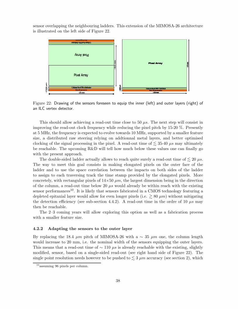
sensor overlapping the neighbouring ladders. This extension of the MIMOSA-26 architectureis illustrated on the left side of Figure 22.
Figure 22: Drawing of the sensors foreseen to equip the inner (left) and outer layers (right) ofan ILC vertex detector.
This should allow achieving a read-out time close to 50 µs. The next step will consist inimproving the read-out clock frequency while reducing the pixel pitch by 15-20 %. Presentlyat 5 MHz, the frequency is expected to evolve towards 10 MHz, supported by a smaller featuresize, a distributed raw steering relying on addtionnal metal layers, and better optimisedclocking of the signal processing in the pixel. A read-out time of . 35-40 µs may ultimatelybe reachable. The upcoming R&D will tell how much below these values one can finally gowith the present approach.
The double-sided ladder actually allows to reach quite surely a read-out time of . 20 µs.The way to meet this goal consists in making elongated pixels on the outer face of theladder and to use the space correlation between the impacts on both sides of the ladderto assign to each traversing track the time stamp provided by the elongated pixels. Moreconcretely, with rectangular pixels of 14×50 µm, the largest dimension being in the directionof the column, a read-out time below 20 µs would already be within reach with the existingsensor performances10. It is likely that sensors fabricated in a CMOS technology featuring adepleted epitaxial layer would allow for even longer pixels (i.e. & 80 µm) without mitigatingthe detection efficiency (see sub-section 4.4.2). A read-out time in the ordre of 10 µs maythen be reachable.
The 2–3 coming years will allow exploring this option as well as a fabrication processwith a smaller feature size.
4.2.2 Adapting the sensors to the outer layer
By replacing the 18.4 µm pitch of MIMOSA-26 with a ∼ 35 µm one, the column lengthwould increase to 20 mm, i.e. the nominal width of the sensors equipping the outer layers.This means that a read-out time of ∼ 110 µs is already reachable with the existing, slightlymodified, sensor, based on a single-sided read-out (see right hand side of Figure 22). Thesingle point resolution needs however to be pushed to . 3 µm accuracy (see section 2), which
10assuming 96 pixels per column.
38

requires transforming the existing binary encoding of the charge into a 4-5 bit ADC. It isnot excluded that 3 bits would in fact be sufficient.
The R&D activity of the coming years will consist in prototyping an array composed ofpixels featuring a pitch of 30-35 µm and grouped in columns of ∼ 550–650 pixels ended withan ADC, achieving a read-out time in the ordre of 100 µs.
4.3 Intermediate steps validating the sensor evolution
The sensor R&D addresses simultaneously several vertexing and tracking applications, amongwhich the ILC vertex detector appears as particularly demanding. The other applicationsare also closer in time. The R&D for the ILC is therefore adapted to a step by step evolu-tion which follows the time line of the other devices the sensors have to equip. This allowsapproaching the ILC requirements through real scale, less demanding, devices, operated inreal physics conditions. These devices also offer opportunities to investigate system integra-tion aspects, thus allowing to evaluate globally in how far the sensors are likely to meet thespecifications of the ILC vertex detector.
4.4 Beam telescopes
The first type of instruments in which the sensors were integrated are beam telescopes.Several of them were equipped with sensors providing analog outputs (MIMOSA-5, -14, -17,-18 and -20), featuring read-out frequencies ranging from a few tens to a few hundreds offrames per second. They were operated at BNL, FNAL, DESY and CERN.
The beam telescope demonstrator achieved within the EUDET project [10] is of particularinterest, as it is used by various groups of the particle physics community. Its 6 or 7 sensors,thinned to 50 µm, are running smoothly several months per year. The final version of thistelescope is now starting to be operated. It is composed of 6 MIMOSA-26 sensors, runningsimultaneously at read-out frequencies ranging up to 9,000 frames/s, as mentioned in sub-section 3.3.2.d.
Another telescope, composed of 3 MIMOSA-14 sensors, was operated in 2007 inside theSTAR experiment, in perspective of its vertex detector upgrade, which relies on MIMOSAsensors. Running the telescope in these conditions, installed close to the interaction zone,showed that the surrounding detectors did not perturbate significantly the sensor operationwith pick-up noise, and allowed measuring the rate of the beam related background [23].
The STAR collaboration is presently testing the first generation of MIMOSA sensorsgoing to equip the two layers of its new vertex detector (called Pixel). The latter is composedof 40 ladders, each hosting 10, 20x20 mm2 large, butted sensors. A first generation sensor,called MIMOSA-23, which is a reticule size extension of MIMOSA-22, will equip about onethird of the detector. The sensor is composed of 640 columns made of 640, 30×30 µm2 wide,pixels. It is read out in 640 µs and provides a binary, but not zero-suppressed, output. Thesensors were already fabricated and are presently under test before being mounted on theladders. They will serve as a forerunner for the final sensor (MIMOSA-28), which will be anextension of MIMOSA-26. This second sensor will thus incorporate zero-suppression. It willbe made of 1088 columns composed of 1024, 18.4 µm pitch, pixels, and will be read out in∼ 200 µs. It is currently being designed in perspective a fabrication in Spring 2010.
The first, incomplete, version of the detector (equiped with MIMOSA-23) should startwith its physics run in 2011/12, while its complete, final, version should start data taking in
39
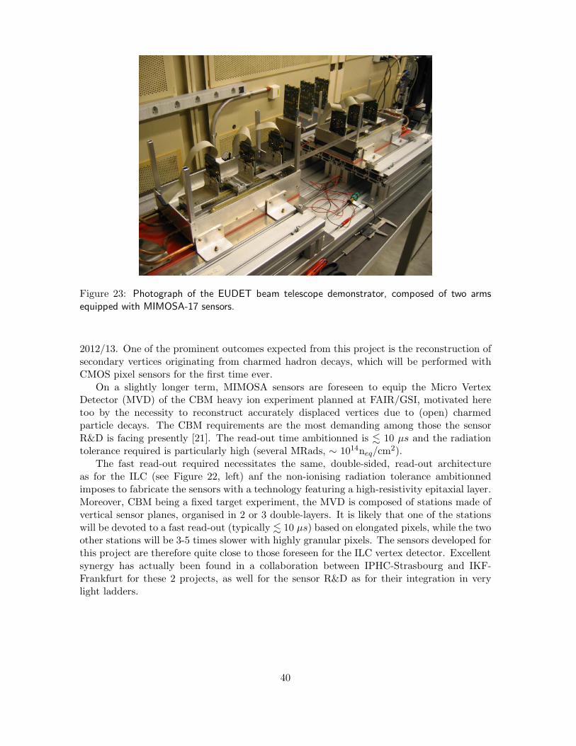
Figure 23: Photograph of the EUDET beam telescope demonstrator, composed of two armsequipped with MIMOSA-17 sensors.
2012/13. One of the prominent outcomes expected from this project is the reconstruction ofsecondary vertices originating from charmed hadron decays, which will be performed withCMOS pixel sensors for the first time ever.
On a slightly longer term, MIMOSA sensors are foreseen to equip the Micro VertexDetector (MVD) of the CBM heavy ion experiment planned at FAIR/GSI, motivated heretoo by the necessity to reconstruct accurately displaced vertices due to (open) charmedparticle decays. The CBM requirements are the most demanding among those the sensorR&D is facing presently [21]. The read-out time ambitionned is . 10 µs and the radiationtolerance required is particularly high (several MRads, ∼ 1014neq/cm
2).The fast read-out required necessitates the same, double-sided, read-out architecture
as for the ILC (see Figure 22, left) anf the non-ionising radiation tolerance ambitionnedimposes to fabricate the sensors with a technology featuring a high-resistivity epitaxial layer.Moreover, CBM being a fixed target experiment, the MVD is composed of stations made ofvertical sensor planes, organised in 2 or 3 double-layers. It is likely that one of the stationswill be devoted to a fast read-out (typically . 10 µs) based on elongated pixels, while the twoother stations will be 3-5 times slower with highly granular pixels. The sensors developed forthis project are therefore quite close to those foreseen for the ILC vertex detector. Excellentsynergy has actually been found in a collaboration between IPHC-Strasbourg and IKF-Frankfurt for these 2 projects, as well for the sensor R&D as for their integration in verylight ladders.
40
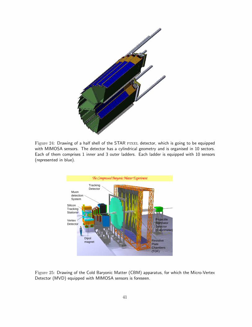
Figure 24: Drawing of a half shell of the STAR pixel detector, which is going to be equippedwith MIMOSA sensors. The detector has a cylindrical geometry and is organised in 10 sectors.Each of them comprises 1 inner and 3 outer ladders. Each ladder is equipped with 10 sensors(represented in blue).
Dipolmagnet
The Compressed Baryonic Matter Experiment
ResistivePlate Chambers(TOF)
SiliconTrackingStations
Tracking Detector
Muondetection System
Projectile SpectatorDetector(Calorimeter)
VertexDetector
Figure 25: Drawing of the Cold Baryonic Matter (CBM) apparatus, for which the Micro-VertexDetector (MVD) equipped with MIMOSA sensors is foreseen.
41
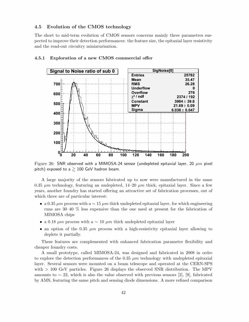
4.5 Evolution of the CMOS technology
The short to mid-term evolution of CMOS sensors concerns mainly three parametres sus-pected to improve their detection performances: the feature size, the epitaxial layer resistivityand the read-out circuitry miniaturisation.
4.5.1 Exploration of a new CMOS commercial offer
Figure 26: SNR observed with a MIMOSA-24 sensor (undepleted epitaxial layer, 20 µm pixelpitch) exposed to a & 100 GeV hadron beam.
A large majority of the sensors fabricated up to now were manufactured in the same0.35 µm technology, featuring an undepleted, 14–20 µm thick, epitaxial layer. Since a fewyears, another foundry has started offering an attractive set of fabrication processes, out ofwhich three are of particular interest:
• a 0.35 µm process with a ∼ 15 µm thick undepleted epitaxial layer, for which engineeringruns are 30–40 % less expensive than the one used at present for the fabrication ofMIMOSA chips
• a 0.18 µm process with a ∼ 10 µm thick undepleted epitaxial layer
• an option of the 0.35 µm process with a high-resistivity epitaxial layer allowing todeplete it partially.
These features are complemented with enhanced fabrication parametre flexibility andcheaper foundry costs.
A small prototype, called MIMOSA-24, was designed and fabricated in 2008 in ordreto explore the detection performances of the 0.35 µm technology with undepleted epitaxiallayer. Several sensors were mounted on a beam telescope and operated at the CERN-SPSwith > 100 GeV particles. Figure 26 displays the observed SNR distribution. The MPVamounts to ∼ 22, which is also the value observed with previous sensors [2], [9], fabricatedby AMS, featuring the same pitch and sensing diode dimensions. A more refined comparison
42
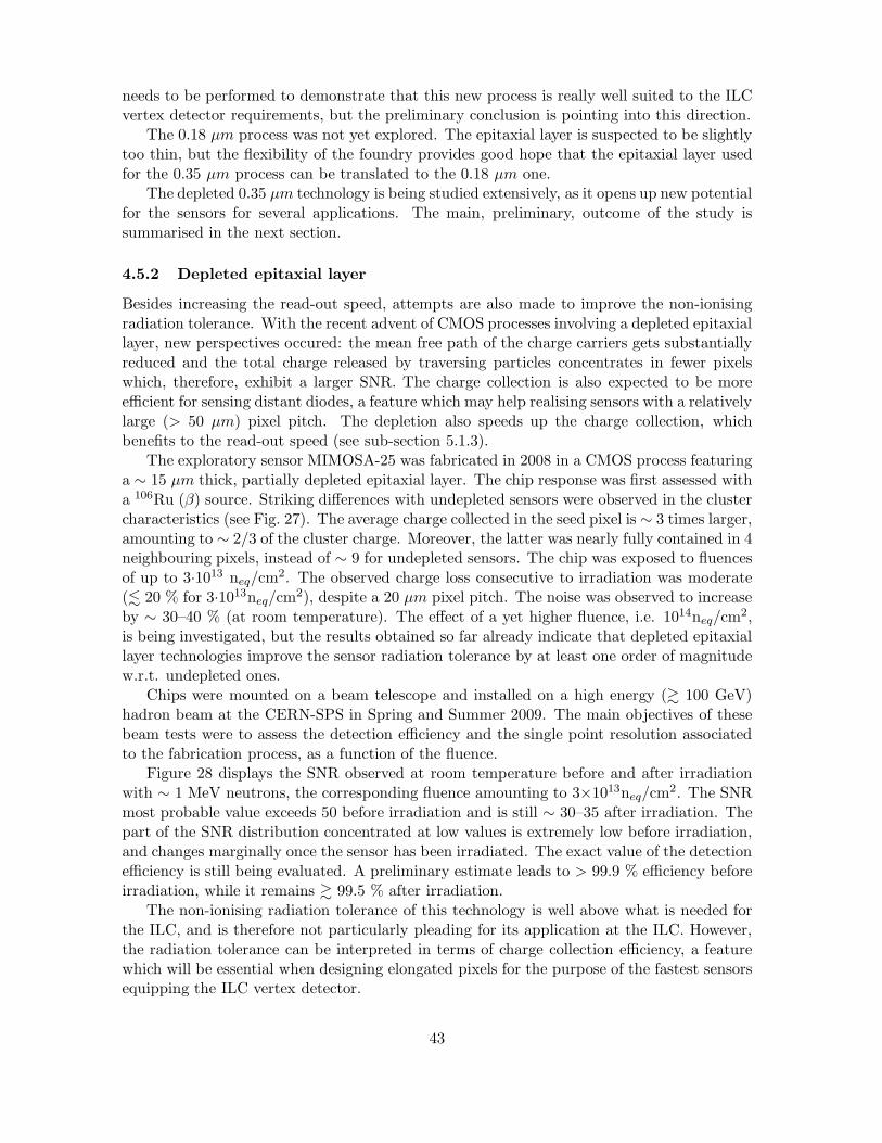
needs to be performed to demonstrate that this new process is really well suited to the ILCvertex detector requirements, but the preliminary conclusion is pointing into this direction.
The 0.18 µm process was not yet explored. The epitaxial layer is suspected to be slightlytoo thin, but the flexibility of the foundry provides good hope that the epitaxial layer usedfor the 0.35 µm process can be translated to the 0.18 µm one.
The depleted 0.35 µm technology is being studied extensively, as it opens up new potentialfor the sensors for several applications. The main, preliminary, outcome of the study issummarised in the next section.
4.5.2 Depleted epitaxial layer
Besides increasing the read-out speed, attempts are also made to improve the non-ionisingradiation tolerance. With the recent advent of CMOS processes involving a depleted epitaxiallayer, new perspectives occured: the mean free path of the charge carriers gets substantiallyreduced and the total charge released by traversing particles concentrates in fewer pixelswhich, therefore, exhibit a larger SNR. The charge collection is also expected to be moreefficient for sensing distant diodes, a feature which may help realising sensors with a relativelylarge (> 50 µm) pixel pitch. The depletion also speeds up the charge collection, whichbenefits to the read-out speed (see sub-section 5.1.3).
The exploratory sensor MIMOSA-25 was fabricated in 2008 in a CMOS process featuringa ∼ 15 µm thick, partially depleted epitaxial layer. The chip response was first assessed witha 106Ru (β) source. Striking differences with undepleted sensors were observed in the clustercharacteristics (see Fig. 27). The average charge collected in the seed pixel is ∼ 3 times larger,amounting to ∼ 2/3 of the cluster charge. Moreover, the latter was nearly fully contained in 4neighbouring pixels, instead of ∼ 9 for undepleted sensors. The chip was exposed to fluencesof up to 3·1013 neq/cm
2. The observed charge loss consecutive to irradiation was moderate(. 20 % for 3·1013neq/cm
2), despite a 20 µm pixel pitch. The noise was observed to increaseby ∼ 30–40 % (at room temperature). The effect of a yet higher fluence, i.e. 1014neq/cm
2,is being investigated, but the results obtained so far already indicate that depleted epitaxiallayer technologies improve the sensor radiation tolerance by at least one order of magnitudew.r.t. undepleted ones.
Chips were mounted on a beam telescope and installed on a high energy (& 100 GeV)hadron beam at the CERN-SPS in Spring and Summer 2009. The main objectives of thesebeam tests were to assess the detection efficiency and the single point resolution associatedto the fabrication process, as a function of the fluence.
Figure 28 displays the SNR observed at room temperature before and after irradiationwith ∼ 1 MeV neutrons, the corresponding fluence amounting to 3×10¹³neq/cm
2. The SNRmost probable value exceeds 50 before irradiation and is still ∼ 30–35 after irradiation. Thepart of the SNR distribution concentrated at low values is extremely low before irradiation,and changes marginally once the sensor has been irradiated. The exact value of the detectionefficiency is still being evaluated. A preliminary estimate leads to > 99.9 % efficiency beforeirradiation, while it remains & 99.5 % after irradiation.
The non-ionising radiation tolerance of this technology is well above what is needed forthe ILC, and is therefore not particularly pleading for its application at the ILC. However,the radiation tolerance can be interpreted in terms of charge collection efficiency, a featurewhich will be essential when designing elongated pixels for the purpose of the fastest sensorsequipping the ILC vertex detector.
43
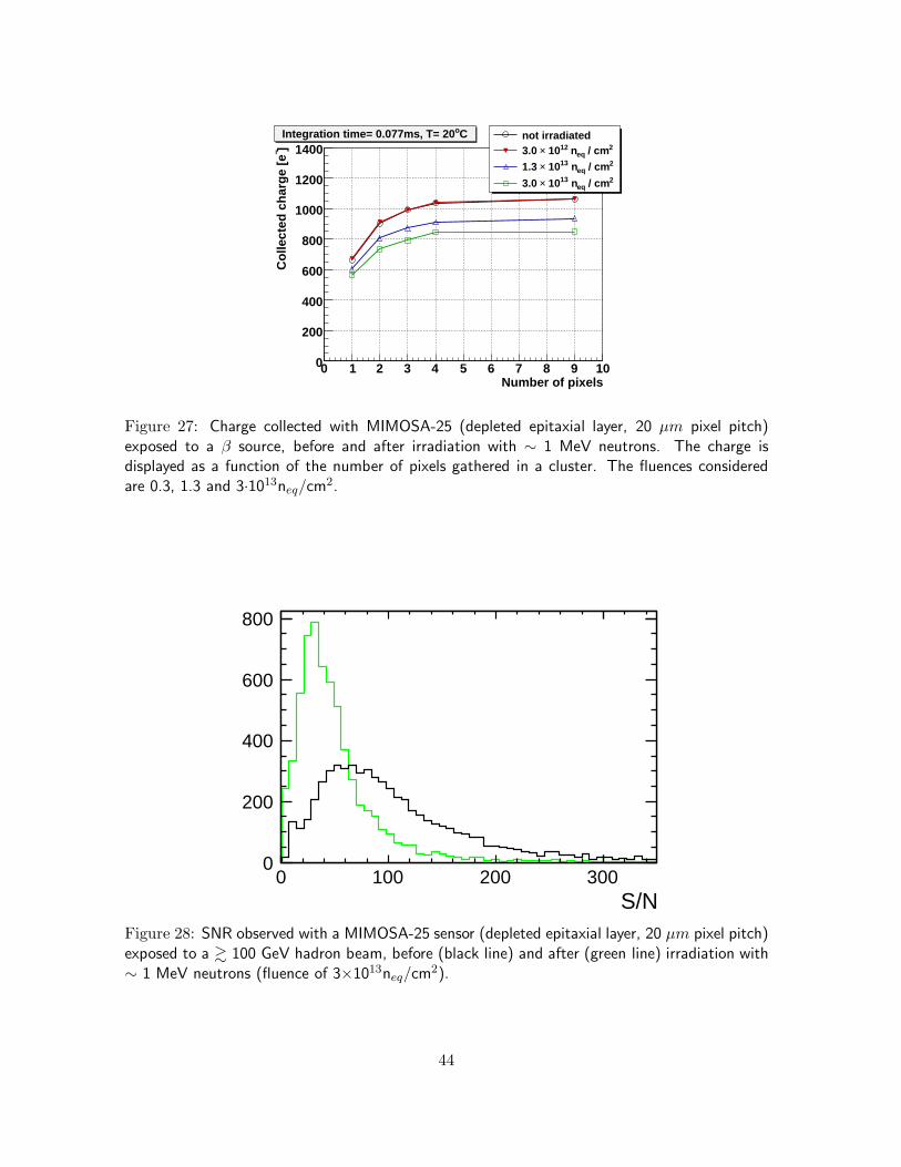
Number of pixels0 1 2 3 4 5 6 7 8 9 10
]−C
olle
cted
cha
rge
[e
0
200
400
600
800
1000
1200
1400not irradiated
2 / cmeq n12 10×3.0 2 / cmeq n13 10×1.3 2 / cmeq n13 10×3.0
CoIntegration time= 0.077ms, T= 20
Figure 27: Charge collected with MIMOSA-25 (depleted epitaxial layer, 20 µm pixel pitch)exposed to a β source, before and after irradiation with ∼ 1 MeV neutrons. The charge isdisplayed as a function of the number of pixels gathered in a cluster. The fluences consideredare 0.3, 1.3 and 3·1013neq/cm
2.
S/N0 100 200 300
0
200
400
600
800
Figure 28: SNR observed with a MIMOSA-25 sensor (depleted epitaxial layer, 20 µm pixel pitch)exposed to a & 100 GeV hadron beam, before (black line) and after (green line) irradiation with∼ 1 MeV neutrons (fluence of 3×10¹³neq/cm
2).
44
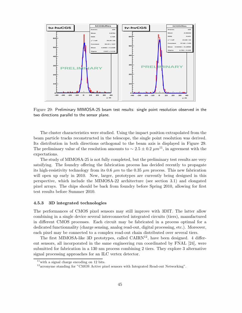
hCG5URes
Entries 425
Mean 0.8754
RMS 4.705
/ ndf 2χ 29.29 / 28
Constant 3.57± 55.22
Mean 0.1448± 0.8462
Sigma 0.116± 2.847
mµ
-40 -30 -20 -10 0 10 20 30 400
10
20
30
40
50
60
hCG5URes
Entries 425
Mean 0.8754
RMS 4.705
/ ndf 2χ 29.29 / 28
Constant 3.57± 55.22
Mean 0.1448± 0.8462
Sigma 0.116± 2.847
tu-huCG5
PRELIMINARY
hCG5VRes
Entries 425
Mean -0.06332
RMS 4.643
/ ndf 2χ 23.58 / 23
Constant 3.55± 57.22
Mean 0.14508± 0.04332
Sigma 0.103± 2.781
mµ
-40 -30 -20 -10 0 10 20 30 40
0
10
20
30
40
50
60
hCG5VRes
Entries 425
Mean -0.06332
RMS 4.643
/ ndf 2χ 23.58 / 23
Constant 3.55± 57.22
Mean 0.14508± 0.04332
Sigma 0.103± 2.781
tv-hvCG5
PRELIMINARY
Figure 29: Preliminary MIMOSA-25 beam test results: single point resolution observed in thetwo directions parallel to the sensor plane.
The cluster characteristics were studied. Using the impact position extrapolated from thebeam particle tracks reconstructed in the telescope, the single point resolution was derived.Its distribution in both directions orthogonal to the beam axis is displayed in Figure 29.The preliminary value of the resolution amounts to ∼ 2.5 ± 0.2 µm11, in agreement with theexpectations.
The study of MIMOSA-25 is not fully completed, but the preliminary test results are verysatsifying. The foundry offering the fabrication process has decided recently to propagateits high-resistivity technology from its 0.6 µm to the 0.35 µm process. This new fabricationwill open up early in 2010. New, larger, prototypes are currently being designed in thisperspective, which include the MIMOSA-22 architecture (see section 3.1) and elongatedpixel arrays. The chips should be back from foundry before Spring 2010, allowing for firsttest results before Summer 2010.
4.5.3 3D integrated technologies
The performances of CMOS pixel sensors may still improve with 3DIT. The latter allowcombining in a single device several interconnected integrated circuits (tiers), manufacturedin different CMOS processes. Each circuit may be fabricated in a process optimal for adedicated functionnality (charge sensing, analog read-out, digital processing, etc.). Moreover,each pixel may be connected to a complex read-out chain distributed over several tiers.
The first MIMOSA-like 3D prototypes, called CAIRN12, have been designed. 4 differ-ent sensors, all incorporated in the same engineering run coordinated by FNAL [24], weresubmitted for fabrication in a 130 nm process combining 2 tiers. They explore 3 alternativesignal processing approaches for an ILC vertex detector.
11with a signal charge encoding on 12 bits.12acronyme standing for ”CMOS Active pixel sensors with Integrated Read-out Networking”.
45
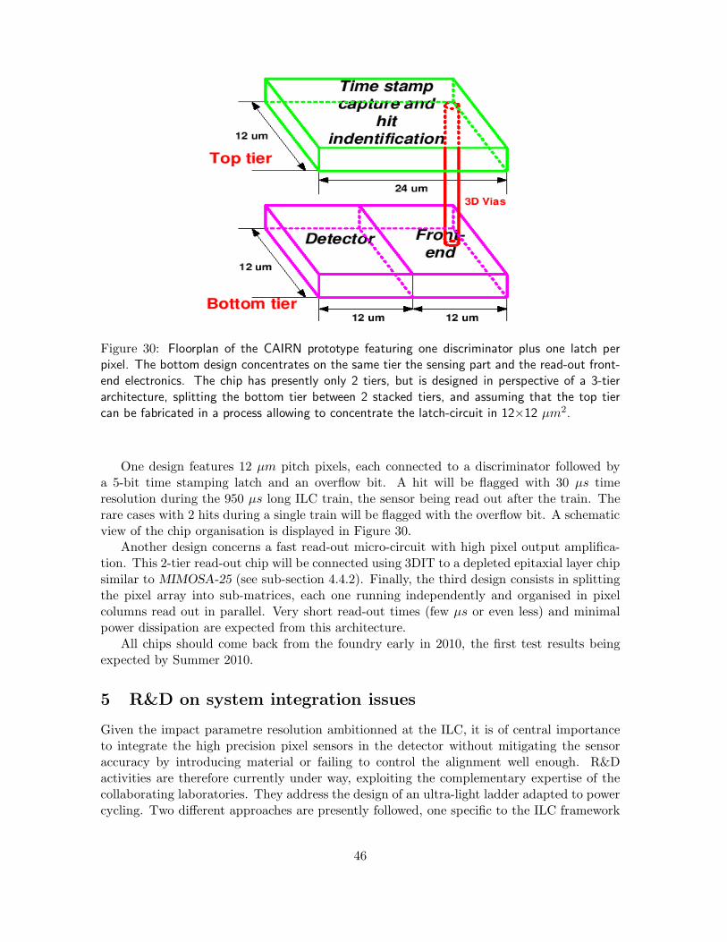
Figure 30: Floorplan of the CAIRN prototype featuring one discriminator plus one latch perpixel. The bottom design concentrates on the same tier the sensing part and the read-out front-end electronics. The chip has presently only 2 tiers, but is designed in perspective of a 3-tierarchitecture, splitting the bottom tier between 2 stacked tiers, and assuming that the top tiercan be fabricated in a process allowing to concentrate the latch-circuit in 12×12 µm2.
One design features 12 µm pitch pixels, each connected to a discriminator followed bya 5-bit time stamping latch and an overflow bit. A hit will be flagged with 30 µs timeresolution during the 950 µs long ILC train, the sensor being read out after the train. Therare cases with 2 hits during a single train will be flagged with the overflow bit. A schematicview of the chip organisation is displayed in Figure 30.
Another design concerns a fast read-out micro-circuit with high pixel output amplifica-tion. This 2-tier read-out chip will be connected using 3DIT to a depleted epitaxial layer chipsimilar to MIMOSA-25 (see sub-section 4.4.2). Finally, the third design consists in splittingthe pixel array into sub-matrices, each one running independently and organised in pixelcolumns read out in parallel. Very short read-out times (few µs or even less) and minimalpower dissipation are expected from this architecture.
All chips should come back from the foundry early in 2010, the first test results beingexpected by Summer 2010.
5 R&D on system integration issues
Given the impact parametre resolution ambitionned at the ILC, it is of central importanceto integrate the high precision pixel sensors in the detector without mitigating the sensoraccuracy by introducing material or failing to control the alignment well enough. R&Dactivities are therefore currently under way, exploiting the complementary expertise of thecollaborating laboratories. They address the design of an ultra-light ladder adapted to powercycling. Two different approaches are presently followed, one specific to the ILC framework
46

(called PLUME13), while the other is part of work package number 26 of the EU-FP7 projectcalled Hadron-Physics-2 [25].
5.1 PLUME project
The goal of the project is to prototype double-sided ladders equipped with pixel sensorsand assess their performances14. The project is supposed to provide, by 2012, the proofof principle of a ladder featuring . 0.3 % X0. It is thus not expected to match the mostambitious ILD vertex detector target values (e.g. 0.16 % X0), but it should end up close tothem and show the way towards their achievement. In particular, the geometry, stiffness,material budget and thermal properties of the ladder should be addressed quite extensively.
For those specifications which cannot be met, the performance achieved within the projectshould not depart from the target value by more than a factor of two. A value of 0.3 % X0
for the complete ladder material budget will therefore be satisfactory (the target value being0.16 % X0). An important aspect of the project is to assess the added value of double-sidedladders w.r.t. single-sided ones.
The ladder design is based on the ILD requirements for double-sided ladders equippingthe inner detector layer [3]. The most outstanding specification is the total material budget,but numerous other ones are also addressed in the project, as mentioned hereafter:
• active ladder width of 10 mm;
• active ladder length of 125 mm (assuming that butting two ladders will produce the250 mm length needed for the outer layers). The ladder has to support 6, ∼ 20 mmlong, sensors;
• inactive areas (for instance between two adjacent sensors) should not exceed a fractionin the ordre of 1-2 permill (i.e. ∼ 20-40 µm) of the geometrical acceptance;
• sensor thickness . 50 µm;
• one ended double-sided readout with only one cable outgoing from the ladder to theservicing board;
• compliance with passive cooling (individual sensors are expected to dissipate < 200 mW/cm2);
• compliance with power cycling in a 3-4 T magnetic field;
• mechanical stability preserving the sensor accuracy;
• relative initial mechanical positionning of the sensors on the ladder controled with aprecision allowing a high precision alignment.
A crucial hypothesis is that the CMOS sensors vertex detector at ILC will operate ina power cycling mode at room temperature, compatible with air flow cooling. Hence thesensors are assumed to be on top of all elements of a ladder.
For the final ladder, the compliance with all the requirements above is ambitionned,supported by experimental tests in the expected operational conditions, including power-cycling in a strong (3-4 T) magnetic field and air cooling. They should include beam teststo evaluate the pointing accuracy. The tests are also supposed to be complemented withmechanical stress simulations.
13acronyme standing for ”Pixelated Ladder using Ultra-light Material Embedding”.14present plans consist in integrating two different pixel technologies: MIMOSA sensors with continuous
read-out and ISIS sensors with delayed, slow, low power read-out.
47
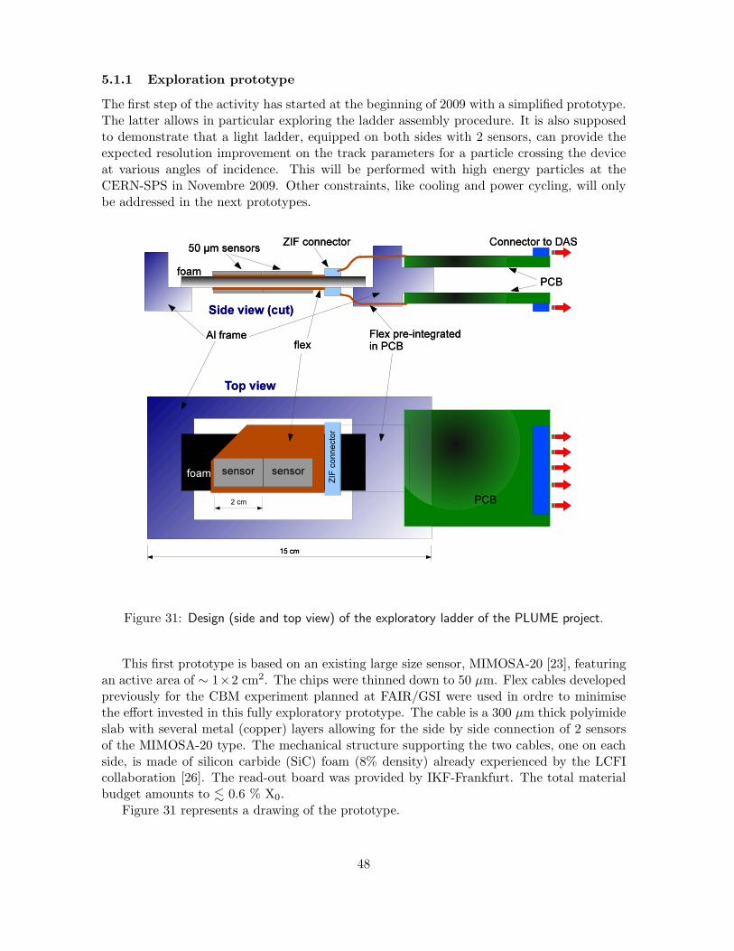
5.1.1 Exploration prototype
The first step of the activity has started at the beginning of 2009 with a simplified prototype.The latter allows in particular exploring the ladder assembly procedure. It is also supposedto demonstrate that a light ladder, equipped on both sides with 2 sensors, can provide theexpected resolution improvement on the track parameters for a particle crossing the deviceat various angles of incidence. This will be performed with high energy particles at theCERN-SPS in Novembre 2009. Other constraints, like cooling and power cycling, will onlybe addressed in the next prototypes.
Figure 31: Design (side and top view) of the exploratory ladder of the PLUME project.
This first prototype is based on an existing large size sensor, MIMOSA-20 [23], featuringan active area of ∼ 1×2 cm2. The chips were thinned down to 50 µm. Flex cables developedpreviously for the CBM experiment planned at FAIR/GSI were used in ordre to minimisethe effort invested in this fully exploratory prototype. The cable is a 300 µm thick polyimideslab with several metal (copper) layers allowing for the side by side connection of 2 sensorsof the MIMOSA-20 type. The mechanical structure supporting the two cables, one on eachside, is made of silicon carbide (SiC) foam (8% density) already experienced by the LCFIcollaboration [26]. The read-out board was provided by IKF-Frankfurt. The total materialbudget amounts to . 0.6 % X0.
Figure 31 represents a drawing of the prototype.
48
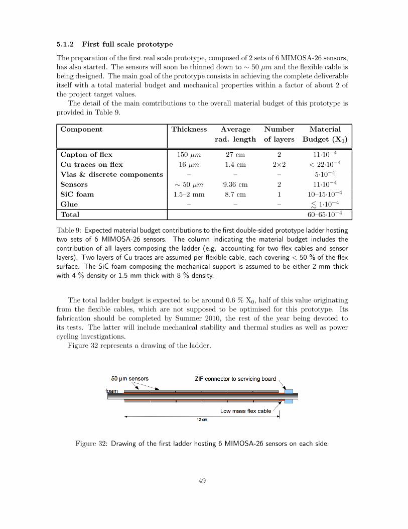
5.1.2 First full scale prototype
The preparation of the first real scale prototype, composed of 2 sets of 6 MIMOSA-26 sensors,has also started. The sensors will soon be thinned down to ∼ 50 µm and the flexible cable isbeing designed. The main goal of the prototype consists in achieving the complete deliverableitself with a total material budget and mechanical properties within a factor of about 2 ofthe project target values.
The detail of the main comtributions to the overall material budget of this prototype isprovided in Table 9.
Component Thickness Average Number Material
rad. length of layers Budget (X0)
Capton of flex 150 µm 27 cm 2 11·10−4
Cu traces on flex 16 µm 1.4 cm 2×2 < 22·10−4
Vias & discrete components – – – 5·10−4
Sensors ∼ 50 µm 9.36 cm 2 11·10−4
SiC foam 1.5–2 mm 8.7 cm 1 10–15·10−4
Glue – – – . 1·10−4
Total 60–65·10−4
Table 9: Expected material budget contributions to the first double-sided prototype ladder hostingtwo sets of 6 MIMOSA-26 sensors. The column indicating the material budget includes thecontribution of all layers composing the ladder (e.g. accounting for two flex cables and sensorlayers). Two layers of Cu traces are assumed per flexible cable, each covering < 50 % of the flexsurface. The SiC foam composing the mechanical support is assumed to be either 2 mm thickwith 4 % density or 1.5 mm thick with 8 % density.
The total ladder budget is expected to be around 0.6 % X0, half of this value originatingfrom the flexible cables, which are not supposed to be optimised for this prototype. Itsfabrication should be completed by Summer 2010, the rest of the year being devoted toits tests. The latter will include mechanical stability and thermal studies as well as powercycling investigations.
Figure 32 represents a drawing of the ladder.
Figure 32: Drawing of the first ladder hosting 6 MIMOSA-26 sensors on each side.
49
5.1.3 Next full scale prototypes
The next step of the project will focus on the total material budget. The number of traceson the flex cable will be minimised as well as its thickness, including the Cu trace thickness.The sensors may be thinned down to ∼ 35 µm, etc. The goal is to achieve a total materialbudget of ∼ 0.3–0.4 % X0. The ladder may be completed by Summer 2011 and its propertieswould then be evaluated through the rest of the year. It is only in 2012 that the productionof a ladder with . 0.3 % X0 may take place.
Depending on the success of the prototyping, it is envisaged to realise one ladder featuringsensors with two different pixel sizes on both of its faces. One sensor (mounted on the ladderside facing the beam pipe) would feature the squared pixels with the granularity necessaryfor the required high resolution on the impact parametre. The other sensor, equipping theladder side facing the external part of the detector, would feature elongated pixels alowingfor an integration time 4-6 times shorter than on the other side of the ladder.
Finally, it is worth mentioning that sets composed of overlapping ladder pairs are fore-seen to be used for alignment studies within an emerging EU-FP7 project, currently underpreparation and called AIDA15. In case this proposal gets approved by the EU, most ofthe system integration questions underlying the CMOS pixel sensor development could beinvestigated, including an extensive study of alignment issues.
5.2 Hadron Physics 2 project
Recent technical progress in industry has opened the perspective of mounting and connectingbutted sensors on a very thin flexible cable with the possibility to wrap the whole systemin a very thin polyimide film (see Figure 33). The complete device, called SERWIET16,is expected to stand for a total material budget of . 0.1 % X0, not accounting for themechanical support. It should be flexible and therefore potentialy adaptable to cylindricalsurfaces such as those of beam pipes. The most attactive perspective of the project is thusto realise a vertex detector layer which would use the beam pipe as a mechanical support,resulting in a substantial improvement of the impact parametre resolution for medium andlow momentum tracks.
The project is part of a work package composing the Hadron Physics 2 project, which issupported by the EU within FP-7, and was launched in January 2009. It is carried out inpartnership with the Nuclear Physics Research Institute of the Goethe University in Frank-furt, for the vertex detector of the CBM experiment planned at FAIR [21]. The conditionningof the sensors will be performed at IMEC [27], which is developping the technology. It willbe based on existing wafers of MIMOSA sensors.
The fabrication of the first prototype, composed of only one sensor (MIMOSA-18), willstart in Novembre 2009. The goal of the prototype is the following:
• commission a thinning procedure for the sensors resulting in a ∼ 25–35 µm thickness;
• commision a thin (25 µm thick) flexible cable fabrication;
• commission an accurate mounting procedure of the sensor on the cable;
• commission a connection procedure of the sensor to the cable;
15acronyme standing for ”Advanced Infrastructure for Detector Rat future Accelerators.”16standing for SEnsor Row Wrapped in Extra-Thin polyimide film
50

Figure 33: Hadron Physics 2 project deliverable. Schematic drawing of the prototype devicescomposed of thin sensors mounted on a thin flexible cable and wrapped in a thin polyimide film.The first prototype, incorporating only one sensor, is shown on the top. The bottom displayssome main features of the second prototype, composed of at least 3 sensors
• commission the wrapping of the system in a 25 µm thick polyimide film.
The device, which should be fabricated by Easter 2010, is represented schematically inFigure 33 (top). It will then be tested in Frankfurt and Strasbourg.
A second prototype, composed of & 3 sensors (see Figure 33 (bottom), will be manufac-tured once the tests of the first prototype are conclusive enough. While the sensor and theflex cable thickness should remain unchanged, a polyimide film of a thickness < 10 µm maybe used for part of the wrapping. The total material budget is therefore expected to endup below 0.1 % X0. The fabrication of this second prototype is expected to end in Summer2011. The rest of the year should then be used for its characterisation, which may includebeam tests and operation on the beam pipe of a running experiment.
5.3 Sensor butting
Ordinary chip fabrication results in individual sensors, which need to be butted on their flexcable and mechanical support once they have been diced. This approach presents advantagesbut has also drawbacks, mainly for what concerns the insensitive zones between neighbouringsensors and the difficulty to maintain a well controled alignment. On the other hand, it allowsselecting the sensors individually on the basis of their specific performances, once they havebeen characterised.
The possibility of fabricating sensors on reticles which are pushed closely together in onedirection, may allow producing sensors in ∼ 12 cm long slabs composed of 6 butted chips.This possibility is currently being investigated by one foundry which already fabricatedMIMOSA sensors in engineering runs. The hope is to reduce the insensitive zone betweensensors below 0.1-0.2 % of the total sensitive area.
The first trial, based on a . 20 µm wide sensor spacing, is expected to be launched beforethe end of 2009. This will provide a first estimate of the width of the insensitive band aswell as of the production yield.
51
6 Conclusions
The R&D of CMOS pixel sensors has gone through an important step in the last two years.A sensor design has been validated, which exhibits detection performances which are closeenough to the ILC vertex detector specifications that its (single step) extensions may suitthe requirements specific to the inner and outer layers. For the outer layers, which mayrequire integrating ADCs in the sensor, two ADC architectures have been prototyped atsmall scale, which may be suited to this purpose, provided their real scale validation will besuccessful. For the inner layers, a read-out time below 50 µs seems quite surely reachablewith a double-sided read-out of the chip.
Reducing the time resolution well below this value would clearly improve the physicsperformance of the detector. Attempts were initiated to achieve a 10 µs time stamping.The most promising mean in this direction exploits the possibility to equip one face of theinner double-layer with elongated pixels manufactured in a high resistivity technology (whichshould allow spacing the sensing diodes by > 50 µm without deteriorating significantly thecharge collection efficiency). This type of technology is currently under study, and hasalready provided excellent performances with a first, small scale, simple prototype (i.e. withno in-pixel signal processing circuitry).
The development of a very light double-sided ladder has also been undertaken, basedon the complementary expertise of several laboratories belonging to the ILC community.This project, called PLUME, is complemented with the study of a wrapping technologyexpected to allow for a material budget amounting to < 0.1 % X0 for a system composedof the sensors, a flexible cable, connections, fixtures and the film used for embedding. Thepossibility will be explored of mounting such a device on a cylindrical surface, possibly abeam pipe, exploiting its flexibility. Other studies, such as sensor butting with marginaldead zones, are also under way. The advent of the EU project AIDA, which focusses onintegration issues (e.g. alignment, mechanicial stability), would complement these activitiesquite perfectly.
Finally, the R&D of a new generation of CMOS sensors has started in 2009, which relieson vertical integration technologies. Its main advantages are to allow combining differentCMOS processes in a single chip and to squeeze the time resolution to a few microseconds,or perhaps even less. Several alternative sensor designs have been submitted for fabricationin a 130 nm technology inteconnecting a stack of two tiers. The architectures developedinclude delayed and continuous read-out alternatives, as well as low power consumption, fastread-out, designs. A first idea of the outreach of 3DIT CMOS sensors is expected by Summer2010.
The next important step of the preparation of experiments for the ILC is the TechnicalDesign Report relying on a Detailed Baseline Design (DBD), to be delivered by the end of2012. By this date, the sensor designs specific to the inner and outer layers of the vertexdetector are expected to be fabricated and characterised at real scale, including the optionof elongated pixels.
It is also likely that the double-sided ladder concept, and its added value w.r.t. thesingle-sided one, will be quite well understood. The potential of the polyimide film wrappingapproach should also be known. Moreover, several system integration issues (e.g. alignment,power cycling), should have been addressed, in particular if the AIDA proposal to the EUgets approved.
One may thus expect that the 2-3 coming years will allow evaluating in how far the
52

specifications of a vertex detector concept based on the most advanced existing technologiesof the moment, are reachable.
53
APPENDIX: List of Chips mentioned in the Report
MIMOSA-5 first reticle size sensor (analog read-out)
1024×1024 pixels with 17 µm pitch
MIMOSA-6 first sensor with integrated signal processing micro-circuits
column parallel read-out with 28 µm pitch
MIMOSA-8 improved version of MIMOSA-6, fabricated in TSMC-0.25 technology
32 columns of 128 pixels, with 25 µm pitch
MIMOSA-9 analog output sensor used to assess the AMS-0.35 technology
several different pixel matrices with 20–40 µm pitch
MIMOSA-14 developed for the STAR-pixel prototyping
128×128 pixels with 30 µm pitch
MIMOSA-16 translation of MIMOSA-8 in AMS-0.35 technology
32 columns of 128 pixels with 25 µm pitch
MIMOSA-17 equips both arms of EUDET beam telescope demonstrator
256×256 pixels with 30 µm pitch
MIMOSA-18 equips DUT of EUDET beam telescope demonstrator
512×512 pixels with 10 µm pitch (. 1 µm resolution)
MIMOSA-20 enlarged version of MIMOSA-14 for the STAR pixel prototyping
640×320 pixels (1×2 cm2 active area) with 30 µm pitch
MIMOSA-22 enlarged version of MIMOSA-16 (integrated CDS and discriminators) with smaller pitch
128 columns of 576 pixels with 18.4 µm pitch read out in ∼ 90 µs
SUZE-01 zero-suppression prototype micro-circuit with output memories
adapted to a pair of 64 columns
MIMOSA-23 enlarged version of MIMOSA-22 for the STAR pixel demonstrator
640 columns of 640 pixels with 30 µm pitch (2×2 cm2 active area) read out in 640 µs
MIMOSA-24 first (small) prototype exploring a new 0.35 µm technology
MIMOSA-25 first (small) prototype exploring a high-resistivity epitaxial layer (0.6 µm ) technology
MIMOSA-26 final EUDET beam telescope sensor, with integrated zero-suppression
1152 columns of 576 pixels with 18.4 µm pitch (1×2 cm2 active area) read out in ∼ 110 µs
MIMOSA-28 extension of MIMOSA-26 being designed for the STAR pixel detector
1088 columns of 103 pixels with 18.4 µm pitch (20×18.5 mm2 active area) read out in . 200 µs
Table 10: List of chips mentioned in the report. Most of them were fabricated in the 0.35µm opto process of AMS. The exceptions are MIMOSA-6 (AMI-0.35 µm process), MIMOSA-8(TSMC-0.25 µm process), MIMOSA-24 (XFAB-0.35 µm process) and MIMOSA-25 (XFAB-0.6µm process). MIMOSA-28 is also foreseen to be manufactured in the AMS 0.35 µm technology.
54
References
[1] Turchetta et al., A Monolithic Active Pixel Sensor for charged particle tracking and imagingusing standard VLSI CMOS technology, Nuclear Instruments & Methods in Physics ResearchSection A 458 (2001) 677-689;
[2] M.Winter et al., A swift and slim flavour tagger exploiting the CMOS sensor technology, pro-ceedings of the Linear Collider Workshop LCWS-05, Stanford, USA, March 2005;
[3] ILD concept group, Letter of Intent of the Internationlal Large Detector (ILD),http://www.ilcild.org/documents/ild-letter-of-intent/LOI.pdf, March 2009;
[4] R. De Masi et al., Estimate of the background in the ILD vertex detector due to beamstrahlung,http://www.ilcild.org/documents/ild-loi-material/BKGStudies.pdf/at download/file, LC-Notein preparation.
[5] G.Deptuch et al., Monolithic Active Pixel Sensors with In-Pixel Double Sampling Operation andColumn-Level Discrimination, IEEE Trans. Nucl. Sci. 51 (2004), 2313-2321, Proc. of the IEEENuclear Science Symposium, Portland (Oregon), September 2003;
[6] Y. Degerli et al., A Fast Monolithic Active Pixel Sensor With Pixel-Level Reset Noise Suppressionand Binary Outputs for Charged Particle Detection, IEEE Trans. Nucl. Sci. 52 (2005), 3186, Proc.of the IEEE Nuclear Science Symposium, Roma (Italy), Octobre 2004;
[7] Y.Degerli et al., Development of Binary Readout CMOS Monolithic Sensors for MIP Tracking,IEEE Trans. Nucl. Sci. 56 (2009) 354;
[8] M.Winter et al., PRC report of May 2005
[9] M.Winter et al., PRC report of May 2007
[10] EUDET collaboration, ”Detector R&D towards the International Linear Collider”, supportedby the E.U. within FP6, http://www.eudet.org/;T. Haas, A pixel telescope for detector R&D for an International Linear Collider, Nucl. Inst.Meth. A 569 (2006) 53-56;
[11] G. Claus et al., IDC, alias MIMOSA-22, status report EUDET-Memo-2008-03;
[12] Austriamicrosystems AG, Tobelbaderstrasse 30, Schloss Premstaetten A 8141 Unterpremstaet-ten;
[13] IEEE 1149.1 Rev1999;
[14] MIMOSA-22 User Manual;
[15] A. Dorokhov, NMOS-based high gain amplifier for MAPS, International meeting on front endelectronics for high energy, nuclear and space applications, Perugia, Italy, 17- 20 May 2006;
[16] A. Dorokhov, Optimization of amplifiers for Monolithic Active Pixel Sensors. TWEPP-07, Top-ical Workshop on Electronics for Particle Physics, Prague, Czech Republic, 3–7 Sept. 2007;
[17] M.Deveaux et al., Charge collection properties of X-ray irradiated monolithic active pixel sensors,Nucl. Inst. & Meth. A, Vol. 552 (2005), 118-123;
[18] A. Himmi et al., SDC-2, alias SUZE, zero suppression micro-circuit status report, EUDET-Memo-2007-55;
[19] M.Dahoumane, PhD thesis, defended on November 3rd, 2009, unpublished;
[20] N.Pillet et al., A Pixel Level, Ultra Low Power, 10Msample/s Double Ramp A/D Converter forMonolithic Active Pixel Sensors in High Energy Physics and Biomedical Imaging Applications,Proc. of 12th conference on design of circuits and integrated systems, Sevilla (Spain), 21-23Novembre 2007;
[21] J.Heuser et al. (for the CBM collaboration), The Compressed Baryonic Matter experiment atFAIR: physics of strangeness and charm, status of preparations, J. Phys. G: Nucl. Part. Phys.35 (2008);M.Winter et al., Achievements of CMOS Pixel Sensors for the CBM Micro-Vertex Detector, GSIScientific Report 2007.
55

[22] see [9]
[23] M. Szelezniak et al., Small-Scale Readout System Prototype for the STAR pixel Detector, IEEETrans. Nucl. Sci. 55 (2008) 3665
[24] R.Yarema, The First Vertically Integrated MPW Run for HEP, contribution to the TWEPP-09workshop, Paris, 21-25 Septembre 2009.
[25] FP-7 Integrated Activity project addressing the Study of strongly interacting matter,www.hadronphysics2.eu/
[26] http://hepwww.rl.ac.uk/LCFI/
[27] IMEC is Europe’s largest independent research center in nano-electronics and nano-technology.www.imec.be/
56


![Using a high spatial resolution tactile sensor for intention detection · 2016-04-28 · tactile sensor system [6] with a spatial resolution of 5mm and a wide dynamic range, which](https://static.fdocuments.us/doc/165x107/5eda77c1b3745412b5716456/using-a-high-spatial-resolution-tactile-sensor-for-intention-detection-2016-04-28.jpg)