
DEVELOPMENT OF STABLE METAL OXIDE …xr045qb7231/Jonathan Prange... · DEVELOPMENT OF STABLE METAL...
174
DEVELOPMENT OF STABLE METAL OXIDE ELECTRODES FOR THE CONVERSION OF ELECTRICITY TO CHEMICAL FUELS A DISSERTATION SUBMITTED TO THE DEPARTMENT OF CHEMISTRY AND THE COMMITTEE ON GRADUATE STUDIES OF STANFORD UNIVERSITY IN PARTIAL FULFILLMENT OF THE REQUIREMENTS FOR THE DEGREE OF DOCTOR OF PHILOSOPHY Jonathan David Prange July 2011
Transcript of DEVELOPMENT OF STABLE METAL OXIDE …xr045qb7231/Jonathan Prange... · DEVELOPMENT OF STABLE METAL...

DEVELOPMENT OF STABLE METAL OXIDE ELECTRODES FOR THE
CONVERSION OF ELECTRICITY TO CHEMICAL FUELS
A DISSERTATION SUBMITTED TO THE DEPARTMENT OF CHEMISTRY AND
THE COMMITTEE ON GRADUATE STUDIES OF STANFORD UNIVERSITY IN
PARTIAL FULFILLMENT OF THE REQUIREMENTS FOR THE DEGREE OF
DOCTOR OF PHILOSOPHY
Jonathan David Prange
July 2011

http://creativecommons.org/licenses/by-nc/3.0/us/
This dissertation is online at: http://purl.stanford.edu/xr045qb7231
© 2011 by Jonathan David Prange. All Rights Reserved.
Re-distributed by Stanford University under license with the author.
This work is licensed under a Creative Commons Attribution-Noncommercial 3.0 United States License.
ii

I certify that I have read this dissertation and that, in my opinion, it is fully adequatein scope and quality as a dissertation for the degree of Doctor of Philosophy.
Christopher Chidsey, Primary Adviser
I certify that I have read this dissertation and that, in my opinion, it is fully adequatein scope and quality as a dissertation for the degree of Doctor of Philosophy.
T Stack
I certify that I have read this dissertation and that, in my opinion, it is fully adequatein scope and quality as a dissertation for the degree of Doctor of Philosophy.
Robert Waymouth
Approved for the Stanford University Committee on Graduate Studies.
Patricia J. Gumport, Vice Provost Graduate Education
This signature page was generated electronically upon submission of this dissertation in electronic format. An original signed hard copy of the signature page is on file inUniversity Archives.
iii

iv
Abstract
The conversion of renewable sources of electricity to molecular fuels is widely
viewed as an important component of our future energy economy. To accomplish this,
stable electrodes are necessary to perform electrochemical reactions of interest for
extended periods of operation with high efficiency. In the first part of this thesis, a
method to immobilize homogeneous catalysts to a metal oxide electrode through click
chemistry on an attached p-azidophenyl phosphonic acid linker is presented. This
strategy allows for a convergent approach to surface modification that results in stable
attachments while allowing for facile charge transfer between the electrode and the
immobilized catalyst. The deposition of p-azidophenyl phosphonic acid to the metal
oxide surface and subsequent click with molecules of interest was investigated with
Fourier transform infrared spectroscopy, electrochemistry and X-ray photoelectron
spectroscopy.
The electrochemical oxidation of water to supply the electrons needed for fuel synthesis
remains a challenge due to the lack of materials which can both efficiently remove four
electrons and withstand the harsh oxidative conditions of the reaction. A novel type of
dimensionally stable anode utilizing silicon as the base substrate and also as an in-situ
photon collector has been developed. It uses a thin layer of titanium dioxide deposited
by atomic layer deposition to protect the silicon. A thin layer of physical vapor
deposited iridium is used as the water oxidation catalyst. Results shown include water
oxidation efficiency in both light and dark conditions and over a range of pH values
with an emphasis on the operational stability and durability of the anodes.

v
Acknowledgements
I would like to first start by thanking my thesis advisor, Professor Christopher E.
D. Chidsey, for all of his training, insight and guidance, and ultimately giving me the
opportunity to prove myself in his laboratory. His suggestions, comments and advice
have shaped the way I approach problems and obstacles, not only in science, but in
every aspect of my life. I would also like to thank my committee chair, Professor Paul
C. McIntyre, whom I consider more of a co-advisor and collaborator. Working with
Professor McIntyre has been a tremendous experience and I truly appreciate all of his
guidance and support as well as his suggestions and insights into our work. I am also
very grateful for my two readers and collaborators, Professor T. Daniel P. Stack and
Professor Robert M. Waymouth. Professor Stack and Professor Waymouth helped me
navigate my graduate career by offering advice and suggestions on anything from my
research project and proposals to the difficult situation of switching research groups in
the middle of my graduate career. I would also like to thank Professor Justin DuBois,
my non-reader, and Professor Richard Zare for their support and helping me through the
transition of switching labs.
I would also like to thank my first research advisor, Professor Dmitry Yandulov.
Professor Yandulov taught me a lot about inorganic reaction mechanisms and kinetics
as well as helping me master some advanced laboratory techniques.
I thank Professor Thomas Jaramillo and Professor Matthew Kanan for the many
fruitful discussions about science and energy. Their suggestions and insights have been

vi
greatly appreciated and I have learned so much from both of them. I look forward to
their contributions to this field in the future. I thank Dr. Todd A. Eberspacher whom is
a great resource in so many ways. His no nonsense approach to problem solving has
made my graduate career that much easier. He is also one of the most knowledgeable
people I have met at Stanford. Dr. Steve Lynch has also been a tremendous resource for
both the optics facility and the NMR facility. Chuck Hitzman has also been great in
helping out with using the XPS and all the software questions I have had.
I am truly grateful for all my collaborators throughout my graduate career.
Randall Lowe first made the p-azidophenyl phosphonic acid and selflessly allowed me
to work with it. I am very grateful for this and the scientific knowledge he has given
me over the years. He is one of the most capable people I have met and I thank him for
his friendship and all his fruitful discussions. I am also thankful for Alissa Sasayama,
who helped tremendously on this project. From the McIntyre Lab, I would like to thank
Yi Wei (Vincent) Chen. Vincent has worked on the solar water splitting project with
me for a major portion of my graduate career. He is one of the smartest, hardest
working and selfless people I have met at Stanford. He is also persistent, as he has
attempted over and over again to teach me solid state physics to no avail. Without him,
this project doesn’t go anywhere, and I am so thankful for his scientific and personal
friendship, he truly is a great scientist and great person. Simon Duehnen has also been a
great pleasure to work with. He worked very hard on the water splitting project and
became a completely independent scientist by the end of his stay at Stanford. I look
forward to visiting him in Germany soon. Ali Hosseini deserves a mention here, as he

vii
has always been helpful with any question I have ever had on any project, he is a great
friend.
I also want to thank all of the current and former Chidsey group members for all
their help and ultimately putting up with me in the office and lab. In no particular
order, Randall Lowe, Ali Hosseini, Simon Duehnen, Charles McCrory, Anando
Devadoss, Josh Ratchford, Alex Neuhausen, Vadim Ziatdinov and the undergrads
Alissa Sasayama, Marty Casey, Jeff Jensen and David Lapham. I want to thank
members of the McIntrye lab as well, for putting up with me and all my requests for
ALD samples. In no particular order: Vincent Chen, Marika Gunji, Jaesoon Ahn,
Rathnait Long, Shu Hu, Rahim Esfandyarpour, Cynthia Ginestra and Andy Lin. I
would also like to mention my former lab mates in the Yandulov lab: Eunsung Lee,
Kendra Kuhl, Jessica DeMott, Sang-won Kwo, Ngon Tran and Georg Platz.
I have had a great relationship with members of both Professor Stack’s group
and Professor Waymouth’s group. I want to thank everyone I have interacted with in
these two labs over the years, but would like to mention, in no particular order, Pratik
Verma, Matt Pellow, Brian Smith, Eric Stenjehem, and Tim Storr from the Stack Lab
and Matt and Liz Kiesewetter, David Pearson, Kristen Brownell and Antoni DeCrisi
from the Waymouth Lab. Thank you again to both of these labs for everything from
letting me ‘borrow’ lab equipment to suggestions and random conversations. I would
also like to thank all those involved in the GCEP collaboration from the labs of
Professor Chidsey, Stack, Waymouth and Jaramillo. There are many graduate students
and post docs that have contributed to my positive experience in graduate school, not to
name them all, but I do thank all of you.

viii
I am also grateful for Roger Kuhn, Patricia Dwyer and everyone else in the
Chemistry department front office. They work so hard and are the best at what they do.
I will miss having them around to make my life easier.
I would also especially thank my close friends here: Kevin and Cara, Brian and
Moria, Colin and Andi, Jason Wagnor and Scott Tabakman. You guys are the best. I
couldn’t have done this without you guys.
My graduate career was full of ups and downs. The one consistency was always
my family. My dad and mom, Dave and Carol Prange, have prepared me my whole life
to meet all the challenges I have ever been presented here in graduate school and in life,
and I am so grateful for them. I would also like to mention all of my brothers and
sisters and their spouses: Malinda and Tim Smith, Scott and Laurie Prange, Vanessa
and Matthew Ewing, and Chris Prange and his girlfriend, Shawna. They have been
very supportive and a great source of encouragement and happiness throughout my time
here. I would also like to thank the best nieces and nephews an uncle could have:
Courtney and Josh, and Asheley and Tyler (and any future ones). You guys are
awesome and I enjoy spending time with all of you, and I am sorry I haven’t been
around much these last few years. Finally, I want to thank my best friend, Sarah
Sherlock. She is the best thing to happen to me at Stanford, and without her
unconditional love and unwavering strength and support, this would not have been
possible. I love her and appreciate her more than she will ever know. This thesis is for
all of you, thank you for everything.

ix
Table of Contents
Abstract .......................................................................................................................... iv
Acknowledgements ......................................................................................................... v
Table of Contents ........................................................................................................... ix
List of Figures .............................................................................................................. xiii
Chapter 1: Introduction ................................................................................................ 1
1.1: Thesis Objective ............................................................................................... 1
1.2: Background ........................................................................................................ 2
Modification of Metal Oxide Electrodes .................................................. 2
Protecting Photoanodes Used in Solar Water Splitting ............................ 5
1.3: Analytical Methods ............................................................................................ 7
Fourier Transform Infrared Spectroscopy ................................................ 7
X-Ray Photoelectron Spectroscopy .......................................................... 7
Electrochemical Methods ......................................................................... 8
1.4: Methodology ................................................................................................... 11
1.5: Collaborations ................................................................................................. 12
1.6: Figures ............................................................................................................ 13
1.7: References ....................................................................................................... 18

x
Chapter 2: Modification of Indium Tin Oxide Electrodes with p-Azidophenyl
Phosphonic Acid ........................................................................................................... 20
2.1: Preface ............................................................................................................ 20
2.2: Abstract ........................................................................................................... 21
2.3: Introduction ..................................................................................................... 22
2.4: Materials and Methods .................................................................................... 25
2.5: Results and Discussion ................................................................................... 30
2.6: Conclusion ...................................................................................................... 37
2.7: Figures ............................................................................................................. 38
2.8: References and Notes ...................................................................................... 47
2.9: Supporting Information ................................................................................... 52
Chapter 3: Introduction ............................................................................................... 64
3.1: Abstract ........................................................................................................... 64
3.2: The Global Energy Challenge ......................................................................... 65
Renewable and Alternative Sources of Energy ...................................... 67
3.3: Solar Water Splitting ...................................................................................... 69
Photoanodes and Water Oxidation Catalysts ......................................... 74
Protection of Photoanodes Used in Solar Water Splitting ...................... 76
3.4: Figures ............................................................................................................ 79
3.5: References ....................................................................................................... 84

xi
Chapter 4: Stable Si Photoanodes for Water Splitting ............................................ 90
4.1: Preface ............................................................................................................ 90
4.2: Abstract ........................................................................................................... 91
4.3: Introduction ..................................................................................................... 92
4.4: Results and Discussion ................................................................................... 95
4.5: Conclusion .................................................................................................... 101
4.6: Methodology ................................................................................................. 102
4.7: Figures .......................................................................................................... 104
4.8: References ..................................................................................................... 112
4.9: Supporting Materials ..................................................................................... 117
4.10: Supporting Materials Figures ...................................................................... 123
Chapter 5: Effect of TiO2 Thickness and Catalyst Layer on Efficiency and
Stability of Silicon Anodes for Water Oxidation ..................................................... 134
5.1: Preface .......................................................................................................... 134
5.2: Abstract ......................................................................................................... 135
5.3: Introduction ................................................................................................... 136
5.4: Results and Discussion ................................................................................. 137
5.5: Conclusions ................................................................................................... 143
5.6: Figures .......................................................................................................... 144
5.7: References ..................................................................................................... 148

xii
5.8: Supporting Materials ..................................................................................... 151
5.9: Supporting Materials Figures ........................................................................ 156
5.10: Supporting Materials References ................................................................ 160

xiii
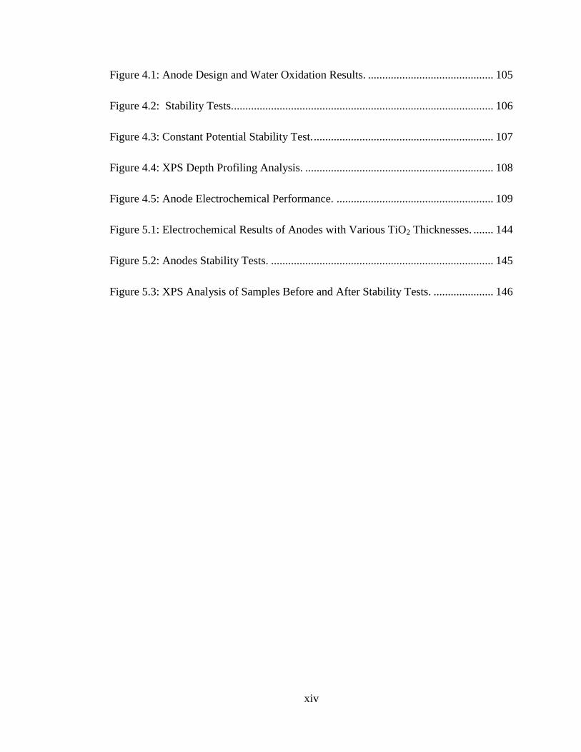
List of Figures
Figure 1.1: Illustration of immobilization strategy ......................................................... 13
Figure 1.2: Titanium Pourbaix Diagram. ...................................................................... 14
Figure 1.3: Electrochemical Water Oxidation Setup. .................................................... 15
Figure 1.4: FTIR Total Reflectance Accessory. ............................................................. 16
Figure 1.5: ALD Process. ............................................................................................... 17
Figure 2.1: Immobilization Schematic. ......................................................................... 38
Figure 2.2: XPS Analysis. .............................................................................................. 39
Figure 2.3: Deposition of p-Azidophenyl Phosphonic Acid. ......................................... 40
Figure 2.4: FTIR Spectrum Before and After Click. ...................................................... 41
Figure 2.5: Cyclic Voltammogram of Clicked Ethynylferrocene. ................................. 42
Figure 2.6: Click Results for Azide-terminated Monolayers. ........................................ 43
Figure 2.7: Mixed Monolayers on ITO. ......................................................................... 44
Figure 2.8: Effect of Water on p-Azidophenyl Phosphonic Acid Deposition. ............... 45
Figure 2.9: Stability of Azide on ITO Surface. .............................................................. 46
Figure 3.1: Current and Future Global Energy Demand. ............................................... 79
Figure 3.2: Solar Spectrum. ............................................................................................ 80
Figure 3.3: Band Gaps of Common Semiconductors. .................................................... 81
Figure 3.4: Recombination Pathways for Photogenerated Electron/Hole Pairs. ............ 82
Figure 3.5: Photoelectrochemical Water Splitting Configurations. ............................... 83
xiv
Figure 4.1: Anode Design and Water Oxidation Results. ............................................ 105
Figure 4.2: Stability Tests. ........................................................................................... 106
Figure 4.3: Constant Potential Stability Test. ............................................................... 107
Figure 4.4: XPS Depth Profiling Analysis. .................................................................. 108
Figure 4.5: Anode Electrochemical Performance. ....................................................... 109
Figure 5.1: Electrochemical Results of Anodes with Various TiO2 Thicknesses. ....... 144
Figure 5.2: Anodes Stability Tests. .............................................................................. 145
Figure 5.3: XPS Analysis of Samples Before and After Stability Tests. ..................... 146
1
Chapter 1: Introduction
1.1: Thesis Objective
The specific topics of my thesis are: (a) understanding the attachment and
coverage of p-azidophenyl phosphonic acids on conductive metal oxide electrodes and
(b) developing oxide tunnel barriers to protect low band gap semiconductors employed
for photoelectrochemical oxidation of water. These two topics are related by the overall
objective of understanding how to transfer electrons between a species in solution and
an electrode in order to interconvert electricity and chemical fuels. A fundamental
understanding and control of electron transfer reactions to and from effective catalysts
on corrosion resistant electrode surfaces will enable the construction of more efficient
and robust electrochemical devices important for small molecule oxidation or reduction
necessary for renewable electricity production and storage.

2
1.2: Background
Modification of Metal Oxide Electrodes
The first project in this thesis is an investigation into the modification of a metal
oxide (MO) electrode with compounds of interest from solution. The use of MO
electrodes for applications such as fuel cells and organic photovoltaic devices often
requires modification of the surface to achieve the desired properties. For example,
many reactions of interest in a fuel cell, such as the four electron reduction of dioxygen
to water, are found to be sluggish or inefficient at the MO electrode surface. The ability
to modify the MO surface with an active catalyst for this reaction would be highly
desirable. This strategy also holds true for organic photovoltaic devices, where a light
absorbing organic compound must be attached to a transparent conductive MO
electrode in order to efficiently inject the photogenerated charge into the device. In
these applications, a well-defined and robust attachment of various compounds of
interest, either catalysts or light absorbing molecules, is required for operation.
A variety of attachment functionalities, or anchors, to a MO surface are known
including siloxanes, carboxylic acids and phosphonic acids.1-4
These molecules are all
claimed to form self-assembled monolayers (SAMs) on MO surfaces from a deposition
solution containing the adsorbate and the MO electrode. Each one of these anchors
could potentially form multiple bonds to the surface resulting in a chemically and
thermally stable attachment. Although these functional groups attach to the surface
readily from solution, some challenges must be overcome before implementation in an
operational device. First, charges must be able to transfer between the MO surface and

3
catalyst or light absorbing molecule that is attached to it. Second, synthesizing one of
these attachment functional groups to every catalyst or small molecule of interest
presents a formidable challenge. A method to immobilize a compound and retain its
function on a surface while not having to go through elaborate synthetic procedures
would be highly desirable.
The strategy employed in Chapter Two of this thesis is to synthesize a p-
azidophenyl phosphonic acid that could act as an anchor to the surface and a linker to a
molecule of interest in solution. The phosphonic acid group of this molecule will act as
the anchoring group to a MO surface, attaching in a bi-dentate or tri-dentate mode.5
The azide group of the p-azidophenyl phosphonic acid will allow for the coupling of
various ethynyl-terminated molecules in solution. The pi system of the entire molecule
will allow for facile electron transfer between the MO electrode surface and the redox
species that is to be attached. This method will allow for a convergent approach to
surface modification by utilizing one common immobilized linker for a number of
different compounds to be tethered to a MO electrode surface. An illustration of this
convergent immobilization strategy is shown in Figure 1.1.
The azide group of p-azidophenyl phosphonic acid is known to react selectively
with a terminal alkyne functional group in the copper(I)-catalyzed azide-alkyne
cycloaddition (CuAAC) reaction discovered independently by Sharpless and Meldel in
2002. This reaction is an example of a ‘click’ reaction as described by Sharpless in
2001.6 The ability to choose ligands or small molecules that have this alkyne group and
selectively couple them to the surface affords the ability to screen and study a large
number of combinations. Additionally, the product of the click reaction, a 1,2,3-

4
triazole, is both thermally and chemically stable and allows for facile electron transfer
due to the pi-boding within the molecule. The clicked molecules in Chapter Two were
studied using Fourier transform infrared spectroscopy (FTIR), electrochemistry and X-
ray photoelectron spectroscopy (XPS) to better understand the overall properties of the
clicked phosphonate-MO system. The coverages were found to be low compared to
expected monolayers while water was found to play an important role in monolayer
formation. Some of the properties that were investigated were surface coverage
electron transfer from a one-electron redox active molecule clicked onto the surface and
the oxidative stability of both the arylphosphonate attachment and also the triazole
linkage.
Mixed monolayers of the azide terminated p-azidophenyl phosphonic acid and a
diluent molecule, phenyl phosphonic acid, were also prepared. These mixed
monolayers allow for site isolation of the azide groups which lead to a more complete
click reaction on the surface and proper spacing of a catalyst of interest. This spacing
ensures that the mechanism of any electrocatalytic reaction would occur in a
mononuclear pathway, meaning that one catalyst on a surface could not form a dimer
with a nearby catalyst. The ability to irreversibly attach and site-isolate catalysts on p-
azidophenyl phosphonic acid modified MO electrodes allows for new investigations
into electrocatalysis and electron transfer. It is envisioned that these studies will help
lead to the development of more robust and efficient devices for use in applications
such as fuel cells.

5
Protecting Photoanodes Used in Solar Water Splitting
The second project that was investigated as part of this thesis was the
development of new strategies to protect photoanodes operated in solar water splitting
setups. Solar water splitting has long been viewed as a promising strategy to store solar
energy in the form of chemical fuels.7, 8
In order to accomplish this, however,
photoanodes must be employed that are both efficient and stable under the harsh
operating conditions typically associated with the water oxidation half reaction. A
photoanode typically consists of a solar light absorbing semiconductor substrate that is
modified with a catalyst that will allow for efficient water oxidation at the
semiconductor-solution interface. During operation, most semiconductors of interest
will corrode or oxidize to an insulator form or dissolve into the electrolyte solution.
These deactivation processes will restrict the choice of semiconductors used in
photoelectrochemical devices to highly oxidized types that typically have larger than
optimal band gaps for solar absorption. Providing adequate protection of the
semiconductors with more appropriate band gaps while still allowing for efficient
device operation remains a challenge.
The strategy used in Chapter Four and Five of this thesis was to develop a
dimensionally stable photoanode that utilizes a protective coating imposed between a
silicon substrate and catalyst layer for water oxidation. Atomic Layer Deposition
(ALD) was used to synthesize a thin, conformal coating of titanium dioxide (TiO2) that
would serve as a barrier between the semiconductor and the water-containing
electrolyte. The ALD process allows for thickness control on the atomic scale, as only
a single atomic layer is deposited per cycle, as discussed in the methodology section
6
below. This allows for uniform coatings that are free of pinholes and cracks that would
otherwise allow oxidants to reach and corrode the silicon substrate. The TiO2 layer was
chosen because of its superb stability over a range of oxidizing potentials at all pH’s, as
illustrated in the titanium Pourbaix diagram shown in Figure 1.2.9 This diagram plots
the major species observed at the given electrochemical potential and pH in aqueous
conditions. The catalyst that was used in this work was a physical vapor deposited layer
of iridium. The photoanode was employed in a solar water splitting setup as illustrated
in Figure 1.3. In this setup, a platinum wire was used as both the counter electrode and
water reduction catalyst. Operational stability was investigated in both dark and solar
illumination conditions and monitored by holding the anode at either a constant current
or constant potential until the device stopped working. Once these stability tests were
completed, the anodes were analyzed with XPS and transmission electron microscopy
(TEM) to determine the composition and structure of the photoanode.
Chapter 3 serves as an introduction chapter for the motivation behind this work
as well as offering a more thorough discussion of solar water splitting devices and the
semiconductors and catalysts that have been employed for this purpose.

7
1.3: Analytical Methods
A variety of spectroscopic techniques were used throughout my thesis to
characterize and study the electrode surface and subsequent modifications. To help the
reader better grasp the details of the work presented here, a brief description of the
techniques used will be discussed in this section.
Fourier Transform Infrared Spectroscopy
Fourier transform infrared spectroscopy (FTIR) was used extensively in my
thesis work to characterize and verify the attachment of p-azidophenyl phosphonic acid
to the surface of an ITO electrode (Chapter Two). A total reflectance accessory was
designed and built that would allow for reproducible sample measurements and analysis
between experiments (Figure 1.4). The stretching frequency of an azide functional
group appears centered at ~2100 cm-1
, a relatively silent region of the IR spectrum for
most functional groups. An aryl azide will appear as a doublet feature and the alkyl
azide will appear as a singlet. The peaks can be integrated and used to help track the
amount of p-azidophenyl phosphonic acid deposited and how much is reacted when
clicked.
X-Ray Photoelectron Spectroscopy
X-ray photoelectron spectroscopy (XPS) was used throughout my thesis in order
to analyze the surfaces of electrodes at various points of preparation and operation.
This technique works by monitoring the kinetic energy (KE) of an electron hitting a
detector that was ejected via the absorption of an X-ray by a surface atom of a sample.10

8
The measured KE of the ejected electron is related to the binding energy (BE) of that
electron to the nucleus and the incident X-ray by Equation 1.1.
1.1
The X-ray source used in this spectroscopy is constant which allows for the BE to be
readily calculated. The BE is also unique for each atom, which allows for both
quantitative and qualitative information to be obtained for each experiment. One
drawback, however, is that analysis by XPS is restricted to surface atoms as an ejected
electron will be attenuated by scattering inelastically off of other atoms with an
exponentially increasing likelihood as a function of depth.
XPS was also used to analyze the electrode structure as a function of depth in a
process known as depth profiling (Chapter Four). This technique etches a small amount
of the surface with a stream of argon ions, exposing a fresh portion of the sample to be
analyzed. The fresh spot is then subjected to the X-ray beam for a typical XPS analysis.
Once completed, the sample is etched again, exposing a deeper layer of that spot of the
sample. This method allows for atomic ratios to be compiled as a function of depth into
the sample.
Electrochemical Methods
A central analytical tool used throughout my thesis was electrochemistry.11
In
both projects presented here (Chapters Two, Four and Five), cyclic voltammetry (CV)
was performed in order to investigate how effective modified and unmodified electrode
surfaces were in transferring electrons to and from a redox active species in an
electrolyte solution. A typical CV will monitor the amount of current (i) measured at a

9
working electrode as a function of linearly scanning applied potential (E). The potential
is applied between the working electrode and reference electrode and scanned at a given
rate (in units of V/s). Once the potential reaches the desired final potential, it returns to
the initial potential to complete the cycle. Several of these cycles can be performed
during an experiment. The measured current, or current density when normalized by
the exposed area of the working electrode (in units of A/cm2), can be plotted versus the
ramping potential resulting in a current-potential or i-E curve. The setup also employs a
counter electrode to complete the circuit from the working electrode to the solution.
The counter electrode is typically made of a noble metal, such as platinum, which will
conduct current effectively but not react with the electrolyte solution.
If a CV experiment is performed with a redox active species in the electrolyte
solution a peak will appear corresponding to the oxidation or reduction of that molecule.
As the potential is scanned positively, the measured current will appear as an anodic
peak. In a static solution, the peak would increase, reach a maximum and then
decrease. This peak shape is due to the reduced form of the redox active molecule
being depleted as it is oxidized near the electrode surface. If the redox molecule is
reversible, the cathodic peak corresponding to the reduction current will be observed as
the potential is scanned back negatively. The peak-to-peak separation is an indication
of how effective the electron transfer occurs between the electrode and redox active
molecule either in solution or attached to the surface of the electrode. The reversible
potential of the redox species, E°, is typically centered between the two peaks due to an
additional potential required to overcome analyte concentration polarization effects and
kinetic effects associated with moving an electron between the molecule and the

10
electrode. This additional potential beyond that of the reversible potential is defined as
the overpotential (η) for the oxidation or reduction reaction, and can be used to compare
the efficiency of various electrodes and immobilized catalysts at performing a specific
electrochemical oxidation or reduction.
Another useful outcome of using electrochemistry to study electron transfer
efficiency is the ability to calculate coverage of a molecule immobilized on the surface.
If each attached molecule contains a redox active group, such as ferrocene, the total area
of the peaks can be converted to an electrochemical coverage as an outcome of
Faraday’s law. The integral of the current in a peak can be converted to a total charge,
which can be used to determine the number of electrons transferred in the process. The
number of electrons can be used to determine the amount of the redox species present
depending on the number of electrons that can be transferred per species. In the case of
ferrocene, one electron would equate to one ferrocene molecule, while for water
oxidation, four electrons would have to be counted for each oxygen molecule produced.
This method of calculating electrochemical coverage was used in Chapter Two to
estimate the total coverage of p-azidophenyl phosphonic acid attached to a metal oxide
surface.
Additional electrochemical experiments were performed in Chapter Four and
Five where an anode was held at either a constant current or constant potential for
various lengths of time. These steady-state experiments were used to determination
anode stability during water oxidation as a function of time exposed to the applied
conditions. Failed samples resulted when current was no longer passing under constant
potential or when the potential would increase dramatically to hold a constant current.

11
1.4: Methodology
As mentioned above, ALD was used to deposit thin, conformal layers of TiO2
on silicon substrates for the purpose of protecting the silicon during
photoelectrochemical water splitting in Chapters Four and Five of my thesis. The ALD
process, illustrated in Figure 1.5, builds up TiO2 one atomic layer at a time by exposing
the silicon substrate to first a titanium precursor, tetrakis-(dimethylamido)titanium
(TDMAT), followed by exposure to water vapor. The TDMAT will react with surface
oxides and hydroxides and then with the water vapor that is introduced. The hydroxides
and water vapor react with the ligands of the TDMAT, producing dimethylamine, which
is removed in vacuo leaving behind a single layer of TiO2. The next cycle will be
started and the process will continue until the desired thickness is obtained. The ALD
process will also coat any structure it is exposed to, meaning a number of geometric
shapes and morphologies can be used and the TiO2 will evenly coat all of the exposed
surface area with crack and pinhole-free conformal layers.

12
1.5: Collaborations
The work conducted in Chapter Two was done with the help of Randall D.
Lowe and Alissa F. Sasayama. Randall first synthesized and characterized the p-
azidophenyl phosphonic acid and first demonstrated the attachment of the molecule to a
metal oxide surface. Alissa helped perform a number of the depositions and subsequent
analyses that are reported. Alissa also helped with the design and fabrication of the
total reflectance FTIR accessory, a representation of which is shown in Figure 1.4.
Additionally, I would like to thank members of the Stack, Waymouth and Jaramillo
groups for their scientific discussions during the collaborative Global Climate and
Energy Project here at Stanford.
Chapters Four and Five of this thesis were done in collaboration with Professor
Paul McIntyre and some of his students in the Materials Science and Engineering
Department at Stanford. Vincent Chen was a close collaborator and worked on every
aspect of these two chapters with me. Without him, this work would not have been
completed. Simon Duehnen, a visiting student in the Chidsey lab from Hanover,
Germany, helped by working on the electrochemistry and stability tests that are
reported, as well as some initial ruthenium and platinum work that is shown in Chapter
5. Yohan Park, Jaesoo Ahn and Rathnait Long helped with the TiO2 deposition and
characterization as well as ALD chamber maintenance. Marika Gunji prepared and
collected TEM images that are shown here.
I am grateful for all the scientific interactions and discussions with all of these
individuals and without them this thesis would not have been possible.

13
1.6: Figures
Figure 1.1: Illustration of immobilization strategy. Illustration of the general
strategy used to selectively immobilize a molecule of interest (active group) to the
surface of an electrode. In Chapter Two, the azide group on the surface would act as
the immobilized functional group while the terminal ethnynyl group of the molecule in
solution would act as the linker.

14
Figure 1.2: Titanium Pourbaix Diagram. Representation of the Pourbaix diagram of
titanium in an aqueous solution. These diagrams are often used to determine the
thermodynamically expected species at the given pH and potential. The pH-dependent
water oxidation and proton reduction potentials are also plotted to illustrate the stability
of TiO2 at these conditions.

15
Figure 1.3: Electrochemical Water Oxidation Setup. Illustration showing water
oxidation occurring at the surface of the TiO2 coated anode to produce molecular
oxygen. The four electrons that are removed from water tunnel through the oxide layers
to the backside contact of silicon. They then go to the platinum counter electrode to
reduce four protons to two equivalents of molecular hydrogen.

16
Figure 1.4: FTIR Total Reflectance Accessory. Illustration of total reflectance
accessory used for FTIR experiments in Chapter 2.

17
Figure 1.5: ALD Process. Illustration of ALD process used for fabrication of
photoanodes that were studied in Chapters Four and Five. The process starts at (1) by
initiating a seed layer of the titanium precursor tetrakis-(dimethylamido)-titanium
(TDMAT) onto an oxide surface. This will continue in the sequence until it uniformly
coats the entire surface of the oxide with a monolayer (2). The water vapor is then
introduced which reacts with the ligands of the TDMAT (3). The removal of the
ligands leaves behind an oxide layer of titanium (4) that can allow for another cycle of
the precursor. This process can be repeated until the proper uniform thickness of TiO2
is obtained.

18
1.7: References
1. Ulman, A., Formation and Structure of Self-Assembled Monolayers. Chem. Rev.
1996, 96, (4), 1533-1554.
2. McElwee, J.; Helmy, R.; Fadeev, A., Thermal stability of organic monolayers
chemically grafted to minerals. J. Colloid Interf. Sci. 2005, 285, (2), 551-556.
3. Armstrong, N. R.; Veneman, P. A.; Ratcliff, E.; Placencia, D.; Brumbach, M.,
Oxide Contacts in Organic Photovoltaics: Characterization and Control of Near-
Surface Composition in Indium-Tin Oxide (ITO) Electrodes. Acc. Chem. Res.
2009, 42, (11), 1748-1757.
4. Mingalyov, P. G.; Lisichkin, G. V., Chemical modification of oxide surfaces
with organophosphorus(v) acids and their esters. Rus. Chem. Rev. 2006, 75, (6),
541-557.
5. Paramonov, P. B.; Paniagua, S. A.; Hotchkiss, P. J.; Jones, S. C.; Armstrong, N.
R.; Marder, S. R.; Bredas, J.-L., Theoretical Characterization of the Indium Tin
Oxide Surface and of Its Binding Sites for Adsorption of Phosphonic Acid
Monolayers. Chem. Mater. 2008, 20, (16), 5131-5133.
6. Rostovtsev, V.; Green, L.; Fokin, V. V.; Sharpless, K., A stepwise Huisgen
cycloaddition process: Copper(I)-catalyzed regioselective "ligation" of azides
and terminal alkynes. Angew. Chem. Int. Edit. 2002, 41, (14), 2596-2599.
7. Walter, M. G.; Warren, E. L.; McKone, J. R.; Boettcher, S. W.; Mi, Q.; Santori,
E. A.; Lewis, N. S., Solar Water Splitting Cells. Chem. Rev. 2010, 110, (11),
6446-6473.

19
8. Gratzel, M., Photoelectrochemical cells. Nature 2001, 414, (6861), 338-344.
9. Pourbaix, M. J. N., Atlas of electrochemical equilibria in aqueous solutions. 1st
Edi. ed.; Pergamon Press: Oxford, 1966.
10. Moulder, J. F.; Stickle, W. F.; Sobol, P. E.; Bomben, K. D., Handbook of X-ray
photoelectron spectroscopy. Physical Electronics: 1995.
11. Bard, A. J.; Faulkner, L. R., Electrochemical methods: fundamentals and
applications - 2nd ed. John Wiley & Sons, Inc.: New York, 2001.

20
Chapter 2: Modification of Indium Tin Oxide Electrodes with p-
Azidophenyl Phosphonic Acid
2.1: Preface
This chapter presents an investigation into the deposition and modification of an
indium tin oxide electrode with an azide-terminated self-assembled monolayer attached
through an aryl phosphonate group. This chapter is derived from a manuscript that is to
be submitted soon for publication. Randall Lowe first synthesized the p-azidophenyl
phosphonic acid molecule and attached it to a metal oxide surface. Alissa F. Sasayama
was instrumental running a number of experiments and aiding in the design and
construction of the total reflectance FTIR accessory.

21
2.2: Abstract
Modification of electrode surfaces is a necessary requirement for the
development of electrochemical devices having specific functions. A novel azide-
terminated phenyl phosphonic acid was synthesized and adsorbed onto indium tin-
doped oxide electrodes resulting in a well-defined self-assembled monolayer. The
azide-terminated monolayers were clicked with various ethynyl-terminated molecules in
solution including ethynylferrocene, which was used to calculate an electrochemical
coverage of up to 8 x 10¹³
molecules/cm2. Inferred coverages of up to 1 x 10
14
molecules/cm2 were obtained after adjusting for the unreacted azide remaining on the
surface. The absence of water from the deposition solution was found to allow for more
densely-packed monolayers to form on the surface, offering coverages as high as 2 x
1014
molecules/cm2. The phosphonate attachment to the surface and 1,2,3-triazole that
resulted from the click reaction were found to be oxidatively stable to a variety of
applied potentials and chemically stable towards various solvents.

22
2.3: Introduction
Self-assembled monolayers (SAMs) are commonly used to modify various
surfaces in order to obtain specific functionalities. Monolayers formed from alkane
thiols on gold are one of the most well-known and widely used examples1-3
, but other
surfaces are known to allow for monolayer formation including silicon, silver, alumina,
and other metal-oxide materials like tin doped indium oxide (ITO).4, 5
ITO has become
popular recently finding use as electrodes in solar cell designs and organic light
emitting devices (OLEDs) due to its high conductivity, transparency and oxidative
stability.6 There are a number of functional groups known to bind to ITO surfaces
including organosilanes and organic acids such as carboxylic acids7, 8
and phosphonic
acids.9-13
Each of these binding molecules could potentially result in multiple points of
attachment to the surface, affording well-defined and robust linkages. For this reason,
much attention has been given to the design of SAMs on ITO surfaces that have specific
chemical functionalities that will allow for coupling with molecules of interest, e.g.
molecular catalysts, biomolecules and nanomaterials.
There have been many different methods used to deposit phosphonic acids onto
metal oxide surfaces. Typically, the conditions employed include exposing a substrate
to a deposition solvent containing some concentration of the phosphonic acid for a
given amount of time. Measured coverages are consistently observed to be less than the
theoretical coverages of 4 x 10¹⁴
molecules cm-2
.14, 15
Reported coverages have been
found to be between 2 x 10¹³
to 3 x 10¹⁴
molecules cm-2
as measured by
electrochemistry, indicating that the coverage is unpredictable. The higher coverages
obtained previously have often been in the presence of highly concentrated solutions of

23
the adsorbate in contact with the electrode. It is believed that under most conditions the
binding to the surface is predominantly a bidentate or tridentate orientation giving P—
O—In bonds.16, 17
The multiple bonds formed with the ITO surface result in a well-
defined SAM though the coverages are typically lower than theoretically expected.
Modification of metal oxide electrode surfaces is a necessary component for the
design and use of electrocatalysts. One strategy that has been adopted is the use of
SAMs that feature azide functional groups that will result in azide-terminated
monolayers after deposition onto a surface.18-20
These terminal azide groups are then
reacted with ethynylated substrates through the Cu(I)-catalyzed azide alkyne coupling
reaction (CuAAC), as described by Sharpless.21
One of the advantages of this method
is that the coupling product, a triazole, is chemically stable and will also allow for facile
electron transfer between the substrate and the electrode surface. The click reaction,
typically employed in homogeneous solutions, has been shown to work on various
azide-terminated carbon, metal and metal oxide electrodes.18, 19, 22
The electrode
surfaces that are exposed to the mild conditions of the reaction are typically stable,
showing minimal or no change in structure or electronic properties. Furthermore, this
convergent approach to surface modification and derivitization greatly increases the
number of systems that can be studied experimentally.
In this work, a new p-azidophenyl phosphonic acid molecule was synthesized
and deposited onto an ITO electrode resulting in a well-defined azide-terminated SAM.
The deposition conditions were studied and optimized to obtain the most densely
packed monolayers possible. The optimized conditions were found to be deposition of
p-azidophenyl phosphonic acid onto ITO substrates from a 1 mM ethanolic solution at
24
80°C. Removing water from the ethanol was found to further increase the coverage of
the adsorbed phosphonic acid, highlighting the importance of performing the deposition
under anhydrous conditions. The resulting azide-terminated monolayers were then
reacted with various compounds having terminal alkynes via the copper (I) catalyzed
click reaction. Total reflectance Fourier transform infrared (FTIR) spectroscopy and X-
ray photoelectron spectroscopy (XPS) were used to characterize each step of the process
while cyclic voltammograms (CV) were obtained to calculate electrochemical coverage
when clicking with an electroactive species. The robustness of the adsorbed
phosphonate and clicked molecules under harsh potentials were examined to determine
overall stability of the phosphonate attachment and triazole. These azide-terminated
ITO electrodes are envisioned to be used as robust platforms for clicking various
ethynylated ligands and catalysts for use in electrocatalysis (Figure 2.1).

25
2.4: Materials and Methods
Reagents. Ethanol, acetonitrile (MeCN), dimethyl sulfoxide (DMSO), copper(II)
sulfate, sodium perchlorate, 1-ethynyl-4-(trifluoromethyl)benzene, ethynyl ferrocene,
ascorbic acid, and phenyl phosphonic acid were purchased from commercial sources
and used as received. The Cu(I)-stabilizing ligand TTMA (TTMA = tris-
(ethylacetyltriazolyl)methylamine) was synthesized using published procedures.23
Synthesis of the p-azidophenyl phosphonic acid is outlined below. The click catalyst
solution was made by adding 1 equiv. of CuSO4 to 1.1 equiv. of TTMA in deionized
(DI) water with 2 equiv. of the reductant ascorbic acid.
Synthesis of p-Azidophenyl Phosphonic Acid. The p-azidophenyl phosphonic acid
that was used for these studies was synthesized from 4-bromoacetanalide following
published synthetic procedures (Scheme 1).24-26
Scheme 1. Synthesis of p-azidophenyl phosphonic acid.
Substrates. Indium tin oxide (ITO) deposited onto glass slides was purchased from a
commercial source (Delta Technologies Limited, Stillwater, MN) and had a sheet
resistivity of 4-8 /. The ITO surfaces were cut into the appropriate sizes and rinsed
with ethanol followed by drying in a stream of N2. The ITO substrates were cleaned by
a variety of methods including O2 plasma (Harrick Plasma Expanded Cleaner, PDC-001

26
model) using O2:Ar (10:90) etching gas, sonication in various solvents and acid/base
rinse (aq. NH4OH followed by aq. HCl).11, 27-29
In general, these surface cleaning
techniques did decrease the surface carbon, as measured by XPS, but did not result in
increased N1s peak areas for the azide functional group nor increased electrochemical
coverages when clicked with ethynylferrocene.
Formation of Self Assembled Monolayers (SAMs). Monolayers of p-azidophenyl
phosphonic acid on ITO substrates were prepared by exposing the surface to a 1 mM
ethanolic solution at 80C for one hour. Deposition from other solvents did not result in
increased surface coverage of the p-azidophenyl phosphonic acid (see supporting
information). Mixed monolayers were formed by exposing the surface to an ethanolic
solution with the desired ratio of the p-azidophenyl phosphonic acid and the diluent
molecule, phenyl phosphonic acid. The total phosphonic acid concentration in the
solution was 1 mM. After 1 hour at 80°C, the samples were rinsed with copious
amounts of ethanol at room temperature and dried in a stream of N2 gas to remove
excess physisorbed or unattached phosphonic acid. All samples were analyzed or
clicked shortly after removal from the deposition solution.
Formation of Triazole. The azide-terminated monolayers were coupled with terminal
alkynes in the presence of a copper (I) catalyst. In a typical setup, a sample was placed
in a solution composed of the following: 50 μL of 10 mM ethynyl-terminated
compound, 50 μL of an aqueous 10 mM [Cu(TTMA)2+
](SO42-
) solution, 10 μL of an
aqueous 100 mM ascorbic acid solution, and 1.5 mL of DI water. The reaction vial was
capped and stored in the absence of light for the desired amount of time. After
completion, the substrate was rinsed with ethanol, sonicated for 5-10 min in fresh

27
DMSO, rinsed again with copious amounts of ethanol, and finally dried in a stream of
N2 gas. The click ligand TTMA was used over other ligands because of faster reaction
rates under the conditions employed (see supporting information).
Fourier Transform Infrared (FTIR) Reflection Spectroscopy. The relative amount
of p-azidophenyl phosphonic acid deposited onto ITO substrates was monitored with
total reflectance IR spectroscopy by integrating the area of the azide peak above the
background absorbance at ~2100 cm-1
. The setup for reflectance IR consisted of a p-
polarizer mounted on a reflectance accessory that reflected light off a gold mirror placed
85° from the normal to a 16 mm diameter aperture upon which a sample was placed.
The reflected light off the sample was directed to another 85° gold mirror, and then
refocused onto a deuterated triglycine sulfate (DTGS) detector. A diagram of this setup
is included in the supporting information. A total of 256 scans were taken at 4 cm-1
resolution for each sample. Spectra were taken against a background of bare ITO with
each spectrum baseline corrected with water and CO2 compensation performed. This
technique was used to monitor both the deposition of p-azidophenyl phosphonic acid
onto the surface and the completion of the click reaction on the azide-terminated
monolayers by tracking the disappearance of the azide signal as a function of time
exposed to the click reaction.
Electrochemical Measurements. A bored Teflon cone (0.25” inner diameter, area of
0.3167 cm2) pressed against the sample was used as the cell for electrochemical
measurements. The electrolyte solution was 0.1 M sodium perchlorate in either water
or acetonitrile. A platinum wire counter electrode and a glass frit-isolated
Ag(s)/AgCl(s)/sat. KCl(aq) reference electrode were suspended above the sample. The

28
potential was controlled and scanned using a WaveNow potentiostat (Pine
Instrumentation). All measurements were performed in air at room temperature at 1 V/s
scan rates unless noted otherwise.
X-Ray Photoelectron Spectroscopy (XPS). XPS measurements were conducted on a
PHI-XPS machine using a monochromatic Al Kα (1486.7 eV) X-ray source at an
incident angle of 45.0°. The azide functional group of arylazides is known to slowly
decompose photochemically and, potentially, with X-ray damage. To account for this,
decomposition studies were performed in situ on the deposited p-azidophenyl
phosphonic acid on ITO (see Supporting Information). Ten scans on the nitrogen 1s
(N1s) region resulted in negligible decomposition of the azide peak. High resolution
scans consisted of 10 scans at 0.1 eV resolution with the following elements being
analyzed: N1s, indium 3d5 (In3d5) and phosphorus 3p (P2p) regions. The integrations
of the N1s peaks were normalized to the area of the In3d5 peak of the same sample for
all data shown throughout this study.
Fitting Model for Nitrogen 1s Region for Azide Analysis. High-resolution scans of
the N1s region were fitted using standard graphing and fitting software. Organic azides
are known to give distinct XPS features, namely two peaks with area ratio of 2:1. The
model for fitting the nitrogen region was developed by analyzing a master spectrum
made by the co-addition of many individual spectra that were collected. The peak at
404 eV was fitted with one Gaussian while the peak at 400 eV was fitted with two
Gaussians of equal area and full-width half-max (FWHM). In addition, the peak at 400
eV had two small Gaussians with the same FWHM fitted to account for decomposition
products or other contaminant nitrogen organics (see supporting information). A

29
Shirley baseline was employed for the fitting model. All relative positions and FWHMs
of the peaks in the model were locked while the absolute position was allowed to float
as a set. High resolution scans were normalized to the area of the Indium 3d5 peak,
which was fit with two Gaussians with all parameters floating.

30
2.5: Results and Discussion
Deposition on ITO Surfaces Monitored by XPS. XPS offers a convenient
spectroscopic method that allows for monitoring elemental composition during various
points of the deposition and click reaction on the ITO surfaces. Figure 2.2 shows a
representative XPS spectrum of the N1s region before deposition (Figure 2.2A), after
deposition of p-azidophenyl phosphonic acid (Figure 2.2B), and after clicking with
ethynylferrocene (Figure 2.2C). A typical spectrum of deposited p-azidophenyl
phosphonic acid onto an ITO substrate results in one small peak for the phosphorus
atom at 133 eV (not shown), and two peaks for nitrogen atoms in the N1s region at 400
eV and 404 eV (Figure 2.2B). The peak areas of the nitrogen peaks are found in a ratio
of 2:1, corresponding to the two outer, electron-rich nitrogen atoms, and the one central,
electron-deficient nitrogen atom of the azide. The areas of the nitrogen peaks belonging
to the azide were determined by the fitting model described above, and were normalized
to the area of the In3d5 peak. The deposition of p-azidophenyl phosphonic acid onto
ITO was monitored over time in both heated and room temperature solutions using the
N1s/In3d5 peak area ratios (Figure 2.3). It was found that one hour in the heated
deposition solution was sufficient to obtain the maximum N1s/In3d5 ratio. The
deposition at room temperature took longer, typically overnight, to reach the coverage
obtained from the one hour heated deposition.
The ITO surfaces used for these studies were observed to be free of any nitrogen
contaminants before deposition of the phosphonic acid allowing for monitoring of the
deposition and the subsequent click reaction on the surfaces (Figure 2.2A). Peak fitting
analysis of the N1s region reveals that a minor portion of the peak at 400 eV contained
31
amine-like nitrogen, which could arise from decomposition of the azide in situ or
degradation of the p-azidophenyl phosphonic acid source used during deposition and
sample handling. The N1s region, after clicking with an ethynyl-terminated species,
reveals the loss of the peak at 404 eV and subsequent broadening and enlarging of the
400 eV peak, consistent with conversion of the electron-deficient nitrogen of the azide
to amine-like nitrogen of the resulting triazole (Figure 2.2C). Peak fitting analysis for
the reacted substrates verified that not all of the azide functional groups on the surface
are reacted to completion, typically with 20% unreacted remaining on the surface.
Analysis Using Total Reflection Infrared Spectroscopy. FTIR spectroscopy was
used to monitor the intensity of the azide signal on ITO substrates after deposition and
subsequent click reaction using a total reflection accessory. The aryl azide asymmetric
stretching mode appears at ~2100 cm-1
as a doublet, presumably due to coupling to aryl
ring modes (Figure 2.4). This azide signal was integrated and used to monitor the
relative coverage of the p-azidophenyl phosphonic acid onto the ITO surface. It was
confirmed that deposition from a heated ethanol solution for one hour resulted in the
highest coverages onto ITO substrates. FTIR was then used to monitor the completion
of the click reaction with ethynylferrocene. Full monolayers of p-azidophenyl
phosphonic acid on the surface were observed to not react to completion, typically with
a residual azide signal of ~20% remaining (Figure 2.4). The FTIR result for the
incomplete click reaction on the azide-terminated monolayers is consistent with the
results obtained using XPS that also show incomplete click (Figure 2.2C).
Azide Surface Coverage Measured by Electrochemistry. One of the best methods
available for quantifying the surface coverage of deposited monolayers is the

32
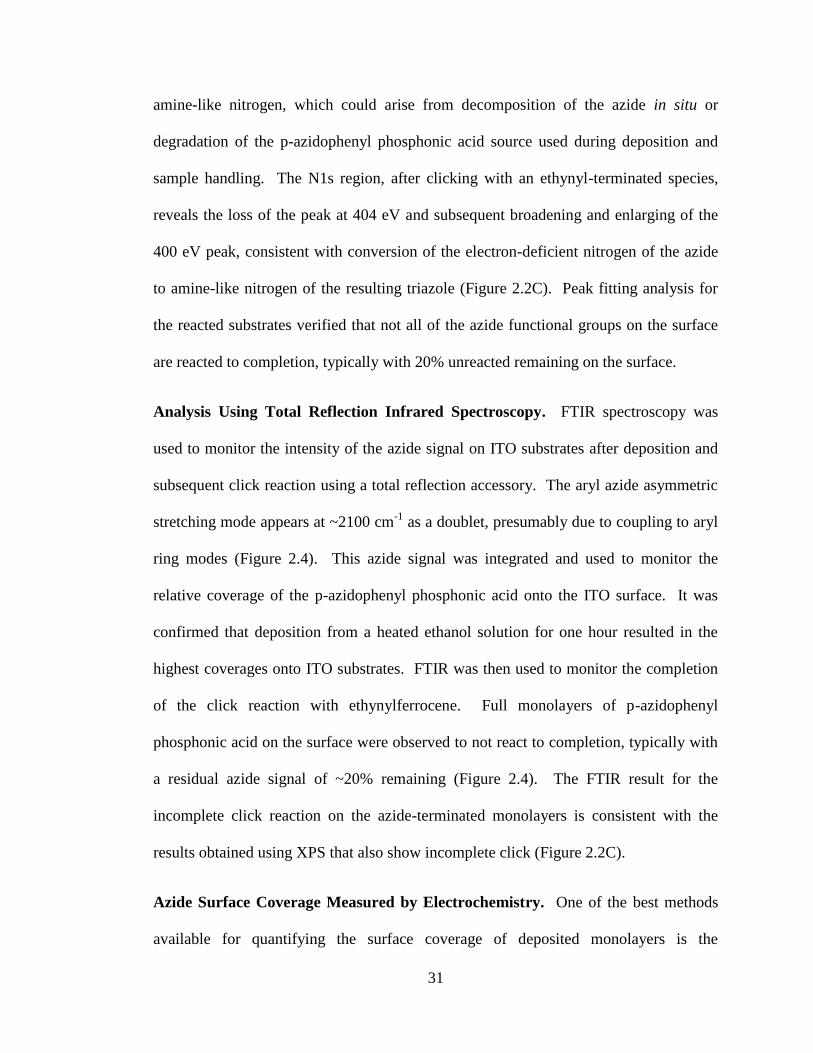
measurement of redox charge by electrochemistry. In this study, ethynylferrocene was
coupled to azide-terminated ITO substrates via the click reaction and used to determine
electrochemical coverage by integration of the current above the background charging
current in cyclic voltammograms (Figure 2.5). The resulting coverage for a full
monolayer of p-azidophenyl phosphonic acid on an ITO substrate clicked with
ethynylferrocene was 7.7(4) x 1013
molecules cm-2
under the deposition conditions
employed. Increasing the exposure time of the azide-terminated ITO substrates to the
click solution to overnight did not result in an increased electrochemical coverage or
further decrease of the azide integration monitored by FTIR. The IR integration of the
azide peak before click was 0.076 cm-1
and after click was 0.016 cm-1
(Figure 2.4).
Thus we conclude that the electrochemical coverage corresponds to (0.076–
0.016)/0.076 80% of the azide groups being clicked with ethynylferrocene. The
expected monolayer coverage for these monolayers would be 7.7 x 10¹³
/80% ≈ 1.0 x
1014
molecules cm-2
. Previous coverages obtained for similar ferrocene-derived
molecules, Fc(COOH) and Fc(CH2)6PO(OH)2, attached to an ITO substrate were
determined to be ~2 x 10¹⁴
molecules cm-2
and 2.7 x 10¹⁴
molecules cm-2
,
respectively.30, 31
The lower than expected coverage obtained for p-azidophenyl phosphonic acid
in this study could be a result of any of the following possibilities: (a) rough surface of
ITO, masking some azide sites while exposing others, (b) clustering or islanding of
azide molecules on the surface due to strong interactive forces between neighboring
molecules or inhomogeneities of surface composition, e.g. lack of exposed Lewis acid
binding sites, which does not allow for an even deposition of molecules, (c) the

33
phosphonic acid molecule oligomerizes on the surface, cross-linking with another
phosphonic acid molecule before reacting with surface hydroxyls, or (d) where the
steric demands of an attached ferrocene to one azide group blocks the catalyst approach
to an adjacent azide group, preventing the click reaction from occurring at the adjacent
site. It is evident that steric constraints play a role as mixed monolayers with lower
azide coverages react to completion, as determined by IR. A pre-clicked solution of
ethynylferrocene with p-azidophenyl phosphonic acid was prepared and deposited onto
an ITO substrate resulting in a coverage of 6 x 10¹³
molecules/cm2. This result suggests
that the low coverage is the result of the lack of Lewis acidic binding sites on the
surface of ITO. Furthermore, the deposition of the p-azidophenyl phosphonic acid onto
a fluorine doped tin oxide substrate (FTO, 4-8 Ω) resulted in lower coverages,
indicating the difficulty in obtaining pure monolayers for species that have to be reacted
to azide-terminated monolayers due to steric constraints.
Mixed Monolayers on ITO. It is common to have some disparity between the mole
fraction of adsorbates in the deposited layer on a substrate and the mole fraction of the
adsorbates in the deposition solution. Each phosphonic acid used could have different
solubilities in the deposition solvent that would potentially affect the kinetics and
thermodynamics of deposition onto surfaces. In this study, IR, XPS and
electrochemistry were used to determine how diluting the p-azidophenyl phosphonic
acid with phenyl phosphonic acid affected adsorption and coverage onto ITO substrates.
Mixtures of the p-azidophenyl phosphonic acid with the diluent phenyl phosphonic acid
were deposited from 1 mM ethanolic solutions that were heated to 80°C for one hour.
The IR, XPS and electrochemical coverage data was plotted against the mole fraction of

34
azide in solution, χazide (Figure 2.7). For each data set, a near linear relationship was
found to exist for the mixed monolayers, indicating deposition of the expected statistical
mixture of the phosphonic acids onto the ITO. This technique could be employed when
a specific coverage of the azide functional group is desired on the surface. Unlike the
pure monolayers of p-azidophenyl phosphonic acid, the samples with 50 % monolayers
were found to react completely with ethynylferrocene resulting in a negligible IR
integration (Figure 2.6A). The coverage of the 50 % monolayer was found to be ~5 x
1013
molecules cm-2
which would correlate well with the inferred full monolayer
coverage of 1.0 x 10¹⁴
molecules cm-2
(Figure 2.6B). This result offers further evidence
that the full monolayer of p-azidophenyl phosphonic acid on the surface is densely
packed in some areas of the surface making it difficult for the bulky catalyst/ligand
complex to approach the next free azide on the surface.
Effect of Water on Monolayer Formation. FTIR was used to study the effect of
water on the adsorption of p-azidophenyl phosphonic acid onto ITO in order to optimize
deposition conditions. It was found that using dry, anhydrous ethanol for the deposition
solvent increased the azide peak as measured by FTIR (Figure 2.8A). This peak
decreased when rinsed with copious amounts of ethanol after removal from the
deposition solution, indicating a large fraction of the p-azidophenyl phosphonic acid
was physisorbed to the surface. The effect of the presence of water during deposition is
not unexpected due to the dehydration reaction that must occur for a phosphonic acid to
deposit on a metal oxide surface. To drive the dehydration of the phosphonic acids that
were physisorbed on the surface after deposition, samples were heated to 105°C for 5-
10 minutes followed by an ethanol rinse to remove any physisorbed molecules. The

35
combination of depositing p-azidophenyl phosphonic acid in anhydrous ethanol
followed by heating the samples and rinsing with ethanol before analysis resulted in the
highest IR signal (Figure 2.8A).
Experiments were also performed to removal of p-azidophenyl phosphonic acid
from the ITO surface. The azide peak obtained after the pure monolayer was formed
from dry ethanol solvent followed by heating in an oven and subsequent rinse with
ethanol was exposed to either an 80°C dry ethanol solvent or an 80°C ethanol/water
(50/50) solvent for one hour. The samples exposed to the dry ethanol solvent had
similar IR integrations while the samples exposed to the ethanol/water solvent lost a
significant amount of azide IR signal (Figure 2.8B). Exposure to an aqueous solvent at
room temperature, however, appeared to have little to no effect on the azide IR signal.
These results highlight the importance keeping the monolayers from being exposed to
elevated temperatures when water is present due to desorption of p-azidophenyl
phosphonic acid from ITO. Samples deposited in dry ethanol and subsequently heated
at 105°C did not produce increased electrochemical coverages with ethynylferrocene.
However, assuming that an IR integration of 0.076 cm-1
corresponds to an
electrochemical coverage of 1.0 x 10¹⁴
molecules cm-2
, an IR integration of 0.15 cm-1
obtained for these samples deposited in dry ethanol, after heating and rinsing, would
correspond to a coverage of 2.0 x 10¹⁴
molecules cm-2
, which is approaching the
expected full monolayer values.14, 15, 32
Stability of the Triazole and Phosphonate/ITO Attachement. A phosphonic acid
molecule was used as the attachment molecule onto ITO due to the stability of the
phosphonate attachment to the surface. Phosphonates attached to metal oxide surfaces

36
are known to attach in a bi- or tri-dentate mode, resulting in a linkage that is stable
under a variety of pH’s, temperatures, and potentials. The exposure of the attachment
to elevated aqueous solutions was found to remove the phosphonate from the ITO
surface (Figure 2.8B). The product after employing the click reaction, a di-substituted
1,2,3-triazole, is thought to be robust while still offering facile electron transfer from an
electroactive species immobilized to the electrode. To test this stability towards
oxidative conditions, p-ethynyl-(trifluoromethyl)benzene was clicked to freshly
prepared azide-terminated monolayers on ITO. Analysis of the N1s, P2p, and F1s
regions by XPS was used to monitor atomic composition before and after being
subjected to an oxidizing potential of 1.5 V vs. Ag/AgCl/KCl in 0.1 M sodium
perchlorate in MeCN. The F1s region of the XPS spectrum indicates that the peak
before and after exposure to the oxidizing conditions were similar (Figure 2.9). Similar
analysis on pure azide-terminated monolayers reveals that the azide signal before and
after exposure to oxidizing conditions remains the same, as measured by FTIR (see
supporting information).

37
2.6: Conclusion
This report highlights the ability to functionalize an ITO surface with p-
azidophenyl phosphonic acid that will allow for coupling of ethynylated compounds
through click chemistry. Deposition of the phosphonic acid from anhydrous ethanol
solutions resulted in the highest inferred coverages. The azide functional group was
clicked with ethynylferrocene resulting in 1,4-disubstituted 1,2,3-triazoles that allowed
for facile electron transfer between the tethered ferrocene molecule and the ITO
electrode. The phosphonate attachment to the surface, and the resulting triazole formed
after the CuAAC reaction, are robust and stable when exposed to a variety of oxidizing
potentials, although the attachment was observed to desorb from the surface when
exposed to elevated temperatures of aqueous solutions. Electrochemical coverages
were found to be short of theoretical monolayers. Despite the lower than expected
coverages obtained, the deposition of p-azidophenyl phosphonic acid resulted in a well-
behaved SAM that is envisioned to provide an oxidatively stable platform for clicking
various ethynyl-terminated electrocatalysts.

38
2.7: Figures
Figure 2.1: Immobilization Schematic. Schematic view of process for immobilizing
the p-azidophenyl phosphonic acid onto an ITO surface. The second step highlights
how the click reaction can be employed to immobilize various ethynyl-terminated
molecules from solution. This strategy allows for a ‘plug and play’ methodology that
will allow various catalysts of interest to be studied electrochemically.

39
Figure 2.2: XPS Analysis. XPS analysis of N1s region of ITO (A) before deposition;
(B) after deposition of p-azidophenyl phosphonic acid; and (C) after clicking the azide
terminated ITO in (B) with ethynylferrocene.
A.
B.
C.

40
Figure 2.3: Deposition of p-Azidophenyl Phosphonic Acid. Deposition of p-
azidophenyl phosphonic acid onto ITO monitored at room temperature () and 80°C ()
by XPS. The areas of the N1s peaks corresponding to the azide were calculated and
normalized to the area of the In3d5 peak using the fitting method described in the text
and supporting materials.

41
Figure 2.4: FTIR Spectrum Before and After Click. IR spectrum of azide region
appearing at ~2100 cm-1
for a monolayer of p-azidophenyl phosphonic acid after
deposition (―) and after clicking with ethynylferrocene (- - -). The remaining azide peak
after click corresponds to ~15-20 % of the unclicked azide integration.
42
Figure 2.5: Cyclic Voltammogram of Clicked Ethynylferrocene. Cyclic
voltammogram of a full monolayer of p-azidophenyl phosphonic acid on ITO clicked
for 3 hours with ethynylferrocene. CV obtained at 1 V/s using a 0.1 M NaClO4 in
MeCN solution. The coverage corresponds to ~8 x 10¹³
molecules/cm2.

43
Figure 2.6: Click Results for Azide-terminated Monolayers. IR (A) and
Electrochemical (B) results obtained after clicking full () and 50% () azide-
terminated monolayers with ethynylferrocene for the given times with the
CuSO4/TTMA catalyst system. The p-azidophenyl phosphonic acids were deposited
with wet ethanol and heated then rinsed before analysis. Electrochemical coverages in
(B) correspond to the value x 1013
molecules/cm2.
A.
B.

44
Figure 2.7: Mixed Monolayers on ITO. Plots of mixed monolayers deposited onto
ITO surfaces for 1 hr at 80°C in 1 mM (azide + diluent) ethanol solutions monitored by
(A) XPS, (B) IR spectroscopy, and (C) electrochemistry (x 1013
molecules/cm2) after
clicking mixed monolayers with ethynylferrocene for 3 hrs. The XPS integration in (A)
was obtained using the fitting method described in the text and in the supporting
materials and normalizing to the In3d5 peak of each sample. The IR integration in (B)
was obtained by integrating the area of the azide peak appearing at ~2100 cm-1
for each
sample. The diluent molecule for each data set was phenyl phosphonic acid.
A.
B.
C.

45
Figure 2.8: Effect of Water on p-Azidophenyl Phosphonic Acid Deposition. (A) IR
integrations of the azide peak under various deposition conditions. No rinsing is for
samples that were removed from the deposition solution and dried in a stream of N2.
Heated samples were placed in an oven at 105-110°C for 5-10 minutes then rinsed
thoroughly with ethanol and dried in a stream of N2. Samples with no heat were
removed from the deposition solution, rinsed thoroughly with ethanol and dried in a
stream of N2. The inferred coverage corresponds to the value that would be expected if
every azide on the surface was reacted with ethynylferrocene. (B) Removal of azide
from the surface by exposure of as deposited samples to dry ethanol and ethanol/water
A.
B.

46
(50/50) at 80°C for one hour.
Figure 2.9: Stability of Azide on ITO Surface. High-resolution scans of the F1s peak
by XPS before (―) and after (- - -) exposure to 1.5 V vs. Ag/AgCl for 5 minutes using a
solution of 0.1 M NaClO4 in MeCN.
47
2.8: References and Notes
1. Porter, M. D.; Bright, T. B.; Allara, D. L.; Chidsey, C. E. D., Spontaneously
organized molecular assemblies. 4. Structural characterization of n-alkyl thiol
monolayers on gold by optical ellipsometry, infrared spectroscopy, and
electrochemistry. J. Am. Chem. Soc. 1987, 109, (12), 3559-3568.
2. Chidsey, C. E. D.; Bertozzi, C. R.; Putvinski, T. M.; Mujsce, A. M.,
Coadsorption of ferrocene-terminated and unsubstituted alkanethiols on gold:
electroactive self-assembled monolayers. J. Am. Chem. Soc. 1990, 112, (11),
4301-4306.
3. Chidsey, C. E. D.; Loiacono, D. N., Chemical functionality in self-assembled
monolayers: structural and electrochemical properties. Langmuir 1990, 6, (3),
682-691.
4. Ulman, A., Formation and Structure of Self-Assembled Monolayers. Chem. Rev.
1996, 96, (4), 1533-1554.
5. Gardner, T. J.; Frisbie, C. D.; Wrighton, M. S., Systems for orthogonal sefl-
assembly of electroactive monolayers on Au and ITO - an approach to molecular
electronics. J. Am. Chem. Soc. 1995, 117, (26), 6927-6933.
6. Armstrong, N. R.; Veneman, P. A.; Ratcliff, E.; Placencia, D.; Brumbach, M.,
Oxide contacts in organic photovoltaics: characterization and control of near-
surface composition in indium-tin oxide (ITO) electrodes. Acc. Chem. Res.
2009, 42, (11), 1748-1757.
7. Carter, C.; Brumbach, M.; Donley, C.; Hreha, R. D.; Marder, S. R.; Domercq,
B.; Yoo, S.; Kippelen, B.; Armstrong, N. R., Small molecule chemisorption on

48
indium-tin oxide surfaces: enhancing probe molecule electron-transfer rates and
the performance of organic light-emitting diodes. J. Phys. Chem. B 2006, 110,
(50), 25191-25202.
8. Yan, C.; Zharnikov, M.; Golzhauser, A.; Grunze, M., Preparation and
characterization of self-assembled monolayers on indium tin oxide. Langmuir
2000, 16, (15), 6208-6215.
9. Mingalyov, P. G.; Lisichkin, G. V., Chemical modification of oxide surfaces
with organophosphorus(v) acids and their esters. Rus. Chem. Rev. 2006, 75, (6),
541-557.
10. Paniagua, S. A.; Hotchkiss, P. J.; Jones, S. C.; Marder, S. R.; Mudalige, A.;
Marrikar, F. S.; Pemberton, J. E.; Armstrong, N. R., Phosphonic acid
modification of indium-tin oxide electrodes: Combined XPS/UPS/contact angle
studies. J. Phys. Chem. C 2008, 112, (21), 7809-7817.
11. Donley, C.; Dunphy, D.; Paine, D.; Carter, C.; Nebesny, K.; Lee, P.; Alloway,
D.; Armstrong, N. R., Characterization of indium-tin oxide interfaces using X-
ray photoelectron spectroscopy and redox processes of a chemisorbed probe
molecule: Effect of surface pretreatment conditions. Langmuir 2002, 18, (2),
450-457.
12. Koh, S. E.; McDonald, K. D.; Holt, D. H.; Dulcey, C. S.; Chaney, J. A.;
Pehrsson, P. E., Phenylphosphonic acid functionalization of indium tin oxide:
Surface chemistry and work functions. Langmuir 2006, 22, (14), 6249-6255.

49
13. Gao, W.; Dickinson, L.; Grozinger, C.; Morin, F.; Reven, L., Self-assembled
monolayers of alkylphosphonic acids on metal oxides. Langmuir 1996, 12, (26),
6429-6435.
14. Clearfield, A.; Smith, G. D., Crystallography and structure of .alpha.-zirconium
bis(monohydrogen orthophosphate) monohydrate. Inorg. Chem. 1969, 8, (3),
431-436.
15. Cao, G.; Hong, H. G.; Mallouk, T. E., Layered metal phosphates and
phosphonates: from crystals to monolayers. Acc. Chem. Res. 1992, 25, (9), 420-
427.
16. Hotchkiss, P. J.; Li, H.; Paramonov, P. B.; Paniagua, S. A.; Jones, S. C.;
Armstrong, N. R.; Bredas, J.-L.; Marder, S. R., Modification of the Surface
Properties of Indium Tin Oxide with Benzylphosphonic Acids: A Joint
Experimental and Theoretical Study. Adv. Mater. 2009, 21, (44), 4496-4501.
17. Paramonov, P. B.; Paniagua, S. A.; Hotchkiss, P. J.; Jones, S. C.; Armstrong, N.
R.; Marder, S. R.; Bredas, J.-L., Theoretical Characterization of the Indium Tin
Oxide Surface and of Its Binding Sites for Adsorption of Phosphonic Acid
Monolayers. Chem. Mater. 2008, 20, (16), 5131-5133.
18. Collman, J. P.; Devaraj, N. K.; Chidsey, C. E. D., "Clicking" functionality onto
electrode surfaces. Langmuir 2004, 20, (4), 1051-1053.
19. Collman, J. P.; Devaraj, N. K.; Eberspacher, T.; Chidsey, C. E. D., Mixed azide-
terminated monolayers: A platform for modifying electrode surfaces. Langmuir
2006, 22, (6), 2457-2464.

50
20. Devaraj, N. K.; Decreau, R. A.; Ebina, W.; Collman, J. P.; Chidsey, C. E. D.,
Rate of interfacial electron transfer through the 1,2,3-triazole linkage. J. Phys.
Chem. B 2006, 110, (32), 15955-15962.
21. Rostovtsev, V.; Green, L.; Fokin, V. V.; Sharpless, K., A stepwise Huisgen
cycloaddition process: Copper(I)-catalyzed regioselective "ligation" of azides
and terminal alkynes. Angew. Chem. Int. Edit. 2002, 41, (14), 2596-2599.
22. Devadoss, A.; Chidsey, C. E. D., Azide-modified graphitic surfaces for covalent
attachment of alkyne-terminated molecules by "click" chemistry. J. Am. Chem.
Soc. 2007, 129, (17), 5370-5372.
23. Zhou, Z.; Fahrni, C., A fluorogenic probe for the copper(I)-catalyzed azide-
alkyne ligation reaction: Modulation of the fluorescence emission via (3)(n,pi*)-
(1)(pi,pi*) inversion. J. Am. Chem. Soc. 2004, 126, (29), 8862-8863.
24. Cooper, R.; Camp, P.; Gordon, R.; Henderson, D.; Henry, D.; Mcnab, H.; De
Silva, S.; Tackley, D.; Tasker, P.; Wight, P., The assembly of rotaxane-like
dye/cyclodextrin/surface complexes on aluminium trihydroxide or goethite.
Dalton Trans. 2006, (23), 2785-2793.
25. Mohapatra, S.; Pramanik, P., Synthesis and stability of functionalized iron oxide
nanoparticles using organophosphorus coupling agents. Colloid Surface A 2009,
339, (1-3), 35-42.
26. Kim, T.; Kim, K., N-Butyllithium-Mediated Reactions of 1-(2-
Azidoarylmethyl)-1H-benzotriazoles with Alkyl Halides. J. Heterocyclic Chem.
2010, 47, (1), 98-111.
51
27. Besbes, S.; Ben Ouada, H.; Davenas, J.; Ponsonnet, L.; Jaffrezic, N.; Alcouffe,
P., Effect of surface treatment and functionalization on the ITO properties for
OLEDs. Mat. Sci. Eng. C-Bio. 2006, 26, (2-3), 505-510.
28. Brumbach, M.; Veneman, P. A.; Marrikar, F. S.; Schulmeyer, T.; Simmonds, A.;
Xia, W.; Lee, P.; Armstrong, N. R., Surface composition and electrical and
electrochemical properties of freshly deposited and acid-etched indium tin oxide
electrodes. Langmuir 2007, 23, (22), 11089-11099.
29. Chaney, J.; Koh, S.; Dulcey, C. S.; Pehrsson, P. E., Surface chemistry of carbon
removal from indium tin oxide by base and plasma treatment, with implications
on hydroxyl termination. Appl. Surf. Sci. 2003, 218, (1-4), 258-266.
30. Zotti, G.; Schiavon, G.; Zecchin, S.; Berlin, A.; Pagani, G., Adsorption of
ferrocene compounds an indium-tin-oxide electrodes. Enhancement of
adsorption by decomposition of ferrocenium molecules by oxygen. Langmuir
1998, 14, (7), 1728-1733.
31. Vercelli, B.; Zotti, G.; Schiavon, G.; Zecchin, S.; Berlin, A., Adsorption of
hexylferrocene phosphonic acid on indium-tin oxide electrodes. Evidence of
strong interchain interactions in ferrocene self-assembled monolayers. Langmuir
2003, 19, (22), 9351-9356.
32. Gui, J. Y.; Stern, D. A.; Lu, F.; Hubbard, A. T., Surface chemistry of 5-
membered heteroaromatics at Pt(111) electrodes studied by EELS, LEED,
Auger-spectroscopy and electrochemistry - furan, pyrrole and thiophene. J.
Electroanal. Chem. 1991, 305, (1), 37-55.

52
2.9: Supporting Information
Cleaning methods for ITO. A number of different cleaning procedures were
investigated in order to increase the surface coverage of the p-azidophenyl phosphonic
acid. The ITO samples were cut into appropriate sizes and rinsed with ethanol followed
by drying in a stream of N2 gas. Some samples were exposed to an oxygen plasma
(90:10 Argon:Oxygen) for up to 10 minutes to remove any adventitious carbon-
containing molecules that might have been on the surface. Other samples were exposed
to the plasma followed by exposure to a mild acid bath. A solvent rinse and sonication
in either ethanol, chloroform or acetone was also investigated for ability to remove any
contaminants from the ITO surface. X-ray photoelectron spectroscopy (XPS) was
performed to determine the atomic composition on the surface. The samples were
analyzed for carbon 1s (C1s), indium 3d5 (In3d5), tin 3d5/2 (Sn3d5/2) and nitrogen 1s
(N1s) with results shown in Figure S1 below. It was found that although the plasma
cleaning appeared to decrease the amount of adventitious carbon, the samples did not
yield increased p-azidophenyl phosphonic acid coverages as measured by Fourier
transform infrared (FTIR) spectroscopy and electrochemistry after clicking with
ethynylferrocene. Results shown in Figure 2S indicate that the deposition on samples
without pretreatment or cleaning yielded the highest coverages. This result appears to
be consistent with the hypothesis that the deposition conditions, an ethanolic solution at
80°C, acted as the best method of cleaning the surface. For this reason the samples used
throughout this study were not pre-cleaned by any technique except an ethanol rinse to
remove any glass pieces and dust that may have been present after cutting the ITO.

53
Peak fitting analysis. A peak fitting procedure was developed to analyze the peaks
appearing at the N1s region of the XPS spectrum related to the azide functional group
of the p-azidophenyl phosphonic acid. Standard mathematical fitting and analysis
software was used to perform the fits and integrations. The method consisted of first
setting a pure Gaussian peak for each of the three nitrogen atoms of an azide functional
group: one for the signal at a binding energy of 404 eV (peak 1) and two within the
signal at a binding energy of 400 eV (peak 2 and peak 3). The peak areas of these three
Gaussian curves were locked to the same area and relative position to each other. Two
additional smaller Gaussian peaks (peak 4 and peak 5) were also used within the signal
at a binding energy of 400 eV to account for any nitrogen contaminates or azide
decomposition products that may have been introduced or formed in the vacuum
chamber of the XPS instrument. Peak 4 and peak 5 were allowed to float in area with
their positions locked. The full-width half-max values and relative peak locations for
all five peaks were also locked with the locations allowed to move as a set due to drift
in the instrument from day to day use. The optimal peak placement for each of the five
Gaussian peaks was determined by addition of many spectra and fitting of this multiple
sample spectrum until the residuals were optimized. The method was completed by
employing a Shirley baseline through the noise of the spectrum that was to be analyzed.
An example of an azide group being fit by this method is shown in Figure S3. The
integration of the N1s region corresponding to the three azide nitrogen atoms was
normalized to the In3d5 peak integration of each sample, which typically remained
within ~10 % range from sample to sample.

54
X-ray decomposition of azide functional group during XPS analysis. Figure S4
below shows the combined integration for all three of the azide peaks, peak 4 area, and
peak 5 area on the same spot of an ITO substrate as a function of scans taken. This
analysis was used to determine the maximum amount of X-ray damage the samples
could withstand in situ while yielding the best signal-to-noise ratio. A maximum of ten
scans was found to be the optimal number of scans for obtaining data before
decomposition of the azide group by X-ray damage during the experiment. The ten
scans were used for each narrow high resolution azide region analysis throughout this
study.
FTIR total reflection accessory. A total reflection accessory was designed and built
for analysis of ITO slides by absorption FTIR spectroscopy. A schematic of the
accessory is shown in Figure S5. The accessory had two gold mirrors angled at 10° to
normal to allow for reflection of light onto and off the sample at a near grazing angle.
The accessory was also equipped with a p-polarizer to filter out s-polarized light. The
samples were placed ITO side down on a 16 mm diameter aperture and scanned 256
times by a deuterated triglycine sulfate (DTGS) detecotor.
Deposition of p-azidophenyl phosphonic acid. Various deposition conditions of the
p-azidophenyl phosphonic acid were attempted in this study. Figure S6 shows the
comparison of depositing the p-azidophenyl phosphonic acid in both ethanol and
tetrahydrofuran solvents (Figure S6A) and from ethanol in the presence of 1 equivalent
of either acetic acid or pyridine present (Figure S6B). It was found that a pure ethanol
deposition yielded the best coverages as determined by IR integration of azide signal

55
and electrochemically by integrating the peak that appeared after clicking with
ethynylferrocene.
Comparison of click conditions. Three click systems were compared in this study to
determine which was most effective at clicking the p-azidophenyl phosphonic acid that
was deposited onto ITO surfaces. The first was a CuSO4 salt in water with no
accelerating ligand, the second a CuSO4 salt with 1.1 equivalents of tris-
(triazolylbenzyl)methyl amine (TBTA) in water, and the third a CuSO4 salt with 1.1
equivalents of TTMA in water. The disappearance of the azide group at ~2100 cm-1
was followed by IR. The integrations were plotted as a function of time of exposure to
the various click reaction catalyst systems. The results are shown in Figure S7. It was
found that the CuSO4/TTMA click system was the most effective, typically being
completed within an hour. The CuSO4/TBTA and CuSO4/no ligand systems click
slowly over time, eventually reaching the values obtained by CuSO4/TTMA system.
Stability of azide on ITO surface. The azide-terminated monolayer was exposed to a
potential bias of 1.5 V vs. Ag/AgCl for 5 minutes in 0.1 M sodium perchlorate in
MeCN. The azide signal was found to decrease slightly by IR after exposure. The
spectra are shown in Figure S8. This result indicates that the attachment is robust for
extended periods of time when exposed to such oxidative conditions.

56
Figure 2.S1. XPS analysis of atomic species on the surface of ITO after cleaning with
the indicated procedures. The carbon percentage decreases with the cleaning
procedures while the relative indium and tin ratios increase. This cleaning did not lead
to improved coverages of p-azidophenylphosphonic acid on the ITO surface however.
Surface Analysis of Cleaned Samples
0
10
20
30
40
50
60
70
Carbon Indium Tin Nitrogen
Atom
Su
rfa
ce
Ato
mic
Pe
rce
nt
Uncleaned
Plasma Cleaned
Plasma + Acid

57
Figure 2.S2. IR spectra of azide region after p-azidophenyl phosphonic acid was
deposited for one hour from a 1 mM ethanolic solution at 80°C on ITO slides that were
uncleaned (), cleaned by oxygen plasma (), and cleaned with oxygen plasma
followed by mild acidic rinse ().

58
Figure 2.S3. Example of XPS peak fitting analysis of N1s region for azide functional
group in this work. Peaks 1, 2, and 3 all correspond to a nitrogen atom within the azide
group and are locked in peak area to each other. Peak 4 corresponds to nitrogen
contamination and peak 5 to a decomposition product of the azide in the chamber. All
peaks are locked to the same full-width at half-max and relative positions to each other,
although they are allowed to float as a set to account for instrument drift.

59
Figure 2.S4. Decomposition of the azide peaks and overall nitrogen signal as a
function of the number of scans taken during an XPS analysis. It was determined that
ten scans were optimal to obtain N1s data while minimizing in situ X-ray damage.

60
Figure 2.S5. Schematic of total reflection accessory used in absorption FTIR
spectroscopy.

61
Figure 2.S6. Representative cyclic voltammograms of p-azidophenyl phosphonic acid
on ITO clicked with ethynylferrocene. The p-azidophenyl phosphonic acid was
deposited (A) without acid or base in ethanol () and THF () and (B) with either one
equivalent of acetic acid () or one equivalent of pyridine () to the azide in ethanol.
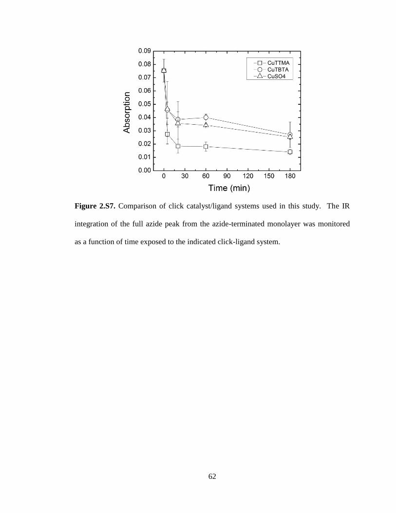
62
Figure 2.S7. Comparison of click catalyst/ligand systems used in this study. The IR
integration of the full azide peak from the azide-terminated monolayer was monitored
as a function of time exposed to the indicated click-ligand system.
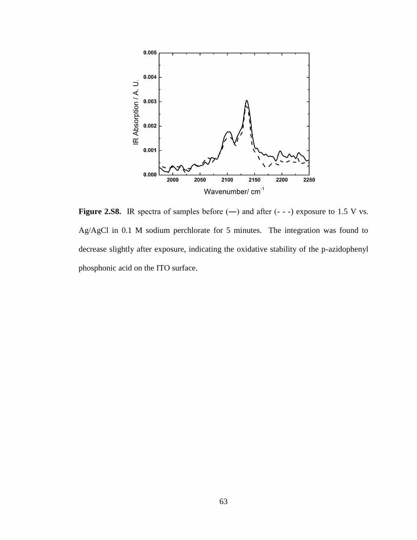
63
Figure 2.S8. IR spectra of samples before (―) and after (- - -) exposure to 1.5 V vs.
Ag/AgCl in 0.1 M sodium perchlorate for 5 minutes. The integration was found to
decrease slightly after exposure, indicating the oxidative stability of the p-azidophenyl
phosphonic acid on the ITO surface.
64
Chapter 3: Introduction
3.1: Abstract
This chapter is as an introduction to the work that was done in Chapters Four
and Five. This work was part of a solar water splitting project in collaboration with
Prof. Paul McIntyre and one of his graduate students, Vincent Chen, of the Materials
Science and Engineering department at Stanford. This chapter will open with a
discussion about the motivating factors behind our work, namely the increasing demand
for clean energy for an increasing world population. Following this will be a short
review of how accomplishing solar water splitting can be achieved, with a focus on
water oxidation at a photoanode. The conclusion of this chapter will introduce some
techniques we used in the following two chapters of my thesis.

65
3.2: The Global Energy Challenge
Meeting the ever-growing demand for energy on a global scale while
simultaneously preserving the environment presents a formidable challenge for
scientists. It is predicted, that by the year 2050, our global energy demand could triple
from our 2010 consumption rate of 15 terawatts (TW) to 45 TW.1 This projection could
vary depending on a number of parameters that include population growth rates, wealth
of these populations (GDP), energy consumption and conservation rates as well as
political concerns. Currently on the global scale, most energy consumed comes from
fossil-based fuel sources (~80%) with the balance being supplemented with
unsustainable bio-mass, nuclear and renewable sources (Figure 3.1A).2 One concern as
the year 2050 approaches is how the predicted 45 TW of global energy demand will be
met (Figure 3.1B).
There are a number of strategies that could be employed to address the rising
global energy demand. Some strategies are more feasible than others while all could be
used in any combination to solve the energy challenge. The first is that people could
start to conserve energy at unprecedented rates. Technology could also play a role by
allowing us to use energy more efficiently. Another strategy is to keep burning fossil-
based fuels at alarming rates and hope that either: (1) nothing happens to the
environment from the resulting carbon dioxide emissions or (2) that adequate carbon
capture and sequestration technologies are developed. Another attractive strategy is to
develop a cheap, carbon-free, renewable source of alternative energy. This could
include any or all of the following sources: solar, hydro-electric, wind, biomass,
geothermal, and tidal. Any of the strategies to be used will also have to meet the base

66
requirement of being both cheap and globally scalable, as to adequately compete with
the currently-used fossil fuel based sources of energy.
The three primary types of fossil fuel based energy are oil, coal and natural gas.
Currently, these energy sources make up the majority of the total global energy
consumption (Figure 3.1A). The high energy density, low cost of use and seemingly
endless supply of these sources (see below) are the main reasons they are currently used
to provide most of our energy. For example, coal is widely considered the cheapest
way to produce electricity at about 1-4 cents per kilowatt hour (kWh) on average.2 The
next cheapest source is natural gas, costing about 2-5 cents per kWh. Oil is the next
cheapest, costing between 6-8 cents per kWh on average. For comparison, the cheapest
renewable source of electricity is wind, which at 5-7 cents per kWh compares favorably
to oil, but cannot compete with coal or natural gas when it comes to how cheaply
electricity can be produced from it. These costs are summarized in Table 3.1 below.
Table 3.1: Cost per kWh for various sources of electricity.2, 3
Source Cost (¢/kWhr) Source Cost (¢/kWhr)
Coal 1-4 Wind 5-7
Natural Gas 2-5 Nuclear 6-7
Oil 6-8 Solar 25-50
To go along with the low cost of electricity production using fossil fuels as the
energy source, there appears to be an abundant supply of these sources. For example, it
is estimated that we have a total (proven and unproven reserves) of about 50-150 years
of oil, 200-600 years of natural gas, and about 2000 years of coal, all based on burn
rates from the year 2000.2 The big error bars associated with these values are due to
availability and ability to obtain these sources, some of which are in remote, hard-to-

67
access regions of the planet. One point that is clear, however, is that we will not run out
of these resources anytime in the immediate future.
In summary, it is clear that the planet will provide many years of fossil fuel
energy for human use. These sources in principle can be used to meet our ever-growing
energy requirements; however, careful consideration for the environmental
consequences of using these sources should be exercised. A more responsible strategy
is to take advantage of the renewable alternative sources of energy, which are not only
abundant and relatively untapped, but also are free of any carbon, and thus do not
produce CO2 when being used.
Renewable and Alternative Sources of Energy
As mentioned above, there are a number of various alternative energy sources
available that could be used in hopes of solving the growing energy demand. Any of
these sources could be used in combination with each other, and each has some obvious
strengths and weaknesses that need to be addressed. The one common theme for all of
these energy sources, however, is that they all produce energy with a minimal amount
of carbon dioxide emissions. Some of these sources produce electricity as a result of
their use, e.g. wind, and some produce a fuel, such as ethanol from sustainable biomass.
The only alternative carbon-free source of energy that can meet our entire future
global energy demand by itself is solar. It has been calculated that sunlight provides
120,000 TW of power that strikes the earth, while an estimated total of 800 TW could
feasibly be collected.2, 4
The most common strategy used to harness solar energy is

68
through the use of photovoltaics (PVs), which are semiconductor materials that will
collect photons which in turn will produce electricity in the form of direct current.
There have been many advancements in the solar industry over the years, but despite
these, PVs are still relatively inefficient, and the cost of the materials used to make PVs
and the cost to install them remains high. As a result, some of the best commercially
available PVs collect incident sunlight with about 10-20% efficiency, while still costing
the user around $300 per square meter.
One drawback of using solar energy as an alternative energy source in any
capacity is the fact that sunlight is intermittent while our energy demands are
continuous. As a peak power source, solar is readily available, as PVs will readily
provide vast quantities of electricity. On cloudy days, or at night, however, electricity
will not be available from PVs. Complicating the matter further is that current
technology does not have a great method to store electricity for off peak use. Currently,
one of the best strategies for storing electricity is pumping water uphill using electricity
obtained by a PV during the day and then letting the water run downhill and through a
turbine at night to get the electricity back. The same idea is used in storing energy by
compressing gas in the day and allowing the gas to expand through a turbine at night.
Batteries and capacitors are a well-known source for energy storage and could also find
use for storing solar energy. Another energy storage mechanism is utilizing chemical
bonds of a fuel. A very promising strategy is to use sunlight to drive the splitting of
water into molecular oxygen and molecular hydrogen, a process known as solar water
splitting. The hydrogen could be used as a fuel source directly, or converted into a
liquid fuel that is easier to use and handle through a few synthetic steps.

69
3.3: Solar Water Splitting
In order to take advantage of all the solar energy that strikes the earth, it is
necessary to store some of the collected daytime sunlight energy for use during the
nighttime. The direct conversion of solar energy to chemical fuels would address this
issue. There are many solar fuel syntheses that, in principle, should work. The best
strategy is performing solar water splitting, which is a process that uses solar energy to
split water to produce molecular oxygen and hydrogen, the ladder of which can be used
as a fuel. There are two common methods employed to accomplish this: (1) using
stable semiconductors to absorb light and create free charge carriers (holes and
electrons) which can be used to split water at the surface/liquid interface, and (2) using
a PV to collect light and create a current, which can be used to run an electrolyzer to
split water. Regardless of the approach taken, any solar water splitting scheme or
system would ultimately have to consist of materials that will collect incident solar
irradiation, generate the appropriate charge carriers and catalyze the oxidation and
reduction of water to make oxygen and hydrogen, respectively, as shown in equation
3.1:
Water oxidation occurs at a standard reversible potential (E°) of 1.23 V versus
the Normal Hydrogen Electrode (NHE) at pH 0. Proton reduction occurs at a standard
reversible potential of 0 V at pH 0, which is the definition of NHE. Both of these
reactions are highly pH dependent as the reversible potentials will shift the Nernstian 59
mV per pH unit change. The kinetic bottleneck of the water splitting reaction has long

70
been considered the water oxidation half reaction of equation 3.1 due to large
overpotentials needed for the reaction to occur. This is due to the necessity of having to
ultimately remove four protons and four electrons from two water molecules with the
subsequent formation of an oxygen-oxygen double bond.
The first requirement of any solar water splitting design is the efficient
absorption of solar irradiation. The solar output spectrum is shown in Figure 3.2, and is
commonly referred to as AM1.5G solar irradiation.5 Materials that can be used in
practical devices and will collect solar irradiation most efficiently are semiconductors.
These are materials that will absorb photons and promote electrons across a bandgap,
which is the energy difference between the valence band and conduction band of the
material. In order to split water, a semiconductor with a minimum bandgap of at least
1.23 eV is needed. Quite often, larger band gaps are required to fulfill water splitting.
These larger band gaps are needed to overcome the overpotential (η) of the water
oxidation and proton reduction reactions. Figure 3.3 depicts a number of band gaps for
some of the more commonly used semiconductors used in solar water splitting setups.6
Semiconductors used for solar water splitting must produce photo-generated
holes oxidizing enough to inject into water to make oxygen while the electrons must
have enough energy to combine with protons to make hydrogen. This can be
accomplished by choosing a semiconductor, or multiple semiconductors, that supply the
proper photovoltage to split water, or by using a catalyst layer attached to a small band
gap semiconductor that allows the band edges to move independently from the solution
when a bias is applied. In either case, the semiconductor must also have a geometry
that will allow a photogenerated charge carrier to migrate through the material and

71
perform the oxidation of water and reduction of protons before thermal recombination
occurs. These destructive recombination pathways are either radiative or nonradiative,
with pathways occurring (1) in the bulk of the semiconductor, (2) in the depletion layer
of the semiconductor, (3) by the majority carrier tunneling through the electric field at
the semiconductor/liquid junction, (4) by the majority carrier thermally escaping the
interfacial barrier and (5) at defect sites within the semiconductor.7 These
recombination pathways, illustrated in Figure 3.4, decrease overall photocurrent, and
thus efficiency, that could otherwise be obtained by the device.
The bandgap of a semiconductor must also not be too large in order to split
water with any efficiency. This is because all semiconductors collecting light with
energy greater than the bandgap will experience thermalization losses from carriers
relaxing to the band edge.8 As a general rule of thumb, a good photovoltaic device will
generate at most about two-thirds of its band gap in photovoltage at 1 sun illumination.
The system reported by Honda and Fujishima, which uses titanium dioxide (bandgap =
3.0 eV) as the semiconductor, is restricted to the UV portion of the solar spectrum and
limits the total current density that can be obtained to a maximum of 2 mA/cm2.9 The
maximum efficiency of any photovoltaic design, whether a single semiconductor or
multi-junction setup, is governed by both the fraction of solar energy absorbed and
photovoltage obtained. Both of these parameters are related to the bandgap of the
material(s) used. Even with the best catalysts used for water splitting, the
overpotentials associated with water oxidation and reduction at 1 sun illumination
would still add an additional voltage (~few hundred millivolts, see Table 3.4) to the
potential needed, bringing the total to ~1.7 V to 2.0 V to obtain reasonable current
72
densities. As a result, a single semiconductor used for solar water splitting, without any
additional energy input, must have a bandgap of at least ~1.7 to 2.0 eV with the band
edges straddling the water oxidation and proton reduction potentials plus associated
overpotentials. These larger bandgap requirements result in less absorption of the solar
spectrum, lowering the operating efficiency from about a 30% theoretical maximum to
that of about 10%. The solar-to-hydrogen efficiency (ε) for any photoelectrolysis cell
can be calculated using equation 3.2 below:
(3.2)
where Jm is the measured current density (A/cm2), Vapp is the applied potential (V)
measured between the photoanode and photocathode and Pin (W/cm2) is the input power
density of the solar illumination.11
These calculations should be conducted based off
results obtained when the solar water splitting cell is investigated as part of a two
electrode setup. Band diagrams for several possible water splitting schemes utilizing
solar irradiation as the only energy input are shown in Figure 3.4.
In order to make a useful solar water splitting device to be used on a global
scale, a material must be found, or designed, that simultaneously meets all the following
criteria: (1) efficiently absorbs a large fraction of the solar spectrum, (2) proper bandgap
energy alignment that allows for water oxidation and proton reduction, (3) adequately
allows charge transfer of photogenerated minority carriers to the surface/liquid
interface, (4) efficiently catalyzes water oxidation and proton reduction at the interface,
(5) remains stable during operating conditions at any pH and very oxidizing
environments for water oxidation, (6) made out of abundant and cheap materials, and

73
(7) is non-toxic. To date, there has not been a material discovered or designed that
simultaneously meets all of these criteria. There have only been a few photoanode
unassisted water splitting systems discovered which can use sunlight as the only energy
input to drive the water splitting reaction.12-15
Other promising water splitting designs include multi-junction semiconductors
in ohmic contact with each other. A factor of two hit in theoretical efficiency is
suffered for each junction due to minority charge carrier recombination at the interfaces.
Therefore, for example, a theoretical maximum efficiency of 15% would be obtained
for a two semiconductor, single p-n junction setup used for splitting water.10
The multi-
junction design reported by Turner was shown to catalyze water splitting with an
overall efficiency of 12.4 %.16
Unfortunately, this setup utilizes expensive materials to
operate, which are neither scalable nor robust for any extended periods of operation.
Current research efforts have broadly focused on finding cheap and abundant materials
that can support rapid charge transfer at the semiconductor/liquid interface, have
substantial durability under operating conditions and absorb a larger fraction of the solar
spectrum.
The idea of using sunlight to split water is not a new concept, as plants have
been accomplishing this feat since their existence. As has been shown above, there
remains many challenges to eventually making a commercially viable system that
works with cheap materials over an extended period of time. With the development or
discovery of a new semiconductor material that could be used toward solar water
splitting, an efficient water oxidation catalyst must be coupled either directly or through
a wire to accomplish the production of oxygen and hydrogen. The next topic of this

74
chapter will introduce some water oxidation catalysts that could be employed in a solar
water splitting device.
Photoanodes and Water Oxidation Catalysts
One of the best strategies to address the low efficiency of photoelectrochemical
water splitting cells is through the incorporation of more efficient water oxidation
catalysts. As mentioned above, the water oxidation reaction of equation 3.1 is often the
kinetic bottleneck for water splitting due to the large overpotentials commonly
associated with the reaction. Catalysts that can more efficiently remove four electrons
from water while forming the oxygen-oxygen double bond can be incorporated onto a
semiconductor material which should improve the overall device efficiency. There has
been much focus on the design and development of new water oxidation catalysts,
ranging from discrete transition metal-based homogeneous catalysts17-21
, metal and
metal oxide films22-24
and combinations of immobilized catalysts on
semiconductor/electrode surfaces25, 26
.
This introductory chapter will focus mainly on heterogeneous metal and metal
oxide water splitting catalysts in favor of discrete homogeneous catalysts. The most
active and best performing water oxidation catalysts to date are metal and metal oxides
of iridium and ruthenium. The problem with these metals, however, is their associated
high costs, which limit their applicability for large scale use. Table 3.2 below
summarizes the overpotential (η) required to obtain 1 mA/cm2 current density for some
of the common metal and metal oxide catalysts employed for water oxidation. This
table is not exhaustive for all water oxidation catalysts that are known and the reader
should consult some of the relevant reviews on this topic for a more extensive list.27, 28

75
Table 3.2: Various water oxidation catalysts and their performance at i = 1 mA/cm2.
Catalyst E, V vs. NHE η, V pH Ref
Ru
RuO2 1.43 0.2 0 29, 30
Ru-Ir 1.52 0.294 0 31a
Ru-Pt 1.7 0.474 0 31a
Ir
Ir 1.55 0.324 0 31a
IrO2 (planar) 1.42 0.561 6.3 23
IrO2 (particle) 1.39 0.473 5.3 32
IrO2 (particle) 1.12 ~0.3 7 22, 33
Ir-Pt 1.6 0.374 0 31a
Pt
Pt 1.94 0.714 0 31a
PtO2 1.042 0.638 0 34
Co
Co-Phosphate 1.24 0.41 7 24
Co3O4 0.844 0.44 14 35
Other Metals
NiOx 0.509 0.235 16.2 31a
MnO2 1.37 0.2 13 36
Semiconductors
Fe2O3 (dark) 1.83 0.6 14 37
Fe2O3 (light) 1.1 -0.13 14 37
WO3 (dark) 1.85 1.03 7 38
WO3 (light) 0.9 0.496 0 39 a Measured at 80°C
The overpotentials given in Table 3.4 were calculated by taking the difference from the
measured potential versus NHE and the theoretical reversible potential, E°, which can
be calculated by substituting the given pH into equation 3.3.
E° = 1.23 V – (0.059 V) pH vs. NHE (3.3)
If Table 3.4 is any indication, the amount of materials studied for efficient water
oxidation is quite extensive and thorough. If a new catalyst system cannot be found, the
only option left is to find methods to incorporate minimal amounts of the best
performing catalysts, iridium or ruthenium, onto a stable semiconductor employed in
solar water splitting. Simply putting a good water oxidation catalyst on a

76
semiconductor, however, does not allow for a device to be operational in solar water
splitting. The semiconductor must often be protected from the harsh environments of
the water splitting reaction, namely oxidizing potentials and extreme pH’s. The next
section of this chapter will discuss some methods for protecting semiconductors during
operation in solar water splitting.
Protection of Photoanodes Used in Solar Water Splitting
A critical component of any photoelectrochemical water splitting device that
utilizes a water oxidation catalyst attached to a photon absorbing semiconductor
substrate is operational stability. As has been discussed, the water oxidation reaction is
an oxidatively demanding reaction often occurring in harsh pH and oxidative
environments. The harsh conditions often employed for photoelectrochemical water
oxidation at a photoanode will typically oxidize the photon absorbing semiconductor
before water. In the case of silicon as the photoanode, the silicon will oxidize to silicon
dioxide which is an insulating material that doesn’t conduct. In other cases, the
semiconductor will slowly dissolve into the water over time. Since avoiding the water
oxidation reaction at the anode surface is impossible for a photoanode with small
enough bandgaps to harvest an optimal fraction of the solar spectrum, a material must
be used to protect the underlying base substrate. A good protecting layer must be
utilized that meets the following criteria: (1) adequately protects the semiconductor
from corrosion, or oxidation, (2) allows for efficient transfer of holes and electrons
between the semiconductor and catalyst, and (3) does not absorb much light. If the
protection layer absorbs a large fraction of light it will decrease the amount of photons
able to reach the semiconductor, which will decrease the photocurrent and efficiency

77
that could otherwise be obtained. Previous attempts at protecting semiconductors used
as photoanodes have included depositing thick layers of oxidized protective coatings on
the photoanode that prevent the semiconductor surface from being exposed to oxides
that are generated during water oxidation.40
These thick coatings often decrease device
efficiency, as they would not allow facile electron transport or would absorb solar
irradiation themselves and act as the semiconductor instead of the substrate they were
employed to protect. Some methods also include thin layers of protective coatings.41
These often suffered stability issues as the coatings were typically too thin to be
uniform, which would allow for oxide migration and thus corrosion of the underlying
semiconductors. Other methods have included doping ruthenium into titanium dioxide
electrodes. The ruthenium helps the titanium dioxide become more conducting and acts
as a catalyst, while the titanium dioxide provides stability for the ruthenium. These
devices are known as dimensionally stable anodes, and are commonly employed in the
chloro-alkaline industry for the production of chlorine gas and more recently water
oxidation to produce oxygen; unfortunately these types of coatings are expensive
because the noble metal must be present throughout the thickness of the thick titanium
dioxide films.42-45
In the next two chapters, a new method will be introduced that accomplishes the
protection of a small band gap base semiconductor during photoelectrochemical water
splitting while not decreasing efficiency. We utilized a thin layer of titanium dioxide
(TiO2) that acts as a corrosion barrier to an underlying semiconductor while still
allowing for facile charge transport between it and the catalyst layer on top of the
structure that was used in water oxidation. The method used to deposit thin conformal

78
layers of TiO2 was atomic layer deposition (ALD). This technique will cycle between a
titanium precursor and water to create a single layer of TiO2 on a surface. The cycles
can be repeated until the desired thickness is obtained, resulting in a uniform thickness
that is free of pinholes or cracks.

79
3.4: Figures
Figure 3.1: Current and Future Global Energy Demand. Pie charts depicting global
energy use in terawatts for each energy source in both (A) 2010 at 15 TW total energy
and (B) 2050 at 45 TW total energy. The 2050 pie chart is a projection based off of the
discussion from the text and already has the energy sources from 2010 added in. The
additional 30 TW of energy consumption remains to be filled in.
A. B.

80
Figure 3.2: Solar Spectrum. Solar irradiance spectrum as detected at the Earth’s
surface, referred to as AM1.5G solar irradiation.5

81
Figure 3.3: Band Gaps of Common Semiconductors. Commonly used
semiconductors employed in photoelectrochemical water splitting devices and their
band gaps. Horizontal lines represent the standard reduction potentials for proton
reduction and water oxidation. A photoelectrochemical cell utilizing one
semiconductor material that only uses solar irradiation to drive water splitting must
have a band gap that straddles these horizontal lines, plus any additional overpotentials
necessary to catalyze each reaction.6

82
Figure 3.4: Recombination Pathways for Photogenerated Electron/Hole Pairs. (A)
An electron of a n-type semiconductor absorbing a photon to create an electron/hole
pair within the depletion region. In an ideal case the hole will travel to the
semiconductor/liquid interface and the electron to the backside contact because of the
band bending that occurs due to the dipole created at the surface. (B) Illustration of
possible pathways for loss of photocurrent due to (1) electron/hole recombination
within the bulk of the semiconductor, (2) electron/hole recombination within the
depletion region of the semiconductor, (3) electron tunneling across the junction to
some acceptor in solution, (4) thermal relaxation of electron across barrier due to
excitation above the potential barrier (thermionic emission), and (5) electron/hole
recombination at defect sites within the semiconductor or at the interface.

83
Figure 3.5: Photoelectrochemical Water Splitting Configurations. Possible
configurations of anodes, cathodes and PV’s that will perform water splitting without
the input of external bias. The setup employed in (A) is a single photoanode material
that has a band gap of at least 1.23 eV and can split water. The PV-photoanode in (B)
describes a setup that requires a photovoltaic material in series with the photoanode
material to reach the required 1.23 eV bandgap. This would require 2 photons absorbed
for every electron used to reduce protons. The setup shown in (C) indicates a solar cell
which uses a photoanode and photocathode to reach 1.23 eV. This arrangement would
also require the collection of two photons for each electron used in proton reduction.
A. B.
C.

84
3.5: References
1. Lewis, N. S.; Nocera, D. G., Powering the planet: Chemical challenges in solar
energy utilization. Proc. Natl. Acad. Sci. 2006, 103, (43), 15729-15735.
2. Lewis, N. S., Powering the planet. MRS Bull. 2007, 32, (10), 808-820.
3. World Energy Assessment: Energy and the Challenge of Sustainability.
http://www.undp.org/energy/activities/wea/drafts-frame.html
4. Cook, T. R.; Dogutan, D. K.; Reece, S. Y.; Surendranath, Y.; Teets, T. S.;
Nocera, D. G., Solar Energy Supply and Storage for the Legacy and Non legacy
Worlds. Chem. Rev. 2010, 110, (11), 6474-6502.
5. ERDA/NASA -1022/77/16 1977.
6. Kudo, A.; Miseki, Y., Heterogeneous photocatalyst materials for water splitting.
Chem. Soc. Rev. 2009, 38, (1), 253-278.
7. Walter, M. G.; Warren, E. L.; McKone, J. R.; Boettcher, S. W.; Mi, Q. X.;
Santori, E. A.; Lewis, N. S., Solar Water Splitting Cells. Chem. Rev. 2010, 110,
(11), 6446-6473.
8. Shockley, W.; Queisser, H. J., Detailed Balance Limit of Efficiency of p-n
Junction Solar Cells. J. of Applied Phys. 1961, 32, (3), 510-519.
9. Fujishima, A.; Honda, K., Electrochemical Photolysis of Water at a
Semiconductor Electrode. Nature 1972, 238, (5358), 37-38.
10. Varghese, O. K.; Grimes, C. A., Appropriate strategies for determining the
photoconversion efficiency of water photo electrolysis cells: A review with
examples using titania nanotube array photoanodes. Sol. Energ. Mat. Sol. C
2008, 92, (4), 374-384.

85
11. Chen, Z.; Jaramillo, T. F.; Deutsch, T. G.; Kleiman-Shwarsctein, A.; Forman, A.
J.; Gaillard, N.; Garland, R.; Takanabe, K.; Heske, C.; Sunkara, M.; McFarland,
E. W.; Domen, K.; Miller, E. L.; Turner, J. A.; Dinh, H. N., Accelerating
materials development for photoelectrochemical hydrogen production:
Standards for methods, definitions, and reporting protocols. J. Mater. Res. 2010,
25, (1), 3-16.
12. Morisaki, H.; Watanabe, T.; Iwase, M.; Yazawa, K., Photoelectrolysis of Water
with TiO2 Covered Solar Cell Electrodes. Appl. Phys. Lett. 1976, 29, (6), 338-
340.
13. Wagner, F.; Somorjai, G., Photocatalytic and Photoelectrochemical Hydrogen
Production on Strontium Titanate Single Crystals. J. Am. Chem. Soc. 1980, 102,
(17), 5494-5502.
14. Sato, J.; Saito, N.; Yamada, Y.; Maeda, K.; Takata, T.; Kondo, J.; Hara, M.;
Kobayashi, H.; Domen, K.; Inoue, Y., RuO2-loaded beta-Ge3N4 as a non-oxide
photocatalyst for overall water splitting. J. Am. Chem. Soc. 2005, 127, (12),
4150-4151.
15. Waki, I.; Cohen, D.; Lal, R.; Mishra, U.; DenBaars, S. P.; Nakamura, S., Direct
Water Photoelectrolysis with Patterned n-GaN. Appl. Phys. Lett. 2007, 91, (9),
093519.
16. Khaselev, O.; Turner, J., A monolithic photovoltaic-photoelectrochemical
device for hydrogen production via water splitting. Science 1998, 280, (5362),
425-427.

86
17. Gersten, S. W.; Samuels, G. J.; Meyer, T. J., Catayltic Oxidation of Water by an
Oxo-Bridged Ruthenium Dimer. J. Am. Chem. Soc. 1982, 104, (14), 4029-4030.
18. Lebeau, E. L.; Adeyemi, S. A.; Meyer, T. J., Water Oxidation by
[(tpy)(H2O)2RuIIIORuIII(H2O)2(tpy)]4+. Inorg. Chem. 1998, 37, (25), 6476-
6484.
19. Sala, X.; Romero, I.; Rodriguez, M.; Escriche, L.; LLOBET, A., Molecular
Catalysts that Oxidize Water to Dioxygen. Angew Chem Int Edit 2009, 48, (16),
2842-2852.
20. Zong, R.; Thummel, R., A new family of Ru complexes for water oxidation. J.
Am. Chem. Soc. 2005, 127, (37), 12802-12803.
21. McDaniel, N. D.; Coughlin, F. J.; Tinker, L. L.; Bernhard, S., Cyclometalated
iridium(III) aquo complexes: Efficient and tunable catalysts for the
homogeneous oxidation of water. J. Am. Chem. Soc. 2008, 130, (1), 210-217.
22. Nakagawa, T.; Beasley, C. A.; Murray, R. W., Efficient Electro-Oxidation of
Water near Its Reversible Potential by a Mesoporous IrOx Nanoparticle Film. J.
Phys. Chem. C 2009, 113, (30), 12958-12961.
23. Yagi, M.; Tomita, E.; Kuwabara, T., Remarkably high activity of
electrodeposited IrO2 film for electrocatalytic water oxidation. J. Electroanal.
Chem. 2005, 579, (1), 83-88.
24. Kanan, M. W.; Nocera, D. G., In situ formation of an oxygen-evolving catalyst
in neutral water containing phosphate and Co2+
. Science 2008, 321, (5892),
1072-1075.

87
25. Francas, L.; Sala, X.; Benet-Buchholz, J.; Escriche, L.; LLOBET, A., A Ru-
Hbpp-Based Water-Oxidation Catalyst Anchored on Rutile TiO2. Chemsuschem
2009, 2, (4), 321-329.
26. Chen, Z.; Concepcion, J. J.; Jurss, J. W.; Meyer, T. J., Single-Site, Catalytic
Water Oxidation on Oxide Surfaces. J. Am. Chem. Soc. 2009, 131, (43), 15580-
15582.
27. Matsumoto, Y.; Sato, E., Electrocatalytic properties of transition metal oxides
for oxygen evolution reaction. Materials Chemistry and Physics 1986, 14, (5),
397-426.
28. Brimblecombe, R.; Dismukes, G. C.; Swiegers, G. F.; Spiccia, L., Molecular
water-oxidation catalysts for photoelectrochemical cells. Dalton Trans. 2009,
(43), 9374-9384.
29. Lodi, G.; Sivieri, E.; Debattisti, A.; Trasatti, S., Ruthenium Dioxide Based Film
Electrodes. 3. Effect of Chemical Composition and Surface Morphology on
Oxygen Evolution in Acid Solutions. J. Appl. Electrochem. 1978, 8, (2), 135-
143.
30. Neumannspallart, M.; Kalyanasundaram, K.; Gratzel, C.; Gratzel, M.,
Ruthenium Dioxide Electrodes as Suitable Anodes for Water Photolysis. Helv.
Chim. Acta. 1980, 63, (5), 1111-1118.
31. Miles, M. H.; Klaus, E. A.; Gunn, B. P.; Locker, J. R.; Serafin, W. E., Oxygen
Evolution Reaction on Platinum, Iridium, Ruthenium and their Alloys at 80
Degrees C in Acid Solutions. Electrochimica Acta 1978, 23, (6), 521-526.

88
32. Yagi, M.; Tomita, E.; Sakita, S.; Kuwabara, T.; Nagai, K., Self-assembly of
active IrO2 colloid catalyst on an ITO electrode for efficient electrochemical
water oxidation. J. Phys. Chem. B 2005, 109, (46), 21489-21491.
33. Nakagawa, T.; Bjorge, N. S.; Murray, R. W., Electrogenerated IrOx
Nanoparticles as Dissolved Redox Catalysts for Water Oxidation. J. Am. Chem.
Soc. 2009, 131, (43), 15578-15580.
34. Iwakura, C.; Fukuda, K.; Tamura, H., Anodic Evolution of Oxygen on Platinum
Oxide Electrode in Alkaline Solutions. Electrochimica Acta 1976, 21, (7), 501-
508.
35. Iwakura, C.; Honji, A.; Tamura, H., The Anodic Evolution of Oxygen on
Co3O4 Film Electrodes in Alkaline Solutions. Electrochimica Acta 1981, 26,
(9), 1319-1326.
36. Gorlin, Y.; Jaramillo, T. F., A Bifunctional Nonprecious Metal Catalyst for
Oxygen Reduction and Water Oxidation. J. Am. Chem. Soc. 2010, 132, (39),
13612-13614.
37. Kay, A.; Cesar, I.; Graetzel, M., New benchmark for water photooxidation by
nanostructured alpha-Fe2O3 films. J. Am. Chem. Soc. 2006, 128, (49), 15714-
15721.
38. Seabold, J. A.; Choi, K.-S., Effect of a Cobalt-Based Oxygen Evolution Catalyst
on the Stability and the Selectivity of Photo-Oxidation Reactions of a WO3
Photoanode. Chem. Mater. 2011, 23, (5), 1105-1112.
89
39. Santato, C.; Ulmann, M.; Augustynski, J., Photoelectrochemical properties of
nanostructured tungsten trioxide films. J. Phys. Chem. B 2001, 105, (5), 936-
940.
40. Kohl, P. A.; Frank, S. N.; Bard, A. J., Semiconductor Electrodes. 11. Behavior
of n-Type and p-Type Single Crystal Semiconductors Covered with Thin
Normal TiO2 Films. J. Electrochem. Soc. 1977, 124, (2), 225-229.
41. Decker, F.; Fracastorodecker, M.; Badawy, W.; Doblhofer, K.; Gerischer, H.,
The Photocurrent Voltage Characteristics of the Heterojunction Combination n-
Si/SnO2/Redox Electrolyte. J. Electrochem. Soc. 1983, 130, (11), 2173-2179.
42. Chen, X.; Chen, G., Stable Ti/RuO2-Sb2O5-SnO2 electrodes for O-2 evolution.
Electrochimica Acta 2005, 50, (20), 4155-4159.
43. Cipris, D.; Pouli, D., Oxygen Evolution on Dimensionally Stable Anode
Materials. J. Electroanal. Chem. 1976, 73, (1), 125-128.
44. Cornell, A.; Hakansson, B.; Lindbergh, G., Ruthenium-based dimensionally
stable anode in chlorate electrolysis - Effects of electrolyte composition on the
anode potential. J. Electrochem. Soc. 2003, 150, (1), D6-D12.
45. Ouattara, L.; Diaco, T.; Duo, I.; Panizza, M.; Foti, G.; Comninellis, C.,
Dimensionally stable anode-type anode based on conductive p-silicon substrate.
J. Electrochem. Soc. 2003, 150, (2), D41-D45.

90
Chapter 4: Stable Si Photoanodes for Water Splitting
4.1: Preface
This work was done in collaboration with with Professor Paul C. McIntyre and
his student, Yi Wei (Vincent) Chen, and was recently submitted and accepted for
publication to the journal Nature Materials and reprinted here with permission.1
Vincent and I helped design and perform the experiments and analyzed the results and
prepared the manuscript. I would like to thank Jung-Yong Lee, Rostam Dinyari, and
Prof. Peter Peumans for providing access to the solar simulation setup. I also thank
Prof. Thomas Jaramillo, Dr. Shin-Jung Choi, Kendra Kuhl, and Blaise Pinaud for
impedence spectroscopy and reversible hydrogen electrode measurements, as well as
their many helpful discussions. I also thank Dr. Byungha Shin and Dr. Michael
Shandalov for their help in TiO2 deposition and characterization. This work was
partially supported by the Stanford Global Climate and Energy Project. I would also
like to acknowledge the Center for Integrated Systems and a Precourt Institute for
Energy seed grant for funding for this work.
1. Chen, Y. W.; Prange, J. D.; Duehnen, S.; Park, Y.; Gunji, M.; Chidsey, C. E. D.;
McIntyre, P. C., Atomic layer-deposited tunnel oxide stabilizes silicon photoanodes
for water oxidation. Nature Mat. 2011, 10, 539-544.

91
4.2: Abstract
A leading approach for large-scale electrochemical energy production with
minimal global-warming gas emission is to use a renewable source of electricity, such
as solar energy, to oxidize water, providing an abundant source of electrons needed in
fuel synthesis. We report corrosion-resistant, nanocomposite anodes for the oxidation of
water required to produce renewable fuels. Silicon (Si), an earth-abundant element and
an efficient photovoltaic material, is protected by atomic layer deposition (ALD) of a
highly uniform, 2 nm thick layer of titanium dioxide (TiO2) and then coated with an
optically transmitting layer of a known catalyst (3 nm iridium). Photoelectrochemical
water oxidation was observed to occur below the reversible potential while dark
electrochemical water oxidation was found to have low-to-moderate overpotentials at
all pH values, resulting in an inferred photovoltage of ~550 mV. Water oxidation is
sustained at these anodes for many hours in harsh pH and oxidative environments
whereas comparable silicon anodes without the TiO2 coating quickly fail. The desirable
electrochemical efficiency and corrosion resistance of these anodes is made possible by
the low electron-tunneling resistance (< 0.006 Ω cm2 for p
+-Si) and uniform thickness
of atomic-layer deposited TiO2.
92
4.3: Introduction
Rising global energy demand and a growing concern for the climate promote
interest in new technologies to harness energy from renewable sources while decreasing
dependence on fossil fuels.1 One interesting approach is to produce hydrogen or other
reduced molecular fuels from intermittent energy sources such as solar and wind.1,2
Electrons needed for renewable fuel production at large scale are likely to come from
the oxidation of water:
298Kat NHE vs.pH V 059.0V 23.1 -e 4 HA4 O-A 4 O H22
O22
E
where the base, A-, and reversible electrochemical potential,
2OE , are determined by the
composition and pH of the system. Water oxidation is a demanding electrochemical
reaction requiring oxidatively robust, and yet inexpensive, anodes. One strategy to
reduce costs is to combine the solar harvesting properties of a photovoltaic with water
oxidation in the form of a photoanode. Here, we report on a novel method of
passivating the surface of an otherwise unstable photoanode material (Si) for operation
in an aqueous electrolyte solution. The protected photoanode both absorbs solar
photons and provides holes in its valence band to oxidize water to molecular oxygen, as
illustrated in Figure 1A.
Due to its stability over a range of pH and potentials, titanium dioxide (TiO2) is
a useful photoanode material.3 Although the large bandgap of TiO2 (~3 eV) permits
photooxidation of water in the absence of an applied bias, it limits absorption to the
small fraction of the solar spectrum in the ultraviolet, resulting in low efficiency as a
solar photoanode.4 Photoanodes such as iron oxide (Fe2O3, bandgap 2.3 eV) and
tungsten oxide (WO3, bandgap 2.7 eV) semiconductors have also been shown to
93
perform water oxidation, and are both considered to be promising in dual bandgap water
splitting cells.5 However, these materials are limited to lower saturation current
densities at higher applied biases due to their modest electronic conductivity and
moderate bandgaps.6,7
Many small bandgap semiconductor photoanodes, such as Si
(bandgap 1.1 eV), are capable of absorbing a large portion of the solar spectrum, but are
not stable at the highly oxidative potentials required for water oxidation.8
An inexpensive and easily synthesized corrosion-resistant layer that protects the
underlying semiconductor while not inhibiting charge carrier (electron or hole) transport
and photon absorption would be highly desirable. Previous attempts at passivating Si
photoanodes with protective noble metal and noble metal silicide layers9,10
, or by
doping the SiO2 layer on Si for better conductivity11
, were unsuccessful in obtaining a
high performance, long-lasting water oxidation photoanode. Attempts at protecting Si
photoanodes with TiO2 deposited by chemical vapor deposition (CVD) were also
unsuccessful.12
Titanium oxide layers thick enough to avoid the dissolution of the
underlying substrate through pinholes or cracks were found to inhibit electron transfer
from the electrolyte to the substrate, resulting in poor water oxidation performance.12
Passivation of compound semiconductors, such as CdSe and CuO, with TiO2 or other
materials was also attempted but was also unable to simultaneously achieve long
endurance and good conversion efficiency for water oxidation.13-15
Using methods from state-of-the-art semiconductor electronics technology, we
have combined the best properties of TiO2 and Si to synthesize an oxidatively robust
and efficient photoanode for water oxidation. In this work, as-received Si substrates
with an initial SiO2 surface layer were coated with a pinhole-free layer of TiO2 by

94
atomic layer deposition (ALD).16
A TiO2 thickness of 2 nm was found to prevent
oxidation of the Si while being thin enough to allow facile electron tunneling between
an overlying catalyst layer and the base substrate. Iridium, one of many well-known
metal and metal oxide catalysts that promote efficient water oxidation over a range of
pH17-21
, was deposited on top of the TiO2 layer by physical vapor deposition (PVD)
methods. An Ir film 3 nm thick was found to be a sufficient amount of catalyst while
not blocking the transmission of photons into the Si substrate. A schematic
representation of the nanocomposite structure of the optimized anode is shown in Figure
4.1A. Figures 4.1B and C show a cross-sectional transmission electron micrograph
(TEM) and a schematic band diagram of the photoanode structure, respectively.

95
4.4: Results and Discussion
Lightly phosphorus-doped n-type Si wafers (n-Si, 0.1-0.2 cm, 500 μm
thickness) were used as the base substrate, onto which 24 cycles of ALD-TiO2 (2 nm)
and 3 nm of PVD-Ir were sequentially deposited (Ir/TiO2/n-Si). Water oxidation
currents at these nanocomposite anodes were measured as a function of potential with
and without simulated solar irradiation at 1 sun (AM1.5G) in acidic (1 M H2SO4),
neutral (1 M phosphate-buffered, pH 7) and basic (1 M NaOH) solutions (Figure
4.1D). Electron transfer from Ir to Si through the oxide layers fills photogenerated
holes in the Si valence band. Electrons are re-supplied to the Ir layer via the water
oxidation reaction. With n-type Si substrates in the dark, which have a very low thermal
population of holes, modest overpotentials for water oxidation produced minimal
currents (of order A/cm2). With illumination, which produces photo-generated holes in
the Si substrate, current densities at all pH values increased dramatically. The potential
required to obtain 1 mA/cm2 was observed to be ~200 mV lower than the
thermodynamic water oxidation potential as a result of the additional voltage made
available by the photo-generated holes (Table 4.1). This onset potential is similar to
that of the best reported values for Fe2O3 and WO3 photoanodes.6,7
However, the
smaller bandgap of Si and its relatively large carrier mobilities allow the nanocomposite
anode to achieve much higher current densities at biases exceeding the onset potential.
Tafel slopes for the nanocomposite anode were found to be 60 mV/decade at 0.1
mA/cm2 for each of the solutions.
Solar irradiation at 1 sun provides 2.7 x 10¹⁷
photons/cm2 with energies greater
than the Si bandgap, corresponding to a theoretical maximum current density of 43

96
mA/cm2.22
The measured current densities of the illuminated samples in Figure 4.1D
exceed 10 mA/cm2 at moderate overpotentials. At greater applied potentials, the current
density saturates near 30 mA/cm2, as expected for an efficient Si photoanode (see
supplementary materials, section 4.9). The Ir/TiO2/n-Si anode produces significantly
greater current density (mA/cm2 instead of A/cm
2) compared to reported bulk TiO2-
based photoanodes.23
Such high current density is made possible by the intrinsic
decoupling of the electrochemical reaction site (the Ir catalyst) from the photovoltaic
device (the Si substrate) in our nanocomposite anode. The decoupling provided by the
ALD-TiO2 layer allows for further engineering of anode performance by improving
either of the two components.24
It is worth noting that these high current densities were
measured in the absence of surface texturing, which would increase the number of
reactive sites per nominal substrate area of the nanocomposite anode4 and would be
expected to result in even higher current densities. Moreover, the strategy of using a
thin ALD layer to protect the semiconductor is not expected to limit the current density
at 1 sun of illumination. The maximum current density of 43 mA/cm2
is several orders
of magnitude less than the current densities resulting from leakage of charge across the
ultra-thin ALD-grown metal oxide gate dielectrics in state-of-the-art field effect
transistors25
, consistent with the low tunneling resistance and stable photoanode
operation observed in the present experiments.
In order to study the water oxidation reaction in the dark, heavily boron-doped
p-Si substrates (0.001-0.005 cm) were used. Water oxidation currents were measured
as a function of potential for these Ir/TiO2/p-Si anodes in acidic, neutral, and basic
solutions (Figure 4.1E). The anodes were found to be active in all three solutions,

97
requiring overpotentials of ~350 mV to achieve a current density of 1 mA/cm2 in each
solution (Table 4.1). These results are consistent with overpotentials previously
reported for similar current densities19,21,26
using dimensionally stable anodes with thick
(> 1 m) noble metal oxide catalyst coatings. Comparing the overpotentials measured
for n-Si anodes in the light with those for p-Si anodes in the dark, the photovoltage was
calculated to be in the range of 510-570 mV (dark ~+350 mV, light ~–200 mV). This
photovoltage is similar to that of the best Si photoelectrochemical solar cells27
, and
close to the open circuit photovoltage reported for high quality pn junction Si solar cells
(~700 mV).28
The somewhat lower photovoltage observed here compared to Si solar
cells may result from a less than optimal choice of the work function of the catalyst
metal on the TiO229
, and non-idealities such as non-radiative carrier recombination at
defects.30
Because electrodes used for water oxidation are exposed to highly corrosive and
oxidative environments, the endurance of the nanocomposite anodes was investigated in
electrochemical life tests. Figure 4.2 shows the measured potential required for the
illuminated anodes to give a constant current of 1 mA through the 0.196 cm2 sample in
both 1 M acid and 1 M base solutions. The samples without the TiO2 layer failed under
illumination in both solutions within half an hour, reaching the maximum voltage the
potentiostat could supply, while the samples with the TiO2 layer lasted for at least 8
hours, the duration of these endurance tests. Figure 4.3 shows the current obtained on
Ir/TiO2/p-Si in the dark as a function of time while being held at a constant potential of
1.7 V vs. NHE with and without the TiO2 layer for 24 hours in the 1M NaOH solution.
The sample with the corrosion resistant TiO2 layer remained operational for at least 24
98
hours, while the sample without the TiO2 layer failed within 0.5 hours. It is worth
noting that the nominal current densities in these lifetime measurements are achieved at
higher measured or applied biases than in the cyclic voltammograms in Figure 4.1
because of inefficient oxygen removal from the sample surface in the lifetime test cell
(See supplementary materials, section 4.9).
Analysis of samples that gave results in Figure 4.2 by x-ray photoelectron
spectroscopy (XPS) depth profiling after constant current life tests (1 mA on a 0.196
cm2 area) revealed that the discrete layering of the nanocomposite remains intact for the
anode containing TiO2 (Figure 4.4A). Additionally, cross-sectional TEM of similarly
tested samples reveals that the SiO2 thickness was comparable to that of the initial
interfacial SiO2 prior to testing (see supplementary materials, section 4.9). Samples
without the TiO2 layer grew a thick, insulating SiO2 layer after the constant current
experiment (Figure 4.4B). These results indicate that a corrosion resistant TiO2 layer of
only 2-3 nm thickness protects the underlying Si substrate under the conditions
investigated, while still allowing for efficient transport of electrons and holes between
the solution and the Si anode.
The efficiency of electronic transport across this interface was characterized in
greater detail using a benchmark electrolyte solution composed of aqueous
ferri/ferrocyanide ions. The exchange of electrons between this solution and metal
electrodes is fast, allowing for characterization of the electronic transport across the
interposed TiO2 layer by cyclic voltammetry (CV).31
Facile electron transport was
observed for samples coated with the ultrathin Ir layer (Figure 4.5A). Samples without
the Ir layer exhibit orders of magnitude lower current density and no observable

99
Fe(II)/Fe(III) redox waves, indicating the importance of the ultrathin metal layer as a
charge carrier mediator between the substrate and the solution. In addition to the Ir
overlayer, other metals such as Pt and Ru were deposited and found to serve the same
function. The p-Si anodes with ALD-TiO2 exhibit relatively small peak-to-peak
splitting (130 mV) and high current densities, comparable to results obtained with bulk
metal electrodes. Samples with a substantially thicker TiO2 layer (10 nm instead of 2
nm) resulted in increased peak-to-peak splitting (610 mV), indicating the importance of
using a thin TiO2 layer for efficient tunneling-mediated transport of electrons.
The Ir/TiO2/n-Si anodes were analyzed in both the dark and solar simulated light
for electronic transfer efficiency using the ferri/ferrocyanide solution (Figure 4.5A).
The dark CV reveals an asymmetry, with the anodic peak missing and the cathodic peak
remaining. This is consistent with the presence of a sufficient concentration of
electrons in the n-Si to rapidly reduce Fe(III) and the lack of holes required to oxidize
Fe(II). This is also the cause of the low water oxidation current density observed for the
Ir/TiO2/n-Si anode without illumination (Figure 4.1D). As a result, the electrolyte-solid
interface behaves as a Schottky junction, giving rise to the observed CV asymmetry. In
contrast, the CV of the illuminated sample not only recovers its symmetry, but also
displays a negative potential shift and an increase in peak current density. The
recovered anodic peak is due to the photo-generated holes. Comparing the Fe(II)/Fe(III)
redox potentials for the dark p+-Si and light n-Si samples, a negative shift of ~550 mV
is observed, which is consistent with the shift observed for water oxidation
overpotentials at 1 mA/cm2 between the two samples.

100
The intrinsic electron transport properties of the nanocomposite anodes under
conditions similar to those used in dark electrolysis were probed by temperature
dependent, metal contact current-voltage (I-V) measurements. Electron tunneling
through the TiO2 layer on the p+-Si substrate was confirmed by varying the TiO2
thickness. The current density for thin (< 2 nm) TiO2 samples was observed to have
very small temperature dependence, a strong indication of hole transport by tunneling
(Figure 4.5B).32
From the I-V measurement, the resistance of the 2 nm TiO2 was
estimated to be less than 0.006 Ω cm2 on p-Si substrates at room temperature. Thicker
(> 4 nm) TiO2 samples result in an increasingly temperature-dependent current density,
an indication of a more thermally-activated and bulk-limited conduction mechanism
such as trap-assisted tunneling or Frenkel-Poole conduction (Figure 4.5B).33
The
significant thickness dependence of the measured electronic conduction across the TiO2
layer indicates the importance of using a deposition method such as ALD, which
exhibits excellent uniformity and control of thickness at the nanoscale.
The ALD-TiO2 film thickness we have investigated is much smaller than that
described in a recent publication in which conformal deposition of relatively thick (~ 35
nm) TiO2 was performed over n- or p-type Si nanowires.4 These coated nanowire
arrays exhibited improved behavior compared to correspondingly coated planar Si
photoelectrodes; however, the current densities attributed to water oxidation were much
smaller than those that we have observed. This is consistent with greater resistance to
carrier transport associated with the larger TiO2 thickness, and with the absence of the Ir
layer that catalyzes water oxidation and promotes electronic conduction across our
nanocomposite photoanodes.

101
4.5: Conclusion
In this report, we have demonstrated and characterized the operation of an
efficient and dimensionally stable semiconductor anode for photoelectrochemical water
oxidation. This nanocomposite anode uses a pinhole-free, corrosion resistant, ALD-
grown TiO2 tunnel oxide layer that protects an underlying Si substrate during water
oxidation at an overlying catalyst layer in both dark and light conditions. The ultrathin
ALD-TiO2 layer is thick enough to permit hours of continuous operation in corrosive
environments (acidic or basic) without apparent structural change, while being thin
enough to allow facile electronic transport via tunneling. Compared to previously
reported metal oxide photoanodes, this nanocomposite device is capable of reaching
much higher saturation current densities (tens of mA/cm2), and of maintaining low
overpotentials at moderate current densities. The measured photovoltage range of ~510-
570 mV approaches the open-circuit photovoltage for state-of-the-art silicon solar cells.
The reported nanocomposite structure allows for the decoupling of the electrochemical
reaction at the catalyst surface from the underlying photovoltaic substrate, which should
permit future improvements by further optimizing the different components. Therefore,
this approach is quite general, and should have applications in protecting semiconductor
substrates other than silicon, and in integration of other conductive catalyst layers
besides iridium. Additionally, ALD is currently used for industrial processes in
semiconductor device fabrication34,35
, which should allow for this technique to be
employed on a large scale in this application.

102
4.6: Methodology
The Si wafers used in the reported experiments were degenerately doped p+-type
Si (100) wafers (0.001-0.002 Ωcm, 500 m thickness) and n-type Si (100) wafers (0.1-
0.2 Ωcm, 500 m thickness). The wafers were used as received, with a thin (< 2 nm)
SiO2 layer as prepared by the wafer vendor. TiO2 was deposited by ALD at 200°C with
tetrakisdimethylamido titanium (TDMAT) as the titanium source and H2O as the
oxygen source. Metal deposition was performed by e-beam evaporation. The backside
contacts for the n-Si and p+-Si substrates were e-beam evaporated Al and Pt
respectively. The samples were heated to 400°C for 30 minutes in a forming gas
environment (95% N2, 5% H2). 1 sun illumination was provided by a Sciencetech
AM1.5G solar simulator, and the intensity was adjusted to 1 sun with a calibrated
photodiode.
The neutral solution was made with 0.4 M Na2HPO4, and 0.6 M NaH2PO4 with
NaOH used to adjust the pH to 7. The acidic and basic solutions were made with 1 M
H2SO4 and 1 M NaOH respectively. A hydrogen electrode was used to measure
reversible hydrogen potential of the three solutions to calculate the reported
overpotentials. The aqueous ferri/ferrocyanide solution was made to be 10 mM
K3Fe(CN)6, 10 mM K4Fe(CN)6, and 1 M KCl. The CVs were measured at 100 mV/s. A
bored (5 mm diameter, 0.196 cm2 area) Teflon cone was pressed against the sample and
used to contain the electrolyte solution. A Pt wire was used as a counter electrode, and a
glass-frit isolated Ag(s)/AgCl(s)/sat. KCl(aq) was used as a reference electrode.
Potentials measured versus Ag/AgCl/KCl were converted to NHE. Both electrodes were
suspended over the sample in the electrolyte solution. All measurements were

103
conducted on a WaveNow potentiostat in air at room temperature. Stability tests were
performed in the electrochemical cell with a 1 mL/s flow of the appropriate electrolyte
solution, provided by a Cole-Parmer peristaltic pump.
See more details in the supporting materials section of this chapter (section 4.9).

104
4.7: Figures

105
Figure 4.1: Anode Design and Water Oxidation Results. (A) Schematic and (B) TEM
image of the nanocomposite anode. (C) Approximate energy band diagram of
nanocomposite anode at 1 V vs. NHE under illumination in pH 0 solutions. (D) Water
electrolysis using n-Si substrates in the dark for acidic (∙∙∙), neutral (∙∙∙), and basic (∙∙∙)
solutions and 1 sun solar simulated light for acidic (–), neutral (–), and basic (–)
solutions. (E) Water electrolysis using p+-Si substrates in acidic (–), neutral (–), and basic
(–) solutions. Vertical lines in (D) and (E) represent the thermodynamic redox potential for
water oxidation at the appropriate pH. Scan rates were 0.1 V/s and potentials were
corrected for solution resistance as measured by impedance spectroscopy (see
supplementary materials, section 4.9).

106
Figure 4.2: Stability Tests. Constant current stability tests performed on n-Si samples
at 1 mA on a 0.196 cm2 sample area with 1 sun solar illumination in (A) 1 M Acid with
(–) and without (∙∙∙) the TiO2 protection layer and (B) 1 M Base with (–) and without
(∙∙∙) the TiO2 protection layer. Potentials were measured versus Ag/AgCl/KCl and
converted to NHE after correction for solution resistance as measured by impedance
spectroscopy.

107
Figure 4.3: Constant Potential Stability Test. Constant potential lifetime tests at 1.7
V vs. NHE on a 0.196 cm2 sample in 1M NaOH solution circulated at 120 mL/min on
(–) Ir/TiO2/p+-Si and (--) Ir/p
+-Si anodes.
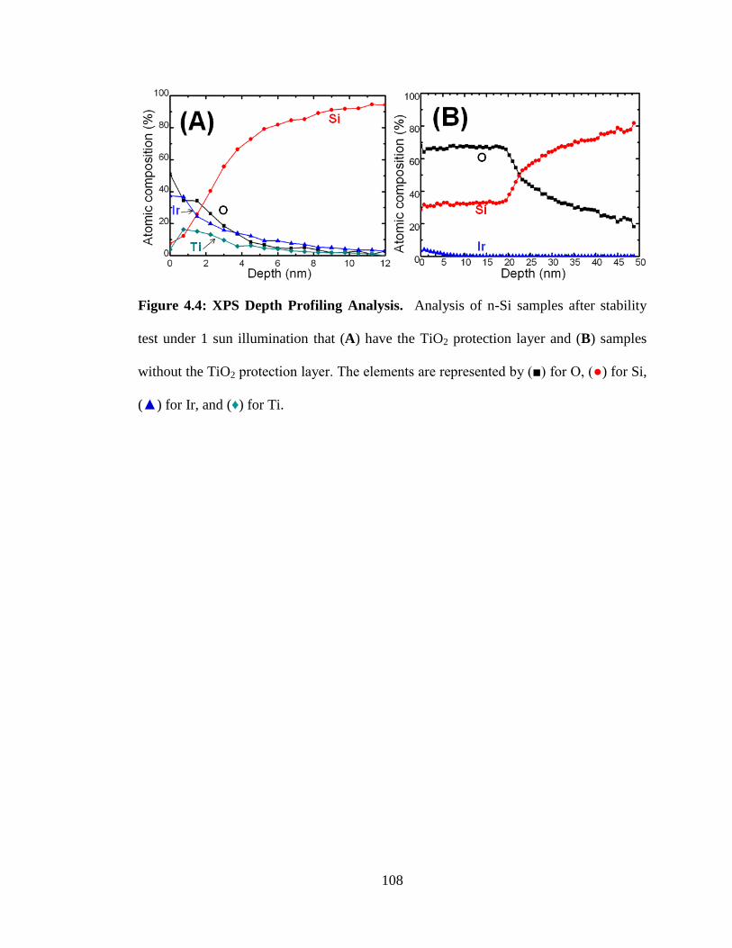
108
Figure 4.4: XPS Depth Profiling Analysis. Analysis of n-Si samples after stability
test under 1 sun illumination that (A) have the TiO2 protection layer and (B) samples
without the TiO2 protection layer. The elements are represented by () for O, () for Si,
() for Ir, and (♦) for Ti.
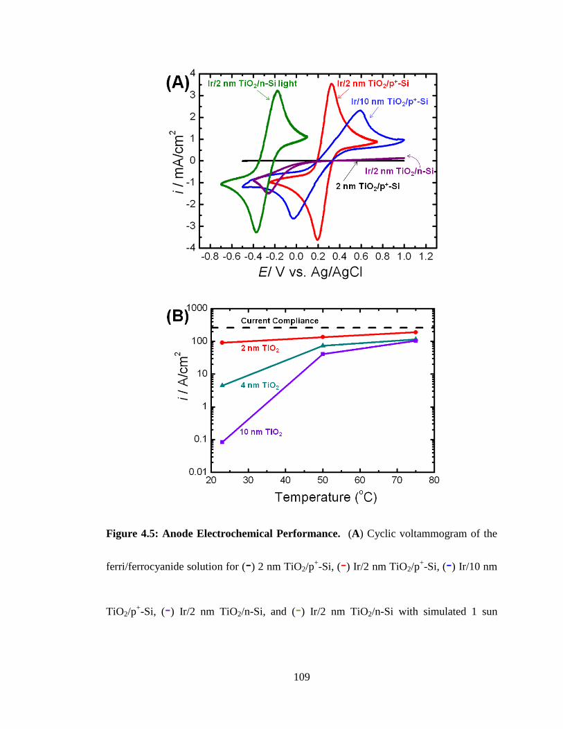
109
Figure 4.5: Anode Electrochemical Performance. (A) Cyclic voltammogram of the
ferri/ferrocyanide solution for (-) 2 nm TiO2/p+-Si, (-) Ir/2 nm TiO2/p
+-Si, (-) Ir/10 nm
TiO2/p+-Si, (-) Ir/2 nm TiO2/n-Si, and (-) Ir/2 nm TiO2/n-Si with simulated 1 sun

110
illumination. All measurements were done in the dark except otherwise mentioned. (B)
Temperature dependent current density measurement through () 2 nm, () 4 nm, and
() 10 nm TiO2 films on p+-Si substrates. The line (-) indicates the compliance of the
meter. 50 nm thick Ir dots of 100 m diameter were used as the top metal contact.
Current measured in a probe station (no electrolyte present) at a Si substrate voltage vs.
the Ir contact of 0.5 V (flatband voltage=-0.13 V). Current-voltage data are provided in
the supplementary materials (section 4.9).

111
Table 4.1: Water oxidation overpotentials measured at 1 mA/cm2.
Substrate 1M NaOHa (V) pH 7
a (V) 1M H2SO4
a (V)
Ir/TiO2/p+-Si (Dark)
0.384 0.346 0.332
Ir/TiO2/n-Si (Light)
-0.171 -0.219 -0.200
a Calculated E
0 values of 1M NaOH, pH 7 and 1M H2SO4 solutions are +0.417 V,
+0.816 V, +1.206 V vs. NHE respectively.

112
4.8: References
1. Lewis, N. S. & Nocera, D. G. Powering the planet: Chemical challenges in solar
energy utilization. Proc. Natl. Acad. Sci. 103, 15729-15735, (2006).
2. Lewis, N. S. Toward cost-effective solar energy use. Science 315, 798-801,
(2007).
3. Pourbaix, M. J. N. Atlas of electrochemical equilibria in aqueous solutions. 1st
Edi., (Pergamon Press, 1966).
4. Hwang, Y. J., Boukai, A. & Yang, P. D. High Density n-Si/n-TiO2 Core/Shell
Nanowire Arrays with Enhanced Photoactivity. Nano Lett. 9, 410-415, (2009).
5. Walter, M. G. et al. Solar Water Splitting Cells. Chem. Rev. 110, 6446-6473,
(2010).
6. Kay, A., Cesar, I. & Gratzel, M. New benchmark for water photooxidation by
nanostructured alpha-Fe2O3 films. J. Am. Chem. Soc. 128, 15714-15721, (2006).
7. Sivula, K., Le Formal, F. & Gratzel, M. WO3-Fe2O3 Photoanodes for Water
Splitting: A Host Scaffold, Guest Absorber Approach. Chem. Mater. 21, 2862-
2867, (2009).
8. Matsumura, M. & Morrison, S. R. Anodic Properties of N-Si and N-Ge
Electrodes in HF Solution under Illumination and in the Dark. J. Electroanal.
Chem. 147, 157-166, (1983).

113
9. Fan, F. R. F., Keil, R. G. & Bard, A. J. Semiconductor Electrodes .48. Photo-
Oxidation of Halides and Water on N-Silicon Protected with Silicide Layers. J.
Am. Chem. Soc. 105, 220-224, (1983).
10. Howe, A. T., Hawkins, R. T. & Fleisch, T. H. Photoelectrochemical Cells of the
Electrolyte-Metal-Insulator-Semiconductor (Emis) Configuration .1. Metal
Thickness and Coverage Effects in the Pt-Silicon Oxide-N-Si System. J.
Electrochem. Soc. 133, 1369-1375, (1986).
11. Contractor, A. Q. & Bockris, J. O. M. Investigation of a Protective Conducting
Silica Film on N-Silicon. Electrochim. Acta 29, 1427-1434, (1984).
12. Kohl, P. A., Frank, S. N. & Bard, A. J. Semiconductor Electrodes .11. Behavior
of N-Type and P-Type Single-Crystal Semiconductors Covered with Thin
Normal-TiO2 Films. J. Electrochem. Soc. 124, 225-229, (1977).
13. Suleymanov, A. S. On the possibility of the transformation of solar energy to
chemical energy in the electrochemical cell with photoanode CdSe/TiO2. 16,
741-743, (1991).
14. Siripala, W., Ivanovskaya, A., Jaramillo, T. F., Baeck, S. H. & McFarland, E.
W. A CU2O/TiO2 heterojunction thin film cathode for photoelectrocatalysis.
Sol. Energ. Mat. Sol. C 77, 229-237, (2003).
15. Rajeshwar, K., Kaneko, M., Yamada, A. & Noufi, R. N. Photoelectrochemical
Oxidation of Halide-Ions at Naked, Catalytically Modified, and Polymer-Coated
N-Cds Electrodes in Aqueous-Media. J. Phys. Chem. 89, 806-811, (1985).

114
16. Ritala, M. & Leskela, M. Atomic layer epitaxy - a valuable tool for
nanotechnology? Nanotechnology 10, 19-24, (1999).
17. Liu, F. et al. Mechanisms of water oxidation from the blue dimer to photosystem
II. Inorg. Chem. 47, 1727-1752, (2008).
18. Kanan, M. W. & Nocera, D. G. In situ formation of an oxygen-evolving catalyst
in neutral water containing phosphate and Co2+
. Science 321, 1072-1075,
(2008).
19. Yagi, M., Tomita, E., Sakita, S., Kuwabara, T. & Nagai, K. Self-assembly of
active IrO2 colloid catalyst on an ITO electrode for efficient electrochemical
water oxidation. J. Phys. Chem. B 109, 21489-21491, (2005).
20. Comninellis, C. & Vercesi, G. P. Characterization of DSA-Type Oxygen
Evolving Electrodes - Choice of a Coating. J. Appl. Electrochem. 21, 335-345,
(1991).
21. Nakagawa, T., Bjorge, N. S. & Murray, R. W. Electrogenerated IrOx
Nanoparticles as Dissolved Redox Catalysts for Water Oxidation. J. Am. Chem.
Soc. 131, 15578-15579, (2009).
22. ERDA/NASA -1022/77/16, (1977).
23. Fujishima, A. & Honda, K. Electrochemical Photolysis of Water at a
Semiconductor Electrode. Nature 238, 37-38, (1972).

115
24. Howe, A. T. & Fleisch, T. H. Photoelectrochemical Cells of the Electrolyte-
Metal-Insulator-Semiconductor (Emis) Configuration .2. Use of Nonnative
Oxides in Pt/Oxide/N-Si Systems. J. Electrochem. Soc. 134, 72-76, (1987).
25. Process Integration, Devices, and Structures. International Technology
Roadmap for Semiconductors,
<http://www.itrs.net/links/2008ITRS/Update/2008Tables_FOCUS_A.xls>
(2008).
26. Ouattara, L. et al. Dimensionally stable anode-type anode based on conductive
p-silicon substrate. J. Electrochem. Soc. 150, D41-D45, (2003).
27. Switzer, J. A. The N-Silicon Thallium(III) Oxide Heterojunction
Photoelectrochemical Solar-Cell. J. Electrochem. Soc. 133, 722-728, (1986).
28. Green, M. A., Emery, K., Hishikawa, Y. & Warta, W. Solar cell efficiency
tables (version 35). Prog. Photovoltaics 18, 144-150, (2010).
29. Nozik, A. J. P-N Photoelectrolysis Cells. Appl. Phys. Lett. 29, 150-153, (1976).
30. Nelson, J. The physics of solar cells. (Imperial College Press, 2003).
31. Sharpe, A. G. The chemistry of cyano complexes of the transition metals.
(Academic Press, 1976).
32. Schuegraf, K. F. & Hu, C. M. Hole Injection SiO2 Breakdown Model for Very-
Low Voltage Lifetime Extrapolation. IEEE Trans. Electron. Dev. 41, 761-767,
(1994).

116
33. Nelson, J. & Chandler, R. E. Random walk models of charge transfer and
transport in dye sensitized systems. Coord. Chem. Rev. 248, 1181-1194, (2004).
34. Doering, R. & Nishi, Y. in Handbook of Semiconductor Manurfacturing
Technology 14-11 – 14-37 (CRC Press, Boca Raton, 2008).
35. Raaijmakers, I., Soininen, P. T., Granneman, E. H. A. & Haukka, S. P.
Protective Layers prior to Alternating Layer Deposition. USA patent US
2001/0054769A1 (2001).

117
4.9: Supporting Materials
Materials. All chemicals used in this study were purchased from commercial
sources and used as received. Degenerately doped p+-type Si (100) wafers (0.001-0.002
Ωcm, 500 m thickness) and n-type Si (100) wafers (0.1-0.2 Ωcm, 500 m thickness)
were purchased from El-Cat. All electrochemical measurements were performed in
electrolyte solutions prepared with DI water. A ferri/ferrocyanide solution was made to
be 10 mM of both K3Fe(CN)6 and K4Fe(CN)6∙3H2O in 1 M aqueous KCl. Experiments
for water electrolysis were performed in either acidic (1 M H2SO4), neutral (1 M
phosphate-buffered, pH 7) or basic (1 M NaOH) solutions.
Sample Preparation. Atomic layer deposition (ALD) of TiO2 was performed at
200°C on silicon wafers that were coated with a thin (< 2 nm) chemical oxide as a result
of surface preparation by the wafer vendor. Tetrakisdmethylamido titanium (TDMAT)
was used as the titanium source and water vapor as oxygen source. Each source was
heated to a line temperature of 80°C. The system pressure was maintained at 1.1 Torr
nominally, and nitrogen was used as the carrier gas. The pulse and purge durations of
the titanium and water sources were 5 s and 0.75 s respectively. Unless stated
otherwise, a total of 24 cycles of ALD was performed to obtain a TiO2 film of
approximately 2 nm thickness. The noble metal layer was then deposited by e-beam
evaporation with a quartz crystal balance used to monitor the thickness of material
deposited to obtain the nanocomposite electrode. For all samples, a thin layer (3 nm) of
metal was e-beam evaporated onto the backside of the silicon wafer (platinum for p+-Si
samples and aluminum for n-Si samples). This backside metal forms the electrical
contact and eliminates any Schottky junctions that could be formed at the back of the

118
substrate. Samples were annealed in forming gas (95% N2, 5% H2) at 400°C for 30
minutes in a quartz tube furnace before experiments were performed.
Electronic tunneling mediated by the metallic overlayer. Efficient direct
tunneling from the Si substrate through a thin TiO2 layer requires sufficient density of
states in the layer above TiO2. A metal layer (e.g. Pt, Ir, Ru, etc…) has abundant density
of states, and therefore, could sustain large tunneling current. The liquid electrolytes,
however, have limited density of states, resulting in the low tunneling current when they
are in direct contact with TiO2. Therefore, the metal layer effectively mediates the
charge transfer from Si and the reaction with the electrolyte. Other conductive catalysts,
such as IrO2, are also capable of serving the same role as the demonstrated metal
catalyst layers, with details to be reported in future publications.
Electrochemical Methods. All electrochemical experiments were performed
on either a WaveNow or WaveNano potentiostat (Pine Research Instrumentation) in air
at room temperature. A Pt wire was used as the counter electrode and a glass frit-
isolated Ag/AgCl/sat. KCl electrode as the reference electrode. A 5 mm bored Teflon
cone (area 0.196 cm2) was pressed against the DI water-rinsed nanocomposite working
electrode. All measured potentials were converted to the NHE reference scale using
E(NHE) = E(Ag/AgCl/KCl) + 0.197 V. The pH values for the electrolyte solutions used
in this study were determined by utilizing a reversible hydrogen electrode and
measuring the open circuit potential for each solution and adjusting the pH dependent
water oxidation potentials accordingly. Hydrogen gas was sparged into the electrolyte
solutions for ten minutes, with a platinum rotating disc electrode as the working
electrode and platinum mesh as the counter electrode.

119
Cyclic voltammetry (CV). All CVs were measured, unless stated otherwise, at
100 mV/s in the indicated electrolyte solution. The open circuit potential (OCP) was
measured before each experiment and used as the starting and ending potential for each
CV. A peristaltic pump (Cole Parmer, Norprene tubing, ID = 1.6 mm) was used to
continuously circulate electrolyte solution at a flow rate of 1 mL/s impinging on the
sample in the bore of the Teflon cone for all dark and illuminated water electrolysis
experiments (Figure 4.S1 for dark, Figure 4.S2 for illuminated). CV’s obtained with
solar illumination on n-Si anodes were performed in static solutions without pumping.
A modified pumping configuration with the electrolyte flow entering through an angled
hole in the side of the bore of the Teflon cone was used for stability tests conducted
under solar illumination so as not to block the light with the delivery tube (Figure 4.S2).
Table S1 lists the peak-to-peak splitting for the ferri/ferrocyanide solution for different
anode structures.
Impedance spectroscopy measurements. Impedance spectroscopy was
performed on a Princeton Applied Science impedance spectrometer to determine the
solution resistance of the electrolytes used in this study. The Nyquist plots for the
acidic, neutral and basic electrolyte solutions are shown in Figure 4.S3. Extrapolation
of the Nyquist plots to large frequencies reveals series resistance to be 7.5 Ω, 33.5 Ω
and 15 Ω for the acidic, neutral and basic solutions respectively. The obtained series
resistance values correspond to theoretical calculations very well. As an example, the
resistivity of 1 M NaOH is 5.9 cm (by linear extrapolation). By using a cylindrical
geometry of 5 mm height and 5 mm diameter, the calculated resistance is 15 .
120
Chronoamperometry. Chronoamperometry experiments were performed by
holding the potential at 1.5 V vs. Ag/AgCl/KCl reference electrode and monitoring the
current over time in 10 mL of the specified electrolyte solution. The electrolyte
solution was circulated with the peristaltic pump as described above. Results for a 18
hour experiment in neutral solution without illumination are shown in Figure 4.S4
below.
Chronopotentiometry (CP). All CP experiments were performed by holding
the current constant at 1 mA across a 0.196 cm2 anode surface area while monitoring
the potential over time in 10 mL of the specified electrolyte solution. The electrolyte
solution was circulated with the peristaltic pump using the procedure described above.
Diffusion-limited current. To understand the discrepancy between the
expected current density values obtained by extrapolation of the measured Tafel slopes
at low current density and the measured values obtained during CP and CA
experiments, diffusion-limited currents were estimated by determining the limiting
current for ferrocyanide oxidation under identical flow conditions and then adjusting
that value for the concentrations and the published diffusion constants of the different
species that might limit mass transfer during water oxidation: either transport of the
reactants (H2O or OH-) to the surface or transport of the products (O2 and H
+ or H2O)
away from the surface. The analysis showed that with a flow rate of 1 mL/s, mass
transfer of the reactants to the surface should not be limiting, with achievable current
densities beyond the solar flux limitations at 1 sun illumination. However, a major
discrepancy was found for mass transport of the sparingly soluble product of water
oxidation, O2, away from the electrode surface. Under the fastest flow rates possible in

121
our cell, 2 mL/s, oxygen bubbles would be expected to form at current densities of a
few mA/cm2. Because the current distribution is not expected to be uniform when mass
transport is limiting in this flow arrangement, we expect that bubbles form when the
average current density is of the order 1 mA/cm2. These bubbles should effectively
decrease the catalytic surface area and thus reduce the total current at a specific
overpotential relative to that expected by extrapolation of the Tafel slope measured at
low current density.
Temperature dependent tunneling experiments. Temperature dependent
tunneling experiments were performed on Ir/TiO2/p+-Si electrodes. Three thicknesses (2
nm, 4 nm, and 10 nm) of TiO2 were chosen to observe the thickness-dependent
tunneling behavior. A shadow mask is used to define the circular top metal contacts of
100 m diameter. The thickness of Ir top metal contact is 50 nm. The substrate bias was
scanned from 0 to 1 V while monitoring the current density, as shown in Figure 4.S5.
Transmission electron microscopy of Ir/TiO2/p+-Si anode after stability test.
Cross-sectional TEM was conducted after the 3 hr CP stability test (constant current at 5
mA/cm2) for the Ir/TiO2/p
+-Si sample (Figure S6). Comparing Figure 4.S6 with Figure
4.1B, it is evident that cross-sectional TEM images detect no apparent structural change
in the TiO2-protected anodes after the life test.
X-ray photoelectron spectroscopy (XPS). The XPS measurements were
performed using a PHI VersaProbe system with a 100 W Al-Kα X-ray source on a spot
size of 100 µm at a 45° incident angle. The binding energy scan range was 0-1200 eV
in 1 eV steps, and the pass energy was 117.4 eV, which provides the optimal balance

122
between scan resolution and counting statistics in our system. A dual beam neutralizer
(7 V Ar+ and 30 V electron beam) was used to neutralize sample charging. XPS depth
profiling was performed using an Ar+ ion beam at 2 kV and 1 A with an area of 2x2
cm. Spectra were collected at intervals of 3 s during sputtering.
Atomic Force Microscopy (AFM). The AFM images for these samples were
taken on a Park XE-70 instrument set on a non-contact tapping mode with a scan rate of
1 Hz. A representative AFM image of the nanocomposite anode after synthesis is
shown in Figure 4.S9.

123
4.10: Supporting Materials Figures
Figure 4.S1. Cross-sectional schematic of experimental setup utilized for dark
electrochemical experiments on Ir/TiO2/p+-Si anodes.

124
Figure 4.S2. Cross-sectional schematic of experimental setup utilized for stability tests
with n-Si/TiO2/Ir under solar illumination. This geometry allows for unobstructed
illumination of the sample.

125
Figure 4.S3. Nyquist plots from series resistance measurements from (A) acidic, (B)
neutral and (C) basic solutions measured from 300 kHz to 0.1 Hz.

126
Figure 4.S4. Constant potential measurement at 1.5 V vs. Ag/AgCl/sat. KCl in pH 7
buffered solution without illumination for 18 hours for Ir/p+-Si (∙∙∙) and Ir/TiO2/p
+-Si
(-).

127
Figure 4.S5. Temperature dependent tunneling current measurement for the Ir/TiO2/p+-
Si electrode. The ALD-grown TiO2 thicknesses were (A) 2 nm, (B) 4 nm, and (C) 10

128
nm. Measurements were taken at (-) 23oC, (-) 50
oC, and (-) 75
oC. The line (-)
indicates the compliance of the meter.

129
Figure 4.S6. Cross-sectional TEM image of Ir/TiO2/p+-Si anode taken after 3 hr
constant current (5 mA on a sample area of 0.196 cm2) stability test.

130
Figure 4.S7. Equilibrium band diagrams. (A) Ir/TiO2/p+-Si and (B) Ir/TiO2/n-Si anode
in contact with ferrocyanide solution. It is assumed that the redox level of the solution
equilibrates with the Ir metal catalyst.

131
Figure 4.S8. Light saturated current density. Cyclic voltammogram of Ir/TiO2/n-Si in
1M H2SO4 under simulated solar illumination at 1 sun.

132
Figure 4.S9. AFM image of Ir covered ALD-TiO2 sample. Root-mean-square
roughness ~0.2 nm

133
Table S1. Summary of peak-to-peak potential separation for anodes measured in
ferri/ferrocyanide solution
Substrate Eanodic to Ecathodic (mV)
TiO2/Si No observable peaks
Ir/TiO2/Si
130
Indium Tin Oxidea
220
a Delta Technologies, Product # CB-40IN-S211, 4-8 Ω with a small area, front-side
electrical contact outside the Teflon cone perhaps inducing a series resistance that
accounts for the larger peak-to-peak separation.

134
Chapter 5: Effect of TiO2 Thickness and Catalyst Layer on Efficiency and
Stability of Silicon Anodes for Water Oxidation
5.1: Preface
This chapter is an extension of the work that was done in Chapter. This work
explores what effects various thicknesses of the TiO2 protective layer have on charge
transfer efficiency and stability of the catalyst/TiO2/p+-Si anode. Additionally, the
catalyst layer was changed from iridium to other metals to examine the functionality
and utility of the TiO2/p+-Si base substrate. Understanding how the catalyst layer and
protective coating thickness effects both charge transfer efficiency and stability will
enable the development of more versatile anodes to use electricity for fuel synthesis.
I collected all of the data in this chapter while Vincent Chen and Rathnait Long
helped with the anode fabrication. The results reported here are being expanded upon
and will be incorporated into a manuscript to be submitted for publication.

135
5.2: Abstract
Recently, we reported on a silicon-based photoanode structure for
photoelectrochemical water oxidation stabilized by a thin layer of titanium dioxide
grown by atomic layer deposition. The catalyst layer was chosen to be iridium due to
its efficiency in catalyzing the water oxidation reaction and relative stability in a range
of pH values. Herein, we report on silicon/titanium dioxide/catalyst structures with
various thicknesses of titanium dioxide and the effect these different thicknesses have
on overall anode efficiency and the stability during water oxidation. Additionally, the
titanium dioxide was coated with different catalyst layers in order to study the
versatility of the anode for supporting these catalysts as well as the performance of each
layer for the oxidation of water.

136
5.3: Introduction
Electrochemical water splitting has long been considered a promising strategy to
store renewable electricity in the form of molecular fuels.1, 2
Of the two half reactions
necessary for water splitting (Scheme 1), the water oxidation half-reaction has been
considered the kinetic bottleneck due to the large overpotentials commonly associated
with the reaction. The water reduction half reaction (E° = 0 V vs. NHE at pH 0)
produces molecular hydrogen which can be used as a fuel.
Scheme 1: Water oxidation and proton reduction half reactions and pH-dependent
reversible potentials.
In order to be considered for large scale commercial use, a photoelectrochemical
water splitting device must utilize a cheap catalyst that minimizes the overpotential and
increases the efficiency of the water-oxidation half reaction.3, 4
Recently, we have
reported on a nanocomposite photoanode protected by a thin layer of titanium dioxide
(TiO2) that was deposited by atomic layer deposition (ALD) onto a photoactive silicon
substrate. An iridium layer was used as the water oxidation catalyst.5 This structure
takes advantage of a minimal amount of precious metal catalyst in order to decrease the
overall cost of the device while minimizing the absorption of sunlight prior to its
absorption by the photoactive silicon. Here, we report on how altering the thickness of
the protecting TiO2 layer and how changing the water oxidation catalyst layer effects
the resulting charge transfer efficiency and stability of the silicon-based anode toward
water oxidation.
137
5.4: Results and Discussion
The original photoanode structure was protected with a thin, conformal TiO2
protection layer deposited by ALD that was made to be 2 nm thick. In this study, we
employ otherwise similar anodes that can function in the dark by use of heavily
phosphorous-doped silicon substrates (p+-Si, 0.001-0.005 Ω·cm, 500 μm thick) coated
with ALD-TiO2 by exposing the surface to a titanium precursor, tetrakis-
(dimethylamido)titanium (TDMAT), and water vapor in alternating cycles until
thicknesses of 2, 5 and 10 nm were obtained. After e-beam depositing 2 nm of iridium
on each of these samples, the electron transport efficiency as a function of TiO2
thickness was investigated by monitoring the Fe2+/3+
couple in a 1 M aqueous KCl
solution containing 10 mM of both K4Fe(CN)6 and K3Fe(CN)6 (FFC solution) using
cyclic voltammetry (CV). The results in Figure 5.1A show that an increasing TiO2
thickness increases the peak-to-peak splitting of the oxidation and reduction peaks and
decreases the overall current density obtained. This effect is more dramatic with the
sample having a 10 nm TiO2 coating, indicating charge transfer efficiency through the
structure decreases rapidly as a function of increasing TiO2 thickness.
The peak-to-peak splitting values are plotted as a function of TiO2 thickness in
Figure 5.1B. These results show an exponential-type relationship which indicates that
charge transport through the structure occurs via a tunneling mechanism. This result is
not unexpected as current densities of up to a few A/cm2 are known to occur through
ultrathin oxide layers deposited by ALD in state-of-the-art field effect transistors.6 We
believe this conduction occurs by tunneling through the TiO2. The layer was previously
found to be uniform and continuous by TEM with no evidence of the catalyst layer

138
intercalating into the TiO2 layer to provide an alternative mechanism to transfer charge
through the insulating oxide layers of the anode. To date, ALD is the only method
capable of depositing such thin conformal layers free of any pinholes or cracks that
would otherwise allow for metal intercalation or oxidation of the underlying silicon
substrate by the electrolyte.7, 8
The charge transfer efficiency through the anodes with different TiO2
thicknesses can be further demonstrated by performing water oxidation. Figure 5.1C
shows water oxidation CVs that were performed in a 1 M NaOH solution.9 The
samples with thicker TiO2 layers had decreased performance for water oxidation when
compared to samples with thinner TiO2 layers. Figure 5.1D shows the water oxidation
overpotentials for each TiO2 thickness required to obtain a current density of 1 mA/cm2.
The current density obtained at any applied electrochemical potential decreases as the
thickness of the TiO2 protective coating is increased, consistent with the increasing
peak-to-peak splitting results obtained for the FFC solution shown in Figure 5.1B. The
maximum current density obtained at a given applied electrochemical potential was
observed to decrease as the TiO2 thickness was increased. The TiO2 layer can be
viewed as a resistor, where an increasing TiO2 thickness increases the series resistance
through which the current flows. This increasing resistance will decrease the current
density at a given overpotential, and thus the efficiency, that can be obtained by the
anode.
Once the charge transfer behavior was established, the stability of the interface
toward water oxidation was investigated as a function of the TiO2 thickness. Each
sample was subjected to a constant potential endurance test by holding the

139
electrochemical potential at 1.65 V vs. NHE in a 1 M H2SO4 solution for up to 48 hours
(Figure 5.2A). This applied electrochemical potential corresponds to a 444 mV
overpotential at this pH, which represents a value at which most water oxidation
catalysts of interest could operate at reasonable current density (see Table 5.1). CVs of
water oxidation in 1 M H2SO4 solution were performed before the stability test for each
sample (Figure 5.2B). The current density at the beginning of the stability test was
observed to be comparable to the current density obtained at the same overpotential in
these CVs. The current density initially decreases to reach a steady-state current for
samples that have TiO2 protective coatings. This diffusion-limited current density of 1-
2 mA/cm2 is due to the inefficient removal of molecular oxygen bubbles away from the
anode surface (see supporting materials). The samples containing the TiO2 protective
coating were found to remain operational throughout the entirety of the stability test of
48 hours in this report. The sample without the TiO2 layer was found to decrease to a
current density below that of the sample with 5 nm of TiO2 within half an hour and
decrease steadily to a minimal value after 25 hours. XPS analysis of this sample after it
was stopped reveals a loss of Ir and increase in Si peaks attributed to SiO2 (Figure 5.3A)
The loss of Ir from the surface is most likely due to either oxidative stress or poor
adhesion of the Ir layer to TiO2 with each removal mechanism accelerated by pumping
the electrolyte solution. Ir loss was also observed for samples with the TiO2 protective
coating, indicating the failure mechanism is due to SiO2 growth, which is consistent
with previously published results.5 It is worth noting that the current densities
obtained for the 10 nm TiO2 sample are consistent with the model of thicker TiO2 layers
having more resistance and less measured current density. This observation highlights

140
the importance of balancing stability with efficiency for these anodes to be considered
for commercial, large scale use. Currently, new photoelectrochemical water splitting
flow cell devices are being designed that will more efficiently remove oxygen bubbles
from the anode while allowing for light absorption.
The thickness of the Ir catalyst layer on top of the TiO2/p+-Si anode was also
varied in order to determine how this affected the anode charge transfer efficiency. The
thickness of the Ir layer from the standard 2 nm was changed to smaller and larger
thicknesses of 1 nm and 3 nm, each deposited onto samples with 2 nm of TiO2. The Ir
layer thickness was found to have a negligible effect on the FFC peak-to-peak splitting
and water oxidation in acidic (1 M H2SO4), neutral (1 M phosphate-buffered) and basic
(1 M NaOH) solutions (Table 5.1). This result indicates that thinner Ir layers could be
employed in photoelectrochemical water splitting devices as efficiency would not suffer
and the amount of precious metal catalyst, and thus cost, would be minimized. The
catalyst layer is vital, however, as no charge will pass without the layer present to act as
a tunnel mediator between the silicon base substrate and redox species in solution. It
has yet to be determined how the catalyst thickness will be affected by the loss of Ir
observed during stability tests.
In addition to varying the thickness of the Ir catalyst, the type of catalyst was
also varied. Different catalysts may be optimal for different electrochemical reactions.
These catalyst layers were deposited onto TiO2/p+-Si anodes with a 2 nm TiO2 layer.
The results of these studies are tabulated in Table 5.1. A 3 nm layer of ruthenium was
found to be a competent water oxidation catalyst in the acidic solution. The active form
of the catalyst was likely a ruthenium oxide formed in situ as evidenced by a pre-

141
oxidation peak near the onset of the water oxidation wave (see supporting materials).
The overpotentials required to obtain 1 mA/cm2 were comparable to the Ir catalyst in
the acidic solution, but the catalyst dissolved off the anode with successive CV scans
and increasing pH. A 2 nm layer of platinum was also deposited and found to have
comparable charge transfer efficiency in FFC but displayed larger overpotentials for
water oxidation at all pH values. This is due to the fact Pt is not as good as a water
oxidation catalyst as Ir or Ru.10-13
Despite the inefficiency at catalyzing water
oxidation, the Pt layer still demonstrates the comparable ability to mediate charge
transfer to and from the silicon substrate as evidenced by the FFC peak-to-peak splitting
results. A 2 nm gold layer deposited onto the anode structure was found to have a peak-
to-peak splitting value of 120 mV in the FFC solution which was as efficient as the 3
nm of Ir catalytic layer. The water oxidation behavior of the gold layer resulted in large
overpotentials, consistent with the fact that gold is not a good water oxidation catalyst.
A 2 nm Co catalyst layer was also deposited and found to have large peak-to-peak
splitting in the FFC solution. This result indicates that the Co layer is not a good
electron transfer mediator possibly due to poor adhesion of the layer to the TiO2.
The search for a cheap, efficient and robust water oxidation catalyst made from
earth-abundant elements has led to the discovery of a cobalt-phosphate (Co-Pi) catalyst
found to oxidize water in neutral pH.14
Although the oxidized form of cobalt, Co3O4, is
known to oxidize water15
, the observed overpotentials for the planar Co layer were
found to be considerably greater than the Ir and Ru catalyst layers observed in this
report. To improve on the water oxidation overpotentials, the Co-Pi catalyst was
deposited in situ following published procedures.14
The deposited Co-Pi catalyst did

142
decrease the overpotential by 236 mV for water oxidation in the pH 7 solution but had a
minor effect in the acidic and basic solutions. Furthermore, the overpotential necessary
to obtain a current density of 1 mA/cm2 was found to be 400 mV worse than the Ir and
Ru catalyst layers at pH 7. This result is consistent with the thin layer of Co deposited
exhibiting poor electron transfer efficiency with the FFC solution. The Co-Pi catalyst
deposited here does not compare well to the results of the original study14
which reports
an overpotential of around 400 mV for 1 mA/cm2 at pH 7, not 730 mV as obtained here.
It is worth noting, however, that in this work the catalyst was deposited onto a Co layer
instead of an indium tin-doped oxide (ITO) electrode as was originally published. A
recent report has illustrated the ability to deposit the CoPi catalyst onto a thin layer of
ITO that was coating a pn junction Si wafer to be used for photoelectrochemical water
splitting.16

143
5.5: Conclusions
This report has highlighted the effect that changing the TiO2 thickness of the
nanocomposite catalyst/TiO2/p+-Si anode has on charge transport behavior and water
oxidation efficiency. The charge transport efficiency through the structure decreases as
the TiO2 thickness is increased. This is consistent with the model of the TiO2 layer
acting as a resistor in series with the electrochemical process and charge transfer though
the structure. The catalyst layer on the TiO2 was also varied in order to study the effect
different metal layers have on electron transfer and water oxidation in a range of pH
solutions. The Ir layer was found to be the best performing at all pH values overall, but
other catalyst layers have been shown to be capable catalyst layers that may allow for
greater functionality of the anode for other electrochemical reactions.

144
5.6: Figures
Figure 5.1: Electrochemical Results of Anodes with Various TiO2 Thicknesses. (A)
CVs in the FFC solution using 2 nm of Ir deposited onto various thicknesses of TiO2 on
p-Si anodes. (B) Plot of peak-to-peak splitting values in panel (A) as a function of TiO2
thickness. (C) Water oxidation CVs in 1 M NaOH solution using 2 nm of Ir deposited
onto various thicknesses of TiO2 on p-Si anodes. (D) Calculated overpotentials for the
samples in panel (C) to obtain a current density of 1 mA/cm2. The pH value for the 1 M
NaOH solution was found to be 13.7 as measured against the reversible hydrogen
electrode leading to a reversible potential of 0.418 V versus NHE. The corrected
solution resistance was 15 Ω as measured by electrochemical impedance spectroscopy.
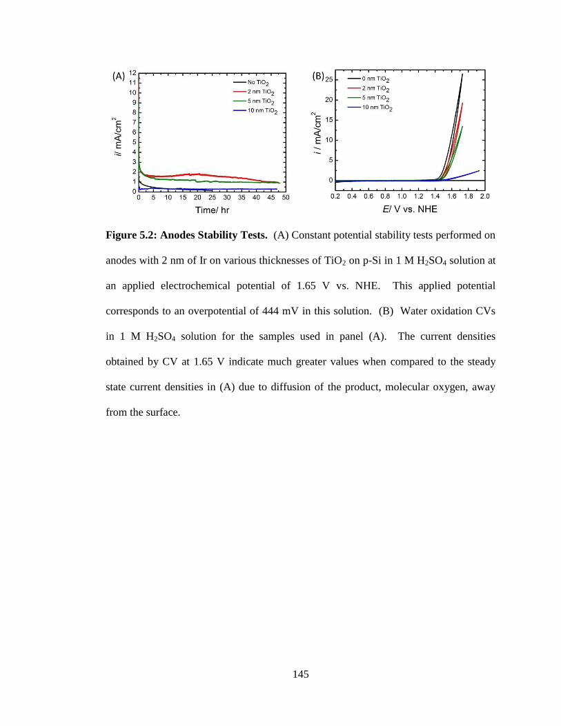
145
Figure 5.2: Anodes Stability Tests. (A) Constant potential stability tests performed on
anodes with 2 nm of Ir on various thicknesses of TiO2 on p-Si in 1 M H2SO4 solution at
an applied electrochemical potential of 1.65 V vs. NHE. This applied potential
corresponds to an overpotential of 444 mV in this solution. (B) Water oxidation CVs
in 1 M H2SO4 solution for the samples used in panel (A). The current densities
obtained by CV at 1.65 V indicate much greater values when compared to the steady
state current densities in (A) due to diffusion of the product, molecular oxygen, away
from the surface.

146
Figure 5.3: XPS Analysis of Samples Before and After Stability Tests. (A) X-ray
photoelectron (XPS) spectra of Ir, Si and Ti regions for a 2 nm Ir layer deposited onto a
p-Si substrate before () and after () the stability test in 1 M H2SO4 solution. The
binding energy for atomic Si in the bulk is at 100 eV, while the binding energy for Si in
SiO2 is 104 eV, both shown to be increasing after the stability test was performed. This
sample lost Ir as the stability test was conducted and is absent of Ti. (B) XPS spectra
for Ir, Si and Ti regions for 2 nm Ir layer deposited onto the 5 nm TiO2/p-Si substrate
before () and after () the stability test in 1 M H2SO4 solution. This sample was
operational after the stability test, indicating that the loss of Ir is not the reason for
failure of the sample without the TiO2 layer. The Ti peak is shown to increase, while
the underlying Si was not observed.

147
Table 5.1. Results obtained for peak-to-peak splitting of ferro/ferri cyanide (FFC)
peaks and water oxidation overpotentials at 1 mA cm-2
for different catalyst layers on
2 nm of TiO2 on p+-Si.
Catalyst layer FFC splitting (mV) 1 M Acid (mV) 1 M Neutral (mV) 1 M Base (mV)
1 nm Ir 160 300 311 340
2 nm Ir 140 282 319 337
3 nm Ir 120 265 316 343
3 nm Rua 195 265 383 -
2 nm Pt 175 469 628 575
2 nm Aub 120 1160 1120 790
2 nm Co > 1000 885 966 937
2 nm Co + CoPic > 1000 817 730 1061
a Catalyst layer found to dissolve off electrode with increasing cycle numbers and pH
b Deposited onto 1 nm Ti adhesion layer on TiO2/p
+-Si
c Co-Pi catalyst deposited according to published procedures
14

148
5.7: References
1. Lewis, N. S., Powering the planet. MRS Bull. 2007, 32, (10), 808-820.
2. Walter, M. G.; Warren, E. L.; McKone, J. R.; Boettcher, S. W.; Mi, Q.; Santori,
E. A.; Lewis, N. S., Solar Water Splitting Cells. Chem. Rev. 2010, 110, (11),
6446-6473.
3. Gratzel, M., Photoelectrochemical cells. Nature 2001, 414, (6861), 338-344.
4. Brimblecombe, R.; Dismukes, G. C.; Swiegers, G. F.; Spiccia, L., Molecular
water-oxidation catalysts for photoelectrochemical cells. Dalton Trans. 2009,
(43), 9374-9384.
5. Chen, Y. W.; Prange, J. D.; Duehnen, S.; Park, Y.; Gunji, M.; Chidsey, C. E. D.;
McIntyre, P. C., Atomic layer-deposited tunnel oxide stabilizes silicon
photoanodes for water oxidation. Nature Mat. 2011, 10, 539-544.
6. Process Integration, Devices, and Structures. International Technology Roadmap
for Semiconductors.
http://www.itrs.net/links/2008ITRS/Update/2008Tables_FOCUS_A.xls
7. Decker, F.; Fracastorodecker, M.; Badawy, W.; Doblhofer, K.; Gerischer, H.,
The Photocurrent Voltage Characteristics of the Heterojunction Combination n-
Si/SnO2/Redox Electrolyte. J. Electrochem. Soc. 1983, 130, (11), 2173-2179.
8. Kohl, P. A.; Frank, S. N.; Bard, A. J., Semiconductor Electrodes. 11. Behavior
of n-Type and p-Type Single Crystal Semiconductors Covered with Thin
Normal TiO2 Films. J. Electrochem. Soc. 1977, 124, (2), 225-229.
9. The pH value for each of the 1 M H2SO4, 1 M phosphate buffered and 1 M
NaOH solutions were obtained by measuring the reversible hydrogen electrode

149
values in each solution. Hydrogen was sparged into the electrochemical cell and
a Pt disc was used as the working electrode with a Pt mesh as the counter
electrode. The values obtained show a pH of 0.4, 6.99 and 13.97 for the acidic,
neutral and basic solutions, respectively.
10. Yagi, M.; Tomita, E.; Kuwabara, T., Remarkably high activity of
electrodeposited IrO2 film for electrocatalytic water oxidation. J. Electroanal.
Chem. 2005, 579, (1), 83-88.
11. Nakagawa, T.; Beasley, C. A.; Murray, R. W., Efficient Electro-Oxidation of
Water near Its Reversible Potential by a Mesoporous IrOx Nanoparticle Film. J.
Phys. Chem. C 2009, 113, (30), 12958-12961.
12. Neumannspallart, M.; Kalyanasundaram, K.; Gratzel, C.; Gratzel, M.,
Ruthenium Dioxide Electrodes as Suitable Anodes for Water Photolysis. Helv.
Chim. Acta. 1980, 63, (5), 1111-1118.
13. Miles, M. H.; Klaus, E. A.; Gunn, B. P.; Locker, J. R.; Serafin, W. E., Oxygen
Evolution Reaction on Platinum, Iridium, Ruthenium and their Alloys at 80
Degrees C in Acid Solutions. Electrochimica Acta 1978, 23, (6), 521-526.
14. Kanan, M. W.; Nocera, D. G., In situ formation of an oxygen-evolving catalyst
in neutral water containing phosphate and Co2+
. Science 2008, 321, (5892),
1072-1075.
15. Iwakura, C.; Honji, A.; Tamura, H., The Anodic Evolution of Oxygen on Co3O4
Film Electrodes in Alkaline Solutions. Electrochimica Acta 1981, 26, (9), 1319-
1326.

150
16. Pijpers, J. J. H.; Winkler, M. T.; Surendranath, Y.; Buonassisi, T.; Nocera, D.
G., Light-induced water oxidation at silicon electrodes functionalized with a
cobalt oxygen-evolving catalyst. Proc. Nat. Acad. Sci., 2011, 108, (25) 10056-
10061.

151
5.8: Supporting Materials
Materials. All chemicals used in this study were purchased from commercial
sources and used as received without further purification. The Si wafers used were
degenerately doped p-type Si (100) wafers (p-Si, 0.001-0.002 Ωcm, 500 m thickness)
obtained from El-Cat. The wafers were used as received, with a thin (< 2 nm) SiO2
layer as prepared by the wafer vendor. Metal deposition was performed by e-beam
evaporation of all the catalyst layers used in this study, with the Co-Pi system deposited
according to published methods.1 The backside contact for the p-Si substrates was 2 nm
of Pt deposited by e-beam evaporation which was used to avoid any Schottky Junctions
that might form. After fabrication, the samples were heated to 400°C for 30 minutes in
a forming gas environment (95% N2, 5% H2). The electrolyte solutions were made by
dissolving the appropriate reagent into Millipore filtered water (10 MΩ resistance)
obtained on a Millipore filtration system. A ferri/ferrocyanide solution was made to be
10 mM of both K3Fe(CN)6 and K4Fe(CN)6∙3H2O in 1 M aqueous KCl. Experiments for
water electrolysis were performed in either acidic (1 M H2SO4), neutral (1 M
phosphate-buffered, pH 7) or basic (1 M NaOH) solutions. The pH of the neutral
solution was made by dissolving Na2HPO4 and NaH2PO4 in water with the pH adjusted
until a pH of 7 was achieved. All pH values were calculated by measuring the
reversible hydrogen potential in each solution and all solution resistance measurements
obtained by electrochemical impedance spectroscopy.
Sample Preparation. Atomic layer deposition (ALD) of TiO2 was performed
at 200°C on silicon wafers that were coated with a thin (< 2 nm) chemical oxide as a
result of surface preparation by the wafer vendor. Nitrogen gas was the carrier gas and
152
tetrakis-(dimethylamido)titanium (TDMAT) was used as the titanium source and water
vapor as the oxygen source. Each reagent was heated to a line temperature of 80°C
with the system pressure maintained at 1.1 Torr. The pulse and purge durations of the
titanium and water sources were 5 s and 0.75 s respectively. A total of 24 cycles of
ALD was performed to obtain a TiO2 film of approximately 2 nm thickness while 48
cycles and 120 cycles of ALD were performed to obtain TiO2 thicknesses of 5 and 10
nm, respectively. The thicknesses were obtained using ellipsometry that was calibrated
with thicknesses measured by transmission electron microscopy (TEM). The noble
metal layers were deposited by e-beam evaporation with a quartz crystal balance used to
monitor the thickness of material deposited to obtain the final anode. All samples were
annealed in forming gas (95% N2, 5% H2) at 400°C for 30 minutes in a quartz tube
furnace before experiments were performed.
Electrochemical Methods. All electrochemical experiments were performed on a
WaveNow potentiostat (Pine Research Instrumentation) in air at room temperature. A
Pt wire was used as the counter electrode and a glass frit-isolated Ag/AgCl/sat. KCl
electrode as the reference electrode. A 5 mm bored Teflon cone (area 0.196 cm2) was
pressed against the catalyst/TiO2/p-Si sample that was used as the working electrode.
The pH values for the electrolyte solutions used in this study were determined by
utilizing a reversible hydrogen electrode (RHE) and measuring the open circuit
potential for each solution and adjusting the water oxidation potentials accordingly.
RHE measurements were conducted by sparging hydrogen gas into the electrolyte
solutions for ten minutes, with a platinum rotating disc electrode used as the working
electrode and platinum mesh as the counter electrode. All measured potentials in this

153
study were collected using the Ag/AgCl reference electrode and then converting to the
NHE reference scale using E(NHE) = E(Ag/AgCl/KCl) + 0.197 V. All cyclic
voltammograms (CVs) were measured at 100 mV/s in the indicated electrolyte solution.
A peristaltic pump (Cole Parmer, Norprene tubing, ID = 1.6 mm) was used to
continuously circulate electrolyte solution at a flow rate of 2 mL/s impinging on the
sample in the bore of the Teflon cone for all dark water electrolysis experiments.
Impedance spectroscopy measurements. Impedance spectroscopy was
performed on a Princeton Applied Science impedance spectrometer to determine the
solution resistance of the electrolytes used in this study. Extrapolation of the Nyquist
plots to large frequencies reveals series resistance to be 7.5 Ω, 33.5 Ω and 15 Ω for the
acidic, neutral and basic solutions, respectively.
X-ray photoelectron spectroscopy (XPS). The XPS measurements were
performed using a PHI VersaProbe system with a 100 W Al-Kα X-ray source on a spot
size of 100 µm at a 45° incident angle. The binding energy scan range was 0-1000 eV
in 1 eV steps with a pass energy of 117.4 eV for survey scans. High resolution scans
were taken in the appropriate ranges for each atom in 0.1 eV steps with a pass energy of
23.1 eV. A dual beam neutralizer (7 V Ar+ and 30 V electron beam) was used to
neutralize sample charging.
Platinum Catalyst Layer. The Pt catalyst layer was deposited onto the TiO2/p-
Si anode by physical vapor deposition methods and found to be 2 nm thick. CVs for the
Pt coated sample in the FFC solution and 1 M H2SO4, 1 M phosphate buffered and 1 M
NaOH solutions are shown in Figure S1A and S1B.

154
Ruthenium Catalyst Layer. The Ru catalyst layer was deposited onto the
TiO2/p-Si anode via e-beam physical vapor deposition. The thickness was found to be 3
nm. The CV of the Ru layer in the FFC solution shows normal behavior for a catalyst
that allows for facile charge transport through the structure (Figure S2A). For water
oxidation, however, the Ru on the first CV cycle was found to have an irreversible
oxidation peak before onset of water oxidation (Figure S2B). On the second cycle, the
pre-water oxidation peak was not observed, and the water oxidation efficiency was
measured. With each successive cycle, the water oxidation peak was found to decrease
until ultimately the peak became too small to measure at 1 mA/cm2 current density.
The Ru sample was analyzed by XPS after analysis and was found to have a sharp
decrease in the amount of Ru on the surface when compared to the freshly prepared
portion of the sample (Figure S2C). The Ru layer most likely oxidized to RuO2, or
possibly RuO4, and dissolved off of the surface and into the electrolyte solution.
Cobalt Catalyst Layer. The Co catalyst layer was deposited by e-beam
physical vapor deposition and found to be 2 nm thick. Curiously, CVs performed in the
FFC solution yielded no peaks in the potential windows they were scanned. Activity
for water oxidation on this catalyst was found to be sluggish requiring greater
overpotentials to reach 1 mA/cm2 (Figure S3A). We then decided to deposit the CoPi
water oxidation catalyst onto this Co catalyst layer to see if the water oxidation
performance improved. After performing a CA at 1.29 V for up to 3 hours from a 0.5
mM CoSO4 solution in 100 mM phosphate buffered solution, the current measured
reached a maximum and the CA was stopped and the deposition solution was removed
and replace with each a 1 M H2SO4, 1 M phosphate buffered and 1 M NaOH solution.

155
The water oxidation overpotential was decreased dramatically in the neutral solution
(Figure S3B). However, the water oxidation behavior in both acid and base seemed to
have negligible effect with the CoPi catalyst deposited.
Gold Catalyst Layer. A 2 nm thick layer of gold was deposited by physical
vapor deposition methods. The layer was found to have small peak-to-peak splitting for
the FFC solution indicating gold being a good electron transfer catalyst layer (Figure
S4A). The overpotentials for water oxidation were found to large which is consistent
with the fact that gold is a poor water oxidation catalyst.
Chronoamperometry. Chronoamperometry (CA) experiments were performed
by holding the applied electrochemical potential at a constant value while monitoring
the current over time. The electrolyte solution was circulated with the peristaltic pump
as described above. The current density for each experiment was found to peak at time
zero and decrease to a steady state current value below the expected current density
value obtained by CV in the same solution at the same applied electrochemical
potential. The cause of this decrease is due to the inefficient removal of molecular
oxygen, a sparingly soluble product of water oxidation. The oxygen bubbles block the
surface with a diffuse layer, preventing reactants from reaching the surface and getting
oxidized. The steady state current density that results is due to an equilibrium of
reactants to the surface and removal of the oxygen away from the surface.

156
5.9: Supporting Materials Figures
Figure S1. (A) CV with 2 nm of Pt on TiO2/p-Si in the FFC solution. (B) Water
oxidation CVs for Pt sample in acidic, neutral and basic solutions. The reduction wave
in the acidic solution is attributed to the reduction of a Pt-O layer formed during water
oxidation.
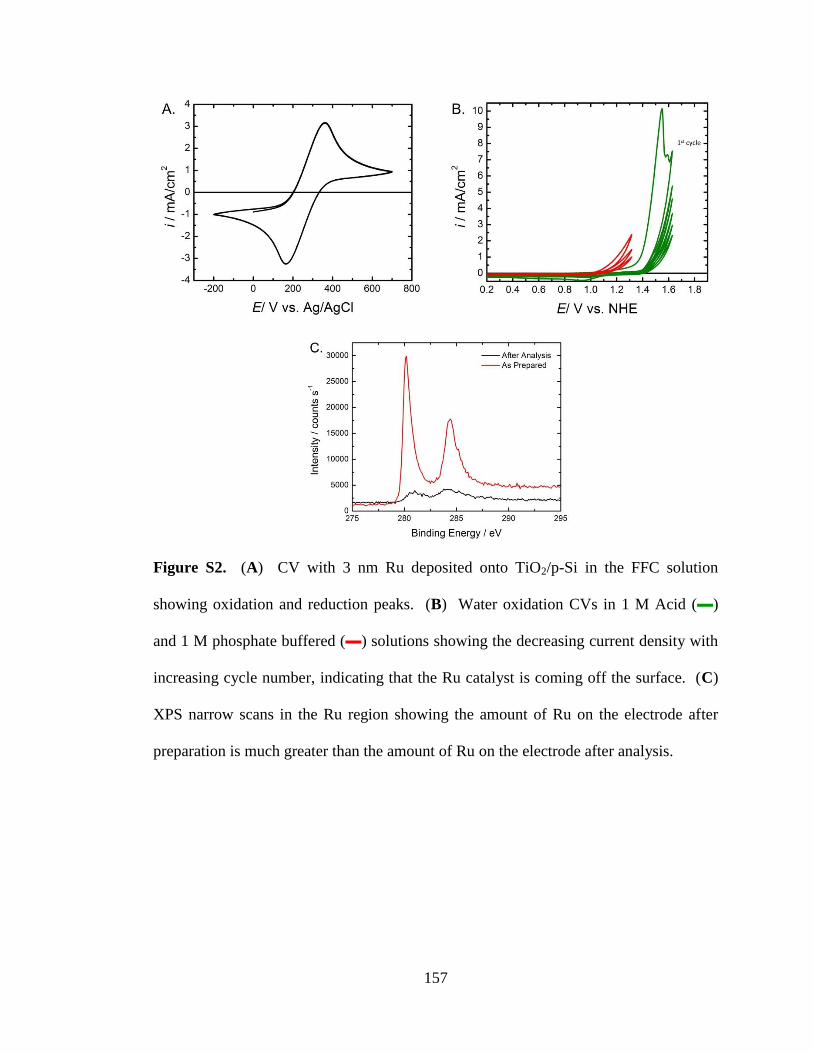
157
Figure S2. (A) CV with 3 nm Ru deposited onto TiO2/p-Si in the FFC solution
showing oxidation and reduction peaks. (B) Water oxidation CVs in 1 M Acid ()
and 1 M phosphate buffered () solutions showing the decreasing current density with
increasing cycle number, indicating that the Ru catalyst is coming off the surface. (C)
XPS narrow scans in the Ru region showing the amount of Ru on the electrode after
preparation is much greater than the amount of Ru on the electrode after analysis.

158
Figure S3. (A) Water oxidation CVs in acidic (), neutral () and basic ()
solutions for a 2 nm Co catalyst layer deposited onto 2 nm TiO2/p-Si. (B) Water
oxidation CVs of the Co layer from (A) with the Co-Pi catalyst deposited in situ.

159
Figure S4. (A) CV of 2 nm of gold deposited onto 2 nm of TiO2/p-Si in FFC solution.
(B) CVs of the gold sample in basic (),neutral () and acidic () solutions for water
oxidation. The results show that the obtained current density is considerably lower than
the values obtained using other water oxidation catalysts.

160
5.10: Supporting Materials References
1. Kanan, M. W.; Nocera, D. G., In situ formation of an oxygen-evolving catalyst
in neutral water containing phosphate and Co2+
. Science 2008, 321, (5892),
1072-1075.