DEVELOPMENT OF MULTISTAGE CUK CONVERTER...
45
DEVELOPMENT OF MULTISTAGE CUK CONVERTER FOR PV VOLTAGE REGULATION WAEL A. Y. SALAH UNIVERSITI SAINS MALAYSIA 2007
Transcript of DEVELOPMENT OF MULTISTAGE CUK CONVERTER...

DEVELOPMENT OF MULTISTAGE CUK CONVERTER FOR PV VOLTAGE REGULATION
WAEL A. Y. SALAH
UNIVERSITI SAINS MALAYSIA
2007
DEVELOPMENT OF MULTISTAGE CUK CONVERTER FOR PV VOLTAGE REGULATION
by
WAEL ABEDL MUHDI YACOUP SALAH
Thesis submitted in fulfillment of the requirements for the degree
of Masters of Science
April, 2007

ii
ACKNOWLEDGEMENTS
This work would never be complete without the mercy of Allah, and Doa’a of
my parents.
I am very grateful to all whom have helped me during this work, and surely
their help and support will always be greatly appreciated.
I would like to thank my advisor Assoc. Prof. Dr. Soib Taib, for his
willingness to work with me and giving me his endless guidance throughout this
project. With his enthusiasm and good humor, Dr. Soib made the study of
power electronics fun and rewarding.
The USM staff also deserve my gratitude, as they work hard to help the
students to reach their goals.
I would like to thank my friends and colleagues in the power lab research
group. It is great to work with a group of people who are so willing to help. I
have enjoyed my time here and wish the good luck to everyone at USM.
I could not have made it without the love and encouragement of my parents,
whom I left in Palestine. It would have been very difficult without their support
and Doa’a to Almighty Allah.
I thank my sisters and brothers; also who were always a source of support
and encouragement. I appreciate all what they have done for me.
Finally, I wish to dedicate this work to my parents, brothers and sisters.

iii
TABLE OF CONTENTS
Page ACKNOWLEDGEMENTS ii
TABLE OF CONTENTS iii
LIST OF TABLES Viii
LIST OF FIGURES ix
LIST OF PLATES xiii
LIST OF SYMBOLS xiv
LIST OF ABBREVIATION xvii
LIST OF PUBLICATIONS & SEMINARS xvii
ABSTRAK xviii
ABSTRACT xx
CHAPTER ONE : INTRODUCTION
1.0 Introduction 1
1.1 Problem Statement 2
1.2 Scope 2
1.3 Objectives 3
1.4 Thesis Layout 3
CHAPTER TWO : LITERATURE REVIEW
2.0 Introduction 5
2.1 Power Supply Rule 5
2.2 DC-DC Converters 6
2.3 Power Supply Types 7

iv
2.3.1 Linear Voltage Regulator 7
2.3.1.1 The Shunt Regulator 8
2.3.1.2 The Series-pass Linear Regulator 8
2.3.2 PWM Switch Mode Power Supply (SMPS) 9
2.3.3 Resonant Converters 13
2.4 Power Supply Basic Topologies 14
2.4.1 Buck Converters 15
2.4.2 Boost Converters 17
2.4.3 Buck Boost Converters 18
2.4.4 Cuk Converter 19
2.5 Transformer Based Topologies 24
2.6 DC Converters and Duty Ratio D 25
2.7 Switching Capacitor Converters 25
2.8 Pulse Width Modulation (PWM) 27
2.9 Losses in PWM Switching 28
2.9.1 Major Losses 28
2.9.2 Losses Associated with the Power Switch 29
2.10 Design Specification 30
2.10.1 Power Switches 30
2.10.2 Diodes 31
2.10.3 MOSFET Gate Driver 33
2.11 Control Principles 34
2.11.1 Voltage-mode Control 35
2.11.2 Current-mode Control 36
2.12 Commercial IC Controller for Switching Converter 37

v
2.12.1 Fixed Frequency Voltage-Mode SG352X PWM Controller
37
2.12.2 Fixed Frequency Current-Mode UC384X PWM Controller
28
2.11.3 Variable Frequency Voltage Mode TL479 Controller 39
2.13 Sensor 40
2.14 Thermoelectric Cooling (TEC) 42
2.14.1 Operation 43
2.14.2 Thermoelectric Cooling Modules 44
2.14.3 TEC Applications 44
2.14.4 TEC Installation 44
2.14.5 TEC Advantages 45
CHAPTER THREE : DESIGN OF THE 3-STAGE NON-INVERTING CUK CONVERTER
3.0 Introduction 47
3.1 Methodology 47
3.2 Switch Capacitor Converters 49
3.3 Design Details 50
3.4 Multistage DC-DC converters 51
3.5 Equivalent Circuits 52
3.5.1 Non-Inverting Cuk Converter 52
3.5.2 Single Stage Non-Inverting Cuk Converter 53
3.5.3 Multistage Non-Inverting Cuk Converter 55
3.6 PWM Switching control and Gate Drive 62
3.7 Voltage Feedback 62

vi
3.8 System Application Load 62
3.9 Determination of Inductors and Capacitors Values 64
3.10 Simulation 65
3.10.1 Simulation Software 66
3.10.2 Circuit Setup 66
3.11 PCB Design 68
CHAPTER FOUR : RESULTS AND DISCUSSION
4.0 Introduction 69
4.1 System Block Diagram 69
4.2 Prototype Assembling 70
4.2.1 Bread boarding Tests 71
4.2.2 System Integration 72
4.3 Switch Selection 75
4.4 Gate Drive Configurations 75
4.5 Data Measurements 76
4.5.1 Measurement Apparatus 76
4.5.2 Temperature Circuit Calibration 77
4.5.3 TEC Tests 78
4.5.4 PV Panel Power Measurement 80
4.5.5 Simulation Results 81
4.5.6 Converter Output Measurement 82
4.5.7 Power and Efficiency 91

vii
CHAPTER FIVE : CONCLUSION
5.0 Multistage Cuk Converter Design 94
5.1 Future Work 95
REFERENCES 97
APPENDICES
Appendix A Simulation Results 102
Appendix B IR2110 MOSFET Driver 113
Appendix C IRFZ44N Data sheet 116
Appendix D LM35 Data sheet 119
Appendix E SG3524 Data sheet 121
Appendix F UC3843 Data sheet 123
Appendix G TL497 Data sheet 125

viii
LIST OF TABLES
Page
Table 2.1 Power supply technologies 14
Table 2.2 Major losses 28
Table 4.1 LM35 test 77
Table 4.2 Maximum Output name plate ratings 80
Table 4.3 Simulation parameters 81

ix
LIST OF FIGURES
Page
Figure 2.1 The basic linear regulator 9
Figure 2.2 Basic forward-mode converter (buck converter) 11
Figure 2.3 Voltage and current waveforms for a forward-mode converter (buck converter)
12
Figure 2.4 Basic flyback-mode converter (boost converter shown) 12
Figure 2.5 Waveforms for a discontinuous-mode boost converter 13
Figure 2.6 B-H plot of symmetrical converters 15
Figure 2.7 Buck converter 16
Figure 2.8 Typical waveforms of buck converter 16
Figure 2.9 Boost (step-up) converter 17
Figure 2.10 Typical waveforms of boost converter 18
Figure 2.11 Buck-boost converter 18
Figure 2.12 Typical waveforms of buck-boost converter 19
Figure 2.13 Cuk converter circuit 20
Figure 2.14 Cuk converter waveforms 20
Figure 2.15 Cuk converter 21
Figure 2.16 Transformerless Cuk PWM converter 21
Figure 2.17 Equivalent circuit of the Cuk converter 22
Figure 2.18 Boost converter followed by a buck converter 22
Figure 2.19 Equivalent circuit with switches 23
Figure 2.20 Single switch equivalent circuit 23
Figure 2.21 Cuk practical realization 23
Figure 2.22 Fixed frequency PWM 27

x
Figure 2.23 Power switch losses 29
Figure 2.24 Switch or diode 31
Figure 2.25 Steady state V-I characteristic of a diode 32
Figure 2.26 Transient V-I characteristic of a diode 33
Figure 2.27 IR2110 DIP14 package 34
Figure 2.28 Functional block diagram 34
Figure 2.29 Voltage-mode control 35
Figure 2.30 Current-mode control 35
Figure 2.31 Temperature Sensor configuration 41
Figure 2.32 Thermal response in still air 42
Figure 2.33 Minimum supply voltage vs. temperature 42
Figure 2.34 Thermoelectric cooling modules 43
Figure 2.35 Typical thermoelectric cooler 44
Figure 2.36 Peltier effect thermoelectric cooler diagram 46
Figure 3.1 Converter design flow chart 48
Figure 3.2 Capacitors charging and discharging 49
Figure 3.3 Charging and discharging state 50
Figure 3.4 Complete system block diagram 51
Figure 3.5 Inverting Cuk converter 52
Figure 3.6 Non-inverting Cuk converter 52
Figure 3.7 Single stage non-inverting Cuk converter 53
Figure 3.8 On-state equivalent circuit 53
Figure 3.9 Off-state equivalent circuit 53
Figure 3.10 Current and voltage waveforms 55
Figure 3.11 Three stage non-inverting Cuk converter 56

xi
Figure 3.12 Off-state power switch losses 56
Figure 3.13 On-state power switch losses 57
Figure 3.14 Conduction modes 60
Figure 3.15 PV connected to converter with the TEC load 63
Figure 3.16 Simulation setup 65
Figure 3.17 Three stage non-inverting cuk converter 67
Figure 3.18 Three Stage non-inverting capacitance voltage divider (S-Off)
67
Figure 3.19 Three Stage non-inverting capacitance voltage divider (S-On)
68
Figure 4.1 System block diagram 69
Figure 4.2 TEC and PV connection 70
Figure 4.3 LM35 temperature versus voltage 78
Figure 4.4 LM35 IC sensor versus thermocouple temperature 78
Figure 4.5 TEC direct measured temperature at cold side 79
Figure 4.6 Load voltage Vo (at 0.5 ohm Load) 81
Figure 4.7 Load current (Io) 82
Figure 4.8 Three stage Cuk converter circuit 83
Figure 4.9 Measured voltage across MOSFET S1 83
Figure 4.10 Simulation waveforms of MOSFET switch S1 84
Figure 4.11 Measured voltage across MOSFET S2 84
Figure 4.12 Simulation waveforms of MOSFET switch S2 85
Figure 4.13 Measured voltage across MOSFET S3 85
Figure 4.14 Simulation waveforms of MOSFET switch S3 86
Figure 4.15 Measured voltage across MOSFET S4 86
Figure 4.16 Simulation waveforms of MOSFET switch S4 87

xii
Figure 4.17 Output diode voltage VDo 87
Figure 4.18 Simulated voltages and current through the output diode Do
88
Figure 4.19 Measured output voltage Vo 88
Figure 4.20 Measured output voltage Vo with Fluke power quality analyzer
89
Figure 4.21 Simulated output voltage and current 89
Figure 4.22 Maximum D 90
Figure 4.23 Minimum D 90
Figure 4.24 Converter efficiency versus load 91
Figure 4.25 Efficiency versus the duty ratio 92
Figure 4.26 Output power versus efficiency 92
xiii
LIST OF PLATES
Page
Plate 3.1 A pre-developed TEC cooling prototype 63
Plate 4.1 MOSFETs driver and PWM circuit bread board 71
Plate 4.2 Power circuits board connected to control circuit 71
Plate 4.3 Power circuit PCB 72
Plate 4.4 Power circuit PCB with MOSFET driver circuit 72
Plate 4.5 DC-DC converter 18V supply with R-load 73
Plate 4.6 Temperature monitor circuit 73
Plate 4.7 TEC modules attached to heat sink 74
Plate 4.8 TEC modules attached to heat sink and AL sheet 74
Plate 4.9 Gating driver and isolation circuit 75
Plate 4.10 FLUKE 43B power quality analyzer 76
Plate 4.11 Traditional oscilloscope 76
Plate 4.12 TEC module with the heat sink 79
Plate 4.13 BP solar module 80

xiv
LIST OF SYMBOLS
Page
1CV Capacitor number 1 voltage (refer Figure 3.14) 54
CI Collector current of BJT. 29
CEV Collector to emitter voltage of BJT. 29
Li Converter input inductor 54
oL Converter output inductor 55
Li Current through inductor 61
lR DC resistance of the inductor. 61
FV Diode voltage drop at ( )maxLI 61
DI Drain current of MOSFET switch 29
)(onDSR Drain to source On-resistance 54
D Duty ratio percentage (%) 17
ft Fall time of MOSFET switch 61
f Frequency 61
L Inductor general symbol 61
.initi Initial transient time 28
inV Input voltage of DC-DC converter in Volts (V) 18
maxD Maximum duty cycle 61
( )maxiV Maximum input voltage 61
minD Minimum duty ratio 61
( )miniV Minimum input voltage 61

xv
oV Output v voltage 20
oV Output voltage by neglecting losses 61
*oV Output voltage under losses consideration 61
outV Output voltage of DC-DC converter in Volts (V) 18
)(conductDP Power loss during conduction time 29
rt Rise time of MOSFET switch 61
Vs Supply voltage 20
offt Switching Off-time 27
ont Switching ON-time 28
( )totoalont Total On-time of MOSFET switch 61
T Total switching time 18
( )OffDt Turn Off delay time 59
( )offLiv Voltage across input inductor during switching Off - state 58
( )onLiv Voltage across input inductor during switching On - state 58
1SV Voltage across MOSFET switch S1. 57
2SV Voltage across MOSFET switch S2. 57
( )onLov Voltage across output inductor during switching ON -state 58
( )offLov Voltage across output inductor during switching ON -state 58
RDV Voltage across the diode resistance 58
RsV Voltage across the ON-resistance of MOSFET switch 58
swV Voltage drop across the switch 61
LV Voltage drop in resistance of inductor 61
xvi
LIST OF ABBREVIATION
Page
AC Alternating Current 5
CAD Computer Aided Design 65
DC Direct Current 5
IC Integrated Circuit 37
IEEE Institute of Electrical and Electronic Engineering 107
IR International Rectifier 34
MOSFET Metal Oxide Field Effect Transistor 33
MTBF Mean Time Between Frailer 43
PCB Printed Circuit Board 68
PV Photovoltaic 3
PWM Pulse Width Modulation 10
RTD Resistance Temperature Detector 40
SC Switching Converters 47
SCC Switch Capacitor Converter 26
SIMCAD Simulation of Computer Aided Design 65
SMPC Switch Mode Power Converter 9
SMPS Switch Mode Power Supply 1
SPS Switching Power Supply 7
TEC Thermo Electric Cooler 42
xvii
LIST OF PUBLICATIONS & SEMINARS
Page
1 Salah, W., Taib, S. (2006). Improvement of Transformerless 200W SMPS Using CUK DC-DC Converter. First IEEE International Power and Energy Conference, PECon 2006. Putrajaya, Malaysia. 28-29 November, 2006.
127
2 Taib, S., Anwar, A., Salah, W. (2006). Energy Efficiency Practice: Concept, Indicator and Benefit. JSPS-VCC Group Seminar 2006, National Resources and Energy Environment. Johor Bahru, Malaysia. 11-12 December, 2006.
128
3 Al-Mofleh A., S Taib, and Salah, W. (2007). Energy Policy and Energy demand for Malaysian Development Energy Efficiency. First Power Engineering and Optimization Conference 2007, PEOCO2007. Shah Alam, Malaysia. 6th June 2007.
129

xviii
PEMBANGUNAN PENUKAR CUK PELBAGAI ARAS UNTUK PENGAWALAN VOLTAN PV
ABSTRAK
Tesis ini mengemukakan reka bentuk pengubah SPMS untuk aplikasi berkuasa
rendah.Litar penukar adalah berdasarkan topologi CUK yang secara asasnya
ialah kombinasi topologi penukar “buck” dan “boost”. Topologi penukar yang
dicadangkan adalah berdasarkan junaman masukan voltan ke dalam peranti
penyimpanan dalam keadaan pengecasan dan menghantar tenaga yang
disimpan dalam keadaan penyahcasan. Proses ini akan beroperasi pada
kelajuan tinggi untuk memastikan pengaliran arus beban yang berterusan.
Penukar yang rekabentuk mampu menukar masukan voltan arus terus melalui
pemengal voltan pelbagai peringkat. Penghantaran tenaga dilakukan melalui
elemen kapasitif untuk memastikan riak arus beban yang minimum. Pensuisan
pantas dan rintangan yang rendah dari MOSFET berkuasa tinggi digunakan
untuk menurunkan voltan. Suis berkuasa tinggi beroperasi pada frekuensi yang
tinggi dan kawalan IC SG3524 PWM digunakan untuk memberikan denyut
isyarat pengoperasian untuk pensuisan. Hasil simulasi menunjukkan penukar
boleh membekalkan kuasa ke beban sehingga 100 Watt dengan 90%
kecekapan parameter berdasarkan nilai unggul dan beban terkadar daripada
sel PV. Keputusan simulasi, menujukkan penukar boleh beroperasi dengan baik
pada frekuensi pensuisan yang tinggi sehingge 500KHz. Bagi meminimumkan
tekanan terhadap suis MOSFET, frekuensi yang digunakan oleh penukar ialah
200kHz.
Komponen litar yang dipilih memberikan kadar pensuisan dan kehilangan
kealiran yang minimum.

xix
Secara praktikalnya, penukar berfungsi pada kecekapan kuasa sebanyak 80%
untuk beban 70Watt dan sesuai untuk applikasi TEC.

xx
DEVELOPMENT OF MULTISTAGE CUK CONVERTER FOR PV VOLTAGE REGULATION
ABSTRACT
This thesis presents the design of a transformerless SMPS for low power
applications. The converter circuit is based on CUK topology which is basically
a combination of buck and boost converter topologies. The proposed converter
topology is based on dividing the input voltage into storage devices as charging
state and delivering the stored energy to the load in the discharging state. This
process is operates at high speed to ensure continuous conduction of load
current. The developed converter converts input DC voltage throughout
multistage voltage chopping. The transfer of energy through the capacitive
elements ensures that the load current is almost ripple free. Fast switching and
low On-resistance power MOSFETs were used to step down the input voltage.
The power switches operated at high frequency, and the PWM control IC was
used to provide the operating signal for the switch.
The simulation results show, that the converter had the capability to supply
the load of power up to 100W with an efficiency of 90% under ideal parameters
using rated load supplied from PV cell. The results show that the converter
could operate properly at high switching frequency up to 500KHz. For the
purpose of minimization of the stress on MOSFET switches, the frequency used
for implementation of the converter was 200KHz. The circuit components were
selected to reduce the switching and conduction losses. Practical
implementation of the converter shows that the converter operated at an
efficiency of 80% at 70W load, and suitable for TEC application.

1
CHAPTER 1 INTRODUCTION
1.0 Introduction
Power supply is a buffer circuit that provides power, required by the load
from a primary power source with characteristics incompatible with the load. It
makes the load compatible with its power source. A Power supply is also known
as a power converter and the process is called power conversion. It is also
called a power conditioner and the process is called power conditioning.
Power supply can be defined as a device that converts the available power
of one set of characteristics to another set of characteristics to meet the
specified requirements. Typical application of power supplies includes the
conversion of a raw input voltage to a controlled or stabilized voltage for the
operation of electronic equipment.
Switch mode power supplies (SMPS) can be used in applications of high
current drain which require a low stable supply voltage. Switching power
supplies are of highly efficient devices.
The essential feature of a switch mode regulation of DC voltages is that the
load is connected to the power source at regular intervals by a semiconductor
switch, and then disconnected. The mean value of the voltage applied to the
load is maintained at a nearly constant level by an automatic regulation circuit
that vary the duration of On and Off periods of the power switch.

2
1.1 Problem Statement
SMPS occupies between the two type of converters namely, the line
regulated and resonant converters. The main problem of the line regulator is
high power losses which is being dissipated mainly as heat, and the efficiency
level is very low, at around only 40%. On the other hand this type of regulators
are cheap and simple, relative to resonant converters which are complex and
expensive but are highly efficient.
The switching converter is a good choice for many applications, and so the
development of this converter was the object under interest. The existence of a
transformer in DC-DC conversion process of switching converter, would limit the
control range of duty ratio to a small value (Middlebrook, 1988).
The primary design problem of the system was to interconnect the converter
components and to control the switches, so that desired results can be
obtained. The secondary design problem was to avoid using loose components
that will affect the converter performance and characteristics.
1.2 Scope
Nowadays all applications emphasize on efficiency. Switch mode power
supply (SMPS) design minimizes the use of loose components such as
resistors and use components that are ideally lossless, such as switches,
capacitors, inductors, and transformers. This project concentrates on usage of
power storage elements in the implementation of a power conversion process,
and then transferring the stored energy to the load.
The design of the switching converter and the selection of switching
elements and their configuration was the highest challenge. The simulation test

3
has to be done under ideal considerations, so that the implementation and
fabrication of hardware will be the real challenge. A proper topology and control
was chosen that would exceed the performance requirements.
1.3 Objectives
The design process was considered successful when a proper topology and
control had been chosen to exceed the performance requirements and when
protection techniques and parts were selected to exceed the required reliability.
So the main objective will be:
• To select a proper topology for DC-DC converter.
• To select suitable components for converter that ensures the best
performance.
• To develop a DC converter that is compatible with photovoltaic (PV) as a
source for input power.
• To develop a power supply that is capable to supply TEC load.
• To avoid the use of transformers in DC-DC conversion process.
• To have a power supply with relatively good efficiency.
• To develop a cooling system for the telecommunication cabinets cooling
applications.
1.4 Thesis Layout
The thesis chapters are arranged in such away that the project work details
have been clearly presented. The thesis was arranged in five chapters namely:
Introduction, Literature Review, Design of the 3-Stage Non-inverting Cuk
Converter, Results and Discussion and ended with the Conclusion.
4
An introduction to power supply, the objectives of the project and proposed
solutions were illustrated with a scope of the basic topology of Cuk converter
and multistage converters in the fist chapter.
Although many topologies are introduced in the implementation of DC-DC
converters, basically they categorized into three main topologies, which are
Buck (step-down), Boost (step-up) and buck-boost (step up/down) converters.
Chapter 2 presents an introduction and a review of power supply main
topologies, a general scope on DC-DC converters, and thorough details on the
topology circuits and waveforms, and theories of such converters. The position
of the switching capacitor converter among other topologies is illustrated with
comparison of advantages and disadvantages of each topology.
The approaches and methods of this project has been explained thoroughly
in Chapter 3. The chapter starts with an introduction to the basic switch
capacitor converter topology and then goes to the basic Cuk converter topology
configuration. The details of the DC-DC conversion process are illustrated
clearly.
The results and discussion are presented in Chapter 4where all the details of
project simulation and experimental results are illustrated with figures,
waveforms and plates. The discussion and summary of this chapter would be
presented at the end of the chapter.
Finally, Chapter 5, the conclusion chapter provides the overview of the
objectives achieved by this project, and it also provides suggestions and
recommendations for future work.

5
CHAPTER 2 LITERATURE REVIEW
2.0 Introduction
A power supply assumes a very unique role within a typical system. It can be
considered as the mother of the system. It gives the system life by providing
consistent and repeatable power to its circuits. It defends the system against
the harsh world outside the confines of the enclosure and protects its wards by
not letting them to do harm to themselves. If the supply has a failure within
itself, it must fail gracefully and not allow the failure to reach the system
(Ferenczi, 1987).
Power processing is an essential stage of most electrical equipments. The
differences in voltages and currents requiremed for different applications led to
the design of special power converters (Tse, et al., 1994).
Generally power conversion process involves either converting alternating
(AC) to direct current (DC) or converting DC of one voltage level to other
voltage level depending on the application requirements (Ferenczi, 1987).
2.1 Power Supply Rule
The primary function of a power supply is to hold the voltage in its output
circuit at predetermined value over the expected range of load currents. The
degree of which the power supply is able to maintain constant voltage against
variation in load current, input voltage and temperature will determine the
quality of the designed power supply.

6
The power supply has been considered as the heart of any electrical system,
and so it plays an important role. The quality of power conversion highly affects
the overall performance of the system (www.psma.com).
2.2 DC-DC Converters
DC conversion is of great importance in many applications, starting from low
power applications to high power applications. The goal of any system is to
emphasize and achieve the efficiency to meet the system needs and
requirements. Several topologies have been developed in this area, but all
these topologies can be considered as apart or a combination of the basic
topologies which are buck, boost and flyback (Rashid, 2001).
For low power levels, linear regulators can provide a very high-quality output
voltage. For higher power levels, switching regulators are used. Switching
regulators use power electronic semiconductor switches in On and Off states.
Because there is a small power loss in those states (low voltage across a switch
in the On state, zero current through a switch in the Off state), switching
regulators can achieve high efficiency energy conversion (Rashid, 2001).
The functions of dc-dc converters are:
1- Convert a DC input voltage Vs into a DC output voltage Vo.
2- Regulate the DC output voltage against load and line variations.
3- Reduce the AC voltage ripple on the DC output voltage below the required
level.
4- Provide isolation between the input source and the load (if required).

7
5- Protect the supplied system and the input source from electromagnetic
interference (EMI) (Krein, 1998).
The DC-DC converter is considered as the heart of the power supply (Perez,
2000), thus it will affect the overall performance of the power supply system.
The converter accepts DC and produces a controlled DC output.
2.3 Power Supply Types
The three major power supply technologies that can be considered within a
power supply system are:
1. Linear voltage regulators.
2. Pulse-width modulated (PWM) switching power supplies.
3. High efficiency resonant technology switching power supplies.
2.3.1 Linear Voltage Regulator
The linear regulator is the original form of the regulating power supply. It
relies upon the variable conductivity of an active electronic device to drop
voltage from an input voltage to a regulated output voltage (Brown, 1994).
The linear regulator wastes a lot of power in the form of heat, and therefore
gets hot. The linear power supply finds a very strong niche within applications
where its inefficiency is not important and also where low cost and a short
design period are desired. The linear regulator is sometimes referred as
dissipative regulator (Sum, 1984). These include wall-powered, ground-base
equipment where forced air cooling is not a problem, and also those
applications in which the instrument is so sensitive to electrical noise that it
requires an electrical “quiet” power supply. These products might include audio
8
and video amplifiers, RF receivers, and so forth. Linear regulators are also
popular as local, board-level regulators. Here only a few watts are needed by
the board, so the few watts of loss can be accommodated by a simple heat-sink
(Brown, 1990).
Linear regulators can only produce output voltages lower than their input
voltages and each linear regulator can produce only one output voltage. Each
linear regulator has an average efficiency of between 35 and 50 percent; the
losses are dissipated as heat.
Linear regulators are step-down regulators only; that is, the input voltage
source must be higher than the desired output voltage. There are two types of
linear regulators: the shunt regulator and the series-pass regulator (Rashid,
2004).
2.3.1.1 The shunt regulator
It is a voltage regulator that is placed in parallel with the load. An
unregulated current source is connected to a higher voltage source, the shunt
regulator draws output current to maintain a constant voltage across the load
and gives a variable input voltage and load current. A common example of this
is a zener diode regulator (Ang and Oliva, 2005).
2.3.1.2 The series-pass linear regulator
Comparatively this is more efficient than the shunt regulator and uses an
active semiconductor as the series-pass unit between the input source and the
load. In general, the linear regulator is quite useful for those power supply
applications requiring less than 10W of output power. Above 10W the heat-sink
9
required becomes so large and expensive that a switching power supply
becomes more attractive (Ang and Oliva, 2005).
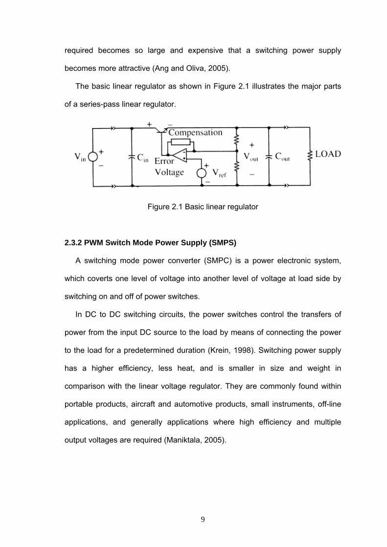
The basic linear regulator as shown in Figure 2.1 illustrates the major parts
of a series-pass linear regulator.
Figure 2.1 Basic linear regulator
2.3.2 PWM Switch Mode Power Supply (SMPS)
A switching mode power converter (SMPC) is a power electronic system,
which coverts one level of voltage into another level of voltage at load side by
switching on and off of power switches.
In DC to DC switching circuits, the power switches control the transfers of
power from the input DC source to the load by means of connecting the power
to the load for a predetermined duration (Krein, 1998). Switching power supply
has a higher efficiency, less heat, and is smaller in size and weight in
comparison with the linear voltage regulator. They are commonly found within
portable products, aircraft and automotive products, small instruments, off-line
applications, and generally applications where high efficiency and multiple
output voltages are required (Maniktala, 2005).

10
a) Principle of Operation
The operation of switching power supplies can be relatively easy to
understand. Unlike linear regulators which operate the power transistor in the
linear mode, the PWM switching power supply operates the power transistors in
both the saturated and cutoff states. In these states, the volt-ampere product
across the power transistor is always kept low (saturated, low-voltage / high-
current; and cutoff, high-voltage / No-current). This product within the power
device is the loss within all the power semiconductors (Hnatek, 1989).
This more efficient operation of the PWM switching power supply is done by
“chopping” the direct current (DC) input voltage into pulses whose amplitude is
the magnitude of the input voltage and whose duty cycle is controlled by a
switching regulator controller. These AC waveforms are then filtered to provide
the DC output voltages (Pressman, 1998). The controller; main purpose is to
maintain a regulated output voltage and operates like a linear style controller.
That is, the functional blocks, voltage reference, and error amplifier are
arranged identical to the linear regulators. The difference in the output of the
error amplifier (the error voltage) is then placed into a voltage-to-pulse-width
converter stage prior to driving the power switches (Brown, 1994).
b) Operational Types
There are two major operational types of switching power supplies: the
forward-mode converter and the Fly back Mode Converter. Although the
arrangements of their parts are subtly different, their operation is very different
and each has advantages in certain areas of application (Brown, 1990).

11
i) The Forward Mode Converter
Forward-mode regulators form a large family of switching power supply
topologies. They can be recognized by an L-C filter just after the power switch
or after the output rectifier on the secondary of a transformer. A simple form of
the forward-mode regulator can be seen in Figure 2.2. This is called the buck
regulator (Mohan et al., 2003).
Figure 2.2 Basic forward-mode converter (buck converter).
Its operation can be seen as analogous to a mechanical flywheel and a one
piston engine. The L-C filter, like the flywheel, stores energy between the power
pulses of the driver. The input to the L-C filter (choke input filter) is the chopped
input voltage. The L-C filter volt-time averages this duty-cycle modulated input
voltage waveform.
The output voltage is maintained by the controller by varying the duty cycle.
The buck converter is also known as a step-down converter, since its output
must be less than the input voltage. The operation of the buck regulator can be
seen by breaking its operation into two periods as shown in Figure 2.3. When
the switch is turned on, the input voltage is presented to the input of the L-C
filter.

12
Figure 2.3 Voltage and current waveforms for a forward-mode converter (buck
converter).
ii) The Flyback Mode Converter
The second family of converters is the flyback (boost) mode converters. The
most elementary flyback-mode (or boost-derived) converter can be seen in
Figure 2.4. It is called a boost converter (Ang and Oliva, 2005).
Figure 2.4 Basic flyback-mode converter (boost converter shown).
The boost-mode converter has the same parts as the forward-mode
converter, but they have been rearranged. This new arrangement causes the
converter to operate in a completely different fashion than the forward-mode
converter. This time, when the power switch is turned on, a current loop is
13
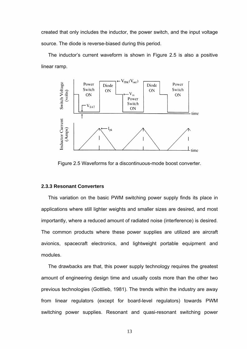
created that only includes the inductor, the power switch, and the input voltage
source. The diode is reverse-biased during this period.
The inductor’s current waveform is shown in Figure 2.5 is also a positive
linear ramp.
Figure 2.5 Waveforms for a discontinuous-mode boost converter.
2.3.3 Resonant Converters
This variation on the basic PWM switching power supply finds its place in
applications where still lighter weights and smaller sizes are desired, and most
importantly, where a reduced amount of radiated noise (interference) is desired.
The common products where these power supplies are utilized are aircraft
avionics, spacecraft electronics, and lightweight portable equipment and
modules.
The drawbacks are that, this power supply technology requires the greatest
amount of engineering design time and usually costs more than the other two
previous technologies (Gottlieb, 1981). The trends within the industry are away
from linear regulators (except for board-level regulators) towards PWM
switching power supplies. Resonant and quasi-resonant switching power
14
supplies are emerging slowly as the technology matures and their designs are
made easier (Luecke, 2005).
Table 2.1 shows a comparison between the last three technologies, referring
to their cost, weight, efficiency, and development difficulties.
Table 2.1 Power supply technologies
Cost Weight Efficiency Development
Difficulties
Linear Regulator Low High 34-50% Simple
PWM Switch Mode
converter High Low-Medium 70-85% Medium
Resonant Switch
mode converter Highest Low-Medium 78-92% Hard
Resources: Marty Brown, Power Supply Cookbook, 1994.
2.4 Power supply Basic Topologies
Whittington, (1992) presents an overview of the most important DC-DC
converter topologies. The main objective is to guide the designer in selecting
the topology with its associated power semiconductor devices. The DC-DC
converter topologies can be divided into two major parts, depending on whether
or not they have isolated between the input supply and the output circuitry.
Non - Isolated Switching Regulators:
According to the position of the switch and the rectifier, different types of
voltage converters can be made:
- Step down “Buck” regulator
- Step up “Boost” regulator
15
- Step up / Step down “Buck - Boost” regulator
- Transfromerless CUK Converter
Isolated Converters
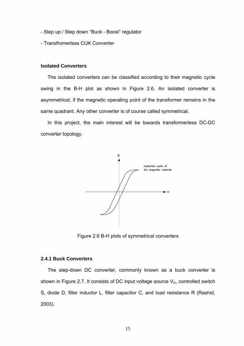
The isolated converters can be classified according to their magnetic cycle
swing in the B-H plot as shown in Figure 2.6. An isolated converter is
asymmetrical, if the magnetic operating point of the transformer remains in the
same quadrant. Any other converter is of course called symmetrical.
In this project, the main interest will be towards transformerless DC-DC
converter topology.
Figure 2.6 B-H plots of symmetrical converters
2.4.1 Buck Converters
The step-down DC converter, commonly known as a buck converter is
shown in Figure 2.7. It consists of DC input voltage source Vin, controlled switch
S, diode D, filter inductor L, filter capacitor C, and load resistance R (Rashid,
2003).

16
Figure 2.7 Buck converter
Typical waveforms in the converter are shown in Figure 2.8 under the
assumption that the inductor current is always positive (Trzynadlowski, 1998).
The state of the converter in which the inductor current is never zero for any
period of time is called the continuous conduction mode (CCM). It can be seen
from the circuit that when the switch S is commanded to the On state, the diode
D is reverse-biased. When the switch S is Off, the diode conducts to support an
uninterrupted current in the inductor.
Figure 2.8 Typical waveforms of buck converter

17
The relationship among the input voltage, output voltage, and the switch duty
ratio D can be derived, based on the Faraday’s law i.e., the inductor volt-second
product over a period of steady-state operation is zero.
2.4.2 Boost Converters
A step-up or a PWM boost converter as shown in Figure 2.9 consists of DC
input voltage source Vin, boost inductor L, controlled switch S, diode D, filter
capacitor C, and load resistance R (Rashid, 2003). The converter waveforms in
the continuous conduction mode are presented in Figure 2.10.
Figure 2.9 Boost (step-up) converter
When the switch S is in the on state, the current in the boost inductor
increases linearly and the diode D is off at that time. When the switch S is
turned off, the energy stored in the inductor is released through the diode to the
output RC circuit.

18
Figure 2.10 Typical waveforms of boost converter
2.4.3 Buck Boost Converters
A non-isolated (transformerless) topology of the buck-boost converter is
shown in Figure. 2.11. The converter consists of DC input voltage source Vin,
controlled switch S, inductor L, diode D, filter capacitor C, and load resistance
R. With the switch on, the inductor current increases while the diode is
maintained off. When the switch is turned off, the diode provides a path for the
inductor current (Schuler, 2003; Brown, 1994).
Figure 2.11 Buck-boost converter

19
The polarity of the diode that results in its current is being drawn from the
output. The buck-boost converter waveforms are depicted in Figure 2.12. The
output voltage Vo is negative with respect to the ground. Its magnitude can be
either greater or smaller (equal at D = 0.5) than the input voltage as the name of
the converter implies.
Figure 2.12 Typical waveforms of buck-boost converter
2.4.4 Cuk Converters
The buck, boost and buck-boost converters all transfers energy between
input and output using the inductor, analysis being based on the voltage
balance across the inductor. The Cuk converter uses the capacitor for energy
transfer and the analysis is based on the current balance of the capacitor
(Chryssis, 1984; Middlebrook, 1998).
a) CUK circuit and waveforms
The circuit of the Cuk converter is shown in Figure 2.13 consists of DC input
voltage source Vs, input inductor L1, controllable switch S, energy transfer

20
capacitor C1, diode D, filter inductor L2, filter capacitor C, and load resistance
R. An important advantage of this topology is a continuous current at both the
input and the output of the converter. Disadvantages of the Cuk converter are a
high number of reactive components and high current stresses on the switch,
the diode, and the capacitor C1.
Figure 2.13 Cuk converter circuit
The main waveforms of the converter are presented in Fig. 2.14. When the
switch is on, the diode is off and the capacitor C1 is discharged by the inductor
L2 current. With the switch in the off state, the diode conducts currents of the
inductors L1 and L2, whereas capacitor C1 is charged by the inductor L1
current (Rashid, 2004; Ang, 1995).
Figure 2.14 Cuk converter waveforms
21
b) CUK converter operation
The DC transfer function for the buck, boost, and Cuk PWM DC-DC
converters in continuous conduction mode are, D , l / ( l - D ) , and –D /( l - D)
respectively, where D is the duty cycle. Therefore the Cuk PWM DC-DC
converter circuit can be synthesized by cascading boost and buck converter
circuits (Bryant and Kazimierczuk, 2003; Beil et al., 1999).
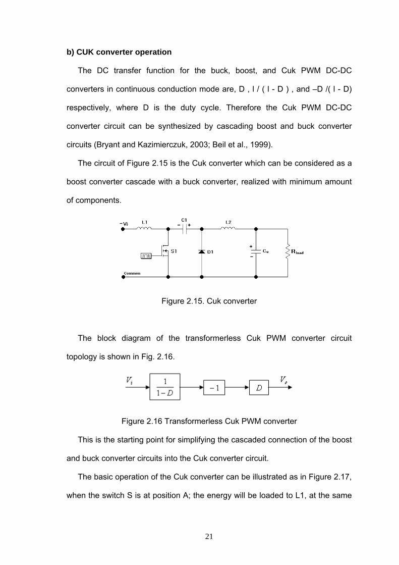
The circuit of Figure 2.15 is the Cuk converter which can be considered as a
boost converter cascade with a buck converter, realized with minimum amount
of components.
Figure 2.15. Cuk converter
The block diagram of the transformerless Cuk PWM converter circuit
topology is shown in Fig. 2.16.
Figure 2.16 Transformerless Cuk PWM converter
This is the starting point for simplifying the cascaded connection of the boost
and buck converter circuits into the Cuk converter circuit.
The basic operation of the Cuk converter can be illustrated as in Figure 2.17,
when the switch S is at position A; the energy will be loaded to L1, at the same

22
time the energy stored in C1 will be discharged to the load Ro, through the low-
pass filter Lo-Co.
Figure 2.17 Equivalent circuit of the Cuk converter
c) Cuk converter derivation
In 1978, the US Patent Office granted Dr Slobodan Cúuk of CalTech
(pronounced Chook) a patent for the design of a new SMPS topology. The
benefits of his new topology includes increased efficiency, low input and output
current ripple, minimal RFI and small size and weight (www.psma.com).
The figures below, show how the Cuk circuit is derived. Firstly, consider a
boost converter followed by a buck converter as shown in Figure 2.18.
Figure 2.18 Boost converter followed by a buck converter
If the diodes are considered as switches, then the two switch-and diode sets
could be replaced with a Double Pole, Double Throw ( DPDT) switch as shown
in Figure 2.19.

23
Figure 2.19 Equivalent circuit with switches
The DPDT switch and shunt capacitor can be replaced with a Single Pole,
Single Throw (SPST) switch and series capacitor, provided a reverse of output
polarity is accepted, as shown in Figure 2.20.
Figure 2.20 Single switch equivalent circuit
The circuit shown in Figure 2.20 is an example of a Cuk converter. A
practical realization could be as shown in Figure 2.21.
Figure 2.21 Cuk practical realization
24
The DC voltage transformation ratio M is M=D/D', where D is the duty ratio
(fractional on-time) of the transistor switch operated at a switching frequency
1/Ts, and D'=1-D is the complementary duty ratio (fractional off-time).
For a DC input voltage Vi, the output voltage is Vo=MVi. The converter thus
has a step down ratio for D<0.5 and a step-up ratio for D>0.5. The other
principal feature is that both the input and output currents are non-pulsating,
both being smoothed by the input and output inductors. These inductors also
eliminate current surges in the transistor switch at power-on and power-off,
which is often a difficult problem to solve.
The output capacitance C2 is usually included to absorb the load current
fluctuations. The Cuk converter is unique because of the capacitive energy
transfer from the input to the output instead of inductive energy transfer
converters. Therefore capacitive energy transfer is more effective in comparison
with the unit size or weight basis than the inductive energy transfer (Yaskiv,
2001).
Because the input and output inductor currents are essentially constant, the
switching current is confined entirely within the converter in the transistor
coupling capacitor-diode loop. With careful layout this loop can be made
physically small, in order to reduce the radiated RFI from the magnetic field
(Wanior, 2003).
2.5 Transformer Based Topologies
Other topologies for DC-DC converters also exist. These are transformer
based topologies. The following are a list of these topologies (Whittington et al.,
1992; Krein, 1998).