
DEVELOPMENT OF A 180° HYBRID BALUN TO FEED A …
52
DEVELOPMENT OF A 180° HYBRID BALUN TO FEED A TIGHTLY COUPLED DIPOLE X-BAND ARRAY Senior Honors Thesis Presented in Partial Fulfillment of the Requirements for Graduation with Distinction in the College of Engineering of The Ohio State University By Nathanael J. Smith The Ohio State University 2010 Honors Thesis Committee: Dr. John Volakis, Adviser Dr. Chi-Chih Chen, Co-Adviser
Transcript of DEVELOPMENT OF A 180° HYBRID BALUN TO FEED A …
DEVELOPMENT OF A 180° HYBRID BALUN TO FEED A TIGHTLY
COUPLED DIPOLE X-BAND ARRAY
Senior Honors Thesis
Presented in Partial Fulfillment of the Requirements for Graduation with Distinction in
the College of Engineering of The Ohio State University
By
Nathanael J. Smith
The Ohio State University
2010
Honors Thesis Committee:
Dr. John Volakis, Adviser
Dr. Chi-Chih Chen, Co-Adviser

Copyright by
Nathanael J. Smith
2010

ii
Abstract
In contrast to conventional arrays, tightly coupled dipole arrays have been shown
to provide enhanced broadband (4:1 performance) when placed near a conductive ground
plane. However, such arrays cannot practically realize their full bandwidth with
integrated feeding elements due to current design limitations. Such feeds also do not
fully address the common mode problem which occurs at certain frequencies in the active
array. In this effort, we propose and study several feed designs aimed at creating a wide
band 180° hybrid balun. It is demonstrated that shielded structures that are not
wavelength restrictive can be realized without exciting the troublesome common mode.
The presented balun design provides a transition from 100Ω fed twin wire to 50Ω dual
enclosed printed stripline that feeds the densely populated dipole array.

iii
Acknowledgments
The author would like to thank Doctorial Candidate Mr. Justin Kasemodel for his
time in training the author, and helpful discussions which were instrumental in my pursuit
of this undergraduate research and the compilation of this thesis. Thanks also goes to Dr.
John Volakis and Dr. Chi-Chih Chen for their mentoring through this research. Thanks
to The Ohio State University for a scholarship grant to pursue this research as well as my
friends and family that were supportive and helped with the proofreading of this thesis.

iv
Vita
1986 ............................................................ Born
2010 ............................................................ B.S. Electrical & Computer Engineering
The Ohio State University
Columbus, OH
Fields of Study
Major Field: Electrical and Computer Engineering
Studies in:
Computers
Analog Circuits
Electromagnetism

v
Table of Contents
DEVELOPMENT OF A 180° HYBRID BALUN TO FEED A TIGHTLY COUPLED
DIPOLE X-BAND ARRAY ............................................................................................1
Senior Honors Thesis .......................................................................................................1
Abstract .......................................................................................................................... ii
Acknowledgments ......................................................................................................... iii
Vita ............................................................................................................................... iv
Fields of Study .............................................................................................................. iv
Table of Contents ............................................................................................................v
List of Figures .............................................................................................................. vii
CHAPTER 1: INTRODUCTION .................................................................................. 10
1.1. Motivation ....................................................................................................... 10
1.3. Organization of Thesis ..................................................................................... 13
CHAPTER 2: TCDA COMMON MODE PROBLEM ................................................... 13
2.1. Tightly Coupled Dipole Array ............................................................................. 13
2.2. Twin Wire Feed and Common Mode Problem ..................................................... 16
2.3. Dual Coaxial Balanced Feed................................................................................ 20
CHAPTER 3: WAVELENGTH BASED HYBRID AND GAP HYBRID ...................... 23
3.1. Raytheon Tapered Hybrid.................................................................................... 23

vi
3.2. Microstrip Delay Line Hybrid ............................................................................. 25
3.3. Gap Phase Reversal Hybrid ................................................................................. 26
CHAPTER 4: ENCLOSED STRIPLINE TO DUAL ENCLOSED STRIPLINE 180°
HYBRID ....................................................................................................................... 32
4.1. Enclosed Stripline to Twin Wire Analysis ........................................................... 32
4.2. Quantifying Phase and Amplitude Unbalance of a Twin Wire Transmission Line.
.................................................................................................................................. 36
4.3. Twin Wire to Dual Enclosed Stripline Analysis ................................................... 41
4.4. Enclosed Stripline to Dual Enclosed Stripline Mated ........................................... 47
CHAPTER 5: CONCLUSION AND FUTURE WORK ................................................. 49
REFERENCES .............................................................................................................. 51

vii
List of Figures
Figure 1: Unbalanced coaxial line with equivalent circuit (edited figure from [2]) ......... 12
Figure 2: Tapered coaxial balun transformer [3]
.............................................................. 12
Figure 3: Unit cell model and 4x4 array of TCDA ......................................................... 14
Figure 4: (a) Active |Γ| for TCDA (b) Smith Chart for TCDA normalized to 200Ω ........ 15
Figure 5: Magnitude of E at 2.5 GHz in the x-z plane .................................................... 16
Figure 6: (a) Unit cell of twin wire fed dipole (b) Twin wire top view diameter and
spacing .......................................................................................................................... 17
Figure 7: Dipole surface vector current (a) Common mode at 1.906GHz (b) Differential
mode at 1.85GHz ........................................................................................................... 19
Figure 8: (a) Active |Γ| (b) Realized gain co-polarization and cross-polarization ............ 19
Figure 9: Dual coaxial balanced feed ............................................................................. 21
Figure 10: Coaxial feed (a) Active |Γ| (b) Realized gain co-polarization and cross-
polarization.................................................................................................................... 21
Figure 11: 4 port enclosed unit cell ideal feeding system................................................ 22
Figure 12: (a) Front view of coax feed from Figure 11 (b) Top view of dipole antenna
feed ............................................................................................................................... 23
Figure 13: Raytheon based 180° hybrid ......................................................................... 23
Figure 14: Raytheon Tapered Hybrid S-Parameters (a) Magnitude (b) Phase ................. 24
Figure 15: Microstrip Delay Line Hybrid ....................................................................... 25
Figure 16: (a) Amplitude unbalance for delay line hybrid |S21|-|S31| (b) Phase difference
for delay line hybrid phase(S12)-phase(S31).................................................................. 26
viii
Figure 17: Gap phase reversal concept with E-field vectors ........................................... 27
Figure 18: Gap phase reversal hybrid ............................................................................. 28
Figure 19: Gap phase reversal hybrid (a) Surface current plot (b) S-Parameter magnitude
...................................................................................................................................... 28
Figure 20: Microstrip with (a) No gap (b) 0.1mil gap ..................................................... 29
Figure 21: (a) |S11| Comparison (b) |S21| Comparison ................................................... 30
Figure 22: Phase of S21 Comparison ............................................................................. 30
Figure 23: Time domain pulse (a) No gap (b) 0.1mil gap ............................................... 30
Figure 24: Cross-Sectional view of stripline................................................................... 33
Figure 25: Enclosed stripline to twin wire (a) 50Ω W=0.24mm H=0.6096mm a=0.28mm
D=0.305mm (b) 100Ω W=0.07mm H=0.6096mm a=0.225mm D=0.305mm ................. 34
Figure 26: S-Parameters (a) 50Ω system (b) 100Ω system ............................................. 34
Figure 27: 50Ω and 100Ω max E-field in time ............................................................... 35
Figure 28: Twin wire with 3 ports and PEC divider a=0.183mm D=0.5mm H=2mm
Zo=100Ω ....................................................................................................................... 36
Figure 29: Twin wire 3 port analysis for different percentages of blockage (a) |S21| (b)
S21 phase unbalance (c) |S11| ........................................................................................ 37
Figure 30: Enclosed stripline to twin wire 3 port analysis (a) 50Ω (b) 100Ω .................. 38
Figure 31: Enclosed stripline to twin wire 3 port |S-Parameters| (a) 100Ω (b) 50Ω ......... 39
Figure 32: Enclosed stripline to twin wire 3 port phase unbalance (S21-S31) ................. 39
Figure 33: Dual enclosed via stripline - with and without ground planes ........................ 41
ix
Figure 34: Dual enclosed via stripline (a) 0.47*λ via spacing model (b) 0.02* λ via
spacing (c) 0.47* λ via spacing max surface current (d) 0.02* λ via spacing max surface
current ........................................................................................................................... 42
Figure 35: Dual enclosed via stripline |S-Parameters| (a) 0.47*λ (b) 0.02*λ ................... 42
Figure 36: 0.47*λ via spacing with via shorting strip ..................................................... 43
Figure 37: Via enclosed stripline 0.02*λ (a) With shorting strip (b) without shorting strip
(c) |S21| compared ......................................................................................................... 44
Figure 38: Twin wire to dual enclosed via stripline 100Ω (a) Twin wire D=0.416mm (b)
Twin wire D=0.213mm ................................................................................................. 45
Figure 39: Twin wire to dual enclosed via stripline 100Ω |S-parameters| (a) Twin wire
D=0.416mm (b) Twin wire D=0.213mm ....................................................................... 45
Figure 40: Enclosed stripline to twin wire to dual enclosed via stripline ......................... 47
Figure 41: Enclosed stripline to twin wire to dual enclosed via stripline |S-parameters| .. 48

10
CHAPTER 1: INTRODUCTION
1.1. Motivation
As technology advances, it becomes increasingly desirable to create electrically
smaller, cheaper, lower profile, and wider band antennas. In the world of integrated
circuits, miniaturized and more powerful computer systems have made phenomenal
advancements in the last decade. However, antenna design and performance has yet to
achieve impressive size reductions in this period of time. There are both theoretical and
fabrication challenges of modern technology that need to be overcome in order to allow
for further miniaturization of antennas.
This paper is concerned with developing a wide band balun transformer to feed a
low profile X-band (7GHz – 12.5GHz) tightly coupled dipole array (TCDA) preferably
for dual polarization operation over a bandwidth of 4:1 or better. Current design
methodologies allow feeding a TCDA over a bandwidth of approximately 1.6:1 while
maintaining exceptional scan performance for X-band [1]
. The advantage of the TCDA
over other arrays, such as a Vivaldi antenna array, is how low profile the dipole array is
in comparison. A Vivaldi array requires significant length in the z direction in order to
obtain wide band performance. Tightly coupled dipole arrays obtain their wide band
performance from mutual coupling due to neighboring elements canceling the ground
plane reactance [4-5]
. As a result, the difficulties in developing a balun feed for this
application include small space requirements, especially in the z direction, wide
bandwidth, and simplicity required for reproduction and cost.

11
1.2. Background
The word “balun” is an acronym literally meaning balanced-unbalanced and used
as an intermediator for converting electrical signals between a balanced device to an
unbalanced one and vice versa. In short, a single-ended signal is changed to a balanced
signal with equal potentials with respect to ground but opposite polarity [2]
. A balun can
double as a means to convert one impedance value to another, allowing a more precise
and accurate impedance match when connecting two RF devices together. If a balun is
not used when required, not only will the antenna radiate, but the cable feeding the
antenna will also become part of the antenna and radiate. This can cause interference
with other equipment, as well as diminish the performance of the antenna. Due to the
transitions of balanced to unbalanced systems, baluns are fundamental and necessary
feeding elements for many different types of antennas.
The dipole antenna is a balanced system, however the coaxial cable which feeds
the antenna is inherently unbalanced. Since the inner and outer conductors of the coaxial
cable are not coupled to the antenna identically, they provide an unbalance. As a result of
this unbalanced connection, the amount of current flow I3, displayed in Figure 1, on the
outside surface of the outer conductor is dictated by the impedance Zg from the outer
shield of the coaxial cable to ground. If Zg is increased to a large enough value, current
I3 will be greatly reduced if not eliminated thus providing a clean transition from the
coaxial cable to the antenna [2]
.
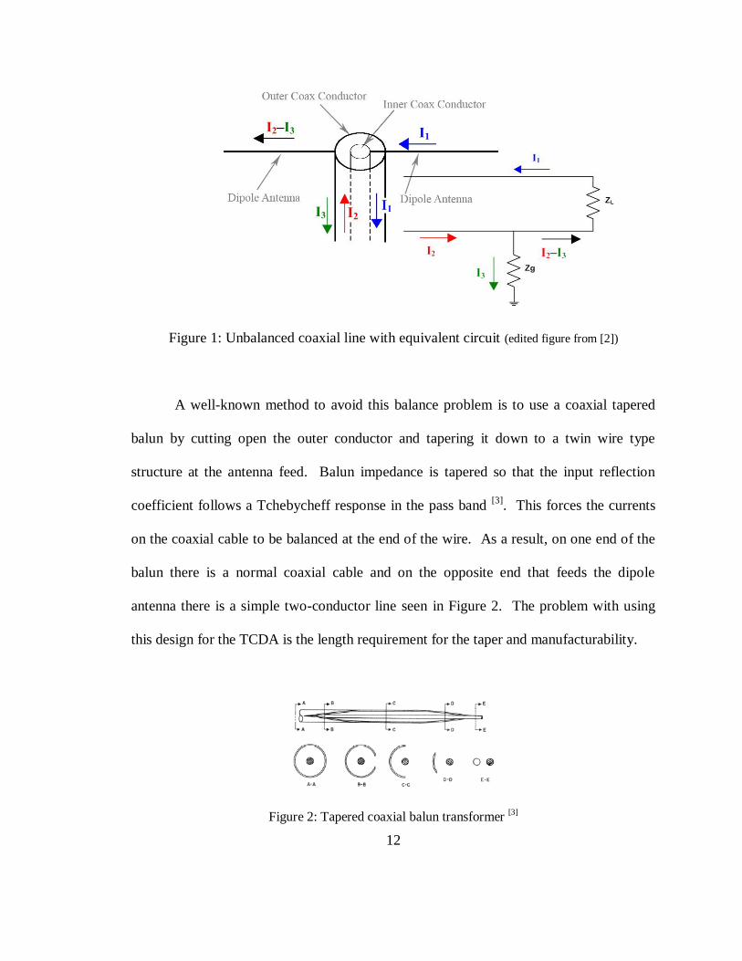
12
Figure 1: Unbalanced coaxial line with equivalent circuit (edited figure from [2])
A well-known method to avoid this balance problem is to use a coaxial tapered
balun by cutting open the outer conductor and tapering it down to a twin wire type
structure at the antenna feed. Balun impedance is tapered so that the input reflection
coefficient follows a Tchebycheff response in the pass band [3]
. This forces the currents
on the coaxial cable to be balanced at the end of the wire. As a result, on one end of the
balun there is a normal coaxial cable and on the opposite end that feeds the dipole
antenna there is a simple two-conductor line seen in Figure 2. The problem with using
this design for the TCDA is the length requirement for the taper and manufacturability.
Figure 2: Tapered coaxial balun transformer [3]

13
1.3. Organization of Thesis
The remainder of this thesis is organized into four parts. Chapter 2 will discuss
the common mode problem associated with feeding a tightly coupled dipole array. The
common mode problem will be examined and a solution, an enclosed feeding system,
will be presented. Chapter 3 presents two wavelength restrictive 180 degree hybrid
designs, the Raytheon tapered hybrid and a simple delay line hybrid. An idea to remedy
the wavelength restrictions of the delay line hybrid is examined in the analysis of the gap
phase reversal hybrid. Chapter 4 presents analysis on an enclosed stripline to twin wire
transition. Research is also presented on a dual enclosed stripline structure that is mated
to the enclosed stripline to twin wire transition in an effort to create a fully enclosed
structure with no wavelength limitations.
CHAPTER 2: TCDA COMMON MODE PROBLEM
2.1. Tightly Coupled Dipole Array
Conventional antenna phased array design usually begins by identifying an
antenna with desirable bandwidth and size and placing the element in an array. Usually a
spacing of
between elements or less is utilized in order to achieve broadside directivity
with 0° phase difference between elements and to avoid grating lobes when scanning [2]
.
However, when the array elements are brought too close to one another, mutual coupling
dominates and often results in diminished antenna performance due to impedance

14
mismatch at the element feed. For the tightly coupled dipole array, the dipole antennas
are brought very close to one another creating a tip to tip capacitance. Dr. Benedikt
Munk discovered that when this array is brought close to a ground plane at about 0.4λ at
the high frequency, the ground plane inductive reactance cancels the array capacitive
reactance for low frequencies. At high frequencies, the ground plane capacitive reactance
cancels the array’s inductive reactance [5]
as a result, the antenna is mostly resistive and
easily achieves a 4:1 bandwidth. Figure 3 illustrates a unit cell model of a single dipole
element over a ground plane as well as a 4x4 element array for L-Band (1GHz – 2GHz).
Figure 3: Unit cell model and 4x4 array of TCDA
The elements in Figure 3 are each individually excited utilizing a lumped port.
Through parametric analysis by means of unit cell modeling in ANSYS/Ansoft HFSS full
Tip Capacitance
0.4*λ at high frequency
Metal Ground Plane
15
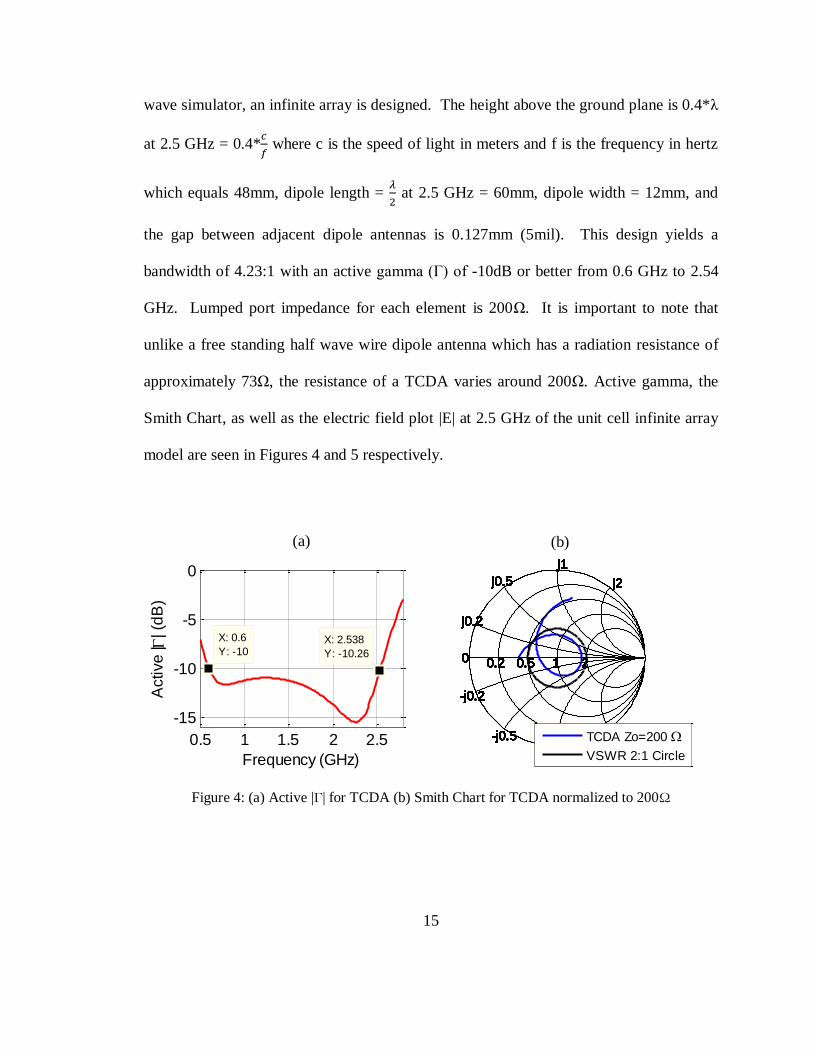
wave simulator, an infinite array is designed. The height above the ground plane is 0.4*λ
at 2.5 GHz = 0.4*
where c is the speed of light in meters and f is the frequency in hertz
which equals 48mm, dipole length =
at 2.5 GHz = 60mm, dipole width = 12mm, and
the gap between adjacent dipole antennas is 0.127mm (5mil). This design yields a
bandwidth of 4.23:1 with an active gamma (Γ) of -10dB or better from 0.6 GHz to 2.54
GHz. Lumped port impedance for each element is 200Ω. It is important to note that
unlike a free standing half wave wire dipole antenna which has a radiation resistance of
approximately 73Ω, the resistance of a TCDA varies around 200Ω. Active gamma, the
Smith Chart, as well as the electric field plot |E| at 2.5 GHz of the unit cell infinite array
model are seen in Figures 4 and 5 respectively.
Figure 4: (a) Active |Γ| for TCDA (b) Smith Chart for TCDA normalized to 200Ω
0.5 1 1.5 2 2.5
-15
-10
-5
0
X: 0.6
Y: -10
Frequency (GHz)
Active
| | (d
B)
X: 2.538
Y: -10.26
j2
j1
j0.5
j0.2
0
-j2
-j1
-j0.5
-j0.2
210.50.2
j2
j1
j0.5
j0.2
0
-j2
-j1
-j0.5
-j0.2
210.50.2
j2
j1
j0.5
j0.2
0
-j2
-j1
-j0.5
-j0.2
210.50.2
j2
j1
j0.5
j0.2
0
-j2
-j1
-j0.5
-j0.2
210.50.2
j2
j1
j0.5
j0.2
0
-j2
-j1
-j0.5
-j0.2
210.50.2
j2
j1
j0.5
j0.2
0
-j2
-j1
-j0.5
-j0.2
210.50.2
j2
j1
j0.5
j0.2
0
-j2
-j1
-j0.5
-j0.2
210.50.2
j2
j1
j0.5
j0.2
0
-j2
-j1
-j0.5
-j0.2
210.50.2
j2
j1
j0.5
j0.2
0
-j2
-j1
-j0.5
-j0.2
210.50.2
j2
j1
j0.5
j0.2
0
-j2
-j1
-j0.5
-j0.2
210.50.2
j2
j1
j0.5
j0.2
0
-j2
-j1
-j0.5
-j0.2
210.50.2
j2
j1
j0.5
j0.2
0
-j2
-j1
-j0.5
-j0.2
210.50.2
j2
j1
j0.5
j0.2
0
-j2
-j1
-j0.5
-j0.2
210.50.2
j2
j1
j0.5
j0.2
0
-j2
-j1
-j0.5
-j0.2
210.50.2
j2
j1
j0.5
j0.2
0
-j2
-j1
-j0.5
-j0.2
210.50.2
j2
j1
j0.5
j0.2
0
-j2
-j1
-j0.5
-j0.2
210.50.2
j2
j1
j0.5
j0.2
0
-j2
-j1
-j0.5
-j0.2
210.50.2
j2
j1
j0.5
j0.2
0
-j2
-j1
-j0.5
-j0.2
210.50.2
j2
j1
j0.5
j0.2
0
-j2
-j1
-j0.5
-j0.2
210.50.2
j2
j1
j0.5
j0.2
0
-j2
-j1
-j0.5
-j0.2
210.50.2
j2
j1
j0.5
j0.2
0
-j2
-j1
-j0.5
-j0.2
210.50.2
j2
j1
j0.5
j0.2
0
-j2
-j1
-j0.5
-j0.2
210.50.2
j2
j1
j0.5
j0.2
0
-j2
-j1
-j0.5
-j0.2
210.50.2
j2
j1
j0.5
j0.2
0
-j2
-j1
-j0.5
-j0.2
210.50.2
j2
j1
j0.5
j0.2
0
-j2
-j1
-j0.5
-j0.2
210.50.2
j2
j1
j0.5
j0.2
0
-j2
-j1
-j0.5
-j0.2
210.50.2
j2
j1
j0.5
j0.2
0
-j2
-j1
-j0.5
-j0.2
210.50.2
j2
j1
j0.5
j0.2
0
-j2
-j1
-j0.5
-j0.2
210.50.2
j2
j1
j0.5
j0.2
0
-j2
-j1
-j0.5
-j0.2
210.50.2
j2
j1
j0.5
j0.2
0
-j2
-j1
-j0.5
-j0.2
210.50.2
j2
j1
j0.5
j0.2
0
-j2
-j1
-j0.5
-j0.2
210.50.2
j2
j1
j0.5
j0.2
0
-j2
-j1
-j0.5
-j0.2
210.50.2
j2
j1
j0.5
j0.2
0
-j2
-j1
-j0.5
-j0.2
210.50.2
j2
j1
j0.5
j0.2
0
-j2
-j1
-j0.5
-j0.2
210.50.2
j2
j1
j0.5
j0.2
0
-j2
-j1
-j0.5
-j0.2
210.50.2
j2
j1
j0.5
j0.2
0
-j2
-j1
-j0.5
-j0.2
210.50.2
j2
j1
j0.5
j0.2
0
-j2
-j1
-j0.5
-j0.2
210.50.2
j2
j1
j0.5
j0.2
0
-j2
-j1
-j0.5
-j0.2
210.50.2
j2
j1
j0.5
j0.2
0
-j2
-j1
-j0.5
-j0.2
210.50.2
j2
j1
j0.5
j0.2
0
-j2
-j1
-j0.5
-j0.2
210.50.2
j2
j1
j0.5
j0.2
0
-j2
-j1
-j0.5
-j0.2
210.50.2
TCDA Zo=200
VSWR 2:1 Circle
(a) (b)

16
Figure 5: Magnitude of E at 2.5 GHz in the x-z plane
It is interesting to observe that we see a radiation source in three locations on the
dipole antenna. One source at the lumped port feed, and on both tips of the dipole where
it couples to the neighboring element. This shows that despite the lack of a physical feed
at the edge of the dipole, it still acts as another radiating source due to mutual coupling of
the active array. Two ideal fictitious methods for feeding the array are discussed in
sections 2.2-2.3 below.
2.2. Twin Wire Feed and Common Mode Problem
As discussed in section 1.2, each dipole antenna is a balanced system and operates
optimally when excited by a balanced feed. Figure 6(a) demonstrates a unit cell
representation of the dipole antenna fed by a twin wire transmission line. The advantage
of exciting each array element with a twin wire feed is that the currents on the twin wires
are exactly 180° out of phase with respect to one another with equal amplitude which
L
W

17
meets the requirements of a balanced system. The twin wire transmission line is excited
by a lumped port just above the ground plane.
Figure 6: (a) Unit cell of twin wire fed dipole (b) Twin wire top view diameter and spacing
Transmission line resistance was calculated to be 200Ω as follows [6]
:
(
) (
)
(
) √
[ ] [ ]
Where µ is the permeability of free space, ε is the permittivity of free space, a is the
radius of the conductor in meters, and D is the center to center spacing of the conductors
in meters. This is illustrated in Figure 6(b).
This would seem to be an ideal method for feeding the antenna, however there is a
fundamental problem with this system. When the length of the dipole arms through the
µ,εArrow denotes current direction a
D
(a) (b)

18
twin wire feed is equivalent to one wavelength, there no longer exists the differential
mode current displayed in Figure 6(a). Rather, there exists a common mode current and
the antenna’s reflection coefficient reaches 1, causing the gain performance to diminish.
This only occurs in the presence of the active array. It is also important to note that this
occurs in an ideal situation, where the phase difference on the wires is precisely 180°,
there is no amplitude unbalance, yet the common mode problem still exists over a narrow
bandwidth. When the phase unbalance at the lumped port feeding the twin wires
increases to 5° and 10°, the common mode issue becomes more profound, and slightly
wider band. Since it is nearly impossible to fabricate a wide band feed that has no phase
or amplitude unbalance over a wide bandwidth, it is important to realize the performance
degradation of the twin wire feeding method with 5° and 10° phase unbalance. The
common mode problem is illustrated in the surface current vector plot in Figure 7(a) at
1.906GHz on the dipole arms and in Figure 7(b) at 1.85GHz, active |Γ| for no phase
unbalance, as well as realized co-polarized and cross-polarized gain is seen in Figure 8(a)
and 8(b) respectively. This common mode problem also becomes worse when the array
is scanned further from broadside. Figure 8(a) shows a spike at 1.906 GHz nearly
reaching an active |Γ| of 0dB, this problem is reflected in the realized gain plot in Figure
8(b)

19
Figure 7: Dipole surface vector current (a) Common mode at 1.906GHz (b) Differential mode at
1.85GHz
Figure 8: (a) Active |Γ| (b) Realized gain co-polarization and cross-polarization
L1
L2
L3
L4
L5
L1+L2+L3+L4+L5 = λ at 1.906GHz
(a) (b)
1 1.5 2 2.5-25
-20
-15
-10
-5
0
Frequency (GHz)
Active
| | (d
B) X: 1.906
Y: -1.574
1.7 1.8 1.9 2 2.1
-60
-40
-20
0
Frequency (GHz)
Re
alize
d G
ain
(d
B)
X: 1.906
Y: -19.35
Co-Pol
Cross-Pol

20
2.3. Dual Coaxial Balanced Feed
There are multiple different ways to suppress the common mode problem. One
can design the array to simply make each element slightly shorter than
at the high
frequency to push this common mode problem out of the band of operation. However the
consequence of this is a greater number of elements per unit area than would have existed
otherwise. This has cost implications, not only driving the manufacturing costs of the
array up due to extra elements, but more importantly each extra element requires
excitation by another transmit/receive module which is expensive. Another method is to
use shorting pins close to the feed from each dipole arm to ground to suppress the
common mode. The issues with this design is ease of manufacturability, and the
introduction of a loop mode that will exist between adjacent array element shorting pins
that needs to be controlled/suppressed as well as scan performance limitations.
Ideally a method of feeding that would allow for optimal length for the dipoles,
and suppress the common mode without adding any extra complications would be a
completely enclosed feeding system. An enclosed structure meaning the entire feed is
contained in a metal structure that is unable to radiate and shielded from external forces.
The simplest form of this balanced system are two coaxial cables fed 180° out of phase
with each outer conductor soldered to one another to cancel any currents that might flow
on the outer conductor. This type of feed is displayed in Figure 9 below.

21
Figure 9: Dual coaxial balanced feed
Each coaxial cable is excited by a wave port right above the ground plane. The
outer cylinder is an air “substrate” covered in PEC (Perfect Electric Conductor) on the
perimeter but made transparent for ease of illustration. Air was chosen as the material
between the conductors in order to keep any existence of a common mode problem at
approximately the same frequency as the twin wire case. The impedance of the coaxial
cables are 100Ω each, at the feed of the antenna the center conductors add in series giving
a 200Ω impedance. Active |Γ| for the unit cell infinite array simulation of the coaxial
feed in Figure 9 is shown in Figure 10.
Figure 10: Coaxial feed (a) Active |Γ| (b) Realized gain co-polarization and cross-polarization
L1
L2
L3
L4
L5
L1+L2+L3+L4+L5 = λ at 1.906GHz
1 1.5 2 2.5-15
-10
-5
0
Frequency (GHz)
Active
| | (d
B)
(a)
1.7 1.8 1.9 2 2.1
-100
-50
0
Frequency (GHz)
Re
alize
d G
ain
(d
B) (b)
Co-Pol
Cross-Pol

22
Active |Γ| is different from the twin wire case because the array has not been
optimized for this feed structure. Figure 10 as well as the vector surface current plot
from Figure 9 shows no common mode problem as seen in Figure 8. As a result the
remainder of the focus of this paper will concentrate on a feeding structure that will be
enclosed, fit in small physical dimensions (unit cell), and be capable of operating in a
dual polarization configuration. An ideal stripline based illustration of this full system
concept is seen in Figure 11 and Figure 12.
Each antenna would be fed by 50Ω coaxial cables directly connected to enclosed
stripline, these lines would need to split into two enclosed stripline structures and
eventually feed the antenna as shown in Figure 11. Figure 12 shows a front view and top
view of the coaxial fed enclosed stripline and 4 port enclosed stripline feed respectively.
Figure 11: 4 port enclosed unit cell ideal feeding system
Set of two 50 Ω Coax Fed Enclosed Stripline
4 Port enclosed stripline to feed cross-dipole antennas (Unit cell)
Port 3: 0
To feed antenna 1
To feed antenna 2
Enclosed/shielded 180 degree hybrid balun
100 ΩEnclosedStripline
Antenna 1
Antenna 2
Enclosed/shielded 180 degree hybrid balun
Port 1: 0
Port 2: 180
Port 4: 180

23
Figure 12: (a) Front view of coax feed from Figure 11 (b) Top view of dipole antenna feed
CHAPTER 3: WAVELENGTH BASED HYBRID AND GAP HYBRID
3.1. Raytheon Tapered Hybrid
Defense contractor Raytheon has an old patent on a three port coaxial fed 180°
hybrid based on a tapered microstrip line. This concept was used to create the structure
in Figure 13.
Figure 13: Raytheon based 180° hybrid
(b) Top View
Substrate
Trace
Coax Center Conductor
Coax Outer Conductor
EnclosedStriplineWall
Port 1
Port 2
Port 3
Port 4
(a) Front View
λ/2 at lowest frequency (2GHz)
60mm
Port1
Port 2 Port 3
50Ω100Ω

24
The model was built and simulated in CST Studio Suite 2009. This hybrid
operates by taking the microstrip trace on one of the 100Ω lines and tapering it out to
become the new “ground” plane. Likewise, the ground plane is tapered down to become
the microstrip trace. As a result, if a coaxial cable were connected to the ports, it would
be connected to port 3 opposite in comparison to port 2. This is easily seen by observing
the direction of the wave ports in Figure 13, Port 2 would have the center conductor of
the coaxial cable on the top of the board where Port 3 would have the center conductor on
the bottom side of the printed circuit board. S-Parameter magnitude and phase is shown
in Figure 14 (a) and (b).
Figure 14: Raytheon Tapered Hybrid S-Parameters (a) Magnitude (b) Phase
It is seen in Figure 14(a) that there is an amplitude unbalance between ports 2 and
3. At some places this unbalanced ripple is as much as 7dB, with |S21| and |S31| often
worse than -4dB which is unacceptable. The phase in Figure 14(b) is relatively adequate.
0 5 10 15 20-20
-15
-10
-5
0
Frequency (GHz)
Ma
gn
itu
de
(d
B)
(a)
|S11|
|S21|
|S31|
0 5 10 15 20-200
-100
0
100
200
Frequency (GHz)
S-P
ara
me
ters
(D
eg
ree
s)
(b)
Phase of S21
Phase of S31
25
At the low frequencies the phase reversal is ~173°, and at the highest frequencies ~100°.
This system could be optimized with a more intelligent taper from 5GHz to 15GHz
easily, but the half wave restriction makes it too big. It is difficult to determine how to
enclose this structure and mate it with an enclosed stripline transmission line. As a result
the Raytheon based tapered hybrid will not be useful for the required application.
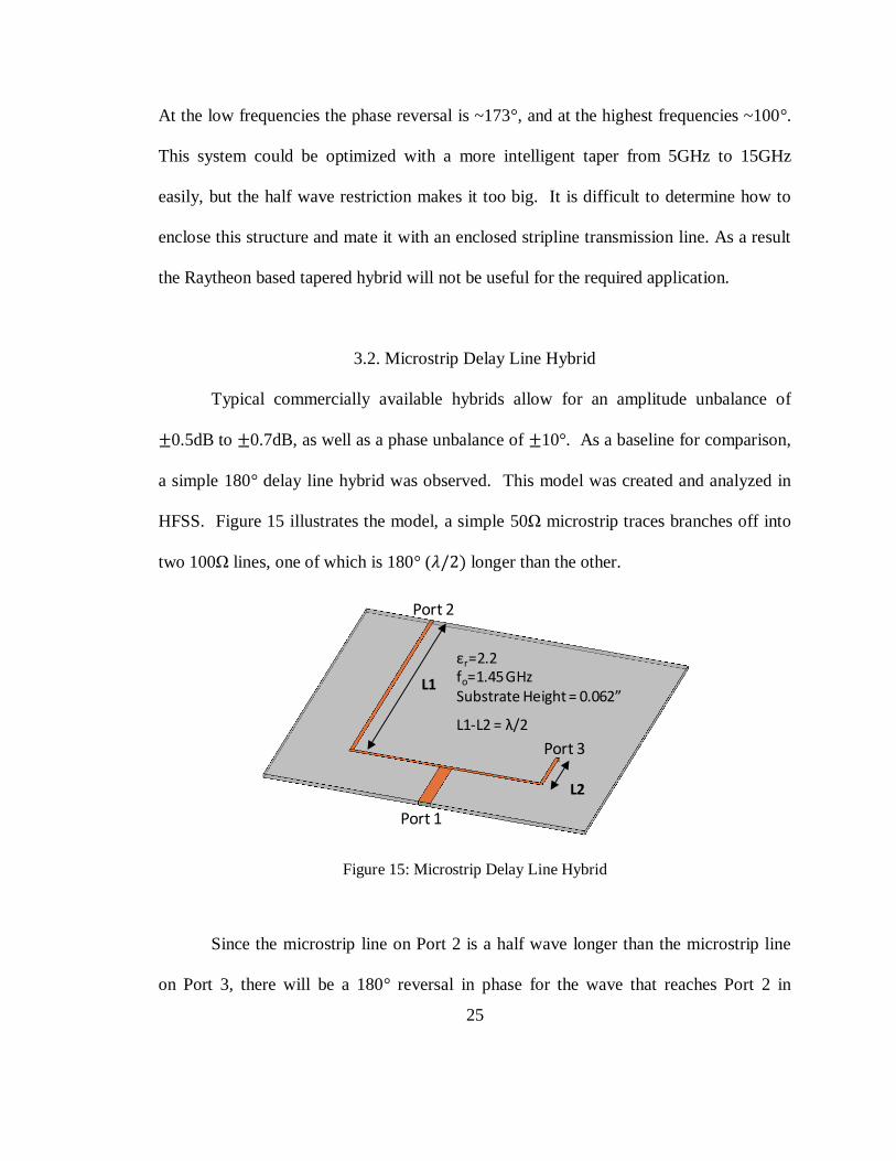
3.2. Microstrip Delay Line Hybrid
Typical commercially available hybrids allow for an amplitude unbalance of
0.5dB to 0.7dB, as well as a phase unbalance of 10°. As a baseline for comparison,
a simple 180° delay line hybrid was observed. This model was created and analyzed in
HFSS. Figure 15 illustrates the model, a simple 50Ω microstrip traces branches off into
two 100Ω lines, one of which is 180° ( longer than the other.
Figure 15: Microstrip Delay Line Hybrid
Since the microstrip line on Port 2 is a half wave longer than the microstrip line
on Port 3, there will be a 180° reversal in phase for the wave that reaches Port 2 in
L1
L2
Port 1
Port 2
Port 3
εr=2.2fo=1.45 GHzSubstrate Height = 0.062”
L1-L2 = λ/2
26
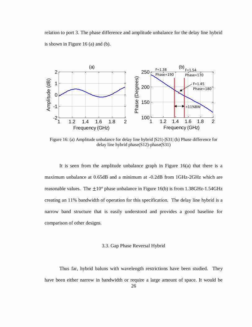
relation to port 3. The phase difference and amplitude unbalance for the delay line hybrid
is shown in Figure 16 (a) and (b).
Figure 16: (a) Amplitude unbalance for delay line hybrid |S21|-|S31| (b) Phase difference for delay line hybrid phase(S12)-phase(S31)
It is seen from the amplitude unbalance graph in Figure 16(a) that there is a
maximum unbalance at 0.65dB and a minimum at -0.2dB from 1GHz-2GHz which are
reasonable values. The 10° phase unbalance in Figure 16(b) is from 1.38GHz-1.54GHz
creating an 11% bandwidth of operation for this specification. The delay line hybrid is a
narrow band structure that is easily understood and provides a good baseline for
comparison of other designs.
3.3. Gap Phase Reversal Hybrid
Thus far, hybrid baluns with wavelength restrictions have been studied. They
have been either narrow in bandwidth or require a large amount of space. It would be
1 1.2 1.4 1.6 1.8 2-2
-1
0
1
2
Frequency (GHz)
Am
plitu
de
(d
B)
(a)
1 1.2 1.4 1.6 1.8 2100
150
200
250
Frequency (GHz)
Ph
ase
(D
eg
ree
s)
(b)F=1.38Phase=190
F=1.54Phase=170
F=1.45Phase=180
≈11%BW

27
more ideal to consider a way to reverse the phase of one of the ports of a 3 port structure
without the reliance of a wavelength restrictive. One such structure would be a gap phase
reversal hybrid, the concept behind the phase reversal is seen in the cross-sectional view
in Figure 17.
Figure 17: Gap phase reversal concept with E-field vectors
The red arrows represent the electric field lines between the ground plane and
microstrip trace. The idea would be to introduce a small gap in the microstrip trace, this
would allow fringing fields to occur where the gap exists and force a reversal in phase for
the electric fields from one side of the trace to the other. Many commercial 180° hybrids
are only useful for specific frequency ranges due to wavelength restrictive designs. If the
gap phase reversal occurs as expected, then a perfect 180° phase difference would occur
that was not frequency dependent, and thus would be an ultra-wide bandwidth device.
The HFSS model and simulation results are seen in Figure 18 and Figure 19 respectively.
The hybrid is very similar to that of the delay line hybrid in Figure 15, however all trace
lengths are identical, and one trace has a 10mil gap. Simulations were run from 1GHz-
2GHz.
Microstrip Side ViewMicrostrip Trace
Ground

28
Figure 18: Gap phase reversal hybrid
Figure 19: Gap phase reversal hybrid (a) Surface current plot (b) S-Parameter magnitude
Figure 19 shows a problem with this initial design. At 1.09GHz it is seen that
|S31| drop significantly. This is due to the fact that the 10mil gap is too large for any
power transfer to the other side of the microstrip line. As a result, it appears to the
system as an open circuit. Figure 18 shows that the length from the gap to the center of
Gap=10mil
4L
at 1.09 GHz
εr=2.2Substrate Height = 0.062”
Port 2 Port 3
Port 1
Jsurf Plot2 GHz
1 1.2 1.4 1.6 1.8 2-40
-30
-20
-10
0
Frequency (GHz)
Ma
gn
itu
de
(d
B)
(b)
|S11|
|S21|
|S31|1.09GHz
(a)

29
the trace connected to Port 1 is a quarter wavelength, which transforms this open circuit
to a short circuit which accounts for the significant drop at 1.09GHz. The surface current
plot in Figure 19(a) shows visually that there is little energy traveling on the trace after
the gap. To determine the substrate height and gap width that was necessary for current
to transfer across the gap, a parametric study was conducted on a single microstrip trace.
The model is displayed in Figure 20 with and without a gap. The gap was varied from
10mil to 0.1mil with a substrate height of 1mm, dielectric constant of 2.2 (lossless), and
microstrip trace impedance of 95Ω (1mm width).
Figure 20: Microstrip with (a) No gap (b) 0.1mil gap
Figure 21 shows the |S-Parameters| for the no gap, 10mil, 5mil, 1mil, and 0.1mil
gap cases. Figure 22 compares the phase of S21 for each of these cases. This was
simulated in CST Studio Suite 2009, thus a comparison of the time domain pulse is
observed in Figure 23 between the no gap and the 0.1 mil gap cases.
(a) (b)
Port 1
Port 2

30
Figure 21: (a) |S11| Comparison (b) |S21| Comparison
Figure 22: Phase of S21 Comparison
Figure 23: Time domain pulse (a) No gap (b) 0.1mil gap
0 2 4 6 8 10 12 14 16 18
-40
-20
0
Frequency (GHz)
|S1
1| (d
B)
(a)
10mil Gap
5mil Gap
1mil Gap
0.1mil Gap
No Gap
0 2 4 6 8 10 12 14 16 18-20
-10
0
Frequency (GHz)
|S2
1| (d
B)
(b)
10mil Gap
5mil Gap
1mil Gap
0.1mil Gap
No Gap
0 2 4 6 8 10 12 14 16 18-200
-100
0
100
200
Frequency (GHz)
Ph
ase
(D
eg
ree
s)
10mil Gap
5mil Gap
1mil Gap
0.1mil Gap
No GapNo 180deg
Phase Reversal
0 0.1 0.2 0.3
0
0.2
0.4
0.6
0.8
1
Time (ns)
Am
plitu
de
(a)
Input Signal
Output 11
Output 21
0 0.1 0.2 0.3 0.4-0.2
0
0.2
0.4
0.6
0.8
Time (ns)
Am
plitu
de
(b)
Input Signal
Output 11
Output 21

31
In Figure 21(a), we see that |S11| is only acceptable (-10dB or better) for the
0.1mil gap case and naturally the no gap case. The same is seen in the |S21| response in
Figure 21(b), there is poor power transfer for the 10mil, 5mil, and 1mil cases. Despite
significantly better power transfer for the 0.1mil case past 2GHz, there is no phase
reversal which is observed in Figure 22. Looking at the time domain pulse of the no gap
and 0.1mil gap cases in Figure 23 confirms what is seen in Figure 23, the peak of the
output 21 signal drops to 0.8 denoting a reflection which is seen in the output 11 signal.
For a 180° phase reversal, the peak of the output 21 signal would ideally need to reach -1
if the input signal were 1.
In order to have reasonable |S21| transfer, the gap must be incredibly small,
~0.1mil, the human hair is 3.3mil in diameter for comparison. The gap is small enough
that the fields simply jump over it and do not “see” the gap. It is important to note that
typically the smallest size gap that could realistically be milled out of a microstrip trace is
on the order of 3mil-5mil, making a 0.1mil gap nearly impossible to fabricate. Despite
the small size for the gap, there still is no phase reversal, thus it is concluded that the
180° gap hybrid will not work for this application.
Chapter 4 will begin study of a different frequency non-dependent method for
creating the 180° hybrid balun. Ultimately a structure that starts as enclosed stripline will
transition into a twinwire transmission line and branch off into two dual enclosed
striplines that would feed the antenna. Analysis of this structure will be separated into
two portions; the enclosed stripline to twin wire, then the twin wire to dual enclosed
stripline. Additionally, this paper will discuss the mating of the two together.

32
CHAPTER 4: ENCLOSED STRIPLINE TO DUAL ENCLOSED STRIPLINE 180°
HYBRID
4.1. Enclosed Stripline to Twin Wire Analysis
Traditional stripline transmission lines consist of a metal trace sandwiched in a
substrate between parallel plates above and below the trace. The parallel plates extend for
a significant distance when compared to the width of the trace perpendicular to the
direction the trace is fabricated in and have the same length running parallel to the trace.
The big advantage of the stripline for the required application is that it is a TEM
(transverse electromagnetic) transmission line, much like a coaxial cable. As a result it is
“non-dispersive”, enclosed, and should have no cutoff frequency. The disadvantage is
that they are slightly more difficult to fabricate and costly since they require the use of
two PCB boards. Another item to note, because the trace is entirely enclosed in a
substrate, trace widths are smaller when compared to microstrip since fringing fields are
entirely captured in the substrate rather than partially in air and partially in a substrate as
in the case of microstrip. This can be an advantage if a small size is required, but a
disadvantage if the trace widths become small enough to cause fabrication problems.
Traditional stripline impedance can be calculated with the following simplified
equation[6]
:
√ [
( )
] [ ]
A cross-sectional view of a stripline transmission line is depicted in Figure 24.

33
Figure 24: Cross-Sectional view of stripline
The enclosed stripline used for the purpose of this paper would include the
vertical lines in Figure 24 thus creating a square wave guide with a trace embedded in the
middle. Traditional stripline governed by Equation 2 would not include these vertical
lines. It was found that the impedance of the stripline in Figure 24 with the vertical lines
was roughly 84.4% of Equation 2.
Two versions of the stripline to twin wire transition are seen in Figure 25.
Dimensions listed in the figure are congruent with those displayed in Figure 6(b) and
Figure 24. The first is a 50Ω system, and the second is 100Ω. The stripline is excited
with a waveport in CST Studio Suite 2009 (this software is used for the remainder of this
paper), and a waveport is placed on the end of the twin wire transmission lines. These
ports and the PEC walls of the enclosed stripline are made invisible to better illustrate the
structure. The stripline impedance was calculated using 84.4% of Equation 2, and the
twin wire impedance was calculated using Equation 1. One of the twin wire lines goes
through a circular cut in the top of the PEC sheet of the stripline waveguide, and connects
to the stripline trace. The other twin wire line connects to the top stripline wall. The idea
is to force the current of the trace onto one twin wire, then the current from the stripline
H
εrW
t
H

34
box onto the other twin wire. This would create a differential mode on the wires and
result in a balanced twin wire at port 2. S-Parameter results for each model are displayed
in Figure 26(a) and Figure (b).
Figure 25: Enclosed stripline to twin wire (a) 50Ω W=0.24mm H=0.6096mm a=0.28mm
D=0.305mm (b) 100Ω W=0.07mm H=0.6096mm a=0.225mm D=0.305mm
Figure 26: S-Parameters (a) 50Ω system (b) 100Ω system
Port 1
Port 2
Twin Wire 50Ω
Enclosed Stripline 50Ω
Er=3.38
Enclosed Stripline100Ω
Port 2
Twin Wire 100Ω
Port 1Er=3.38
(a) (b)
0 5 10 15 20-30
-20
-10
0
Frequency (GHz)
Ma
gn
itu
de
(d
B)
(a)
|S11|
|S21|
0 5 10 15 20-30
-20
-10
0
Frequency (GHz)
Ma
gn
itu
de
(d
B)
(b)
|S11|
|S21|
35
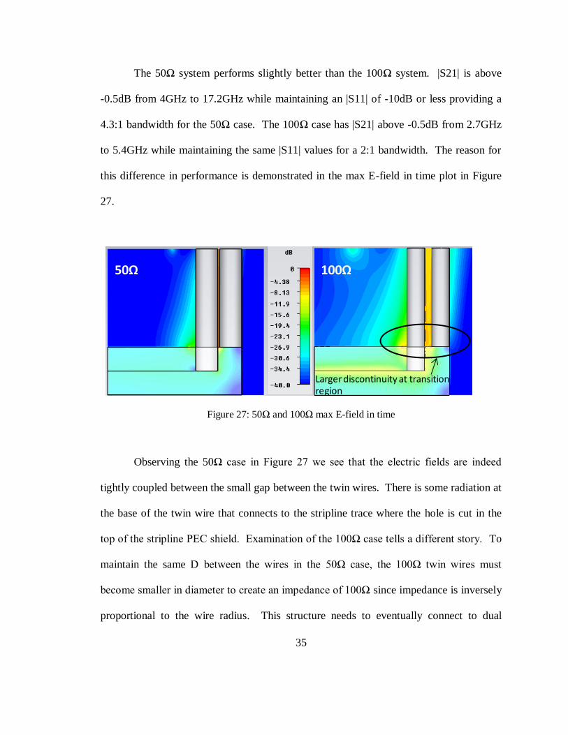
The 50Ω system performs slightly better than the 100Ω system. |S21| is above
-0.5dB from 4GHz to 17.2GHz while maintaining an |S11| of -10dB or less providing a
4.3:1 bandwidth for the 50Ω case. The 100Ω case has |S21| above -0.5dB from 2.7GHz
to 5.4GHz while maintaining the same |S11| values for a 2:1 bandwidth. The reason for
this difference in performance is demonstrated in the max E-field in time plot in Figure
27.
Figure 27: 50Ω and 100Ω max E-field in time
Observing the 50Ω case in Figure 27 we see that the electric fields are indeed
tightly coupled between the small gap between the twin wires. There is some radiation at
the base of the twin wire that connects to the stripline trace where the hole is cut in the
top of the stripline PEC shield. Examination of the 100Ω case tells a different story. To
maintain the same D between the wires in the 50Ω case, the 100Ω twin wires must
become smaller in diameter to create an impedance of 100Ω since impedance is inversely
proportional to the wire radius. This structure needs to eventually connect to dual
Larger discontinuity at transition region
50Ω 100Ω

36
enclosed stripline, thus D must be set such that the twin wires sit at approximately the
center of the dual enclosed stripline traces. Since the twin wires in the 100Ω case allow
for a greater gap between the inner edges of the wires, the electric fields are not as tightly
coupled, as a result we see a greater discontinuity at the stripline to twin wire transition
when compared to the 50Ω case. The S-Parameter plots in Figure 26 do not give us a
feeling for the amplitude or phase unbalance of this system. Section 4.2 will further
investigate quantifying this unbalance.
4.2. Quantifying Phase and Amplitude Unbalance of a Twin Wire Transmission Line
In order to quantify the phase and amplitude unbalance of the system in Figure
25, one would need 3 ports, 1 at the input of the stripline, and two at the end of the twin
wire transmission line. CST will not allow two wave ports to share the same
perpendicular plane and requires at least 1 mesh cell separation between ports. To
separate the E-fields between the twin wires and allow for a 3 port system, a small PEC
divider is placed between the wires. This is seen in the twin wire system in Figure 28.
Figure 28: Twin wire with 3 ports and PEC divider a=0.183mm D=0.5mm H=2mm Zo=100Ω
D
H
Port 1
Port 2
Port 3

37
Another requirement of CST is to have the exact same material within a distance
of 3 mesh cells in either direction of a wave port, thus the height of the metal plate is
made to be 3 mesh cells. The width of the metal plate was varied to X% blockage
between the wires and analyzed in Figure 29.
Figure 29: Twin wire 3 port analysis for different percentages of blockage (a) |S21| (b) S21 phase
unbalance (c) |S11|
In Figure 29(a) only |S21| is plotted because |S31| is equivalent to |S21|. The twin
wire transmission line is inherently ultra-wide band in nature and should not have a low
frequency cutoff, the reason for the low frequency cutoff observed in 29(a) and 29(c) is
0 2 4 6 8 10 12 14-5
-4
-3
-2
-1
0
Frequency (GHz)
Ma
gn
itu
de
(d
B)
(a)
50% Blockage
20% Blockage
1% Blockage
0 2 4 6 8 10 12 14178
179
180
181
182
Frequency (GHz)P
ha
se
Un
ba
lan
ce
(D
eg
) (b)
50% Blockage
1% Blockage
0 2 4 6 8 10 12 14-40
-30
-20
-10
0
Frequency (GHz)
Ma
gn
itu
de
(d
B)
(c)
50% Blockage
40% Blockage
30% Blockage
20% Blockage
10% Blockage
5% Blockage
1% Blockage
0% Blockage

38
because the low frequency energy in the system did not die out completely. This is a
problem because CST is a FDTD (Finite-Difference Time-Domain) simulation program,
and would be remedied by letting the simulation run longer. The metal plate has little
significant effect on |S21| or phase unbalance seen in 39(a) and 39(b) even at 50%
blockage (phase unbalance for both cases nearly overlap). However, |S11| is affected; the
best balance between simulation time and reasonable |S11| was determined to be 20%
blockage. The simulation time step on CST is dictated by the smallest feature (i.e. mesh
cell), a smaller percentage of blockage relates to a smaller simulation feature which
means an increase in simulation time which is why 20% blockage was chosen as it yields
an acceptable |S11| of -20dB to simulation time tradeoff. This three port analysis was
applied to the models in Figure 25, new models and results are in Figures 30-32.
Figure 30: Enclosed stripline to twin wire 3 port analysis (a) 50Ω (b) 100Ω
Port 1
Port 2
Port 3
100Ω
Port 2
Port 3
Port 1
50Ω
(a) (b)

39
Figure 31: Enclosed stripline to twin wire 3 port |S-Parameters| (a) 100Ω (b) 50Ω
Figure 32: Enclosed stripline to twin wire 3 port phase unbalance (S21-S31)
With the three port analysis of the enclosed stripline to twin wire, we can now
quantify the amplitude and phase unbalance. Ideally |S21| = |S31| = -3dB for the S-
parameters seen in Figure 31. For the 50Ω case, |S21| is approximately -3dB as expected,
however |S31| varies from -3.5dB to -4.2dB over 2GHz to 18GHz, this 0.5dB to 0.7dB
unbalance is comparable to the unbalance seen in commercially available hybrids. As
seen earlier, the 100Ω transmission lines are worse, |S21| is the expected -3dB for the
0 2 4 6 8 1012 1416 18 20-20
-15
-10
-5
0
Frequency (GHz)
Ma
gn
itu
de
(d
B)
(a)
|S21|
|S31|
|S11|
0 2 4 6 8 1012 1416 18 20-20
-15
-10
-5
0
Frequency (GHz)
Ma
gn
itu
de
(d
B)
(b)
|S21|
|S31|
|S11|
0 2 4 6 8 10 12 14 16 18 20160
170
180
190
200
Frequency (GHz)
Ph
ase
Un
ba
lan
ce
(D
eg
)
Phase Unbalance 100
Phase Unbalance 50

40
majority of the band, |S31| varies from -5dB to -5.4dB from 3GHz to 18GHz. |S11| is
-10dB or better over these frequencies for both cases, thus this lower value for |S31| is not
due to a miss-match, and it is not due to any conductor/material losses as the model is
loss-less. The lower |S31| is due to radiation from the wires at the transition region seen
in Figure 27. It is easy to see that there is far more radiation for the 100Ω case as
compared to the 50Ω case which accounts for the lowered |S31| values. Phase values in
Figure 32 for both cases are acceptable.
Part of the problem with this design is that the current from the enclosed stripline
is not equally distributed to the twin wire transmission lines. The stripline trace is
directly connected to the left most twin wire in Figure 30, essentially all the current from
that trace is transferred to the twin wire. However the right most twin wire does not
connect to the entire PEC stripline box, thus it does not receive all the current from the
outer shield of the stripline structure. Further, the hole that is cut for the left most twin
wire creates a disruption in the currents flowing on the stripline PEC box, some is
reflected back to the feed, and some travels around the hole onto the right most twin wire.
In short, with this present design, all the current flowing on the stripline PEC box are not
forced onto the right most twin wire, there is radiation from the stripline to twin wire
transition region causing an amplitude imbalance.

41
4.3. Twin Wire to Dual Enclosed Stripline Analysis
As mentioned earlier, the configuration in section 4.1 and 4.2 will connect to a
dual enclosed stripline structure. The dual enclosed stripline would ultimately become
the feeding transmission lines for a single antenna as described in Figure 11. Due to
fabrication limitations, an enclosed stripline transmission line could not be built like that
shown in Figure 25. Commercially available printed circuit boards contain a substrate
with a dielectric constant, with a sheet of copper rolled or deposited onto both sides of the
board, and then the metal is milled or etched to create the microwave circuitry. As a
result, it would not be feasible to have the metal walls perpendicular to the trace in Figure
25. To relieve this problem, one could create a wall of vias through the multi-layered
board that make up the stripline transmission line. Such an enclosed stripline is depicted
in Figure 33. Generally the smallest fabricatable diameter size for a via is 5mil with a
placement error of no less than 3mil.
Port 1 Port 3
Port 4 Port 2
Figure 33: Dual enclosed via stripline - with and without ground planes

42
Figure 33 shows the dual enclosed stripline, all simulation models displayed
through the rest of this paper will have invisible ground planes for illustrative purposes,
simulations were run with ground planes. Vertical plates that continue from the vias are
left in the model in order to create a proper wave port. Figures 34-35 display the models
and results for enclosed via stripline with 3 vias and 26 vias, 0.47*λ and 0.02* λ at
20GHz respectively.
Figure 34: Dual enclosed via stripline (a) 0.47*λ via spacing model (b) 0.02* λ via spacing (c)
0.47* λ via spacing max surface current (d) 0.02* λ via spacing max surface current
Figure 35: Dual enclosed via stripline |S-Parameters| (a) 0.47*λ (b) 0.02*λ
0 5 10 15 20-60
-40
-20
0
Frequency (GHz)
Ma
gn
itu
de
(d
B)
(a)
|S11|
|S21|
|S31|
|S41|
0 5 10 15 20-60
-40
-20
0
Frequency (GHz)
Ma
gn
itu
de
(d
B)
(b)
|S11|
|S21|
|S31|
|S41|
(a) (b)
(c) (d)
4 2
3 1
3
2 4
1

43
Figure 35 shows that although there is better isolation between port 3 from port 1,
and improved |S11|, |S41| becomes worse. The max surface current plots in Figure 34 (c)
and (d) visually shows that there is slightly more energy at the end of port 4 in the case of
more vias. One of the difficulties with the via walls versus an actual conducting plate is
that the conducting plate is continuous and thus can carry energy much more efficiently.
To overcome the limitation of the via walls, and to ensure good isolation between ports 1-
2 from ports 3-4, a metal strip is added in the same plane as the stripline strip to short the
vias together and make them more continuous. The adjusted model is seen in Figure 36,
with simulated data in Figure 37, Figure 35(b) has been copied into Figure 37 for ease of
comparison.
Figure 36: 0.47*λ via spacing with via shorting strip
In Figure 37 we see that all of the S-Parameters improve by adding the shorting
strip. Figure 37(c) shows a good improvement in |S21| as well, |S21| of the model in
Figure 34(a) varied from -0.4dB to 0dB for comparison.
With Via Strip
1
2
3
4

44
Figure 37: Via enclosed stripline 0.02*λ (a) With shorting strip (b) without shorting strip (c) |S21|
compared
Now that the dual enclosed via stripline have been optimized, a twin wire
transmission line will be introduced. Ideally the twin wires should have spacing D such
that they line up with the center to center spacing of the conducting stripline traces.
However, we need the twin wire inner surface distance to be as small as possible as
0 5 10 15 20-60
-40
-20
0
Frequency (GHz)
Ma
gn
itu
de
(d
B)
(a)
|S11|
|S21|
|S31|
|S41|
0 5 10 15 20-60
-40
-20
0
Frequency (GHz)
Ma
gn
itu
de
(d
B)
(b)
|S11|
|S21|
|S31|
|S41|
0 5 10 15 20-0.5
-0.4
-0.3
-0.2
-0.1
0
Frequency (GHz)
Ma
gn
itu
de
(d
B)
(c)
|S21| without strip
|S21| with strip

45
learned in the 50Ω and 100Ω cases from section 4.1. Models of the twin wire to enclosed
via stripline are shown in Figure 38 with results in Figure 39.
Figure 38: Twin wire to dual enclosed via stripline 100Ω (a) Twin wire D=0.416mm (b) Twin
wire D=0.213mm
Figure 39: Twin wire to dual enclosed via stripline 100Ω |S-parameters| (a) Twin wire
D=0.416mm (b) Twin wire D=0.213mm
Figure 38(a) and results in Figure 39(a) shows the 100Ω twin wire centered on the
stripline. |S31| is not displayed in Figure 39 since it is identical to |S21|. |S21| is greater
than or equal to -3.5dB from 4.3GHz to 11GHz. Figure 38(b) and Figure 39(b) shows
0 5 10 15 20 25-30
-20
-10
0
Frequency (GHz)
Ma
gn
itu
de
(d
B)
(a)
|S11|
|S21|
0 5 10 15 20 25-30
-20
-10
0
Frequency (GHz)
Ma
gn
itu
de
(d
B)
(b)
|S11|
|S21|
Port 1: 100Ω
Port 2: 50Ω Port 3: 50Ω
(a) (b)
46
another 100Ω configuration where the twin wires are brought closer to one another in
order to make it possible to connect them to the structure in Figure 25. |S21| is greater
than or equal to -3.5dB from 5.2GHz to 21GHz. The configuration in 38(b) is wider in
bandwidth and operates at a higher frequency because the wires are closer to one another.
Since the wires are closer, and the rectangular cut in the box is larger in proportion to
their spacing, there is better transfer of the electric fields from one wire to the other.
Thus it becomes necessary to ensure the hole cut in the ground plane is optimized in
width and length to enable optimal twin wire performance.
Only a 100Ω configuration is shown for a couple of different reasons. Although
we learned that the 50Ω system performs better for the enclosed stripline to twin wire
transition from Figure 25, the TCDA naturally operates around 200Ω and would be easier
to re-design to operate at 100Ω rather than 50Ω. Also, the 50Ω twin wire would be split
into two 25Ω enclosed stripline traces rather than 50Ω. The consequence of this are
traces that are much wider and it is no longer possible to have a square shaped enclosed
stripline structure, rather there would need to be a rectangular shaped enclosed stripline
forcing longer tabs as those seen on Figure 38 (b). The problem with longer tabs is that
the junction seen at the terminals of the twin wire transmission lines is seen by the
striplines as a parallel circuit, and thus would be 50Ω||50Ω = 25Ω much like the
microstrip traces in Figure 15 where 100Ω||100Ω=50Ω, not 100Ω which is the
characteristic impedance of the twin wires. The configuration in Figure 38(a) allows the
twin wire impedance to be split as a series circuit, not a parallel circuit. As a result
having longer tabs creates two sets of transmission lines that see the feed of the twin
47
wires oppositely. The reason a 200Ω system is not analyzed is due to inner surfaces of
the twin wire being farther apart from one another amplifying the twin wire radiation
problem seen in the 100Ω case in Figure 27 when transitioning from stripline to twin
wire.
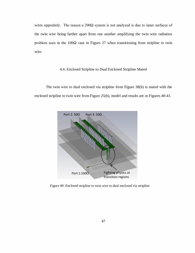
4.4. Enclosed Stripline to Dual Enclosed Stripline Mated
The twin wire to dual enclosed via stripline from Figure 38(b) is mated with the
enclosed stripline to twin wire from Figure 25(b), model and results are in Figures 40-41.
Port 1:100Ω
Port 2: 50Ω Port 3: 50Ω
Fighting physics at transition regions
Figure 40: Enclosed stripline to twin wire to dual enclosed via stripline

48
Figure 41: Enclosed stripline to twin wire to dual enclosed via stripline |S-parameters|
Unfortunately the S-parameters in Figure 41 are not adequate. In short, there is a
huge amplitude unbalance between Port 2 and Port 3. There is little current flowing onto
the right most twin wire accounting for the limited power transfer at Port 3. Also, |S11| is
poor due to the transition region circled in Figure 40. The inner surface of the twin wires
need to be as close as possible to one another, however, the enclosed stripline from ports
2 and 3 have the problem described above when tabs are added at the twin wire feed, and
the traces can only be so close to one another. The inner surface distance (gap) of the
twin wires from Figure 40 and Figure 38(b) is 12 mil, 16 mil gap is observed in Figure
38(a), the gap for the 50Ω and 100Ω cases from Figure 25 are 1mil and 3mil respectively.
This means that the unbalance/radiation problem observed in Figure 27 will be worse in
Figure 40 due to the larger gap. Regrettably, this non-wavelength restrictive system will
not provide the performance required to feed the TCDA.
0 5 10 15 20 25-20
-15
-10
-5
0
Frequency (GHz)M
ag
nitu
de
(d
B)
|S11|
|S21|
|S31|

49
CHAPTER 5: CONCLUSION AND FUTURE WORK
Several different 180° hybrid balun structures are analyzed in this paper. For the
unit cell applications of the tightly coupled dipole array, it is ideal to have a non-
wavelength restrictive structure. The Raytheon hybrid could provide the required
performance however it is to large due to the half wave restriction. The simple delay line
hybrid provides a good narrow band and easy to understand basis for analysis and
performance to compare other hybrids to. The gap hybrid would be a good wavelength
non-restrictive structure, however in order to have sufficient power transfer through the
microstrip trace gap, an un-realizable small gap must be fabricated. Further, there is no
180° phase reversal between the output ports of the gap hybrid. The full enclosed
stripline to twin wire to dual enclosed via stripline looks promising when analyzed as two
separate structures. When mated, the transition regions containing the twin wire fights
physics and have poor performance.
Current TCDA technology is bottle necked by feeding structures that either limit
bandwidth, limit scan angles, or contain a common mode problem. The only way this
technology will advance is through a novel feed design. Thus, there still remains work to
be done to develop a wide band enclosed balun transformer for the tightly coupled dipole
array. It may be easier to create such a structure that works for the L-Band array
presented in section 2.1 rather than an X-Band array since the unit cell is larger providing
more room for a non-wavelength restrictive balun. Whether a wavelength or non-
wavelength restrictive solution is investigated in the future, it may be necessary to ensure
it is an enclosed structure to help avoid the common mode problem of the TCDA not only

50
at broadside but also when scanning the phased array. If an enclosed structure is not
possible, then some other means of avoiding the common mode problem should be
developed that does not increase the cost of the array.

51
REFERENCES
[1] Kasemodel, J.A.; Chi-Chih Chen; Volakis, J.L.; , "Wideband Planar Array with
Integrated Feed and Matching Network for Wide-Angle Scanning," IEEE Transactions
on Antennas and Propagation, 2010. (currently under review)
[2] Balanis, Constantine A. Antenna theory analysis and design. New York: Wiley,
Ch. 6 & Ch. 9, 1997.
[3] Duncan, J.W., and V.P. Minerva. "100:1 Bandwidth Balun Transformer."
Proceedings of the IRE 48 (1960): 156-64.
[4] Kasemodel, J.A.; Chi-Chih Chen; Volakis, J.L.; , "A miniaturization technique for
wideband tightly coupled phased arrays," Antennas and Propagation Society
International Symposium, 2009. APSURSI '09. IEEE , vol., no., pp.1-4, 1-5 June 2009
[5] Munk, B.; Taylor, R.; Durharn, T.; Croswell, W.; Pigon, B.; Boozer, R.; Brown,
S.; Jones, M.; Pryor, J.; Ortiz, S.; Rawnick, J.; Krebs, K.; Vanstrum, M.; Gothard, G.;
Wiebelt, D.; , "A low-profile broadband phased array antenna," Antennas and
Propagation Society International Symposium, 2003. IEEE , vol.2, no., pp. 448- 451
vol.2, 22-27 June 2003
[6] Pozar, David M. “Chapter 2: Transmission Line Theory.”, "Chapter 3:
Transmission Lines and Waveguides." Microwave Engineering. Hoboken, NJ: J. Wiley,
2005. 55,137-142.