Detection of domain wall eigenfrequency in infinity-shaped ... · 1 Detection of domain wall...
14
1 Detection of domain wall eigenfrequency in infinity-shaped magnetic nanostructures Mahdi Jamali, Kulothungasagaran Narayanapillai, Jae Hyun Kwon, and Hyunsoo Yang a) Department of Electrical and Computer Engineering, National University of Singapore, 4 Engineering Drive 3, Singapore 117576, Singapore The dynamics of a magnetic infinity-shaped nanostructure has been experimentally studied by two different techniques such as the sinusoidal resonance excitation and the damped short pulse excitation to measure the eigenfrequency of domain walls. Direct observation of the magnetic domain wall nucleation has been measured in the frequency domain. Electrical measurements of the domain wall dynamics in the frequency domain reveal the existence of multi-eigenmodes for large excitation amplitudes. The time-resolved measurements show that the frequency of the damped gyration is similar to that of the frequency domain and coexistence of spin wave excitations. a) Electronic address: [email protected]
Transcript of Detection of domain wall eigenfrequency in infinity-shaped ... · 1 Detection of domain wall...
1
Detection of domain wall eigenfrequency in infinity-shaped magnetic nanostructures
Mahdi Jamali, Kulothungasagaran Narayanapillai, Jae Hyun Kwon, and Hyunsoo Yanga)
Department of Electrical and Computer Engineering, National University of Singapore, 4 Engineering Drive 3, Singapore 117576, Singapore
The dynamics of a magnetic infinity-shaped nanostructure has been experimentally studied by
two different techniques such as the sinusoidal resonance excitation and the damped short pulse
excitation to measure the eigenfrequency of domain walls. Direct observation of the magnetic
domain wall nucleation has been measured in the frequency domain. Electrical measurements of
the domain wall dynamics in the frequency domain reveal the existence of multi-eigenmodes for
large excitation amplitudes. The time-resolved measurements show that the frequency of the
damped gyration is similar to that of the frequency domain and coexistence of spin wave
excitations.
a) Electronic address: [email protected]
2
Study of the magnetization dynamics in ferromagnetic nanostructures are of great interest
among the researchers due to their potential applications for memories1, 2 and logic devices3. Two
general techniques have been developed to characterize domain wall dynamics such as time-
resolved X-ray microscopy4-6 and electrical methods.7-10 Recent investigations of the domain wall
dynamics in confined magnetic structures such as a disk and an infinity-shaped (∞) nanostructure
have shown a fascinating behavior including ultrafast dynamics of the magnetization11-14. While
there have been some experimental reports on the measurement of the domain wall dynamics in
an infinity-shaped nanostructure using the X-ray microscopy method15, 16 in the past few years,
there has been little study on the electrical measurement of domain wall eigenfrequency in this
structure.
In this letter, we present an all-electrical measurement of magnetic dynamics in an
infinity-shaped nanostructure using two different techniques, such as the rectification method in
the frequency domain and the pulse excitation method in the time domain in order to measure the
eigenmode frequencies and damping factor. It is found that by using the domain wall rectification
effect,8, 17, 18 it is possible to detect the nucleation of the domain wall in the presence of a
perpendicular magnetic field. Multiple eigenmodes have been observed in the frequency spectrum
of the magnetic domain structure. Furthermore, it is found that the resonance frequency of the
domain wall depends weakly on the in-plane external magnetic field at low bias fields, and we
observe a sizable shift in the resonance frequency at high in-plane magnetic fields. By increasing
the excitation amplitude, higher frequency modes are detected. The time-resolved response to a
narrow voltage pulse (< 5 ns) has been performed. The eigenfrequency of the damped gyration is
found to be similar to the resonance frequency measured by the rectification method in the
frequency domain. Furthermore, the dynamics of domain walls coexists with spin wave
excitations inside the ferromagnetic structure.
3
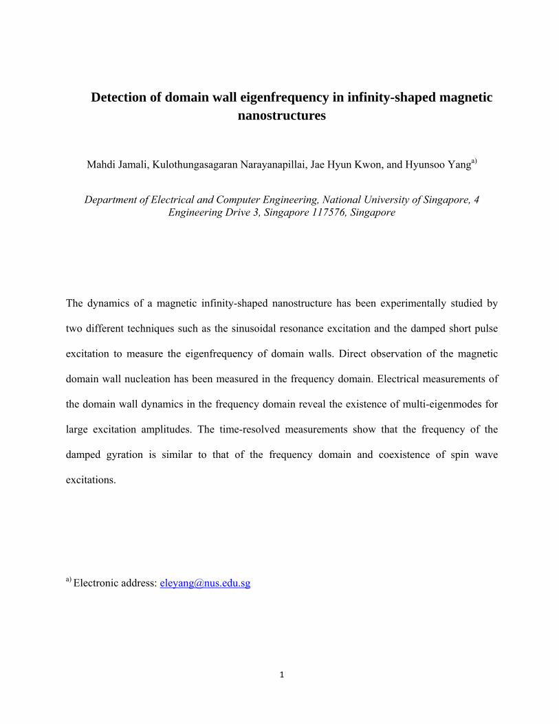
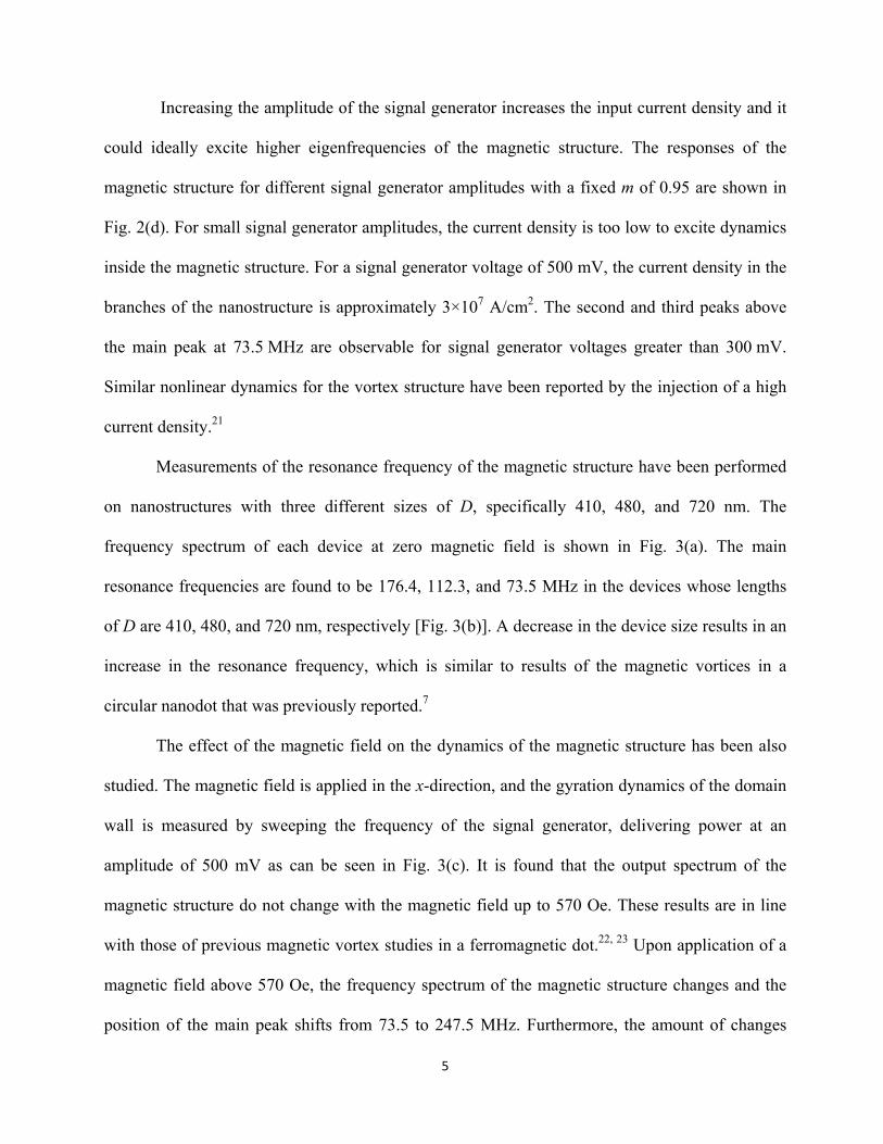
The infinity-shaped ferromagnetic nanostructure is shown in Fig. 1, which is a top-view
scanning electron microscope (SEM) image. Devices are fabricated by dc sputter deposition of Ta
(2 nm)/Ni81Fe19 (20 nm)/Ta (2 nm) on a Si/SiO2 (300 nm) substrate, followed by the patterning of
the infinity-shaped nanostructure using e-beam lithography and Ar ion milling. After ion milling,
2 nm SiO2 is rf sputter deposited without breaking the vacuum to avoid the oxidation of the
ferromagnetic nanostructure. A second e-beam lithography step is used to pattern Ta (5 nm)/Cu
(100 nm) contacts. Before contact deposition, the top surface of the ferromagnetic structure is
etched through 2 nm to clean the interface.
In order to measure magnetization dynamics, we have used the domain wall rectification
effect, and the resonance frequency of the magnetic structure has been measured using a
homodyne circuit as shown in Fig. 1. A low frequency voltage from a lock-in amplifier is mixed
with a high frequency sinusoidal signal from a microwave signal generator using an amplitude
modulator (AM) in order to excite the magnetic domain wall dynamics. The resultant signal is fed
to the device through A1A2 contacts. The voltage between B1B2 contacts is measured by the lock-
in amplifier which locks on the low frequency component. Assuming that the lock-in frequency
(ωb) is much smaller than the signal generator frequency (ωc), (i.e. ωc >> ωb), the output signal of
the amplitude modulator can be written as 0 1sin( )[1 sin( )]c c bJ t m t , where m is the
amplitude modulation constant equals to the ratio of the lock-in to signal generator amplitude, and
Jc0 is the current density. When the frequency of the signal generator is close to the resonance
frequency of the magnetic structure, the magnetic structure exhibits a resonant gyrotropic motion,
and the resistance across the magnetic domain wall in the nanostructure would contain an
oscillatory component due to the anisotropic magnetoresistance (AMR) effect.7, 9 The resultant
changes in the resistance could be written as 0 2 0 1sin( )[ sin( ){1 sin( )}]c c c bR t J t m t ,
where R0 is the change in the resistance due to the gyrotropic motion of the magnetic structure
4
that could be only excited by the high frequency component of the input signal. The amplitude of
the resultant sinusoidal voltage having a frequency ωb, which is measured by the lock-in
amplifier, is proportional to 0 0 2 10.5 cos( )cmR J , which is the phase difference between the
input signal and the change in the device resistance.9 The frequency of the signal generated by the
lock-in amplifier is set to 931.7 Hz and the signal generator frequency is swept from 10 MHz to 1
GHz in 0.5 MHz increments.
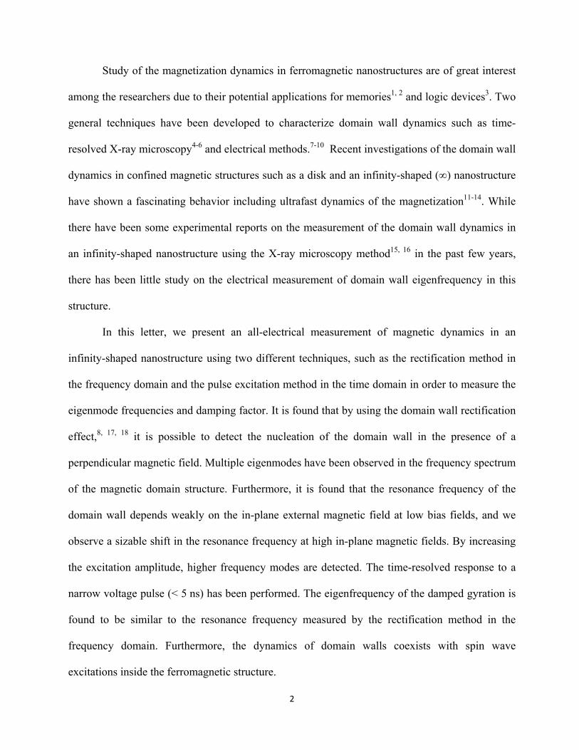
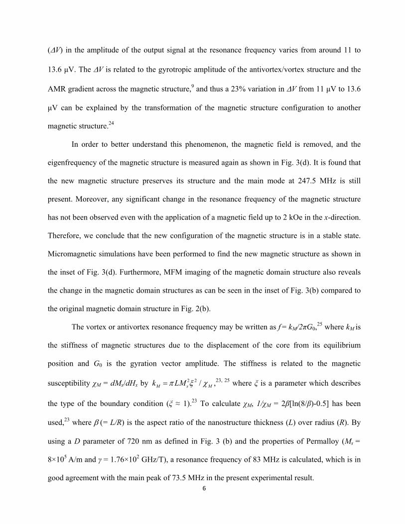
In order to nucleate magnetic domain walls in the structure, a perpendicular magnetic field
(z-direction) is applied to the nanostructure and the lock-in voltage is monitored at different
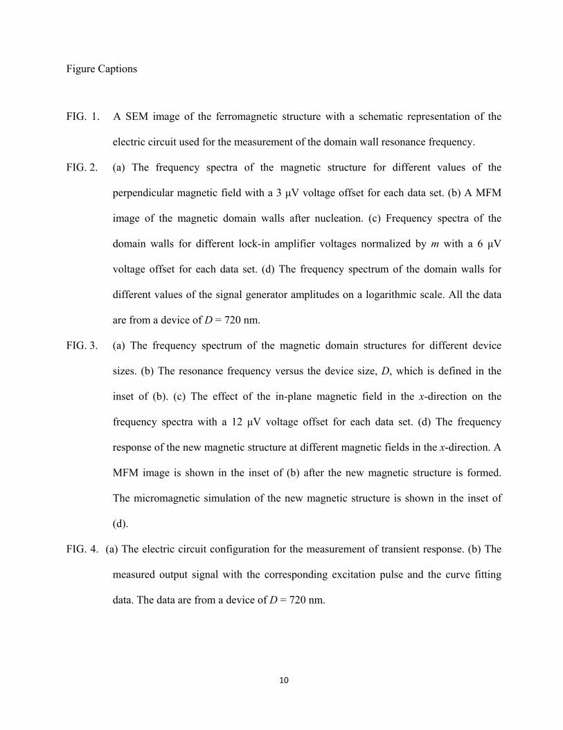
frequencies. As can be seen in Fig. 2(a), above certain values of the magnetic field (Hc = 1275
Oe), a distinct peak around 73.5 MHz appears at the output signal which was not present at lower
fields. Furthermore, by increasing the magnetic field above Hc, the peak position remains
invariant. After the external field has been turned off, we performed the measurements again. It is
found that the position of the peaks remain the same in the frequency domain. After nucleation of
domain walls, the magnetic force microscopy (MFM) data confirm the presence of magnetic
domain walls as shown in Fig. 2(b).
In order to see the effect of the amplitude of lock-in voltage on the output spectrum of the
magnetic structure, the lock-in voltage has been changed from 100 to 500 mV for a fixed signal
generator voltage of 500 mV corresponding to m = 0.2 up to m = 1. As can be seen in Fig. 2(c),
the output spectrum is almost independent of lock-in voltages, which corresponds to our
expectation that only the high frequency component of the input signal should excite the
dynamics of inside the magnetic structure. In addition, two more peaks are observed at 117.5 and
166.5 MHz, which could be either due to the different magnetic structures or due to the nonlinear
eigenmodes of the magnetic structure that have been previously reported19, 20.
5
Increasing the amplitude of the signal generator increases the input current density and it
could ideally excite higher eigenfrequencies of the magnetic structure. The responses of the
magnetic structure for different signal generator amplitudes with a fixed m of 0.95 are shown in
Fig. 2(d). For small signal generator amplitudes, the current density is too low to excite dynamics
inside the magnetic structure. For a signal generator voltage of 500 mV, the current density in the
branches of the nanostructure is approximately 3×10⁷ A/cm2. The second and third peaks above
the main peak at 73.5 MHz are observable for signal generator voltages greater than 300 mV.
Similar nonlinear dynamics for the vortex structure have been reported by the injection of a high
current density.21
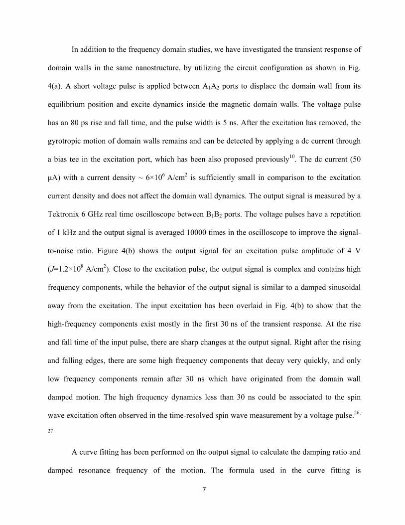
Measurements of the resonance frequency of the magnetic structure have been performed
on nanostructures with three different sizes of D, specifically 410, 480, and 720 nm. The
frequency spectrum of each device at zero magnetic field is shown in Fig. 3(a). The main
resonance frequencies are found to be 176.4, 112.3, and 73.5 MHz in the devices whose lengths
of D are 410, 480, and 720 nm, respectively [Fig. 3(b)]. A decrease in the device size results in an
increase in the resonance frequency, which is similar to results of the magnetic vortices in a
circular nanodot that was previously reported.7
The effect of the magnetic field on the dynamics of the magnetic structure has been also
studied. The magnetic field is applied in the x-direction, and the gyration dynamics of the domain
wall is measured by sweeping the frequency of the signal generator, delivering power at an
amplitude of 500 mV as can be seen in Fig. 3(c). It is found that the output spectrum of the
magnetic structure do not change with the magnetic field up to 570 Oe. These results are in line
with those of previous magnetic vortex studies in a ferromagnetic dot.22, 23 Upon application of a
magnetic field above 570 Oe, the frequency spectrum of the magnetic structure changes and the
position of the main peak shifts from 73.5 to 247.5 MHz. Furthermore, the amount of changes
6
(V) in the amplitude of the output signal at the resonance frequency varies from around 11 to
13.6 μV. The V is related to the gyrotropic amplitude of the antivortex/vortex structure and the
AMR gradient across the magnetic structure,9 and thus a 23% variation in V from 11 μV to 13.6
μV can be explained by the transformation of the magnetic structure configuration to another
magnetic structure.24
In order to better understand this phenomenon, the magnetic field is removed, and the
eigenfrequency of the magnetic structure is measured again as shown in Fig. 3(d). It is found that
the new magnetic structure preserves its structure and the main mode at 247.5 MHz is still
present. Moreover, any significant change in the resonance frequency of the magnetic structure
has not been observed even with the application of a magnetic field up to 2 kOe in the x-direction.
Therefore, we conclude that the new configuration of the magnetic structure is in a stable state.
Micromagnetic simulations have been performed to find the new magnetic structure as shown in
the inset of Fig. 3(d). Furthermore, MFM imaging of the magnetic domain structure also reveals
the change in the magnetic domain structures as can be seen in the inset of Fig. 3(b) compared to
the original magnetic domain structure in Fig. 2(b).
The vortex or antivortex resonance frequency may be written as f = kM/2πG0,25 where kM is
the stiffness of magnetic structures due to the displacement of the core from its equilibrium
position and G0 is the gyration vector amplitude. The stiffness is related to the magnetic
susceptibility χM = dMx/dHx by 2 2 /M s Mk LM ,23, 25 where ξ is a parameter which describes
the type of the boundary condition (ξ ≈ 1).23 To calculate χM, 1/χM = 2β[ln(8/β)-0.5] has been
used,23 where = L/R) is the aspect ratio of the nanostructure thickness (L) over radius (R). By
using a D parameter of 720 nm as defined in Fig. 3 (b) and the properties of Permalloy (Ms =
8×10⁵ A/m and γ = 1.76×10² GHz/T), a resonance frequency of 83 MHz is calculated, which is in
good agreement with the main peak of 73.5 MHz in the present experimental result.
7
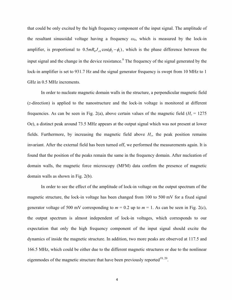
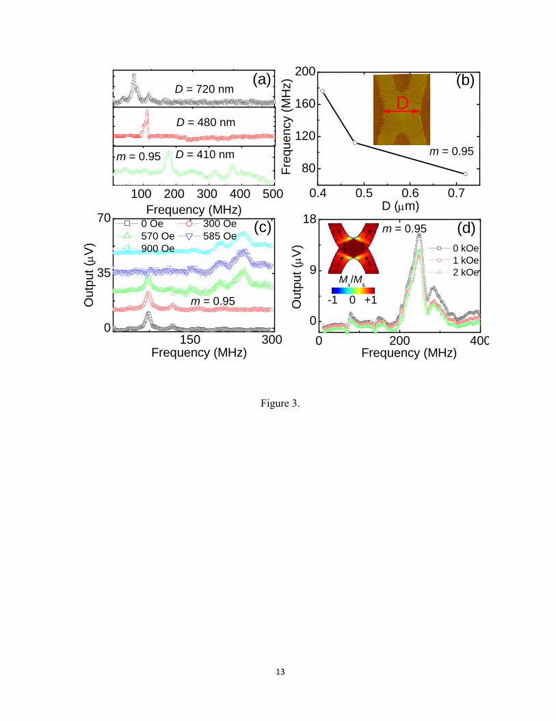
In addition to the frequency domain studies, we have investigated the transient response of
domain walls in the same nanostructure, by utilizing the circuit configuration as shown in Fig.
4(a). A short voltage pulse is applied between A1A2 ports to displace the domain wall from its
equilibrium position and excite dynamics inside the magnetic domain walls. The voltage pulse
has an 80 ps rise and fall time, and the pulse width is 5 ns. After the excitation has removed, the
gyrotropic motion of domain walls remains and can be detected by applying a dc current through
a bias tee in the excitation port, which has been also proposed previously10. The dc current (50
μA) with a current density ~ 6×10⁶ A/cm2 is sufficiently small in comparison to the excitation
current density and does not affect the domain wall dynamics. The output signal is measured by a
Tektronix 6 GHz real time oscilloscope between B1B2 ports. The voltage pulses have a repetition
of 1 kHz and the output signal is averaged 10000 times in the oscilloscope to improve the signal-
to-noise ratio. Figure 4(b) shows the output signal for an excitation pulse amplitude of 4 V
(J=1.2×10⁸ A/cm2). Close to the excitation pulse, the output signal is complex and contains high
frequency components, while the behavior of the output signal is similar to a damped sinusoidal
away from the excitation. The input excitation has been overlaid in Fig. 4(b) to show that the
high-frequency components exist mostly in the first 30 ns of the transient response. At the rise
and fall time of the input pulse, there are sharp changes at the output signal. Right after the rising
and falling edges, there are some high frequency components that decay very quickly, and only
low frequency components remain after 30 ns which have originated from the domain wall
damped motion. The high frequency dynamics less than 30 ns could be associated to the spin
wave excitation often observed in the time-resolved spin wave measurement by a voltage pulse.26,
27
A curve fitting has been performed on the output signal to calculate the damping ratio and
damped resonance frequency of the motion. The formula used in the curve fitting is
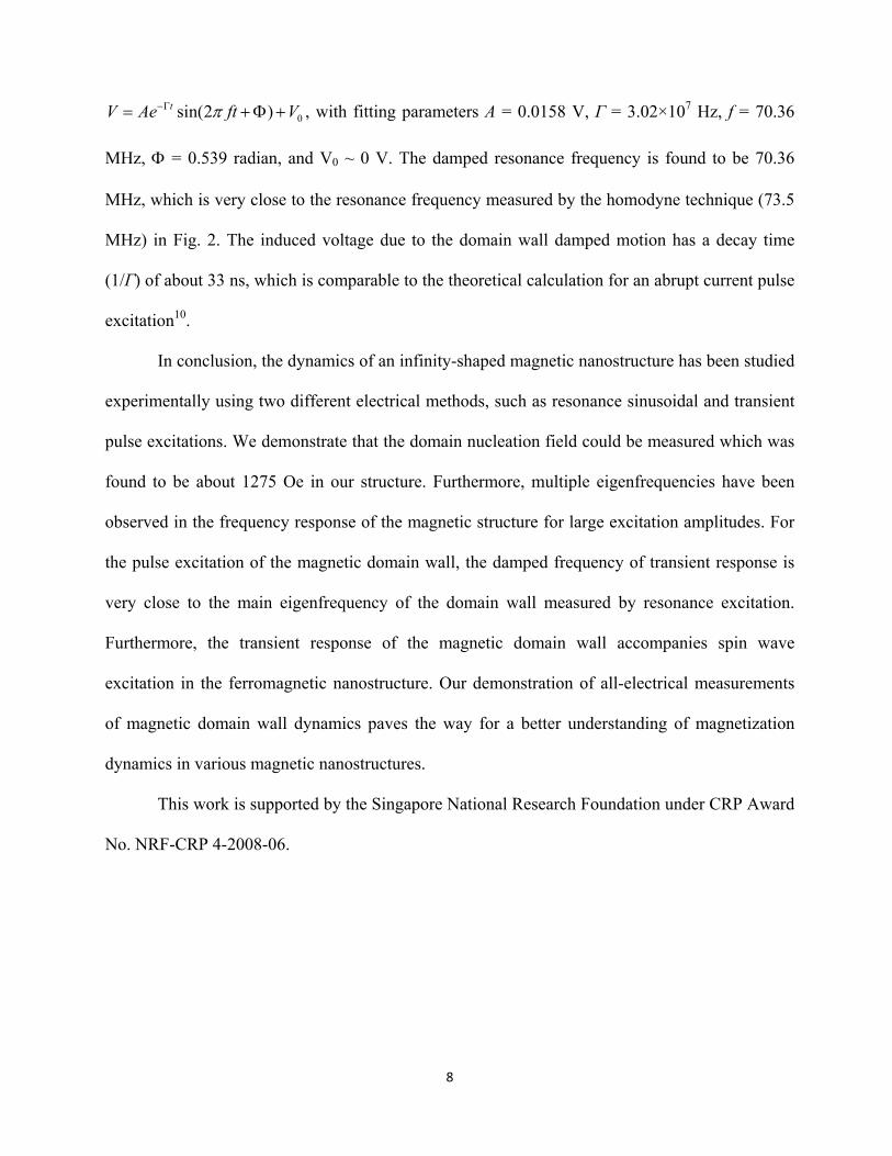
8
0sin(2 )tV Ae ft V , with fitting parameters A = 0.0158 V, Γ = 3.02×10⁷ Hz, f = 70.36
MHz, = 0.539 radian, and V0 ~ 0 V. The damped resonance frequency is found to be 70.36
MHz, which is very close to the resonance frequency measured by the homodyne technique (73.5
MHz) in Fig. 2. The induced voltage due to the domain wall damped motion has a decay time
(1/Γ) of about 33 ns, which is comparable to the theoretical calculation for an abrupt current pulse
excitation10.
In conclusion, the dynamics of an infinity-shaped magnetic nanostructure has been studied
experimentally using two different electrical methods, such as resonance sinusoidal and transient
pulse excitations. We demonstrate that the domain nucleation field could be measured which was
found to be about 1275 Oe in our structure. Furthermore, multiple eigenfrequencies have been
observed in the frequency response of the magnetic structure for large excitation amplitudes. For
the pulse excitation of the magnetic domain wall, the damped frequency of transient response is
very close to the main eigenfrequency of the domain wall measured by resonance excitation.
Furthermore, the transient response of the magnetic domain wall accompanies spin wave
excitation in the ferromagnetic nanostructure. Our demonstration of all-electrical measurements
of magnetic domain wall dynamics paves the way for a better understanding of magnetization
dynamics in various magnetic nanostructures.
This work is supported by the Singapore National Research Foundation under CRP Award
No. NRF-CRP 4-2008-06.

9
References:
1 M. Hayashi, L. Thomas, R. Moriya, C. Rettner, and S. S. P. Parkin, Science 320, 209 (2008). 2 S. Bohlens, B. Kruger, A. Drews, M. Bolte, G. Meier, and D. Pfannkuche, Appl. Phys. Lett. 93,
142508 (2008). 3 D. A. Allwood, G. Xiong, C. C. Faulkner, D. Atkinson, D. Petit, and R. P. Cowburn, Science 309,
1688 (2005). 4 M. Bolte, G. Meier, B. Kruger, A. Drews, R. Eiselt, L. Bocklage, S. Bohlens, T. Tyliszczak, A.
Vansteenkiste, B. Van Waeyenberge, K. W. Chou, A. Puzic, and H. Stoll, Phys. Rev. Lett. 100, 176601 (2008).
5 J. Raabe, C. Quitmann, C. H. Back, F. Nolting, S. Johnson, and C. Buehler, Phys. Rev. Lett. 94, 217204 (2005).
6 A. Bisig, J. Rhensius, M. Kammerer, M. Curcic, H. Stoll, G. Schutz, B. Van Waeyenberge, K. W. Chou, T. Tyliszczak, L. J. Heyderman, S. Krzyk, A. von Bieren, and M. Klaui, Appl. Phys. Lett. 96, 152506 (2010).
7 S. Kasai, Y. Nakatani, K. Kobayashi, H. Kohno, and T. Ono, Phys. Rev. Lett. 97, 107204 (2006). 8 R. Moriya, L. Thomas, M. Hayashi, Y. B. Bazaliy, C. Rettner, and S. S. P. Parkin, Nat. Phys. 4, 368
(2008). 9 J. S. Kim, O. Boulle, S. Verstoep, L. Heyne, J. Rhensius, M. Kläui, L. J. Heyderman, F. Kronast, R.
Mattheis, C. Ulysse, and G. Faini, Phys. Rev. B 82, 104427 (2010). 10 Y. Liu, O. A. Tretiakov, and A. Abanov, Phys. Rev. B 84, 052403 (2011). 11 R. Hertel, S. Gliga, M. Fahnle, and C. M. Schneider, Phys. Rev. Lett. 98, 117201 (2007). 12 K.‐S. Lee, K. Y. Guslienko, J.‐Y. Lee, and S.‐K. Kim, Phy. Rev. B 76, 174410 (2007). 13 K. Yamada, S. Kasai, Y. Nakatani, K. Kobayashi, H. Kohno, A. Thiaville, and T. Ono, Nat. Mater. 6,
270 (2007). 14 S. Gliga, M. Yan, R. Hertel, and C. M. Schneider, Phys. Rev. B 77, 060404 (2008). 15 T. Kamionka, M. Martens, K. W. Chou, M. Curcic, A. Drews, G. Schutz, T. Tyliszczak, H. Stoll, B. Van
Waeyenberge, and G. Meier, Phys. Rev. Lett. 105, 137204 (2010). 16 K. Kuepper, M. Buess, J. Raabe, C. Quitmann, and J. Fassbender, Phys. Rev. Lett. 99, 167202
(2007). 17 A. Yamaguchi, H. Miyajima, T. Ono, Y. Suzuki, and S. Yuasa, Appl. Phys. Lett. 91, 132509 (2007). 18 A. Thiaville and Y. Nakatani, J. Appl. Phys. 104, 093701 (2008). 19 K. Y. Guslienko, R. Rafael Hernández, and O. Chubykalo‐Fesenko, Phys. Rev. B 82, 014402 (2010). 20 X. M. Cheng, K. S. Buchanan, R. Divan, K. Y. Guslienko, and D. J. Keavney, Phys. Rev. B 79, 172411
(2009). 21 D. Bedau, M. Kläui, M. T. Hua, S. Krzyk, U. Rüdiger, G. Faini, and L. Vila, Phys. Rev. Lett. 101,
256602 (2008). 22 V. Novosad, F. Y. Fradin, P. E. Roy, K. S. Buchanan, K. Y. Guslienko, and S. D. Bader, Phys. Rev. B
72, 024455 (2005). 23 K. Y. Guslienko, B. A. Ivanov, V. Novosad, Y. Otani, H. Shima, and K. Fukamichi, J. Appl. Phys. 91,
8037 (2002). 24 L. Bocklage, B. Krüger, R. Eiselt, M. Bolte, P. Fischer, and G. Meier, Phys. Rev. B 78, 180405 (2008). 25 R. L. Compton, T. Y. Chen, and P. A. Crowell, Phys. Rev. B 81, 144412 (2010). 26 M. Covington, T. M. Crawford, and G. J. Parker, Phys. Rev. Lett. 89, 237202 (2002). 27 J. H. Kwon, S. S. Mukherjee, M. Jamali, M. Hayashi, and H. Yang, Appl. Phys. Lett. 99, 132505
(2011).
10
Figure Captions
FIG. 1. A SEM image of the ferromagnetic structure with a schematic representation of the
electric circuit used for the measurement of the domain wall resonance frequency.
FIG. 2. (a) The frequency spectra of the magnetic structure for different values of the
perpendicular magnetic field with a 3 μV voltage offset for each data set. (b) A MFM
image of the magnetic domain walls after nucleation. (c) Frequency spectra of the
domain walls for different lock-in amplifier voltages normalized by m with a 6 μV
voltage offset for each data set. (d) The frequency spectrum of the domain walls for
different values of the signal generator amplitudes on a logarithmic scale. All the data
are from a device of D = 720 nm.
FIG. 3. (a) The frequency spectrum of the magnetic domain structures for different device
sizes. (b) The resonance frequency versus the device size, D, which is defined in the
inset of (b). (c) The effect of the in-plane magnetic field in the x-direction on the
frequency spectra with a 12 μV voltage offset for each data set. (d) The frequency
response of the new magnetic structure at different magnetic fields in the x-direction. A
MFM image is shown in the inset of (b) after the new magnetic structure is formed.
The micromagnetic simulation of the new magnetic structure is shown in the inset of
(d).
FIG. 4. (a) The electric circuit configuration for the measurement of transient response. (b) The
measured output signal with the corresponding excitation pulse and the curve fitting
data. The data are from a device of D = 720 nm.

11
Figure 1.
12
100 2000
15
30
100 200100 2000
20
40(d)(c)
0 Oe 600 Oe900 Oe 1275 Oe1500 Oe 1800 Oe
Out
put
(V
)
Frequency (MHz)
Hzm = 0.95
(b)
100 mV 200 mV 300 mV 400 mV 500 mV 900 mV
Am
plitu
de (
a.u.
)
Frequency (MHz)
100 mV 200 mV 300 mV 400 mV 500 mV
Out
put
(V
)
Frequency (MHz)
(a)
m = 0.95
Figure 2.
13
100 200 300 400 500 0.4 0.5 0.6 0.7
80
120
160
200
150 3000
35
70
0 200 400
0
9
18
D = 410 nm
D = 480 nm
D = 720 nm
(a)
Frequency (MHz)
Fre
quen
cy (
MH
z)
D (m)
D
m = 0.95
m = 0.95
m = 0.95
Out
put
(V
)
0 Oe 300 Oe 570 Oe 585 Oe 900 Oe
m = 0.95
(b)
(d)(c)
Frequency (MHz)
0 +1
Out
put
(V
)
Frequency (MHz)
0 kOe 1 kOe 2 kOe
Mx/M
s
-1
Figure 3.

14
A1 A
2
B1 B
2
0 40 80-100
-50
0
50
100
Measurement Curve fitting
Time (ns)O
utpu
t (m
V)
0
1
2
3
4(b)
Input pulse
Exc
itatio
n (V
)
Pulse width = 5 nsPulse amplitude = 4 VIdc
= 50 A
(a)
Figure 4